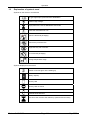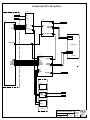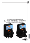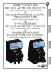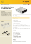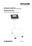
1
Semiautomatic defibrillator (PAD) Service Manual Version 01.00 Part No. 0-48-0029 FRED EASY Revision history of the service manual Version 01.00: Part no. 0-48-0029 May 2003 Page I May 2003 FRED EASY WARNING This manual shall be considered to form an integral part of the device described. This technical manual is intended for qualified personnel and describes the operating, maintenance and troubleshooting procedures for FRED EASY. Compliance with its content is a prerequisite for proper device performance and for the safety of the patient and operator. The manufacturer shall only be liable for the safety, reliability and performance of the device if: - assembly, extensions, adjustments, modifications or repairs are performed by the manufacturer or by persons authorised by the manufacturer. - the electrical installation of the facility of use complies with the requirements applicable in the country. - the device is used in accordance with its instructions for use. - the spare parts used are original parts from SCHILLER. This manual describes the device at the time of printing. The supply of this manual does not in any event constitute permission or approval to modify or repair a device. The manufacturer agrees to supply all the spare parts for a period of ten years. All rights reserved for the devices, circuits, processes and names appearing in this manual. The FRED EASY device shall be used as described in the User’s Manual. The device may not be used for any purpose that has not been specifically described in the manual, as such use could be hazardous. Part no. 0-48-0029 Page II May 2003 FRED EASY SAFETY INFORMATION ! The product is marked as follows: CE- 0459 in accordance with the requirements of Council Directive 93/42/EEC relating to medical equipment, based on the essential requirements of annex I of the directive. ! It fully meets the electromagnetic compatibility requirements of standard IEC 60601-1-2/EN 60601-2 “Electromagnetic compatibility of medical electrical devices”. ! The device has undergone interference suppression in accordance with the requirements of standard EN 50011, class B. ! ! In order to optimise patient safety, electromagnetic compatibility, accurate measurement indication and proper device performance, users are advised to use only original spare parts supplied by SCHILLER. Any use of accessories other than original accessories shall be at the exclusive risk of the user. The manufacturer shall not be liable for any damage due to the use of incompatible accessories or consumable supplies. The manufacturer shall only be liable for the safety, reliability and performance of the device if: - assembly, configuration, modifications, extensions or repairs are made by personnel from SCHILLER MEDICAL or personnel duly authorised by SCHILLER MEDICAL. - the device is used in accordance with its instructions for use. ! ! Any use of the device other than as described in the instructions for use shall be made at the exclusive risk of the user. This manual covers the device version and the safety standards applicable at the time of printing. All rights reserved for the circuits, processes, names, software and devices appearing in this manual. ! The quality assurance system in use in the facilities of SCHILLER meets international standards EN ISO 9001 and EN 46001. ! Unless otherwise agreed in writing by SCHILLER, no part of the manufacturer’s literature may be duplicated or reproduced. Part no. 0-48-0029 Page III May 2003 FRED EASY Safety symbols used on the device Danger! High voltage Conventions used in the manual Danger: indicates an imminent hazard which, if not avoided, will result in death or serious injury to the user (and/or others). Caution: Warning indicating conditions or actions that could lead to device or software malfunctioning. Note: Useful information for more effective and operation. ! " # practical device Additional information or explanation relating to the paragraphs preceding the note. Manufacturer: SCHILLER MEDICAL SA 4, rue Louis Pasteur ZAE sud F- 67 162 Wissembourg Tel. Fax : **33 / (0) 3.88.63.36.00 : **33 / (0) 3.88.94.12.82 Part no. 0-48-0029 Page IV May 2003 FRED EASY PRECAUTIONS WHILE TESTING THE DEVICE While testing the FRED EASY defibrillator, the patient may only be simulated with fixed high-voltage and high-power resistors that are well insulated from the ground or earth. Poorly insulated devices or devices with loose contacts or devices containing components such as spark arresters or electronic flash lamps may never be used as they could irremediably destroy the device. Part no. 0-48-0029 Page V May 2003 FRED EASY CONTENTS 1. Operation_________________________________________________________ 1-1 1.1 Display and controls _____________________________________________________ 1-1 1.2 Explanation of symbols used ______________________________________________ 1-2 1.3 Device operation ________________________________________________________ 1-3 1.4 Defibrillation procedure ___________________________________________________ 1-3 1.5 Recording (optional) _____________________________________________________ 1-6 1.6 Technical specifications __________________________________________________ 1-7 2. Testing and maintenance ____________________________________________ 2-1 2.1 Functional testing _______________________________________________________ 2-1 2.2 Systematic verification before use __________________________________________ 2-3 2.3 Cleaning and disinfecting _________________________________________________ 2-3 3. Troubleshooting____________________________________________________ 3-1 4. Replacement of parts _______________________________________________ 4-1 4.1 Device disassembly procedure _____________________________________________ 4-2 4.2 Working on the CPU circuit________________________________________________ 4-3 4.3 Working on the LCD display _______________________________________________ 4-3 4.4 Working on the DEFI circuit _______________________________________________ 4-3 4.5 Replacing the high-voltage capacitor ________________________________________ 4-3 4.6 Reassembling the device _________________________________________________ 4-5 4.7 Replacement of parts ____________________________________________________ 4-5 5. Technical description of boards________________________________________ 5-1 5.1 FRED easy ____________________________________________________________ 5-1 5.2 CPU (part no. WSM0005A)________________________________________________ 5-3 5.3 Defibrillator, part no. WSM0008A __________________________________________ 5-28 5.3.1 5.3.2 5.3.3 5.3.4 5.3.5 5.3.6 5.3.7 5.3.8 6. Driving the high-voltage capacitor charge_______________________________________ Chronograms ____________________________________________________________ Description of signals ______________________________________________________ ECG preamplifier _________________________________________________________ Defibrillator control circuit ___________________________________________________ High-voltage circuit ________________________________________________________ IGBT control circuit ________________________________________________________ Fault detection circuit ______________________________________________________ 5-33 5-40 5-43 5-43 5-44 5-48 5-50 5-52 Device modifications ________________________________________________ 6-1 6.1 Definition ______________________________________________________________ 6-1 6.2 CPU circuit ____________________________________________________________ 6-1 6.3 DEFI circuit ____________________________________________________________ 6-1 7. Diagrams and layout drawings ________________________________________ 7-1 7.1 CPU circuit WSM0005A __________________________________________________ 7-1 7.2 Defi circuit WSM0008A ___________________________________________________ 7-4 Part no. 0-48-0029 Page VI May 2003 Operation 1. Operation This section briefly outlines the operating of the device. For more detailed information, please refer to the User’s Manual. 1.1 a b c d e f g Display and controls The green indicator lamp flashes when the device is ready to operate. The yellow indicator lamp flashes as long as the electrodes are not in place. Connection of adhesive electrodes key to switch the device on and off and start analysing Green Key for triggering the defibrillation shock Memory card (optional) Battery Part no. 0-48-0029 Page 1-1 May 2003 Operation 1.2 Explanation of symbols used Symbols on the device or accessories BF type signal input, protected from defibrillation Caution! High voltage! Expiry date for the use of defibrillation electrodes Follow the instructions for use Open the electrode packaging Remove the protective film Single use only. Do not reuse. Do not fold the packaging Storage temperature range Symbols displayed on the screen Number of shocks given since starting up Battery capacity Memory card Memory card not found Adult electrode detected Child electrode detected Time since the machine was started up (minutes and seconds) Part no. 0-48-0029 Page 1-2 May 2003 Operation 1.3 Device operation FRED easy® is a battery-operated semiautomatic defibrillator that provides biphasic defibrillation pulses. Defibrillation takes place by means of single-use adhesive electrodes through which the ECG signals required for the analysis are also collected. Adhesive electrodes are available for children and adults. The device recognises the type of electrode applied and selects the defibrillation energy values accordingly. The user is provided with written and audio instructions (display and loudspeaker) relating to the use of the device. The power is supplied by plug-in disposable lithium batteries. Their capacity is sufficient for - 200 shocks at the maximum power rating or - use of the monitor for seven hours (cyclical, 30 minutes on, 30 minutes off) or - 5 years standing by. As soon as a battery is put in place in the FRED easy® device, it runs a self test to check the status of the device and battery. If the device does not find any fault, the green indicator begins to flash to show that it is ready to operate and the display disappears. Likewise, the device runs a self test each time it is switched on. If, during the test, the device finds an error: - it issues an audio alarm, - the green indicator does not flash The alarm signal rings till the battery is completely discharged. Key error message is displayed. is used to repeat the self test and the Also, the device runs a self test after every seven days. The test is announced by a beep. If, during the test, the device finds an error: - it issues an audio alarm, - the green indicator does not flash the corresponding error message is displayed. If you press key In that case, you must replace the battery and repeat the test. Depending on the test result, the error message will disappear or another message will be displayed. 1.4 Defibrillation procedure All the stages are explained orally to the user at the same time as they are displayed on the screen. Once key is pressed, the introductory text tells the user what is to be done if the patient has the following symptoms: - the patient has ceased to breathe, - there is no sign of circulation. The introductory text is repeated till the FRED easy® device recognises the application of the adhesive electrodes. Depending on the configuration, the introductory text may be deleted and the device directly requests the application of the adhesive electrodes. After that, the FRED easy® device asks the user to start an ECG analysis and to no longer touch the patient. The analysis lasts approximately 10 s. Depending on the configuration, the device starts the ECG analysis automatically. Note - With the signals from the AHA (American Heart Association) database, the detection accuracy of FRED easy® was found to be 98.43 % (sensitivity), with a specificity rate of 99.80 %. - The device may be configured so that it automatically starts the ECG analysis. If the analysis program recognises a heart rate that calls for defibrillation, it automatically charges the energy required for defibrillation and asks the user to deliver the shock after the energy is charged. The following are considered to warrant defibrillation: - ventricular fibrillation or - ventricular tachycardia with a heart rate of over 180 bpm. Part no. 0-48-0029 Page 1-3 May 2003 Operation If the device finds a heart rate that calls for defibrillation, defibrillation is only authorised if the patient is found to have no pulse or if there are no signs of circulation. If the defibrillation shock has no effect, the device automatically charges the energy required for a second or even a third shock. Note The energy values are set by default as follows (the technical assistance of SCHILLER can configure other default values if needed). Shock Adult Child 1 90 J 15 J 2 130 J 30 J 3 150 J 50 J If the third shock is also ineffective, the FRED easy® device asks to user to alternately administer artificial respiration and heart massage. After a minute, an ECG analysis will be requested once again. Depending on the configuration, the new analysis may be automatic. After a successful defibrillation shock, the FRED easy® device asks the user to check the patient’s breathing and blood circulation. If there is no sign of circulation, the device asks the user to alternately administer artificial respiration and heart massage. If there is any sign of circulation, the patient must be laid on his or her side. If the analysis program does not recognise a heart rate calling for defibrillation, - FRED easy® informs the user that defibrillation is not necessary and - asks the user to look for breathing and signs of circulation. If there is no sign of circulation, the FRED easy® device asks the user to alternately administer artificial respiration and heart massage. If there are any signs of circulation, the user is asked to lay the patient on his or her side. After a minute, the FRED easy® device repeats the request for an ECG analysis. Depending on the configuration, the new analysis may be automatic. The following values can be configured by the technical assistance department of SCHILLER: - upon starting up: introductory text or immediate request to apply the adhesive electrodes, - voice volume, - energy levels of shocks 1, 2 and 3, with adult and child separate - starting of the ECG analysis via the keypad or automatically. Part no. 0-48-0029 Page 1-4 May 2003 Operation Procedure chart Part no. 0-48-0029 Page 1-5 May 2003 Operation 1.5 Recording (optional) For information, the memory board can save the following: - half an hour of ECG - half an hour of speech, - 500 events relating to the procedure (see overview opposite). Plugging in a memory card activates the memory function and the display includes the icon . The memory card is analysed by means of a PC, with the SAED Reader software. Icon flashes when the memory card is full. Important! The device must be switched off when you insert the card. Otherwise, the device will not recognise the card and will display the following symbol: If no symbol is displayed even after the card has been put in place, you must make sure that the card is indeed a card designed for such devices by SCHILLER. Part no. 0-48-0029 Page 1-6 May 2003 Operation 1.6 ! ! ! ! ! ! ! ! ! ! ! Technical specifications Form of the defibrillation pulse - Modulated defibrillation pulse with two pulse phases and physiologically optimised phase duration of 4 ms. - Constant value of the average current delivered and the energy discharged depending on patient impedance, using pulse modulations in the pause position in the two phases. - Modulation of the second phase (negative phase) so that the residual charges of the first phases are degraded in the heart. Standard energy settings: - Adult (discharge in 50 .): 90 -130 -150 J - Child (automatic switch when child electrodes are connected): 15 -30 -50 J - The energy levels can be configured by the technical assistance department of Schiller if the standard values need to be changed: 1 - 2 - 4 - 6 - 8 - 15 - 30 - 50 - 70 - 90 - 110 - 130 - 150 J (Adult) 1 - 2 - 4 - 6 - 8 - 15 - 30 - 50 - 70 (Child) - Tolerance at 50 ȍ: ± 3 J or ± 15 % (whichever is greater). Automatic charge control after a shock is recommended following an analysis Patient resistance 30 - 175 . Charge duration, from the time a shock is recommended up to the time when the device is ready: < 10 s Cycle time between two shocks: < 20 s Indication that the devices is ready to deliver a shock: key goes on. The shock is delivered with key Internal safety discharge if: - the heart rate does not call for defibrillation - after 20 seconds of the device indicating its readiness for a shock, no shock is delivered - there is an electrode fault - the battery voltage is insufficient - the device is faulty - the device is switched off The shock is delivered with single-use adhesive electrodes applied in the anterior / anterior-lateral positions BF type defibrillation electrode connector. Part no. 0-48-0029 Page 1-7 May 2003 Operation ! ! ! ! ! ! ! ! Defibrillation electrodes: - Adult electrodes: Active area 78 cm² - Child electrodes: Active area 28 cm² - Electrode cable length: 2 m VT / VF recognition: - Shock recommendation: for VF and VT (VT > 180 bpm) - Sensitivity: 98.43 % Specificity: 99.8 %. These values have been found with the AHA database, which contains cases of VF and VT with and without artefacts. - Conditions required for ECG analysis: Minimum amplitude for the signals used > 0.15 mV , signals of < 0.15 mV are considered to show asystole. - Definition: Sensitivity: Correct detection of heart rates for which defibrillation shocks are recommended Specificity: Correct detection of heart rates for which defibrillation shocks are not recommended Display: - LCD, 100 x 37 mm, high definition, with EL backlighting, display of text and icons. Recording of the use of the device (optional) - ECG recording (half an hour) - Voice recording (half an hour) - Event recording (500 events) Lithium battery capacity - 200 shocks at the maximum power rating or - Use of the monitor for seven hours (cyclical, 30 minutes on, 30 minutes off) - Five years standing by. Environment conditions: - Transport / storage: Temperature - 30 to + 50 °C Relative humidity of air 0 to 95 %, non condensing Atmospheric pressure 500 - 1060 hPa - Use: Temperature - 30 to + 50 °C Relative humidity of air 0 to 95 %, non condensing Atmospheric pressure 700 - 1060 hPa Electromagnetic compatibility: - The FRED easy® device only uses radio frequency range energy for its internal functions. It is treated against interference in accordance with standard CISPR 11 class B - The FRED easy® device can be subjected to the following interference without any adverse effect on its functioning: ! electrostatic discharges of up to 8 kV. ! energy in the radio frequency range up to 20 V/m (80 - 2500 MHz, 5 Hz modulated). ! magnetic fields of 100 A/m, 50 Hz Dimensions and weight: - Width : 220 mm - Depth : 230 mm - Height : 70 mm - Approximate weight : 1.5 kg (with battery) Part no. 0-48-0029 Page 1-8 May 2003 Testing and maintenance 2. Testing and maintenance This section describes the testing and maintenance procedures recommended for FRED easy. 2.1 Functional testing The device runs an automatic functional test. In order to ensure proper performance, tests are performed when the device starts in the nominal mode (SAD mode), once a week and each time a battery is inserted. The Test mode defines specific device behaviour and is used to test its vital functions. The functioning of the Test mode is not redundant with the self test phase. The aim of the self test is to check the vital functions of the device when it is switched on. The aim of the Test mode is to regularly check the vital parts of the device in order to ensure that it will continue to perform even when it is used occasionally. The device is also in the Test mode when a battery is inserted. In that case, specific tests are defined. Specific case of self tests: Self tests are performed automatically when the device is switched on and require no action by the operator. No message describing the test under way is displayed when the device runs its self tests. A message is displayed to merely show that the device is about to start – “STARTING …”. The software version of the device is also displayed during the self test. The self test consists in checking the following functions: ! ADC converter test – it is used to validate the functioning of the analogue to digital converter used to acquire battery parameters (voltage and temperature) and patient parameters (ECG 250Hz, MVTS, impedance variation, patient impedance) ! Defibrillator test, level 1 – used to validate the status of the defibrillator hardware and particularly to ensure that communication with the defibrillator is operational and that the defibrillation hardware module has not found any error. ! EEPROM configuration test – it is used to make sure that access to the EEPROM containing device configuration information is valid and that the information is consistent ! RTC test – used to validate the operating of the real time clock of the device ! Battery test – used to validate the battery level (the test shows an error if the remaining battery charge is 0%) ! LCD test – used to validate the display ! OKI test – used to validate the speech prompt system ! Encoder test – used to validate the operating of the sound environment acquisition system If any of the tested peripherals shows an error, the device cannot be used. In that case, the device status display (flashing LED) is changed to indicate that the device may not be used – the LED goes off – and a message indicates the test that has failed. When the LED goes off, a buzzer is triggered to indicate a device fault. If the tests succeed, the device executes the SAD operating mode. Part no. 0-48-0029 Page 2-1 May 2003 Testing and maintenance Specific case of periodic tests: Because the device is used in emergency situations, it must be ready to operate when it is needed. As a result, self tests are insufficient. That is why periodic testing is performed to maximise the chances of detecting any error in the device, including when it is not used. Periodic testing includes the following operations: ! Self tests ! Level 2 hardware test of the defibrillator module – test of a battery test command by the defibrillator module. This test is used to check that the power source of the device (lithium cell or battery) makes it possible to charge the device. ! ECG acquisition circuit test – checking the functioning of the ECG signal acquisition chain, which acts as the basis for analysing the patient’s heart signal. This test is used to make sure that the data on which the diagnostic is based are consistent. The tests are performed automatically from time to time. Every week at 12.00 hours, the tests are performed if the device is off. The clock wakes the device for the requisite operations. The alarm date is configurable by means of the configuration PC. Periodic tests are logged in order to be able to determine the nature of any failure and the time when the failure occurred. The last thirty results of periodic testing are logged in the memory. The memory can be read simply by means of a PC, in the configuration and transfer mode. That makes it possible to identify the origin of the problem found. The logged data include the following: ! test date ! test time ! test result ! origin of the problem found, if the result shows an error The detection of a problem during a periodic test makes the device impossible to use. The Status display is changed in order to indicate that a problem has been found. Nothing is displayed during the periodic tests in order to maximise the use of machine power. That is why the Status display is the only means of indication. When the device is switched on again, an error message indicates the problem found during periodic testing. Each time the device is switched on, the error message is displayed. The error disappears when the problem is corrected and when new tests succeed after battery insertion. If the tests are successful, the device is switched off. Specific case of battery insertion tests: Given that periodic tests cannot be performed when the device no longer has a battery, the device must be tested as soon as a new battery is inserted, in order to indicate any fault as soon as possible. Tests are triggered as soon as a battery is inserted in the device. In that case, the test and the operations performed are: ! Self tests if no error is found during previous periodic tests ! Self tests, level-2 hardware test of the defibrillator module and ECG acquisition circuit tests, if an error has been found during the previous periodic tests. If any of the tested peripherals shows an error, the device cannot be used. In that case, the device status display (flashing LED) is changed to indicate that the device may not be used – the LED goes off – and a message indicates the test that has failed. Part no. 0-48-0029 Page 2-2 May 2003 Testing and maintenance If the battery insertion test is successful and if the last logged periodic test has failed, the battery insertion test is logged. The logged data include: ! test date ! test time ! test result - OK ! reset information, to indicate that a problem had been found during periodic tests and has been corrected. If the tests are completed successfully, the device goes off automatically at the end of the operation. Otherwise, the device stays on to indicate the failed test. 2.2 Systematic verification before use Before each use of the device, the device, cables, connectors and electrodes must undergo a visual inspection. If you find any faults or malfunctioning that could impact the safety of the patient or the user, do not use the device before it is repaired. Systematic verification before each use ! Verification of the device housing ! No mechanical damage ! No penetration of liquid in the device ! Check the condition of the control buttons and the connectors. 2.3 Cleaning and disinfecting " Caution: Switch the device off before cleaning it. Remove the cell before you start cleaning the device in order to eliminate the risk of the device starting up accidentally. Also disconnect the defibrillation electrodes of the device before cleaning. No liquid shall be allowed to enter into the device. However, if that does happen, the device may not be used before it is verified by the after-sales service department. The device or electrodes may never be cleaned with substances such as ether, acetone, esters, aromatic chemicals etc. Never use phenol-based cleaners or cleaners containing peroxide derivatives to disinfect the surfaces of the housing of the device. ! Dispose of all single-use electrodes immediately after use in order to eliminate the risk of accidental reuse (disposal with hospital waste). ! Before cleaning the electrode cables of sensors, disconnect them from the device. For cleaning and disinfecting, wipe the cables with a gauze cloth moistened with cleaner or disinfectant. Never immerse the connectors in liquid. The cleaning solution used may be any cleaning or disinfecting solution that is commonly used in hospitals. ! Proceed likewise with the device housing, with a cloth moistened with cleaner or disinfectant. No liquid may be allowed to penetrate into the device during the operation. Part no. 0-48-0029 Page 2-3 May 2003 Troubleshooting 3. Troubleshooting This section addresses the troubleshooting procedures for FRED easy®. If you have trouble locating or correcting the problem, contact the after-sales service department of Schiller. Precautions during troubleshooting While testing the FRED EASY defibrillator, the patient may only be simulated with fixed high-voltage and high-power resistors that are well insulated from the ground or earth. Poorly insulated devices or devices with loose contacts or devices containing components such as spark arresters or electronic flash lamps may never be used as they could irremediably destroy the device. The user’s manual contains a troubleshooting table intended for the user. ERROR FINDING POSSIBLE CAUSES CORRECTIVE ACTION The device is not switched on when the battery is inserted. 1. Cell fault 2. Incorrect insertion 3. Problem with contacts 4. Problem with fuses 1. Replace the cell 2. Repeat the insertion 3. Check contacts 4. Check fuses When the cell is inserted, the self test succeeds but the OK indicator does not flash. 1. Fuse F1 on CPU board faulty 1. Replace fuse No display of message: FRED IS TESTING 1. Check the button cell on the CPU (out of order or down) 2. Check if F1 is faulty on DEFI board 3. CPU board faulty 4. DEFI board faulty 1. Replace the button cell When the cell is inserted, no self test but the OK indicator flashes. 1. CPU board faulty 1. Replace CPU The self test succeeds, but the OK indicator does not flash. The screen stays on for 5 s 1. CPU board faulty 1. Replace CPU The On/Off key does not respond. 1. CPU board faulty 1. Replace CPU 1. DEFI board 1. Replace DEFI board Message: DEFIBRILLATOR CPU ERROR Part no. 0-48-0029 No display and/or no voice messages Page 3-1 2. Replace fuse 3. Replace CPU 4. Replace DEFI board May 2003 Troubleshooting Message: DEFIBRILLATOR INTEGRITY ERROR PROGRAM 1. DEFI board 1. Replace DEFI board Message: DEFIBRILLATOR DETECTOR ERROR 1. DEFI board 1. Replace DEFI board Message: DEFIBRILLATOR ERROR VOLTAGE REFERENCE 1. DEFI board 1. Replace DEFI board Message: DEFIBRILLATOR CONVERTER ERROR ADC 1. DEFI board 1. Replace DEFI board Message: DEFIBRILLATOR CHARGE TRANSISTOR ERROR 1. DEFI board 1. Replace DEFI board Message: DEFIBRILLATOR SAFETY DISCHARGE ERROR 1. DEFI board 1. Replace DEFI board Message: DEFIBRILLATOR EPROM ERROR 1. CPU board 1. Replace CPU board Message: DEFIBRILLATOR SHOCK BUTTON ERROR 1. CPU board 2. DEFI board 1. Replace CPU board 2. Replace DEFI board Message: DEFIBRILLATOR COMMUNICATION ERROR 1. CPU board 2. DEFI board 1. Replace CPU board 2. Replace DEFI board Message: SYSTEM ERROR 1. CPU board 1. Replace CPU board 1. CPU board 1. Replace CPU board Fault detected during the self test Part no. 0-48-0029 Monitor on, but the OK LED does not flash Page 3-2 May 2003 Troubleshooting Cell symbol flashing, but no remaining % 1. Cell contact fault 1.1 Check cell contact 1.2 Replace cell Electrodes not connected and LED under electrode connection off 1. DEFI board faulty 2. CPU board faulty 1. Replace DEFI board 2. Replace CPU board Electrodes connected to simulator with 50-ohm impedance, but the LED does not go off 1. DEFI board faulty 2. CPU board faulty 1. Replace DEFI board 2. Replace CPU board No cell voice message 1. Speaker fault 2. CPU board fault 1. Replace speaker 2. Replace CPU board 1. Buzzer fault 2. CPU board fault 1. Replace buzzer 2. Replace CPU board Green Analysis key or orange Shock key not on 1. CPU board fault 1. Replace CPU board Abnormal internal discharge 1. DEFI board faulty 1. Replace DEFI board No shock delivered 1. DEFI board faulty 2. CPU board fault 1. Replace DEFI board 2. Replace CPU board No record on memory card 1. Memory card 2. CPU board fault 1. Replace memory board 2. Replace CPU board Loss of date and time 1. Button cell 2. CPU board fault 1. Replace button cell 2. Replace CPU board Device off, OK LED off and no buzzer Part no. 0-48-0029 Audio alarm Page 3-3 May 2003 Replacement of parts 4. Replacement of parts This section addresses the issue of how to dismantle FRED easy in order to replace faulty parts. The warnings below apply to all work inside the device. ! " " " Warning: FRED easy is a defibrillator with a high-voltage capacitor that can be charged to a fatal voltage. The device may only be dismantled by specially authorised and trained personnel. Caution: Before dismantling the device, remove the battery or the cell from its slot. Caution: The device contains circuits sensitive to electrostatic discharge. All work on the FRED! easy device shall be performed in accordance with ESD rules. The repairs shall be performed on an antistatic mat connected to the earth and the operator shall wear an antistatic strap also connected to the mat. In the event of any work on the high-voltage part of the defibrillator, remove the antistatic strap. Caution : During the replacement of one of the boards, it should absolutely be seen whether the versions are compatible by consulting the table available at Schiller Medical. Only the versions are compatible which comprise a HARDWARE number in the table of the versions. On your device, the HARDWARE version number perhaps consulted only with the module of remote loading. For each replacement of chart, it is necessary to charge the good number of HARDWARE version given speaks table. " Caution: Part no. 0-48-0029 A general device test shall be performed each time the device is opened. Page 4-1 May 2003 Replacement of parts 4.1 Device disassembly procedure Follow the points below while disassembling the device: 1. Remove the Lithium cell from its slot. 2. Disconnect the electrode cables. 3. Turn the device over (LCD screen down) and unscrew the nine assembly screws of the two (upper and lower) halves of the housing. 4. After removing the nine screws turn the device over (LCD screen facing you). 5. The upper half can now be removed by pulling it up gently. The electrode connections to the left and the speaker to the right of the device may offer some resistance. In order not to pull off the speaker wires, hold it in the lower part while removing the upper part. " Caution: Part no. 0-48-0029 Take care not to lose the caps of the control buttons placed in the upper part. Page 4-2 May 2003 Replacement of parts 4.2 Working on the CPU circuit Follow the instructions below to remove the CPU: 1. Remove the six rubber washers. 2. Disconnect the CPU from the connector to the rear of the device near the battery slot. 3. Take off the buzzer and the speaker of the lower housing and carefully pull the connectors. " 4.3 Caution: The circuit includes components that are sensitive to electrostatic discharge. The work described above shall be performed in accordance with ESD rules. Working on the LCD display After removing the CPU PCB, the LCD display can be removed by following the instructions below: 1. Carefully remove the connector of the backlighting circuit connected to the CPU. 2. Remove the connector of the flat jumper. 3. Unscrew the four screen fastening screws. The liquid crystal display is a version with backlighting. The two functions cannot be dissociated. If the display is to be replaced, make sure the new screen is clean. Never clean the surface of an LCD screen with cloth or paper that could be very slightly abrasive and scratch the screen. Any dust should be removed by blowing compressed air. 4.4 Working on the DEFI circuit To remove the DEFI circuit, remove the spacers and pull out the circuit, which is just placed inside the housing. " 4.5 Caution: The circuit includes components that are sensitive to electrostatic discharge. After the PCB is disconnected from the device, comply with ESD rules. Replacing the high-voltage capacitor ! Warning: Part no. 0-48-0029 This operation relates to the high-voltage capacitor, which can carry fatal charges. Before starting to work, take care to discharge the high-voltage capacitor completely. The terminals of the high-voltage capacitor must never be touched directly. The high-voltage capacitor may never be replaced by people other than specially authorised and trained personnel. Page 4-3 May 2003 Replacement of parts The replacement of the high-voltage capacitor is an extremely rare operation, as the life of the capacitor is very long. However, if needed, the high-voltage capacitor may be replaced in accordance with the following instructions: 1. Disconnect the two Faston lugs 2. Take the capacitor off its support After removing the (fully discharged) high-voltage capacitor from the lower part, short the three terminals of the capacitor with conducting wire. # While replacing the high-voltage capacitor, glue it to the support, twist the wires and wire them in accordance with the polarity requirements. The wires are to be routed as required. Make sure that nothing has been forgotten before the device is started up again. + " Caution: This operation relates to an essential component of the highvoltage part. It may only be performed by specially authorised personnel who have been trained in repairing FRED! easy devices. The delivered energy must undergo testing. Part no. 0-48-0029 Page 4-4 May 2003 Replacement of parts 4.6 Reassembling the device To put back the device, reverse the procedures. Instructions for assembling the connector between boards: 4-21-0003 Short connections on the DEFI circuit 4.7 Replacement of parts ! Warning: Parts may only be replaced by personnel who have been specially trained and authorised by Schiller Medical. Besides, the replacement parts shall be original Schiller Medical parts. # Note: Part no. 0-48-0029 To order a new part from Schiller Medical, provide the part number and the serial number of the device located under the device. After that, specify the item code of the part, the part number, the description provided in the list of parts and the ECL of the replaced part. Page 4-5 May 2003 Device modifications Part no. 0-48-0029 Page 4-1 May 2003 Technical description of boards 5. Technical description of boards 5.1 FRED easy General description of FRED easy: FRED easy is technically divided into two subassemblies including: ! The DEFI board includes the various digital processing functions specific to the defibrillator, the analogue processing functions and the high-voltage circuit of the defibrillator. ! The CPU board includes the various functions relating to digital processing, analogue processing, data saving, additional power supplies and controls and displays. The two boards communicate electrically between each other through a 32-pin connector JP(4). Controls, power supply, display and recording: The various controls and display elements of the CPU board are as follows: ! An LCD screen that acts as the visual interface between FRED easy and the user. ! A dual-function key (On/Off and Analysis) for controlling device switching on and off. Its other function consists in enabling the starting of a patient signal analysis. ! Two green LEDs indicative of the On/Off – Analysis keys offer an additional visual interface for the user. ! The SHOCK key controls the delivering of a defibrillation shock. ! The orange LEDs indicative of the Shock key offer an additional visual interface for the user. ! Status LED that continuously indicates the success of the last device self test ! A buzzer to indicate any anomaly found at the last self test ! An Electrode Fault LED to indicate where the defibrillation electrodes are to be connected. Also provides information about the continuity of the electrical circuit. ! A speaker for the messages intended for the user. ! A microphone for recording the sound in the environment. ! An MMCard for recording the ECG signal, the events of the operation and the environment sounds. ! A Mini DIN 7 connector for the serial link with a PC in order to download programs and configure FRED easy. During these operations, the board is powered by an external power source through the same connector. Part no. 0-48-0029 Page 5-1 May 2003 Central Process Unit uts (Soldered DEFIBRILLATOR BOARD CPU BOARD WSM0008 WSM0005 APEX GND BATT_NC SDA SCL +3.3V UBATT STERNUM UBAT_FUSED_CPU DISPO_DEFI_3 BATT_NC SDA SCL CHOC_KEY ONOFF_ANALYSE_KEY RST_DEFI TXD_DEFI RXD_DEFI ECG_DEFI INH_PACE/ -5V +3.3V +5V TYPE_ELECTR BACK_005HZ 10HZ ECG_LB Z_ELEC_DEFI DISPO_DEFI_1 DISPO_DEFI_2 DELTA_Z INHIBITION/ UBAT_FUSED_CPU DISPO_DEFI_3 BATT_NC SDA SCL CHOC_KEY ONOFF_ANALYSE_KEY RST_DEFI TXD_DEFI RXD_DEFI ECG_DEFI INH_PACE/ -5V +3.3V +5V TYPE_ELECTR BACK_005HZ 10HZ ECG_LB Z_ELEC_DEFI DISPO_DEFI_1 DISPO_DEFI_2 DELTA_Z INHIBITION/ Analog Process Of ECG / ADC SPEAKER ADPCM Encode/Decode + Amplification Serial CPU - MMC Led Status Alarm Buzzer Microcontroller Process Unit JP4 LCD Interface Serial Com RS232 I2C Start/Stop Power JP1 BUZZER JP2 JP3 LCD JP6 GSM SOLDERED ON PCB BOARD BATTERY PACK Minidin 7 Connector CHOC_KEY ONOFF_ANALYSE_KEY LED ELECTRODES ELECTRET MICROPHONE Li-MnO2 12V - 2.8Ah SDCARD Connector LED CHOC LED ANALYSE LED STATUS Schema No. : Central Process Unit Part no. 0-48-0029 Page 2 Project : 01.58.E.09 May 2003 Size: A3 Drawn by : JME/NF WSM0005_SYN2 PCB No.: WSM0005_PCB2 Date: 08/01/03 Art. No. : WSM0005A Sheet 1 of 9 Error : Schiller Med.S.A.Logo.bmp f 4, rue Louis Pasteur ZAE Sud BP50 67162 WISSEMBOURG CEDEX Technical description of boards 5.2 CPU (part no. WSM0005A) The paragraphs below outline the various functions of the CPU board. General description: The CPU board includes a ColdFire host microcontroller (U23), the working RAM (U7 and U39) and the flash memory (U37). The ColdFire processor is driven by a 40.96MHz quartz. The CPU controls the following basic functions: ! Data bus amplification ! Address bus amplification ! Auxiliary power supplies ! Power supply by the Mini DIN 7 connector ! RS232 serial link via the Mini DIN 7 connector ! Configuration EEPROM. ! Communication between the ColdFire microprocessor and the defibrillator ! Starting up of the device when the cell is inserted ! Starting up of the device by the On/Off key ! Start of an analysis ! Delivery of a defibrillation shock ! 3.3 V voltage supervisor ! Time stamping ! Buzzer alarm ! Status LED indicator ! MMcard interface ! CPU hardware configuration ! LCD display interface ! AD converter ! Analogue processing of the ECG signal ! Monitoring of the internal temperature of the device ! Supervision of the power supply cell voltage ! Supervision of the backup cell voltage ! ADPCM decoder for voice message emission ! Audio amplifier for voice message emission ! ADPCM encoder for recording the environment sounds ! Generation of intermediate clocks ! Recognition of the type of electrode (child/adult) ! EMC measurements Optional functions: ! GSM telephone Development, debugging and miscellaneous utilities: ! Serial link to list to communication between the ColdFire processor and the defibrillator microcontroller. ! Ethernet link Part no. 0-48-0029 5-3 May 2003 Technical description of boards Data bus amplification: The ColdFire data bus has bi-directional amplification through U28. With the exception of DRAM U7 and U39, all the other peripherals use the amplified data bus B_D(16..31). Signal -WE generated by ColdFire controls the direction of data transmission and signal -BD_CS generated by programmable circuit U2 of the intermediate clock generation function controls the activation of U28. Address bus amplification: The address bus of the ColdFire processor has unidirectional amplification through U25. Only the eight low addresses A(0..7) are amplified. With the exception of DRAM U7 and U39, all the other peripherals addressed use the amplified address bus BA(0..7). Part no. 0-48-0029 5-4 May 2003 Technical description of boards Unit Microcontroler Process FLASH MEMORY BUFFER BA[0..7] A[0..22] A[0..22} BA[0..7] 40.96MHz Clock -BS[0..3] A10PRECH SDCLK SDCLKE -SDWE -RAS0 -CAS0 SDBA0 A[0..22] -BS[0..3] A10PRECHG SDCLK SDCLKE -SDWE -RAS0 -CAS0 SBDA0 COLDFIRE D[0..31] A[0..22} -BD_CS -RSTO -WE -FLASH_BUSY -OE -CS0 D[0..31] B_D[16..31] -WE B_D[16..31] SDRAM MEMORY D[0..31] Buffer Bidirectionnal BA[0..7] CPU_CLK CPU_CLK Voltage Supervisor RESET RESET -WE CPU_CLK FST_INHIB -CS[0..7] -RSTO -WE -FLASH_BUSY -OE -CS0 CS... decoder GAL22LV10 -BD_CS -CS[0..7] Secondary Clock Generator GAL22LV10 + Binary Counter CLK4M096 CLK20M48 CLK4M096 FST_INHIB CLK20M48 CPU_CLK ADPCM Encoder control signals GAL22LV10 + Binary Counter BCLKT BCLKT SYNC_FST SYNC_FST sheet 6/20 Part no. 0-48-0029 5 May 2003Microcontroler Process unit Project : 01.58.E.09 Size: A3 Drawn by : JME/NF Schema No. : WSM0005_SYN2 PCB No.:WSM0005_PCB2 Date: 08/01/03 Art. No. : WSM0005A Sheet 2 of 9 4, rue Louis Pasteur ZAE Sud BP50 67162 WISSEMBOURG CEDEX Technical description of boards Power supplies: +3.6 V voltage The +3.6 V power supply voltage is supplied from the cell voltage by means of chopping regulator U22, chopping transistors U20,U21, free wheel diode D29 and current limiting resistor R220. All these components form a step-down regulator. Voltage control is provided by divider bridge R221 and R222 in parallel with R224. Control by the ColdFire processor of the parallel connection of R224 with R222 increase the 3.6 V voltage during the emission phase of the mobile phone. +3.3 V voltage The +3.3V voltage is provided from the +3.6 V by dropping the voltage as required in D23. +5 V voltage The +5 V supply voltage is provided from the cell voltage by means of chopping regulator U29 and free wheel diode D30. The network made up of Q27, D24, D26 and C157 operates like a switching aid, raising the voltage. The components make up a regulator working in the step-down mode. Control is provided by dividing bridge R47, R236. Backlighting voltage The supply voltage of the backlighting is provided from the +5 V voltage through chopping regulator U38. It provides a chopped volume with an approximate amplitude of 190V. The chopping frequency (260Hz) is regulated by R308. -Vee voltage The -Vee supply voltage is provided from the +5 V by means of chopping regulator U30, chopping transistor Q28, induction coil L8, diode D28 and limiting resistors R241, R242. The current is controlled by R243 in series with R244, in parallel with C151. The assembly makes up a regulator operating in the inverter step-up mode. -5V voltage The –5 V voltage is provided from –Vee by means of a linear regulator. Power supply by the Mini DIN 7 connector: The device can be powered by an external power source through the Mini DIN 7 connector that is located in a recess on the internal wall of the lithium cell slot. Access to the connector requires removing the lithium cell. When the power supply is derived from an external power source, signal INHIBITION/ [U27D(11)] switches to low and switches the device to the configuration mode. The power supply voltage is brought to the various chopping regulators by means of diode D24. RS232 serial link via the Mini DIN 7 connector The RS232 serial link via the Mini DIN 7 connector (P8) is used chiefly for device program updating and configuration. It takes care of communication between an external PC and the ColdFire processor. It operates at 115.2Kbaud. The use of this serial link means that the device is powered through the Mini DIN 7 connector. Signal INHIBITION/, output from U27D switches to low when the device is powered by the Mini DIN 7 connector. The Transmit signal generated by the external PC is transmitted to the ColdFire processor through NAND gates U27C and U27A. The Receive signal ending at the external PC is a direct connection. Signal TXD_GSM is a dual-function line. First of all, it is responsible for communication between the external PC and the ColdFire processor in the configuration mode. Secondly, it takes charge of communication between ColdFire and the (optional) GSM when the device is used for an operation. All the lines ending in the Mini DIN 7 connector have EMC filters (RC network). Part no. 0-48-0029 5-6 May 2003 Technical description of boards Configuration EEPROM Configuration EEPROM U26 is under the control of the ColdFire processor through a synchronous serial link. Line SCL carries clock data and the SDA line carries bi-directional data. Communication between the ColdFire microprocessor and the defibrillator Communication between the ColdFire processor and the defibrillator is provided by a 9600-baud RS232 serial link. Signal TXD_DEFI from the defibrillator microcontroller is directly applied to the entry of the ColdFire microprocessor. Signal RXD_DEFI generated by the ColdFire processor is transmitted to the microcontroller of the defibrillator through a voltage level adaptation stage. The stage is build around Q1 and Q2. Part no. 0-48-0029 5-7 May 2003 Serial Communication RS232 Bus and I2C Bus EEPROM Battery SCL SDA SCL SDA EEPROM Config (U26) COLDFIRE DEFIBRILLATOR SDA SCL RST_DEFI RXD_DEFI TXD_DEFI INHIBITION RST_DEFI RXD_DEFI TXD_DEFI INHIBITION RXD_GSM TXD_GSM TXD_MC35 Spy On TXD_DEFI Spy On RXD_DEFI P8 To PC Rx and SPy On RXD_GSM Spy On TXD_GSM MUX Tx from PC Tx from PC Telephone GSM INHIBITION TXD_GSM from PC RXD_GSM MINIDIN7 R62 Sheet 13/20 TXD_MC35 R233 +12V Sheet 19/20 GND External Power Detection TXD_MC35 D24 : Option or check connection for developpement Auxiliary Powers Q22 UBAT_FUSED_CPU UBAT_SWITHED PWR/ from RTC Part no. 0-48-0029 +3.3V +3.6V +5V -5V -VEE +3.3V +3.6V +5V -5V -VEE Serial Communication RS232 Bus and I2C Bus 8 Project : 01.58.E.09 Size: A4 May 2003 Drawn by : JME/NF Schema No. : WSM0005_SYN2 PCB No.:WSM0005_PCB2 Date: 08/01/03 Art. No. : WSM0005A Sheet 3 of 9 4, rue Louis Pasteur ZAE Sud BP50 67162 WISSEMBOURG CEDEX Technical description of boards Starting up of the device when the cell is inserted: Inserting the power supply cell starts the device. The device runs a self test and switches off after positioning the Status LED indicator and the buzzer alarm depending on the results of the self test. Inserting the power supply cell generates a pulse at the gate of Q3 through C69, R102, R103 and R104. The pulse is transmitted to input KS/ of the clock. The clock comes out of the standby mode and sets its PWR output to low. That signal makes switching transistor Q22 of the auxiliary power supplies conduct through R121, Q20, R120, Q19 and R123. Notes: Do not insist for too long if, after the power cell is inserted, the device goes off after three seconds and the message “FRED IS TESTING” has not been displayed on the screen. The depletion of the backup cell is accelerated. Starting and stopping the device with the On/Off key: The On/Off_Analysis key has a dual function. It switches the device on and off and makes it possible to start an analysis. The second function has been described in the section “Starting an Analysis”. Pressing key S1 takes input KS/ of clock U9(24) to the ground through D2. That signal saved by latch U11A is transmitted to ColdFire through signal PUSH_BUTTON_POWER_ON. It informs ColdFire of the origin of the starting of the device. Latch U11A is reset by Q6 and signal CMD_FLASHING_LED_ON. It is generated by ColdFire. Signal INH1 keeps transistor Q6 blocked during the rest pulse duration and a few milliseconds after that in order to ensure the saving of signal ONOFF_ANALYSE_KEY. That extension of the duration of signal INH1 beyond the reset is achieved by network R367, R368 and C199. The ONOFF_ANALYSE_KEY signal is transmitted and processed by the defibrillator microcontroller. It has no bearing on the working of the defibrillator during the device start-up phase. The device is stopped by a lengthy press of the On/Off_Analysis key. Starting an analysis: An analysis is started by pressing key S1 when the device is on. The signal is transmitted to the defibrillator microcontroller. Note: If key S1 is kept pressed for more than three seconds, the device is switched off. The On/Off_Analysis key is lit by two green LEDs D20 and D21. The lighting of the LEDs is controlled through transistors Q9 and Q10 and signal CMD_LED_ANALYSE generated by ColdFire. Delivering a defibrillation shock: A defibrillation shock is delivered by pressing key S2. Pressing key S2 forces signal CHOC_KEY to zero. That status is saved by latch U11B, the output PUSH_BUTTON_CHOC of which switches to high (+3.3 V). The signal is transmitted to the ColdFire microprocessor. Latch U11B is reset through transistor Q6 and signal CMD_FLASHING_LED_ON generated by the ColdFire processor. Part no. 0-48-0029 5-9 May 2003 Technical description of boards Note: Key S2 is only active when it is lit. The Shock key is lit by two green LEDs D18 and D19. The lighting of the LEDs is controlled through transistors Q7 and Q8 and signal CMD_LED_CHOC generated by ColdFire. +3.3V power supply voltage supervisor: The +3.3V power supply voltage is supervised by circuit U10, which gives the reset pulse when the device is started up and supervises the +3.3V power supply voltage when the device is operating. Any drop in voltage below +3V triggers reset pulses. Clock: Clock U9 is controlled by ColdFire through data bus B_D(16..31), address bus BA(0..7) and control signals -CS3, -OE and -WE. In addition to its real time clock / calendar function, the clock also wakes the device once a week and provides the PWR/ control signal to start up the device. Entry KS/ of clock U9(24) associated with output PWR/ starts up the device. This function has been described in greater detail in sections “Device starting up upon the insertion of the power cell” and “Starting up and switching off the device with the On/Off key”. The clock is driven by quartz Q21 with a speed of 32.768KHz. Note: The clock accuracy is greater than +/- 30minutes per year. The clock is powered by the backup cell or by the +3.3 V power supply depending on whether the device is on or off. When the device is off, the clock is powered by the backup cell via D37, R342 and LP1. Transistors Q29 and Q30 are blocked and stop the leakage current flowing to the +3.3 V power. When the device is on, the clock is powered by the +3.3 V supply as the voltage of the collector of Q29 is greater than the voltage of the anode of D37. Current flow from the cell to the clock is blocked. Signal RTC_WATCH_DOG is an interrupt generated regularly by the clock. It may be used by the ColdFire processor to monitor the progress of the program. Note: The clock also includes a voltage supervisor. This function is not used. Resistor R10 has not been fitted. Part no. 0-48-0029 5-10 May 2003 Start/Stop - Power Supplies Auxiliary Powers Q22 UBAT_FUSED_CPU UBAT_SWITHED A/D CONVERTER +3.3V +3.6V +5V -5V -VEE +3.3V +3.6V +5V -5V -VEE Power Battery Level Measurement CHECK_BAT_VOLTAGE CHECK_BAT_VOLTAGE UBAT_FUSED_CPU Saving Battery Level Measurement LITH_BAT_VOLTAGE LITH_BAT_VOLTAGE Q29 & Q30 simulate a low forward voltage diode D37 GND +3.3V Lithium Cell Detection Battery Insertion UBAT_FUSED_CPU KS/ RTC Microcontroller Process Unit PWR/ B_D[16..31] BA[0..7] -CS3 -OE -WE KS/ DEFIBRILLATOR B_D[16..31] BA[0..7] RTC_WATCHDOG ONOFF_ANALYSE_KEY CHOC_KEY COLDFIRE -CS3 -OE -WE RTC_WATCHDOG MEMORISATION PUSH_BUTTON_POWER_ON GND ONOFF_ANALYSE_KEY PUSH_BUTTON_POWER_ON ONOFF_ANALYSE_KEY CMD_FLASHING_LED_ON INH1 CMD_FLASHING_LED_ON CMD_LED_ANALYSE PUSH_BUTTON_CHOC GND CMD_LED_CHOC LED ANALYSE RTC_PF_RESET/ MEMORISATION PUSH_BUTTON_CHOC GND CHOC_KEY CHOC_KEY CMD_FLASHING_LED_ON INH1 GND Supervisory Circuit & Delayed Reset LED CHOC INH1 RTC_PF_RESET/ Art. N° 0-48-0015 11 Sheet 10/20 Février 2003 Schema No. : Start/Stop - Power Supplies Project : 01.58.E.09 Size: A3 Drawn by : JME/NF WSM0005_SYN2 PCB No.:WSM0005_PCB2 Date: 08/01/03 Art. No. : WSM0005A Sheet 4 of 9 4, rue Louis Pasteur ZAE Sud BP50 67162 WISSEMBOURG CEDEX Technical description of boards Buzzer Alarm: The buzzer alarm is activated when an error is found during the self test phase. Note: The Buzzer alarm is heard as a sequence of two consecutive beeps that are repeated after every two seconds. The Buzzer alarm function is powered by UBAT through protection resistors R343 and R344. The buzzer alarm is started up by switching signal SWITCHED_GND to the ground. That is achieved by transistor Q16 of indicator LED STATUS. The oscillator built around U17C and U17D generates the attack frequency ( ? KHz) of the buzzer. The current is amplified by followers U19A to U19F. The buzzer attack signal is modulated by a signal generated by oscillator U17A, U17B and divider U ? . The modulation is applied to the oscillator of the buzzer attack frequency through an OR logical gate built around D10, D11 and R137. Note: Regardless of the starting mode (weekly self test, starting with On/Off key or due to battery insertion), the buzzer alarm starts up as soon as the device is started. It stops after a few seconds if no fault is found during the self test. Otherwise, the buzzer alarm persists till the power cell capacity is depleted. LED STATUS indicator: The LED STATUS indicator is a visual indicator that flashes at 0.5Hz. If no error is found, the LED STATUS indicator flashes regardless of the device status – off or on – providing the power cell is in place. Note: The operating of the LED STATUS indicator is closely linked to that of the buzzer alarm. If the indicator does not flash, the buzzer alarm must start. But the very fact that the LED STATUS indicator does not flash shows a technical fault. The LED STATUS indicator is powered by UBAT_FUSED_CPU. The +5FL auxiliary power supply voltage is provided from the voltage taken from the terminals of C117 through the linear regulator built around U15. It is responsible for the operating of the control of the LED STATUS indicator and the buzzer alarm. The power to supply +5FL to the control circuitry comes from the pulsed current that passes through status LED D22, which is stored via R154 and D7 in C117. The flashing frequency of indicator LED STATUS is provided by U16. Capacitor C122 fixes the lighting time of indicator LED STATUS and C123 determines its flashing frequency. Flashing is started by a pulse (!100mS) on line CMD_FLASHING_LED_ON. Output U14B(9) switches to the low logical status. Through Q13, transistor Q23 which shorted status LED D22 switches to the blocked state. The flashing cycle is started. The flashing is maintained by means of D8, Q14 and Q24. The flashing of indicator LED STATUS is stopped and the buzzer alarm is started through signal SET_ALARM_ON. A pulse on line SET_ALARM_ON forces U14B(9) to the high logical status. Transistor Q23 is saturated and shorts status LED D22, which ceases to flash. At the same time, output 6 of U14A switches to the high status. Transistors Q15 and Q16 saturate and start the buzzer alarm. During the duration of the reset and few dozen milliseconds after that time, signal INH2 keeps transistor Q33 blocked. During that time, the buzzer alarm is blocked. The binary counter built around U12A, U12B, U13A and U13B introduces a delay when the buzzer alarm is started up. It is 16 seconds. Part no. 0-48-0029 5-12 May 2003 Technical description of boards Note: When the device is started up, a buzzer alarm is emitted while the ColdFire processor is booting. Its duration is limited to 16 seconds maximum. During that time, the buzzer alarm does not code for technical faults. The persistence of the buzzer alarm beyond sixteen seconds imperatively indicates a technical fault. Part no. 0-48-0029 5-13 May 2003 Status Led Indicator - AlarmBuzzer Oscillator Alarm Buzzer and Driver UBAT BUZZER UBAT JP2 SWITCHED_GND Sheet 12/20 0.5Hz Oscillator and Electronic Control SWITCHED_GND UBAT_FUSED_CPU UBAT_FUSED_CPU COLDFIRE LED STATUS CMD_FLASHING_LED_ON SET_ALARM_ON CMS_FLASHING_LED_ON SET_ALARM_ON RESET/ INH2 Supervisory Circuit Sheet 11/20 Delayed Reset Pulse RESET/ RESET/ INH2 Sheet 10/20 Status Led Indicator - AlarmBuzzer Art. N° 0-48-0015 14 Project : 01.58.E.09 Février 2003 Size: A4 Drawn by : JME/NF Schema No. : WSM0005_SYN2 PCB No.:WSM0005_PCB2 Date: 08/01/03 Art. No. : WSM0005A Sheet 5 of 9 4, rue Louis Pasteur ZAE Sud BP50 67162 WISSEMBOURG CEDEX Technical description of boards Multimedia Card (MMcard) interface: The MMcard interface is made up of a special connector JP5, which is used to receive memory cards of the MMC (Multi Media card) and SDC (Secure Digital Card) type. During use, they are used to record ECG signals, environment sounds and events relating to the procedure. The MMcard is under the control of the ColdFire processor through signals SPI_CS3, QSPICLK, SPI_DATA_IN and SPI_DATA_OUT. Signals DET_PRESENT_SDCARD and SDC_WRITE_PROTECTED are status signals of the memory card, which indicate the presence and write-protection of the MMcard respectively. The signals are active in the low logical state. The lines connected with JP5 are all protected by resistors of 22.1 !. The power supply of the MMcard is protected by fuse F2. CPU hardware configuration: The hardware configuration is performed through the input latch U41. The first seven inputs of the latch can be forced to a low or high logical status that depends on the installation of appropriate resistors. Note: The eighth input is occupied by signal SDC_WRITE_PROTECTED and cannot be used for hardware configuration. Input latch U41 is under the control of ColdFire through data bus B_D(24..31) and signals -CS1 and OE via gate OR of U40A. Control signal LCD_ENAB (input 11 of U41) is generated by latch U42 (see section AFFICHAGE_LCD). Part no. 0-48-0029 5-15 May 2003 Serial Communication between CPU and MMC COLDFIRE MMCard - SDCard DET_PRESENT_SDCARD SPI_CS3 SPI_DATA_OUT QSPICLK SPI_DATA_IN -CS[0..7] -OE -WE D[0..31] DET_PRESENT_SDCARD SPI_CS3 SPI_DATA_OUT QSPICLK SPI_DATA_IN SDC_WRITE_PROTECTED Input Latch SDC_WRITE_PROTECTED -WE -OE -CS[0..7] Hardware Configuration Bits Bidirectionnal Buffer D[0..31] B_D[16_31] B_D[16_31] LCD Interface Serial Communication between CPU and MMC Part no. 0-48-0029 16 Project : 01.58.E.09 May 2003 Size: A4 Drawn by : JME/NF Schema No. : WSM0005_SYN2 PCB No.:WSM0005_PCB2 Date: 08/01/03 Art. No. : WSM0005A Sheet 6 of 10 4, rue Louis Pasteur ZAE Sud BP50 67162 WISSEMBOURG CEDEX Technical description of boards LCD display: The LCD display is under the control of the ColdFire processor through data bus B_D[24..31]. The LCD registers are written through latch U43. It is controlled by signal LCD_R_W generated by latch U42 and through an OR gate, by signals -WE and -CS4 of the ColdFire processor. The LCD registers are re-read through latch U44, which is controlled by signal LCD_ENAB generated by latch U42, through an OR gate, by signals -OE and -CS4 of ColdFire. The various control signals (LCD_CS1, LCD_CS2, LCD_CS3, LCD_REG_SELECT, LCD R_W and LCD_ENAB) are provided from the data bus through latch U42. It is controlled through an OR gate by signals -WE and -CS1 of the ColdFire processor. The screen is powered with +5 V, via R114 and R277 and -VEE, via R275 and R276. The contrast is adjusted by means of VR1. The nominal contrast adjustment is around –8 V. All links with the LCD screen are filtered by RC networks. Part no. 0-48-0029 5-17 May 2003 LCD Interface B_D[16..31] COLDFIRE LCD INTERFACE B_D[16..31] -CS[0..7] LCD_REG_SELECT LCD_R_W LCD_ENABLE LCD_CS1 LCD_CS2 LCD_CS3 -CS[0..7] -WE -OE -WE -OE LCD_REG_SELECT LCD_R_W LCD_ENABLE LCD_CS1 LCD_CS2 LCD_CS3 LCD_CDB[0..7] LCD_CDB[0..7] +5V +5V VR1 Microcontroller Process Unit Vo -VEE Part no. 0-48-0029 18 -VEE Schema No. : LCD Interface May 2003 Project : 01.58.E.09 Size: A4 Drawn by : JME/NF WSM0005_SYN2 PCB No.:WSM0005_PCB2 Date: 09/01/03 Art. No. : WSM0005A Sheet 7 of 9 4, rue Louis Pasteur ZAE Sud BP50 67162 WISSEMBOURG CEDEX Technical description of boards AD converter: The AD converter (U35) is under the control of the ColdFire processor through an SPI serial link (QSPICLK, SPICS0, SPI_DATA_OUT and SPI_DATA_IN). Line EOC (end of convert) is a converter status signal that informs the ColdFire processor of the end of conversion and the availability of the converted data. The converter resolution is 10 bits and its voltage reference (2.5 V) is supplied by D36. The AD converter has eight multiplex analogue inputs that enable it to digitise the following signals: ! Z_ELEC_DEFI: analogue signal from the defibrillator. Carries patient impedance information. Before being applied to the converter, signal Z_ELEC_DEFI is divided by two with resistors R351 and R352. The signal is filtered from the EMC point of view at the input of the CPU board by a T filter made up of R186, C134 and R194. ! ECG_LB: analogue signal from the defibrillator. Carries ECG information with a narrow bandwidth (0.05Hz - 1Hz). The signal is filtered from the EMC point of view at the input of the CPU board by a T filter made up of R185, C135 and R193. ! ECG_ADC: analogue signal from the defibrillator. Carries ECG information with a wide bandwidth (1Hz - 25Hz). Before it is applied to the input of the ADC, signal ECG_ADC is conditioned by the analogue processing function of the CPU board. The signal is filtered from the EMC point of view at the input of the CPU board by a filter made up of C34 and R200. ! CHEK_BAT_VOLTAGE/5 : Analogue signal. Carries information about the power cell voltage. The signal is taken from UBAT_FUSED_CPU through the divider bridge made up of R105 and R127. When the device is switched off, transistor Q4 in series with the divider bridge prevents the current from flowing to the ground. As a result, the gate source voltage of Q31 is zero and the leakage of current to the ADC input is interrupted. ! DELTA_Z: analogue signal from the defibrillator. Carries information about the impedance variation used for movement detection. The signal is filtered from the EMC point of view at the input of the CPU board by a T filter made up of R204, C132 and R197. ! TEMPERATURE: probe U36 provides analogue voltage proportional to the internal temperature of the device. It is directly applied to the input of the CAD. ! LITH_BAT_VOLTAGE: This signal carries information about the voltage of the backup cell. The link between the ADC input and the backup cell is provided through transistor Q34 which is controlled by signal CHEK_CR2032. The control prevents the leakage of current to the ADC input. Analogue processing of the ECG signal: Analogue processing of the ECG_DEFI signal consists of finally filtering, amplifying and offsetting the direct component before it is digitised and special filtering for extracting the PACE information. Signal ECG_DEFI is applied to analogue switch U45, which is responsible for opening the amplification circuit when a stimulation pulse is detected. The opening is commanded by signal INHIB_PACE/. At the output of the switch, the signal is applied to follower U46 through a capacitive link made up of R33 and C53, the role of which is to eliminate the continuous component of signal ECG_DEFI. Final amplification and filtering is performed by U32C. Through the divider bridge made up of R86, R223 and R245, circuit U32C brings the dynamics of signal ECG_ADC to the middle of the ADC conversion range. The PACE information is extracted from signal ECG_DEFI through the amplification and filtering circuit built around U32A, U32C and U32D. The output of the amplification and filtering circuit is applied to comparators U34A and U34B, which control the triggering of monostable U33A and U33B. At the monostable output, D14, D15 and R66 form an AND gate, through which stimulation pulse recognition DETECT_PACE/ is transmitted to ColdFire. In response, the ColdFire processor sends a low logical status of a set duration on line BLOCK_PACE/. Part no. 0-48-0029 5-19 May 2003 Technical description of boards Internal device temperature monitoring: Temperature probe U36 provides analogue voltage proportional to the internal temperature of the device. It is directly applied to the input of the CAD. Note: The measurement is used to optimise the use of the power cell. Power cell voltage monitoring: The power cell voltage is taken from UBAT_FUSED_CPU through dividing bridge R105 and R127. The resulting signal CHEK_BAT_VOLTAGE/5 is transmitted to the ADC. The role of transistors Q4 and Q31 is to prevent leakage current from flowing to the ground and in the input of the CAD when the device is off (no + 3.3V). Backup cell voltage monitoring: The voltage of backup cell V_LITH is taken at the anode of D37 and transmitted through transistor Q34 to ADC converter U35. The role of the function built around Q34 and Q35 is to prevent leakage current from flowing to the ADC input when the device is switched off. Signal CHECK_CR2032 generated by ColdFire controls the connection between the backup cell and the ADC input. Part no. 0-48-0029 5-20 May 2003 Analog Processing of ECG - A/D conversion Checking of Lithium Backup Battery voltage COLDFIRE CHECK_CR2032 CHECK_CR2032 A/D CONVERTER LITH_BAT_VOLTAGE LITH_BAT_VOLTAGE Checking of Power Supply Battery voltage CHECK_BAT_VOLTAGE/S CHECK_BAT_VOLTAGE/S Temperature TEMPERATURE TEMPERATURE Z_ELEC_DEFI Z_ELEC_DEFI ECG_LB ECG_LB DELTA_Z DELTA_Z EOC_ADC SPI_DATA_IN QSPICLK SPI_DATA_OUT SPI_CS0 Vref EOC_ADC SPI_DATA_IN QSPICLK SPI_DATA_OUT SPI_CS0 Vref Amplification - Filters ECG_DEFI ECG_DEFI ECG_ADC Vref DEFIBRILLATOR Vref ECG_ADC INH_PACE/ Pacer Detection INH_PACE/ ECG_DEFI DETECT_PACE/ ECG/_PACE_TEST BLOCK_PACE/ DETECT_PACE/ ECG/_PACE_TEST BLOCK_PACE/ 10HZ Level Adapter BACK_005HZ INH_PACE_4066/ 10HZ_4066/ INH_PACE/ 10HZ INH_PACE_4066/ 10HZ_4066 BACK_005HZ Part no. 0-48-0029 21 May 2003 Analog Processing of ECG - A/D conversion Project : 01.58.E.09 Size: A3 Drawn by : JME/NF Schema No. : WSM0005_SYN2 PCB No.: WSM0005_PCB2 Date: 09/01/03 Art. No. : WSM0005A Sheet 8 of 9 4, rue Louis Pasteur ZAE Sud BP50 67162 WISSEMBOURG CEDEX Technical description of boards ADPCM decoder: The ADPCM decoder is controlled by the ColdFire processor through data bus B_D[16..31] and control and status signals -CS2, -OE, -WE, BA0, -RST0 and OKI_FIFO_MID. The operating frequency of the decoder is 4.096MHz. It is provided by the intermediate clock generation function that is built around U2. The ADPCM decoder issues an analogue output on its output AOUTL [UU4(28)]. The signal is applied to an audio amplifier through capacitive connection C104. Audio amplification: The audio amplifier is built around circuit U5. The three signals to be amplified come from the ADPCM decoder (output 28 of U4), the ADPCM encoder (BF_PCM_MOTOROLA) and the GSM option (SPEECH_GSM_PLUS) and are brought to the audio amplifier via a capacity connection mixer built around U6A. Through a capacitive link (C62) that also takes care of high pass filtering, the audio signal is pre-amplified and undergoes low pass filtering thanks to the function built around U6B. After that, the audio signal is applied via a capacitive link (C106) to the input of the power amplifier, the output of which attacks the speaker. Power amplifier U5 can be put into standby mode with the help of signal POWER_DOWN_AUX/. ADPCM encoder: The ADPCM encoder is responsible for digitally compressing analogue signals taken via an electret microphone. The electret microphone is polarised from the +5 V through R92 and R93. The signal delivered by the microphone is transmitted to the encoder through the capacitive link made up of C45 and C46. Resistors R98, R99, R100 and R101 form the gain at the analogue input stage of the encoder. The ADPCM encoder is controlled by ColdFire through a serial SPI link with the help of signals SPI_CS1, QSPICLK, SPI_DATA_IN, SPI_DATA_OUT and reset signal POWER_DOWN_AUX/. The basic frequency of the encoder is 20.48MHz. The data transmission baud rate is supplied by signal BCLKT. The frame synchronisation frequency is given by signal SYNC_FST. It is 8KHz. All these frequencies are provided by the intermediate clock generation function that is built around U2. The encoded data are transmitted to the ColdFire processor through signal ADPCM_ENCODE. Signals DATA_CODEC_RX and BF_PCM_MOTOROLA are part of the decoder function of MC145540, which is not currently used. Intermediate clock generation: Intermediate clocks CLK_20M48HZ and CLK4M096 and synchronisation signals BCLKT and SYNC_FST are chiefly used by the ADPCM encoder and decoder. All these signals are generated from clock CPU_CLK (40.96MHz). Intermediate clock generation is achieved by the binary counters of programmable circuit U2. Asynchronous counter U3 is essentially used to prepare synchronisation signals BCLKT and SYNC_FST. Part no. 0-48-0029 5-22 May 2003 Encoding/Decoding ADPCM - Audio Amplification Microcontroller Process Unit ADPM DECODER BA[0..7] BA[0..7] B_D[16..31] B_D[16..31] Audio Amplifier COLDFIRE To Loudspeaker -RST0 -CS2 -OE -WE OKI_FIFO_MID -RSTO -CS2 -OE -WE OKI_FIFO_MID AOUTL To Loudspeaker AOUTL SPEECH_GSM_PLUS SPEECH_GSM_MINUS CLK4M096 POWER_DOWN_AUX/ BF_PCM_MOTOROLA SPEECH_GSM_PLUS SPEECH_GSM_MINUS POWER_DOWN_AUX/ Telephone GSM MIKE_GSM_PLUS MIKE_GSM_MINUS ADPCM ENCODER Sheel 19/20 POWER_DOWN_AUX/ SPI_CS1 QSPICLK SPI_DATA_OUT SPI_DATA_IN DATA_CODEC_RX ADPCM_ENCODE BF_PCM_MOTOROLA SPI_CS1 QSPICLK SPI_DATA_OUT SPI_DATA_IN DATA_CODEC_RX ADPCM_ENCODE MIKE_GSM_PLUS MIKE_GSM_MINUS : Option SYNC_FST BCLKT CLK20M48HZ Form Electret Microphone Form Electret Microphone CS... decoder GAL22LV10 Secondary Clock Generator GAL22LV10 + Binary Counter FST_INHIB FST_INHIB CPU_CLK CPU_CLK CLK4M096 CLK20M48 ADPCM Encoder control signals GAL22LV10 + Binary Counter BCLKT SYNC_FST Part no. 0-48-0029 23 sheet 6/20 May 2003 Encoding/Decoding ADPCM - Audio Amplification Project : 01.58.E.09 Size: A3 Drawn by : CF/NF Schema No. : WSM0005_SYN2 PCB No.:WSM0005_PCB2 Date: 09/01/03 Art. No. : WSM0005A Sheet 9 of 9 4, rue Louis Pasteur ZAE Sud BP50 67162 WISSEMBOURG CEDEX Technical description of boards Recognition of the type of electrode: The type of electrode used – child or adult – is recognised by a reed type contact REL1. The child electrode connector has a magnet that draws contact REL1 and forces signal TYPE_ELECTR to the low logical status. The signal is transmitted to the defibrillator microcontroller. Note: The adult electrode connector does not have a permanent magnet. EMC measurements: The CPU circuitry is enclosed in a metal housing that is connected at several locations to the CAVE ground plane that acts as the reference for EMC filtering. The CAVE ground plane occupies the outer layer of the CPU board and therefore forms an enclosure with the metal housing. All the input and output CPU signals are filtered by networks RC and LC. GSM interface: The GSM interface is optional. The link between the CPU and the GSM interface is provided by a flat jumper via connector JP6. The GSM interface is controlled by the ColdFire processor through the serial link RXD_GSM, TXD_MC35 and signal GSM_IGNITION. It is powered with +3.6 V via L9. Signal SYNC_POWER_BURST acts on voltage +3.6 V, which is slightly raised during the GSM emission phase. Audio signals SPEECH_GSM_PLUS and SPEECH_GSM_MINUS are amplified by the audio amplifier and rendered by the device speaker. Lines MIKE_GSM_PLUS and MIKE_GSM_MINUS are those of the audio signal recorded by electret microphone MK1. Connector P2 is used for the GSM SIMM card. Part no. 0-48-0029 5-24 May 2003 Technical description of boards Description of labels and port modules: Label and port module Description A[0..22] ADPCM_ENCODE A10_PRECHG BA[0..7] BACK_005HZ ColdFire address bus Encoded ADPCM data transmitted to ColdFire. SDRAM control signal. Amplified address bus ECG_LB signal trace retrieval command after a defibrillation shock. Active when high. Not used. Synchronisation signal of the serial transmission of ADPCM encoded data bits. Data bus buffer control signal. Amplified data bus Signal of port BDM and JTAG. Not involved in device operation. Audio output of ADPCM encoder. Not used. Signal of port BDM and JTAG. Not involved in device operation. Controls the opening of the analogue switch of the amplification chain to suppress the pacing pulse. Active when low. Control signal of data transfer between the SDRAM and ColdFire. SDRAM control signal. Analogue signal of the battery voltage measurement. Control signal of backup cell voltage monitoring. Active when high. Signal resulting from Shock key activation. Active when low. 4.096MHz clock 20.48MHz clock Control signal of the starting of the STATUS LED and resetting of the saving latches of keys ONOFF_ANALYSE and SHOCK. Control signal of the LEDs of key ONOFF_ANALYSE. Control signal of the LEDs of the Shock key. Control signal of the adhesive electrode input LED. Bus made up of different CSs. SDRAM activation signal. ColdFire data bus Reception of encoded ADPCM data. Not involved in device operation. Signals of port BDM and JTAG. Not involved in device operation. Analogue signal of the patient impedance measurement used to detect movements. Pacing pulse detection signal. Active when low. SDCard present detection signal. Active when low. Not used Not used Not used Signal of port BDM and JTAG. Not involved in device operation. Signal of port BDM and JTAG. Not involved in device operation. Signal of port BDM and JTAG. Not involved in device operation. Signal of port BDM and JTAG. Not involved in device operation. Analogue ECG signal applied to the ADC input. Analogue ECG signal delivered by the defibrillator preamplifier. Analogue ECG signal with a narrow bandwidth given by the defibrillator preamplifier. Pacing pulse detection disabling signal. Active when low. End of conversion signal indicating the availability of converted data. Status signal of the flash memory. Active when low. Disabling of signal SYNC FST during the ADPCM encoder initialisation phase. GSM telephone starting signal. Active when high. Signal introducing a disabling time for the On/Off key saving latch Signal introducing a disabling time for the Buzzer alarm start saving latch. BATT_NC BCLKT -BD_CS B_D[16..31] BDM_CPU_CLK BF_PCM_MOTOROLA -BKPT BLOCK_PACE/ -BS[0..3] -CAS0 CHEK_BAT_VOLTAGE/5 CHEK_CR2032 CHOC_KEY CLK4M096 CLK20M48HZ CMD_FLASHING_LED_ON CMD_LED_ANALYSE CMD_LED_CHOC CMD_LED_ELECTRODE -CS[0..7] -CS7 D[0..31] DATA_CODEC_RX DDATA[0..3] DELTA_Z: DETECT_PACE/ DET_PRESENT_SDCARD DISPO_DEFI_1 DISPO_DEFI_2 DISPO_DEFI_3 DSCLK DSI DSO -DTEA ECG_ADC: ECG_DEFI ECG_LB ECG/_PACE_TEST ECG_ADC -FLASH_BUSY FST_INHIB GSM_IGNITION INH1 INH2 Part no. 0-48-0029 5-25 May 2003 Technical description of boards INHIBITION/ INH_PACE/ INH_PACE_4066/ LITH_BAT_VOLTAGE MIKE_GSM_MINUS MIKE_GSM_PLUS MTMOD -OE OKI_FIFO_MID ONOFF_ANALYSE_KEY POWER_DOWN_AUX/ PST[0..3] PUSH_BUTTON_CHOC PUSH_BUTTON_POWER_ ON QSPICLK -RAS0 RST_DEFI -RST0 RTC_PF_RESET/ RTC_WATCH_DOG/ RXD_DEFI RXD_GSM SCL SDA SDBA0 SDCLK SDCLKE SDC_WRITE_PROTECTED -SDWE SET_ALARM_ON SPI_CS0 SPI_CS1 SPI_CS3 SPI_DATA_IN SPI_DATA_OUT SYNC_FST SYNC_POWER_BURST -TEST TYPE_ELECTR TXD_DEFI TXD_GSM TXD_MC35 UBAT UBAT_FUSED_CPU Part no. 0-48-0029 Signal that switches the device to the configuration mode. Active when low. Signal for opening the amplification circuit analogue switch when a pacing pulse is detected. Signal INH_PACE/ with dynamics extended to +5 V and –5 V. Backup cell voltage applied to the ADC input. GSM telephone external microphone input. GSM telephone external microphone input. Configuration signal of port BDM and JTAG. Not involved in device operation. Signal generated by ColdFire to indicate that data bus reading is under way. ADPCM decoder FIFO status signal. Signal resulting from the activation of key ONOFF_ANALYSE. Signal for reinitialising the ADPCM encoder and putting the audio amplifier into standby position. Signals of port BDM and JTAG. Not involved in device operation. Saved signal of SHOCK key activation. Saved signal of ONOFF_ANALYSE key activation. Clock signal of the SPI serial link. SDRAM control signal. Reset signal generated by the ColdFire processor. Applied to the defibrillator microcontroller. Reset signal controlled by the ColdFire processor. Active when low. Reset signal generated by the voltage supervisor. Active when low. Square signal generated by the clock and transmitted to the ColdFire processor. RS232 serial communication link between the ColdFire processor and the defibrillator. Signal generated by the ColdFire processor. RS232 serial communication between the ColdFire processor and an external PC. Signal generated by the ColdFire processor. I²C bus clock. I²C bus serial data. SDRAM address bank control signal. SDRAM bus clock. SDRAM bus clock control signal. Signal indicating that the SDC is write-protected. Active when low. SDRAM control signal. Buzzer alarm start pulse. CS0 address selection signal of the SPI serial link. CS1 address selection signal of the SPI serial link. CS3 address selection signal of the SPI serial link. Serial data of the SPI link read by the ColdFire processor. Serial data of the SPI link generated by the ColdFire processor. Synchronisation signal of the serial transmission of ADPCM encoded data frames. Signal generated by the mobile phone that controls the +3.6 V power supply during the emission phase. Configuration signal of port BDM and JTAG. Not involved in device operation. Child/Adult electrode recognition. RS232 serial communication link between the ColdFire processor and the defibrillator. Signal generated by the defibrillator microcontroller. The signal also ends on the Mini DIN 7 connector. RS232 serial communication between the ColdFire processor and an external PC. Signal generated by the PC. The signal also ends on the Mini DIN 7 connector. RS232 serial communication link between the ColdFire processor and the GSM telephone. Signal generated by the GSM telephone. Device power voltage. Power voltage after the protection fuse. 5-26 May 2003 Technical description of boards UBAT_SWITCHED V_LITH VREF -VEE -WE 10 Hz 10 Hz_4066 +3.3 V +3.6 V +5 V -5 V Part no. 0-48-0029 Switched power supply voltage. Backup cell voltage. +2.5 V reference voltage LCD negative power voltage. Signal generated by the ColdFire processor to show that writing is under way on the data bus. Signal generated by the ColdFire processor for the amplification circuit test. 10 Hz signal with dynamics extended to +5 V and –5 V. +3.3V auxiliary power supply voltage. Mainly used by the digital part of the CPU board. +3.6V auxiliary power supply voltage. GSM telephone power supply. +5V auxiliary power supply voltage. Power supply of the analogue part of the CPU and the defibrillator and the digital part of the LCD. -5 V auxiliary power supply voltage. Power supply of the analogue part of the CPU and the defibrillator. 5-27 May 2003 Technical description of boards 5.3 Defibrillator, part no. WSM0008A Defibrillator printed circuit The lower part of FRED Easy includes the housing for the MnO2 lithium cell and the defibrillator printed circuit. The defibrillator printed circuit (WSM 0008_PCB) includes the following different parts: ! ECG preamplifier The ECG preamplifier is responsible for acquiring the ECG signal taken by means of adhesive defibrillation electrodes. ! Defibrillator control circuit The control circuit part of the defibrillator is responsible for controlling the charging and discharging of the high-voltage capacitor. ! High-voltage circuit and capacitor The high-voltage circuit part is responsible for charging and discharging the high-voltage condenser and measuring the charge voltage and patient current during defibrillation shocks. ! IGBT control circuit The IGBT control circuit part controls the IGBTs of the high-voltage unit in order to generate a patient impedance compensated pulsed biphasic waveform. ! Fault detection circuit The fault detection circuit monitors the critical component in order to detect any fault. Operating of the defibrillator part The explanation of the operating of the defibrillator part refers to the chart of the FRED EASY Defibrillator. General description The defibrillator circuit includes three connectors: ! a connector (two high-voltage contacts) for connecting adhesive electrodes. ! a connector (six contacts) for connecting to the lithium cell. ! a connector (32 contacts) for connecting to the CPU board. The power circuit of the defibrillator part, which is used to charge the high-voltage capacitor, is directly powered from the lithium cell protected by a fuse (voltage +UBAT_FUSED). The circuits that control the defibrillator and the IGBTs and detect faults are powered by the +5V voltage generated by the CPU board. The ECG preamplifier circuit is also powered with +5 V and the –5 V voltage generated on the CPU board. The voltage references used by the defibrillator part are generated locally on the defibrillator circuit. Part no. 0-48-0029 5-28 May 2003 Technical description of boards The defibrillator function of FRED Easy is a sequential circuit with six distinct phases: 1 ) Standby phase: Phase during which FRED Easy is on (monitoring function). The defibrillator part is standing by (no request for charging). 2 ) Charging phase: Phase during which the high-voltage generator charges the high-voltage capacitor (40µF/3.1KV). The charging phase may be initiated by two different commands: 1. Preliminary charging command 2. Charging command 3 ) Preliminary charging completed: Phase following a preliminary charging order, when the selected energy is reached. During this phase, defibrillation shocks cannot be administered. 4 ) Hold phase: Phase following a charging order, when the selected energy is reached. This phase lasts no more than 20 seconds, during which the high-voltage capacitor remains charged. FRED Easy is ready to delivery the defibrillation shock. 5 ) Shock phase: This is when FRED easy delivers the patient impedance compensated pulse biphasic defibrillation shock. 6 ) Safety discharge: This is when the energy stored in the high-voltage capacitor is discharged into an internal discharge circuit of FRED Easy. ECG preamplifier The preamplifier part performs the following functions: ! ECG signal acquisition. ! Amplification and processing of the ECG signal. ! Verification of the acquisition chain. ! Patient impedance measurement. General description of the ECG preamplifier: On the defibrillator printed circuit, the ECG preamplifier part is located under the two metal shields that occupy the space under the high-voltage capacitor. The ECG preamplifier part amplifies the ECG signal and measures the patient impedance. The ECG signal from the patient is collected through adhesive defibrillation electrodes. The amplified ECG signal is transmitted in the analogue form to the CPU board (signal ECG_DEFI). The CPU board directly controls the ECG preamplifier if pacemaker pulses are detected (signal INH_PACE). The ECG signal acquisition circuit test is also controlled by the CPU board when the FRED easy device is started up (10 Hz signal). The ECG preamplifier also contains an extended lower bandwidth stage (signal ECG_LB). In the event of an overrun, the CPU controls this stage through signal BACK_005HZ. The ECG preamplifier part is also responsible for measuring the patient impedance through a 22KHz sinus signal. After processing, a signal corresponding to the value of the patient impedance is transmitted to the CPU board in analogue form (signal Z_ELEC_DEFI). The signal is also used by the defibrillator control circuit in order to enable defibrillation shocks only if the defibrillation electrodes are glued correctly (signal PIOR). Part no. 0-48-0029 5-29 May 2003 Technical description of boards ECG preamplifier power supply: The ECG preamplifier is powered by voltages +5 V and –5 V generated by the CPU board. These power voltages are filtered by networks R4, C145 et R5 and C146 to generate the +5 VA and –5 VA voltages that power all the circuits of the ECG preamplifier. ECG signal acquisition: The ECG signal taken by means of adhesive defibrillation electrodes is acquired through following stages U37 and the resistor networks made up of R251, R259, R294 and R250, R260, R295. The ECG preamplifier input stage is protected from possible transients by sparker E2 and clipping diodes D24 and D25. The clipping diodes are polarised to the reference voltages of +2.5 V and –2.5 V generated by voltage references U9 and U10. Amplification and processing of the ECG signal: The two circuits U22A and U22C make up a differential amplifier with a gain value of 4. Capacitor C79 is used to attenuate the amplitude of the 22KHZ sinus signal used to measure patient impedance. The two stages U22B and U22D make up an amplifier with a gain of approximately 43, where the direct component is compensated by means of elements R244 and C96. If a pacemaker pulse is detected by the master microprocessor of the CPU board, analogue switch U24D is opened by signal INH_PACE in order to limit direct component overrun. Signal ECG_DEFI sent to the CPU board makes up the output signal of the stage. The output signal from U22D corresponding to the amplitude of the direct component of the ECG signal is compared to reference limits by window comparator U4. If the polarisation voltage of the ECG signal is too great, window comparator U4 blocks transistor Q17, which activates analogue switch U24C. The activation of U24C leads to polarisation at a voltage of +5 V by R79 of signal Z_ELEC_DEFI. In those conditions, signal Z_ELEC_DEFI becomes greater than +3.5 V, which is signalled by message CONNECT ELECTRODES. The ECG preamplifier also supplies signal ECG_LB to the CPU board. Signal ECG_LB is the ECG signal from the output of U22A with a lower bandwidth extended to 0.05Hz. The stage with the lower bandwidth extended to 0.05Hz is made up of U12A and U12B. U12A is mounted as a voltage follower in order to attack analogue switch U27 controlled by signal INH_PACE. The low pass filter is made up of elements C99 and R122. If signal ECG_LB is exceeded, signal BACK_005HZ generated by the CPU board modifies the bandwidth below approximately 1.6Hz by means of analogue switch U28. The upper cut-off frequency of signal ECG_LB is limited to 1Hz by R266 and C104. The gain of signal ECG_LB is 250. Signal ECG_LB is polarised at +1.25 V through the reference +1.25 VREF generated by U11D. Verification of the ECG signal acquisition circuit: The ECG signal acquisition chain is verified when the power is switched on by means of the 10 Hz signal generated by the CPU board. The 10 Hz signal between +5 V and –5 V controls transistor Q22, which generates a differential signal with an amplitude of approximately 1.5mV through U12C and U12D. The signal is injected at the input of the differential amplifier through analogue switches U24A and U24B and resistors R46 and R47. The control signal of U24A and U24B is also generated by the 10 Hz signal through D32, R13 and C102. Part no. 0-48-0029 5-30 May 2003 Technical description of boards Patient impedance measurement: Patient impedance is measured by an oscillator, which injects a 22KHz sinus current towards the patient through networks R254, R252, C152, C154, R248 and R255, R253, C151, C155, R249. The sinus oscillator is made up of U26A and U26B. While testing the ECG signal acquisition chain, the sinus oscillator is blocked by means of transistor Q24. The sinus oscillator is protected from possible transients by means of sparker E1 and clipping diodes DZ32 and DZ33. Patient impedance is measured by processing the amplitude of the 22KHz signal contained in the ECG signal. The 22KHz signal is extracted through cells C81, R211 and C82, R212, which are attacked by voltage followers U21A and U21B. Stage U21C makes up a differential amplifier with a gain value of 10. The 22KHz sinus signal is amplified once again with gain of 9 through U21D and associated components. The following stage is made up of a peak rectifier built around 23A et D22. The output signal of this stage is integrated by R45 and C95 in order to supply continuous voltage where the amplitude depends on the patient impedance value. Circuits U23B and 38B make up an additional gain stage with a limit adjustment below the patient impedance by means of VR2. The output signal from this stage is buffered by U38A to make up signal Z_ELEC_DEFI transmitted to the CPU board. Before voltage follower U38A, the analogue signal corresponding to the patient impedance attacks a window comparator U25A and U25B, which generates the PIOR signal. Signal PIOR is used by the defibrillator control circuit in order to check if the defibrillation electrodes are glued correctly. Defibrillator control circuit The defibrillator control circuit part performs the following functions: ! Self test of the defibrillator part ! Transfer of information by serial link with the CPU board. ! Driving the high-voltage capacitor charge. ! Measuring the energy stored in the high-voltage capacitor. ! Triggering the defibrillation shock if the Shock key is pressed. ! Determining patient resistance during defibrillation shocks. ! Driving the patient impedance compensated pulse biphasic waveform. ! Safety discharge of the high-voltage capacitor. General description of the defibrillator control circuit: The defibrillator control circuit contains a microcontroller that performs all the functions described above. When the device is switched on, the defibrillator control circuit performs the self test of the defibrillator part. The defibrillator control circuit microcontroller exchanges information with the CPU board via a serial link. During the SAD protocol, the defibrillator control circuit checks if the Analyse key is pressed (signal ONOFF_ANALYSE_KET) and transmits the corresponding signal by means of the serial link of the CPU board. If VF/VT is recognised by the master microprocessor of the CPU board, the board sends a pre-charge request and the energy selected by the serial link. Before setting off the high-voltage capacitor charge, the defibrillator control circuit microcontroller checks the operating of the charging transistor by signal CTFC. When the test is completed, the defibrillator control circuit generates the charging transistor activation signal (signal EHVG). The safety discharge relay is also excited by means of signal WDRA. When the different operations are completed, the high-voltage capacitor charge is triggered by activating the high-voltage generator (signal LHVC). During the charging of the high-voltage capacitor, the microcontroller measures the energy stored in the high-voltage capacitor through signal THVM. The microcontroller also generates two IGBT blocking signals (signals -PPG1 and -PPG2). When the stored energy is equal to the selected energy, the microcontroller stops the high-voltage generator and the defibrillator circuit is in the stage when preliminary charging is completed and defibrillation is not allowed. During the phase when preliminary charging is completed, the microcontroller measures the energy stored in the high-voltage capacitor by means of signal CHVM. If, during the previous charging phase, the analysis of the ECG signal by the CPU board confirms VF/VT, the CPU board sends a new charging request to the defibrillator circuit. The defibrillator control circuit activates the high-voltage generator (signal LHVC) till the new selected energy is reached. When the energy stored in the high-voltage capacitor is equal to the selected energy, the microcontroller stops the high-tension generator and authorises defibrillation shocks (signal EPDU). The defibrillator is now in the hold phase, during which the energy stored is measured by signal CHVM. During the hold phase, when the Shock key directly interconnected with the defibrillator circuit is pressed, the defibrillator control circuit sets off the defibrillation shock through two independent channels. The first shock triggering Part no. 0-48-0029 5-31 May 2003 Technical description of boards channel is made up of the signal taken directly from the Shock key (signal SHOCK_KEY). The second defibrillation shock triggering channel is provided by the microcontroller of the defibrillator control circuit (signal UPRA) of a duration of 100ms. The two signals above activate the patient relay of the high-voltage unit. Signal UPRA also validates the counter of the IGBT control circuit. After 25ms, the first defibrillation pulse is generated by the IGBT control circuit. During that first pulse, the microcontroller measures the defibrillation current through signal IPAT in order to determine patient resistance. When the patient resistance has been determined, the microcontroller sends a databank corresponding to the patient resistance by means of signals PBSB0, PBSB1 and PBSB2. During that phase, the IGBTs are controlled by the IGBT control circuit to generate the patient impedance pulse biphasic waveform. After a duration of 100ms, signal UPRA deactivates the patient relay and disables the IGBT control circuit. The microcontroller deactivates all the outputs. The energy remaining in the high-voltage capacitor is dissipated into the safety discharge circuit. During the defibrillation shock, the microcontroller calculates the energy delivered and transmits the value and the peak current and patient resistance to the CPU board. Self test of the defibrillator part: When the +5 V power supply voltage generated on the CPU board appears, circuit U29 resets the microcontroller of defibrillator control circuit U36. Circuit U29 also monitors the +5 V power supply voltage and resets U36 if it fails. The master microprocessor of the CPU board can also reset U36 by means of signal RST_DEFI and transistor Q18. The voltage reference of the ADC internal to U36 is made up of U30. When the FRED Easy device is started up, microcontroller U36 of the defibrillator control circuit runs a self test of the defibrillator part. During the self test, microcontroller U36 performs the following operations: ! configuration of input/output ports. ! verification of the operating of the serial link with the CPU board. ! verification of program integrity. ! verification of the operating of the fault detection circuit. ! verification of the operating of the AD converter. ! verification of the operating of the voltage reference of the fault detection circuit and analogue multiplexer U31. ! verification of the status of the Shock key. ! verification of the status of the Charge transistor. ! verification of the charging voltage of the high-tension capacitor. During the self test, all the output ports of the microcontroller are inactive. The operating of fault latch U18A is tested by signal –SFDU, which makes U18A trip. In order to check correct latch operation, microcontroller U36 reads signal FDUOS through multiplexer U32. During the test, signal FDUOS must be high. When the test result confirms the operating of the safety latch, microcontroller U36 resets U18A by means of signal – RFDU. The ADC internal to microcontroller U36 is tested is by reading the +5 V and GND voltage via analogue multiplexer U31. Voltage reference U8 (+2.5 V) is also verified by analogue multiplexer U31. That voltage reference is used by the high-tension generator and by fault detection comparators. The microcontroller also checks the status of the Shock key by means of signal -DDIS2. Signal –DDIS2 is taken from the Shock key and formed by U35A and the associated components. During the test, signal –DDIS2 must be high. The status of charging transistor Q1 is verified through signal CTFC. Signal CTFC is that of the voltage present at the drain of Q1, divided by R129 and RR128. During the self test, signal CTFC must be close to 0V. The high-voltage capacitor charge voltage is verified by means of signal CHVM, also through multiplexer U31. During the self test, the high-voltage capacitor charge must be close to 0V. If any fault is detected during the self test, microcontroller U36 sends an error message to the CPU board through the serial link. In that case U36 also makes fault latch U18A trip in order to stop the operation of the high-voltage part of the defibrillator. When the self test of the defibrillator circuit finds no fault, the defibrillator enters the standby phase. Transfer of information by serial link with the CPU board: The exchange of information between the CPU board and the defibrillator part takes place through a serial link. At the defibrillator circuit, the serial link is directly managed by microcontroller U36 and signals Part no. 0-48-0029 5-32 May 2003 Technical description of boards RxD_DEFI and TxD_DEFI. Dialogue with the serial link takes place by sending a frame every 100ms. The serial link transmits the following information: ! Information used to test communication between the CPU board and the defibrillator. ! Information corresponding to malfunctioning of the defibrillator part. ! Information corresponding to the standby phase of the defibrillator part. ! Information corresponding to the charging phase of the high-voltage capacitor. ! Information corresponding to the status after preliminary charging is completed. ! Information corresponding to the hold phase of the high-voltage capacitor. ! Information corresponding to the application of the defibrillation shock. ! Information corresponding to the safety discharge phase. ! Information corresponding in real time to the energy stored during the charging phase or the high-voltage capacitor hold phase. ! Information corresponding to the energy delivered when the defibrillation shock is applied. ! Information corresponding to the peak current when the defibrillation shock is applied. ! Information corresponding to the identification of the adhesive electrodes used. ! Information corresponding to the pressing of the ANALYSE key. ! Information that leads to a battery test. ! Information corresponding to the energy selected in the semiautomatic mode depending on the protocol – AHA, ERC or other. ! Information corresponding to the triggering of the preliminary charge at the selected energy value. ! Information corresponding to the triggering of the charge at the selected energy value. ! Information corresponding to the safety discharge of the high-voltage capacitor. 5.3.1 Driving the high-voltage capacitor charge Standby phase: During the standby phase, microcontroller U36 dialogues with the master microprocessor of the CPU board through the serial link. The high-voltage circuit of the defibrillator part is disabled. The control of high-voltage capacitor charging is initiated by the master microprocessor of the CPU board via the serial link. Two signals are used to trigger the charging of the high-voltage capacitor: preliminary charging and charging. In both cases, the charging of the high-voltage capacitor is identical. The difference lies in the status of the defibrillator when charging is completed. If the high-voltage capacitor is charged following a preliminary charge signal, the defibrillator enters the preliminary charge completed mode when the charging is done. During that stage, the defibrillator stands by for a new charging request and does not allow the delivery of defibrillation shocks. If the high-voltage capacitor is charged following a charge signal, the defibrillator enters the hold phase when the charging is done. During the hold phase, the defibrillator allows the delivery of defibrillation shocks. To set off the charge or preliminary charge, the master microprocessor of the CPU board also sends a signal corresponding to the selected energy. Charging phase (set off by a preliminary charging signal): When the preliminary charge signal is received with the selected energy level, microcontroller U36 checks the charge transistor by means of signal CTFC. After verifying signal CTFC, microcontroller U36 activates charge transistor Q1 of the high-voltage circuit through signal EHVG and open collector driver U33A. The activation of Q1 generates the power supply voltage of the high-voltage generator, +UCHARGE. The voltage is that of the lithium cell protected by F1 and switched by Q1. Microcontroller U36 also activates signal WDRA, which excites safety discharge relay RL4 through buffer U34A and transistor Q5A. After a delay of 50ms, microcontroller U36 activates the high-voltage generator through signal LHVC and buffer U34B. When all the conditions are met, the charging of the high-voltage capacitor can start. The maximum duration of the charge initiated by the preliminary charge signal is 20s, after which U36 triggers a safety discharge of the highvoltage capacitor by deactivating all the active outputs. In order to actively block the IGBTs of the HV switching circuit, microcontroller U36 also generates two signals, –PPG1 and –PPG2 with a period of 16ms and a width of 200µs. Through gates U17A and U17D, drivers U5B and U7B and transistors Q13 and Q16, the two signals -PPG1 and -PPG2 trigger the generation of blocking pulses in the cores that drive the gates of the IGBTs. Microcontroller U36 generates the IGBT blocking pulses during the charging, preliminary charging completed and hold phases. During the charging of the HV capacitor initiated by the preliminary charge control, microcontroller U36 measures the charging voltage of the HV capacitor through signal THVM via multiplexer U31. The energy stored by the HV capacitor is calculated by U36. When the value is equal to the energy defined by the master Part no. 0-48-0029 5-33 May 2003 Technical description of boards microprocessor of the CPU board, U36 deactivates signal LHVC, which stops the charging of the HV capacitor. Preliminary charge completed phase: The defibrillator is in the preliminary charge completed phase, standing by for a new charging request. During the preliminary charge completed phase, microcontroller U36 calculates the energy stored in the HV capacitor through signal CHVM. The maximum duration of the preliminary charge completed phase is set to 15 s. Beyond that time, microcontroller U36 triggers the safety discharge of the HV capacitor by deactivating all its outputs. If, during the preliminary charge completed phase, U36 receives a new charge request with a selected energy value, the microcontroller goes back to the charging phase by activating signal LHVC. Charging phase (set off by charge information): When signal LHVC becomes active once again, capacitor charging is restarted and the energy stored is calculated as before through signal THVM. When the energy stored is equal to the energy defined by the master microprocessor of the CPU board, microcontroller U36 deactivates signal LHVC, which stops the HV capacitor charge. In those conditions, after a delay of 50ms, the defibrillator switches to the hold phase. The charging phase initiated by a Charge signal lasts no more than 30s. Hold phase: When the defibrillator enters the hold phase, microcontroller U36 determines the energy stored in the HV capacitor through signal CHVM and checks if it is located within the authorised tolerances. It that is not so, U36 leads to a safety discharge of the HV capacitor. During the hold phase, microcontroller U36 activates signal EPDU, which makes transistor Q5B conduct through open-collector driver U33B. In those conditions, the defibrillation shock can be delivered to the patient. The hold phase lasts no more than 20s, after which microcontroller U36 triggers a safety discharge. Measurement of the energy stored in the HV capacitor: The energy stored in the HV capacitor is measured by two independent signals, THVM and CHVM. During the charging sequences, the stored energy is measured by signal THVM. Signal THVM comes from the primary winding of the HV converter. After it is formed, it corresponds to the charging voltage of the HV capacitor. During the preliminary charging completed and hold phases, the stored energy is measured by signal CHVM. Signal CHVM is directly taken from the terminals of the HV capacitor through a resistive divider with a high ohm value and circuit U2A. Triggering of a defibrillation shock: If, during the hold phase, the Shock key of the device is pressed, the defibrillator delivers the defibrillation shock. When the Shock key is pressed, signal SHOCK_KEY is connected to the ground. When signal SHOCK_KEY is low, patient relay RL5 and RL6 is excited by two independent control ways. The first activation way of patient relay RL5, RL6 is made up of transistor Q6B and buffer U34C, which are driven by signal UPRA generated by microcontroller U36. When the Shock key is pressed, comparator U35A supplies the low level at the output on signal –DDIS2. Signal –DDIS2 is applied by microcontroller U36. When signal –DDIS2 is active for more than 150 ms, U36 generates a high level on signal UPRA for 100ms. The second way for activating the patient relay is made up of transistor Q6A, which is activated by signal SHOCK_KEY and transistor Q3. In order to excite the patient relay, the two triggering ways must be active. During the 100ms of activation of the patient relay, the ECG relay is de-excited, disconnecting the ECG preamplifier from the high-voltage circuit. The ECG relay is controlled by signal ECGRA taken directly from the coils of Rl5 and RL6. When patient relay RL5 and RL6 is excited, the patient is connected to the highvoltage circuit of the defibrillator. For the 100ms during which signal UPRA is high, the control circuit of the pulse biphasic wave is activated by signal –UPRA reversed by open-collector driver U33C. The pulse biphasic wave control circuit is made up of oscillator U14 which generates a 50µs clock, counter U15 and memory U16. The first control pulse of the IGBTs is generated 25ms after the activation of U15 and UU16 by signal –UPRA. When the Shock key is pressed, the microcontroller checks the status of the PIOR signal corresponding to the patient impedance range in which the defibrillation shock is authorised. When signal PIOR is low, the patient impedance is located from 30" to 200" and the defibrillation shock is authorised. When signal PIOR is high, microcontroller U36 does not authorise the defibrillation shock and directly triggers Part no. 0-48-0029 5-34 May 2003 Technical description of boards the safety discharge of the HV capacitor. Signal PIOR from the ECG preamplifier part is reversed by transistor Q20 and its associated components to generate signal –PIMP. Determination of patient impedance during the shock: The first IGBT control pulse generated by U16 lasts 50µs and makes IGBTs Q7 and Q12 of phase1 conduct. Signal RIPAT, which corresponds to the first control pulse is also read by microcontroller U36. Microcontroller U36 uses the signal as a synchronisation signal to measure the patient peak current. The patient peak current is measured by signal IPAT taken from the patient discharge circuit through R203. From the HV capacitor charge voltage read through signal CHVM and the value of the patient current, microcontroller U36 determines the patient resistance value. Control of the patient impedance compensated biphasic waveform: After calculating the patient resistance value, microcontroller U36 sends a databank from memory U16 through signals PBSB0, PBSB1 and PBSB2. The different memory banks U16 contain information for IGBT control depending on the patient resistance. Signals FPIC and SPIC control the conduction of the HV switching circuit IGBTs in order to generate a patient impedance compensated pulse biphasic waveform. During the defibrillation shock, signals FPIB and SPIB trigger the active blocking of the IGBTs. After a 100ms duration, signal UPRA de-activates the patient relay RL5 and RL6 and disables the IGBT control circuit. Microcontroller U36 de-activates all the outputs and signals EPDU, WDRA and EHVG are switched to low, leading to a safety discharge of the energy remaining in the HV capacitor. During the defibrillation shock, microcontroller U36 calculates the energy delivered to the patient and transmits the corresponding information to master microprocessor of the CPU board. HV capacitor safety discharge: The HV capacitor safety discharge may be initiated either directly by microcontroller U36 when it enters the safety discharge phase or a safety discharge command from the master microprocessor of the CPU board, or by the fault detection circuit through the fault latch. In all cases, the safety discharge of the HV capacitor is triggered by the return to the low level of signal WDRA. Part no. 0-48-0029 5-35 May 2003 Technical description of boards High-voltage circuit The high-voltage circuit performs the following functions: ! Patient insulation from the high-voltage circuit. ! HV capacitor charging at the set energy value. ! Measurement of the charge of the HV capacitor. ! Blocking of the high-voltage switching circuit. ! Generation of the patient impedance compensated pulse biphasic waveform. ! Measurement of the peak value of the defibrillation current. ! HV capacitor safety discharge. General description of the HV circuit: The high-voltage circuit insulates the patient from the high-voltage unit of the defibrillator by means of the two patient relays. The defibrillator charge circuit is directly powered by the lithium cell via the charging transistor (signal EHVG). The HV capacitor is charged by the HV generator (signal LHVC). While the HV capacitor is being charged, the safety discharge relay is also active (signal WDRA). While the HV capacitor is being charged, the HV generator supplies a signal for measuring the charging voltage through the HT converter primary winding(signal THVM). The signal is used by the defibrillator control circuit to determine the energy stored in the HV capacitor. When the energy stored in the HV capacitor is equal to the energy defined in the CPU board, the HV generator is deactivated, which stops charging. When the defibrillator is in the hold phase, the charge voltage is measured by a high-voltage divider at the terminals of the HV capacitor (signal CHVM). During the charging and hold phases, the high-voltage circuit actively blocks the IGBTs of the HV switching circuit through the pulse transformers associated with the IGBTs. The active blocking of the IGBTs is controlled by the IGBT control circuit (signals FPIB and SPIB). During the entire duration of the hold phase, patient relay control stage activation is authorised (signal EPDU). When the Shock key is pressed, the defibrillator control circuit activates the patient relay for 100ms (signals UPRA and SHOCK_KEY) and the IGBT control circuit. The IGBT control circuit controls the IGBT HV switching stage in order to generate a patient impedance compensated pulse biphasic waveform (signals FPIC and SPIC). During the first pulse of the defibrillation waveform current, the high-voltage circuit measures the value of the patient current (signal IPAT). That information enables the defibrillator control circuit to determine the patient resistance in order to control the IGBT control circuit. The high-voltage circuit is also used for the HV capacitor safety discharge through a power resistor and the safety discharge relay. The HV capacitor safety discharge is controlled by the defibrillator control circuit (signal WDRA). The safety discharge may be initiated either directly by the defibrillator circuit microcontroller or by information transmitted by the serial link from the CPU board. Patient insulation from the high-voltage circuit: The patient is insulated from the high-voltage circuit by the open contacts of patient relay RL5 and RL6. The ECG signal collected by the adhesive electrodes is transmitted to the ECG preamplifier by relay RL7. The ECG relay is activated when the device is switched on by transistors Q25, Q26 and driver U34D. The ECG relay coil is directly powered by voltage +UBAT_FUSED. Signal ECGRA, which controls U34D, is taken from the coil of RL6 in order to deactivate relay ECG (RL7) during the defibrillation shock. HV capacitor charging to a set energy value: After receiving a request for charging to a set energy value, microcontroller U36 checks signal CTFC in order to make sure that there is no voltage at the drain of charging transistor Q1. When that condition is fulfilled, signal -EHVG switches to low, making Q1 conduct. Conduction by charging transistor Q1 leads to the appearance of voltage +UCHARGE. Microcontroller U36 also controls the activation of the safety discharge relay, RL4 by signal WDRA and transistor Q5A. In those conditions, the contacts of the safety discharge relay RL4 are open, enabling the charging of the HV capacitor. HV capacitor charging is started by means of signal LHVC, which switches to high. When signal LHVC is high, the HV generator built around U6A, U3, Q4 and associated components makes the HV capacitor charge 40µF/3,1KV by means of HV transformer TR1. Measurement of the charge voltage of the HV capacitor: The charge voltage of the HV capacitor is measured through two different circuits. The first circuit that measures the charging voltage of the HV capacitor is made up of resistors R186, R187 and R196, which directly collect the charge voltage from the terminals of the HV capacitor. Signal HV_M Part no. 0-48-0029 5-36 May 2003 Technical description of boards generated by the resistive divider attacks amplifier U2A, which supplies signal CHVM used as the measurement signal by microcontroller U36. Signal CHVM is the charge voltage of the HV capacitor divided by 850. The second circuit for measuring the HV capacitor charge voltage only generates a signal during the HV capacitor charge phases. The measurement signal is taken through the primary winding of the HV transformer TR1, which reflects the charge voltage of the HV capacitor when transistor Q4 is blocked. The signal of the primary winding of TR1 is taken by transistor Q2 and the associated components. Stages U1A and U1B make up the circuits that form the signal supplied by Q2. The output signal from U1B, THVM, is also the HV capacitor charge voltage divided by 850. Signal THVM is used by microcontroller U36 to measure the HV capacitor charge voltage in order to stop the HV generator charge. Charge stopping is adjusted by means of VR1. HV switching circuit blocking: During the charging, preliminary charging completed and hold phases, the microcontroller generates two signals –PPG1 and –PPG2, which lead to the active blocking of IGBTs Q7, Q8, Q9, Q10, Q11 and Q12 of the HV switching circuit. The IGBTs are blocked by signals FPIB and SPIB, which control the primary current of the IGBT control cores L1, L2, L3, L4, L5 and L6 by means of drivers U5B and U7B and transistors Q13 and Q16. While the cores are controlled by transistors Q13 and Q16, the secondary windings generate a negative gate voltage that blocks the IGBTs of both phases. Generation of the patient impedance compensated biphasic waveform: The patient impedance compensated biphasic waveform is generated by means of signals FPIC and SPIC. The two signals control the primary current of the control cores of the IGBTs by means of drivers U5A and U7A and transistors Q14 and Q15. The primary current of the cores is limited by resistors R200, R201 and R202. When the cores are controlled by transistors Q14 and Q15, the secondary windings generate positive gate voltage that makes the IGBTs of phase 1 or phase 2 conduct depending on signals FPIC and SPIC. The patient compensated pulse biphasic waveform defibrillation shock is provided by IGBTs Q7 to Q12, which form an H bridge. The first phase of the biphasic waveform is achieved by making Q7 and Q12 conduct. The second phase is achieved by making Q9, Q10 and Q8, Q11 conduct. The IGBT high-voltage switching circuit is connected to the patient by means of the patient relay made up of RL5 and RL6. The patient relay is controlled by the two signals UPRA and SHOCK_KEY. The first signal, UPRA, that controls transistor Q6B is generated by microcontroller U36 of the defibrillator control circuit. The UPRA signal has a duration of 100ms. The second signal, SHOCK_KEY, is derived directly from the Shock key of FRED easy. Signal SHOCK_KEY activates transistor Q3 which saturates Q6A through network D6, C62 and R63. When the two transistors Q6A and Q6B conduct and the defibrillator is in the hold phase, the patient relay is activated for a duration of 100ms. The defibrillation shock is authorised during the hold phase through transistor Q5B and signal –EPDU generated by open-collector driver U33B. Part no. 0-48-0029 5-37 May 2003 Technical description of boards Defibrillation peak current measurement: At the first IGBT control pulse generated by memory U16, IGBTs Q7 and Q12 are made to conduct for 100µs. During that time, microcontroller U36 acquires the peak current value in order to determine the patient resistance value. The defibrillation peak current is measured through shunt resistor R203 which is located in the patient discharge circuit. Signal IPAT_M collected at the terminals of R203 attack follower U2B by means of a protection and clipping network to generate signal IPAT. Signal IPAT corresponds to the value of the peak defibrillation current divided by 35. HV capacitor safety discharge: The safety discharge of the HV capacitor is achieved by means of safety discharge relay RL4 and power resistor R192. When signal WDRA generated by microcontroller U36 switches to low, transistor Q5A stops conducting. In those conditions, the coil of safety discharge relay RL4 is de-excited, which leads to the closing of the contacts and a safety discharge of the HV capacitor into resistor R192. IGBT control circuit The IGBT control circuit part performs the following functions: ! Blocking of IGBTs during the charging and hold phases. ! IGBT control in order to generate the patient impedance compensated pulse biphasic waveform during the defibrillation shock. General description: The IGBT control circuit actively blocks the IGBTs of the high-voltage switching circuit during the charge, preliminary charge completed and hold phases (signals FPIB and SPIB). The gates of the IGBTs in the highvoltage unit are controlled by means of the pulse transmitters associated with the IGBTs. The active blocking of IGBTs is controlled by the defibrillator control circuit (signals –PPG1 and –PPG2). During the defibrillation shock phase, the pulse biphasic waveform generation circuit is activated (signal UPRA). At the first pulse of the defibrillation wave current, the IGBT control circuit supplies a synchronisation signal to the microcontroller of the defibrillator control circuit in order to measure the patient current (signal RIPAT). During the defibrillation shock, the IGBT control circuit controls the IGBTS to generate the patient impedance compensated pulse biphasic waveform (signals FPIC, FPIB, SPIC and SPIB). Addressing signals PBSB0, PBSB1 and PBSB2 generated by the defibrillator control circuit are used to select the databank that supplies the IGBT control signals, depending on the patient resistance determined by the defibrillator circuit microcontroller. Blocking of IGBTs during the charging and hold phases: The IGBTs are blocked during the charge, preliminary charge completed and hold phases by the two signals –PPG1 and -PPG2 generated by microcontroller U36. The two signals –PPG1 and -PPG2 generate signals FPIB and SPIB by means of gates U17A and U17D. These signals control the IGBT blocking pulses by means of U5B, U7B, Q13 and Q16 (see above). During the charging, preliminary charge completed and hold phases, the pulsed biphasic waveform control circuit U15 and U16 is disabled by signal –UPRA, which is high. IGBT control during the defibrillation shock: During the defibrillation shock, the IGBT control signals of the HV switching stage are directly generated by counter U15 and memory U16 activated by signal –UPRA when it is low. The data contained in the various banks sent by microcontroller U36 through signals PBSB0, PBSB1 and PBSB2 depending on the patient resistance control the active blocking and conduction of the IGBTs during the defibrillation shock. Signal FPIC makes the IGBT of the first phase (Q7 and Q12) conduct. The IGBTs are blocked by signal FPIB. Signal SPIC makes the IGBTs of the second phase (Q9, Q10 and Q8, Q11) conduct. The IGBTs are blocked by signal FPIB. Fault detection circuit Part no. 0-48-0029 5-38 May 2003 Technical description of boards The fault detection circuit part performs the following functions: ! Detection of hardware faults in the critical components of the defibrillator. General description: The fault detection circuit monitors the critical fault conditions that may be generated by a technical fault of the defibrillator part. When the FRED Easy device is started up, the defibrillator control circuit tests the fault detection circuit in order to check operation (signals –SFDU and –RFDU). The fault detection circuit monitors the following: ! no abnormal leakage current from the IGBT switching circuits (signal IGFD). ! no short circuit of the patient relay activation transistors (signal DUFD). ! no out-of-range HV capacitor charge voltage (signal CHVM). The various fault conditions above trigger a latch that directly deactivates the high-voltage unit, leading to the safety discharge of the HV capacitor. The safety latch also supplies a fault signal to the microcontroller of the defibrillator control circuit (signal FDUO), which then deactivates all its outputs and sends an error message to the CPU board. Fault detection circuit test: When the FRED easy device is switched on, microcontroller U36 tests the operating of fault latch U18A. When the +5 V power supply voltage appears, the circuit made up of R167 and C49 resets latch U18A through gate U17C. During the self test, microcontroller U36 triggers fault latch U18A through signal –SFDU and gate U17B. After checking the operating of the latch by reading signal FDUOS, microcontroller U36 resets the fault latch to zero through signal –RFDU. HV switching circuit monitoring: The detection of abnormal leakage currents from the IGBT switching circuit is achieved by means of two resistor chains R188, R189, R115 and R191, R190, RR116 which form a network that balances the potential of the two mid points of the H bridge. If the leakage current is too great, the potential is not balanced. The two signals IGBT_FD1 and IGBT_FD2 at the output of the balancing network attack differential amplifier U13A. When the output amplitude of U13A is greater than the limits set by window comparator U13B and 13C, signal IGFD switches to low. Signal IGFD triggers fault latch U18A through comparators U20C, U20D and U20A. The triggering of the fault latch makes transistor Q19 conduct through signal FDUO, which deactivates signal –EHVG. In those conditions, the power supply voltage +UCHARGE disappears, making the HV generator stop if it is charging, and the HV capacitor undergoes a safety discharge. The triggering of fault latch U18A also generates a fault signal recognised by microcontroller U36 through signal FDUOS. Microcontroller U36 deactivates all its active outputs and supplies an error message transmitted to the CPU board through the serial link. Monitoring of patient relay activation transistors: Faults in patient relay activation transistors Q6A and Q6B are detected through signal DUFD. If one of the two transistors is shorted, the idle potential of signal DUFD polarised by R69 and R70 is modified. That variation is detected by means of a window comparator made up of U19B and U19C. After a duration of approximately 2.5s, fault latch U18A is triggered through U19A, U19D and U20A. As described above, the triggering of the fault latch leads to conduction by Q19 through signal FDUO and consequently the safety discharge of the HV capacitor (see previous paragraph, HV switching circuit monitoring). Monitoring of the charge voltage of the HV capacitor: Surge voltage in the event of a charge stopping circuit fault is detected by comparator U20B, which monitors the amplitude of signal CHVM. When the HV capacitor charge voltage reaches approximately 3.3KV, signal CHVM divided by R208 and R209 triggers comparator U20B, which activates fault latch U18A through U20A. The safety discharge of the HV capacitor and the stopping of the HV generator is achieved as described previously (see previous paragraph, monitoring the HV switching circuit). Part no. 0-48-0029 5-39 May 2003 Technical description of boards 5.3.2 Chronograms Preliminary charging of the HV capacitor Charge triggering by information PRE-CHARGE REQUEST signal -PPG1 0 t 0 t 0 t signal -PPG2 signal EHVG + UCHARGE Drain Q1 + UBATT 0 t signal WDRA Safety discharge relay activation 0 t LHVC 0 50 ms t VDS Q4 ! 65 V + UBATT 0 t Selected energy reference 150 J VREF = 3.33 V signal THVM 0 End of charge signal CHVM for U HT = 2831 V ( 150 J ) CHVM = 2831 / 850 = 3.33 V 0 Part no. 0-48-0029 t + 3.33 V t 5-40 May 2003 Technical description of boards Preliminary charging and charging of the HV capacitor HV capacitor charging initiated by information PRE-CHARGE REQUEST signal EHVG 0 t signal WDRA 0 Tmax = 20 s signal LHVC 0 50 ms HV capacitor charge initiated by information CHARGE REQUEST t Tmax = 30 s t Tmax = 15 s signal EPDU 0 50 ms Tmax = 20 s + UDISCHEN Drain Q5B t + UBATT 0 t signal -PPG1 0 t 0 t signal -PPG2 Current phase STANDBY CHARGE PHASE PHASE CHARGE PHASE HOLD PHASE SAFETY DISCHARGE PHASE PRE-CHARGE COMPLETE PHASE Part no. 0-48-0029 5-41 May 2003 Technical description of boards Hold phase and defibrillation shock signal EHVG 0 t signal WDRA 0 t signal LHVC 0 50 ms t 0 50 ms t signal EPDU + UDISCHEN Drain Q5B + UBATT 0 t CHARGE / SHOCK key pressed SHOCK key pressed 0 T min = 150 ms signal UPRA 1.6 sec t Activation du relais patient 0 t T = 100 ms Defibrillation current 0 t Current phase 0 STANDBY PHASE Part no. 0-48-0029 CHARGE PHASE HOLD PHASE 5-42 SHOCK PHASE t SAFETY DISCHARGE PHASE May 2003 Technical description of boards 5.3.3 Description of signals The names of signals refer to the chart of the FRED Easy Defibrillator. 5.3.4 ECG preamplifier ECG preamplifier input signals: +5 VA: Filtered positive power supply voltage. Filtered +5 V power supply voltage specific to the ECG preamplifier part. # the voltage value is located between + 4.6 V and + 5.2 V. -5 VA: Filtered negative power voltage. Filtered -5 V power supply voltage specific to the ECG preamplifier part. # this voltage value is located between –4.6V and –5.2V. ECG1: ECG signal from the Defi connector. ECG signal from the Defi connector transmitted by a make contact of the ECG relay. During defibrillation shocks, signal ECG1 is insulated from the Defi connector for 100ms. # signal ECG insulated from the Defi connector during the defibrillation shock. ECG2: ECG signal from the Defi connector. ECG signal from the Defi connector transmitted by a make contact of the ECG relay. During defibrillation shocks, signal ECG2 is insulated from the Defi connector for 100ms. # signal ECG insulated from the Defi connector during the defibrillation shock. INH_PACE: Pacemaker Inhibition. Logical signal generated by the CPU board to activate the analogue switches in the ECG signal amplification circuit if pacemaker pulses are detected. If pacing pulses are detected, signal INH_PACE becomes active for the duration of the pacing pulse. # the value of input signal INH_PACE is located between +5 V and –5 V. The signal is active when low (active at -5 V). BACK_005HZ: Back 0.005Hz Filter. Logical signal generated by the CPU board, which activates an analogue switch in the amplification circuit of signal ECG_LB in order to give rise to a rapid return of the ECG signal after a defibrillation shock. Signal BACK_005HZ becomes active if the signal is exceeded. # the value of input signal INH_PACE is located between 0V and +3.3V. The signal is active when high (active at +3.3V). 10 Hz: 10 Hz signal. Logical signal generated by the CPU board to test the ECG acquisition circuit when the device is switched on by injecting a 10-Hz signal to the input stage of the ECG preamplifier. While testing the ECG signal acquisition circuit, the 10-Hz signal produces a square signal of approximately 10 Hz that oscillates between –5 V and +5 V. When the 10-Hz signal is inactive, it is –5 V. # the 10-Hz input signal oscillates from –5 V to +5 V during the acquisition circuit test. Normally (when the signal is inactive), the 10-Hz signal is –5 V. Part no. 0-48-0029 5-43 May 2003 Technical description of boards Output signals of the ECG preamplifier: ECG_DEFI: ECG defibrillator. Analogue signal corresponding to the patient ECG signal taken through the defibrillation electrodes. Signal ECG_DEFI has a gain of about 180 as compared to the input signal. # signal ECG_DEFI is located between -5 V and +5 V at the most. Z_ELEC_DEFI: Defibrillator Electrode Impedance. Analogue signal where the amplitude is equal to the impedance connected between the two defibrillation electrodes. The signal is used to determine the patient impedance in order to check if the defibrillation electrodes are glued correctly. # signal Z_ELEC_DEFI is located between 0V and +5 V at the most. PIOR: Patient Impedance Out of Range. Logical signal from the patient impedance measurement circuit. Signal PIOR is low when the patient impedance is located between approximately 30 " and 200 ". Outside these limits, the signal is high. # the value of signal PIOR is located between 0 V and +5 V. ECG_LB: Large Band Defibrillator ECG. Analogue signal corresponding to the lower frequency range of the patient ECG signal. Signal ECG_LB has a gain of about 250 as compared to the input signal. # signal ECG_LB is located between -5 V and +5 V at the most. DELTA_Z: Patient Impedance Variation. Analogue signal that is used to recognise major variations in the patient impedance by the CPU board. Signal DELTA_Z is derived from the main patient impedance measuring circuit. # signal DELTA_Z is located between –5 V and +5 V at the most. 5.3.5 Defibrillator control circuit Input signals of the defibrillator control circuit: TYPE_ELECTR: Defibrillator Electrode Type. Analogue signal that is used to identify the type of defibrillation electrodes. # input signal TYPE_ELECTR is located between 0 and + 5 V. -INHIBITION: Defibrillator Disable. Logical signal that triggers the resetting of the defibrillator function. The signal stops the HV generator if it is activated, inhibits shock validation if has been validated and leads to a safety discharge of the HV capacitor. # input signal -DRST is active when low. ONOFF_ANALYSE_KEY: On / Off and Analyse Key. Logical signal corresponding to the status of the On/Off and Analyse key on the CPU PCB. # input signal ONOFF_ANALYSE_KEY is active when low (0V when the key is pressed). SHOCK_KEY: Shock Key. Logical signal coming directly from the Shock key on the CPU PCB. # input signal SHOCK_KEY is active when low when the Shock key is pressed (0V if the key is pressed). RST_DEFI: Defibrillator reset. Logical signal for resetting the hardware of the defibrillator part. Signal controlled by the CPU board. # input signal RST_DEFI is active when high. PIOR: Part no. 0-48-0029 Patient Impedance Out of Range. 5-44 May 2003 Technical description of boards Logical signal from the patient impedance measurement circuit. Signal PIOR is low when the patient impedance is located between approximately 30" and 200". The signal is high when the values are not within these limits. # the value of signal PIOR is located between 0 V and +5 V. IPAT: Patient Defibrillation Current. Analogue signal corresponding to the measurement of the patient current during defibrillation shocks. The signal is used to compensate the pulse biphasic wave for the patient impedance. With a maximum charge voltage of 2840V, the maximum patient current is 95A (patient resistance 30"). # signal IPAT is located between 0 V and +4 V at the most. # scale factor: IPAT (V) = I peak (A) / 35 with I peak $ patient peak current. THVM: Transformer High Voltage Measurement. Analogue signal offering the first way to measure the charge voltage of the HV capacitor. The measurement is taken through the primary winding of the HV capacitor. Signal THVM is applied by microcontroller U36 to stop charging the HV generator. # signal THVM is located between 0 and +4V at the most. # scale factor: THVM (V) = U HT (V) / 850 where U HT $ HV capacitor charge voltage. CHVM: Capacitor High Voltage Measurement. Analogue signal offering the second way to measure the charge voltage of the HV capacitor. This measurement is taken by means of a voltage divider with a high resistive value referenced to the ground. Signal CHVM is applied by microcontroller U36 and transmitted by a serial link to the host CPU to display the stored energy corrected for 50". The signal must also be used if there is any fault in charge stopping through FDU. The maximum charge voltage must not exceed 3.4KV. # signal THVM is located between 0 and +4V at the most. # scale factor: CHVM (V) = U HT (V) / 850 where U HT $ HV capacitor charge voltage. CTFC: Charge Transistor Fault Condition. Analogue signal to detect any short circuit in the charge transistor that charges the highvoltage unit. The transistor is considered to fail when signal CTFC is greater than 1.0V before the HV capacitor charge starts. # signal CTFC must be located between 0 and +5 V at the most. Part no. 0-48-0029 5-45 May 2003 Technical description of boards RIPAT: Read Defibrillation Patient Current. Logical signal that corresponds to datum D0 of the IGBT control circuit EPROM. The signal is identical to signal FPIC. The first pulse of signal RIPAT is used to synchronise microcontroller U36 for calculating the patient resistance at the first current pulse. # signal RIPAT is active when high (active at +5 V). FDUO: Failure Discharge Unit Output. Logical signal corresponding to the triggering of the safety latch. The safety latch must be triggered voluntarily when the device is started up. In order to check operation, triggering takes place through signal –SFDU. If any hardware faults are found, the fault latch is triggered by one of the input signals, CHVM, DUFD, IGFD or -SFDU. When the latch is triggered, signal FDUO is high. # output signal FDUO is active when high (active at +5 V). Output signals of the defibrillator control circuit: EHVG: Enable High Voltage Generator. Logical signal that powers the high-voltage unit. When the signal is active, it activates the charge transistor in order to enable an HV capacitor charge request or a battery test. # input signal EHVG is active when high (active at +5 V). WDRA: Energy Dump Relay Activation. Logical signal that activates the safety discharge relay of the high-voltage unit through a transistor. The signal is active during the entire defibrillation cycle. During battery tests, signal WDRA is not active. # input signal WDRA is active when high (active at +5 V). LHVC: Load High Voltage Capacitor. Logical signal that directly activates the HV generator in order to charge the HV capacitor. The signal is active throughout the HV capacitor charge phase, till charging stops. # input signal LHVC is active when high (active at +5 V). EPDU: Enable Patient Discharge Unit. Logical signal that powers the shock delivery hardware circuit by means of a transistor. The signal is active throughout the hold phase till the shock is administered. # input signal EPDU is active when high (active at +5 V). UPRA: Microcontroller Patient Relay Activation. Logical signal from microcontroller U36 that activates a way for triggering the patient relay by means of a transistor. The signal is active for 100ms during the defibrillation shock. # input signal UPRA is active when high (active at +5 V). SHOCK_KEY: Shock Key. Logical signal coming directly from the Shock key on the CPU PCB. # input signal SHOCK_KEY is active when low when the Shock key is pressed (0V if the key is pressed). Part no. 0-48-0029 5-46 May 2003 Technical description of boards ECGRA: ECG Relay Activation. Logical signal that controls the ECG relay coil through a transistor function. When the device is switched on, the ECG relay must be activated in order to transmit the patient ECG signal to the ECG preamplifier. During the defibrillation shock, the ECG relay control deactivates the coil (for 100ms) in order to insulate the ECG preamplifier part from the high-voltage circuit when the patient relay is activated. # input signal ECGRA is active when high (active at +5 V or +14V max). PBSB0: Patient Bank Selection Bit 0. First of the three encoded bits used to select the different EPROM banks depending on the calculated patient impedance. # signal PBSB0 is active when high (active at +5 V). PBSB1: Patient Bank Selection Bit 1. Second of the three encoded bits used to select the different EPROM banks depending on the calculated patient impedance. # signal PBSB1 is active when high (active at +5 V). PBSB2: Patient Bank Selection Bit 2. Third of the three encoded bits used to select the different EPROM banks depending on the calculated patient impedance. # signal PBSB2 is active when high (active at +5 V). -PPG1: Prepulse Generator. Logical signal that blocks the IGBTs through cores during the charging, preliminary charge completed and hold phases. Signal –PPG1 has a period of 16ms. The current pulses in the cores have a duration of 100µs. # signal –PPG1 is active when low (active at 0V). -PPG2: Prepulse Generator. Logical signal that blocks the IGBTs through cores during the charging, preliminary charge completed and hold phases. Signal –PPG2 has a period of 16ms. The current pulses in the cores have a duration of 100µs. Signal –PPG2 is offset by 8ms in relation to –PPG1. # signal –PPG2 is active when low (active at 0V). -SFDU: Set Failure Detection Unit. Logical signal from microcontroller U36 that triggers the safety latch when the device is switched on before the latch is tested by the microcontroller. Signal –SFDU is active for 5ms. # input signal -SFDU is active when low (active at 0V). -RFDU: Reset Failure Detection Unit. Logical signal that direct resets the safety latch after it is tested when the device is switched on. Signal –RFDU is active for 5ms. # input signal -RFDU is active when low (active at 0V). Part no. 0-48-0029 5-47 May 2003 Technical description of boards 5.3.6 High-voltage circuit Input signals of the high-voltage circuit: EHVG: Enable High Voltage Generator. Logical signal that powers the high-voltage unit. When the signal is active, it activates the charge transistor in order to enable an HV capacitor charge request or a battery test. # input signal EHVG is active when high (active at +5 V). WDRA: Energy Dump Relay Activation. Logical signal that activates the safety discharge of the high-voltage unit through a transistor. The signal is active during the entire defibrillation cycle. During battery tests, signal WDRA is not active. # input signal WDRA is active when high (active at +5 V). LHVC: Load High Voltage Capacitor. Logical signal that directly activates the HV generator in order to charge the HV capacitor. The signal is active throughout the HV capacitor charge phase, till charging stops. # input signal LHVC is active when high (active at +5 V). EPDU: Enable Patient Discharge Unit. Logical signal that powers the shock delivery hardware circuit by means of a transistor. The signal is active throughout the hold phase till the shock is administered. # input signal EPDU is active when high (active at +5 V). UPRA: Microcontroller Patient Relay Activation. Logical signal from microcontroller U36 that activates a way for triggering the patient relay by means of a transistor. The signal is active for 100ms during the defibrillation shock. # input signal UPRA is active when high (active at +5 V). SHOCK_KEY: Shock Key. Logical signal coming directly from the Shock key on the CPU PCB. # input signal SHOCK_KEY is active when low when the Shock key is pressed (0V if the key is pressed). ECGRA: ECG Relay Activation. Logical signal that controls the ECG relay coil through a transistor function. When the device is switched on, the ECG relay must be activated in order to transmit the patient ECG signal to the ECG preamplifier. During the defibrillation shock, the ECG relay control deactivates the coil (for 100ms) in order to insulate the ECG preamplifier part from the high-voltage circuit when the patient relay is activated. # input signal ECGRA is active when high (active at +5 V or +14V max). FPIC: First Phase IGBT Conducting. Logical signal makes the phase 1 IGBTs conduct during the defibrillation shock. This signal matches the content of the EPROM for the selected bank. # signal FPIC is active when high (active at +5 V). Part no. 0-48-0029 5-48 May 2003 Technical description of boards FPIB: First Phase IGBT Conducting. Logical signal that makes the phase 1 IGBTs block during the charge, preliminary charge completed and hold phases and during the defibrillation shock. This signal is either signal – PPG1 or the content of the EPROM for the bank selected during the shock. # signal FPIB is active when high (active at +5 V). SPIC: Second Phase IGBT Conducting. Logical signal makes the phase 2 IGBTs conduct during the defibrillation shock. This signal matches the content of the EPROM for the selected bank. # signal SPIC is active when high (active at +5 V). SPIB: Second Phase IGBT Conducting. Logical signal that makes the phase 2 IGBTs block during the charge, preliminary charge completed and hold phases and during the defibrillation shock. This signal is either signal – PPG2 or the content of the EPROM for the bank selected during the shock. # signal SPIB is active when high (active at +5 V). Output signals of the high-voltage circuit: CHVM: Capacitor High Voltage Measurement. Analogue signal offering the second way to measure the charge voltage of the HV capacitor. This measurement is taken by means of a voltage divider with a high resistive value referenced to the ground. Signal CHVM is applied by microcontroller U36 and transmitted by a serial link to the host CPU to display the stored energy corrected for 50". The signal must also be used if there is any fault in charge stopping through FDU. The maximum charge voltage must not exceed 3.4KV. # signal THVM is located between 0 and +4V at the most. # scale factor: CHVM (V) = U HT (V) / 850 where U HT $ HV capacitor charge voltage. THVM: Transformer High Voltage Measurement. Analogue signal offering the first way to measure the charge voltage of the HV capacitor. The measurement is taken through the primary winding of the HV capacitor. Signal THVM is applied by microcontroller U36 to stop charging the HV generator. # signal THVM is located between 0 and +4V at the most. # scale factor: THVM (V) = U HT (V) / 850 with U HT $ HV capacitor charge voltage. IPAT: Patient Defibrillation Current. Analogue signal corresponding to the measurement of the patient current during defibrillation shocks. The signal is used to compensate the pulse biphasic wave for the patient impedance. With a maximum charge voltage of 2840V, the maximum patient current is 95A (patient resistance 30"). # signal IPAT is located between 0 V and +4 V at the most. # scale factor: IPAT (V) = I peak (A) / 35 where I peak $ patient peak current. Part no. 0-48-0029 5-49 May 2003 Technical description of boards CTFC: Charge Transistor Fault Condition. Analogue signal to detect any short circuit in the charge transistor that charges the highvoltage unit. The transistor is considered to fail when signal CTFC is greater than 1.0V before the HV capacitor charge starts. # signal CTFC must be located between 0 and +5 V at the most. DUFD: Discharge Unit Failure Detection. Analogue signal that corresponds to the mid point of the two patient relay activation transistors. Signal DUFD must lead to the triggering of the safety latch when one of the relay activation transistors must conduct for over 2.5 s. That also makes it possible to detect a short circuit in any of the two transistors (or in both). # input signal DUFD is located between 0 and +UBATT at the most. IGFD: IGBT Failure Detection. Analogue signal that is equal to the differential potential between the mid points of the two branches of the H bridge. The signal is amplified and its amplitude is compared to a reference limit. Signal IGFD must lead to the triggering of the safety latch when the IGBTs of a branch of the H bridge is needed to conduct for over 1.5s. That also makes it possible to detect any IGBT short circuit in the HV switching stage. # Signal IGFD is active when low (active at 0 V). ECG1: ECG signal from the Defi connector. ECG signal from the Defi connector transmitted by a make contact of the ECG relay. During defibrillation shocks, signal ECG1 is insulated from the Defi connector for 100ms. # signal ECG insulated from the Defi connector during the defibrillation shock. ECG2: ECG signal from the Defi connector. ECG signal from the Defi connector transmitted by a make contact of the ECG relay. During defibrillation shocks, signal ECG2 is insulated from the Defi connector for 100ms. # signal ECG insulated from the Defi connector during the defibrillation shock. APEX: Apex electrode of the Defi connector. Link between the defibrillator part and the patient through the patient electrode connector. This link is used to collect the ECG signal and patient defibrillation. # link insulated from the HV part by the patient relay. STERNUM: Sternum electrode of the Defi connector. Link between the defibrillator part and the patient through the patient electrode connector. This link is used to collect the ECG signal and patient defibrillation. # link insulated from the HV part by the patient relay. 5.3.7 IGBT control circuit Input signals of the IGBT control circuit: PBSB0: Patient Bank Selection Bit 0. First of the three encoded bits used to select the different EPROM banks depending on the calculated patient impedance. # signal PBSB0 is active when high (active at +5 V). PBSB1: Patient Bank Selection Bit 1. Second of the three encoded bits used to select the different EPROM banks depending on the calculated patient impedance. # signal PBSB1 is active when high (active at +5 V). Part no. 0-48-0029 5-50 May 2003 Technical description of boards PBSB2: Patient Bank Selection Bit 2. Third of the three encoded bits used to select the different EPROM banks depending on the calculated patient impedance. # signal PBSB2 is active when high (active at +5 V). -PPG1: Prepulse Generator. Logical signal that blocks the IGBTs through cores during the charging, preliminary charge completed and hold phases. Signal –PPG1 has a period of 16ms. The current pulses in the cores have a duration of 100µs. # signal –PPG1 is active when low (active at 0V). -PPG2: Prepulse Generator. Logical signal that blocks the IGBTs through cores during the charging, preliminary charge completed and hold phases. Signal –PPG2 has a period of 16ms. The current pulses in the cores have a duration of 100µs. Signal –PPG2 is offset by 8ms in relation to –PPG1. # signal –PPG2 is active when low (active at 0V). UPRA: Microcontroller Patient Relay Activation. Logical signal from microcontroller U36 that activates a way for triggering the patient relay by means of a transistor. The signal is active for 100ms during the defibrillation shock. # input signal UPRA is active when high (active at +5 V). Output signals of the IGBT control circuit: RIPAT: Read Defibrillation Patient Current. Logical signal that corresponds to datum D0 of the IGBT control circuit EPROM. The signal is identical to signal FPIC. The first pulse of signal RIPAT is used to synchronise microcontroller U36 for calculating the patient resistance at the first current pulse. # signal RIPAT is active when high (active at +5 V). FPIC: First Phase IGBT Conducting. Logical signal makes the phase 1 IGBTs conduct during the defibrillation shock. This signal matches the content of the EPROM for the selected bank. # signal FPIC is active when high (active at +5 V). FPIB: First Phase IGBT Conducting. Logical signal that makes the phase 1 IGBTs block during the charge, preliminary charge completed and hold phases and during the defibrillation shock. This signal is either signal – PPG1 or the content of the EPROM for the bank selected during the shock. # signal FPIB is active when high (active at +5 V). SPIC: Second Phase IGBT Conducting. Logical signal makes the phase 2 IGBTs conduct during the defibrillation shock. This signal matches the content of the EPROM for the selected bank. # signal SPIC is active when high (active at +5 V). SPIB: Second Phase IGBT Blocking. Logical signal that makes the phase 2 IGBTs block during the charge, preliminary charge completed and hold phases and during the defibrillation shock. This signal is either signal – PPG2 or the content of the EPROM for the bank selected during the shock. # signal SPIB is active when high (active at +5 V). Part no. 0-48-0029 5-51 May 2003 Technical description of boards 5.3.8 Fault detection circuit Input signals of the fault detection circuit: -SFDU: Set Failure Detection Unit. Logical signal from microcontroller U36 that triggers the safety latch when the device is switched on before the latch is tested by the microcontroller. Signal –SFDU is active for 5ms. # input signal -SFDU is active when low (active at 0V). -RFDU: Reset Failure Detection Unit. Logical signal that direct resets the safety latch after it is tested when the device is switched on. Signal –RFDU is active for 5ms. # input signal -RFDU is active when low (active at 0V). CHVM: Capacitor High Voltage Measurement. Analogue signal offering the second way to measure the charge voltage of the HV capacitor. This measurement is taken by means of a voltage divider with a high resistive value referenced to the ground. Signal CHVM is applied by microcontroller U36 and transmitted by a serial link to the host CPU to display the stored energy corrected for 50". The signal must also be used if there is any fault in charge stopping through FDU. The maximum charge voltage must not exceed 3.4KV. # signal THVM is located between 0 and +4V at the most. # scale factor: CHVM (V) = U HT (V) / 850 where U HT $ HV capacitor charge voltage. DUFD: Discharge Unit Failure Detection. Analogue signal that corresponds to the mid point of the two patient relay activation transistors. Signal DUFD must lead to the triggering of the safety latch when one of the relay activation transistors must conduct for over 2.5 s. That also makes it possible to detect a short circuit in any of the two transistors (or in both). # input signal DUFD is located between 0 and +UBATT at the most. IGFD: IGBT Failure Detection. Analogue signal that is equal to the differential potential between the mid points of the two branches of the H bridge. The signal is amplified and its amplitude is compared to a reference limit. Signal IGFD must lead to the triggering of the safety latch when the IGBTs of a branch of the H bridge is needed to conduct for over 1.5s. That also makes it possible to detect any IGBT short circuit in the HV switching stage. # Signal IGFD is active when low (active at 0 V). Part no. 0-48-0029 5-52 May 2003 Technical description of boards Output signals of the fault detection circuit: FDUO: Failure Discharge Unit Output. Logical signal corresponding to the triggering of the safety latch. The safety latch must be triggered voluntarily when the device is started up. In order to check operation, triggering takes place through signal –SFDU. If any hardware faults are found, the fault latch is triggered by one of the input signals, CHVM, DUFD, IGFD or -SFDU. When the latch is triggered, signal FDUO is high. # output signal FDUO is active when high (active at +5 V). Part no. 0-48-0029 5-53 May 2003 WSM0008_PCB FRED EASY, Circuit Défibrillateur INH_PACE BACK_005HZ 10HZ ECG_DEFI Z_ELEC_DEFI ECG_LB DELTA_Z PIOR +UBATT 8 +3.3V PIOR PREAMPLI ECG -5V CHVM THVM CTFC IPAT RIPAT 12 21 29 31 32 CHVM THVM CTFC IPAT ECG2 +5V 27 ECG2 10 ECG1 ECG1 1 2 4 6 ECG2 INH_PACE BACK_005HZ 10HZ ECG_DEFI Z_ELEC_DEFI ECG_LB DELTA_Z 25 16 18 23 22 20 28 ECG1 JP1 APEX 3 24 26 5 7 9 RIPAT IPAT CTFC THVM CHVM NC NC NC BATT_NC SDA SCL EHVG EHVG WDRA LHVC EPDU UPRA SHOCK_KEY ECGRA WDRA LHVC EPDU UPRA SHOCK_KEY ECGRA PIOR WDRA LHVC EPDU UPRA SHOCK_KEY ECGRA CIRCUIT DE COMMANDE APEX Connecteur Electrodes EHVG SPERNUM STERNUM CIRCUIT HAUTE TENSION DEFIBRILLATEUR 3 4 5 SCL -PPG1 -PPG2 Connecteur Pile Lithium -PPG1 -PPG2 -PPG1 -PPG2 SDA BATT_NC 6 -SFDU -RFDU -SFDU -SFDU -RFDU -RFDU DUFD IGFD IGFD +3.3V IGFD +UBATT 2 COMMANDE IGBT PBSB0 PBSB1 PBSB2 DUFD 1 PBSB0 PBSB1 PBSB2 FPIC FPIB SPIC SPIB CHVM PBSB0 PBSB1 PBSB2 FPIC FPIB SPIC SPIB FPIC FPIB SPIC SPIB CHVM P1 UPRA RST_DEFI TXD_DEFI RXD_DEFI DUFD RST_DEFI TXD_DEFI RXD_DEFI 15 17 19 TYPE_ELEC -INHIBITION ONOFF_ANALYSE_KEY SHOCK_KEY CHVM TYPE_ELEC -INHIBITION ONOFF_ANALYSE_KEY SHOCK_KEY 14 30 13 11 CIRCUIT DE DETECTION DE DEFAUT FDUO FDUO FDUO Schema No. : Synoptique Fred Easy Defibrillator Part no. 0-48-0029 5-55 May 2003 Project : 58 FRED EASY DEFI Size: A3 Drawn by : RH/NF WSM0008_SYN3 PCB No.: WSM0008_PCB3 Date: 21/01/03 Art. No. : WSM0008A Sheet 1 of 1 4, rue Louis Pasteur ZAE Sud BP50 67162 WISSEMBOURG CEDEX Device modifications 6. Device modifications 6.1 Definition ECL: The ECL is the three-digit (PNN) revision number of the board. -P : is the version number of the board and is incremented with each rerouting operation. - NN : is incremented with each modification made to the board. NN is reset to 00 when the version of P is changed. 6.2 6.3 CPU circuit Item code ECL Modifications WSM0005A 200 First board version WSM0005A 201 Modification 03.21.04: - D2, D4 replaced by diodes BAS70-05 - R333 and Q29 removed - D46, diode BAS70-05 added instead of Q29. WSM0005A 300 Modification 03.37.12 : - Layout has be change in PCB3 WSM0005A 301 Modification 03.55.21 : - Change of C167, C168, C169, R391 et R392 value DEFI circuit Item code ECL WSM0008A 200 First board version WSM0008A 300 Modification 03.36.11 : - Layout has be change in PCB3 Part no. 0-48-0029 Modifications 6-1 May 2003 Diagrams and layout drawings 7. Diagrams and layout drawings 7.1 CPU circuit WSM0005A Part no. 0-48-0029 7-1 May 2003 Diagrams and layout drawings WSM0005_PCB2 Part no. 0-48-0029 7-2 May 2003 8 5 6 7 4 3 * * 2 1 * ** * D D * * * * * * * * * * * * * * * C * C * * * * * * ** B B * ** R127 * * * D4 * D46 * * A * A * * * = pas monté / not mounted 8 FRED EASY Circuit CPU CPU PCB ECL201 ECL201 7 6 5 4 3 MODIFICATION DRAWN APPROV NF CK CK ECL200 11 / 02 ECL200 11 / 02 ECL201 02 / 03 ART PRT DG SHT 2 : WSM0005A : WSM0005_PCB2 : WSM0005AREF200 : 1/2 1 8 6 7 5 4 3 2 1 Etiquette N° série D D * C C * B B A A * = pas monté / not mounted FRED EASY Circuit CPU CPU PCB Tous les TP.. ne sont pas montés / All the TP.. are not mounted 8 7 6 5 4 3 MODIFICATION DRAWN APPROV NF CK CK ECL200 11 / 02 ECL200 11 / 02 ECL201 02 / 03 ART PRT DG SHT 2 : WSM0005A : WSM0005_PCB2 : WSM0005ARE200 : 2/2 1 Schémas et plans d’implantation WSM0005_PCB3 Art. N° 0-48-0015 7-3 Mai 2003 8 5 6 7 * 4 3 * * ** 2 1 * D * D * * * * * * * * * * * * * * C * C * * * * ** * B * B * * * ** * * * * * * * A * A * * * = pas monté / not mounted 8 7 FRED EASY Circuit CPU CPU PCB ECL301 ECL301 6 ECL301 5 4 3 MODIFICATION DRAWN APPROV NF CK CK ECL300 02 / 03 ECL300 02 / 03 ECL301 05 / 03 ART PRT DG SHT 2 : WSM0005A : WSM0005_PCB3 : WSM0005AREF300 : 1/2 1 8 6 7 5 4 3 2 1 Etiquette N° série D D P6 C C * B B * * * * A A * = pas monté / not mounted FRED EASY Circuit CPU CPU PCB Tous les TP.. ne sont pas montés / All the TP.. are not mounted 8 7 6 5 4 3 MODIFICATION DRAWN APPROV NF CK CK ECL300 02 / 03 ECL300 02 / 03 ECL301 05 / 03 ART PRT DG SHT 2 : WSM0005A : WSM0005_PCB3 : WSM0005ARE300 : 2/2 1 Diagrams and layout drawings 7.2 Defi circuit WSM0008A Part no. 0-48-0029 7-4 May 2003 Schémas et plans d’implantation WSM0008_PCB2 Art. N° 0-48-0015 7-5 Mai 2003 8 5 6 7 4 3 2 1 Etiquette N° série R186 D D R187 R188 R315 R189 R316 TR1 violet C156 C157 TR1 Blanc / white C160 R314 C C R190 C158 (1) D34 R191 R317 C159 C161 B 3-10-0012 3-10-0011 B 3-10-0011 = code article câble / cable PN 3-10-0012 = code article câble / cable PN * = pas monté / not mounted Dimensions extrêmes: 210mm X 186,5mm A A * * * ** 8 7 6 FRED EASY Circuit Défibrillateur Defibrillator PCB * 5 * 4 3 DRAWN APPROV NF CK ECL200 11 / 02 ECL200 11 / 02 MODIFICATION ART : WSM0008A PRT : WSM0008_PCB2 DGW : WSM0008AREF200 SHT : 1/1 2 1 Schémas et plans d’implantation WSM0008_PCB3 Art. N° 0-48-0015 7-6 Mai 2003 8 5 6 7 4 3 2 1 Etiquette N° série D R186 D R187 R188 R322 R189 R323 R325 TR1 violet * TP4 TR1 Blanc / white C C R190 TP16 R191 R324 B 3-10-0012 3-10-0011 B J3 3-10-0011 = code article câble / cable PN 3-10-0012 = code article câble / cable PN * = pas monté / not mounted Dimensions extrêmes: 210mm X 186,5mm A A J4 * * FRED EASY Circuit Défibrillateur Defibrillator PCB * * * * 8 7 6 5 4 3 DRAWN APPROV NF CK ECL300 01 / 03 ECL300 01 / 03 MODIFICATION ART : WSM0008A PRT : WSM0008_PCB3 DGW : WSM0008AREF300 SHT : 1/1 2 1