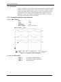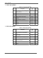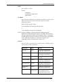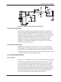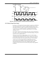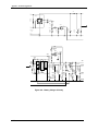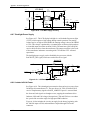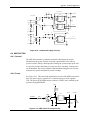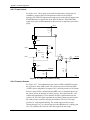
1
SERVICE MANUAL Nellcor Puritan Bennett™ NPB-3900 Patient Monitor To contact Nellcor Puritan Bennett’s representative: In the United States, call 1-800-NELLCOR or 510 463-4000; outside the United States, call your local Nellcor Puritan Bennett representative. Caution: Federal law (U. S.) restricts this device to sale by or on the order of a physician. © 1998 Nellcor Puritan Bennett Inc. All Rights Reserved 0123 047940A-0398 Corporate Headquarters Regional/Local Offices Nellcor Puritan Bennett Inc. 4280 Hacienda Drive Pleasanton, California 94588 U.S.A. Tel. 510 463-3900 or 1-800-NELLCOR Nellcor Puritan Bennett UK Ltd. 10, Talisman Business Centre London Road Bicester, Oxfordshire OX6 0JX United Kingdom Tel. +44.1869.322700 U. S. Service Repair Center Nellcor Puritan Bennett Belgium NV/SA Interleuvenlaan 62/8, Zone 2 B-3001 Heverlee Belgium Tel. +32.16.400467 Nellcor Puritan Bennett Inc. 2200 Faraday Avenue Carlsbad, California 92008 U.S.A. Tel. 619 482-5000 European Office Nellcor Puritan Bennett Europe BV Hambakenwetering 1 5231 DD ’s-Hertogenbosch The Netherlands Tel. +31.73.6485200 Asia/Pacific Office Nellcor Puritan Bennett HK Ltd. Room 1602 Evergo House 38 Gloucester Road Wanchai Hong Kong Tel. +852.2529.0363 Nellcor Puritan Bennett France 3 avenue du Canada, Bâtiment Sigma LP851 Les Ulis 91975 Courtaboeuf Cedex France Tel. +33.1.69.82.14.66 Nellcor Puritan Bennett Germany GmbH Black-&-Decker-Strasse 28 65510 Idstein Germany Tel. +49.6126.5930 Nellcor Puritan Bennett Italia S.r.L. Via Edison 6 20090 Assago (MI) Italy Tel. +39.2.4577161 Nellcor Puritan Bennett Finland Oy Kappelitie 8 02200 Espoo Finland Tel. +358.9.270.92.900 To obtain information about a warranty, if any, for this product, contact Nellcor Puritan Bennett Technical Services or your local Nellcor Puritan Bennett representative. Nellcor Puritan Bennett, Durasensor, Oxisensor II, Oxichip, C-Lock, and the Nellcor Puritan Bennett knob configuration are trademarks of Nellcor Puritan Bennett Incorporated. SureTemp is a trademark of Welch Allyn, Inc. Covered by one or more of the following U. S. Patents and foreign equivalents: 4,621,643; 4,653,498; 4,700,708; 4,770,179;,4,869,254; 4,928,692; 4,934,372; 5,078,136; 5,368,224; 5,632,555; Re.35,122. Table of Contents TABLE OF CONTENTS List of Figures List of Tables List of Figures..................................................................................................v List of Tables..................................................................................................vi Section 1: Introduction.................................................................................... 1-1 1.1 Manual Overview.................................................................................. 1-1 1.2 Warnings, Cautions, and Notes ........................................................... 1-1 1.3 NPB-3900 Patient Monitor Description ................................................ 1-1 1.4 P-3900 Introduction.............................................................................. 1-2 1.5 Related Documents.............................................................................. 1-2 Section 2: Routine Maintenance .................................................................... 2-2 2.1 Cleaning ............................................................................................... 2-2 2.2 Periodic Safety and Functional Checks ............................................... 2-2 2.3 Battery.................................................................................................. 2-2 2.4 Environmental Protection ..................................................................... 2-3 Section 3: Performance Verification .............................................................. 3-1 3.1 Introduction .......................................................................................... 3-1 3.2 Equipment Needed .............................................................................. 3-1 3.3 Performance Tests............................................................................... 3-2 3.4 Safety Tests ....................................................................................... 3-15 Section 4: Power-Up Defaults Menu and Diagnostic Mode ......................... 4-1 4.1 Introduction .......................................................................................... 4-1 4.2 Power-Up Defaults Menu ..................................................................... 4-1 4.3 Restoring Factory Settings................................................................... 4-4 4.4 Diagnostic Mode .................................................................................. 4-4 Section 5: Troubleshooting ............................................................................ 5-1 5.1 Introduction .......................................................................................... 5-1 5.2 How to use This Section ...................................................................... 5-1 5.3 Who Should Perform Repairs .............................................................. 5-1 5.4 Replacement Level Supported............................................................. 5-1 5.5 Obtaining Replacement Parts .............................................................. 5-2 5.6 Troubleshooting Guide......................................................................... 5-2 5.7 Troubleshooting the Oximetry Function ............................................. 5-11 5.8 P-3900 Troubleshooting Guide .......................................................... 5-17 Section 6: Disassembly Guide........................................................................ 6-1 6.1 Introduction .......................................................................................... 6-1 6.2 How to use This Section ...................................................................... 6-2 6.3 Disassembly Flow Charts..................................................................... 6-2 6.4 Closed Case Disassembly ................................................................... 6-7 6.5 Front Case Disassembly .................................................................... 6-16 6.6 Rear Case Disassembly..................................................................... 6-20 6.7 Main PCB Disassembly...................................................................... 6-22 Section 7: Spare Parts..................................................................................... 7-1 7.1 Introduction .......................................................................................... 7-1 7.2 Top Level Assembly............................................................................. 7-1 7.3 Front Case Assembly........................................................................... 7-2 7.4 Rear Case Assembly ........................................................................... 7-2 7.5 Main PCB Assembly ............................................................................ 7-3 iii Table of Contents 7.6 P-3900 Printer ...................................................................................... 7-4 Section 8: Packing For Shipment................................................................... 8-1 8.1 General Instructions ............................................................................. 8-1 8.2 Repacking In Original Carton ............................................................... 8-1 8.3 Repacking In a Different Carton........................................................... 8-1 Section 9: Specifications ................................................................................ 9-1 9.1 General ................................................................................................ 9-1 9.2 Safety Standards.................................................................................. 9-1 9.3 Electrical............................................................................................... 9-2 9.4 Environmental ...................................................................................... 9-2 9.5 Measuring Parameters.......................................................................... 9-2 9.6 Trends .................................................................................................. 9-7 9.7 P-3900 Printer (Optional) ..................................................................... 9-7 Section 10: RS-232 Interface......................................................................... 10-1 10.1 Serial Interface Connection.............................................................. 10-1 10.2 Nurse Call ........................................................................................ 10-1 10.3 Exporting Trend Data ....................................................................... 10-2 Appendix - Technical Supplement ..................................................................A-1 A-1 General................................................................................................A-1 A-2 Block Diagram .....................................................................................A-1 A-3 Isolated Patient Connection Section....................................................A-2 A-4 Temperature Measurement Circuit......................................................A-4 A-5 ECG Inputs ..........................................................................................A-7 A-6 On/Off Power Control ..........................................................................A-9 A-7 Audio Volume and Speaker Drive .....................................................A-11 A-8 Power Supplies..................................................................................A-12 A-9 NIBP Section .....................................................................................A-17 A-10 System A/D......................................................................................A-20 A-11 Buttons And Lights ..........................................................................A-22 A-12 SpO2 ................................................................................................A-22 A-13 Microcontroller .................................................................................A-28 A-14 Program Storage/Execution ............................................................A-32 A-15 Dram Control ...................................................................................A-33 A-16 Real Time Clock (RTC) ...................................................................A-34 A-17 Uart Operation .................................................................................A-36 A-18 FPGA Glue Logic.............................................................................A-37 iv Table of Contents LIST OF FIGURES Figure 5-1: Preamplifier and PGA Outputs ...................................................... 5-12 Figure 5-2: Filter Outputs and ADC Input ...................................................... 5-513 Figure 5-3: SpO2 Module with an SRC-2......................................................... 5-14 Figure 5-4: SpO2 Module with SRC-2 Drive Current Test at TP7.................... 5-15 Figure 5-5: SpO2 Module with SRC-2.............................................................. 5-16 Figure 6-1: Top Level Disassembly Flow Chart . 6-Error! Bookmark not defined. Figure 6-2: Front Case Disassembly Flow Chart ............................................... 6-4 Figure 6-3: Rear Case Disassembly Flow Chart................................................ 6-5 Figure 6-4: Main Board Disassembly Flow Chart .............................................. 6-6 Figure A-1: NPB-3900 Block Diagram ...............................................................A-2 Figure A-2: Temperature Measurement Circuit .................................................A-6 Figure A-3: ECG Processing Circuitry, First Stage............................................A-8 Figure A-4: ECG Processing Circuitry, Second Stage.......................................A-9 Figure A-5: Power ON/OFF Circuitry ...............................................................A-10 Figure A-6: Watchdog Circuitry........................................................................A-11 Figure A-7: Audio Volume Circuitry..................................................................A-12 Figure A-8: Buck Power Regulator, Simplified Schematic & Waveforms ........A-13 Figure A-9: Battery Charger Circuitry...............................................................A-14 Figure A-10: 3.3V Regulated Supply................................................................A-15 Figure A-11: 5V Regulated Supply Circuitry ....................................................A-15 Figure A-12: LCD Bias Supply Circuitry...........................................................A-16 Figure A-13: LCD Backlight Supply Circuitry ...................................................A-16 Figure A-14: Isolated ±5V Supply Circuitry......................................................A-17 Figure A-15: NIBP Power Sourcing Circuitry ...................................................A-17 Figure A-16: NIBP Pump Control Circuitry.......................................................A-18 Figure A-17: NIBP Pressure Sensors Processing Circuitry .............................A-19 Figure A-18: Proportional Valve Powering Circuitry.........................................A-20 Figure A-19: A/D Circuitry ................................................................................A-21 Figure A-20: Interfacing with SpO2 Processing...............................................A-23 Figure A-21: Microcontroller Signal Assignments............................................A-29 Figure A-22: Flash Timing Parameters ............................................................A-32 Figure A-23: DRAM Timing Parameters ..........................................................A-33 Figure A-24: RAS and CAS Timing..................................................................A-34 Figure A-25: Read Timing................................................................................A-35 Figure A-26: Write Timing ................................................................................A-35 Figure A-27: Data Signal..................................................................................A-37 Figure A-28: Control Signal..............................................................................A-37 Figure A-29: NPB-3900 Top Assembly Drawing (Sheet 1 of 2).......................A-43 Figure A-29: NPB-3900 Top Assembly Drawing (Sheet 2 of 2).......................A-45 Figure A-30: NPB-3900 Front Case Assembly Drawing (Sheet 1 of 2) ...........A-47 Figure A-30: NPB-3900 Front Case Assembly Drawing (Sheet 2 of 2) ...........A-49 Figure A-31: NPB-3900 Rear Case Assembly Drawing...................................A-51 Figure A-32: P-3900 Assembly Drawing..........................................................A-53 Figure A-33: NPB-3900 Interconnect Diagram ................................................A-55 Figure A-34: Main PCB Schematic Diagram (Sheet 1 of 5).............................A-57 Figure A-34: Main PCB Schematic Diagram (Sheet 2 of 5).............................A-59 Figure A-34: Main PCB Schematic Diagram (Sheet 3 of 5).............................A-61 Figure A-34: Main PCB Schematic Diagram (Sheet 4 of 5).............................A-63 Figure A-34: Main PCB Schematic Diagram (Sheet 5 of 5).............................A-65 Figure A-35: NPB-3900Patient Connector PCB Schematic Diagram..............A-67 v Table of Contents LIST OF TABLES Table 1-1: Model Configuration.......................................................................... 1-2 Table 3-1: Required Test Equipment ................................................................. 3-1 Table 3-2: SRC Settings and NBP-3900 Indications ......................................... 3-6 Table 3-3: Serial Interface Measurements....................................................... 3-13 Table 3-4: Current Test.................................................................................... 3-16 Table 3-5: Leakage Current ............................................................................. 3-16 Table 4-1: Power-Up Defaults Menu.................................................................. 4-1 Table 4-2: A/D Channel Designators ................................................................. 4-7 Table 5-1: Problem Categories .......................................................................... 5-2 Table 5-2: Power Problems ............................................................................... 5-3 Table 5-3: Serviceable Hardware Error Codes .................................................. 5-5 Table 5-4: Error Code Categories...................................................................... 5-8 Table 5-5: Buttons/Knob Problems .................................................................... 5-9 Table 5-6: Display/Audible Tones Problems...................................................... 5-9 Table 5-7: Operational Performance Problems ............................................... 5-10 Table 5-8: Fault Evaluation .............................................................................. 5-11 Table 5-9: P-3900 Troubleshooting Guide....................................................... 5-17 Table 7-1: Top Level Assembly ......................................................................... 7-1 Table 7-2: Front Case Assembly ....................................................................... 7-2 Table 7-3: Rear Case Assembly ........................................................................ 7-2 Table 7-4: Main Board Assembly....................................................................... 7-3 Table 7-5: Main PCB Jumper Configuration ...................................................... 7-3 Table 7-5: P-3900 Printer................................................................................... 7-4 Table 10-1: RS-232 Serial Interface Connections ............................................. 7-1 Table A-1: Oxichip Circuit Pin Descriptions .....................................................A-23 vi SECTION 1: INTRODUCTION 1.1 Manual Overview 1.2 Warnings, Cautions, and Notes 1.3 NPB-3900 Patient Monitor Description 1.4 P-3900 Introduction 1.5 Related Documents 1.1 MANUAL OVERVIEW This manual contains information for servicing the NPB-3900 series of patient monitors. Only qualified service personnel should service this product. Before servicing the NPB-3900, read the operator’s manual carefully for a thorough understanding of operation. 1.2 WARNINGS, CAUTIONS, AND NOTES This manual uses three terms that are important for proper operation of the monitor: Warning, Caution, and Note. 1.2.1 Warning A warning precedes an action that may result in injury or death to the patient or user. Warnings are boxed and highlighted in boldface type. 1.2.2 Caution A caution precedes an action that may result in damage to, or malfunction of, the monitor. Cautions are highlighted in boldface type. 1.2.3 Note A note gives information that requires special attention. 1.3 NPB-3900 PATIENT MONITOR DESCRIPTION The purpose and function of the NPB-3900 series of patient monitors is to monitor: ECG; heart rate; noninvasive blood pressure (systolic, diastolic, and mean arterial pressures); functional arterial oxygen saturation; and temperature for adult and pediatric patients in all hospital areas and hospital-type facilities. They may be used during hospital transport and in mobile, land-based environments, such as ambulances. Refer to the NPB-3900 operator’s manual for a description of the NPB-3900 controls, indicators, and operation. The physical and operational characteristics of the monitors are described in the operator’s manual and Section 9, Specifications, of this manual. The parameter measurements for each model in the NPB-3900 series are indicated in Table 1-1. 1-1 Section 1: Introduction Table 1-1: Model Configuration Model Parameter NIBP SpO2 NPB-3910 X X NPB-3920 X X NPB-3930 X X NBP-3940 X X TEMP ECG X X X X 1.4 P-3900 INTRODUCTION The P-3900 is an optional, standalone printer designed for use with the NPB-3900 patient monitor. The P-3900 communicates with the monitor using a null-modem cable connected between each device’s RS-232 connector. The P-3900 contains an internal battery, which, when fully charged, will operate the printer for 3 hours (typical, at 25°C, producing fifteen 20-second printouts per hour). The P-3900 can be connected to AC power using an external power supply. The P-3900 uses the same type power supply as the NPB-3900 monitor, the PS-120V or PS-240V. The P-3900 does not have an On/Off switch. The printer can sense when it has an established communications link with the monitor. At that time, the green LINKED indicator on the front panel lights, indicating that the printer is ready for operation. See the NPB-3900 operator’s manual for more information regarding use of the printer. 1.5 RELATED DOCUMENTS To perform test and troubleshooting procedures and to understand the principles of operation and circuit analysis sections of this manual, you must know how to operate the monitor. Refer to the NPB-3900 operator’s manual. To understand the various Nellcor Puritan Bennett sensors, ECG leads, blood pressure cuffs, and temperature probes that work with the monitor, refer to the operator’s manual and individual directions for use that accompany these accessories. 1-2 SECTION 2: ROUTINE MAINTENANCE 2.1 Cleaning 2.2 Periodic Safety and Functional Checks 2.3 Battery 2.4 Environmental Protection 2.1 CLEANING WARNING: Do not spray, pour, or spill liquid on the NBP-3900, its accessories, connectors, switches, or openings in the chassis. Do not immerse the NPB-3900 or its accessories in liquid or clean with caustic or abrasive cleaners. To clean the NPB-3900, dampen a cloth with a commercial, nonabrasive cleaner and wipe the exterior surfaces lightly. Do not allow any liquids to come in contact with the power connector or switches. Do not allow any liquids to penetrate connectors or openings in the instrument. For cables, sensors, and cuffs, follow the cleaning instructions in the directions for use that accompany these accessories. 2.2 PERIODIC SAFETY AND FUNCTIONAL CHECKS Nellcor Puritan Bennett recommends that the following checks be performed at least every 2 years by a qualified service technician. 1. Inspect the exterior of the NPB-3900 for damage. 2. Inspect labels for legibility. If the labels are not legible, contact Nellcor Puritan Bennett’s Technical Services Department or your local Nellcor Puritan Bennett representative. 3. Verify that the unit performs properly as described in paragraph 3.3. 4. Perform the electrical safety tests detailed in paragraph 3.4. If the unit fails these electrical safety tests, do not attempt to repair. Contact Nellcor Puritan Bennett’s Technical Services Department or your local Nellcor Puritan Bennett representative. 2.3 BATTERY If the NPB-3900 has not been used for a long period of time, the battery will need charging. To charge the battery, connect the NPB-3900 to an AC source as described in the Setup & Use section of the operator’s manual. NOTE: Storing the NBP-3900 for a long period without charging the battery may degrade the battery capacity. A complete battery recharge when not using the monitor requires 8 hours. The battery may be recharged while the monitor is in use; in which case, the battery will require 14 hours to be recharged. The battery may require a full charge/discharge cycle to restore normal capacity. 2-1 Section 3: Performance Verification Nellcor Puritan Bennett recommends that the NPB-3900’s sealed, lead-acid battery be replaced at 2-year intervals. Refer to Section 6, Disassembly Guide. 2.4 ENVIRONMENTAL PROTECTION Follow local governing ordinances and recycling plans regarding disposal or recycling batteries and other device components. 2-3 SECTION 3: PERFORMANCE VERIFICATION 3.1 Introduction 3.2 Equipment Needed 3.3 Performance Tests 3.4 Safety Tests 3.1 INTRODUCTION This section discusses the tests used to verify performance following repairs or during routine maintenance. All tests can be performed without removing the NPB-3900 covers. If the NPB-3900 fails to perform as specified in any test, repairs must correct the problem before the monitor is returned to the user. 3.2 EQUIPMENT NEEDED Table 3-1 lists the equipment required for performance verification. Table 3-1: Required Test Equipment Equipment Description Digital multimeter (DMM) Fluke Model 87 or equivalent Sensor extension cable EC-8 Durasensor® finger clip sensor DS-100A Oxisensor® II adhesive sensor D-25 ECG cable CE-10 ECG electrodes Standard ECG leads LE series NIBP hose SHBP-10 NIBP cuff SCBP series Temperature probe Welch Allyn SureTemp® (blue capped probe) Pulse oximeter tester Nellcor Puritan Bennett SRC-2 ECG simulator Dynatech Nevada medSim 300 or equivalent NIBP simulator Bio-Tek “BP Pump” or equivalent Thermometer Calibrator Key Welch Allyn Model 767 Safety analyzer Bio-Tek 601 Pro or equivalent Stopwatch Manual or electronic 3-1 Section 3: Performance Verification 3.3 PERFORMANCE TESTS The battery charge and battery performance tests should be performed before monitor repairs whenever the battery is suspected as being a source of a problem. All other tests should be performed following monitor repairs. Before performing the battery performance test, ensure that the battery is fully charged (paragraph 3.3.1). This section is written using Nellcor Puritan Bennett factory-set power-up defaults. If your institution has reconfigured custom defaults, those values will be displayed. 3.3.1 Battery Charge Perform the following procedure to fully charge the battery. 1. Connect the monitor to an AC power source using the PS-120 or PS-240 external power supply and power cord, if needed. 2. Verify that the EXTERNAL POWER indicator is lit. 3. Charge the battery for at least 8 hours. The battery may require a complete charge/discharge cycle to restore its normal capacity. 4. To check for a full charge, perform the procedure in paragraph 3.3.2 “Battery Performance Test.” 3.3.2 Battery Performance Test The monitor is specified to operate typically on battery power for a minimum of 4 hours, at 25°C, with one NIBP measurement every 15 minutes. Before performing this test, ensure that the battery is fully charged (paragraph 3.3.1). 3- 2 1. Connect the Nellcor Puritan Bennett SRC-2 pulse oximeter tester to the monitor via the EC-8 sensor cable. Connect the NIBP simulator to the monitor via the SHBP-10 hose. 2. Set the SRC-2 switches as follows: SWITCH POSITION RATE 38 LIGHT LOW MODULATION LOW RCAL/MODE RCAL 63/LOCAL 3. Set the NIBP simulator to simulate a pressure setting of 120/80 mmHg and heart rate of 80 bpm. 4. Ensure that the monitor is not connected to AC power. Section 3: Performance Verification 5. With the NPB-3900 turned off, press the ON/STANDBY button and verify that the battery icon appears at the bottom of the display after the power-on self-test is completed. The boxes in the battery icon should all be filled, indicating the battery is charged. 6. Verify that the monitor is responding to the SpO 2 simulator signal and that the audible alarm is sounding. Use the knob to select the SpO 2 Menu and permanently silence the SpO2 audible alarm. 7. Use the knob to select the NIBP Menu and set the Automatic Measurement Interval to 15 minutes. Exit the menu and press the front panel NIBP button to manually initiate the first NIBP measurement. Subsequent NIBP measurements will be taken automatically every 15 minutes. 8. The monitor must operate for at least 4 hours before the monitor automatically powers down due to low battery condition. 9. Verify that the low battery alarm occurs 15-30 minutes before the battery fully discharges. 10. Allow the monitor to operate until it automatically powers down due to low battery condition. Verify that an audible alarm sounds when the monitor automatically shuts down. Press the alarm silence button to terminate this audible alarm. 11. If the monitor passes this test, immediately recharge the battery (paragraph 3.3.1, steps 1–3). 3.3.3 Power-On Self-Test 1. Connect the monitor to an AC power source using the PS-120 or PS-240 power supply and power cord, and verify that the EXTERNAL POWER indicator is lit. 2. Do not connect any input cables to the monitor. 3. Observe the monitor front panel. With the monitor off, press the ON/STANDBY button. The monitor must perform the following sequence. a. The monitor emits a beep. b. A few seconds later, the display backlight illuminates, but the display is blank. c. The Nellcor Puritan Bennett logo then appears for a few seconds, with the version numbers of the boot and operational software displayed in the lower left corner of the display. (The upper version number corresponds to the boot software, the lower version number corresponds to the operational software.) d. A beep signals the end of the power-on self-test. The power-on selftest takes approximately 10 seconds to complete. e. Upon successful completion of the power-on self-test, the display will be in the normal monitoring screen configuration. No vital-sign numeric values or trend values will be displayed. 3-3 Section 3: Performance Verification 3.3.4 Hardware and Software Tests Hardware and software testing includes the following tests applicable to the indicated models in the series. • 3.3.4.1 SpO2 Testing NPB-3900 • 3.3.4.2 Operation with an ECG Simulator — NPB-3930, NPB-3940 • 3.3.4.3 Verification of Pneumatic System — NPB-3900 • 3.3.4.4 Operation with a Temperature Simulator — NPB-3920, NPB-3940 • 3.3.4.5 General Operation — NPB-3900 3.3.4.1 SpO2 Testing (NPB-3900) SpO2 testing includes the following tests. • 3.3.4.1.1 Alarms and Alarm Silence • 3.3.4.1.2 Heart Rate Tone Volume Control • 3.3.4.1.3 Dynamic Operating Range • 3.3.4.1.4 LED Excitation Test 3.3.4.1.1 Alarms and Alarm Silence 1. 2. Connect the SRC-2 pulse oximeter tester to the EC-8 sensor extension cable and connect the cable to the monitor. Set the SRC-2 as follows: SWITCH POSITION RATE 38 LIGHT LOW MODULATION OFF RCAL/MODE RCAL 63/LOCAL Press the ON/STANDBY button to turn the monitor on. After the normal power-up sequence, verify that the SpO2% display initially indicates zero or is blank. NOTE: The pulse bar may occasionally indicate a step change as the monitor is in the pulse search mode. 3. Move the modulation switch on the SRC-2 to LOW. 4. Verify the following monitor reaction: a. The pulse bar begins to track the artificial pulse signal from the SRC-2. 3- 4 b. Initially, zero is displayed in the SpO2 frame, or it is blank. c. After about 10 to 20 seconds, the monitor displays saturation and heart rate as specified by the tester. Verify that the values are within the following tolerances: Oxygen Saturation Range 79% to 83% Heart Rate Range 35 to 41 bpm Section 3: Performance Verification d. The audible alarm sounds and both the SpO2% and HEART RATE displays flash, indicating both parameters have violated the default alarm limits. e. The heart rate tone is heard. (Heart rate tone source, found in the Heart Rate Menu, should be set to “SpO 2”.) 5. Press the ALARM SILENCE button on the front panel of the monitor. The audible alarm is temporarily silenced. 6. Verify the following: a. The audible alarm remains silenced. b. The “slashed bell” icon appears in each numeric frame on the display. c. The SpO2% and HEART RATE displays continue flashing. d. The heart rate tone remains audible. e. The audible alarm returns in approximately 60 seconds. 3.3.4.1.2 Heart Rate Tone Volume Control Connect the SRC-2 pulse oximeter tester to the EC-8 sensor extension cable and connect the cable to the monitor. Set the SRC-2 as follows: SWITCH POSITION RATE 38 LIGHT LOW MODULATION LOW RCAL/MODE RCAL 63/LOCAL 1. Power on the monitor and verify that the SpO2 and heart rate values are correctly displayed. Press the ALARM SILENCE button on the front panel of the monitor to temporarily silence the audible alarm. 2. Verify that the heart rate tone source, found in the Heart Rate Menu, is set to “SpO2”. Press the VOLUME button on the front panel of the monitor. Within 3 seconds of having pressed the button, rotate the knob CW and verify that the beeping heart rate tone sound level increases. 3. Rotate the knob CCW and verify that the beeping heart rate tone decreases until it is no longer audible. Rotate the knob CW to return the beep volume to a comfortable level. (Note that 3 seconds after the last button-press or rotation of the knob, function of the knob reverts to moving the highlight on the display screen.) 3-5 Section 3: Performance Verification 3.3.4.1.3 Dynamic Operating Range The following test sequence verifies proper monitor operation over a range of input signals. 1. Connect the SRC-2 to the NPB-3900 (using an EC-8) and turn the NPB-3900 on. 2. Place the SRC-2 in the RCAL 63/LOCAL mode. 3. Set the SRC-2 as indicated in Table 3-2. Verify that the NPB-3900 readings are within the indicated tolerances. Allow the monitor several seconds to stabilize the readings. NOTE: A “*” indicates values that produce an alarm. Press the ALARM SILENCE button to temporarily silence the audible alarm. Table 3-2: SRC Settings and NBP-3900 Indications SRC-2 Settings RATE 38 112 201 201 LIGHT HIGH2 HIGH1 LOW LOW MODULATION LOW HIGH LOW HIGH NPB-3900 Indications SpO2 79 - 83* 79 - 83* 79 - 83* 79 - 83* Pulse Rate 35 - 41* 109 - 115 195 - 207* 195 - 207* NOTE: For the pulse rate setting of 201 bpm, the pulse rate tolerance of 195 to 207 bpm is greater than the ±3 bpm accuracy specification of the monitor, due to the performance characteristics of the SRC-2 tester. 4. Turn the monitor off. 3.3.4.1.4 LED Excitation Test This procedure uses normal system components to test circuit operation. A Nellcor Puritan Bennett Oxisensor II adhesive sensor, model D-25, is used to examine LED intensity control. The red LED is used to verify intensity modulation caused by the LED intensity control circuit. 3- 6 1. Connect an EC-8 sensor extension cable to the monitor. 2. Connect a D-25 sensor to the sensor extension cable. 3. Press the ON/STANDBY button to turn the monitor on. 4. Leave the sensor open with the LED and photodetector visible. 5. After the monitor completes its normal power-up sequence, verify that the sensor LED is brightly lit. Section 3: Performance Verification 6. Slowly move the sensor LED in proximity to the photodetector element of the sensor. Verify, as the LED approaches the optical sensor, that the LED intensity decreases. 7. Open the sensor and notice that the LED intensity increases. 8. Repeat step 6 and the intensity again decreases. This variation is an indication that the microprocessor is in proper control of LED intensity. 9. Turn the NPB-3900 off. 3.3.4.2 Operation with an ECG Simulator (NPB-3930, NPB-3940) 1. 2. With the monitor off, connect the ECG leads to the appropriate jacks on the ECG tester. Connect the leads to the CE-10 ECG cable. Connect the CE-10 to the ECG input port on the NPB-3900. Set the ECG tester as follows: Heart rate: 30 bpm Amplitude: 1 millivolt Lead select: II Normal sinus rhythm Adult mode NOTE: The accuracy of the monitor’s ECG measurements is ±5 bpm. In the procedure below, add the tolerance of the simulator to the acceptable range of readings. 3. Press the ON/STANDBY button to turn the monitor on. After the normal power-up sequence, verify the following monitor reactions: a. After at least five heartbeats, the monitor displays a heart rate of 30 ±5 bpm. b. The audible alarm sounds and the HEART RATE display flashes, indicating the heart rate is below the default lower alarm limit. 4. Press the ALARM SILENCE button. Verify that the audible alarm is silenced. 5. Increase the heart rate setting on the ECG simulator to 240 bpm. 6. After at least five heartbeats, verify that the monitor displays a heart rate of 240 ±5 bpm. 7. Verify that the audible alarm sounds and the HEART RATE display flashes, indicating that the heart rate is above the default upper alarm limit. 8. Press the ALARM SILENCE button to silence the alarm. 3-7 Section 3: Performance Verification 9. Decrease the heart rate setting on the ECG simulator to 120 bpm. 10. After at least five heartbeats, verify that the monitor displays a heart rate of 120 ±5 bpm. 11. Disconnect the LL lead from the ECG simulator. Verify that the “Leads Off” alarm message appears, three dashes are displayed in the HEART RATE display, and a low priority audible alarm sounds. 12. Reconnect the LL lead to the ECG simulator. Verify that the “Leads Off” alarm message no longer appears and that the audible alarm is silenced. 13. Repeat steps 11 and 12 for the LA and RA leads. 14. Turn the monitor off. 3.3.4.3 Verification of Pneumatic System (NPB-3900) Tests in paragraphs 3.3.4.3.1 through 3.3.4.3.5 verify the functionality of the NPB-3900 pneumatic system. These tests were designed to use the Bio-Tek “BP Pump” noninvasive blood pressure simulator. The internal test volume of the Bio-Tek simulator is 250 cm , which is used to calculated the inflation/deflation rate periods. The Bio-Tek simulator, or any equivalent NIBP simulator, is required to perform these tests. 3 The NPB-3900 must be placed in Diagnostic Mode, with the NIBP Test screen active for each of the NIBP tests. For a detailed explanation of the Diagnostic Mode, refer to Section 4, Power-up Defaults Menu and Diagnostic Mode. Each of the tests described in paragraphs 3.3.4.3.1 through 3.3.4.3.5 must be performed to verify pneumatic system functionality. These tests can be performed individually (in any order) or sequentially. Prior to performing any of these tests, perform the following setup procedure. If these tests are performed in sequence, this procedure needs to be performed once prior to the first test. 1. Turn on the Bio-Tek simulator and press the MODE button to place the simulator in test mode. The simulator screen will indicate “Internal Cuff” and “Pressure Gauge”. 2. Connect the simulator hose to the NIBP connector on the NPB-3900. 3. Follow the procedure described in Section 4 to place the NPB-3900 in Diagnostic Mode with the NIBP Test screen active. 3.3.4.3.1 Pressure Transducer Accuracy The pressure transducer accuracy test verifies the pressure accuracy of the NBP-3900 pressure transducer. 3- 8 Section 3: Performance Verification 1. Confirm that the Bio-Tek simulator is in test mode. The simulator should display “Pressure Gauge”. Confirm that the simulator is set up for the internal cuff. 2. Confirm that the NIBP Test screen is active on the NPB-3900. Press, then release, the SPEAKER button on the NPB-3900 to verify that the valve is closed. 3. Press the CONTRAST button on the NPB-3900, then the ZERO button on the simulator, to perform an offset adjustment so that the simulator and NBP-3900 both display a pressure of 0 mmHg. 4. Press the SELECT button on the simulator until the simulator displays “Pressure Source Set Test Pressure”. Use the UP/DOWN buttons on the simulator to adjust for 250 mmHg. 5. Press the START PUMP button on the simulator. The simulator will begin to pressurize. The current pressure in mmHg is displayed on both the simulator and NPB-3900 displays. 6. Allow 15-20 seconds for the pressure to stabilize. The pressure displayed on the NPB-3900 and the simulator should be within 5 mmHg of one another to complete the test successfully. 7. Press the STOP PUMP button on the simulator to stop the test. 8. Press and hold the SPEAKER button until the NPB-3900 displays a pressure of 0 mmHg. 9. Additional NIBP tests may be performed at this time. If no further NIBP tests are to be conducted, turn the NPB-3900 off. Normal monitoring operation will return the next time the monitor is turned on. 3.3.4.3.2 Pneumatic Leakage The pneumatic leakage test verifies the integrity of the pneumatic system. A timer/stopwatch is required for this test. 1. Ensure that the Bio-Tek simulator is in test mode. The simulator should display “Pressure Gauge”. Confirm that the simulator is set up for the internal cuff. 2. Ensure that the NIBP Test screen is active on the NPB-3900. Press, then release, the SPEAKER button on the NPB-3900 to verify that the valve is closed. 3. Press the CONTRAST button on the NPB-3900, then the ZERO button on the simulator, to perform an offset adjustment so that the simulator and NBP-3900 both display a pressure of 0 mmHg. 3-9 Section 3: Performance Verification 4. Press the NIBP button on the NPB-3900 to activate the pump. Hold the button until the NPB-3900 displays a pressure of approximately 250 mmHg. Allow 15-20 seconds for the pressure to stabilize. Record the pressure displayed on the monitor, and initiate a 1-minute timer. After 1 minute, again record the pressure displayed. The test is successfully completed if the pressure has dropped by 6 mmHg, or less, during the 1-minute period. 5. Press and hold the SPEAKER button until the NPB-3900 displays a pressure of 0 mmHg. 6. Additional NIBP tests may be performed at this time. If no further NIBP tests are to be conducted, turn the NPB-3900 off. Normal monitoring operation will return the next time the monitor is turned on. 3.3.4.3.3 Inflation Rate The inflation rate test verifies the inflation rate of the NPB-3900. A timer/stopwatch is required for this test. 1. Ensure that the Bio-Tek simulator is in test mode. The simulator should display “Pressure Gauge”. Confirm that the simulator is set up for the internal cuff. 2. Ensure that the NIBP Test screen is active on the NPB-3900. Press, then release, the SPEAKER button on the NPB-3900 to verify that the valve is closed. 3. Press the CONTRAST button on the NPB-3900, then the ZERO button on the simulator, to perform an offset adjustment so that the simulator and NBP-3900 both display a pressure of 0 mmHg. 4. Press the NIBP button on the NPB-3900 to activate the pump, and simultaneously start the timer. Hold the NIBP button until the monitor displays a pressure of 280 mmHg. When a pressure of 280 mmHg is reached, stop the timer. The test is successfully completed if the inflation time is between 1 and 6 seconds. 5. Press and hold the SPEAKER button until the NPB-3900 displays a pressure of 0 mmHg. 6. Additional NIBP tests may be performed at this time. If no further NIBP tests are to be conducted, turn the NPB-3900 off. Normal monitoring operation will return the next time the monitor is turned on. 3.3.4.3.4 Deflation Rate The deflation rate test verifies the deflation rate of the NPB-3900. A timer/stop watch is required for this test. 1. Ensure that the Bio-Tek simulator is in test mode. The simulator should display “Pressure Gauge”. Confirm that the simulator is set up for the internal cuff. 3- 10 Section 3: Performance Verification 2. Ensure that the NIBP Test screen is active on the NPB-3900. Press, then release, the SPEAKER button to verify that the valve is closed. 3. Press the CONTRAST button on the NPB-3900, then the ZERO button on the simulator, to perform an offset adjustment so that the simulator and NBP-3900 both display a pressure of 0 mmHg. 4. Press the NIBP button on the NPB-3900 to activate the pump. Hold the button until the NPB-3900 displays a pressure of 280 mmHg. Initiate a 1-minute timer, and simultaneously press and hold the ALARM SILENCE button on the NPB-3900. This will cause the pneumatic system to deflate at a rate of 3 mmHg/sec ±1.5 mmHg/sec. After 1 minute, record the pressure displayed on the NPB-3900. The test is successfully completed if the monitor displays a pressure reading of 10 mmHg to 190 mmHg. 5. Press and hold the SPEAKER button until the NPB-3900 displays a pressure of 0 mmHg. 6. Additional NIBP tests may be performed at this time. If no further NIBP tests are to be conducted, turn the NPB-3900 off. Normal monitoring operation will return the next time the monitor is turned on. 3.3.4.3.5 Over-pressure The over-pressure test verifies the functionality of the over-pressure relief system of the NPB-3900. 1. Ensure that the Bio-Tek simulator is in test mode. The simulator should display “Pressure Gauge”. Confirm that the simulator is set up for the internal cuff. 2. Ensure that the NIBP Test screen is active on the NPB-3900. Press, then release, the SPEAKER button on the NPB-3900 to verify that the valve is closed. 3. Press the CONTRAST button on the NPB-3900, then the ZERO button on the simulator, to perform an offset adjustment so that the simulator and NBP-3900 both display a pressure of 0 mmHg. 4. Press the SELECT button on the simulator until the simulator displays “Overpressure Test”. Press the START TEST button on the simulator. The simulator will pressurize the system until the monitor’s over-pressure relief system activates, including the warning display screen. The simulator will display the pressure value that caused the NPB-3900 over-pressure relief system to activate. The test is successfully completed if the simulator displays a pressure reading of 280 mmHg to 330 mmHg. 5. Press and hold the SPEAKER button to ensure that the NPB-3900 displays a pressure of 0 mmHg. 6. Additional NIBP tests may be performed at this time. If no further NIBP tests are to be conducted, turn the NPB-3900 off. Normal monitoring operation will return the next time the monitor is turned on. 3-11 Section 3: Performance Verification 3.3.4.4 Operation with a Thermometer Calibration Key (Models 3920 and 3940) 1. Remove the probe from its holder. 2. Insert the calibration key in the temperature input port T on the NPB-3900. 3. Press the ON/STANDBY button to turn the monitor on. After the normal power-up sequence, verify that the temperature reads 36.3 ±0.1 °C (or 97.3 ±0.2 °F). 4. Turn the monitor off. 3.3.4.5 General Operation The following tests provide an overall performance check of the system: • 3.3.4.4.1 Operation with a Human Subject • 3.3.4.4.2 Serial Interface Test • 3.3.4.4.3 Printer Verification 3.3.4.5.1 Operation with a Human Subject Patient monitoring involves connecting the monitor to a human subject for a qualitative test. 3- 12 1. Connect an EC-8 sensor extension cable to the monitor. Connect a Nellcor Puritan Bennett Durasensor finger clip sensor, model DS-100A, to the sensor extension cable. Clip the DS-100A to the subject as described in the sensor directions for use. 2. Connect a CE-10 ECG cable to the NPB-3930 or NPB-3940. Connect ECG leads to the cable. Connect ECG electrodes to the leads. Apply ECG electrodes to the subject according to the lead’s and electrodes’ directions for use. 3. Connect an SHBP-10 blood pressure hose to the monitor. Apply the appropriate SCBP series blood pressure cuff to the subject according to the cuff directions for use. 4. Connect a blue-capped SureTemp oral thermometer probe to the NPB-3920 or NPB-3940. Place the probe in its holder in the module on the rear of the monitor. 5. Press the ON/STANDBY button to turn the monitor on and verify that the monitor is operating. 6. The monitor should stabilize on the subject’s physiological signals in about 15 to 30 seconds. Verify that the saturation and heart rate are reasonable for the subject. 7. Press the NIBP button on the front panel of the monitor. Verify that the blood pressure values are reasonable for the subject. Section 3: Performance Verification 8. Remove the temperature probe from its holder. Following the directions in the NPB-32900 operator’s manual, apply a new probe cover and take the subject’s temperature. Verify that the temperature measurement is reasonable for the subject. 3.3.4.5.2 Serial Interface Test RS-232 Perform the following procedure to test the serial port voltages. The test is qualitative and only verifies that the serial interface port is powered correctly, and that the “nurse call” signal is operational. The serial connector is a male DB-9 located on the monitor’s rear panel, identified with the RS-232 symbol. 1. Turn the monitor ON. 2. Set up the DMM with the function set to “VDC” at a range of 10 volts. 3. Connect the DMM negative lead to connector pin 5 (GND), or the shell of the RS-232 connector. 4. Connect the DMM positive lead to the following pins, in turn, and verify the voltage values listed in Table 3-3. (Voltage for pin 9 is that listed for the “no alarm” condition.) Table 3-3: Serial Interface Measurements Pin 1 2 3 4 5 6 7 8 9 9 Signal not used RXD <<< TXD >>> DTR >>> GND DSR <<< RTS >>> CTS <<< Alarm Out >>> (no alarm) Alarm Out >>> (alarm underway) Measurement (V) Min Typical Max -0.4 0.0 0.4 -0.4 0.0 0.4 -5.0 -9.0 -15.0 -5.0 -9.0 -15.0 -0.4 0.0 0.4 -0.4 0.0 0.4 -5.0 -9.0 -15.0 -0.4 0.0 0.4 -5.0 -9.0 -15.0 5.0 9.0 15.0 5. Connect the Nellcor Puritan Bennett SRC-2 pulse oximeter tester to the monitor via the EC-8 sensor extension cable. 3-13 Section 3: Performance Verification 6. Set the SRC-2 switches as follows: SWITCH POSITION RATE 38 LIGHT LOW MODULATION LOW RCAL/MODE RCAL 63/LOCAL 7. Verify that the monitor is responding to the SpO 2 simulator signal and the audible alarm is sounding. If desired, press the ALARM SILENCE button to temporarily silence the audible alarm. 8. Connect the DMM positive lead to pin 9 and verify the voltage value listed in Table 3-3. (Voltage for pin 9 is that listed for the “alarm underway” condition.) 3.3.4.5.3 Printer Verification (For Optional Printer) Printer verification consists of connecting the printer to the monitor and the monitor to a human subject for a qualitative test. 15V - 1A RS-232 1. Connect the output of the appropriate power supply, PS-240V or PS-120V, to the labeled connector in the rear of the printer. When the printer’s external power supply is connected, the printer front-panel charging LED is lighted. 2. Connect the serial cable between the labeled connectors in the rear panels of the monitor and the printer. 3. The printer front-panel communication LED is lighted when the RS-232 communications link is completed. 4. Rotate the monitor knob to highlight the setup icon . Press the knob and ensure Communications Selection is (Printer). 5. Connect an EC-8 sensor extension cable to the monitor. Connect a Nellcor Puritan Bennett Durasensor oxygen transducer, model DS-100A, to the sensor extension cable. Attach the DS-100A to the subject as described in the sensor directions for use. 6. Press the ON/STANDBY button to turn the monitor on and verify that the monitor is operating. 7. The monitor should stabilize on the subject’s physiological signal in about 15 to 30 seconds. Verify that the saturation and heart rate is reasonable for the subject. 3- 14 Section 3: Performance Verification 8. Press the printer CONTINUOUS BUTTON. Verify that the printout contains vital signs across the top of the paper, and that aSpO 2 waveform, with grid marks, occupies the center portion of the paper. Press the CONTINUOUS BUTTON again to terminate printout. 9. Disconnect the sensor and shut off the monitor. 3.4 SAFETY TESTS NPB-3900 safety tests consist of the following Leakage Currents elements, performed in accordance with IEC 601-1. 3.4.1 Protective Ground Continuity NOTE: The NPB-3900 does not require an isolated Earth Ground terminal, neither is one installed. No Protective Ground Continuity check is required. 3.4.2 Electrical Leakage NPB-3900 leakage current tests consist of the following elements, performed in accordance with IEC 601-1, clause 19: • Patient Leakage Current • Patient Leakage Current, with Mains Voltage on the Applied Part 3.4.2.1 Patient Leakage Current This test measures patient leakage current in accordance with IEC 601-1, clause 19, for Class II, type CF equipment. Patient leakage current in this test is measured from any individual patient connection to earth (power ground). NOTE: This test requires a test cable for each patient connector. For example, the ECG test cable consists of the ECG cable connector, with all the conductors shorted together, connected to a test lead from the electrical safety analyzer. Test cables for SpO2 and temperature can be configured in a similar manner. 1. Configure the electrical safety analyzer as recommended by the analyzer operating instructions. 2. Connect the appropriate external power supply input power cord to the analyzer as recommended by the analyzer operating instructions. Connect the external power supply output cord to the monitor. 3. Connect the ECG test cable to the ECG connector on the NPB-3930 /3940 and the appropriate input connector on the analyzer. Turn on the NPB-3930/3940. 4. Perform the test as recommended by the analyzer operating instructions. Patient leakage current is measured under various conditions of the AC mains. For each condition, the measured leakage current must not exceed that indicated in Table 3-4. 3-15 Section 3: Performance Verification 5. Repeat the test for the SpO 2 and temperature patient connections, using the appropriate test cables. Table 3-4: Current Test Test Condition Allowable Leakage Current (milliamps) Normal polarity 0.01 Normal polarity; Neutral (L2) open 0.05 Reverse polarity 0.01 Reverse polarity; Neutral (L2) open 0.05 3.4.1.3 Patient Leakage Current, with Mains Voltage on the Applied Part This test measures patient leakage current in accordance with IEC 601-1, clause 19, for Class II, type CF equipment. In this test, 110% of mains voltage is applied between each patient connection and earth (power ground). Patient leakage current is then measured from any individual patient connection to earth. NOTE: This test requires the same test cables for each patient connector as described in section 3.4.1.2. WARNING: AC mains voltage will be present on the applied part terminals during this test. Exercise caution to avoid electrical shock hazard. 1. Configure the electrical safety analyzer as recommended by the analyzer operating instructions. 2. Connect the monitor’s appropriate external power supply input power cord to the analyzer as recommended by the analyzer operating instructions. Connect the external power supply output cord to the monitor. 3. Connect the ECG test cable to the ECG connector on the NPB-3930/3940 and the appropriate input connector on the analyzer. Turn on the NPB-3930/3940. 4. Perform the test as recommended by the analyzer operating instructions. Patient leakage current is measured with normal and reverse mains polarity. For each condition, the measured leakage current must not exceed that indicated in Table 3-5. 5. Repeat the test for the SpO 2 and temperature patient connections, using the appropriate test cables. Table 3-5: Leakage Current Allowable Leakage Test Condition Current (milliamps) Normal polarity 0.05 Reverse polarity 0.05 3- 16 SECTION 4: POWER-UP DEFAULTS MENU AND DIAGNOSTIC MODE 4.1 Introduction 4.2 Power-up Defaults Menu 4.3 Restoring Factory Settings 4.4 Diagnostic Mode 4.1 INTRODUCTION This section discusses use of the Power-up Defaults Menu to configure power-on default settings, and the Diagnostic Mode to obtain service-related information about the monitor. 4.2 POWER-UP DEFAULTS MENU The purpose of the Power-up Defaults Menu (Table 4-1) is to allow the authorized user to create a “power-up default” for each setting in the NPB-3900. Power-up defaults are the settings in effect each time the NPB-3900 is powered on. Once the Power-up Defaults Menu is entered, physiological monitoring is terminated. The screen layouts do NOT display any information associated with normal monitoring operation. Use the following procedure to configure the power-up default settings for the NPB-3900 monitor. 1. While in normal monitoring mode, adjust each accessible setting on the monitor as desired, using the techniques described in the operator’s manual. Such settings include alarm limits, choice of display type for the graphic frame, and ECG lead select. 2. Use the knob to invoke the Set-up Menu (choose the screwdriver icon found along the bottom of the display). 3. Select the menu item “Enter Power-Up Defaults Menu”. Once selected, a pop-up box appears with the text “Enter 3-Digit Passcode”. Use the knob to enter the passcode, 2 1 5. This passcode is set at the factory and may not be changed. 4. The Power-up Defaults Menu is now present. The available menu items are explained in the table that follows. Make changes to these menu items as desired. Table 4-1: Power-Up Defaults Menu MENU ITEM* Accept Current Settings? CHOICES** “Yes” “No” EXPLANATION If “Yes” is chosen, the current NPB-3900 settings become the power-up defaults. 4-1 Section 4: Power-up Defaults Menu and Diagnostic Mode Table 4-1: Power-Up Defaults Menu - (Continued) MENU ITEM* CHOICES** Permanent Audible “Make Available” Alarm Silence “Deny Access” If “Make Available” is chosen, the caregiver may permanently silence the audible alarm for a particular parameter via the Alarm/Limits Menu. Some institutions may wish to prevent audible alarms from being permanently silenced. If so, “Deny Access” should be selected. Alarm Suspend If “Make Available” is chosen, the caregiver may invoke the Alarm Suspend Mode by pressing and holding the Alarm Silence button for 2 seconds. Some institutions may wish to prevent Alarm Suspend from being invoked. If so, “Deny Access” should be selected. “Make Available” “Deny Access” Auto-Set Limits “Make Available” “Deny Access” 4-2 EXPLANATION If “Make Available” is chosen, the caregiver may invoke the Auto-Set Limits function via the Alarm/Limits Menu. Some institutions may wish to prevent Auto-Set Limits from being invoked. If so, “Deny Access” should be selected. Section 4: Power-up Defaults Menu and Diagnostic Mode Table 4-1: Power-Up Defaults Menu - (Continued) MENU ITEM* Language CHOICES** “English” “Français” “Deutsch” “Español” EXPLANATION The language selected will be used for all the text shown on the display; the selected language will be effective the next time the monitor is powered up. “Italiano” “Portugués” “Japanese” “Chinese” “Russian” Enter Diagnostic Mode “Yes” “No” Done If “Yes” is chosen, the Powerup Defaults Menu is exited and the Diagnostic Menu appears. When selected, the Power-up Defaults Menu is immediately exited and the user is instructed to power down the monitor. * The choice in effect at the time the screen is accessed is shown in parentheses following the menu item. ** Bold type indicates the choice when the factory-set default menu appears. The highlighting is displayed in reverse video. 5. After making any desired changes to the menu items, choose the menu item “Accept current settings?”, select “YES”, then select “Done”. 6. Upon selecting “Done”, a Notice screen will appear, with the directions that the monitor must be powered off, and that any changes made to the power-up defaults will be in effect next time the unit is powered up. 4-3 Section 4: Power-up Defaults Menu and Diagnostic Mode NOTICE Turn off the monitor at this time. Any changes made to the power-up defaults will be in effect the next time the monitor is turned on. 4.3 RESTORING FACTORY SETTINGS CAUTION: In addition to restoring factory defaults, this procedure will also clear the contents of trend memory. NOTE: Read this procedure completely before performing the first step. The following technique can be used to restore the monitor’s power-up default settings which were originally established at the factory: 1. With the monitor powered off, simultaneously press the Volume and Contrast buttons on the front keypad. 2. While continuing to press the Volume and Contrast buttons, power-up the monitor. 3. Continue to keep the Volume and Contrast buttons depressed until the power-up diagnostic sequence is complete. When the normal monitoring screen appears, release the two buttons. 4.4 DIAGNOSTIC MODE The purpose of Diagnostic Mode is to allow factory, field-service, and hospital biomedical technicians access to a series of test and system-related information screens for the purpose of verifying NPB-3900 performance or troubleshooting problems. To access the Diagnostic Mode, first invoke the Power-up Defaults Menu as described in section 4.2. Then, select the menu item, “Enter Diagnostic Mode”. Choose “Yes”. The Power-up Defaults Menu will be exited and the Diagnostic Menu will appear. 4-4 Section 4: Power-up Defaults Menu and Diagnostic Mode DIAGNOSTIC MENU Error Codes System Information System A/D Values NIBP Test Return The Diagnostic Menu lists the test and system-related information screens. Selection of an item in the menu will invoke that test or information screen. The test and information screens that appear in the Diagnostic Menu are as follows: • Error Codes • System Information • System A/D Values • NIBP Test • Return 4.4.1 Error Codes This screen displays the 10 most recent error code types, logged by the NPB-3900. After 10 error code types have been logged, the oldest error code type will be deleted as new error code types are added. Adjacent to each error code will be an entry which is the number of occurrences of that error. This means that if there are many occurrences of one type of error code, that one error code won’t “overwrite” the other 9 error codes. Next to the occurrence field is the time and date of the most recent occurrence of the error code. Error codes may not be changed or reset in this screen. When in the Error Code screen, the “Return” item is always highlighted; a press of the knob will return the user to the Diagnostic Menu. Rotating the knob while in the Error Code screen will have no effect. NOTE: Refer to Section 5.6.2 for more detail on error codes. 4-5 Section 4: Power-up Defaults Menu and Diagnostic Mode 4.4.2 System Information SYSTEM INFORMATION Monitor On-Time 1563 Backlight On-Time Battery Deep Discharges 871 152 System Software Version SpO2 Software Version V 2.01 Nellcor MP204/205 V1.1.0.6 10/06/95 Return This screen displays several system-related items: • Monitor On-time: Displays the number of hours, rounded to the nearest hour, that the Main PCB has been operational. This value may not be reset. (See Note 1.) NOTE 1: Monitor on-time, backlight on-time, and battery deep discharge values are stored in nonvolatile memory. When a new Main PCB is installed, this value will be set at zero. • Backlight On-time: Displays the number of hours, rounded to the nearest hour, that the LCD Backlight has been operational. This value may be reset to zero, for instance, when a technician changes the backlight or installs a new LCD. (See Note 1.) • Battery Deep Discharges: Displays the number of deep-discharge cycles seen by the battery. The monitor records a deep discharge cycle when the battery voltage reaches 5.6 V, the voltage at which a “Low Battery” alarm is issued. This value may be reset to zero, for instance, when a technician installs a new battery. (See Note 1.) • System software version: Displays the revision level of the system software. This revision level is also momentarily shown on the LCD as part of the Copyright screen. This value may not be changed by the user. • SpO2 software version: Displays the revision level of the software of the SpO2 EEPROM module. This value may not be changed by the user. When in the System Information screen, the knob may be rotated to select any of the “changeable” items. If one of those items is selected, a press of the knob will cause a pop-up menu to appear. The first item in the pop-up will read “Make no change”; the second item in the pop-up will read “Reset to zero”. Exiting the screen is accomplished in the normal manner, by selecting “Return”. 4-6 Section 4: Power-up Defaults Menu and Diagnostic Mode 4.4.3 System A/D Values SYSTEM A/D VALUES 1. 2. 3. 4. 5. 6. 7. 8. 9. 10. 11. 1.478 0.235 3.652 0.782 4.012 0.045 2.149 1.025 0.478 1.369 0.702 12. 13. 14. 15. 16. 17. 18. 19. 20. 21. 1.478 0.235 3.652 0.782 4.012 0.045 2.149 1.025 0.478 SpO2 S1 S018 SpO2 S2 S0010 Return This screen displays the current value of each analog-to-digital (A/D) channel, in volts. Some of the channels are for AC-coupled signals (such as ECG input), so the numbers on the screen will be constantly changing when an input signal is present. These AC-coupled values indicate whether basic functionality of the channel is present, but no significance can be derived from the values of the numbers displayed. However, other A/D channels read DC voltages, (for example, power supply voltages and battery voltage) so those voltage values provide useful diagnostic information. The Primary and Secondary Status messages from the SpO2 module will be displayed and updated at the rate of about once per second. Presence of the correct SpO2 message indicates that, at a basic level, communication between the SpO2 module and the main monitor processor is working correctly. None of the displayed values may be changed or reset in this screen. When in the System A/D screen, the “Return” item is always highlighted; a press of the knob will return the user to the Diagnostic Menu. Rotating the knob while in the System A/D screen will have no effect. The A/D channel designators are shown in Table 4-2. Table 4-2: A/D Channel Designators A/D CHANNEL DESIGNATOR A/D CHANNEL DESIGNATOR 1. ECG 12. (BATTERY VOLTAGE) X 0.5 2. RWAVE 13. TEMP PROBE <=0=ORAL, 1=RECTAL,2=CAL KEY, >=3 NONE) 3. PACEMAKER 14. +3.3VDC POWER SUPPLY 4. TEMP 1(93 ° TO 112°) 15. (NIBP VOLTAGE REF) X 0.8 4-7 Section 4: Power-up Defaults Menu and Diagnostic Mode Table 4-2: A/D Channel Designators - (Continued) 5. PRESSURE XDUCER 1 16. GROUND REFERENCE 6. PRESSURE XDUCER 2 17. (+5 VDC POWER SUPPLY) X 0.8 7. NIBP OSCILLATORY 18. ADC MID-SCALE VALUE 8. ECG LEADS OFF 19. ADC FULL-SCALE VALUE 9. TEMP 2(59 ° TO 93°) 20. ADC ZERO-SCALE VALUE 10. ISOLATED VOLTAGE REF 21. (NOT USED) 11. ISOLATED VOLTAGE ZERO SpO2 S1 S018 SpO2 S2 S010 4.4.4 NIPB Test WARNING: Never apply an attached blood pressure cuff to a patient while the monitor is in Diagnostic Mode. Injury could result. NIBP TEST Pressure (mmHg) Valve: 179 OPEN Press “NIBP” to activate pump; release to stop pump. Press “Volume” to open valve; release to close valve. Press “Alarm Silence” to open proportional valve and deflate at 3 mmHg/s; release to close valve. Press “Contrast” to perform offset adjust. Return An NIBP Test screen is provided to facilitate troubleshooting problems and perform verification testing for the NIBP subsystem. Typically, when these tests are performed, the pneumatic system is connected to an external pressure4-8 Section 4: Power-up Defaults Menu and Diagnostic Mode reading device and a closed reference volume. The NIBP Test screen provides a real-time numeric display of the pressure in the pneumatic system, means for controlling the pump and valve, and a display indicating whether the valve is open or closed. The NIBP Test screen elements are described below. • Pressure Display: The real-time value of the system pneumatic pressure is displayed in mmHg. The value is updated at the rate of approximately two times per second. • Valve Display: A display indicates whether the valve is open or closed. • Activate pump: While the NIBP button is pressed, the pump will run. If system pressure reaches the hardware over-pressure protection point (280 to 330 mmHg), the safety valve will open and the pump will be disabled, until the pressure falls below the safety threshold. • Deflate: For as long as the Alarm Silence button is pressed, the valve will open and bleed off pressure at the rate of 3 ±1.5 mmHg/sec. It is useful to control the bleed rate to 3 mmHg/sec to facilitate certain AAMI SP10 tests. Any time the bleed rate falls below 3 mmHg/sec, the valve will open and remain at maximum as long as the button is pressed. • Open Valve: While the Volume button is pressed, the valve opens and remains at maximum as long as the button is pressed. • Offset Adjust: A momentary press of the Contrast button will invoke the “zero calibration” routine that is performed immediately prior to each blood pressure measurement. This routine looks at the pressure in the system, and if the pressure is non-zero, an offset is applied which causes the system pressure to be displayed as “zero”. When in the NIBP Test screen, the “Return” item is always highlighted; a press of the knob will return the user to the Diagnostic Menu. Rotating the knob while in the NIBP Test screen will have no effect. 4-9 SECTION 5: TROUBLESHOOTING 5.1 Introduction 5.2 How to Use this Section 5.3 Who Should Perform Repairs 5.4 Replacement Level Supported 5.5 Obtaining Replacement Parts 5.6 Troubleshooting Guide 5.7 Troubleshooting the Oximetry Function 5.8 P-3900 Troubleshooting Guide 5.1 INTRODUCTION This section explains how to troubleshoot the NPB-3900 if problems arise. Tables are supplied that list possible monitor difficulties, along with probable causes, and recommended actions to correct the difficulty. 5.2 HOW TO USE THIS SECTION Use this section in conjunction with Section 3, Performance Verification, and Section 7, Spare Parts. To remove and replace a part you suspect is defective, follow the instructions in Section 6, Disassembly Guide. The circuit analysis section in the Technical Supplement offers information on how the monitor functions. 5.3 WHO SHOULD PERFORM REPAIRS Only qualified service personnel should open the monitor housing, remove and replace components, or make adjustments. If your medical facility does not have qualified service personnel, contact Nellcor Puritan Bennett Technical Services or your local Nellcor Puritan Bennett representative. 5.4 REPLACEMENT LEVEL SUPPORTED The replacement level supported for this product is to the printed circuit board (PCB) and major subassembly or component level. Once you isolate a suspected PCB, follow the procedures in Section 6, Disassembly Guide, to replace the PCB with a known good PCB. Check to see if the trouble symptom disappears and that the monitor passes all performance tests. If the trouble symptom persists, swap back the replacement PCB with the suspected malfunctioning PCB (the original PCB that was installed in the monitor before you started troubleshooting) and continue troubleshooting as directed in this section. 5-1 Section 5: Troubleshooting 5.5 OBTAINING REPLACEMENT PARTS Nellcor Puritan Bennett Technical Services provides technical assistance information and replacement parts. To obtain replacement parts, contact Nellcor Puritan Bennett or your local Nellcor Puritan Bennett representative. Refer to parts by the part names and part numbers listed in Section 7, Spare Parts. 5.6 TROUBLESHOOTING GUIDE Problems with the NPB-3900 are separated into the categories indicated in Table 5-1. Refer to the paragraph indicated for further troubleshooting instructions. NOTE: Taking the recommended actions discussed in this section will correct the majority of problems you may encounter. However, problems not covered here can be resolved by calling Nellcor Puritan Bennett Technical Services or your local representative. Table 5-1: Problem Categories Problem Area Refer to Paragraph 1. Power • No power-up • Fails power-on self-test • Powers down without apparent cause 5.6.1 2. Error Messages 5.6.2 3. Buttons/Knob • Monitor does not respond properly to buttons 5.6.3 4. Display/Audible Tones • Display does not respond properly • Tones do not sound properly 5.6.4 5. Operational Performance • Displays appear to be operational, but monitor shows no readings • Suspect readings • Printer not responding 5.6.5 All of the categories in Table 5-1 are discussed in the following paragraphs. 5-2 Section 5: Troubleshooting 5.6.1 Power Table 5-2 lists recommended actions to address power problems. Table 5-2: Power Problems Condition 1. With external power supply connected, the green EXTERNAL POWER indicator on the front panel is not lit. Recommended Action 1. Ensure that the external power supply input (PS120V or PS-240V) is plugged into an operational AC outlet of the appropriate voltage and frequency. 2. Disconnect the power supply output cable from the monitor. Measure the voltage across pins 1 and 4 of output connector. If the open circuit voltage does not measure approximately 17 ±3 V~ RMS, replace the power supply. 3. If the battery is severely discharged or shorted, the EXTERNAL POWER indicator will not light. Connect the external power supply to an AC outlet and to the monitor. Allow the battery to charge for 30 minutes. If the EXTERNAL POWER indicator still does not light, replace the battery. 4. Inside the monitor, check the ribbon cable and ensure that it is properly connected to the main PCB. 5. The EXTERNAL POWER indicator is embedded in the keypad. Ensure that the keypad is plugged into Main PCB. If the connection is good, replace the keypad. 6. If the problem persists, replace main PCB. 2.The NPB-3900 fails to power-up when the ON/STANDBY button is pressed ... with the monitor connected to external power supply 1. Connect the appropriate external power supply (PS120V or PS-240V) to the monitor. Ensure that the external power supply input is plugged into an operational AC outlet of the appropriate voltage and frequency. Ensure that the green EXTERNAL POWER indicator is lit. If the indicator is not lit, follow the steps described in Condition 1, above. 2. Ensure that the keypad is plugged into Main PCB. If the connection is good, replace keypad. 3. If the problem persists, replace the main PCB. 5-3 Section 5: Troubleshooting Table 5-2: Power Problems - (Continued) Condition Recommended Action 3. The NPB-3900 fails to power-up when the ON/STANDBY button is pressed with the monitor not connected to external power supply. 1. First, follow the steps described in Condition 2, above, to ensure that the monitor will operate when connected to an external power supply. 2. Check fuse F301 located on the Main PCB, near the battery cable connector. Replace fuse if necessary. 3. Recharge the battery as directed in paragraph 3.3.1. If the battery fails to hold a charge, replace the battery. 4. If the problem persists, replace the main PCB. 4. The NPB-3900 turns on, then shuts off and sounds an alarm and no error code is displayed. 1. Press the alarm silence button to terminate the audible alarm. Ensure that the external power supply is connected and the green EXTERNAL POWER indicator is lit. If the monitor operates successfully, the battery may be discharged, or the battery fuse may be blown. 2. Recharge the battery as directed in paragraph 3.3.1. If the battery fails to hold a charge, replace the battery. 3. Check fuse F301 located on the Main PCB, near the battery cable connector. Replace the fuse if necessary. 4. If problem persists, replace the main PCB. 5.6.2 Error Codes When the NPB-3900 detects an error condition, the monitor shows an error code on the display screen. If such an error occurs during monitoring operation, an audible alarm tone will sound, as well. Press the ALARM SILENCE button to terminate the audible alarm tone. When an error code appears on the display, a number in hexadecimal representation indicates the nature of the error. Additionally, Diagnostic Mode may be used to gain access to an error code record, stored in nonvolatile memory, of the last 10 error codes encountered by the monitor. See Section 4 for further details on Diagnostic Mode. Each error code corresponds to a particular problem in the monitor. Recommended actions to take when an error code is encountered are listed in the sections that follow. As an aid to troubleshooting, the NPB-3900 provides the capability for technicians to print out a copy of the error log. 5-4 Section 5: Troubleshooting Generating an Error Log printout 1. Connect a P-3900 printer to the monitor, and its power supply to an appropriate source. Refer to the operator’s manual. 2. Use the Setup button and displayed menu to verify that the Printer mode is the selected option for the Communications Selection item. (It is the factoryset default value.) 3. Turn monitor power OFF. 4. Simultaneously press the contrast button and the On/Standby button to power up the monitor. Keep the contrast button depressed until the monitoring screen appears (after 10 seconds). The error code printout is generated automatically. If error codes listed on the Diagnostic Mode error code screen or on the error log printout are in the range from 1 to 65 (hex), a hardware problem has been detected. Refer to Table 5-3, Serviceable Hardware Codes for additional information on these codes. 5.6.2.1 Serviceable Hardware Error Codes In Table 5-3 are error codes that correspond to hardware problems, and the recommended actions to take should such an error be encountered. Table 5-3: Serviceable Hardware Error Codes Hex Code 1 Explanation Improper shutdown. Recommended Action 1. Cycle power. 2. If this error persists, return monitor for service. 2 3 NIBP Sensor Error. The two pressure transducers do not agree. NIBP Pressure Violation Error. The pressure on the cuff could not be removed by normal means. A fault has been detected in the NIBP system that could not be handled by releasing pressure by normal means. 1. Check for blocked hoses in the pneumatic system. 2. Replace Main PCB. 1. Cycle power. 2. Check for blocked hoses in the pneumatic system. 3. Replace Main PCB. 5-5 Section 5: Troubleshooting Table 5-3: Serviceable Hardware Error Codes - (Continued) Hex Explanation Recommended Action Code 4 5 7 8 1. Check power supply. The measured value of the 3.3-volt power supply is high. 1. Check power supply. The measured value of the 12-volt power supply is high. 1. Check power supply. The measured value of the 5-volt power supply is low. 1. Check power supply. 2. Replace Main PCB. 2. Replace Main PCB. 2. Replace Main PCB. 2. Replace Main PCB. 9 The measured value of 1. Check power supply. the 5-volt power supply 2. Replace Main PCB. is high. A The measured value of the isolated reference supply on the front end is low. 1. Check power supply. The measured value of the isolated reference supply on the front end is high. 1. Check power supply. A checksum error is detected on the NIBP region of Flash Memory. Cycle power. If error persists, replace Main PCB. B D 5-6 The measured value of the 3.3-volt power supply is low. 2. Replace Main PCB. 2. Replace Main PCB. Section 5: Troubleshooting Table 5-3: Serviceable Hardware Error Codes - (Continued) Hex Explanation Recommended Action Code E A checksum error is detected on the powerup settings region of Flash memory. 1. Turn Power Off 2. Turn power back on while pressing both the Contrast and Volume buttons. See Section 4.3. 3. All user selections must be restored. 4. If error persists, replace Main PCB. 64 The SpO2 module is sending an error messages to the host CPU. Cycle power. If problem persists, replace Main PCB. 65 The SpO2 module is not communicating with the host CPU. Cycle power. See Section 5.7. If problem persists, replace main PCB. 5.6.2.2 Other Error Codes If an error code occurs that is not listed in Section 5.6.2.1, take the following actions: 1. Turn the monitor off, then on again. 2. If the error code still appears, take the monitor out of service and contact Nellcor Puritan Bennett Technical Services or your local Nellcor Puritan Bennett representative for advice on remedial action. 3. If the monitor powers up and the error code does not recur, enter the Diagnostic Mode and invoke the Error Code screen. Examine the record of the last 10 error codes and determine if the same error code occurred previously. 4. If the Error Code screen indicates that the same error has occurred previously, take the monitor out of service and contact Nellcor Puritan Bennett Technical Services or your local Nellcor Puritan Bennett representative for advice on remedial action. 5. If the Error Code screen indicates no previous occurrences of this error, the monitor may be returned to service. 5-7 Section 5: Troubleshooting As a reference, Table 5-4 lists the general categories for other error codes. The error code categories are shown only in hexadecimal format. Table 5-4: Error Code Categories Code (hex) Explanation 500xxxx internal user interface error 501xxxx remote serial port error 502xxxx date and time error 503xxxx NIBP error 504xxxx front end error 505xxxx alarm error 506xxxx audio error 507xxxx recorder error 508xxxx trend error 509xxxx flash memory data error 50axxxx SpO2 error 50bxxxx ECG error 50cxxxx power-down task error 50dxxxx on-board diagnostic error 50exxxx power monitor error 50fxxxx temperature measurement error 510xxxx internal user interface error 511xxxx error handling error 513xxxx serial driver error 514xxxx system software errors 5.6.3 Buttons/Knobs Table 5-5 lists recommended actions to address problems with the knob and front-panel buttons. 5-8 Section 5: Troubleshooting Table 5-5: Buttons/Knob Problems Condition Recommended Action 1. The NPB-3900 fails to power-up when the ON/STANDBY button is pressed. Take steps as noted in section 5.6.1. 2. The NPB-3900 powers-up, but some/one of the other buttons does not respond. 1. Ensure that the keypad is plugged into the Main PCB. If the connection is good, change the keypad. 2. If the problem persists, change the Main PCB. 1. Ensure that the encoder cable is plugged 3. When the knob is rotated, into the Main PCB. If the connection is no highlight appears on the good, change the encoder. display screen, and/or the monitor does not respond to 2. If the problem persists, replace the Main knob presses. PCB. 5.6.4 Display/Audible Tones Table 5-6 lists recommended actions to address problems with the display and audible tones. Table 5-6: Display/Audible Tones Problems Condition Recommended Action 1. Adjust the LCD screen contrast by pressing 1. System powers-up the contrast button momentarily, then turning and… the knob four revolutions in each direction. • LCD screen is Turning the knob clockwise should brighten totally black or white. the screen; turning the knob counterOr, clockwise should darken the screen. • LCD screen is illuminated, but no 2. Ensure that the backlight cable is connected data is visible. to the main PCB. Or, • LCD screen has 3. Ensure that the LCD connector is properly data, but is not connected to the main PCB. illuminated. 4. If problem persists, replace main PCB. 5. If problem persists, replace LCD assembly. 5-9 Section 5: Troubleshooting Table 5-6: Display/Audible Tones Problems - Continued Condition Recommended Action 2. NPB-3900 responds 1. Ensure that the speaker cable is connected to to button press, but the main PCB. key press tone fails to 2. If the problem persists, replace the speaker sound. assembly. 3. 3. Audible alarm does not sound. If the problem persists, replace the Main PCB. 1. Verify alarm volume setting in the Alarm/Limits menu, and test operation of the alarm tone by pressing the volume button while the alarm volume setting is displayed. 2. Ensure that the speaker cable is connected to the Main PCB. 3. If the problem persists, replace the speaker assembly. 4. If the problem persists, replace the Main PCB. 5.6.5 Operational Performance Table 5-7 lists recommended actions to address problems related to operational performance. Table 5-7: Operational Performance Problems Condition Recommended Action 1. The monitor appears to be operational, but the physiological values are suspect or nonexistent. 1. Replace each patient cable (or hose) with a known-good cable. 2. Ensure that the Patient Connector PCB is properly connected to the main PCB. Ensure that the hoses in the pneumatic system are properly connected, and that the NIBP pump motor is connected to the Rear Connector PCB. 3. If the problem persists, replace the Patient Connector PCB. 4. If the problem persists, replace Main PCB. 5-10 Section 5: Troubleshooting 5.7 TROUBLESHOOTING THE OXIMETRY FUNCTION 5.7.1 Introduction The oximetry functional hardware is embedded on the NBP-3900 main printed circuit board. (Note that “oximetry” and “SpO2” are used interchangeably in this manual.) This section assumes that the NBP-3900 has been thoroughly checked and that all indications point to an oximetry malfunction. 5.7.2 Fault Evaluation Table 5-8 provides fault indications and possible solutions. Table 5-8: Fault Evaluation Indication Action NPB-3900 gives error code 64 or 65, indicating communications problem w/ SpO2 module. Check 5-volt digital power supply. NPB-3900 gives lowpriority alarm, “SpO2 Cable/Sensor Disconnect” Sensor may be disconnected or damaged. NPB-3900 gives status message “SpO2 Pulse Search” The sensor may be improperly applied to the patient or may be damaged. Try another sensor. Try an SRC-2 pulse oximeter tester to check oximetry functionality. Check processor clock Y1. Check TXD buffer U5. Patient Connector PCB may be defective. Cover the sensor to eliminate the possibility of ambient light interference. The patient’s perfusion may be too poor for the instrument to detect an acceptable pulse. Try using C-Lock ECG synchronization, if available. Check + and –5 volt analog power supplies. Check for proper LED drive function. Check the signal path from the photodetector input to the A:D converter. Waveform output incorrect Sensor or interconnecting cables may be damaged. Noise may be present. 5-11 Section 5: Troubleshooting 5.7.3 Waveforms Figures 5-1 through 5-5 are typical waveforms as measured at various test points (labeled TP) on the oximetry module. These waveforms are valuable in tracing signals and locating faults. The user must use a Nellcor Puritan Bennett SRC-2 pulse oximeter tester. Contact Nellcor Puritan Bennett’s Technical Services Department or your local Nellcor Puritan Bennett representative if you have difficulty replicating these waveform examples. 5.7.3.1 Preamplifier and PGA Outputs Waveform 5.7.3.1.1 SRC-2 Settings Rate: Light: Modulation: RCAL/MODE: 112 High2 LOW RCAL 63/LOCAL Figure 5-1: Preamplifier and PGA Outputs 5.7.3.1.2 Trace Descriptions CHNL 2 : CHNL 1 : CHNL 3 : 5-12 TP3 Primary Input Preamplifier TP4 Secondary Input Preamplifier TP9 PGA output Section 5: Troubleshooting 5.7.3.2 Filter Outputs and ADC Input Waveform 5.7.3.2.1 SRC-2 Settings Rate: Light: Modulation: RCAL/MODE: 112 High2 HIGH RCAL 63/LOCAL Figure 5-2: Filter Outputs and ADC Input 5.7.3.2.2 Trace Descriptions CHNL 3 : CHNL 1 : CHNL 2 : TP5 ADC Input TP6 Red Filter Output TP2 IR Filter Output 5-13 Section 5: Troubleshooting 5.7.3.3 SpO2 Module with an SRC-2 Waveform 5.7.3.3.1 SRC-2 Settings Rate: Light: Modulation: RCAL/MODE: 112 High2 HIGH RCAL 63/LOCAL Figure 5-3: SpO2 Module with an SRC-2 5.7.3.3.2 Trace Descriptions CHNL 2 : CHNL 1 : 5-14 TP6 Red Filter Output TP2 IR Filter Output Section 5: Troubleshooting 5.7.3.4 SpO2 Module with an SCR-2 LED Drive Current Test at TP7 Waveform 5.7.3.4.1 SRC-2 Settings Rate: Light: Modulation: RCAL/MODE: 112 High2 HIGH RCAL 63/LOCAL Figure 5-4: SpO2 Module with SRC-2 Drive Current Test at TP7 5-15 Section 5: Troubleshooting 5.7.3.5 SpO2 Module with SCR-2 Waveform 5.7.3.5.1 SCR-2 Settings Rate: Light: Modulation: RCAL/MODE: 112 High2 HIGH RCAL 63/LOCAL Figure 5-5: SpO2 Module with SRC-2 5.7.3.5.2 Trace Description Serial Port TXD Signal, U4 Pin 25 5-16 Section 5: Troubleshooting 5.8 P-3900 TROUBLESHOOTING GUIDE Table 5-9 lists recommended actions to address printer problems. Table 5-9: P-3900 Troubleshooting Guide Condition Recommended Action 1. With external power supply connected, the green EXTERNAL POWER indicator on the front panel is not lit. 1. Ensure that the external power supply input (PS120V or PS-240V) is plugged into an operational AC outlet of the appropriate voltage and frequency. 2. Disconnect the power supply output cable from the printer. Measure the voltage across pins 1 and 4 of output connector. If the open circuit voltage does not measure approximately 17 ±3 V~ RMS, replace the power supply. 3. If the battery is severely discharged, the EXTERNAL POWER indicator may not light. Connect the external power supply to an AC outlet and to the printer. Allow the battery to charge for 30 minutes. 4. Open the printer enclosure and ensure that all connectors are properly seated. 5. If the problem persists, replace the battery. 6. If the problem persists, replace the Printer PCB. 7. The EXTERNAL POWER indicator is embedded in the Front Panel. If the problem persists, replace the Front Panel. 5-17 Section 5: Troubleshooting Table 5-9: P-3900 Troubleshooting Guide - (Continued) Condition 2. No printout occurs when control buttons are pressed on P-3900 front panel. Recommended Action 1. Open the printer paper door and verify that the printer is properly loaded with paper. 2. Ensure that the green LINKED indicator is lit. If not, first determine that the serial cable is properly connected between printer and NPB-3900 monitor. Next, on the NPB-3900 monitor, check the “Set-up Menu” and verify that “Communications Selection” is set to “Printer”. If the indicator is still not lit, replace the serial cable with a known-good cable. 3. Connect a known-good external power supply to an AC outlet and to the printer. If both the green front panel indicators are lit (EXTERNAL POWER and LINKED), then the printer should operate. If the EXTERNAL POWER indicator still fails to light, follow the steps outlined in Condition 1. 4. Open the printer enclosure and ensure that all connectors are properly seated. 5. If the problem persists, replace the Printer PCB. 6. If the problem persists, replace the printer mechanism. 3. Printer paper will advance, but paper remains blank when printing should be present. 1. Open the printer door and verify that paper is oriented correctly. The PAPER icon adjacent to the door release button illustrates proper orientation of the paper roll. (The paper is thermally sensitive on one side only; if the roll is installed backwards, printing will not occur.) 2. If the problem persists, replace the printer mechanism. 5-18 SECTION 6: DISASSEMBLY GUIDE 6.1 Introduction 6.2 How to Use this Section 6.3 Disassembly Flow Charts 6.4 Closed Case Disassembly 6.5 Front Case Disassembly 6.6 Rear Case Disassembly 6.7 Main PCB Disassembly 6.1 INTRODUCTION WARNING: Performance Verification. Do not place the NPB-3900 into operation after repair or maintenance has been performed, until all Performance Tests and Safety Tests listed in Section 3 of this service manual have been performed. Failure to perform all tests could result in erroneous monitor readings. The NPB-3900 can be disassembled down to all major component parts, including: • PCBs • battery • cables • function buttons • chassis enclosures The following tools are required: • medium, Phillips-head screwdriver • needle-nose pliers • 9/16-inch socket (for knob encoder) 3/16 inch socket (for rear-panel RS-232 connector). WARNING: Before attempting to open or disassemble the NPB-3900, disconnect the power supply from the NPB-3900. WARNING: High voltage is generated by the LCD backlight driver. Exercise caution when operating monitor with covers open. Caution: Observe ESD (electrostatic discharge) precautions when working within the unit. 6-1 Section 6: Disassembly Guide Caution: If internal battery cable has been disconnected, pay particular attention to polarity of the cable before reattaching. If battery cable polarity is reversed, it is likely that circuit damage will occur. NOTE: Some spare parts have a business reply card attached. When you receive these spare parts, please fill out and return the card. 6.2 HOW TO USE THIS SECTION The step-by-step procedures that are used to access replaceable parts of the NPB-3900 are illustrated in the Disassembly Flow Charts in paragraphs 6.3, Figures 6-1, 6-2, 6-3 and 6-4. As indicated in the flow charts, the monitor consists of two main assemblies, the Front Case Assembly, and Rear Case Assembly. The Main PCB assembly is separable from the front case assembly. The circles on the flow charts contain reference designators that point to specific steps in the Disassembly Procedures. The Disassembly Procedures, paragraphs 6.4, 6.5, and 6.6 contain detailed disassembly instructions, accompanied by illustrations. The rectangular boxes on the flow charts represent the various spare components or subassemblies. The digits appearing in these boxes are their respective part numbers. Section 7, Spare Parts, contains a complete listing of the available spare parts. The Disassembly Flow Charts are organized so that minimum disassembly is required to remove and replace defective items. Further important disassembly information may be found in the diagrams in the Appendix. 6.3 DISASSEMBLY FLOW CHARTS The charts have been developed for use with all models of the NPB-3900 family. Therefore, some disassembly procedures will not be applicable to model configurations of less than the full complement of functions. In most cases, the relevant subassemblies will not have been installed, and it will be apparent that the pertinent procedures will not apply. However, when a temperature-measuring function is involved, a different hardware configuration of the rear-case assembly is shown in the flow chart. The charts have been developed to provide service personnel with the most direct route to a replaceable item after a troubleshooting analysis has led to a probable cause, traced to hardware sources. 6-2 Section 6: Disassembly Guide NPB-3900 B1 N Temp Model ? A1 A3 Battery Cover 048935 A2 A4 Battery 048987 Battery Pads 048937 SpO2 Hood 048942 Y Battery Cover(Temp) 048936 Temp Housing 048939 Temp Grommet 048938 Probe Switch 048992 B2 Rear Cover Gasket 048991 Rear Case Assembly Fig. 6-3 B3 Battery Cable 048940 Front Case Assembly Fig. 6-2 Main PCB Assembly Fig. 6-4 Figure 6-1: Top Level Disassembly Flow Chart 6-3 Section 6: Disassembly Guide Front Case Assembly C3 C1 Spring Retainer 048990 Speaker Display Shield 048944 C2 LCD Display 048943 Display Window 048945 Front Cover 048947 048948 C4 Encoder 291186 Knob 044727 C5 Keypad 048946 Figure 6-2: Front Case Disassembly Flow Chart 6-4 Section 6: Disassembly Guide Rear Case Assembly D2 D1 Rear Conn. PCB 048956 D3 Pump Clamp 048989 NIBP Pump 048949 Handle 048941 Foot Cushion 048950 Rear Cover 048951 Figure 6-3: Rear Case Disassembly Flow Chart 6-5 Section 6: Disassembly Guide Main PCB Assembly E2 E1 Main PCB 048952…54 Fuse F301 048970 NIBP Pneumatics 048957 E3 Patient Conn. PCB 048962…65 Connector Panel 048966…69 Figure 6-4: Main Board Disassembly Flow Chart 6-6 Section 6: Disassembly Guide 6.4 CLOSED CASE DISASSEMBLY The paragraphs in this section describe and photographically illustrate procedures for disassembling the NPB-3900 to enable removal and replacement of suspected defective assemblies/components. The sequence supports the guides in the previous paragraphs of this section. The illustrations may also contain juxtaposed photographs of the relevant spares. See Figure 6-1. If there is no apparent reason to replace the battery, begin with procedure B1. If the battery needs replacement, and there is no temperature module (Models 3910 and 3930), begin with procedure A1. 6-7 Section 6: Disassembly Guide Step A1 Procedure To remove the Battery from Models 3910 and 3930, when a Temperature module is not installed: Use a Phillips head screwdriver to remove the two screws fastening the battery cover to the rear case. Remove the battery cover. Illustration Battery Pad 6-8 Section 6: Disassembly Guide Step A2 Procedure Disconnect the spade terminal connectors from the battery terminals. Caution: Pay particular attention to polarity of the battery cable before reattaching. If battery cable polarity is reversed, it is likely that circuit damage will occur. Remove battery. As required, remove the battery cushions on the inside of the battery compartment and battery cover. Illustration Foot Cushions Battery Cover Step A3 Procedure To remove the battery from Models 3920 and 3940, when a temperature module is installed: Illustration Rear View Models 3920, 3940 Temp Module 6-9 Section 6: Disassembly Guide Step A3 Procedure Use a Phillips head screwdriver to remove the two screws fastening the temperature module housing to the rear case assembly. Illustration Step A3 Procedure Remove the temperature module housing and the battery cover. Illustration 6-10 Section 6: Disassembly Guide Procedure The probe sensor contact switch is mounted on the outer side of the battery cover. As required, disconnect the leads from the probe switch to the rear panel connector. Remove the switch. Illustration Temperature Probe Grommet Probe Sensor Switch Spare Probe Sensor Switch Step A4 Procedure Disconnect the spade terminal connectors from the battery terminals. Caution: Pay particular attention to polarity of the battery cable before reattaching. If battery cable polarity is reversed, it is likely that circuit damage will occur. Remove battery. As required, remove the battery cushions on the inside of the battery compartment and battery cover. Illustration Battery Cover Plate Foot Cushions 6-11 Section 6: Disassembly Guide Step B1 Procedure To separate the Front and Rear Case Assemblies: Remove the SpO2 connector hood by squeezing the sides to release the detents holding the hood in place. Illustration SpO2 Connector Hood Step B2 Procedure Use a Phillips head screwdriver to remove the four screws fastening the front to rear case assemblies. Separate the main front and rear case assemblies. If the rear cover gasket seal is to be replaced, remove it. Illustration Rear Case Assembly Front Case Assembly 6-12 Section 6: Disassembly Guide Step B2 Procedure Disconnect the ribbon cable and its connector from the PCB assembly. Illustration Ribbon Cable and Connector Procedure To remove the Main PCB Assembly from the Front Case Assembly: Use a Phillips head screwdriver to remove screws holding the Main PCB Assembly in place in the Front Cover Assembly. For reassembly, note the two guides in the cover and the corresponding two notches in the PCB. Illustration 6-13 Section 6: Disassembly Guide Step B3 Procedure Disconnect the remaining connectors at the Main PCB. Disconnect the battery cable spade terminals from the main PCB assembly. If the battery cable is to be removed, the cable must also be disconnected from the battery, as described in Procedure A. Caution: Pay particular attention to polarity of the battery cable before reattaching. If battery cable polarity is reversed, it is likely that circuit damage will occur. Illustration Luer Connector to NIBP pump tubing Battery Cable 6-14 Section 6: Disassembly Guide Step B3 Procedure Unscrew the NIBP Luer connector. See Illustration in Step B2. There are now three separate items: Front Cover Assembly Rear Case Assembly Main PCBPCB Assembly Illustration Main PCB Assembly Rear Case Assembly Front Case Assembly 6-15 Section 6: Disassembly Guide 6.5 FRONT CASE DISASSEMBLY See Figure 6-2. Step C1 Procedure To remove the Display: Use a Phillips head screwdriver to unfasten the four corner screws and remove the display shield. The four screws also hold the LCD assembly in place. Illustration Backlight Connector Keypad Cable and Connector Speaker Connector Knob Encoder Assembly 6-16 Section 6: Disassembly Guide Step C2 Procedure Remove the LCD Assembly, providing access to the Display Window. Remove Display Window by carefully prying up one corner, then peeling back. Illustration Display Window Shield Speaker LCD Assembly Spare Display Window 6-17 Section 6: Disassembly Guide Step C3 Procedure To remove the speaker: Remove the retaining spring clip. Remove the speaker. Illustration Spare Speaker, Leads Attached Step C4 Procedure To remove the NPB Knob and Encoder: From the front, remove the knob by grasping the sides of the knob firmly and pulling straight back from the monitor. (The knob is friction fit on the stem of the encoder assembly.) Use a 9/16” hex socket to unscrew the fastening nut on the outside of the front case. The encoder may now be pulled away from the front case. Illustration Nut Spare Knob 6-18 Encoder Assembly Section 6: Disassembly Guide Step C5 Procedure To remove the Keypad The keypad is attached with an adhesive to the front panel. From the front side of the panel, carefully pry up one corner of the keypad from the cover, and peel away from the cover. Carefully, thread the cable out through the slot in the cover. Illustration Spare Knob Keypad, Integral Cable and Connector 6-19 Section 6: Disassembly Guide 6.6 REAR CASE DISASSEMBLY See Figure 6-3. Step D1 Procedure To remove a Rear Connector PCB: Use a Phillips head screwdriver to remove the two screws holding the Rear Connector PCB to the rear cover. From outside the rear cover, use 3/16 socket driver to remove the two standoff fasteners of the RS-232 connector. From inside the rear cover, remove the Rear Connector PCB Assembly. Illustration NIBP Pump, Hose and Lead Attached Rear Connector Board Assembly 6-20 Section 6: Disassembly Guide Step D2 Procedure To remove NIBP Pump: Use Phillips head screwdriver to unfasten screw holding clamp to rear cover. Disconnect power lead from Rear Connector PCB. Remove Clamp and Pump. Illustration NIBP Pump Pump Power Lead Step D3 Procedure To remove Handle and Foot Cushions: Each end of the handle is friction-fit onto a cross-shaped boss. Use flat-bladed screwdriver to carefully pry one end of the handle. When the end of the handle has begun to loosen from the boss, use the same technique to begin to pry up the other end. Alternate prying action between each end of the handle until the handle is free of the rear case. Foot cushions are attached with an adhesive to the bottom surface of the rear cover, and can be removed by lifting one end of the foot and peeling off. 6-21 Section 6: Disassembly Guide 6.7 MAIN PCB DISASSEMBLY See Figure 6-4. Step E1 Procedure To remove NIBP Pneumatic Assembly from the Main PCB Assembly: Pull tubing from barbed fitting on rear of NIBP panel connector. Pull tubing from fittings on the pressure sensors and valve. Illustration NIBP Pneumatic Assembly Group Pressure Sensor Step E2 Procedure To separate the Patient Connector PCB Assembly from the Main PCB Assembly: Use wire cutters to remove the two Tinnerman fasteners securing the Patient Connector PCB Assy to the underside of the Main PCB. Disconnect the Patient Connector PCB Assy by pulling it straight up from the Main PCB. The battery fuse F301, located near the battery cable connector on the Main PCB, may be replaced if necessary. Illustration Main PCB Assembly 6-22 Patient Connector PCB Assembly Foot of Molded Connector Panel after removal of Tinnerman nut Section 6: Disassembly Guide Step E3 Procedure To separate the Patient Connector PCB from the Connector Panel: Use Phillips head screwdriver to remove four screws fastening the two assemblies together. NOTE: Two of the screws are accessible on the face of the Connector PCB; two are accessible through access holes in the PCB. Illustration Connector Panel Patient Connector PCB 6-23 SECTION 7: SPARE PARTS 7.1 Introduction 7.2 Top Level Assembly 7.3 Front Case Assembly 7.4 Rear Case Assembly 7.5 Main PCB Assembly 7.6 P-3900 Printer 7.1 INTRODUCTION Spare parts, along with part numbers, are listed in the tables that follow. “Item No.” corresponds to the callout numbers in Figures A 29 through A-31 that are found in the Appendix. The “Step Ref.” corresponds to the disassembly procedures described in Section 6. 7.2 TOP LEVEL ASSEMBLY Table 7-1: Top Level Assembly Item No. Description NPB Part No. Step Ref. 1 Battery Cover (Models 3910, 3930) 048935 A1 2 Battery Cover (Models 3920, 3940) 048936 A3 3 Battery 048987 A2/A4 4 Battery Pads 048937 A2/A4 5 Temperature Module Housing 048939 A3 6 Temperature Probe Sensor Switch 048992 A3 7 Temperature Probe Grommet 048938 A3 8 SpO2 Connector Hood 048942 B1 9 Rear Cover Gasket 048991 B2 10 Ribbon Cable and Connector 048934 B2 44 Battery Cable 048940 B3 7-1 Section 7: Spare Parts 7.3 FRONT CASE ASSEMBLY Table 7-2: Front Case Assembly Item No. Description NPB Part No. Step Ref. 11 Front Cover Assembly (with Keypad and Display Window) 048947 C2 12 Display Shield 048944 C1 13 LCD Assembly 048943 C2 14 Display Window (with Gasket) 048945 C2 15 Speaker 048948 C3 16 Spring Retainer Clip and Pad 048990 C3 17 Knob 044727 C4 18 Encoder 291186 C4 19 Keypad 048946 C5 7.4 REAR CASE ASSEMBLY Table 7-3: Rear Case Assembly Item No. 7-2 Description NPB Part No. Step Ref. 20 Rear Connector PCB (with Ribbon Cable) 048956 D1 21 Pump Clamp 048989 D2 22 Pump Pad 048988 D2 23 NIBP Pump, Fitting, and Tubing 048949 D3 24 Rear Cover (Assembly) with Feet Cushions and Gasket 048951 D3 25 Foot Cushion 048950 D3 45 Handle 048941 D3 Section 7: Spare Parts 7.5 MAIN PCB ASSEMBLY Table 7-4: Main Board Assembly Item No. Description NPB Part No. Step Ref. 26 Main PCB (Model 3910) 048952 E2 27 Main PCB (Model 3920/3940) 048953 E2 28 Main PCB (Model 3930) 048954 E2 30 NIBP Pneumatic (Assembly) with Tubing, and Fittings 048957 E1 31 Patient Connector PCB (Model 3910) 048962 E3 32 Patient Connector PCB (Model 3920 048963 E3 33 Patient Connector PCB (Model 3930) 048964 E3 34 Patient Connector PCB (Model 3940) 048965 E3 35 Fuse F301, 4A 048970 E2 40 Connector Panel (Model 3910) 048966 E3 41 Connector Panel (Model 3920) 048967 E3 42 Connector Panel (Model 3930) 048968 E3 43 Connector Panel (Model 3940) 048969 E3 Note: The Main PCB for all of the NPB-3900 models has jumpers which must be set correctly so that the User Interface software is configured to support the measuring parameters of each particular model . There are two jumpers, marked “JP101” and “JP102”, located immediately below the NIBP valve. Ensure that the jumpers are installed as noted in the table which follows: Table 7-5: Main PCB Jumper Configuration Model Number JP101 JP102 NPB-3910 Installed Installed NPB-3920 Installed Empty NPB-3930 Empty Installed NPB-3940 Empty Empty 7-3 Section 7: Spare Parts 7.6 P-3900 PRINTER Spare parts, along with part numbers, are listed in the table that follows. “Item No.” corresponds to the callout numbers in Figure A-32 found in the Appendix. Table 7-5: P-3900 Printer Item No. 7-4 Description NPB Part No. 1 Battery, 12 V Rechargeable 048972 2 PCB Assembly 048971 3 Chassis 048973 4 Cover 048974 5 Cable, Battery to PCB 048976 6 Cable, Power Conn. to PCB 048977 7 Panel, Front 048978 8 AR-42 Printer Mechanism (complete) 048979 9 Door Assembly 048980 10 Switch, Membrane 048983 11 Rubber Foot 891435 12 Cable, RS-232 902202 SECTION 8: PACKING FOR SHIPMENT 8.1 General Instructions 8.2 Repacking in Original Carton 8.3 Repacking in a Different Carton 8.1 GENERAL INSTRUCTIONS Pack the monitor carefully. Failure to follow the instructions in this section may result in loss or damage to the monitor. If the original shipping carton is not available, use another suitable carton. North American customers may call Nellcor Puritan Bennett Technical Services to obtain a shipping carton. Prior to shipping the monitor, contact Nellcor Puritan Bennett’s Technical Services Department or your local Nellcor Puritan Bennett representative for a returned goods authorization (RGA) number. Mark the shipping carton and any shipping documents with the RGA number. European customers not using RGA numbers, should return the product with a detailed, written description of the problem. Return the monitor by any shipping method that provides proof of delivery. To pack the monitor for return, disconnect all cables. It is not necessary to return sensors, patient cables, NIBP hose and cuff, temperature probe, or external power supply. 8.2 REPACKING IN ORIGINAL CARTON If available, use the original carton and packing materials. Pack the monitor as follows: 1. Place the monitor in original packaging. 2. Place in shipping carton and seal carton with packaging tape. 3. Label carton with shipping address, return address and RGA number, if applicable. 8.3 REPACKING IN A DIFFERENT CARTON If the original carton is not available, use the following procedure to pack the monitor: 1. Place the monitor in a plastic bag. 2. Locate a corrugated cardboard shipping carton with at least 200 pounds per square inch (psi) bursting strength. 3. Fill the bottom of the carton with at least 2 inches of packing material. 4. Place the bagged unit on the layer of packing material and fill the box completely with packing material. 5. Seal the carton with packing tape. 8-1 Section 8: Packing for Shipping 6. Label the carton with the shipping address, return address, and RGA number, if applicable. 8-2 SECTION 9: SPECIFICATIONS 9.1 General 9.2 Electrical 9.3 Physical Characteristics 9.4 Environmental 9.5 Measuring Parameters 9.6 Trends 9.7 P-3900 Printer (Optional) 9.1 GENERAL Size: Width: 10.5” (26.7 cm) Height: 6.2” (15.7 cm) Depth: 3.7” (9.4 cm) 4.6” (11.7 cm) with temperature module Weight: 4.9 lb (2.2 kg) excluding accessories, options, cables Display: Screen Type: Liquid Crystal Display (LCD), Monochrome, Cold Cathode Fluorescent Backlit Screen Size: 103 mm x 79 mm Resolution: 320 x 240 pixels 9.2 SAFETY STANDARDS IEC 601-1, UL 2601-1, CAN/CSA C22.2 601.1 Protection Class: Class II, internally powered equipment, per IEC 601-1, clause 2.2.5 Degree of Protection: Type CF: per IEC 601-1, clause 2.2.26 Mode of Operation: Continuous 9-1 Section 9: Specifications 9.3 ELECTRICAL Power Sources Internal Battery: Type: 6V, 4 Ampere Hours; Sealed, lead-acid Battery Operating Time: 4 hours, typical, for a fully charged battery, at 25°C, one NIBP per 15 min. External Power Supply: PS-120V: 100 - 120VAC, 50 - 60 Hz, 0.15 A PS-240V: 220 - 240VAC, 50 - 60 Hz, 0.8 A 9.4 ENVIRONMENTAL Mechanical Shock: IEC 68-2-27; 100 g; 6 msec; three axes; 18 total shocks; non-operating Mechanical Vibration: IEC 68-2-6; Sinusoidal; 10 - 58 Hz; 0.15 in. displacement 58 - 150 Hz; 2 g acceleration 4 min/sweep; 20 sweeps/axes, non-operating Thermal: Operating Temperature: 0 to 50°C Storage Temperature: -20 to 60°C Humidity: Operating: 5 to 95% RH, non-condensing Storage: 5 to 95% RH, non-condensing Water Resistance: IEC 529 Classification IPX1 (Protected against vertically dripping water) Altitude: 0 - 10,000 ft ( 0 - 3050 m) Electromagnetic Compatibility Radiated and conducted electromagnetic energy per CISPR 11, Class B 9.5 MEASURING PARAMETERS 9.5.1 ECG Measurement/Display 9-2 Heart Rate Range: 20 - 250 BPM Heart Rate Accuracy: ±5 BPM Section 9: Specifications Bandwidth: Normal Monitoring: 0.5 Hz to 40 Hz Extended Low Frequency Response: 0.05 Hz to 40 Hz (user selectable) Leads: 3 Lead (user selectable) Display Sweep Speeds: 12.5, 25, and 50 mm/sec Pacemaker Detection: Indicator on waveform display (user selectable) ECG Size (sensitivity): 0.5, 1, 2, 4 mV/cm Lead Off Detection: Detected and displayed Input Impedance: > 5 MΩ CMMR (common mode rejection ratio): > 90 dB at 50 Hz or 60 Hz Input Dynamic Range: ±5 mV AC, ±300 mV DC Defibrillator Discharge Recovery: <5 sec per IEC 601-2-27 <8 sec per AAMI EC13-1992 Standards: Meets the performance standards of ANSI/AAMI EC13-1992. Instead of a 1 mV standardizing voltage (section 3.2.2.9), a fixed, 1 cm reference bar is always present in the ECG display, along with the ECG size setting expressed in mV/cm. The following information references particular sections of ANSI/AAMI EC13-1992. Leads-off sensing waveform. Section 3.1.2.1(b) Applied currents less than 0.25 microamps. Tall T-wave rejection. Section 3.1.2.1(c) T-wave of 0.6 mV amplitude will not affect heart rate determination. Heart rate averaging Section 3.1.2.1(d) Averages six of the most recent eight detected R-R intervals excluding the longest and shortest of the eight intervals. Response to irregular rhythm. Section 3.1.2.1(e) a) Ventricular bigeminy: the NPB-3900 counts both large and small QRS complexes to display a rate of 80 bpm. 9-3 Section 9: Specifications b) Slow alternating ventricular bigeminy: the NPB-3900 inconsistently counts the large Twave following the first Q-wave and the smaller QRS complexes, Thus causing the rate to vary between 38 and 80. With slightly smaller T-wave, the rate was 30 bpm consistently. c) Rapid alternating ventricular bigeminy: the NPB-3900 generally counts only the first QRS complex of each pair to display a rate of 60 bpm, with infrequent counting of the second complex, resulting in a momentary increase to 70 bpm. d) Bi-directional systoles: the NPB-3900 counts both the positive and negative phases of the large complexes due to the long interval between them. It also counts the small complexes, for an averaged heart rate of 135 bpm, with variation between 127 and 157 bpm due to inconsistent counting. Heart rate meter response time. Section 3.1.2.1(f) Time to alarm for tachycardia. 3.1.2.1(g) a) Change from 80 to 120 BPM: 3 sec b) Change from 80 to 40 BPM: 7 sec Waveform 4(a) Amplitude 0.5 mV 1mV 2mV Waveform 4(b) Amplitude 1 mV 2mV 4mV Pacemaker pulse rejection without over/undershoot. 3.1.4.1 a. 9-4 For single (ventricular-only) pacemaker pulses alone, with 0.1 and 2.0 ms. pulse-widths and ±2 mV and ± 700 mV pulse-amplitudes, the NBP3900 correctly displays heart rate as zero bpm (Asystole). Section 9: Specifications b) For single (ventricular-only) pacemaker pulses with normally paced QRST, with 0.1 and 2.0 ms. pulse-widths and ±2 mV and ± 700 mV pulseamplitudes, the NBP3900 correctly displays heart rate of the QRS-T rhythm (60 bpm for the specified test waveform). c) For single (ventricular-only) pacemaker pulses with ineffectively paced QRS pattern, with 0.1 and 2.0 ms. pulse-widths and ±2 mV and ± 700 mV pulse-amplitudes, the NBP3900 correctly displays heart rate of the underlying QRS-T rhythm (30 bpm). d) For atrial/ventricular pacemaker pulses alone, with 0.1 and 2.0 ms. pulsewidths and ±2 mV and ± 340 mV pulse-amplitudes, the NBP3900 correctly displays heart rate of zero bpm (Asystole). e) For atrial/ventricular pacemaker pulses with normally paced QRS-T, with 0.1 and 2.0 ms. pulse-widths and ±2 mV and ± 700 mV pulse-amplitudes, the NBP3900 correctly displays heart rate of the QRS-T rhythm (60 bpm), except for the case of 2.0 ms width and -700 mV amplitude, which causes a displayed heart rate of 120 bpm. f) For atrial/ventricular pacemaker pulses with ineffectively paced QRS pattern, with 0.1 and 2.0 ms. pulse-widths and ±2 mV and ± 340 mV pulse-amplitudes, the NBP3900 correctly displays heart rate of the underlying QRS-T rhythm (30 bpm). Pacemaker pulse rejection with over/undershoot. 3.1.4.2 a) For single (ventricular-only) pacemaker pulses alone, with 0.1 and 2.0 ms. pulse-widths and ±2 mV and ± 120 mV pulse-amplitudes, the NBP3900 correctly displays heart rate of zero bpm (Asystole), except for cases with 2.0ms width and ± 2mV amplitude and 25% over/undershoot (time constant t0 is 55 ms.) which cause a displayed heart rate of 60 bpm. b) For single (ventricular-only) pacemaker pulses with normally paced QRST, with 0.1 and 2.0 ms. pulse-widths and ±2 mV and ± 700 mV pulseamplitudes, the NBP-3900 correctly displays heart rate of the QRS-T rhythm (60 bpm), except for the case of 2.0 ms width and +700 mV amplitude, which causes a displayed heart rate of 120 bpm. c) For single (ventricular-only) pacemaker pulses with ineffectively paced QRS pattern, with 0.1 and 2.0 ms. pulse-widths and ±2 mV and ± 120 mV pulse-amplitudes, the NBP3900 correctly displays heart rate of the underlying QRS-T rhythm (30 bpm). d) For atrial/ventricular pacemaker pulses alone, with 0.1 and 2.0 ms. pulsewidths and ±2 mV and ± 120 mV pulse-amplitudes, the NBP3900 correctly displays heart rate of zero bpm (Asystole), except for cases with 2.0ms width and ± 2mV amplitude and 25% over/undershoot (time constant t0 is 55 ms.) which cause a displayed heart rate of 60 bpm. 9-5 Section 9: Specifications e) For atrial/ventricular pacemaker pulses with normally paced QRS-T, with 0.1 and 2.0 ms. pulse-widths and ±2 mV and ± 700 mV pulse-amplitudes, the NBP3900 correctly displays heart rate of the QRS-T rhythm (60 bpm for the specified test waveform). f) For atrial/ventricular pacemaker pulses with ineffectively paced QRS pattern, with 0.1 and 2.0 ms. pulse-widths and ±2 mV and ±120 mV pulseamplitudes, the NBP3900 correctly displays heart rate of the underlying QRS-T rhythm (30 bpm). 9.5.2 NIBP (Noninvasive Blood Pressure) Measurement/Display Technique: Oscillometric Measurement Modes: Auto: Automatic BP measurements at intervals of 1, 3, 5, 10, 15, 30, 60, and 90 minutes Manual: Single measurement initiated by Start/Stop button STAT: Series of consecutive measurements for 5 minutes Cuff Pressure Display: 10 - 300 mmHg Blood Pressure Measurement Range: Systolic: 60 to 250 mmHg Mean Arterial Pressure: 30 to 235 mmHg Diastolic: 20 to 220 mmHg Pulse Rate Range: 40 to 200 BPM Blood Pressure Accuracy: Mean error and standard deviation per ANSI/AAMI SP10, 1992 Pulse Rate Accuracy: Greater of ±2 BPM or ±2% of pulse rate value Standards: Meets performance standards of ANSI/AAMI SP10-1992 9.5.3 Temperature Measurement/Display 9-6 Technique: Welch-Allyn SureTemp® Thermistor Probe Range: 84oF to 108oF (28.9oC to 42.2oC) Accuracy: ±0.2oF, (±0.1°C) Measurement Time: Oral - approximately 4 seconds Rectal - approximately 15 seconds Section 9: Specifications 9.5.4 SpO2 Measurement/Display Range: Pulse Rate: 20–250 BPM % Saturation: 0–100% Accuracy: Pulse Rate: ±3 BPM SpO2: 70–100%: ±2 digits 0–69% Unspecified Accuracies are expressed as plus or minus “X” digits (saturation percentage points) between saturations of 70-100%. This variation equals plus or minus one standard deviation (1SD), which encompasses 68% of the population. All accuracy specifications are based on testing the subject monitor on healthy adult volunteers in induced hypoxia studies across the specified range. Adult accuracy is determined with Oxisensor II D-25 sensors. Accuracy for neonatal readings is determined with Oxisensor II N-25 sensors. In addition, the neonatal accuracy specification is adjusted to take into account the theoretical effects of fetal hemoglobin in neonatal blood on oximetry measurements. Pulse Rate (optically derived) 20–250 bpm ±3 bpm Accuracies are expressed as plus or minus “X” bpm across the display range. This variation equals plus or minus 1 Standard Deviation, which encompasses 68% of the population. 9.6 TRENDS Type: Tabular Memory Storage: 12 hours, nonvolatile Data interval: 20 seconds: (Stored data point is the average over 20-second interval) Tabular Format: One table for all variables Six fields per row (time and 5 vital signs) Display interval: Per NIBP measurement, or 15 minutes for no NIBP, or 20 seconds during alarm condition. 9.7 P-3900 PRINTER (OPTIONAL) Type: Thermal Size: 6.7” x 3.8” x 5.0” (17.0cm x 9.7cm x 12.7cm) Weight: 3.8 lb (1.5 kg) Paper Width 50 mm Print Speed: 25 mm/s 9-7 Section 9: Specifications POWER SOURCES Internal Battery Type: Sealed, lead-acid, 12V, 1.2 amp/hr Battery Operating Time: 3 hours, typical, at 25oC (fifteen 20-second printouts per hour) External Power Supply 9-8 PS-120V 100 - 120V, 50 - 60Hz, 0.15A PS-240V 220 - 240V. 50 - 60 Hz, 0.8A SECTION 10: RS-232 INTERFACE 10.1 Serial Interface Connections 10.2 Nurse Call 10.3 Exporting Trend Data 10.1 SERIAL INTERFACE CONNECTION The 9-pin connector mounted on the rear panel provides an access port for a serial (RS-232) interface to the P-3900 Printer, or to a suitably configured personal computer. Alternatively, qualified service personnel can use the connector to send a Nurse Call signal. NOTE: The “Communications Selection” item in monitor’s “Set-up Menu” must be set to “Printer” if the P-3900 is to be used; or, must be set to “Trend Xfer” if trend data is to be exported to a personal computer. (Set-up Menu is opened by selecting the screwdriver icon found along the bottom of the display.) Table 10-1: RS-232 Serial Interface Connections Pin # Signal Direction 1 not used 2 Rx data <<<< 3 Tx data >>>> 4 DTR >>>> 5 Signal Ground <<>> 6 DSR <<<< 7 RTS >>>> 8 CTS <<<< 9 Alarm Out >>>> 10.2 NURSE CALL Pin 9 of the RS-232 serial interface connector provides an “Alarm Out” signal. Any time there is an alarm condition active in the NPB-3900, pin 9 will go to plus RS-232 level voltage (> +5 VDC), if “Nurse Call Signal” is set to ON in the Set-up Menu. Any time there is no active alarm condition, pin 9 will be at minus RS-232 level voltage (< -5 VDC). If in the Set-up Menu “Nurse Call Signal” is set to OFF, pin 9 will always be at the minus RS-232 level voltage. In order to make use of the Alarm Out signal, pin 9 should be connected to a highimpedance circuit (> 1000Ω) and protected against transient voltages. 10-1 Section 10: RS-232 Interface 10.3 EXPORTING TREND DATA In order to download trend data from the NPB-3900, communication software, such as PROCOMM™, should be installed in the external computer. The transfer protocol should be set as follows: Baud Rate: 19,200 Data Bits: 8 Start Bit: 1 Stop Bits: 1 Parity: None Connect the NPB-3900 to the serial port of the computer using a null modem cable. Start the communication program on the computer and enter terminal emulation mode. To initiate the transfer, type tr (lower case is necessary), followed by a carriage return <cr>. If the command is not accepted, the response to an invalid command is ??, followed by a carriage return <cr>. In response to a valid command, the NPB-3900 will send a comma-delimited ASCII text file comprising the entire contents of the NPB-3900’s trend memory. Each line is divided into five main groups, separated by a space <sp> and ending with a carriage return <cr> and line feed <lf>. The format for each line is: RECORD<sp>DATE<sp>TIME<sp>ALARMS<sp>VITALS<cr><lf> The fields within each group are identified and defined as follows: RECORD: record number, Format: 2 characters no leading zero suppression right justified DATE: day, month, year, Format: day and month: 2 characters year: 4 characters no leading zero suppression right justified 10-2 Section 10: RS-232 Interface TIME: hours, minutes, seconds, Format: 2 characters no leading zero suppression right justified ALARMS: heart rate alarm, SpO2 alarm, (respiration rate alarm), systolic pressure alarm, diastolic pressure alarm, mean arterial pressure alarm, (temperature alarm), Each field in this group is either: 0: corresponding vital sign was not in alarm state or, 1: corresponding vital sign was in alarm state NOTE: In order to maintain a consistent trend data format between the NPB-3900 and NPB-4000 patient monitors, the NPB-3900 maintains a field for “respiration rate alarm” and “temperature alarm”, even though the NPB-3900 does not have an alarm for respiration rate or temperature. For the NPB-3900, the fields for “respiration rate alarm” and “temperature alarm” will always have a value of “0”. VITALS: heart rate, SpO2, (respiration rate), systolic pressure, diastolic pressure, mean arterial pressure, temperature, Field Name Units Format heart rate 1/min 4 characters; leading zeroes suppressed; right justified SpO2 % 4 characters; leading zeroes suppressed; right justified respiration rate - value will always be “0”; right justified systolic pressure mmHg 4 characters; leading zeroes suppressed; right justified diastolic pressure mmHg 4 characters; leading zeroes suppressed; right justified mean arterial pressure mmHg 4 characters; leading zeroes suppressed; right justified temperature degrees C (no degrees F) 4 characters, including decimal point; leading zero not suppressed; right justified 10-3 Section 10: RS-232 Interface NOTE: In order to maintain a consistent trend data format between the NPB-3900 and NPB-4000 patient monitors, the NPB-3900 maintains a field for “respiration rate”, even though the NPB-3900 does not measure respiration rate. For the NPB-3900, the field for “respiration rate” will always have a value of “0”. If no vital sign was measured during a 20-second trend interval, characters in the corresponding field will be blank (<sp><sp><sp><sp>,). If the vital sign displayed dashes during a 20-second trend interval, characters in the corresponding field will contain dashes (----,). Example of several lines of a trend file: 10-4 01, 04,02,1998, 08,37,22, 0,0,0,0,0,0,0, 72, 96, 0, 140, 90, 106,37.8, 01, 04,02,1998, 08,37,02, 0,1,0,0,0,0,0, 69, 82, 0, , , ,38.0, 02, 04,01,1998, 22,43,05, 0,0,0,0,0,0,0, 103,----, 0, , , ,38.2, 02, 04,01,1998, 22,42,45, 0,0,0,0,0,0,0, 103,----, 0, 127, 73, 95,38.1, APPENDIX - TECHNICAL SUPPLEMENT A-1 General A-2 Block Diagram A-3 Isolated Patient Connection Section A-4 Temperature Measurement Circuit A-5 ECG Inputs A-6 On/Off Power Control A-7 Audio Volume and Speaker Drive A-8 Power Supplies A-9 NIBP Section A-10 System A/D A-11 Buttons and Lights A-12 SpO2 A-13 Microcontroller A-14 Program Storage/Execution A-15 DRAM Control A-16 Real Time Clock A-17 UART Operation A-18 FPGA Glue Logic A-1 GENERAL This section contains descriptions of the principles of operation of the major functional modules of the monitor, including the overall block diagram, power supply, isolated front end, NIBP control, the SpO2 processing module, and microcontroller. A-2 BLOCK DIAGRAM The Monitor (see Figure A-1) contains an isolated front-end section, powered by an isolated power supply, and in which the signals from SpO2, temperature, and ECG sensors are processed. The plastic tubing provides sufficient isolation for signals from the cuff in NIBP monitoring. A single A/D converter is used to digitize processed temperature, NIBP, and ECG inputs; the SpO2 module produces digitized data. A microcontroller, Intel 386, requests and receives instructions from a flash memory. The processor has a 16-bit data bus, and uses 19 of the 24-bit address bus. These, and eight control signals, are used to read and write to the DRAM, flash memory, UART, and FPGA (programmable gate array). Other interface connections are made through the I/O port signals, timer signals, and interrupt signals. A-1 Appendix - Technical Supplement The FPGA provides signals for control and data to the LCD. Bias voltage and backlight power for the LCD are provided by the power supply section. The FPGA processes front-panel button and Nellcor Puritan Bennett knob operations. Circuit details for these blocks are contained in this section, of the manual . This section provides a brief theory of operation of the circuits noted in the block diagram. Portions of the schematic diagrams are reproduced for some paragraphs. Temp Probe Switch Keypad/Knob ISOLATED FRONT END TEMP Probe PS CLK ISO PS Heater XFMR TEMP DIG OPTO OSC MSTR CLK RTC LCD Display LCD CNTL/DATA FPGA FRONT END CNTL DRAM CNTL DRAM Bias Voltage Backlight Power SPO2 DIG OPTO 386EX C STEP DRAM DATA SPO2 Input Connector A/D A/D CNTL DRAM ADDRESS ECG LIN OPTO FPGA DATA ECG Input Connector FPGA ADDRESS CNTL ADDRESS BUS FLASH ADDRESS SPO2 SERIAL CNTL FLASH DATA 16 Bit Bi-directional bus Speake r Pump FLASH CNTL Pressure Sensor #1 NIBP Amplifiers Pressure Sensor #2 NIBP Fitting Volume Control Audio Driver FLASH UART/RS232 ON/OFF Control Proportiona l Valve Back Light Power Supply (300 VRMS) Failure Alarm +5 V Ven t RS-232 Connecto r ON/OFF Control and Watchdog Alarm +5 V Regulator LCD Bias Regulator 6V 4AH Battery +3.3 V Regulator Figure A-1: NPB-3900 Block Diagram A-3 ISOLATED PATIENT CONNECTION SECTION A-3.1 General The connections to the patient consist of: ECG (three directly connected leads) Temperature (probe) SpO2 (DS-100A sensor, etc.) NIBP (pneumatic cuff) A-2 Battery Charger Charger Connecto r External Battery Charger 16V RMS AC INPUT Appendix - Technical Supplement The NIBP section is isolated by virtue of the plastic tubing used to connect to the patient blood pressure cuff. The ECG, Temp, and SpO 2 sections are isolated by a floating power supply, digital optocouplers, and linear optocouplers. A-3.2 Isolated Power Supply The patient connection electronics are powered by an isolated power supply. A full bridge drives transformer T201 with a 100 kHz drive. EMI reducing components serve to limit the sharp rising and falling edges of the waveform. Rectifiers D10 and D11 with linear regulators U5 and U6 create ±5 VDC for the floating circuits. LC filters are used to reduce ripple. D3 and D4 provide ±5.5 VDC for U72 to improve the output swing. A-3.3 Digital Transfers Two digital optocouplers, U200 and U201, are used to transfer data and clock signals to the isolated front end. Serial shift register U66 receives the serial data, which is loaded into the register outputs when one shot U4 times out at the end of the clock burst. The eight bits thus loaded are: MUX A,B,C The analog MUX channel (1 of 8) selector LSEL 1,2 The ECG lead selector (3 valid combinations) 0.5 HZ Low freq. ECG cutoff selector ECGRES ECG quick baseline reset Parity As required to force ODD parity Parity is forced by the host to ODD for each digital transfer. If EVEN parity is sensed, the analog channel will be forced to plus full scale. The digital signal PARCHK is high for EVEN parity and S3.5 thus forces PARSIG high, making the analog output high. The listing of channels in section 0 indicates those which may be used to judge a parity problem. A-3.4 Linear Optical Coupler The ECG and temperature measurements are transmitted from the floating section via a linear optical coupler (U202). The coupler has an LED and two matched photodiodes. One photodiode is used in a servo loop to control LED illumination. The second photodiode controls the output voltage on the other side of the isolation barrier. The two photodiodes are matched to produce a very linear result. The coupler has a raw gain of 1.000 with a tolerance of +17.5% to 23.1%. All analog signals measured from the isolated front end are corrected for gain and offset errors by reading the ground and precision reference located within the isolated section. A-3 Appendix - Technical Supplement A-3.5 Analog Multiplexer The analog signals from the floating section are selected by a multiplexer (U67). The multiplexer selection is chosen by the digital byte loaded via the digital optocouplers. The eight available channels and their use as a parity check are shown in the following table. Signal Name Description Parity Error Indication ECG ECG signal N/A TPROBE Temperature Probe Code >4 volts PACEM Digital Pacemaker Pulse >4 volts TEMP1 1st half of temperature range N/A TEMP2 2nd half of temperature range N/A LEG LEG drive signal N/A +V4.096 Precision Reference N/A AGND Analog Ground >4 volts The table shows that three channels can be used for parity checking, the other channels may go to the positive limit during normal operation. A-3.6 Voltage Reference and Ground The system uses two measurements to establish the offset and gain of all signals measured via the linear optical coupler. The measurements of ground (to establish offset) and a precision (U82) +4.096 volt reference (to establish gain) determine correction coefficients used to correct all signals transferred across the isolation barrier. A-4 TEMPERATURE MEASUREMENT CIRCUIT A-4.1 General Patient temperature is measured using a thermistor probe. To speed up oral temperature measurements, the system controls a warmer in the probe tip and applies a predictive algorithm to the measurement process. The warmer is controlled to raise the probe temperature to 93 °F (typically) before the probe is used by the patient. Typical oral temperature measurement time is 4 seconds. The probe warmer (a 30-ohm resistor in the probe assembly) is driven by a 100 kHz waveform through an isolation transformer (T202). The RMS value of this waveform is about 3 volts, providing 100 ma RMS through the probe warmer. The waveform is duty-cycle modulated under system software control to regulate the probe temperature. A-4 Appendix - Technical Supplement A-4.2 Temperature Probe The temperature sensor is an accurate thermistor in the probe whose resistance varies with temperature. The temperature circuit applies a constant voltage (0.4551 volts) to the thermistor at all times. The current through the thermistor varies with temperature based on its resistance value. The temperatures (including ambient and over temperature) to be measured by the NPB-3900 range from 16°C to 44.5°C (60.7 °F to 112.1 °F). Resistance Temperature C Temperature F Probe Current (µA) 20,000 25.00 77.00 22.76 8,900 44.53 112.16 51.13 13,742 33.78 92.80 33.12 30,100 15.93 60.67 15.12 The chart shows the probe resistance and corresponding current at room temperature, the high and low extremes, and the resistance (13,742 ohms) for the center current of the designated range. A-4.3 Temperature Measurement Circuit See Figure A-2. The first stage of the circuit is designed to produce an output signal (TEMP1, from U72A) that spans the voltage range of +4 to -4 volts as the thermistor covers the full temperature range. The output voltage is highest (+4) at 112 °F, reaches zero at 93 °F, and goes to -4V at 60 °F. The second stage signal (TEMP2, from U72B) is a simple analog inverter. The A/D conversion system reads the result from the first stage (TEMP1) while its output is positive, otherwise the result is read from the second stage (TEMP2). The conversion circuit can read slightly negative voltages, so both stages are active near zero. This arrangement is made so that maximum resolution can be obtained over the required temperature range. A-5 Appendix - Technical Supplement FRONT A B +5ISO R219 103.5K .05% 5PPM TP66 F R190 1K R217 222K .05% 5PPM E TP3 TP67 C1 TP22 C D TEMP1 +V4.096 0.01UF 1 2 3 U72A + R11 20K TP69 1A J1 1B J1 2A J1 2B J1 3A J1 3B J1 1 4 2 5 3 6 C166 U820.1UF 2 LM4040-4.1 1 25.5K R19 TP23 C2 R12 5PPM C6 0.1UF R18 40.2K R10 1K .05% 5PPM Warmed Probe with Type Jumpers +V2.5 7 TL032C 8K .05% 0.1UF TP4 5 +U10 6 - AD706J HTR_DRV C136 HTR_RTN0.01UF R20 40.2K TP24 TP31 30.1K .05% TP11 R218 10PPM 3 +U10 2 - TP5 -V2.5 1 TL032C TEMP1 R13 30.1K .05% 10PPM +5ISO R14 R21 40.2K 7 TEMP2 AD706J R15 10K 1% R16 6 U72B 5 + 10K 1% R17 200K 1% 100K 1% TPROBE TP12 Figure A-2: Temperature Measurement Circuit Data from the probe manufacturer indicates that the relationship between probe resistance and temperature is: Temp( Kelvin) = 1 (Ra + Rb ln( Rt ) + Rc(ln( Rt )) ) 3 Where: Rt = probe resistance in ohms Ra = 9.69872E-4 Rb = 2.3283E-4 Rc= 8.062E-8 The probe resistance is measured by interpreting the TEMP1 and TEMP 2 voltages from the temperature circuit. The precise probe resistance is determined from the TEMP1 voltage by this formula: R PROBE = 24666.6 VTEMP1 + 1.79549 V REF If the TEMP1 voltage is zero or negative, substitute -TEMP2 voltage for TEMP1 in the equation above. The voltages from the temperature circuit should be corrected for gain and offset using the isolated ground and reference measurements. VREF would be assigned a value of 4.096. A-6 Appendix - Technical Supplement A-4.4 Temperature Probe Keying The temperature probe has jumper keys that are used to code the various probes used with the system. Two pins of the probe’s connector (J1) are open or shorted to ground to indicate the coding. A simple DAC is made using resistors to create a voltage indicative of the coding arrangement. Pin 3A Pin 3B Code Voltage (±0.5 volts) Open Open No Probe 3V Open Shorted Cal Key 2V Shorted Open Rectal Probe 1V Shorted Shorted Oral-Axillary Probe Zero A-5 ECG INPUTS A-5.1 General The ECG section uses three-lead patient connection methodology. The input signal comes from two leads, while the third lead is driven to minimize common mode voltages. The three leads are called RA (right arm), LA (left arm) and LL (left leg). The user can choose from three input lead selections so the signal can come from RA-LA, RA-LL, or LA-LL. A-5.2 Input ECG Lead Protection The three input leads are protected from defibrillator pulses, static electricity, and other interference sources by 1K resistors built into the ECG cable assembly and on board MOV surge arrestors. RC filters serve protection and filtering functions. A-5.3 Input ECG Signal First Gain Stage. See Figure A-3. The three input leads pass through analog multiplexers to differential amplifier U80. Weak pull-ups on the two leads insure that an open lead will be pulled up to +5V. The differential amplifier is configured for a gain of 4 with resistors R284 and R285. The junction of the two resistors is the center of the two input leads, and serves as a monitor for input common mode voltage. Buffer U75B drives (AC coupled) the shield of the input cable to effectively minimize input cable capacitance. Buffer U75B also drives integrator U75A with the common-mode monitor signal. A-7 Appendix - Technical Supplement TP33 +5ISO -5ISO WHITE A TP8 J4 1 75.0K 1K TP9 LSEL1 10 LSEL2 9 C162 D27 6 120PF 1SMB75C R252 R266 20M 20M VEE B INH VSS VDD 7 C165 0.1UF 8 14 TP44 B R254 J4 15 2 11 75.0K 1K 1 C150 D25 1SMB75C 5 120PF 2 4 C RED 8.25K 10 9 NC 3 4 -5ISO AD620A TP10 TP29 3 TP19 I/2Y I/3Y U78 MC34182D 7 A B VEE VSS INH VDD 6 4 5 -VS + U75 A 1 LSEL2 REF (1NA118) CD4052 LSEL1 C147 0.47UF 8 1% TP2 3 D24 1SMB75C J4 TP18 +IN C168 OIY TP34 6 OUT 13 75.0K D 1% 220PF I/3X I/0Y I/1Y 1K C148 120PF +VS -IN 1 TP25 8.25K R285 I/1X I/2X R247 J4 OIX I/0X TP49 LL 2 TP1 R284 100 16 C155 12 BLACK 7 U80 100 R265 U79 A 0.1UF LA G=4 R287 R278 RA +5ISO VEE R143 8 VDD 16 TP60 10K TP55 3 TP63 - MC34182D 2 C142 R227 0.01UF 10K 7 U75 B + 6 5 Fc=1.6KHZ TP28 12 14 R291 13 I/0X I/1X R1 OIX 75K 100K J4 5 11 NC 1 5 2 I/2X I/3X I/0Y I/1Y I/2Y LEG TP64 15 E +V2.5 OIY R2 TP65 49.9K 3 NC R234 1K 4 I/3Y F C4 J4 TP61 CD4052 6 0.1UF R9 1.00MEG Figure A-3: ECG Processing Circuitry, First Stage A-5.4 ECG Lead Off Detection The output from the third lead drive amplifier is one of the signals monitored by the system. Since the third lead is usually the “leg” lead this integrator is called the leg drive amplifier, and its monitored output is called LEG. Two resistors are used to bias the output positive so that it can be monitored by the system A/D converter. The monitored signal represents the LEG drive signal according to the following table. LEG Amplifier Output LEG Monitor Signal 5 2.5 2 1.75 0 1.25 -2 0.75 -5 0 LEG drive signals (corrected for offset and gain errors) in excess of plus or minus 2 volts (>1.75 or <0.75 on the monitor signal) are an indicator of a lead off condition. A-5.5 ECG Second Gain Stage See Figure A-4. The ECG signal is AC coupled to gain amplifier U73B, configured for a gain of 35. The low frequency RC cutoff frequency can be selected to use a 6.8 Meg ohm resistor (0.05 Hz), 750 K resistor (0.5 Hz), or a 1K resistor (340 Hz). The 1K resistor is used to rapidly reset the ECG front end during transient initial connections or in the event of other major signal disturbances. The 6.8 Meg resistor is the default selection with digital bits 0.5 Hz and ECGRES selecting the 750 K or 1 K respectively. A-8 Appendix - Technical Supplement +5ISO -V2.5 R100 374K 1% R245 TP48 C154 C113 R7 220PF 20K TP46 Fc=.05HZ R238 750K R239 1K TP58 R249 6.8M TP53 + 7 U73 - 6 100K TP45 R240 C152 3.92K 0.01UF + U73 3 AD712J - 2 1 Fc=50HZ G=2 R223 34.0K R237 1K TP59 470PF 0.5HZ PARCHK 9 6 A B C VDD VSS VEE U2 - 2 3 1 1 BAW56 2 Q 5 12 PM R TP75 74HC123 R178 R5 100K 1% 1% TP39 +5ISO R255 R212 20K 31.6K U1 TP52 B A B 0.047UF 95.3K VDD 11 10 + 3 D2 C140 R241 1% ECGRES LM393 9 10 11 ECG 1% TP57 2 1 D22 2.43K TP47 C139 CEXT Q TP51 BAV99 3 AD712J CREXT U4 1% 2.43K 1% 7 6 TP56 R6 R251 TP62 5 0.047UF 1% G=35 Fc=.5HZ 8mS TP50 20K TP41 7 TP30 1% 16 8 + U3 3 C128 0.068UF VEE - 2 R8 +V2.5 100K 1% 1 LMC662 TP54 INH TP43 12 13 2 1 AX AY AX/AY BX BY BX/BY PACEM TP42 14 -V2.5 15 R4 R206 100K 100K 1% 1% TP14 5 3 CX CY CX/CY 4 PARSIG 4053 Figure A-4: ECG Processing Circuitry, Second Stage A-5.6 Pacemaker Detection The ECG signal through the first two gain stages has an upper bandwidth of 1.8 kHz. This bandwidth is high enough to pass the rapid rise time, short width, pacemaker signal. Differentiator U73A is tailored to recognize this fast rise/fall signal, and will trigger comparator U2, and one-shot U4B. The one-shot is set for a width of 8 msec and configured (with external blanking via D2) to be nonretriggerable. The width is enough to guarantee recognition by the system sampling rate while the non-retriggerable attribute prevents double pulse recognition. The output pulse is attenuated to become 0-2.5 volts. A voltage > 2.0 volt is considered a logical one. A-5.7 Monitored ECG Signal In addition to driving the pacemaker detection circuit, U73 also feeds the last ECG gain stage U3A. This stage applies a two-pole 50 Hz upper bandwidth and a gain of 2. The circuit includes an offset to center the output at 2.5 volts. The resulting ECG signal is monitored by the system A/D converter. Signals >4 volts or <0.5 volt are indicative of ECG signal overload. A-6 ON/OFF POWER CONTROL A-6.1 General See Figure A-5. The NPB-3900 is turned ON and OFF by alternate button pushes of the front panel membrane switch. The button is sensed at U301 pin 3. U302 pin 3 produces a pulse for each button push which toggles U303 pin 1 between the ON and OFF state. A high level on U303 pin 4 resets the unit to the OFF state from U301 pin 4 when the battery is first connected to the unit, and from the ALARM signal if the unit operation stops because of watchdog time-out. The rising edge of the ON signal sets U303 pin 13 which starts the power supplies in the unit. Unit operation starts only via a push of the front panel button, but operation will stop based on signals from three possible sources: A-9 Appendix - Technical Supplement • A second push of the ON/OFF button. • A processor command PSOFF which will shut the unit OFF. • The absence of the watchdog pulse train WDT_PULSE, which triggers an ALARM. BAV70 2 D309 1 3 VBATT1 R302 100K 1% C302 0.1UF 10% ON/OF TP420 R301 1.00K 3 1 1% VBATT C305 10UF 10% 25v 1 R304 100K 1% TP460 40494 5 1 1 1 U302 3 1 5 D SE Q 1 U303 3 CL Q 2 TP447 Q302 3 2 1 TP425 2N4401 R351 10K 1% 1 2 3 4 5 6 7 8 TP458 1 8 1% 9 D SE Q 13 U303 11 CL Q 12 1 CLR PWRUP PWRUP CLR U305 VBATT1 TP403 Q12 VCC16 Q13 Q10 15 1 Q14 Q 14 TP450 R312 562K 1% Q 13 Q 1 R 12 Q PI 11 Q 1% R311 49.9K TP451 10 P0 10 Q 1 GN P0 9 C307 4060 TP452 1 1 0.01UF 10%TP449 10 CD4013 TP448 1 4071 U302 9 8 PW RGND 500Hz oscillator = about 15 second delay R308 100K 1% VBATT1 R350 10K 1% PWRGND O R305 4 CD4013 4071 PWRGND 100K1% TP429 D310 ALARM 2 1 BAV70 3 1 PWRRS TP422 1 U301 R309 TP404 6 7 1 4049 ERLYWRN R306 C306 49.9k 0.1UF 1% 10% 2N3906 1 1 2 TP444 3 Q301 R307 10K 1% C308 0.1UF 10% D304 BAV70 3 R313 100K 6 U301 Positive Pulse during original battery connection. PSOFF 1 1= 0 = OFF Request TP453 C304 TP456 1000PF10% 1 4049 TP441 R303 2 1 100K 1% 2 U301 BAV70 3 D301 2 TP457 2 PW RGND 100K 1% R310 PWRGND 100K1% ALAR TP445 1 TP470 1 6 5 U302 4 4071 TP419 1 1 PW RGND Figure A-5: Power ON/OFF Circuitry A second push of the front panel button will drop the ON signal. While the unit is still running (PWRUP is high) U302 pin 10 will go low allowing timer U305 to run and masking further ON/OFF button pushes (via D309) until the OFF cycle is complete. The internal oscillator of timer U305 will create a rising edge on U303 pin 11 after about 10 seconds, turning the unit OFF. When the timer is started, the processor receives a signal from U301 pin 6 called ERLYWRN, which is an early warning signal to indicate that power will be turned OFF. The processor receives this signal as soon as the user requests the OFF state, and can clean up stored parameters and make an orderly shutdown. When the processor wants to shut the unit down, it issues a high PSOFF signal which raises U302 pin 5. This resets the PWRUP flip-flop and shuts the unit down. In a normal shutdown procedure, the user issues an OFF command, the processor responds to the early warning signal, performs the shutdown procedure (showing a shutdown screen), and terminates the process before U305 times out by issuing the PSOFF signal. A-6.2 Processor Watchdog See Figure A-6. When the unit is powered up and running normally, it makes a pulse train gated by the watchdog timer called the WDT_PULSE signal. While this signal is present capacitor, C353 remains discharged. If something happens to the processor, the watchdog will time out. Regardless of which level the A-10 Appendix - Technical Supplement WDT_PULSE goes to, capacitor C353 will charge up in about 500 msec. The rising edge will clock the ALARM flip-flop (U304) and set the ALARM signal. The ALARM signal is reset when the battery is first connected to the unit, or by a push of the Alarm Silence push button on the front panel. When the ALARM signal is set, it will raise U302 pin 4 and shut off the power supplies in the unit. It will also reset the ON flip-flop to the OFF state. A-6.3 Watchdog Alarm See Figure A-5. When the alarm signal is set, voltage regulator U315 will turn on, regulating the battery voltage to 5 VDC at pin 8. This 5 VDC will power the speaker amplifier U313 and oscillator U314. The oscillator will produce an alarm tone, which will drive the speaker until the alarm silence button is pressed. ON TP486 1 3 BAV70 R316 D306 GND VBATT1 100K 1% 2 1 4049 4049 9 Q300 WDT_PULSE C309 TP459 2 1 1000PF 10% 3 BAV70 D305 2 1 TP455 1 1% 2N4401 12 11 TP454 1 1 1 1.00K 10 3 TP442 R315 TP461 8 1 U301 U301 9 SET D Q 13 Q 12 ALARM U304 C353 R314 10UF 100K 10% 1% 25V 11 R317 CLR 100K 1% 10 GND 4049 ALARM_SILENCE CLK 15 14 TP446 TP443 PWRRST 1 13 1 U301 CD4013 U302 11 12 4071 Figure A-6: Watchdog Circuitry A-7 AUDIO VOLUME AND SPEAKER DRIVE See Figure A-7. The operational tones produced by the monitor produce the SPKRFREQ signal. This signal is volume controlled by U310, a digital potentiometer. The SPKRU/D and SPKR_ADJ_PLS digital signals control the setting of the potentiometer. The attenuated waveform (from U310 pin 13) goes to the speaker drive amplifier U313, which connects to the speaker. A-11 Appendix - Technical Supplement TP497 1 R318 1.00K 1% VBATT1 4 7 1 U314 RESET DISCH VCC 8 NE555 TP498 3 OUT 2 TRIG 6 THRESH 5 CONT 1 GND R319 21.5K 1% 1 2 3 4 TP400 1 ALARM U315 IN OUT GND GND GND GND OFF SET MAX603 8 7 6 5 C312 10UF 10% 25V C31 0.1UF 10% 1 TP499 C310 0.01UF 10% PWRGND 1 +5V 2 1 BAT54C SPKRFREQ TP418 C303 1 10% 0.1UF C314 TP401 U310 SPKRU/D SPKR_ADJ_PLS 1 2 3 4 5 6 7 8 U/D NC1 NC2 INC NC3 CS NC4 GND VCC NC7 VB VW VH NC6 NC5 VL 16 15 14 13 12 11 10 9 0.1UF TP417 1 10% C315 0.1UF 1 10% 1 C313 0.1UF 10% R320 TP402 1 33.2K R321 33.2K TP494 TP495 3 D307 1% 1 2 3 4 R322 33.2K 1% DS1666S-10 TP496 1 1% U313 SD VO2 BP GND IN+ VDD INVO1 LM4862 BOOMER 2 PIN HEADER 8 7 6 5 1 J4 SPKR 2 J4 C318 0.1UF 10% PWRGND Figure A-7: Audio Volume Circuitry A-8 POWER SUPPLIES A-8.1 General The NPB-3900 unit is operated from a 6-volt 4-AH sealed lead-acid battery. The battery charger provides enough power to charge the battery even when the unit is operating. Fuse F301 (4A) provides the main power source for the internal power supplies. Polyswitch F302 (a 1A resettable fuse) provides power to the ON/OFF and ALARM circuits. If F301 blows, the alarm will still be activated. A-8.2 General Buck Regulator Design Several regulators in the NIBP3900 are buck-switching converter designs, a simplified diagram of which is shown in Figure A-8. In a buck converter (which provides a reduced, or bucked, output voltage), a series switch applies the input voltage to the output through an inductor. When the inductor current has built to a level sufficient to satisfy the load, the switch is opened. The current flowing in the inductor causes its input lead to fly down until it is caught by the catch diode at a voltage slightly below ground. The inductor current then diminishes until the switching cycle is repeated. A-12 Appendix - Technical Supplement + Switch Inductor Input Storage Cap "A" + Output Storage Cap Vout is more negative than Vin Load Vin "A" Voltage Zero Inductor Current On Switch Off Figure A-8: Buck Power Regulator, Simplified Schematic & Waveforms A-8.3 Battery Charger Power Supply See Figure A-9. The transformer for mains isolation is external to the NPB-3900. The external unit provides an isolated 15 VRMS to the DIN connector on the back of the unit. This AC voltage is rectified by D318 and filtered to produce 16 to 25 VDC on C335. The battery charger is an integrated buck-switching regulator. The power switch is internal, the output inductor is L306, and the catch diode is D317. The regulator contains an accurate output current sense resistor located between pins 6 and 11, which is used to limit output current during charging. The specific current limit value is adjusted by R331. When not in current limit, the output voltage is set to 7.1 volts. In voltagecontrolled operation, attenuator R326/R327 drives U309 pin 5 to 2.5 volts. To prevent battery drain when the unit is not operating, switches Q309 and Q310 disconnect the attenuator unless the charger receives power. These transistor switches also drive the front panel LED (via CHRGLED) and provide a processor input signal (CHRGST) to indicate that charger power is applied. Diode D308 and transistor Q303 provide a redundant voltage limiting mechanism at 8 volts in the event of a failure of the primary voltage regulation mechanism. A-13 Appendix - Technical Supplement L307 AC1 20% 6.8UHY RS403LR 1 D315 C354 2 0.1UF 3 D318 BAV70 2 10% 3 TP421 1 1 4 R354 10 2N4401 1% 3 R334 AC2 TP416 10K 1 Q309 1 1 C335 R333 10UF Input 1% TP413 C336 Transformer 2 10K 10% 1% 35V PWRGND C333 3300UF C334 10UF 10% 0.1UF 10% 50V 10% 50V PWRGND D30 ZDIODE 7.5 Q303 TP410 3 2 TP405 1 TP440 1 C332 0.22UF 10% TP411 1 BAV70 3 D316 1 2 3 4 5 6 7 8 U309 16 GN GN 15 SW VCC2 14 BST VCC1 13 GN PROG 12 OVP VC 11 SNS BAT 10 GN GN 9 GN GN LT1510 1 1 1 1 TP412 20% 33UHY 1 TP426 R300 1K 1% VBAT 2N3906 1 C330 1UF 10% 25V C331 0.1UF 10% TP409 R332 1.00K D317 1% MBRS340T3 1 R331 3.65K 1% 1 R329 10K 1% TP408 L306 2 2N4401 TP407 1 R330 301 1% R328 10K 1% 3 R326 4.64K 1 TP414 1% TP406 1 R327 2.49K 1% C329 47UF 10% 16V R352 100K 1% CHRGST R353 100K 1% PWRGND TP415 A-14 CHRGLED 1 Q310 1 Figure A-9: Battery Charger Circuitry TP480 2 Appendix - Technical Supplement A-8.4 Power Supply (3.3 volt) See Figure A-10. The PWRUP signal enables/disables a buck-switching regulator (U306) that produces a regulated 3.3 volts at C345. The power switch is integrated within the IC, the catch diode is D312, and the output inductor is L301. 3.3V REG VBATT U306 TP423 PWRUP 1 2 1 TP462 3 1 TP463 C349 C350 47UF 0.1UF 10% 10% 4 1 SHDN V+ REF LX SS GND CC OUT 8 L301 TP438 7 6 1 20% +3.3V 22UHY 5 MAX763A 16v C346 C348 1000PF D312 C345 100UF 1 C347 TP464 330PF 10% MBRS340T3 0.047UF 10% C356 47UF 10% 10% 16v 16v 10% GND Figure A-10: 3.3V Regulated Supply A-8.5 Power Supply (5.0 volt) See Figure A-11. The PWRUP signal enables/disables a buck-switching regulator (U308) that produces a regulated 5.0 volts at C340. The power switch is Q308, the catch diode is D314, and the output inductor is L308. 5V REG VBATT IRF7204 R335 TP488 1 0.1 5% 2, 3 S 4 G U308 1 TP424 PWRUP 1 1 C337 C338 0.1UF 22UF 10% 10% 25V TP487 2 3 4 D OUT GND 5/3 EXT SHDN REF CS V+ 8 7 6 5 Q308 5 , 6, 8, 7 L308 +5V TP489 1 TP439 20% MAX1626 C339 0.1UF 68UHY 1 C340 D314 MBRS340T3 100UF 10% 16V 10% GND Figure A-11: 5V Regulated Supply Circuitry A-8.6 LCD Bias Power Supply See Figure A-12. The LCD display requires a negative bias voltage (LCDBIAS) that adjusts the contrast of the display. The bias supply is thus an adjustable regulator, controlled by digital signals from the processor. The design is a modified buck regulator whereby the switch is Q307, the output inductor is L309, and the catch diode is D313. In the modified design, the output is taken from the bottom of the catch diode in order to produce a negative voltage. The output voltage is monitored by the regulator via R336. Output current is limited by R337. The output voltage setpoint is established by a DAC inside U307 set by processor signals LCDADJ and LCDCTRL. A-15 Appendix - Technical Supplement LCD BIAS +3.3V R337 TP468 1 0.33 5% FZT951CT 3 LCDADJ LCDCTRL 3 22UF 0.1UF 4 10% 10% V+ 2 C342 C341 8 CS ADJ DHI CTRL DLO FB GND 2 TP466 7 1 6 TP430 5 1 1 TP467 475 1% MURS120T3 D313 R338 MAX749 25v Q307 1 U307 1 LCDBIAS TP465 1 R336 L309 1.2M 5% 20% C344 47UHY 10UF 25V C343 GND 100PF 10% 10% Figure A-12: LCD Bias Supply Circuitry A-8.7 Backlight Power Supply See Figure A-13. The LCD display backlight is a cold cathode fluorescent light (CCFL), which requires a high voltage during normal operation. The starting voltage may be as high as 1000 VRMS, the running voltage is about 300 VRMS at 3 ma. This voltage is produced by a resonant Royer oscillator which produces a sinusoidal output waveform at about 50 kHz. The transistors Q305 and Q306 receive their base drive from the transformer. The output waveform is the result of the transformer inductance resonating with C352 and the CCFL reflected capacitance. The backlight power supply can be disabled by the processor with the BACKLITE_OFF signal, which cuts out the base drive signal. BACKLITE L310 +5V TP491 20% 1 150UHY TP492 5 B2 T303 C351 SEC1 1 J303 1 7 TP490 1 1 R343 BACKLITE_OFF 1 TP471 1 1.00K 1% 2 3 Q304 TP427 PRI2 1 SEC2 4 J303 TP493 1 20% B1 2 2N3906 15PF 2, 4 TP428 R344 PRICT C352 1 825 3 0.22UF Q305 1 9 PRI1 10% 1% 3 2, 4 4 CTX210657 1 Q306 GND 3 Figure A-13: LCD Backlight Supply Circuitry A-8.8 Isolated ±5-Volt Power See Figure A-14. The isolated patient connection front end receives power from full bridge driven transformer T1. The two drivers for T201 (U204 and U205) receive complementary signals called FE_100KHZ. If power is removed from the front end, both signals are brought to zero, stopping the transformer drive. Inductors L200 and L201 along with capacitors C220 and C209 serve to reduce the speed of the waveform edges for high speed EMI reduction. Figure A-14 also includes the circuitry to supply for the heater, beginning with the 100 kHz input to U206, and transformer coupled through T202 to the connector. A-16 Appendix - Technical Supplement OPTOCOUPLERS TP316 10UF Isolation Barrier L200 BEAD 10 T201 25V U204 8 C215 7 6 0.1UF C220 1 +5V C214 TP314 5 1000PF VS OUT IN OUT NC GND GND 1 2 TP311 6 4 C216 L201 1000PF 7 6 BEAD C209 TP301 TP313 22UF 25V U205 8 3 5 1000PF R225 FE_100KHZ 3 MIC4452 8 C225 VS VS VS OUT IN OUT NC GND GND 1 2 TP308 FE_100KHZ 3 4 MIC4452 33.2 +5V TP304 C212 10UF C206 1000PF 10 T202 L202 TP306 25V U206 8 C213 1 7 TP318 0.1UF BEAD 8 6 C211 1000PF R227 6 5 3 33.2 VS VS OUT IN OUT NC GND GND 1 HTR_100KHZ 2 3 4 MIC4452 Figure A-14: Isolated ±5V Supply Circuitry A-9 NIBP SECTION A-9.1 General The NPB-3900 contains a pneumatic noninvasive blood pressure system. Mechanically the system consists of a pump, a proportional valve, and two pressure sensors. During a blood pressure reading, the system pumps up the cuff to a specific pressure then bleeds air slowly out while “listening” to the pressure for the heartbeat. The relative loudness of the heartbeat during the test is used to determine the systolic and diastolic pressure readings. A-9.2 Power See Figure A-15. The control and amplification circuits of the NIBP section have their own power supply, regulated to +5 from the battery by linear regulator U2S. The power for the NIBP section is labeled +5VREG, and is enabled by the processor using NPANPWR. VBATT R263 100K 1% TP359 1 Q205 NPANPWR R254 1 (P1.1) 20K 1% 3 1 2 TP373 2N4401 1 2 3 VBATT U210 CTRL GND VIN VOUT +5VREG 6 5 4 TK11450 C249 C239 10UF 0.1UF Figure A-15: NIBP Power Sourcing Circuitry A-17 Appendix - Technical Supplement A-9.3 Pump Control See Figure A-16. The air pump is powered from the battery voltage and (for redundancy) requires that two semiconductor switches be activated for operation. The NPPVEN signal must be high to turn on the Q210 P channel, and PUMPPWM must be high to turn on the Q210 N channel. The PUMPPWM signal can be pulse width modulated by the processor to control the speed of the pump. VBATT1 R243 100K 1% 3 TP303 4 Q210 SI9928DY 6 5 R244 33.2 PUMP+ 5% D201 MURS120T3 TP300 C241 3 0.01UF PUMP- Q200 1 10% 2 R247 10K NPPVEN 1% 2N4401 TP328 8 7 SI9928DY Q210 PUMPPWM 2 1 R246 100K R245 1% 100K 1% GND Figure A-16: NIBP Pump Control Circuitry A-9.4 Pressure Sensors See Figure A-17. Two redundant pressure sensors (PS201 and PS202) monitor the air pressure in the NIBP system. The sensors are powered from the NIBP +5VREG power and produce an output of 0-5 volts from pressures of 0-360 mm. Pressure sensor PS210 is used during the NIBP test. It is monitored directly by the system A/D as an indicator of system pressure. The signal from PS1 is AC coupled and amplified by U216 to produce the OSC signal monitored by the system A/D. The OSC signal represents the oscillatory channel used to monitor the small pressure variations caused by the heartbeat. The first U216 stage provides AC coupling and buffering. The second stage provides low-pass filtering and gain (Av=18) , the last stage provides additional AC coupling, gain (Av=3.6), and adds a DC offset to center the output in the A/D range. A-18 Appendix - Technical Supplement Pressure sensor PS202 is monitored by the system A/D and is used as a safety backup to limit the maximum pressure in the system regardless of software commands. When the output of PS202 reaches 4.2 volts, comparator U216 will trip, dropping the NPPVEN signal, which will stop the air pump (via Q210 P) and open the bleed valve (via Q211 P). +5VREG +5VREG 4 5 6 NC VCC PS201 NC VD C1 GND DMS873 3 R208 3.92K LMC660 + 1 R255 U216 2 332K - C235 2 3 1.0UF C233 0.1UF 1 +5VREG R257 665K R259 665K 1 + 13 U216 - TP367 C234 0.1UF TP368 R266 806K LMC660 12 R219 10K 1% C203 680PF R256 TP387 NIBPRSR1 R218 68.1K 1% +5VREG R295 20K 1 10 1.0UF R262 562K 1 C230 .47UF LMC660 + 8 TP332 R249 1 9 U216 R269 33.2K - C240 14 562K R286 243K +5VREG 28K R276 20K +5VREG VBATT2 3 4 +5VREG 4 NC VCC NC VD R273 3.92K 2 R268 R277 100K 1% 5 TP356 6 1 6 C248 C1 GND Q211 TP388 1 68.1K 1 0.1UF R264 68.1K DMS873 R217 10K 1% C246 10UF 35V + U216 - 7 R216 68.1K 1% 8 3 1 D205 1N4001 NPPVEN3 V201 1 23-Ohm 2 2N4401 Normally Open Proportional Valve TP357 1 1 U117 NPPVEN 7 8 R209 10K 74VHCT244 C228 .01UF Q206 TP363 R265 100K 1% 12 6 1 74LVC541 TP370 (P3.7) C267 680PF 5 TP364 LMC660 NIBPRSR2 C231 .47UF SI9928DY R253 100K 1% PS202 5 R261 182K 3 OSC R272 TP342 R288 20K R252 562K 1 C293 0.1UF 30.1K 1 C232 .01UF TP327 NIBPPWM 15 5 U114 BAT54C TP312 1 Q211 2 3 1 1 TP326 D202 2 1 SI9928DY Figure A-17: NIBP Pressure Sensors Processing Circuitry A-9.5 Proportional Valve Control See Figure A-18. The single valve used in the NPB-3900 NIBP section vents the pneumatic system. The valve is normally open when no power is applied. Power comes from Polyswitch F303 (1A). The valve will close in proportion to the amount of current passing through it. The current is duty-cycle modulated by the NIBPPWM signal, which turns on the N channel section of Q11. A-19 Appendix - Technical Supplement POLYSWITCH F303 2 VBATT2 1 1.1A POLYSWITCH F302 2 1 VBATT1 1 VBATT 1.1A SPADELUG F301 2 2 1 P1 1 SPL301 4A C301 BAT1 6V,4AH C316 C317 0.1UF 1000PF BATTERY 10% SPL302 47UF 10% 10% 16v 2 GND 2 P1 1 SPADELUG VBATT1 CLK 1 Q 2 VDD U301 U304 CLR CD4013 4 VSS 4049 14 14 VCC VDD 8 CD4013 GND 7 VSS 4071 14 VCC U304 3 1 Q U303 D SET U302 6 5 7 CD4013 GND 7 Figure A-18: Proportional Valve Powering Circuitry A-10 SYSTEM A/D See Figure A-19. All analog information monitored by the NPB-3900 passes through the 12-bit high speed sampling A/D, U207. The A/D full scale is set at 4.096 by reference diode D200. (The schematic includes the circuitry that interfaces with the SpO 2 signal processing component.) A-20 Appendix - Technical Supplement CLARE Isolation Barrier ADCS SIEMENS LOC-111EV-X1 D E F G ADCRX IL300-DEFG-X1X6 .733-.805 ADCTX .769-.855 .806-.886 .855-.950 .886-.994 .950-1.056 .975-1.072 1.056-1.175 ADCCLK EOC 20 19 18 17 16 15 14 13 12 11 C200 120PF 100V R207 IL-300 1 U202 80.6K 8 1% BIN# 2 7 3 6 4 5 CONN TO AGND TLC2262C 2 3 U203 + 1 VCC U207 AIN0 EOC AIN1 I/OCLK AIN2 DATA/IN AIN3 DATA/OUT AIN4 CS AIN5 REF+ AIN6 REF- AIN7 AIN10 AIN8 AIN9 GND PWRUP 1 2 3 4 5 6 7 8 9 10 NIBPRSR1 NIBPRSR2 OSC +3.3V TP324 R235 49.9K 1% +5VREG R233 10K 1% R232 10K 1% TLC2543 TP317 VBATTAD TP305 VOUT R234 49.9K 1% CONN VIA TO GND AT PIN 10 AD_RTN AT J20 PIN 9 R231 AGND TP323 10K +5V 1% R242 10K 1% L205 +5AD TP321 BEAD C210 0.1UF +4REF R230 1K 1 TP319 C219 0.1UF D200 2 LM4040-4.1 Figure A-19: A/D Circuitry Signals processed through the A/D Converter are listed in the following table, and they correspond to channels identified in the schematic. Channel Signal 1 Isolated Front End Channels 2 NIBP Pressure Sensor 1 3 NIBP Pressure Sensor 2 4 NIBP Oscillatory channel 5 Battery Voltage (÷2) 6 Ground 7 +3.3 volt Power Supply 8 Ground 9 NIBP +5 volt power (÷2) 10 Ground 11 +5 volt power (÷2) A-21 Appendix - Technical Supplement A-11 BUTTONS AND LIGHTS The NPB-3900 front panel contains 5 membrane switches and two lights brought to the main board through J2. EMI-reducing R/C networks are applied to each line. Signal Function CHRGLED LED, on when charger connected STNDBY LED, blinks when unit in standby mode ON/OFF Button, turns unit ON and OFF ALARM_SILENCE Button, silences ongoing alarms NIBPPB Button, initiates NIBP measurement AUDTONVOL Button, allows volume adjustment LCDCONTRST Button, allows LCD contrast adjustment A-12 SpO2 A-12.1 General See Figure A-20. The NPB-3900 contains a saturated blood oxygen measurement system using pulse oximetry techniques for noninvasive monitoring. The SpO2 section is a separate minisystem with its own analog section, A/D converter, and microprocessor. The SpO2 section resides in the isolated portion of the NPB-3900 and receives +5ISO and -5ISO DC power via transformer T201. This section communicates via RS-232 digital transfers through optical isolators U208 and U209. The SpO2 function is built around an 80C552 microcontroller, and the function consumes approximately 0.5 watts. The SpO2 function incorporates C-Lock ECG synchronization to allow measurements on patients with low perfusion or in the presence of patient motion. An ECG synchronization signal is used to prevent erroneous indications in the SpO2 measurements during ECG measurements. A-22 Appendix - Technical Supplement Isolation Barrier +3.3V U208 +5ISO R237 1 2 NC VCC VE OUT 1.50K JX2 AGND AGND ANODE CATHODE AGND AGND RCAL_RTN RCAL -LED +LED JX1 1 3 7 2 1 4 5 8 10 6 7 9 8 -5ISOSP TX 3 4 -5ISO L203 5 NC GND BEAD SPO2 10 RX +5ISOSP +5ISO L204 13 C217 0.1UF 6 2 SP02RX R241 2.43K +5ISO BEAD C218 0.1UF 5 CTS 12 R239 14 +3.3V U209 R238 2.43K 3 11 R236 1.50K CNW139 4 9 8 7 6 2.43K AGND 8 7 6 VCC VE OUT NC 5 NC 1 2 3 4 R240 SP02TX 1K 1% GND CNW139 Figure A-20: Interfacing with SpO2 Processing A-12.2 Functional Interconnections Other than supply voltages provided to the SpO2 function, there are three data signals utilized in the SpO2 function: CTS* clear to send a logic signal (active low, designated by “*”) transmitted to the module by the monitor function to suspend data transmission from the SpO2 function RX is the receive data line to the SpO 2 function TX is the transmitted data line from the SpO 2 function A-12.3 Oxichip Circuit At the heart of the SpO2 function is the Oxichip integrated circuit U1, which provides variable LED drive, photodetector amplification, variable gain, demodulation, filtering, and signal conditioning for the analog-to-digital converter (ADC) input. The Oxichip circuit generates its own LED modulation and photodetector demodulation timing. It requires a single clock at *x, the desired LED switching frequency. A block diagram of the Oxichip is shown on sheet 2 of the schematic. The Oxichip circuit pin descriptions are provided in Table A-1. Table A-1: Oxichip Circuit Pin Descriptions Pin Name Pin #, type Signal Description CS* 1, DI Chip Select, latches the data bus into the storage registers. Connected to WR* U4 P3.6. LE 2, DI Latch Enable, enables writing to the storage register. Connects to U4.P1.1. CYCLE 3, DO Indicates whether the Oxichip circuit is in Red or IR cycle. High is Red, Low is IR. Connects to U4.P3.3. CLH 4, LP High side current limit protection. Connect to LED supply voltage through 10-watt resistor in parallel with a 220 µF capacitor. A-23 Appendix - Technical Supplement Table A-1: Oxichip Circuit Pin Description - (Continued) Pin Name A-24 Pin #, type Signal Description LEDPOS 5, LO +LED connection to sensor. LEDNEG 6, LO -LED connection to sensor. CLL 7, LP Low side current control. Connects to LED supply return through 10 watt resistor. GATE 8, DO Combined gate signal, rising edge initiates a COMPARE A/D conversion. Connects to U4.STADC. SATIN* 9. DO LED on or off status indicator, high is off, low is on. Connects to U3.P4.3. RESET* 10, DI Input to Schmitt Trigger for generating a reset. SRT 11, DO Output of Schmitt Trigger, active high reset pulse. VSS 12, DP Digital power return. VSSA 13, AP Analog power return. FR3OUT 14, AO Red filter chain, op amp 3 output. FR3NEG 15, AI Red filter chain, op amp 3 inverting input. FR2OUT 16, AO Red filter chain, op amp 2 output. FR2NEG 17, AI Red filter chain, op amp 2 inverting input. FR1OUT 18, AO Red filter chain, op amp 1 output. FR1NEG 19, AI Red filter chain, op amp 1 inverting input. RED 20, AO Red demod/demux output. PGAOUT 21, AO Programmable gain amplifier output. SOUT 22, AO Ambient light auto-null amp output. SINNEG 23, AI Ambient light auto-null amp inverting input. SWITCH 24, AO Ambient light auto-null switch output. A2OUT 25, AO Photodetector amp 2 output. A2INNEG 26, AI Photodetector amp 2 inverting input. A1NPOS 27, AI Photodetector amps 1 and 2 non-inverting inputs. A1NNEG 28, AI Photodetector amp 1 inverting input. A1OUT 29, AO Photodetector amp 1 output. VREF 3125 30, AO 3.125 volt reference output. Appendix - Technical Supplement Table A-1: Oxichip Circuit Pin Description - (Continued) Pin Name Pin #, type Signal Description VREF25 31, AO 2.5 volt buffered reference output. VREF22 32, AO 2.2 volt reference output. IR 33, AO IR demod/demux output. FI1NEG 34, AI IR filter chain, op amp 1 inverting input. FI1OUT 35, AO IR filter chain, op amp 1 output. FI2NEG 36, AI IR filter chain, op amp 2 inverting input. FI2OUT 37, AO IR filter chain, op amp 2 output. FI3NEG 38, AI IR filter chain, op amp 3 inverting input. FI3OUT 39, AO IR filter chain, op amp 3 output. LS 40, AO Level shifted and multiplexed output to ADC. VDDA 41, AP Analog power. VDD 42, DP Digital power. RED-IR* 43, DI Multiplexer select input, high is Red, low is IR. Connects to U4.P1.2. CLK_16 44, DI Clock speed select, high is 128xfMOD, low is 8xfMOD. CLK 45, DI Clock input. D4 46, DI Data bit 4. Connected to AD4. D3 47, DI Data bit 3. Connected to AD3. D2 48, DI Data bit 2. Connected to AD2. D1 49, DI Data bit 1, Connected to AD1. D0 50, DI Data bit 0. Connected to AD0. LIM 51, DO Overcurrent limit indicator, high indicates current limit has tripped. Connected to U4.P4.6. EN* 52, DI LED enable, high disables LED drive, low enables LED drive. Connected to U4.P1.0. A-25 Appendix - Technical Supplement A-12.4 Preamplifier NOTE: In the following discussion, parts that are internal to the Oxichip circuit are noted with a “U1.” Prefix. The current-to-voltage (I-to-V) converter has a gain of -249K V/A and a lowpass corner frequency of 30 kHz. The voltage amplifier has a gain of -2 V/V and a low-pass corner frequency of 20 kHz. The voltage amplifier is disconnected from the I-to-V converter during LED switching transients to prevent transmission of the switching spikes into the Programmable Gain Amplifier (PGA). The ambient light canceller (ALC), which consists of U1.A3, R6, and C6, generates a current opposing the DC current coming from the photodetector, which is caused by ambient light. The ALC switches on during the Red cycle and has a closed-loop frequency of 240 Hz. It can cancel up to 36 µa of DC photocurrent. The response time to a change in LED drive is less than 2 ms. The RC filter that removes sensor cable noise is comprised of R1 and C49. Component CR4 serves as an ESD-protection diode. A-12.5 Programmable Gain Amplifier (PGA), Demodulator and Demultiplexer The PGA (U1.A4) provides a variable gain to accommodate a wide range of signal strengths. As the PGA amplifies the signal from the preamp by a programmable gain, the demodulator shifts the frequency down to baseband, while the demultiplexer separates the IR and Red components of the signal. The PGA has a programmable gain from 1 to 128 in powers of 2. The PGA output goes to the peak detectors for status monitoring and to the demodulator/demultiplexer (U1.A5, which is internal to the Oxichip circuit) for signal processing. There are two peak detectors: one detects positive peaks (above the 2.2-volt reference) and one detects negative peaks, or valleys (below the 2.2-volt reference). This measurement point is referred to as COMPARE2, or C2. The peak and valley detector circuitry consists of CR3, R26, R41, R42, C42, and C41. The response of the peak detectors is nonlinear since the CR2 diode impedance changes as the voltage on the diode changes. The changing time constant is limited to no faster than 20.8 µs. The delay time constant is 19.8 ms. A-12.6 Filters and Level Shifter The filters and level shifters are shown on the schematic sheet 2. The 10 Hz filters eliminate the high frequency components of the optical signal and get it ready for conversion to a digital signal, thereby smoothing out the Red and IR signal from the demutiplexer. The gain of the Red filter is eight, while the gain if the IR filter circuit is five. A-26 Appendix - Technical Supplement The Red filter circuit components consist of U1.A6-8, R19-21, R31, R34-37, C22, C29-30, and C37-38. The IR filter circuit components consist of U1.A1012, R22-24, R32-33, R38-40, C23-24, C31-32, and C39. The IR filter is identical to the Red filter except for the component values in the last stage. The level shifter moves the reference for the signal back to ground. The level shifter (U1.A9) selects the desired signal and shifts the signal reference from 2.2 Vref to ground, or 0 volts. This circuit has a gain of two and an intentional offset of 80-120 mV at the output. A-12.7 LED Driver The LED driver circuit generates regulated and programmable currents for driving the sensor LEDs. The circuit switches the current in the proper phases of the LED strobe cycle. The IR and Red currents can be programmed independently. The LED currents are generated by forcing a programmable voltage across R9, then switching the resulting current through the LEDs. The LED driver is almost entirely contained within the Oxichip circuit. This driver also has an over-current detection feature that shuts down all LED drive if the average current exceeds 44 ma. The over-current trip level is set by passing the LED current through R10 and C9 and comparing the voltage drop to VDD-0.3 V. Components CR5 and CR6 serve as ESD-protection diodes. See schematic sheet 2. A-12.8 References There are three voltage references on the Oxichip circuit. The 3.125 V reference is used for Rcal stimulus and the high resolution A/D converter reference. It is a low-impedance output. The 2.2 V buffered reference is used as the signal ground for the photodetector cathode and is a low-impedance output. The 2.2 reference is used for signal ground in the rest of the circuit. It is a high-impedance output and is filtered by C3. A-12.9 Reset Schmitt Trigger The power-on reset function is accomplished with a Schmitt Trigger inside the Oxichip circuit and external components R45 and C44. The Schmitt Trigger supplies an active high reset to the processor on RTS. Diode CR2 protects the Oxichip circuit from the discharge of C44. A-12.10 High Resolution A/D Converter The oximetry function uses a Crystal Semiconductor CS510A 16-bit A/D converter for the conversion of the filtered optical signals and for Rcal measurements. This A/D converter is shown on schematic sheet 2 as U2. A-12.11 Input Filter The input filter of U2 is through the level shifter circuit, which consists of R18 and C13. The Rcal filter circuit consists of R17, C20-21. A-27 Appendix - Technical Supplement A-12.12 Power Decoupling The power supply decoupling circuit consists of R29, R30, C16-18, C28, and C26-27. A-12.13 Status and Timing The LED drive, ALC, demodulator, and demultiplexer require timing signals to operate properly. All the proper timing sequences are provided by the state machinethe OXICLK signalwithin the Oxichip circuit. The state machine requires a clock from the CPU at 8x the desired LED strobe frequency. A-12.14 Analog Power Regulation The oximetry function analog functions are powered by Ù5 VDC. Analog filtering is provided by R15-16 and C11-12. A-12.15 Microcontroller The oximetry module microprocessor is an 80C552 IC (U4) with 64K ROM (U3), 32K RAM (U7) and an address latch (U6). The connection to the Oxichip circuit gain is the data bus. A-13 MICROCONTROLLER A-13.1 General See Figure A-21. The microcontroller is an Intel 386EX with a 16-bit data bus and a 24-bit address bus, of which we use 19 bits. There are eight control signals used, ADS#, W/R#, D/C#, M/IO#, WR#, RD#, BLE#, and BHE#. The processor requests and receives instructions from the flash memory. The DRAM memory is used for storage of variables, etc. A-28 Appendix - Technical Supplement 386EX PIN ASSIGNMENTS WDTOUT WDTOUT ADS, W/R, D/C, M/ IO, RD, WR, BLE, BHE DBO-DB15 ADCCLK ADCTX ADCRX UART FPGA DRAM FLASH SPO2TXX SPO2TXX EARLYWRNG UARTINT SSIOCLK SSIOTX SSIORX A1-DB18 RST CLK2 CS4 CS3 CS6 UCS TXD0 TXD0 INT5,INT7 INT2 DREQ0 DACK0 DREQ DACK NC NC INT6 INT4 J204-1 J204-2 TXD1 RXD1 386EX C STEP CONTROL SIGNALS 18 BIT ADDRESS BUS 16 BIT ADDRESS BUS RESET READY P1.7 P1.5 40MHZ READY LCDCNTL LCDADJ P1.4 P1.3 P1.2 P1.1 P1.0 P2.7 P2.2 P2.1 P2.0 P3.7 CHRGST JP120 JP101 JP102 FLSHBSY SPKRU/D RTCWR RTCDATA RTCCLK NPPVEN3 RTCCE PSOFF NPANPWR P3.6 P3.5 P3.3 P3.2 TMROUT0 TMROUT1 PROBEST SPKR_ADJ_PLS TMROUT1 TMROUT2 PS_100KHZ Figure A-21: Microcontroller Signal Assignments A-13.2 Signal Connections The 386EX uses its data and address bus along with eight control signals to read and write to the DRAM, flash, UART, and FPGA. Other interface connections are made through the I/O port signals, timer signals, interrupt signals, asynchronous port signals, and the synchronous port signals. These signals are shown in Figure A-21. A-13.2.1 Reset This signal is an input to the 386EX and is generated by the voltage detector, VR102, and FPGA circuits during power up. It resets all of the internal registers and synchronizes the internal clocks. A-13.2.2 40MHz Clock The main system clock is generated by oscillator X103, which generates a 40MHz clock signal which is routed to the processor and FPGA. The processor divides this clock by 2 and internally generates a PH1 clock and a PH2 clock. These internal clocks control all of the processor’s signal generation. A-29 Appendix - Technical Supplement A-13.2.3 Ready The processor generates the READY signal whenever it has been programmed to generate READY signals. As an example, when a DRAM access occurs, which has one wait state, the Chip Select Unit in the processor will generate the READY signal to end the DRAM cycle. A-13.2.4 Standby This bit is port bit 1.5 and is programmed by the software to turn a LCD display on and off to indicate that the NPB-3900 is on but in power save mode, and touching any button or the knob will bring the LCD display back to life. A-13.2.5 LCDCRTL and LCDADJ These signals are used together to adjust the LCD contrast voltage up and down. Software generates these signals via port bits 1.7 and 1.6, respectively. The LCDCRTL signal selects the Dallas digital potentiometer and the LCDADJ signal adjusts the potentiometer up to generate the proper negative bias voltage to the LCD display. See paragraph 5.5. A-13.2.6 NPANPWR This signal is at port bit 3.3 and the software programs it high to turn the NIBP power on. When low, the NIBP power is off. A-13.2.7 SPKRU/D and SPKR_ADJ_PLS These two bits, port bits 2.7 and TMROUT0 respectively, work together to adjust the Dallas audio potentiometer to control the speaker volume. A-13.2.8 RTCE, RTCWR, RTCDATA, RTCCLK These signals are connected to port bits 3.6, 2.2, 2.1, and 2.0, respectively. They are programmed by the software to generate the necessary signal levels to read or write to the RTC. A-13.2.9 PSOFF Port bit 3.5 is used to turn the power supply of the NPB-3900 off. Software controls this and it is usually activated after an EARLYWRNG signal (INT5/INT7) has been received from the power supply to indicate that the off button has been pushed. A-13.2.10 PS_100KHZ This signal is generated from the internal timer 2 unit and is programmed by software to generate a 100 kHz signal which goes to the FPGA and in turn is anded with the WDT signal to generate the SYNC ALRM to the power supply circuits. A-13.2.11 CHRGST This input on port bit 1.4 is from the power supply circuit and is used to indicate that the battery eliminator is connected to the NPB-3900 and is charging the battery. A-30 Appendix - Technical Supplement A-13.2.12 PROBEST Input port bit 3.2 is the probe status bit and is generated by a microswitch to indicate whether the temperature probe is installed in its housing (low) or has been removed (high). A-13.2.13 NPPVEN3 This input port bit 3.7 comes from the NIBP circuit and indicates that the NIBP circuit has been turned on and is enabled. A-13.2.14 WDTOUT This output is from the processor’s Watchdog Timer Unit and is a clock signal that is combined with the PS_100KHZ signal. It is low and is kept low by the software retriggering the WDT unit. If the software fails to update the WDT unit, the signal will go high and the flip-flop is set high, inhibiting the signal thus causing the power supply to shut down. A-13.2.15 ADCCLK, ADCTX, ADCRX These signals are connected to the Synchronous Serial Unit within the processor and control the ADC in the NPB-3900. The processor’s DMA1 channel initiates a DRAM memory transfer to the SSU and the 16-bit word is serially output to the ADC and the front-end. Each data bit on the ADCTX line is strobed into the ADC and the front end serial shift register on the leading edge of the ADCCLK signal. At the same time, the ADC puts out the previous conversion’s data on the ADCRX line. This data is input to the SSU and the data is read by software. The first byte of the ADCTX line controls the ADC and the second byte is decoded by the front end to choose the analog mux channel routed to the linear opto and to select the ECG leads. The STXCLK signal is generated in the FPGA. A-13.2.16 UART, FPGA, DRAM, FLASH CHIP SELECTS These signals are generated by the processor’s Chip Select Unit and are generated each time the address space which corresponds to the signal is enabled. Only one of these signals can be true at a time and the software programs the address space for each of these signals. These signals are all low true. The DRAM is connected to CS6# and requires 1 wait state, the Flash is connected to UCS# and requires one wait state, the FPGA is connected to CS3# and requires 0 wait states, and the UART is connected to CS4# and requires one wait state. A-13.2.17 SpO2TX and SpO2RX These signals are from the processor’s Asynchronous Serial Unit and is used to interface to the SpO2 section. All data and control information is passed back and forth between the processor and the SpO 2 section via these two signals. A-13.2.18 EARLYWRNG and UARTINT These two signals are interrupts, EARLYWRNG from the power supply circuit and UARTINT from the UART. The EARLYWRNG signal is connected to INT5 and INT7, and goes high to tell the processor that the unit’s off button has been pushed. The UARTINT signal is generated by the UART to indicate that the transmit buffer is empty or the receive buffer is full. A-31 Appendix - Technical Supplement A-14 PROGRAM STORAGE/EXECUTION A-14.1 General The program for the NPB-3900 is stored in a 256K X 16 flash, U111. The flash is address-mapped in the upper 512k byte address space and requires one wait state (100ns) for reading or writing to the flash. Upon powering up, the processor requests and receives an instruction at location FFFFF0 hex, utilizing the address bus, signal UCS# from the chip select unit within the processor, and the data bus. The executable flash is a word oriented flash, that is, reading and writing is done on a word basis, and byte reads and writes are not allowed. The chip select unit has UCS# assigned to the executable flash. The executable flash is assigned the upper 256k words, or 512k bytes in the system. The word address space is 40000-7FFFF hex, which is 80000-FFFFF hex in bytes. The executable flash requires one wait state for reading and writing. It has a long delay from output data on to output data float. This requires that data buffers be installed between the 386EX and the flash. Since doing this only for the flash is awkward, the buffers were put in for all external devices. The read cycle time for the executable flash is 100 nanoseconds (ns). The write pulse width must be at least 50 ns. Refer to the timing diagrams for the flash for minimum timing parameters. See Figure A22. 25ns 25ns 50ns T1 25ns 50ns T2W 50ns T2 25ns CLK2 PH2 UCS# RD# Figure A-22: Flash Timing Parameters Writing to the flash has the same timing as above, except that the read signal is replaced with the write signal. A-32 Appendix - Technical Supplement A-15 DRAM CONTROL A-15.1 General The DRAM control consists of one 256Kx16 DRAM chip (U113), three 74AC157 address mux chips, address resistors, and the FPGA control circuit. CS6# has been assigned to the DRAM memory address space, 0-3FFFF hex words, or 0-7FFFF hex bytes. The CS6# control register in the chip select unit (CSU) must be programmed for 1 WAIT STATE. Since the data bus is 16 bits wide and the DRAM is a x16 part, most transfers will be of the 16-bit variety. However, 8-bit transfers are allowed, and we have made provisions for byte addressing. This is done by using the upper and lower cas signals, UCAS and LCAS. A-15.2 DRAM Timing See Figure A-23. For the DRAM design we must generate 6 signals: RAS#, UCAS#, LCAS#, DRAMOE#, DRAMWR#, and CASADREN. All of these signals are generated in the FPGA from the 386EX signals, ADS#, CS6#, M/IO#, D/C#, WR#, and RD#. Since the CSU is programmed for one wait state, the CSU generates the READY# signal, which terminates the transfer. 25ns 25ns 50ns T1 50ns 50ns T2W T2 T1 CLK2 PH2 75ns RAS# CASADREN 50ns 50ns U/LCAS DRAMWR# 75ns 75ns DRAMOE# Figure A-23: DRAM Timing Parameters The DRAM requires 130 ns total time, read/write and precharge for each cycle. There is one wait state for each DRAM access and a total of three T states which is 150 ns. Since the DRAM minimum access time is 130 ns, we have 20 ns of A-33 Appendix - Technical Supplement margin. We are using the Hitachi HM51W4260AL, which has a RAS# time of 70 ns, a precharge time of 50 ns, a CAS# time of 20 ns, and a WE# time of 15 ns. The BLE# and BLH# signals are used to select byte-oriented reads and writes. There are 2 CAS# lines, which are used to implement the byte writes. The RAS# and CAS# requirements are shown in Figure A-24. 70NS 50ns RAS# 0ns 10ns ROW/COL ADDR VALID ROW VALID COL 0ns 15ns UCAS/LCAS# 20ns 20ns Figure A-24: RAS and CAS Timing A-15.3 DRAM FPGA CIRCUITS The DRAM control circuits in the FPGA must decode the various 386EX control signals and generate the DRAM signals. This is done by using CS6# to set a flipflop when ADS# and PH2 are true. When this is true, a flip-flop is set, which is output as RAS# and is 75 ns long. This signal is generated for all DRAM accesses and refresh. The DRAM output is enabled when either BLE# or BHE# is true, which means a read is occurring. Since the DRAM outputs are bidirectional, we need to disable the DRAMOE# signal if a write is taking place. The WR# signal being false allows DRAMOE# to occur, and if it is true, then the DRAMWR# signal occurs. The BLE# and BHE# signals are also used to generate the UCAS# and LCAS# signals during a read or write operation. Since we are using RAS only for refresh, the CAS signals must be inhibited for refresh. A-16 REAL TIME CLOCK (RTC) A-16.1 General The RTC is a 14-pin package (U120) with an internal crystal. Power connections go to 3.3V, which is separate from the main 3.3V and is generated from the battery via U103. When power shuts off, this 3.3V will still power the RTC and it will continue to keep time. The RTC is an Epson with part number RTC-4543SA. It interfaces to the processor via four port pins, P3.6, P2.1, P2.2, P2.3, which are software pr ogrammable. The software must generate the correct timing on these pins to read and write to the RTC. A-34 Appendix - Technical Supplement A-16.2 RTC Timing A-16.2.1 Read Operation CE WR CLK DATA Figure A-25: Read Timing When the WR signal is low and the CE signal is high, the RTC enters the data output mode. At the first rising edge of the CLK signal, the clock and calendar data are loaded into the shift register and the LSB of the seconds digit is output from the DATA pin. The remaining seconds, minutes, hour, day of the week, day, month, and year data is shifted out in sequence and in synchronization with the rising edge of the CLK signal so that the data is output from the DATA pin. A-16.2.2 Write Operation CE WR CLK DATA Figure A-26: Write Timing When the WR signal is high and the CE signal is high, the RTC enters the data input mode. A-35 Appendix - Technical Supplement In this mode, data is input in succession and in synchronization with the rising edge of the CLK signal, to the shift register from the DATA pin, starting from the LTS-B of the seconds digits. After the last data is input to the shift register at the rising edge of the 52 nd clock pulse, the contents of the shift register are transferred to the timer counter. A-17 UART OPERATION A-17.1 General The NPB-3900 has one UART. CS4# selects the UART and data is written and read via the data bus. A Maxim 211E (U119) translates the UART signals to RS-232 voltage levels. The NPB-3900 and recorder have RS-232 male interface connectors. They are connected using a null modem cable with female connectors. The pin assignments are shown below. A-17.2 NPB-3900 Connections to Printer Connector Connector NPB-3900 Null Modem Cable Recorder (Male) Female --------------------------Female Male NC 1 1 1 1 NC <<<< RX 2 2 3 3 TX <<<< >>>> TX 3 3 2 2 RX ->>>> >>>> RESET 4 4 6 6 RESET >>>> << >> GND 5 5 5 5 GND <<<< DSR 6 6 4 4 NC >>>> RTS 7 7 8 8 CTS >>>> <<<< CTS 8 8 7 7 RTS <<<< >>>> ALM 9 9 9 9 NC << >> The RS-232 signal levels are defined in the following paragraphs. Signals are considered to be in the MARK (“1”) state when the voltage is more negative than - 3 volts with respect to ground. Signals are considered to be in the SPACE (“0”) state when the voltage is more positive than + 3 volts with respect to ground. For data signal lines, TX and Rex, the signal is considered to be in the binary “1” state when the voltage is more negative than - 3 volts. The signal is considered to be in the binary “0” state when the voltage is more positive than + 3 volts. A-36 Appendix - Technical Supplement 1 0 1 1 Figure A-27: Data Signal Control signals, DSR, RTS, RST, and CTS are considered to be ON when the voltage is more positive than + 3 volts, and considered to be OFF when the voltage is more negative than - 3 volts. OFF ON Figure A-28: Control Signal A-18 FPGA GLUE LOGIC The Actel FPGA (U105) is a 3.3V, 4000 gate device which contains miscellaneous control and glue logic for the NPB-3900. It is packaged in a 100pin TSOP. The register map for writing and reading follows. HEX Address Write Read # Bits Data Bus Bits 300 Pump PWM Same 8 D7-D0 302 Valve PWM Same 10 D9-D0 304 Heater PWM Same 10 D9-D0 306 Speaker Duty Cycle Same 16 D15-D0 308 Control Reg Same 16 D15-D0 30A Reset Knob Int Knob/Misc 9 D11,D10,D7-D2 30C WDTEN Push Button 5 D7-D3 30E LCD Data Same 16 D15-D0 … Frequency Rate Variable 8 D8-D0 … A-37 Appendix - Technical Supplement The FPGA contains the following control circuits. 1. 2. 3. 4. 5. 6. 7. 8. 9. 10. 11. DRAM control PUSH BUTTON detect RESET/CLOCK PHASE control CONTROL REGISTER control READ-BACK multiplexer PUMP/VALVE PWM TEMPERATURE PROBE HEATER PWM SPEAKER FREQUENCY generator KNOB detect A/D CONVERTER SELECT control Miscellaneous circuits A-18.1 DRAM CONTROL The DRAM control circuits consist of a small state machine to generate RAS#, LCAS#, UCAS#, DRAMOE#, WRITE#, CASADREN#, FDRRD, and ENDTABFR. The process of reading, writing, and refreshing the DRAM is controlled by these circuits. A-18.2 PUSH BUTTON DETECT When a membrane switch is pressed, a low true signal occurs. All of the membrane switches are ored together to generate the PBINTPD signal which is read via address 30A hex, bit 6, of the status register. The software polls the status register at a known rate and checks to see if this bit is set. A-18.3 RESET/CLOCK PHASE CONTROL When power is turned on, a reset signal is entered on pin 64. The RESETFF is set true on the next CLK_40MHz rising clock edge and RESET exits on pin 47. This is the master reset signal for the whole board and the 386EX. At the same time, it is required to make sure that the control circuits are in sync with the 386EX, and this is done by generating our own phase 1 (CLK_PH1) and phase 2 (CLK_PH2) signals. CLK_PH1 starts as soon as RESET goes low. CLK_PH2 always follows CLK_PH1 and is the inverse of CLK_PH1. These clocks are 50% duty cycle clocks running at 20MHz(50 ns period). Each T state of the processor is composed of 2 phases or clock states, first CLK_PH1, then CLK_PH2, and is 50 ns long. A-18.4 CONTROL REGISTER DECODE CONTROL The CONTROL REGISTER is a 16-bit register with miscellaneous programmable control bits. These 16 bits are programmable and can be read back via the READ BACK MULTIPLEXER. A-38 Appendix - Technical Supplement A-18.5 READ-BACK MULTIPLEXERS The read-back multiplexers allow the software to read back the registers programmed, the knob and push buttons, and other miscellaneous signals. The explanation of this circuit is in the register section on the page 3 schematic explanation. A-18.6 PUMP PWM CONTROL This circuit consists of an 8-bit holding registers and 8-bit up/down counter, being clocked at 313 kHz. This circuit is used to control the NIBP pump by generating a pulse width modulated signal that drives the pump. The pump PWM signal exists on pin 3. The enable for this signal is the PWM_GO signal in the CONTROL register. The software loads a value into the 8-bit holding register. The counter is clocked by a 313 kHz clock. When the counter overflows, the value in the holding register is loaded into the counter synchronously with the 313 kHz clock. The counter operates as a count-up then count-down circuit, always generating the same frequency, but with different duty cycles. Once a value is loaded into the counter, the counter counts up until it overflows. If PUMP_PWM_GO is true, then the PUMP_PWM_FF is output on pin 3. When the counter overflows, the PUMP_PWM_FF changes state, and the counter is reloaded with the holding register’s value. Now the counter counts down until it overflows, at which time, the flip-flop changes state, the holding register’s value is reloaded, and counting continues in the up direction. Since the same value is loaded each time, the total time for a count up and a count down is 313 kHz divided by 255, and, therefore, the signal frequency remains the same. The duty cycle changes as the software programs the holding register, thus allowing for a fully off to a fully on signal. A-18.7 VALVE PWM CONTROL This circuit consists of a 10-bit holding register and 10-bit up/down counter, being clocked at 5MHz. This circuit is used to control the NIBP VSO valve by generating a pulse width modulated signal which drives the valve. The valve PWM signal exits on pin 74. The enable for this signal is the VALVE_GO signal in the CONTROL register. The software loads a value into the 10-bit holding register. The counter is clocked by a 5MHz clock. When the counter overflows, the value in the holding register is loaded into the counter synchronously with the 5MHz clock. The counter operates as a count up then count down circuit, always generating the same frequency, but with different duty cycles. Once a value is loaded into the counter, the counter counts up until it overflows. If VALVE_GO is true, then the VALVE_PWM_FF is output on pin 74. When the counter overflows, the VALVE_PWM_FF changes state, and the counter is reloaded with the holding register’s value. Now the counter counts down until it underflows, at which time, the flip-flop changes state, the holding register’s value is reloaded, and counting continues in the up direction. Since the same value is loaded each time, the total A-39 Appendix - Technical Supplement time for a count up and a count down is 5mHz divided by 1023, and, therefore, the signal frequency remains the same. The duty cycle changes as the software programs the holding register, thus allowing for a fully off to a fully on signal. A-18.8 TEMPERATURE PROBE HEATER PWM CONTROL The NPB-3900 has a predictive temperature probe which has a heater at the tip of the probe. This heater is controlled by software programming a PWM. It works exactly the same as the VALVE PWM, except it has a 100 kHz clock, and its output is gated with the 100 kHz clock. The PWM controls the number of 100 kHz pulses put out to the heater. A-18.9 SPEAKER FREQUENCY GENERATOR The speaker requires tones from about 300 Hz to 1 kHz with a 55% duty cycle. In order to give software full control over both the frequency and duty cycle, there are two software programmable 8-bit up counters, one for generating the low portion of the TONE_OUT and one for generating the high portion. The TONE_OUT flip flop is jammed reset when the FREQ_GO bit in the CONTROL REGISTER is low. This enables the SPEAKER LOW counter. The software programs the high and low values into the respective holding registers, then sets the FREQ_GO bit. The TONE_OUT on pin 55 is low, and remains low until the SPEAKER LOW counter overflows, which sets the TONE_OUT high and loads the SPEAKER HIGH counter. This counter now increments until it overflows, which now sets the TONE_OUT signal low and reloads the SPEAKER LOW counter. This process continues until the software turns off the TONE_OUT signal by resetting the FREQ_GO bit in the CONTROL REGISTER. A-18.10 KNOB DETECT The rotating knob on the front of the unit has an optical interface. It is supplied with 5 volts and it and generates two signal channels (A and B) that are input to the FPGA on pins 93 and 94. When the knob rotates clockwise the square wave on CHANNEL A leads the square wave on CHANNEL B by 90 degrees. When rotating counterclockwise, CHANNEL B leads CHANNEL A by 90 degrees. This circuit exclusively ors the channels and generates an edge each time a channel input changes state. One flip flop is set on the rising edge and another is set on the trailing edge. These 2 flops are ored together and exit on pin 62, which is for debugging purposes only. Thus, the software polls the status register and if the KNOB INTERRUPT is high in bit 7 of hex address 30A, software reads the status of the two input channels in bits 4 and 5 of the same register. Software keeps track of these bits and can determine which one changes first to determine the direction. It is up to the software to keep up with the knob rotation and in which direction it is turning. A-18.11 A/D CONVERTER SELECT CONTROL The ADCS signal is used to reset and enable the ADC (U207, A/D Converter). When powering up, the reset signal into the FPGA is ored into the ADCS signal or gate and goes high, then low when reset goes away. On the high to low A-40 Appendix - Technical Supplement transition the ADC resets itself and is ready for a new command. A programmable bit in the Control register, bit 7, can also be set by software to perform this function. When the ADC is commanded to take a conversion and EOC goes low, indicating the ADC is busy, the ADCS signal goes high as recommended by the vendor to keep noise out of the ADC. A-18.12 MISCELLANEOUS CIRCUITS The master clock from the 40MHz oscillator enters the FPGA on two pins, 39 and 75. CLK2_40MHZ is the 40MHz internal clock for the FPGA. A separate clock is required for the I/O flops, and this is generated as IOCLK from the same 40MHz internal clock coming in on a different pin. A-41 Appendix - Technical Supplement (1X) 3 REAR CASE ASSEMBLY RIBBON CABLE FROM REAR CONNECTOR PCB 9 45 20 GASKET INSTALLED IN CASE GROOVE FRONT CASE ASSEMBLY 4 CONNECT TO MATING NIBP FITTING ON MAIN BOARD (FRONT CASE ASSY) 8 TABS ON HOOD FIT INTO HOLES IN CONNECTOR PANEL. NOTE: REMOVE HOOD BEFORE FRONT AND REAR CASE ARE DISASSEMBLED. Figure A-29 NPB-3900 Top Assembly Drawing (Sheet 1 of 2) A-43/A-44 (BLANK) Appendix - Technical Supplement 44 CONNECT BATTERY CABLE RED WIRE TO + ON BATTERY AND ON MAIN BOARD (TOP LUG). BLACK WIRE TO - ON BATTERY AND ON MAIN BOARD (BOTTOM LUG). NOTE: THE END OF THE CABLE WITH FERRITES GOES TO THE MAIN BOARD. (4X) BATTERY COVER (MODELS 3910, 3930) 1 BATTERY COVER (MODELS 3920, 3940) 2 6 (MODELS 3920, 3940) 7 (MODELS 3920, 3940) FRONT CASE ASSEMBLY (REF) 24 3 REAR COVER (SUPPLIED WITH FEET & REAR COVER GASKET) REF SEE SHEET 1 (2X) (MODELS 3920, 3940) (MODELS 3920, 3940) 25 (2X) 5 (2X) DRESS CABLE THRU HOLE IN BATTERY COVER, OVER LEFT SIDE OF BATTERY HOUSING AND CONNECT TO J3 ON CONNECTOR BOARD Figure A-29 NPB-3900 Top Assembly Drawing (Sheet 2 of 2) A-45/A-46 (BLANK) Appendix - Technical Supplement (4X) (4X) 12 13 16 SPEAKER CABLE TO BE CONNECTED TO J4 ON MAIN BOARD SEE SHEET 2 15 11 FRONT COVER (SUPPLIED WITH KEYPAD, DISPLAY WINDOW & GASKET) 18 MATES WITH J20 ON MAIN BOARD (1X) (1X) MAIN PCB (3910) 26 SUPPLIED WITH ITEM 18 (1X) (2X) MAIN PCB (3920/3940) 27 MAIN PCB (3930) 28 17 DISPLAY BACKLIGHT CONNECTOR MATES WITH J303 ON MAIN BOARD SEE SHEET 2 14 REMOVE PROTECTIVE LINER FROM ADHESIVE STRIP NOTE ORIENTATION: NOTCH MUST BE ON TOP WITH ADHESIVE STRIP TOWARDS FRONT CASE 19 KEYPAD CABLE FEEDS THRU SLOT IN FRONT COVER AND MATES TO J2 ON MAIN BOARD SEE SHEET 2 Figure A-30 NPB-3900 Front Case Assembly Drawing (Sheet 1 of 2) A-47/A-48 (BLANK) Appendix - Technical Supplement 30 TUBING & NIBP PANEL FITTING JUMPERS JP101 & JP102 CONNECT TUBE TO FITTING J4 MATES WITH SPEAKER CABLE FUSE F301 SEE DETAIL A J20 35 40 MATES WITH BATTERY CABLE. RED (+) LEAD ON TOP. (3910) 41 (3920) 42 43 SLOT ON PC BOARD FITS OVER TAB IN CASE 31 (3930) (3910) 32 (3940) (3920) 33 34 (3930) (3940) INSTALL SHIELD OVER "D" CONN BEFORE FASTENING BOARD TO PANEL (2X) (1X) SLOT ON PC BOARD FITS AROUND PLASTIC BOSS AND SCREW HOLDS BOARD TO FRONT CASE FEED CABLE THRU HOLE IN BOARD AND CONNECT TO J9 (2X) 30 REF (SUPPLIED WITH NIBP PNEUMATIC TUBING & FITTINGS) J2 (FAR SIDE) MATES WITH KEYPAD CABLE J303 (FAR SIDE) MATES WITH BACKLIGHT CABLE DETAIL A Figure A-30 NPB-3900 Front Case Assembly Drawing (Sheet 2 of 2) A-49/A-50 (BLANK) Appendix - Technical Supplement 9 (REF) GASKET INSTALLED IN CASE GROOVE 23 45 (REF) 24 (REF) 20 25 21 (2x) (REF) Figure A-31 NPB-3900 Rear Case Assembly Drawing A-51/A-52 (BLANK) Appendix - Technical Supplement 6 1 4 5 LED assembly is pre-installed in Front Panel (7) 2 7 8 Printer Assembly (complete) Switch (replacement) 11 10 3 Pins to be pushed out if door assembly is to be replaced. Door (replacement) 9 Figure A-32 P-3900 Assembly Drawing A-53/A-54 (BLANK) Appendix - Technical Supplement KEYSTONE ELECTRONICS 4900 SPL301 MAIN (+) SYSTEM AMP 102972-2 (2) (-) PCB 41206 JP101 1 MODEL 1 SELECTION 6V,8AH BATTERY 2 P1.2 2 P1.1 JP102 SPL302 KEYSTONE ELECTRONICS 4900 3M 929665-01-12-1 ECG J2 1 RCAL 2 +LED 3 -LED PCB 4 SP02 41207 ANODE 5 6 BGND 7 8 9 CATHODE 1 2 2 3 3 -5ISO 4 4 5 5 AGND 6 6 LINCATH 7 7 LINCOLL 8 SIG_RET 9 9 10 10 11 11 AC1 12 12 AC2 13 13 14 14 BGND 15 15 BGND 16 16 ANODE 17 17 18 18 BGND 19 19 BGND 20 20 21 21 RCAL 22 22 -LED 23 23 +LED 24 24 HTR_RTN 5 4 PROBE TYPE 6 HEATER THERMOMETER SHIELD HTR_PWR CATHODE ECG 3B 2B 1B 3A 1A LL 2A J4 LA RA ECG CONN J1 EDAC 392-006-520--201 SHIM 6-18818 6 5 4 3 3 2 2 RCAL_RTN 1 1 J20 1 AGND AGND AMP 747150-2 J3 DDAT DCLK +5ISO 8 BERG 67118-512 TEMP PROBE J8 3 VIA KNOB 4 5 RIBBON CABLE TO 1 2 TO KNOB 6 GND GND PB TEMP NIBP POWER PUMP INPUT PROBE SWITCH CHANNEL B CHANNEL A +5V AMP 640456-6 (MALE) MOLEX 22-12-2024 SWITCHCRAFT 60NC4F MOLEX 22-12-2024 J5 7 GND GROUND 8 PUMP+ 9 PUMP- 10 TMPSW 11 TMPGND 12 AC2 13 AC2 13 1 2 AC1 15 15 AC1 16 16 3 PWRGND 17 17 4 PWRGND 18 18 PWRGND 19 19 PWRGND 20 2 3 4 5 TO LCD VIA RIBBON CABLE 6 7 8 9 1 2 TMPSW TMPGND 3 4 1 2 CTS 8 PWRGND RTS 7 NURSE_CALL DSR 6 9 GROUND 5 10 RESET 4 J2_ ITT CANNON DE9P-F179-K87 DB-9 FLM LP CP M LCDBIAS RS232 +5V GND LCDBIAS DISPD0 10 DISP01 11 DISP02 12 DISP03 13 ASSY SHELL 3428-6002 1 NC CABLE 41208 14 20 3M J1 13 TXDATA JAE IL-G-4P-S3T2-E PCB 12 RXDATA HARNESS CONNECTOR 11 3 BACKLIGHT 9 10 SHELL J303 TO LED 8 20 PIN CONN SAMTEC MTLW-108-07-T-S-280 PWRGND AC2 7 RXDATA AC1 PWRGND 6 CTS 2 5 6 CHRGLED TXDATA STANDBY 8 SWITCH PANEL 4 5 PB4IN 2 7 3 4 20 WIRE RIBBON CABLE ON 2 3 DSR NURSE_CALL 1 6 2 RTS PB3IN PWRGND 5 VIA RIBBON 1 PB2IN ALARM/SILENCE J3 J4_ J1 1 1 4 RESET PUMP- 3 ON/OFF PUMP+ 2 TO MEMBRANE SWITCH PANEL J306 1 20 PIN CONN J2 J4 1 2 DISPOFF 14 AMP 1-535541-2 (MALE) MOLEX TO SPEAKER 22-11-2022 Figure A-33 NPB-3900 Interconnect Diagram A-55/A-56 (BLANK) Appendix - Technical Supplement 74VHCT244 TP232 1 TP254 1 2 18 74VHCT244 J1 1 FLM LP 1 6 14 LCDCP U101 475 C139 4 M 5 6 +5V LCD TP271 LCDLP 74VHCT244 U101 R127 3 CP 74VHCT244 100PF U101 LCDM +5V 7 GND TP293 1 TP500 1 TP501 1 12 8 DISPD2 12 DISPD3 4 16 11 TP502 1 TP503 1 TP504 1 14 6 74VHCT244 14 LCDD1 74VHCT244 U114 13 DISPOFF LCDD0 U114 74VHCT244 10 DISPD1 2 18 9 DISPD0 LCDBIAS 74VHCT244 8 LCDBIAS HEADER 1 4 2 LCDBIAS DISPLAY TP263 LCDFLM U101 16 12 LCDD2 U114 8 LCDD3 74VHCT244 U114 9 11 LCDDISPOFF U114 R112 10K 74VHCT244 U114 TP121 7 TP284 DRAMOE BD12 CS3 CS4 BD8 BD9 BD10 BD11 BD0 BD1 BD2 BD3 BD4 BD5 BD6 +3.3V A1 A2 A3 A4 CS6 TP264 TP185 TP221 TP204 TP138 TP112 1 1 1 1 74LVC541 C119 1000PF C114 1000PF C111 1000PF ALRMSIL NIBPPB AUDTONVOL LCDCONTRST KNOBPB KNOBCHB KNOBCHA ADCSOUT 74VHCT244 TP329 ADCS 1 7 1 1 1 1 .01UF LCDD2 IN LCDD3 ENDTABFR LCDD1 LCDD0 1 OUT 1 TP146 1 MN13811-J 2 +3.3V TP145 VR102 COM 100K TP147 1 TP150 1 TP211 1 TP220 1 TP229 1 88 87 86 30 28 27 29 29 30 28 27 26 26 25 24 25 24 22 21 20 19 23 23 22 21 19 VCC2 18 18 17 16 17 16 15 15 13 12 11 14 14 12 13 11 10 9 8 6 7 5 4 3 2 GND3 82 36 40 41 42 CLKB 43 CLKA 44 42 45 46 46 48 49 81 1 44 47 47 82 TP133 43 45 14V40A 83 TP167 1 48 TP262 1 49 50 IOPCL 11 3 A25 P1.6/HOLD A24 A23 A22 P1.3/DSR0# A21 P1.2/DTR0# A20 P1.1/RTS0# A19 P1.0/DCD0# CAS2/A18 CS2/P2.2 A11 CS1/P2.1 A10 CS0/P2.0 A9 P3.7/COMCLK A7 A8 A4 A3 A2 TMROUT1/P3.1 A1 TMROUT0/P3.0 BHE BLE 94 95 TO VIA 96 1 D15 INT6/TMRCLK1 D14 INT7/TMRGATE1 D13 TP203 R122 TP219 RESET 89 TP209 1 TP189 PS_100KHZ D12 92 1 TO VIA 91 1 C116 0.1UF BUSY#/TMRGATE2 D11 TMRCLK2/PEREQ D10 D9 TMROUT2/ERROR# D8 118 112 DREQ DACK TO VIA TP210 117 TP330 128 TP272 113 1 1 1 J204 RXD1/DRQ1 D7 TXD1/DACK1# D6 D5 DCD1/DRQ0 CS5/DACK0# D4 CTS1#/EOP# D3 D2 TP194 1 1 98 77 2 79 TP197 1 78 TP199 3 1 STXCLK/DSR1 D1 D0 SRXCLK/DTR1# JTAGCLK RESET 1 25 TP241 JTDTA 1 JTMD 1 26 TP235 119 TO VIA C118 0.1UF TP258 1 99 9 +3.3V 15 28 +3.3V 38 47 60 71 R103 STXCLK 81 2.43K TP202 TP159 1 88 U101 74VHCT244 ADCCLK 5 15 109 121 STXCLK UCS ADCTX TD1 NC GND4 52 53 54 10K 51 52 54 53 55 55 56 VSV 56 VCC5 60 61 62 59 58 57 59 60 62 61 63 63 64 65 64 66 66 65 VPP GND5 70 VKS 67 68 69 71 71 70 72 73 72 73 74 IOCLK 75 74 76 78 79 77 76 77 79 78 10K 53 52 51 50 49 48 45 44 43 42 39 37 A5 3 A15 5 A6 6 A16 11 A7 10 A17 14 A8 13 1 TP249 TP170 TP116 TP168 TP297 TP206 TP102 TP233 TP153 TP333 TP151 15 TP296 3 5 6 22 21 20 19 18 16 14 13 12 11 10 8 7 6 5 +3.3V TP156 1 TP236 TP251 1 1 TP214 TP164 1 D15 D14 2 3 4 1 TP118 1 TP242 TP276 1 TP119 1 TP123 1 PD1 1 GND PD1 16 ADS PD1 31 A18 PD1 2 RESETIN PD1 17 CS6 PD1 32 A19 PD1 3 M/IO PD1 18 CS3 PD1 33 CLKOUT TP124 1 TP287 TP290 TP243 1 4 RD PD1 19 PD1 CS4 34 5 D/C PD1 20 PD1 RTCWR RAS 35 1 TP244 DREQ TP286 1 TP230 PD1 6 WR PD1 21 RTCDATA PD1 36 LCAS PD1 7 LCDADJ PD1 22 RTCCLK PD1 37 UCAS PD1 8 DACK PD1 23 RTCCE PD1 38 PS_100KHZ PD1 9 PUMPON PD1 24 WRITE PD1 39 NIBPPWM PD1 10 BS8 PD1 25 ENDTABFR PD1 40 LCDCP PD1 PD1 11 READY 12 LBA PD1 PD1 26 PD1 EOCIN 27 PD1 WDTOUT 41 1 9 11 12 13 14 15 D5 D4 TP245 1 TP217 1 16 17 18 D3 D2 TP231 1 TP246 1 LCDFLM 42 8 10 D9 D8 D7 D6 TP108 1 PD1 6 7 1 1 PD1 5 D11 D10 TP115 1 1 D13 D12 TP226 1 19 20 21 22 23 D1 D0 TP218 1 TP237 STXCLK 1 24 PD1 13 BHE PD1 28 DRAMOE PD1 43 CASADREN PD1 14 UCS PD1 29 GND PD1 44 LCDLP PD1 15 BLE PD1 30 RESET PD1 45 ADCS U102 G TD0 CS6 TP180 114 24 1DIR 1OE 1B1 1A1 1B2 1A2 GND1 1B3 1B4 GND8 U109 VCC1 1B5 1B6 GND2 1A3 1A4 VCC4 1A5 1A6 GND7 1B7 1A7 1B8 1A8 2B1 2A1 2B2 2A2 GND3 GND6 2B3 2A3 2B4 2A4 VCC2 2B5 2B6 GND4 VCC3 2A5 2A6 GND5 2B7 A27 2B8 2A8 2DIR 2OE C138 0.1UF C129 1000PF C155 TP238 48 47 46 45 44 43 BD15 BD14 1 BD13 BD12 VSS1 VSS2 VCC2 VCC3 WDTOUT 1 1 TP215 CLKOUT TP163 VCC5 VSS5 VCC6 VSS6 VCC7 VSS7 VCC8 VSS8 VCC9 VSS9 VCC10 VCC11 127 VSS10 386EX VSS11 VSS12 +5V 1 9 64 8 83 7 97 100 6 116 130 5 74LVC541 U117 AE BE 12 10 69 1 13 11 0.1UF 46 19 VCC U114 4 4 GND +5V 10 1 2 BD4 BD5 BD6 BD7 TP105 1 2 RTS 2 N.C. 1 TXDATA C135 1000PF C1- C2+ V+ C2- C1+ V- VCC R5IN GND R5OUT R1IN T3IN T4IN R1OUT T1IN R4OUT T2IN R4IN R2OUT EN R2IN SHDN T2OUT R3OUT T1OUT R3IN T3OUT T4OUT 9 I/O14 I/O13 I/O3 I/O12 VCC2 42 41 40 VSS2 I/O4 I/O11 I/O5 I/O10 44 43 37 I/O6 I/O9 I/O7 I/O8 BD15 BD14 BD13 BD12 39 38 1 RN101 14 3 13 36 35 TP110 14 1 33 Y VCC U102 GND TP104 12 1 RN101 13 16 4 WRITE RAS TP103 1 33 15 16 17 18 +3.3V 19 8 20 C104 0.1UF 21 22 NC1 NC4 NC2 LCAS WE UCAS RAS OE NC3 A8 A0 A7 A1 A6 A2 A5 A3 A4 VCC3 VSS3 32 BD11 BD10 BD9 BD8 31 30 29 28 TP266 1 LCAS UCAS DRAMOE 27 26 25 24 23 B U106 Y 4 TP161 7 TP149 1 B U106 Y 1 U106 Y 9 TP247 12 TP234 1 U106 A/B G 6 1 TP269 1 RN101 10 7 TP274 1 33 A B TP265 5 RN101 11 33 A B RN101 12 33 A Y VCC U106 GND 1 RN101 9 8 TP275 1 33 16 +3.3V 8 C113 0.1UF A B U108 Y BD11 BD10 1 4 TP216 B U108 Y B U108 Y TP224 1 33.2 R129 7 TP240 1 TP109 A R126 1 A DRAM-A9 1 33.2 NOT USED (FUTURE) 9 +3.3V A B U108 Y 12 16 A/B VCC U108 G TP152 C115 0.1UF 8 GND VHC157 TP100 TP294 TP101 41 40 1 TP298 TP288 1 39 BD9 BD8 BD7 BD6 38 37 36 35 TP282 1 TP279 1 TP187 1 TP278 1 34 BD5 BD4 33 32 TP177 1 TP176 1 31 BD3 BD2 30 29 TP175 1 TP174 1 28 BD1 BD0 27 26 TP273 1 TP172 1 25 C152 0.1UF 15 1 1 17 TP225 1 18 19 21 22 23 74LVC541 RXDATA TP248 1 1 TP193 9 11 BD4 BD5 BD6 BD7 74LVC541 NSCALL TP255 1 TP173 7 13 26 27 7 8 10 24 CS4 25 6 9 1 U117 DSR 5 11 D4 CTS* D5 RESE D6 DTR U124 D7 RTS ST16C1550J28 RX A0 (UART) TX A1 CS* A2 23 C132 C162 1000PF 0.1UF RESET 22 21 20 19 BLE A1 A2 +3.3V 74LVC541 TP171 TP260 1 5 1 U117 CTS 28 15 R131 10K 1 1 4 16 16 17 48 1 2 3 4 5 6 7 8 18 19 20 21 22 23 24 25 15 FLASHBSY 1 NURSECALL 11 A19 A18 A17 A16 A15 A14 A13 A12 A11 A10 A9 A8 A7 A6 A5 A4 A3 A2 A1 25 24 26 OE 2 12 CE JP104 RST WE 1 U117 TP222 28 UCS +3.3V 1 16 20 WR TP154 BD0 BD1 BD2 BD3 1 U119 74VHC240 U112 N.C. 10K 8 10 I/O15 I/O1 I/O2 TP295 18 C131 0.1UF R125 3 DTR 74LVC541 U117 20 74VHCT244 U117 TP207 0.1UF C151 16 17 14 RSGND 36 N.C. 74LVC541 RN101 15 VSS1 I/O0 42 0.1UF 1 0.1UF C156 R111 10K 3 17 31 MAX211E TP200 C153 JTOUT 1 VSS3 VSS4 1 7 VCC1 1 RD TP191 FLT VCC1 VCC4 9 TP285 A 15 1 1K +3.3V UCS 1 TRST TP188 5 6 TP106 1 U111 1 103 Y U102 1 R116 1 D15 D14 D13 D12 D11 D10 D9 D8 D7 D6 D5 D4 D3 D2 D1 D0 23 ENDTABFR 74LVC16245 1 7 VHC157 2 13 WR C196 56PF TP117 1 BLE 1 CLK10MHZ TP157 1 BHE 1 R135 10K R158 10K 1 1 Y A B 1 4 33 A/B TP268 14 1 17 3 R123 NIBPPWM TMS TP280 ADCRX 54 FETX 3 +5V 56 55 R149 33.2 TP114 TP259 U101 1 1 57 2 WDTOUT TCK VCC12 74VHCT244 R119 2 10 ADDRESS BUS TP253 1 B RN101 16 33 U102 A SSIOTX/RTS1# SSIORX/RI1# REFRESH#/CS6 76 TP186 58 INT4/TMRCLK0 INT5/TMRGATE0 RTCCLK 9 A14 TP136 TP169 10 TP113 1 1 3 U113 1 1 1 93 1K A5 INT2/P3.4 P3.2/INT0 1 1K 1 R148 P3.5/INT3 INT1/P3.3 TP212 62 B TP198 VHC157 11 2 1 R147 TO VIA 1K 74 TP126 SPKR_ADJ_PLS C198 0.1UF 75 A20 A19 A18 A17 A16 A15 A14 A13 A12 A11 A10 A9 A8 A7 A6 A5 A4 A3 A2 A1 63 4 RTCDATA 8 26 80 TP141 TP223 1 11 Y A TP155 A9 CD* 82 TP179 1 15 1 DSR* 84 TP281 1 1 TMROUT1 A6 1 A19 RI 85 TP227 1 UARTINT NPANPWR PROBEST ERLYWRN P3.6/PWRDOWN VDD N.C. N.C. 13 R109 INT 1 FCE 14 1K CLK WR 10 A4 U102 A18 A17 DQ15 A16 DQ13 DQ14 A15 DQ12 A14 DQ11 A13 DQ10 A12 DQ9 A11 DQ8 A10 DQ7 A9 DQ6 A8 DQ5 DQ4 A7 DQ3 A6 A5 DQ2 A4 DQ1 A3 DQ0 45 43 41 39 36 34 32 30 44 42 40 38 35 33 31 29 BD15 BD14 BD13 BD12 BD11 BD10 BD9 BD8 BD7 BD6 BD5 BD4 BD3 BD2 BD1 BD0 +3.3V 47 3 RESET A2 A1 A0 VCC 37 +3.3V 18 (TIE TO GND AT J306 PIN 12) 86 TP192 RTCCE PSOFF DATA A3 A13 B 12 RTC-4543SA TP139 87 NPPVEN3 TMPGND FSEL 6 11 13 UARTINT 122 A14 A12 N.C. RESET 3 123 TP335 1 A15 A13 N.C. CE 14 A2 A12 TP111 27 TP336 1 CAS0/A16 0.1UF 1K VCC 1 P2.7/CTS0# TXD0/P2.6 CS3/P2.3 C126 5 A10 59 CS4/P2.4 N.C. 5 A11 6 66 65 61 RXD0/P2.5 FOUT 3 A18 IOR R105 1K C103 0.1UF 124 GND A1 A 2 U112 17 126 125 TP337 1 67 BD0 BD1 BD2 BD3 17 3 RD 129 TP148 7 2 1 4 3910 1 SET A10 74VHC240 1 28 3920 ON 131 TP228 1 CS4 CS3 RTCWR RTCDATA RTCCLK 1 1 D0 ON ON 1 SP02TX SP02RX 1 1 D1 OPEN SPKRU/D 1 1 D2 3930 68 1 D3 3940 OPEN 1 1 GND MODEL OPEN ON 70 10K XTAL2 JP101 OPEN C101 0.1 72 10K IOW JP102 10k BACKLITE_OFF XTAL1 R104 TMPSW 1 WR 1 1 CASADREN SPKRFREQ BLE CLTS KNOBINT P1.7/HLDA P1.5/LOCK# P1.4/RIO# CAS1/A17 132 TP125 JP103 2 GND OFF 74VHCT244 U101 16 101 1 LBA GND GND 1 TP134 TP292 15 102 TP183 FLASHBSY JP102 RD 1 7 R115 14 105 104 1 TP165 6 R113 13 106 TP261 TP267 RTCWR 12 107 TP182 1 4 5 WR 2 108 TP252 1 1 CHRGST 34 35 120 1 R114 1 M/IO 4 TP205 1 111 TP140 1 DCST 2 WR D/C 3 CLK10MHZ 2 RD LBA W/R 1 1 SMI SMIACT LCDCTRL LCDADJ JP120 1 1 U107 TP166 PS_100KHZ DACK DREQ HTR_100KHZ FE_100KHZ +3.3V 10K JP101 +3.3V READY NMI TP160 NSCALL 73 1 TP158 27 READY 10K R142 10K 30 29 TP195 90 TP196 1 R108 M/IO STXCLK LCDCP FE_100KHZ LCDM TP283 1 R107 W/R D/C BS8 TP181 32 READY 1K +3.3V CLK2 NA R101 1.2M TP277 1 ADS CLK2 33 TP250 BS8 1 TP144 41 TP143 1 R110 TP256 TP270 10k 40 TP331 2 Q101 3 115 CLK2 1 1 ADS RESET TP201 1 TP127 STNDBY 110 RESET LCDFLM LCDLP RAS LCAS R102 80 80 +3.3V 2N3906 2 RTCCE 9 1 R106 GND 8 U120 D/C CLK2 M/IO RD WR BD14 BHE BD15 WDTOUT RESET UCAS 39 41 OUT MAX604 1 38 40 VCC6 4 37 38 ACT100QF TP162 1 35 HCLK U105 VCC7 84 83 34 VCC4 GND6 85 84 81 TMROUT1 VCC3 95 86 85 33 33 PRB 96 PRA 89 3 IN BD13 ADS W/R UCS +3.3V 32 32 97 93 92 90 WDT_PULSE 2 0.1UF 94 93 TP239 U103 1 C122 31 31 99 96 1 TP257 CASADREN VBATT1 98 97 91 R134 100K 99 95 +3.3V C100 TP131 HM51S4260ATT TP289 74LVC541 1 DCLK 98 TP107 TP122 13 +3.3V R128 TP299 100 94 U101 1K EOC 1 1000PF 0.1UF BY GND1 BYTE GND2 AMD29LV400 27 46 C143 C133 0.1UF 1000PF TP190 C120 1000PF 1 10 C191 .01UF VCC1 C190 .01UF GND2 C189 .01UF +5V MODE 6 6 1 2 J8 4 1 J8 5 J8 GND1 CONN 1 1 C141 6 5 3 KNOB 1 SDI J8 R124 10K C134 +3.3V U117 14 EOCIN TP213 4 R117 2.43K TP120 3 J8 R118 2.43K WRITE R152 10K R120 2.43K TP334 1 13 +3.3V J8 PUMPON 1 BD7 PUMPPWM TP178 1 74VHC240 1 +3.3V N.C. 20 AE 19 BE +5V VCC U101 GND 10 74VHCT244 R145 CLK2 1 33.2 R121 TP338 TP291 1 2 18 U112 N.C. 8 12 TP208 4 ST VDD 3 1 C121 0.1UF C127 1000PF 74VHC240 N.C. 1 2 OUT 33.2 C107 CLTS U112 C102 1000PF X103 1 1 VSS 1 6 74VHC240 R130 10K TP142 74VHC240 TP184 U112 14 20 AE U112 19 BE SG-636SCM +3.3V VCC 10 U112 11 9 +3.3V GND 74VHC240 74VHC240 C130 0.1UF 56PF C136 1000PF U112 N.C. 13 7 C108 0.1UF C109 1000PF C112 0.1UF C117 1000PF C105 0.1UF C110 0.1UF C124 1000PF C125 0.1UF C128 1000PF 74VHC240 N.C. 1 20 G1 19 C106 56PF 10 74LVC541 U112 5 +3.3V VCC U117 G2 15 NOTE: C108,C109,C112 AND C117 ARE DECOUPLING CAPS FOR U105 GND C105,C110,C124 AND C125 ARE DECOUPLING CAPS FOR U107 74VHCT244 U114 C137 0.1UF N.C. 3 17 Figure A-34 Main PCB Schematic Diagram (Sheet 1 of 5) A-57/A-58 (BLANK) Appendix - Technical Supplement +5VREG R208 +5VREG 3.92K +5VREG VBATT R257 3 4 NC VCC 665K PS201 R263 100K 5 1% Q205 R254 NPANPWR 3 1 2 3 1 1 (P1.1) 20K 1% 2 TP373 VBATT 3 VD + U210 CTRL C1 VOUT 12 TP367 + 1 332K - R259 GND LMC660 R255 1 U216 2 C233 0.1UF 1 6 6 5 4 VIN GND +5VREG 2N4401 C230 .47UF C203 680PF 8 TP327 1 OSC 1 33.2K R269 R262 562K R256 562K R249 TP332 U216 C293 0.1UF 30.1K R272 R219 10K 1% 10UF C239 + 9 - 0.1UF 1 C249 10 1.0UF - C234 TP368 LMC660 C240 14 U216 13 665K DMS873 TK11450 R266 806K LMC660 C235 2 NC 1.0UF TP359 1 0.1UF R218 68.1K 1% +5VREG TP342 TP387 R286 1 28K 1 243K NIBPRSR1 R295 20K R276 20K +5VREG C232 .01UF R288 20K +5VREG +5VREG R273 3.92K Plug In Patient Connector Isolation Barrier 4 NC VCC PS202 VBATT2 R252 562K 3 Q211 6 3 R261 Board SI9928DY NC VD 5 C1 GND 1 R253 + C231 .47UF C267 680PF R268 1 2 2N4401 10UF 35V TP370 1 12 TP357 8 1 NPPVEN3 1% U117 (P3.7) NPPVEN NIBPRSR2 R200 2.43K 8 VCC 7 VE 6 OUT NC 1 7 NIBPPWM 15 BAT54C 5 2 1 3 1 1 2 TP326 1 D202 NC 4 R204 NC 1 SI9928DY Q211 TP312 U114 2 +5V 5 8 10K 74VHCT244 68.1K 1% 3 R201 2.43K R209 C228 .01UF R216 U200 Normally Open Proportional Valve 74LVC541 C246 R217 10K 3 1 100K 1% - 1 23-Ohm TP364 1 Q206 TP363 R265 U216 6 TP356 7 68.1K R264 68.1K V201 1N4001 100K 1% LMC660 5 SPARK GAP D205 1 DMS873 SG201 4 TP388 R277 100K 1% C248 0.1UF 6 5 182K 2 ADCTX 1.50K GND CNW139 U201 R202 2.43K 8 VCC 7 VE 6 OUT ADCS ADCRX 2 +5V ADCTX ADCCLK R205 3 R203 5 2.43K NC 4 CNW139 20 VCC 19 OPTOCOUPLERS 18 C200 3 +5ISO 4 -5ISO 5 AGND 6 AGND 7 LINCATH CLARE 1000PF 100V IL-300 1 8 9 U202 2 7 11 AGND 12 HAC1 13 HAC2 14 HTR_PWR 16 .733-.805 .769-.855 15 .806-.886 .855-.950 14 .886-.994 .950-1.056 13 G .975-1.072 301 1% 3 6 4 5 2 3 - TP317 AIN2 CS AIN5 REF+ AIN6 REF- AIN7 AIN10 AIN8 AIN9 GND R234 NIBPRSR2 4 STNDBY R251 TP303 C205 1000PF 1TP307 7 6 C201 5 1% +5VREG R232 10K 33.2 1% PUMP+ 5% D203 ALRMSIL ALARM_SILENCE D201 CONN VIA TO GND AT PIN 10 MURS120T3 MURS120T3 TP300 TP396 1 C241 AGND +5V 16 17 10UF L200 18 25V 8 C215 7 19 BEAD 20 10 21 C225 T201 6 0.1UF C220 1 TP314 1000PF 5 TP323 U204 VS VS OUT IN OUT NC GND GND 6 8 3 L201 24 7 TP301 6 BEAD C209 TP313 1000PF R225 5 33.2 VS OUT IN OUT NC GND GND C216 BEAD FE_100KHZ TP308 2 2 C210 1 0.1UF 3 +3.3V R246 R213 GND J2 PB2IN 1TP315 4 J2 PB3IN J2 PB4IN 33.2 C222 C223 .01UF 1K 1 +5V 3 C221 1000PF AUDTONVOL R230 1000PF +3.3V D200 TP306 1TP310 C227 .01UF R214 100K 1% 1% 1% +4REF ALARM_SI 100K R245 100K 4 J2 33.2 PUMPPWM TP321 1 2 C208 1000PF 1 Q210 TP319 C212 R211 TP302 NIBPPB L205 +5AD 1TP309 C229 .01UF R212 100K 1% TP328 SI9928DY MIC4452 TP304 1% 7 25V VS +3.3V 2N4401 8 22UF U205 23 NPPVEN 1% 4 R210 33.2 R247 10K 10K 3 MIC4452 8 1000PF 2 R242 FE_100KHZ TP311 2 Q200 1 10% 1% 10K 1 3 0.01UF PUMP- R231 +5V C214 J2 1000PF 1% R244 1% 10K TLC2543 1 C207 0.1UF R248 10k R233 VOUT ON/OFF SI9928DY R235 49.9K TP324 9 +3.3V Q210 +3.3V 8 10 7 301 4 1% VBATTAD AT J20 PIN 9 TP316 1TP325 J2 3 49.9K OSC TP305 6 15 LM4040-4.1 10UF C206 1000PF 10 T202 L202 1 TP318 BEAD 8 6 3 0.1UF 25V 8 7 6 C211 R227 C213 1000PF 5 33.2 2 22 C204 1000PF 1% NIBPRSR1 3 5 6 J2 2 AIN3 AIN4 1TP322 1K + AD_RTN CONN TO AGND AIN1 I/OCLK DATA/OUT 11 1 U203 EOC DATA/IN 12 1.056-1.175 TLC2262C SIG_RTN AGND IL300-DEFG-X1X6 F E 1% 80.6K 8 BIN# R206 LINCOLL 10 D R207 17 SIEMENS LOC-111EV-X1 R250 100K 10% U206 VS VS OUT IN OUT NC GND GND 1 R221 100K 1% C219 0.1UF HTR_100KHZ 2 R224 1TP320 LCDCONTRST 3 5 33.2 4 C202 .01UF MIC4452 C224 1000PF 8 J2 +3.3V U208 1 +5ISO R237 NC VCC 2 1.50K JX2 JX1 AGND AGND ANODE CATHODE AGND AGND RCAL_RTN RCAL -LED +LED 3 8 2 L203 -5ISOSP 4 -5ISO 6 TP345 4 R241 GND PROBE POINTS (THRU-HOLE) V+ C236 2.43K GND TX TP355 +5VREG SP02RX 5 NC BEAD 0.1UF CNW139 9 4 8 7 OUT 1.50K V- 1 2 4 1 5 VE 3 R236 3 1 7 8 10 SPO2 L204 C218 C217 0.1UF 0.1UF U209 R238 2.43K 5 9 +3.3V 13 3 7 +5ISO BEAD 2 6 +5AD +5ISO 6 10 11 RX +5ISOSP 11 CTS 8 VCC 7 VE 6 OUT 8 NC R239 14 2.43K AGND TLC2262C 2 6 3 12 V+ 1 5 NC 4 SP02TX R240 1K 5 1% U203 + U203 V- 7 TLC2262C DCLK 1 AIN0 R243 PWRUP U216 DDAT 2 U207 1% 0.01UF LMC660 1 CHRGLED R215 1.0K C226 J20 VBATT1 EOC ADCCLK 1.50K GND C242 0.1UF 4 GND GND CNW139 AD_RTN See sheets 4 & 5 Figure A-34 Main PCB Schematic Diagram (Sheet 2 of 5) A-59/A-60 (BLANK) Appendix - Technical Supplement POWER ON/OFF C308 0.1UF D304 BAV70 VBATT1 F303 2 1 F302 2 P1 3 TP441 U301 VBATT1 1% 100K CLK SET Q 1 Q 2 R305 1 4A C317 1000PF 10% 10% 10% 2 P1 VCC Q13 Q10 Q14 Q8 Q6 Q9 Q5 6 7 8 PI Q4 P0 1 VBATT1 Q 2 CLR TP450 13 VCC GND 8 CD4013 4049 VSS 4071 7 10 10 3 1 TP463 C350 47UF 0.1UF 10% 10% 4 1 C306 V+ GND CC OUT L301 TP438 7 LX SS 0.047UF 10% 10% 1% 10 4049 ALARM_SILENCE 6 1 10K 7 1% D312 10% C345 MBRS340T3 C356 10K 47UF 1% 10% 10% 1 R318 1.00K VBATT1 1% 1% 10K 4 ALARM 7 6 1 3 4 U302 TP470 TP445 8 VCC 1 DISCH 1 4071 NE555 TP498 R319 Q301 U314 RESET 1 5 21.5K 2 1% 6 2 TP400 3 OUT 5 3 1 ALARM TRIG 4 THRESH CONT GND 1 C341 22UF 0.1UF 10% LCDCTRL 3 4 CTRL DLO FB GND 25v 10% Q307 TP466 1 6 TP430 5 1% 475 MURS120T3 D313 R338 1 RTS 3 4 TXDATA 5 6 RXDATA 7 8 25V GND 2 TP495 3 D307 1 C303 2 U310 NURSECALL SPKRU/D 1 DSR 2 CTS 3 RSGND SPKR_ADJ_PLS PUMP- 9 10 PUMP+ 11 12 TMPGND 5 AC2 13 14 AC2 6 AC1 15 16 AC1 7 17 18 GND 8 19 20 NC1 NC7 NC2 VB INC VW NC3 VH CS NC6 NC4 NC5 GND 0.1UF 16 1% 33.2K 10% 2 15 14 TP417 3 R322 TP494 C315 4 13 1 12 1 0.1UF 10% GND BP GND IN+ VDD IN- VO1 8 1 7 J4 SPKR 6 5 2 J4 LM4862 11 TP496 BOOMER 1 10 9 VL 0.1UF 10% GND 25V 10% 10% GND 5V REG VO2 1% 33.2K DS1666S-10 10UF 100PF SD C344 47UHY 20% U313 1 L309 5% 1.2M VBATT 2 PIN HEADER 1 VCC 1% 33.2K R321 C318 1 R336 U/D 1 10% TP401 C314 R320 TP402 0.1UF 10% TMPSW GND TP465 C343 C313 TP418 4 GND LCDBIAS J306 DTR 1 1 TP467 MAX749 C312 10% +5V 2 7 5 1 FZT951CT 8 CS 6 0.1UF 1 DHI 7 10% 0.1UF ADJ SET C311 GND 3 V+ OFF 8 0.01UF 2N4401 SPKRFREQ 2 GND C310 1 1 GND GND 10% TP468 U307 OUT GND 10UF TP499 R337 5% U315 IN MAX603 1 1 1 16v 16v 1 11 U302 4049 R310 BAT54C C342 1 13 12 PWRRST TP497 U301 6 TP419 2 TP425 LCDADJ CD4013 SPEAKER 3 1% 22UHY 20% 1 0.33 ALARM TP443 1 Q302 5 LCD BIAS TP446 15 14 U301 GND +3.3V 12 TP449 1% R351 1000PF 100K 8 TP404 R309 GND 2 TP444 +3.3V 100UF 330PF 13 Q 500Hz oscillator = 1% R350 8 C346 TP464 25V 10K 1 C347 10% 10% MAX763A C348 10UF 1% 1 10% Q CLR GND 49.9k 0.1UF 7 1 REF 16v U302 C307 10K R306 U306 TP462 C349 R314 CLK 1 PSOFF SHDN 11 R317 9 1 ERLYWRN R307 2 C353 100K 1 SET D 4071 VBATT 1 2N4401 about 15 second delay VBATT1 3.3V REG 1 2 8 9 U304 BAV70 D305 TP454 U301 TP452 GND R308 1 TP423 3 TP461 1 1 1 U301 1 1% 12 11 1 2 1.00K TP455 10 3 TP442 R315 100K 2N3906 PWRUP 1000PF 10% 4071 TP451 9 P0 TP459 C309 WDT_PULSE 1% 49.9K R311 4049 9 Q300 PWRUP 1 1 11 0.01UF GND 7 CD4013 12 1% 562K R312 12 GND VBATT1 1 4049 1 1 4060 during original 14 VDD VSS 4 14 VCC U304 CD4013 14 VDD U304 1 U302 CLK 1 Q U303 3 SET U301 D Q 2 PWRUP TP448 14 1% 6 5 13 CD4013 10 TP403 1 battery connection. 25v CLK 15 R Q7 GND TP422 16 Positive Pulse 10% VBATT1 Q12 U301 10UF 1 SPADELUG 5 PWRRST 4 5 C305 GND 4 3 1 4049 TP460 16v 2 TP429 1 2 BAV70 1% 1 SPL302 3 D310 ALARM 100K D301 47UF 2 BATTERY R304 BAV70 C301 C316 0.1UF 1 SPL301 BAT1 6V,4AH 100K 1% Q CLR 2 1% 100K 11 U305 1 CD4013 4 SET D U303 TP447 1 CLR 4071 GND 9 ON U303 3 U302 2 1 VBATT 1 3 1 R303 2 1 D R316 D306 8 1% GND 3 1 4049 TP420 1% 1.00K 5 BAV70 1 R313 100K 10% 3 TP458 0 = OFF Request 6 1 1000PF R301 ON/OFF 1 1 = ON 1 TP456 C304 1 VBATT1 1 2 3 1% 10% F301 2 TP457 100K 1.1A SPADELUG 3 TP453 R302 C302 0.1UF POLYSWITCH TP486 BAV70 2 GND VBATT2 1 1.1A ON 10% 1 D309 2 POLYSWITCH C319 C320 1000PF 1000PF C321 C322 C323 1000PF 1000PF 1000PF C324 C325 1000PF C326 1000PF C327 1000PF C328 1000PF 1000PF IRF7204 R335 BACKLITE TP488 1 5% 0.1 GND 2, 3 S 4 G 2 TP424 PWRUP 3 4 1 1 C337 0.1UF C338 OUT 7 EXT SHDN CS REF V+ Q308 475 5 , 6, 8, 7 L308 TP439 25V 1 1 7.5V MBRS340T3 3 1 R343 BACKLITE_OFF TP408 2 16V 0.1UF 1 10% 1 TP471 1 1.00K 1% 2 3 Q304 2, 4 TP428 C352 1 Q305 1 825 2, 4 Q306 1% TP405 3 1 6.8UHY 4 CTX210657 1 GND 20% PRI1 10% 3 1K AC1 4 9 3 0.22UF 1% 2N4401 L307 1 SEC2 PRICT R344 R300 CHARGER TP427 J303 TP493 1 1 GND 1 20% 15PF B1 2 2N3906 Q303 TP426 10% C351 SEC1 PRI2 C340 100UF D314 C339 T303 J303 1 22UF B2 7 TP490 ZDIODE 68UHY 20% MAX1626 TP487 5 1 1 5 1 150UHY TP492 1% D308 +5V TP489 6 10% 10% TP491 20% D 8 GND 5/3 L310 +5V R323 U308 1 TP440 1 RS403LR 1 1 C332 D315 0.1UF 2 0.22UF 3 D318 2 10% BAV70 3 10% TP421 5 1 6 3 R354 10 TP416 1 C336 10UF 10% GND 35V 7 D316 8 10K VCC2 BST VCC1 GND PROG OVP 10K 1% BAT GND GND GND GND 14 C333 C334 6.8UF 6.8UF 10% 0.1UF 10% 10% 50V 10% 50V 50V C335 20% 2N3906 TP410 13 12 1 R329 9 TP409 1 D317 4.64K 1 1 1% TP414 TP406 R328 10K TP412 S3 R352 R326 TP407 1% CHRGLED 1 Q310 R331 4.99K 33UHY 3 1UF 10% 25V C331 0.1UF TP480 2 1% C330 10 S2 1 10K 11 L306 1 C355 3300UF S1 VBATT 15 10% Q309 1 1 TP413 R333 VC SNS 16 LT1510 2 2 1% GND SW 3 R334 AC2 Input BAV70 U309 GND 2N4401 1% Transformer 4 1 1 4 3 1 C354 2 TP411 C329 S5 CHRGST FOR SHIELD 16V S6 R332 R330 1.00K 301 2.49K R327 R353 1% 1% 1% 100K S7 1% MBRS340T3 AVAILABLE PIN LOCATIONS 1% 47UF 10% 1 1% S4 100K GND GND S8 TP415 GND 1 Figure A-34 Main PCB Schematic Diagram (Sheet 3 of 5) A-61/A-62 (BLANK) Appendix - Technical Supplement TP34 TP11 TP31 SHT5 TP38 AD7 TP39 AD6 AD5 TP41 AD4 AD3 AD2 AD1 A7 TP78 A6 TP79 A5 TP80 A4 TP81 A3 TP82 A2 TP83 A1 TP84 A15 TP88 TP36 A14 TP89 TP40 A13 TP90 TP45 A12 TP91 TP46 A11 TP92 TP47 A10 TP93 TP48 A9 TP49 TP86 TP74 AD0 TP73 A0 TP85 A8 TP64 TP87 TP67 SHT5 TP18 SHT5 TP12 TP43 TP19 SHT5 TP20 SHT5 TP14 SHT5 SHT5 TP8 TP32 TP33 TP35 TP42 TP44 TP10 TP37 TP13 TP65 SHT5 SHT5 SHT5 SHT5 SHT5 SHT5 SHT5 SHT5 SHT5 SHT5 SHT5 SHT5 SHT5 SHT5 SHT5 TP58 TP60 SHT5 TP61 TP62 SHT5 TP63 TP52 TP21 TP23 TP25 TP27 TP29 TP22 TP24 TP26 TP28 TP30 Figure A-34 Main PCB Schematic Diagram (Sheet 4 of 5) A-63/A-64 (BLANK) Appendix - Technical Supplement TP16 TP15 TP17 TP1 TP50 TP53 TP55 TP5 TP56 SHT4 SHT4 TP66 SHT4 TP7 SHT4 TP59 TP57 SHT4 SHT4 SHT4 TP54 TP94 SHT4 SHT4 SHT4 SHT4 SHT4 TP51 TP77 SHT4 SHT4 SHT4 TP3 SHT4 SHT4 SHT4 SHT4 SHT4 SHT4 TP69 TP70 TP72 TP71 TP76 TP75 SHT4 SHT4 TP4 TP68 TP9 TP2 SHT4 TP6 SHT4 Figure A-34 Main PCB Schematic Diagram (Sheet 5 of 5) A-65/A-66 (BLANK) Appendix - Technical Supplement +5ISO TP33 1 D24 120PF 1 1SMB75C 1 LSEL2 9 J4 4 NC A VEE B VSS INH VDD 1 16 TP60 1 2 10K C142 2 2 0.01UF R227 - 7 1 U75 B 10K 1 + ECGRES 11 0.5HZ 10 6 9 PARCHK 5 6 TP28 11 NC 1 5 2 4 2 75K 1 100K 1 R2 2 +V2.5 I/3X OIY R241 TP65 VDD B VSS C VEE 2 0.047UF 14 AX/AY 2 - 2 2 TP75 1 TP42 15 BX/BY -V2.5 R4 2 1 4 CX/CY 1 2 R206 100K 100K 1% 1% U82 1 UNUSED +5ISO PARSIG CY U66 C7-C110 16 VCC C121 C111 0.1UF 8 GND C125-C126 C129-C135 TP32 14 13 1 1 11 +5ISO QA G QB QC SCK QD MAXA 1 MAXB 9 TP36 MAXC 10 LSEL1 11 LSEL2 12 0.5HZ 13 1 3 TP13 1 4 TP17 1 5 TP37 1 6 ECGRES TP38 1 7 PARITY 9 QH 8 TP35 1 2 QF RCK 1 15 QE 12 2 1.00MEG SER SCLR QH 1 2 4 1TP40 FRONT VIEW A U65 C137-C138 B C EVEN 5 C141 TP26 D E ODD F G VCC H GND 1 6 C151 14 +5ISO 7 I 0.1UF .05% C167 1 R190 1K R22 1 1 R12 12 2 16 +5ISO R23 1K TEMP2 1 LEG 5 1 I/O0 O/I TP70 I/O5 I/O6 + 5 R30 R166 I/O7 100K 100K 1% 1% 2 2 B R3 Q 13 Q 4 R25 R29 1 TP73 R31-R99 R 7 6 C112 LMC662 120PF 1 40.2K 2 6 LINCATH 7 R191-R205 LINCOLL 8 R207-R211 - 2 1% +5.5ISO 1 1 TL032C 1 R21 - 1 BAW56 U72 B 1 C123 2 7 GND R220-R222 AC1 12 BAT54C 2 R224-R226 AC2 13 HTR_PWR 14 GND SET 20V TP7 5 1 MAX603 10V C127 22UF 6 C122 22UF 2 20V 2 2 AD706J OFF 470UF 0.1UF 16V U5 GND 4 C3 8 OUT GND 3 1 C120 10UF TEMP2 IN 2 +5ISO 2 40.2K 7 + 3 1 D3 2 6 D11 TP6 R15 499 1 1 -5.5ISO 1% 1 3 D4 BAW56 1 3 2 2 C176 C124 10UF 0.1UF 3 C5 470UF 4 10V 1 1 16V 1 1% 1 1% 2 2 2 2 -5ISO R17 1 VO2 SEN SHDN VIN U6 BAT54A R235-R236 BGND 16 R242-R244 ANODE 17 CATHODE 18 BGND 19 BGND 20 RCAL_RTN 21 RCAL 22 -LED 23 R256-R264 +LED 24 R267-R277 6 VST R248 R250 R253 R288-R290 5 SHDN R246 R286 7 VO1 TP20-TP21 MAX664 U7-U9 TPROBE 1 TP12 15 R279-R283 2 8 GND R228-R233 BGND D10 2 1 1 1% 1 R28 TP16 10K R213-R216 11 2 10PPM -V2.5 1 U10 1 TP11 10 R179-R189 HTR_RTN 1 3 .05% 1 1 .05% 1 5 100K R176-R177 5 499 1 2 30.1K 2 10PPM 200K R167-R174 4 AGND R27 TP15 1% R13 R16 3 -5ISO AGND 2 1 R24 1 1 + 2 R218 1% +5ISO R144-R165 AGND 9 3 30.1K 2 1 10K 2 SIG_RET 1 TP31 R14 1 DCLK 1 49.9K R101-R142 DDAT 1 1 TP68 U3 - 4051 1 A 1 I/O4 2 PARSIG 2 1 74HC123 TP71 SIG_RET R20 TP24 D26 A J3 I/O3 1 TP74 3 TP5 +5ISO CEXT 3 +5ISO I/O2 5PPM TEMP1 CREXT 14 I/O1 4 40.2K 0.1UF 1K 1 TL032C R18 C6 .05% Type Jumpers 15 +V4.096 2 5PPM R10 Warmed Probe with 14 PACEM TEMP1 D23 15 U4 2 6 .05% 8K C2 0.1UF 7 - 1 0.01UF HTR_RTN +V2.5 1 6 TPROBE 1 U10 TP23 C136 0.047UF 2 3 J1 HTR_DRV TP4 + 5 1 5 J1 1 J1 AD706J 2 3B 2 1 TP27 INH 13 ECG + 2 3A J1 VDD 1 C115 1% -5ISO 8 1% 1 A C 7 R19 1 2B 4 2 2A U72 3 1 1 J1 LM4040-4.1 VSS 1 - 20K TP69 J1 2 9 6 2 2 1 1 R11 MAXC 25.5K 0.1UF 100K VEE B 2 C166 U82 U67 A 1 10 1 11 2 MAXA MAXB D12-D21 130us 2 +V4.096 1 1 2 TP72 1 1 2 0.01UF 3.92K 2 2 TP67 1 D5-D9 R175 +V2.5 TP3 2 TEMP1 C1 TP22 D 5PPM 2 2 .05% 2 2 R217 1 1 1 222K D1 +5ISO 5PPM 1 103.5K E 1B C163-C164 C169-C175 +5ISO 1 1A C153 C156-C161 C119 74HC280 74HC595 C144-C146 PARCHK R219 TP66 C J4 R291 QG B C176 1 TP43 10 F 1 PACEM LMC662 0.1UF A HIGHEST 1 TP54 6 R9 1% D27 1 TP61 C4 1 1 U3 4053 1 2 R8 100K + 3 TP41 CD4052 J4 TP30 1 I/3Y F +5ISO 1 +V2.5 0.068UF CX 3 1% 1TP39 20K 1% 1 7 TP14 I/2Y PM 74HC123 R255 8 BY 5 1 2 R212 16 1K I/1Y R Q 100K 1% ECG C128 BX 1 R234 NC 11 5 12 R178 C140 1 1 AY 2 1 1 49.9K 3 I/0Y BAW56 1 TP75 1 2.43K LEG TP64 I/2X 1 Q 31.6K A AX 13 3 U2 2 B TP52 B TP47 INH 12 R1 2 2 5 1 I/1X 15 E R291 1 13 OIX 1 14 J4 U1 1 - 1 D22 R5 G=2 1 95.3K MC34182D 3 2 BAV99 3 1 AD712J Fc=50HZ 470PF 2 1% 1TP63 2 Fc=1.6KHZ I/0X U73 - 2 C139 1% TP57 1 3 R143 8 12 1 2 1 TP55 + U75 A 7 6 D 1 2 MC34182D U78 3 1 2 2 1 10 2 0.01UF 2 34.0K 1K TP59 CD4052 LSEL1 1 R237 TP19 I/2Y 1 C148 3.92K A 10 2 1 1 I/1Y 1 75.0K 2 - + 1 D2 2 R247 2 3 6 1 LM393 2 J4 1K 6.8M R223 2 RED R249 1K OIY I/0Y TP49 LL R239 AD712J I/3Y C R238 750K TP10 1 9 U4 TP51 + TP29 CEXT 1 1% 2.43K 1 4 AD620A (1NA118) 3 2 CREXT 6 1 1 2 1 TP2 220PF I/3X 1 TP56 7 2 5 -5ISO -VS 1 C168 I/2X 7 U73 TP58 R6 2 1 1% 100K C152 1 2 C150 120PF 1 2 2 2 4 0.047UF 1 D25 1SMB75C 1 2 TP45 R240 1 8mS TP50 1 20K 1 R251 1 TP53 + 2 1 1% C113 R7 1 1 1 11 220PF TP46 Fc=.05HZ TP62 5 OIX I/1X 15 1 +IN 1 1 1 75.0K 2 2 0.47UF 5 REF 3 2 R254 2 2 2 J4 1 13 374K 20K 1 1% G=35 Fc=.5HZ OUT 8 1 2 1% 8.25K C147 1 6 TP18 R285 1 14 TP44 B 1K 1% 8.25K C155 0.1UF I/0X BLACK 0.1UF 16 2 TP25 1 1 VDD 1 2 VSS 1 R284 2 1 B INH 12 LA C165 8 1 1 100 1 VEE 6 120PF R265 2 A C162 D27 1SMB75C 7 C154 1 LSEL2 9 1 U79 R245 TP48 1 TP34 +VS -IN 2 10 2 2 LSEL1 TP1 1 75.0K 2 1K 1 2 2 1 2 J4 2 RA 7 U80 100 TP9 1 R100 20M 2 1 20M R287 TP8 R278 G=4 R266 2 A 1 WHITE +5ISO R252 1 +5ISO 1 1 -V2.5 -5ISO U11-U64 R26 HTR_DRV 1 J2 J2 J2 7 BGND 5 ANODE 9 CATHODE U68-U71 2 10.0 U74 U76-U77 U81 4 J2 8 J2 J2 J2 J2 J2 6 RCAL_RTN 1 RCAL 3 -LED 2 +LED NOTES UNLESS OTHERWISE SPECIFIED 3 V- 2 4 C117 V- 0.1UF AGND ANALOG GROUND DGND DIGITAL GROUND MGND CGND CHASSIS GROUND +5.5ISO 4 0.1UF U75 V- 4 1 U10 V- 4 U4 0.1UF GND 8 5 8 2 1 V- 4 1 1 C118 C143 0.1UF 74HC123 0 U73 2 LA-LL U3 16 VCC C116 V+ V+ U72 C149 V- AD706J RA-LL 0 8 1 RA-LA 1 8 V+ 6 LM393 + U2 - NC 7 4 0.1UF -5ISO 2 LINB3 1 V+ TL032C 4.THE FOLLOWING SYMBOLS REPRESENT GROUND TERMINATIONS: 0 8 V+ MC34182D LS2(B) LMC662 3.ALL INDUCTOR VALUES ARE IN MICROHENRIES. 8 C114 0.1UF V+ AD712J 8 2 0 0 U2 3 1 1 2 0 LM393 1 1 2 LS1(A) 2 LEAD 2.ALL CAPACITOR VALUES ARE IN MICROFARADS AND ARE 50V. 1 +5ISO 1.ALL RESISTOR VALUES ARE IN OHMS AND ARE 1/4W,5%. -5.5ISO MECCA GROUND Figure A-35 NPB-3900Patient Connector PCB Schematic Diagram A-67/A-68 (BLANK)