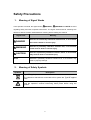
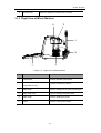
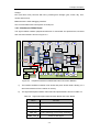
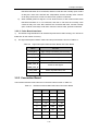
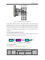
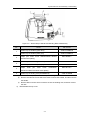
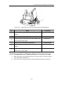
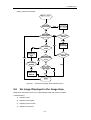
1
DP-4900/DP-6900/SK-40
Digital Ultrasonic Diagnostic Imaging System
Service Manual
Revision 6.0
Version information
Ver.
System Date
Revision description
1.0
2007.9
Initial version
2.0
2009.5
Modify Keyboard PCBA theory
3.0
2009.10
Increase new electric safety test
4.0
2010.7
Use new LOGO
5.0
2011.7
Add new model type
6.0
2012.9
Update the test items, test methods and limits of
electrical safety inspection.
Affected page list
Page range
Content
Ver.
A-8,A-11,A-14,A-16
The limits of test items
6.0
A-1-1
Electrical Safety Inspection Form.
6.0
Content
Content ................................................................................................................................... i
Intellectual Property Statement ............................................................................................. I
Responsibility on the Manufacturer Party ............................................................................ II
Warranty ............................................................................................................................... II
Exemptions ........................................................................................................................... II
Return Policy ....................................................................................................................... IV
Company Contact ................................................................................................................ IV
Safety Precautions ............................................................................................................... V
1
2
System Introduction ............................................................................. 1-1
1.1
Intended Use .......................................................................................................... 1-1
1.2
Contraindication ..................................................................................................... 1-1
1.3
Product and Model Code........................................................................................ 1-1
System Structure .................................................................................. 2-1
2.1
Introduction of Each Unit ........................................................................................ 2-1
2.1.1 Appearance of the System ................................................................................... 2-1
2.1.2 Front View of Whole Machine............................................................................... 2-2
2.1.3 Right View of Whole Machine............................................................................... 2-3
2.1.4 Left View of Whole Machine ................................................................................. 2-4
2.1.5 Back View of Whole Machine ............................................................................... 2-4
3
2.2
Introduction of Control Panel .................................................................................. 2-5
2.3
Introduction of Rear I/O .......................................................................................... 2-7
Principle Description ............................................................................ 3-1
3.1
Schematic Diagram of the System ......................................................................... 3-1
3.2
Principle of Boards ................................................................................................. 3-2
3.2.1 Main Board ........................................................................................................... 3-2
3.2.2 Probe Board........................................................................................................ 3-10
3.2.3 Connection Board ............................................................................................... 3-12
3.2.4 IO Board ............................................................................................................. 3-14
3.2.5 Control Panel Module ......................................................................................... 3-16
3.2.6 Power Supply Board ........................................................................................... 3-21
4
System Structure and Assembly / Disassembly ................................ 4-1
4.1
Exploded View ........................................................................................................ 4-1
4.1.1 Overall Exploded View ......................................................................................... 4-1
i
4.1.2 Exploded View of Keyboard Module .................................................................... 4-3
4.1.3 Exploded View of Main Unit Box Module ............................................................. 4-5
4.2
Structure Disassembly............................................................................................ 4-6
4.2.1 Disassemble Top Cover ........................................................................................ 4-6
4.2.2 Disassemble IO Back Cover................................................................................. 4-8
4.2.3 Disassemble and Replace IO Board .................................................................. 4-10
4.2.4 Disassemble Back Cover of Main Unit Box ........................................................ 4-11
4.2.5 Disassemble and Replace Power supply board ................................................. 4-12
4.2.6 Disassemble and Replace Main Board and Probe Board .................................. 4-13
4.2.7 Disassemble and Replace Harddisk(Optional devices) ................................ 4-17
4.2.8 Disassemble and Replace CRT, CRT Adjustment Board and Main Unit
Connection Board ........................................................................................................ 4-19
4.2.9 Disassemble and Replace Monitor Protection Screen ....................................... 4-21
4.2.10 Disassemble Keyboard, Trackball and Speaker ............................................... 4-22
4.2.11 Disassemble and Replace Fan and Dustproof Net .......................................... 4-26
4.2.12 Disassemble USB Extension Line .................................................................... 4-27
4.3
Installation of Optional Devices ............................................................................ 4-28
4.3.1 Installation of Video Printer ................................................................................. 4-28
4.3.2 AC Mobile Power DA-88 ..................................................................................... 4-29
4.3.3 Footswitch........................................................................................................... 4-29
5
Maintenance Requirements ................................................................. 5-1
5.1
Tools Used in Maintenance .................................................................................... 5-1
5.1.1 Tools, Measurement Devices, Consumables ....................................................... 5-1
5.2
6
Maintenance Personnel.......................................................................................... 5-2
Checking ................................................................................................ 6-1
6.1
System Status Checking ........................................................................................ 6-1
6.1.1 Checking Plan ...................................................................................................... 6-1
6.1.2 Confirmation before Checking .............................................................................. 6-1
6.2
Checking Functionality ........................................................................................... 6-2
6.2.1 Flow of Functionality Checking ............................................................................. 6-2
6.2.2 Details of Functionality Check .............................................................................. 6-2
6.3
Safety Checking ..................................................................................................... 6-3
6.3.1 Mechanical Safety Checking ................................................................................ 6-3
6.3.2 Electrical Safety Checking .................................................................................... 6-5
6.4
Image Checking ..................................................................................................... 6-5
ii
6.4.1 Image Recording and Archiving............................................................................ 6-5
6.4.2 Checking Flow ...................................................................................................... 6-5
6.4.3 Checking Phantom Data ....................................................................................... 6-6
6.4.4 Final Operation Checking and Image Archiving ................................................... 6-6
7
System Maintenance ............................................................................ 7-1
7.1
System Cleaning .................................................................................................... 7-1
7.1.1 Cleaning Flow ....................................................................................................... 7-1
7.1.2 Details for Cleaning .............................................................................................. 7-1
7.2
Software Maintenance ............................................................................................ 7-4
7.2.1 Preset ................................................................................................................... 7-4
7.2.2 Viewing System Information ................................................................................. 7-4
7.2.3 Data Backup and Recovery .................................................................................. 7-5
7.2.4 Maintenance Status .............................................................................................. 7-6
7.2.5 Software Updating ................................................................................................ 7-7
7.2.6 Installing and Uninstalling the Software of Optional Devices ............................... 7-8
7.2.7 System Self test .................................................................................................... 7-9
8
Troubleshooting .................................................................................... 8-1
8.1
USB can’t be Recognized ...................................................................................... 8-1
8.2
Abnormal System Clock ......................................................................................... 8-1
8.3
System Power, Fan Speed Check .......................................................................... 8-1
8.4
The System can’t be Started .................................................................................. 8-1
8.5
Blank Screen .......................................................................................................... 8-1
8.6
No Image Displayed in the Image Area .................................................................. 8-2
8.7
Snow in Image ........................................................................................................ 8-3
8.8
Application of Self test ............................................................................................ 8-3
8.8.1 Checking Voltage for Each Channel ..................................................................... 8-3
8.8.2 Checking Electrical Quantity of Real-time Clock Battery ..................................... 8-4
8.8.3 Checking Fan Status ............................................................................................ 8-4
8.8.4 Checking Peripheral Devices Interfaces .............................................................. 8-4
8.8.5 Checking Correctness of Front End Control......................................................... 8-4
8.8.6 Checking Probe Board ......................................................................................... 8-4
8.8.7 Checking Keyboard Board.................................................................................... 8-4
8.9
Probe Board Malfunction ........................................................................................ 8-5
8.9.1 Single Socket Probe Board can’t be Recognized ................................................ 8-5
8.9.2 Double Sockets Probe Board an’t be Recognized ............................................... 8-5
iii
8.10
Malfunction of Control Panel .................................................................................. 8-5
8.11
Troubleshooting of Power Supply Board ................................................................ 8-6
Appendix A Electrical Safety Inspection .................................................. A-1
iv
© 2009-2012 Shenzhen Mindray Bio-medical Electronics Co., Ltd. All Rights Reserved.
For this Service Manual, the issued Date is 2012-09.
Intellectual Property Statement
SHENZHEN MINDRAY BIO-MEDICAL ELECTRONICS CO., LTD. (hereinafter called Mindray)
owns the intellectual property rights to this Mindray product and this manual. This manual may
refer to information protected by copyrights or patents and does not convey any license under
the patent rights of Mindray, nor the rights of others. Mindray does not assume any liability
arising out of any infringements of patents or other rights of third parties.
Mindray intends to maintain the contents of this manual as confidential information. Disclosure
of the information in this manual in any manner without the written permission of Mindray is
strictly forbidden.
Release, amendment, reproduction, distribution, rental, adaptation or translation of this
manual, in any manner whatsoever without the written permission of Mindray, is strictly
forbidden.
,
,
,
,
,
are the registered trademarks or
trademarks owned by Mindray in China and other countries.
All other trademarks that appear
in this manual are used only for editorial purposes without the intention of improperly using
them. They are the property of their respective owners.
I
Responsibility on the Manufacturer Party
Contents of this manual are subject to changes without prior notice.
All information contained in this manual is believed to be correct. Mindray shall not be liable for
errors contained herein nor for incidental or consequential damages in connection with the
furnishing, performance, or use of this manual.
Mindray is responsible for the effects on safety, reliability and performance of this product, only
if:
All installation operations, expansions, changes, modifications and repairs of this product
are conducted by Mindray authorized personnel;
The electrical installation of the relevant room complies with the applicable national and
local requirements;
The product is used in accordance with the instructions for use.
Upon request, Mindray may provide, with compensation, necessary circuit diagrams,
calibration illustration list and other information to help qualified technician to maintain and
repair some parts, which Mindray may define as user serviceable.
Note
This equipment is not intended for family usage.
This equipment must be operated by skilled/trained medical professionals.
Warning
It is important for the hospital or organization that employs this equipment to carry out a
reasonable service/maintenance plan. Neglect of this may result in machine breakdown or
injury of human health.
Warranty
THIS WARRANTY IS EXCLUSIVE AND IS IN LIEU OF ALL OTHER WARRANTIES,
EXPRESSED OR IMPLIED, INCLUDING WARRANTIES OF MERCHANTABILITY OR
FITNESS FOR ANY PARTICULAR PURPOSE.
Exemptions
Mindray's obligation or liability under this warranty does not include any transportation or other
charges or liability for direct, indirect or consequential damages or delay resulting from the
II
improper use or application of the product or the use of parts or accessories not approved by
Mindray or repairs by people other than Mindray authorized personnel.
This warranty shall not extend to:
Any Mindray product which has been subjected to misuse, negligence or accident;
Any Mindray product from which Mindray's original serial number tag or product
identification markings have been altered or removed;
Any product of any other manufacturer.
Safety, Reliability and Performance
Mindray is not responsible for the effects on safety, reliability and performance of the product if:
Assembly operations, extensions, re-adjusts, modifications or repairs are carried out by
persons other than those authorized by Mindray.
Personnel unauthorized by Mindray repairs or modifies the instrument.
III
Return Policy
Return Procedure
In the event that it becomes necessary to return this product or part of this product to Mindray,
the following procedure should be followed:
1.
Obtain return authorization: Contact the Mindray Service Department and obtain a
Customer Service Authorization (Mindray) number. The Mindray number must appear on
the outside of the shipping container. Returned shipments will not be accepted if the
Mindray number is not clearly visible. Please provide the model number, serial number,
and a brief description of the reason for return.
2.
Freight policy: The customer is responsible for freight charges when this product is
shipped to Mindray for service (this includes customs charges).
3.
Return address: Please send the part(s) or equipment to the address offered by Customer
Service department
Company Contact
Manufacturer:
Shenzhen Mindray Bio-medical Electronics Co., Ltd.
Address:
Mindray Building, Keji 12th Road South, Hi-tech Industrial Park,
Nanshan, Shenzhen 518057, P. R. China
Phone:
+86 755 26582479 26582888
Fax:
+86 755 26582934 26582500
IV
Safety Precautions
1.
Meaning of Signal Words
In this operator’s manual, the signal words
DANGER,
WARNING and NOTE are used
regarding safety and other important instructions. The signal words and their meanings are
defined as follows. Please understand their meaning before reading this manual.
Signal word
DANGER
WARNING
CAUTION
Meaning
Indicates an imminently hazardous situation that, if not avoided,
will result in death or serious injury.
Indicates a potentially hazardous situation that, if not avoided,
could result in death or serious injury.
Indicates a potentially hazardous situation which, if not avoided,
may result in minor or moderate injury.
Indicates a potentially hazardous situation that, if not avoided, may
NOTE
result in property damage.
2.
Meaning of Safety Symbols
Symbols
Description
Type-BF applied part
The ultrasound transducers connected to this system are Type-BF applied
parts.
"Attention" indicates the points that you should pay attention to. Be sure to
read the operator’s manual concerning these points before using the
system.
V
3.
Safety Precautions
Please observe the following precautions to ensure patient’s and operator’s safety when using
this power.
DANGER:
Do not use flammable gasses, such as anesthetic gas, oxygen
or hydrogen, or flammable liquids such as ethanol, near this
power, because there is danger of explosion.
WARNING:
1.
2.
3.
4.
5.
6.
Do not charge the device within PATIENT ENVIRONMENT.
When the DC input cable is connected to the DC output (cigar lighter of a vehicle)
or the mobile power, do not touch the patient and the metal part of the DC input
cable simultaneously.
After charging through the cigar lighter of a vehicle, the connector of the DC input
cable may get hot. Do not touch the metal part of the connector to avoid scald.
Electric shock hazard! Refer all servicing to qualified service personnel only.
Do not place the device in locations near fire, high temperature, inflammable and
explosive material and locations exposed to direct sunlight.
The mobile power is an internally powered device, which
1) will warn when battery low (L2 yellow, dual buzzes every 30 seconds) and stop
AC output automatically when battery exhausted; and
2) may activate self-protection and stop AC output when environment
temperature is high, which will shorten the service time;
so be careful when using the device as a power supply.
7.
Do not immerse the device into water. Do not try to put out a fire with water. Do not
block the ventilation slots.
VI
NOTE:
1.
After using the device or when the device stops AC output automatically due to exhausted
battery, please switch off the AC OUT to avoid over discharging. Charge the device
immediately if possible to avoid performance degrading or even permanently damage.
2.
If the device is not used for a long time, put the device in locations shady and cool with the
battery full of power and the switch of AC output off. Maintain the device by charging
periodically (about every 3 months).
3.
Do not connect the device to AC/DC input when using the mobile power as a power
supply, or the device will stop the AC output which may cause data lost.
4.
Do not plug in AC INPUT and DC INPUT cables simultaneously.
5.
This device is for Mindray portable black-and-white ultrasonic system only. Do not
connect devices other than those specified.
6.
7.
8.
Keep the device horizontal to avoid falling.
Do not remove protective covers. No user serviceable parts are inside.
Electrical and mechanical performance may be degraded due to long usage (such as
current leakage or distortion and abrasion). To ensure the performances of this device,
please perform periodical checks for the device.
9.
To dispose of the system or any part, contact Mindray Customer Service Department or
sales representative. Mindray is not responsible for any system content or accessories
that have been discarded improperly.
4.
Warning Labels
The warning labels are attached to this system in order to call your attention to potential
hazards.
The symbol
on the warning labels indicates safety precautions. The warning labels use
the same signal words as those used in the service manual.
Refer to the service manual for detailed information about the warning labels. Read operator’s
manual carefully before using the system.
5.
Symbol Explanation
VII
Symbol
Meaning
Position
Mian unit power is off
│
Power switch
Main unit power is on
Video print control interface
Video output
VGA output
On
the
input
/output panel
Interface of footswitch
USB interface
Network interface
Probe socket A
A
Probe socke
Probe socke B
B
VIII
System Introduction
1
1.1
System Introduction
Intended Use
The DP-6900 is universal B-mode digital diagnostic ultrasound system intended for use in
ultrasound exams for human.
The DP-4900/SK-40 is arised from DP-6900 by simplifying some functions and reducing some
performances, which is also intended for use in ultrasound exams for human.
The DP-6900Vet modified from DP-6900 is B-mode digital diagnostic ultrasound system,
which is intended for use in ultrasound exams for animals.
The DP-4900Vet modified from DP-4900 is digital diagnostic ultrasound system, which is
intended for use in ultrasound exams for animals.
1.2
Contraindication
None.
1.3
Product and Model Code
DP Model code
Product code
1-1
System Structure
2
2.1
System Structure
Introduction of Each Unit
2.1.1 Appearance of the System
Figure 2-1
Appearance (1)
Figure 2-2
Appearance (2)
2-1
System Structure
No
Name
Function
1
Control panel
Operator-system interface or control
2
Monitor
Displays the images and parameters during scanning
3
Handle
Used for carrying the system
4
Gel bottle holder
Used for holding the gel bottle provisionally
5
Probe holder
Used for holding the probe provisionally
6
Probe cable hook
Used for hanging the probe cable
7
Probe socket
Used for connecting a probe
8
I/O panel
Interface panel for input and output signal
9
Cable holder
Used for winding the IO cable provisionally
10
USB port
Used for connecting a USB device
2.1.2 Front View of Whole Machine
Figure 2-3
No
Front View of Whole Machine
Name
Function
1
Monitor
Displays the images and parameters etc
2
Brightness knob
Rotate it to adjust the brightness of the monitor
2-2
System Structure
3
Contrast knob
Rotate it to adjust the contrast of the monitor
2.1.3 Right View of Whole Machine
Figure 2-4
No
Right View of Whole Machine
Name
1
Control panel
2
Probe
socket
Function
Used for operating the system
(the
standard
Used for connecting a probe
configuration is one)
3
Cable holder
Used for winding the IO cable provisionally
4
Probe cable hook
Used for hanging the probe cable
5
Probe holder
Used for holding the probe
6
Handle
Used for carrying the system
2-3
System Structure
2.1.4 Left View of Whole Machine
Figure 2-5
No
Left View of Whole Machine
Name
Function
1
USB port
Used for connecting a USB device
2
Gel bottle holder
Used for holding the gel bottle
2.1.5 Back View of Whole Machine
Figure 2-6
Back View of Whole Machine
2-4
System Structure
No
Name
Function
1
IO interface
Input and output interface
2
Air vent
Air outlet of the system
2.2
Introduction of Control Panel
<2>
<3>
<4>
<5>
<6>
<7>
<8>
<9>
<10>
<1>
<11>
<12>
<13>
<16>
<14>
<15>
<22>
<21>
<17>
<
<2
>
20
<25>
<18>
4>
<2
<19>
<2
6>
<34>
<33>
<27>
<28>
<29>
<30>
<31>
<32>
3>
<36>
<37>
<35>
<38>
<39>
Figure 2-7
No.
1
Control Panel
Name
Function
Adjusts the acoustic power when rotated. The function when
A.Power
pressed can be preset
2
End Exam
Ends the current exam
3
Info
Opens/closes the patient information dialog box
4
Exam
Opens the exam mode menu to select an exam mode
5
Probe
Switches probes
6
F5
User-defined key, the function of which can be preset
7
File
Opens iStation
8
Setup
Opens the preset menu
2-5
System Structure
No.
Name
Function
9
Indicator
Reserved
10
TGC
Time Gain Compensation
11
Character & number
Used for inputting characters and symbols
keys
12
F4
User-defined key, the function of which can be preset
13
F3
User-defined key, the function of which can be preset
14
Comment
Enters/exits character comment mode
15
Arrow
Enters/exits arrow comment mode
16
F1
User-defined key, the function of which can be preset
17
F2
User-defined key, the function of which can be preset
18
Exit
Exits a dialog box without saving changes
19
Cine
Switches
between
auto/manual
cine
review
modes.
Releases the cursor
20
Measure
Enters/exits measure mode
21
Body Mark
Adds body mark to the image
22
Clear
Clears the screen
23
Menu
Opens/closes the menu of current mode
24
Set
Selects items/Confirms an operation/Increases a parameter
25
Change
Switches among items before beginning a measurement;
Switches between cursors during a measurement
26
Cancels the last step when measuring/Decreases a
Back
parameter
27
Switches to dual B mode. Or
Dual
Switches between windows in dual B mode
28
Switches to quad B mode. Or
Quad
Switches among windows in quad B mode
29
V.Rev.
Flips the image vertically
30
B
Switches to B mode
31
M
Switches to M+B or M mode
32
H.Rev.
Flips the image horizontally
2-6
System Structure
No.
Name
Function
Press to switch among items and rotate to adjust the
33
Multifunctional Knob
(L): F.Pos./Freq./IP
corresponding item:
F.Pos.: Adjusts location of the focus
Freq.: Switches the transmitting frequency
IP: Adjusts the image quality according to a set of
preset image parameters
34
Save
Saves an image as preset format
35
Track Ball
Moves the cursor
36
Gain
Adjusts the gain of image when rotated. The function when
pressed can be preset
Press to switch among items and rotate to adjust the
Multifunctional
37
(R):
knob
Depth/Zoom/
Rotation
corresponding item:
Depth: Adjusts the depth
Zoom: Magnifies the image
Rotation: Rotates the arrow mark or the probe
mark of the body mark
38
Print
Printing
39
Freeze
Freezes/unfreezes the image
2.3
Introduction of Rear I/O
Figure 2-8
No.
1
Rear I/O Ports
Symbol
Function
Connects the remote cable of the video printer
2-7
System Structure
2
Connects to the video input port of the video printer
3
Accepts the network cable
4
Connects to the video input port of the video printer
5
Connects an external monitor
6
AC IN
Accepts the power cord
7
Power switch
Power on/off
8
Accepts a foot switch
2-8
Principle Description
3
3.1
Principle Description
Schematic Diagram of the System
Transmitting/receiving of main board
80ch
Probe
interface
Control
80ch
Low-voltage
transmitting
drive
High-voltage
transmitting
drive
Probe
selection
Probe
structure
Signal
processing
and control
module
80ch
PHV
Probe board
Transmitting/
receiving
switch
+5V
Control panel
TGC
RAM
For
DSC
Control
FPGA
Control
Control
DAC
Operational 16/8ch
amplifier
PHV
Trackball
Control
ATGC
16/8ch
RAM
For
BF
Control
Rear of the
main board
ADC
PHV
control
Keyboard
Communication
interface
Encoder
SDRAM
Power module
+5V
Hard disk
AC/DC
Low-voltage
power
Central control
system
SSD
CPU bus
MCF5307
Power
13.5V
CRT
FLASH
Voltage
monitor
VGA
AC
Peripheral
interfaces
AC IN
VGA
Video
S-Video
Video
printer
control
Foot
switch
USB
Network
Fig
ure 3-1
Schematic Diagram of Hardware System Structure
The above block diagram includes probe board, main board, control panel, power module, IO
board and CRT etc.
Two modules of main board: transmitting/receiving and rear of the main board
comprise the key of the system. The control and processing centrum is central
control system and signal processing and control module. Each function module is
controlled by one of the modules or both of them.
Power module implements the switching between AC and DC providing power for
3-1
Principle Description
each part of the system. For example, the monitor only needs the power of 13.5 V.
Control panel (or called keyboard) provides operator-system interface.
Probe board provides the socket for the probe.
The system provides abundant interfaces: VGA, Video, S-Video, USB, network and
footswitch etc.
3.2
Principle of Boards
3.2.1 Main Board
3.2.1.1 Ultrasound Transmission
The front-end circuit includes four parts according to the function: low-voltage drive and
high-voltage transmitting, high-voltage isolation and channel selection, ATGC signal
amplification and AD acquisition as shown in Figure3-2 below:
Figure 3-2
Schematic Diagram of Front-end Circuit
Transmission circuit includes two parts: transmission sequence and transmission drive.
Transmission sequence generates low-voltage transmitting pulse driven by transmission, and
then it turns to high-voltage transmitting pulse to drive 80 elements.
The test points related to transmission are shown in Table 3-1.
3-2
Principle Description
Table 3-1
Test Points Related to Transmission
No.
Test points label
Description
1
TP23
Programmable high-voltage
2
TP28
12V
3.2.1.2 Ultrasound Reception
Ultrasound reception includes three parts: high-voltage isolation and reception channel
selection, voltage controlled gain amplifier and ADC. Receiving channel selection is completed
by ten SPST (single-pole single-throw) cascaded. The output of DAC is analog voltage signal,
it controls the amplification.
3.2.1.3 CPU and Peripharial Circuit
Structure of CPU is shown in Figure 3-3.
Figure 3-3
Structure of Central Control System
There are SDRAM, FLASH and FPGA on CPU bus, among which, FLASH is used for storage
of system software and key data, SDRAM is used for storage of software memory and cine
review, FPGA is controlled by CPU and communicates with CPU to implement the control of
functional circuit. In addition, FPGA implements the interface with IDE bus and the operation of
system to SSD and disc. SSD with 512MB memory capacity saves key data and remains
space for user to save general data. HD with 80G is optional part; it is used for image and cine
3-3
Principle Description
storage.
RTC (real time clock) connects with CPU, providing time storage (year, month, day, hour,
minute and second).
BDM interface is CPU debugging interface.
CPU communicates with control panel via serial port.
3.2.1.4 Interfaces of Main Board
The signal relation between peripheral interfaces of main board and probe board, IO board
and connection board is shown in Figure 3-4
Figure 3-4
1)
Peripheral Interfaces of Main Board and Connection Relation
The interface definition between main board and probe board needn’t testing, so it
will not be listed here for the reason of secrecy.
2)
The signal description between main board and probe board is shown in Table 3-2.
Table 3-2
Signal Description between Main Board and Probe Board
Name
Function
POUT[80:1]
High-voltage transmitting and receiving
PRB_ID[5:0]
Probe identifies ID code/ID code of board
PRBID_RD[1:0]
Probe ID reading enable
PRB_SW
Probe switching (control relay switching)
PRBA_PRT_N
Probe on-site signal
3-4
Principle Description
PRBB_PRT_N
3)
VCC_PRB
Power of probe board, +5V
GND
Ground return
The interface definition between main board and connection board is shown in Table
3-3.
Table 3-3
Interface Definition between Main Board and Connection Board
Pin No.
A
B
C
1
PHV
PHV
PHV
2
NC
NC
NC
3
GND
GND
GND
4
-5V
-5V
-5V
5
GND
GND
GND
6
12V
12V
12V
7
GND
GND
GND
8
A+5V
A+5V
A+5V
9
A+5V
A+5V
A+5V
10
A+5V
A+5V
A+5V
11
GND
GND
GND
12
HVC
GND
GND
13
GND
GND
GND
14
GND
GND
GND
15
2V5
2V5
2V5
16
GND
GND
GND
17
1V5
1V5
1V5
18
1V5
1V5
1V5
19
GND
GND
GND
20
GND
GND
GND
21
3V3
3V3
3V3
22
3V3
3V3
3V3
23
GND
GND
GND
24
GND
GND
GND
25
13V5
13V5
13V5
26
VS
GND
GND
27
HS
GND
B
3-5
Principle Description
4)
A
B
C
28
GND
GND
GND
29
TXD
GND
RXD
30
GND
GND
GND
31
D+5V
D+5V
D+5V
32
D+5V
D+5V
D+5V
The interface definition between main board and IO board is shown in Table 3-3.
Table 3-3
Interface Definition between Main Board and IO Board
Pin No.
5)
Pin No.
Name
Pin No.
Name
1
VIDEO
2
GND
3
Blue_OUT_R
4
Blue_OUT_G
5
Blue_OUT_B
6
GND
7
GND
8
F_VGA_HSYNC
9
FT_SW1
10
F_VGA_VSYNC
11
FT_SW0
12
GND
13
GND
14
S_VIDEO
15
VP_BUSY
16
CI
17
VP_NPRT
18
CT7
19
GND
20
GND
21
TPIP
22
TPOP
23
TPIN
24
TPON
25
GND
26
GND
27
FAN_PWR
28
FAN_SPEED1
29
FAN_SPEED2
30
FAN_SPEED3
The signal description between main board and IO board is shown in Table 3-4.
Table 3-4 Signal Description between Main Board and IO Board
Module
Video output
Network port
Name
Description
VIDEO
Video output
S_VIDEO
S_Video output
TPOP
Output data
TPON
Output data
TPIP
Input data
TPIN
Input data
Difference pair
Difference pair
3-6
Principle Description
CT7
VGA
BLUE_R
Video output
BLUE_G
Tap
VGA signal output
BLUE_B
HSYNC
Horizontal hold
VSYNC
Field locking
Remote
REMOTE
Video printer control
Footswitch
FT_SW0
FT_SW1
Video printer
Fan
Uncovering Inspection
VP_NPRT
Print
VP_BUSY
Printer is busy
FAN_PWR
Fan power
FAN_SPEED1
Fan monitoring
FAN_SPEED2
Fan monitoring
FAN_SPEED3
Fan monitoring
CI
3.2.1.5 Main Board Power
Main board power is connected with power supply board by connection board. All powers are
processed LC filtering at the sockets of main board entrance firstly and then assingned to the
devices within the board. There is fuse on main board end. The structure of main board power
is shown in Figure 3-5.
Fuse F3: M07-00077F - (FUSE Slow-Blow 125V 5ASMD2410).
Fuse F1-2 and F4-9: M07-00076F - (FUSE protective tube Slow-Blow125V 3ASMD2410).
3-7
Principle Description
Figure 3-5
Sketch Map of Main Board Power
3.2.1.6 System Monitoring
3.2.1.6.1. Voltage Monitoring
Voltage monitoring circuit mainly monitors +1.2V, +2.5V, +3V, +3.3V, +5V, +12V, +
13.5V, -1.5V, -5V and PHV (Programmable high-voltage) of the system, among which,
except +5V, +12V, +3.3V, +2.5V and +1.2V, other voltages are all monitored by dividing
voltage or inverting conversion. In addition to monitoring each channel voltage and internal
voltage entering by connection board, IDT7462 also inspects the voltage of 3V lithium battery.
Voltage monitoring is implemented by ADT7462, completely compatible with SMBus1.1 and
SMBus1.0 protocols.
3.2.1.6.2. Monitoring of Fan Blockage
The fan signals used by the machine belong to R Type, in which, the third channel signal is
running sensor or blockage signal.
When the fan is running, blockage signal is low (0V); when the fan is blocked, the signal is high
(3.3V).
When the fan is wrongly connected, the signal is also high.
3.2.1.7 Test Points of Main Board
Test Points of main board is shown in Table 3-5:
Table 3-5
No.
1
Test Points of Main Board
Label
1V2
Network
1V2
3-8
Principle Description
No.
Label
Network
2
1V5
1V5
3
2V5
2V5
4
A+3
A+3
5
A+5
A+5
6
A1V8
A1V8
7
A3V3
A3V3
8
AVCC
AVCC
9
AVDD
AVDD
10
AVPP
AVPP
11
CLK45M
FPGA_CLK45_NORM
12
CLK_CPU
CPU_CLK_I
13
FPGA_RST
FPGA_RSTI
14
GND
GND
15
M13V5
13V5
16
NA1V5
NA1V5
17
NA5V
NA5V
18
PHV
PHV
19
RST_CPU
CPU_RSTI_N
20
SCL
SCL
21
SDA
SDA
22
POUT41
POUT41
23
TP1
IDE_DMAREQ
24
TP2
IDE_DMACK_N
25
TP5
SPI_5625_CLK
26
TP8
IO_RESET_N
27
TPU71
TPU71
28
TP10
IO_DQS3R_CDPCLK4
29
TP11
UAI
30
TP12
UAO
31
TP13
IDE2SATA_CLK
32
TP14
SCIDIN
33
TP15
SCICLK
34
TP16
IO_DIFFIO_DQS1R_DPCLK6
3-9
Principle Description
No.
Label
Network
35
TP17
SCIDOUT
36
TP18
SPI_5626_DIN
37
TP19
SPI_5626_CS
38
TP20
SPI_714_CS
39
TP21
SPI_714_CLK
40
TP22
CPU_ADDR0
41
TP24
VDD
42
TP27
GND
43
TPU75
TPU75
44
TPU79
TPU79
45
VCC
VCC
3.2.2 Probe Board
3.2.2.1 Principle of Probe Board
Standard configuration of the product is single socket probe board, but double sockets probe
board is optional.
Double sockets probe board mainly includes A, B probe sockets, 80-channel selection circuit,
probe and PCB-ID output circuit, relay control circuit and power circuit. Single socket probe
board mainly includes probe socket, probe and PCB-ID output circuit and power circuit.
3-10
Principle Description
Figure 3-6
Figure 3-7
Figure 3-8
Schematic Diagram of Double Sockets Probe Board
Schematic Diagram of Single Socket Probe Board
Double Sockets Probe Board Relay Drive Circuit
Control circuit connection of DPDT (double-pole double-throw relay) is shown in the above
figure. Control signals are RC1, RC2, RO1 and RO2, respectively controls 10 relays, totally 40
relays and 80 channels.
1)
When PROBE_SWITCH signal is in high electrical level, N slot enhancement-mode
3-11
Principle Description
field-effect transistor Q1 is conducted, and then it will drive the normally open contact
of relay K41 close. RC1 and RC2 are susupended, and the normally close contacts
of 20 relays under their control are closed. Now, probe A is selected.
2)
When PROBE_SWITCH signal is in low electrical level, N slot enhancement-mode
field-effect transistor 2 is not conducted, and then it will drive the normally close
contact of relay K41 close. RC1 and RC2 are connected with VCC, and the normally
open contacts of 20 relays under their control are closed. Now, probe B is selected.
3.2.2.2 Probe Board Interfaces
1)
The interface signal between main board and probe board needn’t testing, so it will not be
listed here for the reason of secrecy.
2)
The signal description between main board and probe board is shown in Table 3-6.
Table 3-6
Signal Description between Main Board and Probe Board
Name
Function
POUT[80:1]
High-voltage transmitting and receiving
PRB_ID[5:0]
Probe identifies ID code/ID code of board
PRBID_RD[1:0]
Probe ID reading enable
PRB_SW
Probe switching (control relay switching)
PRBA_PRT_N
Probe on-site signal
PRBB_PRT_N
VCC_PRB
Power of probe board, +5V
GND
Ground return
3.2.3 Connection Board
The interface between main board and connection board is shown in Table 3-7.
Table 3-7
Interfaces between Main Board and Connection Board
No.
A
B
C
1
PHV
PHV
PHV
2
NC
NC
NC
3
GND
GND
GND
4
-5V
-5V
-5V
5
GND
GND
GND
6
12V
12V
12V
7
GND
GND
GND
8
A+5V
A+5V
A+5V
3-12
Principle Description
No.
A
B
C
9
A+5V
A+5V
A+5V
10
A+5V
A+5V
A+5V
11
GND
GND
GND
12
HVC
GND
GND
13
GND
GND
GND
14
GND
GND
GND
15
2V5
2V5
2V5
16
GND
GND
GND
17
1V5
1V5
1V5
18
1V5
1V5
1V5
19
GND
GND
GND
20
GND
GND
GND
21
3V3
3V3
3V3
22
3V3
3V3
3V3
23
GND
GND
GND
24
GND
GND
GND
25
13V5
13V5
13V5
26
NC
GND
GND
27
NC
GND
NC
28
GND
GND
GND
29
NC
GND
NC
30
GND
GND
GND
31
D+5V
D+5V
D+5V
32
D+5V
D+5V
D+5V
The ports communication signal with 3.3 V LVTTL level between keyboard and main board is
transferred via connection board. +5V power supply of keyboard is from D+5 of connection
board. Connection board provides an 8 pin socket; the definition is shown in Table 3-8.
Table 3-8
Interface Definition of Keyboard
No.
Name
Description
1
RXD
Data input of main board ports
2
GND
Ground
3
TXD
Data output of main board ports
4
GND
Ground
3-13
Principle Description
5
GND
Ground
6
GND
Ground
7
D+5
D+5V power
8
D+5
D+5V power
The signals main board sending to monitor are transferred via connection board. +13.5V
power supply is from 13V5 of connection board. Connection board provides a 6 pin socket and
a 4 pin socket; the interface definition of monitor signals is shown in Table 3-9.
Table 3-9
Interface Definition of Monitor Signals
No.
Name
Description
1
GND
Signal ground
2
HS
Horizontal hold signal
3
GND
Signal ground
4
VS
Field locking
5
GND
Signal ground
6
B
BLUE signal
The interface definition of monitor power is shown in Table 3-10.
Table 3-10
Interface Definition of Monitor Power
No.
Name
Description
1
GND
Power ground
2
GND
Power ground
3
13V5
+13.5V power
4
13V5
+13.5V power
3.2.4 IO Board
IO board is fixed on sheet-metal. Except USB port is on the side of the device, footswitch
socket is on the sheet-metal at the back of the device; all other external IO interfaces (Video,
S-Video, VGA, Remote and network) are on IO board.
3-14
Principle Description
Main board
Cable
Fan 1 2
&3
Socket
VGA
Video
Network
transformer
Remote
S-Video
Network
Socket
for foot
switch
IO board
Figure 3-9
Sketch Map of IO Board Connection Relation
IO board is connected with main board by wires. The interface definition is shown in Table
3-11.
Table 3-11
No.
Interface Definition between Main Board and IO Board
Name
No.
Name
1
VIDEO
2
GND
3
Blue_OUT_R
4
Blue_OUT_G
5
Blue_OUT_B
6
GND
7
GND
8
F_VGA_HSYNC
9
FT_SW1
10
F_VGA_VSYNC
11
FT_SW0
12
GND
13
GND
14
S_VIDEO
15
VP_BUSY
16
CI
17
VP_NPRT
18
CT7
19
GND
20
GND
21
TPIP
22
TPOP
23
TPIN
24
TPON
25
GND
26
GND
27
FAN_PWR
28
FAN_SPEED1
29
FAN_SPEED2
30
FAN_SPEED3
The signal definition of connection socket of footswitch cable is shown in Table 3-12.
3-15
Principle Description
Table 3-12
Signal Definition of Connection Socket of Footswitch Cable
No.
Name
1
ROW
3
FT_SW0
5
FT_SW1
7
GND
3.2.5 Control Panel Module
The peripheral of control panel mainly includes encoder, thin-film switch, trackball, LED,
speaker
and
TGC
etc.
The
schematic
diagram
Figure 3-10.
3-16
of
control
panel
is
shown
in
Principle Description
Figure 3-10
Schematic Diagram of Control Panel
3.2.5.1 Description of LED Drive Circuit
Just as shown in Figure 3-11, LED includes green backlighting lights and yellow indicating
lights. It only needs backlighting lights with unicolor LED for common keys. While, function
keys adopts bicolor LED in green and yellow, which means backlighting lights and indicating
lights are both needed.
The anode of all unicolor and bicolor LEDs is the same one. LED_ROW signal output from
FPGA will go through LED drive circuit that is composed of MOS tube EL7212 and PMOS tube
IRF7404 to output LED_DRIVE signal to drive LED. For common keys, the cathode of unicolor
LED is directly grounded with 750hm current-limiting resistance. For function keys, each two
bicolor LEDs are drived by 74LS07 via two pins of FPGA to achieve the purpose that switching
between backlighting lights and indicating lights.
3-17
Principle Description
Figure 3-11
Schematic Diagram of LED Drive Circuit
3.2.5.2 Description of Key Scanning Circuit
The key matrix adopts the signal in row and line control metood. Testing signal will be output
from FPGA line by line. When press a certain key, the signal in row will be corresponding to a
signal in line. The location of the pressed key can be known from sequency number of row and
line. The schematic diagram of key scanning is shown in Figure 3-12.
3-18
Principle Description
Figure 3-12
Schematic Diagram of Key Scanning
Thin-film switch adopts the three layers implementation method of upper wiring film, lower
wiring film and middle insulation film. The middle insulation film takes the function of
separation and opens a hole at key contact. The upper and lower wiring film form two poles at
key contact. When pressing the key, the up and down poles are conducted. When the key is
unpressed, for the separation of middle insulation film, the up and down poles are
unconnected.
3.2.5.3 Description of Speaker Drive Circuit
The keyboard board adopts the project of PWM plus RC Ffilter and speaker acoustics. The
sketch map of speaker drive method is shown in Figure 3-13.
Figure 3-13
Sketch Map of Speaker Drive Method
3.2.5.4 Socket Definition
The socket definition of control pane is shown in Table 3-13.
Table 3-13
Socket
Name
Socket Definition of Control Panel
Pin definition
number
Pin
on PCB
No
Pin definition
3-19
Pin description
Remarks
Principle Description
Socket
1
+5V
5V power
2
+5V
5V power
3
GND
System ground
4
RXD_KEY_IN
Main unit serial
of
keyboard
J5
and
port signal output
connection
board
5
GND
System ground
6
TXD_KEY_OUT
Main unit serial
port signal input
1
GND
System ground
2
VCC
5V power
3
TRACK_HBALL0
Trackball
signal
interface 0
Trackball
4
TRACK_HBALL1
Trackball
signal
J3
socket
interface 1
5
TRACK_HBALL2
Trackball
signal
interface 2
6
TRACK_HBALL3
Trackball
signal
interface 3
1
NC
2
NC
FKEY_ROW:
key
scanning
signal in row
NC:
connectionless
Socket
definition of
thin-film
J2
3
FKEY_ROW13
4
NC
5
FKEY_ROW12
6
NC
7
FKEY_ROW11
8
NC
9
FKEY_ROW10
10
NC
11
FKEY_ROW9
12
NC
13
FKEY_ROW8
14
NC
15
FKEY_ROW7
16
NC
17
FKEY_ROW6
18
NC
19
FKEY_ROW5
20
NC
21
FKEY_ROW4
22
NC
23
FKEY_ROW3
24
NC
25
FKEY_ROW2
26
NC
switch
upper
wiring
3-20
Principle Description
27
FKEY_ROW1
28
NC
29
FKEY_ROW0
30
NC
1
NC
2
KEY_LINE3
KEY_LINE:
key
scanning
signal in line
NC:
connectionless
Socket
definition of
thin-film
J6
3
NC
4
KEY_LINE2
5
NC
6
KEY_LINE1
7
NC
8
KEY_LINE0
9
NC
10
KEY_LINE4
11
NC
12
KEY_LINE5
13
NC
14
KEY_LINE6
15
NC
16
KEY_LINE7
17
NC
18
NC
19
NC
20
NC
21
NC
22
NC
23
NC
24
NC
25
NC
26
NC
27
NC
28
NC
29
NC
30
NC
1
TCK
JTAG clock
2
TDO
JTAG data output
3
TMS
JTAG TMS
4
TDI
JTAG data input
5
VDD
VDD voltage
6
GND
System ground
1
BUZ0
Speaker positive
switch
lower
wiring
JTAG
J4
socket
definition
J8
Speaker
socket
end input
2
BUZ1
Speaker negative
end input
3.2.6 Power Supply Board
3.2.6.1 Overview
Power system is the power supply for whole ultrasonic diagnostic system. It mainly supplies
3-21
Principle Description
the system with +5V (D+5V and A+5V), -5V, +12V, +13.5V, +3.3V, +1.5V, +2.5V and
programmable high-voltage, totally 9 groups DC output.
The performance index of each output is shown in Table 3-14.
Table 3-14
Rating
No
.
voltage
(V)
)
Performance Index of Power Supply Board Output
Voltag
Ratin
e
g
accur
load
Ripple
Minim
al load
acy
Voltage
Load
regulatio
regulation
n rate
rate
noise
(mVpk -
Use
pk)
Analog
1
2
A+5V
3A
D+5V
3.5A
0.5A
part/keybo
1.0A
<30m
ard
V
Keyboard/
USB
3
-5.0V
0.4A
20mA
Amplifier
4
+13.5V
1.5A
0.3A
VGA
±5%
5
+12V
<2%
0.35A
Fan
<5%
100mA
<50m
/CMOS
V
drive
Transmitti
6
HV
50mA
0
ng circuit
7
+3.3V
3.5A
0.2A
Digital part
<30m
8
+2.5V
1.0A
0.2A
Digital part
V
9
+1.5V
2.0A
0.2A
Digital part
3.2.6.2 Principle
The schematic diagram of power supply board is shown in Figure 3-14.
3-22
Principle Description
EMI filter
AC &surge
current
input suppression
circuit
BOOST
APFC
Forward
transformer
circuit
Magnetic
amplification
adjustment 1
OCP&OVP
Magnetic
amplification
adjustment 2
OCP&OVP
+13.5V output
+12V output
BOOST
change
Linear
stabilizing 1
OVP&
UVP&
OTP
PHV output
OCP&OVP
Level translation
circuit
Isolating
drive
A+5V output
+5V
D+5V output
PWM
controller
Feedback OVP&
circuit
OVP
Optical
coupling
isolation
Figure 3-14
PHV control signal
DC/DC
change
-5V output
BUCK
change
+3.3V output
Linear
stabilizing 2
+2.5V output
Linear
stabilizing 3
+1.5V output
Schematic Diagram of Power Supply Board
Just as shown in the above figure, power supply board includes four parts: input part, PFC
front end, FORWARD transformer and inferior DC-AC circuit.
AC input firstly goes through EMI filter and surge current suppression circuit, and
then it is regulated by BOOST APFC for power factor, simultaneously it outputs
steady 390V DC power as the input of inferior FORWARD transformer. The
FORWARD transformer which can output +5V, -5V, +13.5V and +24V, among which,
+24V is the input of programmable high-voltage PHV, +13.5V is dropped to +12V via
two diodes, while +5V is diverted to A+5V and D+5V as the input of +3.3V, +1.5V etc.
DC-AC transformer, at last, +3.3V is regulated to +2.5V via linear stabilizing.
PFC circuit adopts UC3845 produced by TI Company as control chip, and is BOOST
transformer based on mean current mode controlling with excellent and reliable
performance. In addition, switching tube adopts IRFPC60LC produced by IR with the
parameter of 600V/16A and fly-wheel tube adopts ISL9RL1560G2 produced by
FAIRCHILD with the parameter of 600V/15A.
The controlling chip U3 of FORWARD is MB3769A produced by FUJITSU, which is a
controlling chip of voltage type. Transformer T1 also meets the requirements of
safety insulation. Switching tube adopts 2SK2485 produced by NEC with the
parameter of 900V/6A. The main feedback output of FORWARD transformer is +5V,
3-23
Principle Description
while +13.5V is exactly regulated via magnetic amplifier, -5V output is regulated via
LM337 linear stabilizing.
HV output is obtained by BOOST transformer. Controlling chip is TL594 produced by
ON-SEMI, which is a controlling chip of voltage type. HV output voltage is controlled
by 0~4V analog signals and changed linearly corresponding to the change of
controlling signals.
+3.3V and +1.5V output adopots BUCK variator based on synchronous rectification with high
efficiency and reliability. Controller adopots EL7566 produced by INTERSIL, which is a device
integrating controlling chip and on-off device as a whole. +3.3V output is turned to +2.5V after
linear stabilizing, which is implemented by discrete devices with the merit of low voltage
difference.
The power supply board has the following protection functions: PFC output overvoltage
protection, overtemprature protection, +5V output overvoltage/overcurrent/short circuit
protection, +13.5V output overvoltage/overcurrent/short circuit protection, HV output
overvoltage /overcurrent /short circuit protection, and short circuit protection function of all
other output groups. The responses of the board after each protection taking effect are as
follows:
1.
When PFC output overvoltage protection, overtemprature protection or +5V output
overvoltage/overcurrent/short circuit protection take effect, the power supply board
will stop all output and maintain locking. Only when AC input is off and the
malfunction is corrected, the board can normally work after its restarting.
2.
When +13.5V output overvoltage/overcurrent/short circuit protection takes effect,
+13.5V and HV will stop output and maintain locking. After the malfunction is
corrected and all loads of +13.5V output are disconnected, the board can output
normally.
3.
When +3.3V short circuit protection takes effect, +3.3V and HV will stop output. After
the malfunction is corrected, the output can be recovered automatically.
4.
When HV output overvoltage /overcurrent /short circuit protection, -5V overcurrent
/short circuit protection, +1.5V short circuit protection or +2.5V overcurrent /short
circuit protection take effect, each group will stop its output and won’t affect other
output. Except HV maintains locking, other groups will be recovered after the
malfunction is corrected.
3-24
System Structure and Assembly / Disassembly
4
System
Structure
Assembly / Disassembly
4.1
Exploded View
4.1.1 Overall Exploded View
Figure 4-1
Overall Exploded View
4-1
and
System Structure and Assembly / Disassembly
No.
Name
PN number
Main unit box module (one probe)
2303-30-89069
Main unit box module (two probes)
2303-30-89068
Main unit box module (one probe)
2304-30-89227
Main unit box module (two probes)
2304-30-89217
Bottom cover
2303-30-89063
Bottom cover
2304-30-89218
3
IO module
2304-30-89219
4
Winding rack (die MR29064)
2300-20-29083
1
2
Rubber
cap
of
winding
rack
(die
0026-30-89585
5
MR29076)
6
Right wind guard
2300-20-29113
7
Left wind guard
2304-20-89266
8
Hook seat
2300-20-29085
9
Probe cable hook
2102-30-16949
10
Top cover (die MR29079)
11
Probe holder (die MR29082)
2300-20-29079-51
2300-20-29082
Rubber cap of handle B (pearl blue)
2300-20-29090-52
Rubber cap of handle B (dark gray)
2300-20-29090-51
4900 handle (die MR29081)
2300-20-29081-53
6900 handle (die MR29081)
2300-20-29081-54
SK-40 handle (die MR29081)
043-002045-00
12
13
Rubber cap of handle A (pearl blue)
2300-20-29089-52
Rubber cap of handle A (dark gray)
2300-20-29089-51
14
15
CRT assembly
2300-20-29149
Fixing buckle of protection screen (die
9901-20-23950
16
BS2001138)
Protection screen of monitor (4900)
2302-20-34425
10" protection screen of monitor (6900)
2107-20-46070
Silicon rubber cap of keyboard (die
2300-20-29076
17
18
MR29076)
Top cover keyboard assembly
2303-30-89065
Top cover keyboard assembly
2304-30-89221
Bottom cover keyboard assembly
2303-30-89064
19
20
4-2
System Structure and Assembly / Disassembly
Bottom cover keyboard assembly
2304-30-89220
Front cover module
2303-30-89062
Front cover module
2304-30-89228
21
4.1.2 Exploded View of Keyboard Module
4.1.2.1 Exploded View of Top Cover Keyboard Assembly
Figure 4-2
No.
Exploded View of Top cover Keyboard Assembly
Name
PN number
1
1" trackball (TP1W0)
0025-30-36802
2
Control panel PCBA
051-000183-00
3
Thin-film switch
2304-20-89283
DP-4900 silicon rubber key
049-000041-00
DP-6900 silicon rubber key
049-000040-00
4
Transparent
lamp
shade
A
(die
5
MR29069)
4-3
2300-20-29069
System Structure and Assembly / Disassembly
DP-6900 keyboard top cover
2304-20-89237-51
SK-40 keyboard top cover
C-043-002035-00
6
7
Keyboard knob C (die MR29071)
2300-20-29073
8
Keyboard knob A(die MR29071)
2300-20-29071
9
Keyboard knob B(die MR29071)
2300-20-29072
10
Keyboard toggle switch (die MR29074)
2300-20-29074
11
Transparent lamp shade B(die MR29069)
2300-20-29070
12
SPEAKER 8 ohm 15% 1.0W SPL 86
M90-100123---
4.1.2.2 Exploded View of Bottom cover keyboard assembly
Figure 4-3
Exploded View of Bottom Cover Keyboard Assembly
No.
Name
PN number
1
Bottom cover of keyboard (die MR29062)
2300-20-29062
2
DP-4900 decorative cover
2300-20-29063-56
DP-6900 decorative cover
2300-20-29063-57
SK-40 decorative cover
C-043-002034-00
3
Setting bolt spring
2300-20-29065
4
Key buckle (die MR29064)
2300-20-29064
5
Spacing piece (die MR29064)
2300-20-29066
4-4
System Structure and Assembly / Disassembly
Transparent
lamp
shade
B
(die
2300-20-29070
6
MR29069)
7
Hollow shafting
2300-20-29067
4.1.3 Exploded View of Main Unit Box Module
Figure 4-4
No.
Exploded View of Main Unit Box Module
Name
PN number
1
Connection board
2300-30-29053
2
Main unit box
2304-20-89206
3
Conduction foam 0501080
9901-10-23920
4
Guide slot CG-19A plastic
M90-000115---
5
Power supply board module
2304-30-89243
Main board and probe board modules
2303-30-89067
(one probe)
Main board and probe board modules
6
2303-30-89066
(for two probes)
Main board and probe board modules
2304-30-89225
(for one probe)
Main board and probe board modules
4-5
2304-30-89223
System Structure and Assembly / Disassembly
(for two probes)
7
Back cover module of main unit box
2304-30-89222
8
Sealing board of probe socket
2302-20-34448
If two probes are selected, there is no part 8 (sealing board of probe socket), part 6 will be
changed to main board and probe board modules (for two probes).
4.2
Structure Disassembly
4.2.1 Disassemble Top Cover
1)
Disasssemble the probe cable hook.
Figure 4-5
2)
Sketch Map of Top Cover Disassembly
a)
Rotate the probe cable hook clockwise to its end.
b)
Remove the hook upwards.
Disaasemble the handle and winding rack.
4-6
System Structure and Assembly / Disassembly
Figure 4-6
Sketch Map of Handle and Winding Rack Disassembly
No.
Name
PN number
Rubber cap of handle A (peral blue)
2300-20-29089-52
Rubber cap of handle A (dark gray)
2300-20-29089-51
1
Philips pan head screw GB/T818-2000 M4X16
M04-002905---
2
antirust nickel plating
Rubber cap of handle B (peral blue)
2300-20-29090-52
Rubber cap of handle B (dark gray)
2300-20-29090-51
3
Philips
small
pan
head
screw
combination
M04-051139---
4
GB/T9074.8 M4X12 antirust nickel plating
5
Rubber cap of winding rack (die MR29076)
2300-20-29088
c)
Pull out rubber cap A, B and rubber cap of winding rack.
d)
Remove two M4x16 screws which are used to secure the handle, and then remove
the handle.
e)
Remove M4x12 screw which is used to secure the winding rack, and then remove
the rack.
3)
Disassemble the top cover.
4-7
System Structure and Assembly / Disassembly
Figure 4-7
Sketch Map of Top Cover Disassembly
f)
Lift the rear of top cover upwards with force.
g)
Move back cover backwards and remove it.
4.2.2 Disassemble IO Back Cover
Figure 4-8
IO Back Cover Disassembly (1)
4-8
System Structure and Assembly / Disassembly
Figure 4-9
No.
1
IO Back Cover Disassembly (2)
Name
PN number
Right wind guard
2300-20-29113
Philips small pan head screw with pad GB9074.5-88
M04-004012---
2
M3X6 antirust nickel plating
3, 4
5
Fan connection wire
2303-20-89056
Left wind guard
2304-20-89266
Philips small pan head screw with pad GB9074.5-88
M04-004012---
6
M3X6 antirust nickel plating
7
Power input wire
2303-20-89053
8
Connection wire between main board and I/O board
2303-20-89057
9
IO back cover (2304)
2304-20-89208-51
Philips small pan head screw with pad GB9074.5-88
M04-004012---
10
M3X6 antirust nickel plating
1)
Implementing the procedure in 4.2.1, remove back cover.
2)
Disassemble the tie of fan wire.
3)
Remove three M3X6 screws of left wind guard and those of right wind guard
respectively, and then remove the wind guards.
4-9
System Structure and Assembly / Disassembly
4)
Remove six M3X6 screws of IO back cover module.
5)
Disassemble the ties of power wire and IO wire, and then move backwards IO back
cover to remove it.
4.2.3 Disassemble and Replace IO Board
Figure 4-10
No.
1
Sketch Map of IO Board Disassembly
Name
PN number
IO board PCBA
2304-30-89205
Philips small pan head screw with pad GB9074.5-88
M04-004012---
2
M3X6 antirust nickel plating
1)
Implementing the procedure in 4.2.2 Disassemble IO Back Cover, remove IO back
cover module.
2)
Remove five M3X6 screws which are used to secure IO board can replace it.
4-10
System Structure and Assembly / Disassembly
4.2.4 Disassemble Back Cover of Main Unit Box
Figure 4-11
Sketch Map of Back Cover of Main Unit Box Disassembly (1)
Figure 4-12
Sketch Map of Back Cover of Main Unit Box Disassembly (2)
4-11
System Structure and Assembly / Disassembly
No.
Name
PN number
Philips small pan head screw with pad GB9074.5-88
M04-004012---
1
M3X6 antirust nickel plating
2
Hook seat
2300-20-29085
3
Internal USB external interface wire
2303-20-89059
Philips small pan head screw with pad GB9074.5-88
M04-004012---
4
M3X6 antirust nickel plating
5
Back cover module of main unit box
2304-30-89222
1)
Implementing the procedures from 4.2.1 to 4.2.3, remove rear board module of main
unit box.
2)
Remove three M3X6 screws which are used to secure hook seat, and then pull out
USB cable can remove hook seat.
3)
Remove twelve M3X6 screws which are used to secure back cover, and then remove
back cover module.
4.2.5 Disassemble and Replace Power supply board
1)
Implementing the procedures from 4.2.1 to 4.2.4, remove back board module of main
unit box.
2)
Pull out power supply board module outwards.
Pull out power supply board module
Figure 4-13
3)
Sketch Map of Power supply board Module Disassembly
Remove six M3X6 screws which are used to secure top cover of power box and open
it.
4-12
System Structure and Assembly / Disassembly
Figure 4-14
4)
Sketch Map of Top Cover Disassembly
Remove seven M3X8 screws which are used to secure power supply board, and
then remove power supply board.
Figure 4-15
Sketch Map of Power supply board Disassembly
No.
Name
PN number
Philips small pan head screw combination GB/T9074.8
M04-051140---
1
M3X8 antirust nickel plating
2
Power supply board
9906-30-71431
3
Shield pad of power box
2300-20-29202
4
Lower cover of power box
2300-20-29195
4.2.6 Disassemble and Replace Main Board and Probe Board
1)
Implementing the procedures from 4.2.1 to 4.2.4, remove IO back cover module and
back cover module.
2)
Remove three M3X8 screws which are used to secure the seat of probe cable hook,
and then remove the seat.
4-13
System Structure and Assembly / Disassembly
3)
4)
Remove eight M3X6 screws which are used to secure probe socket and one M3X6
screw which are used to secure main board.
Figure 4-16
Sketch Map of Probe Board and Mian Board Disassembly (1)
Figure 4-17
Sketch Map of Probe Board and Mian Board Disassembly (2)
Pull out main board and probe board module backwards.
4-14
System Structure and Assembly / Disassembly
Figure 4-18
5)
Remove two M3X6 connection scews of main board and probe board module, and
then remove main board from probe board.
Figure 4-19
6)
Sketch Map of Probe Board and Mian Board Disassembly (3)
Sketch Map of Probe Board and Mian Board Disassembly (4)
Replace main board:
a) Remove three M3X6 screws which are used to secure ground sheet-metal and
sheet-metal itself.
b) Remove respectively two stationary barriers of main board and four M3X6 screws.
c) Remove the M3X6 screw which are used to secure stationary holder of main board
and the holder itself, and then replace the main board.
4-15
System Structure and Assembly / Disassembly
Figure 4-20
7)
Sketch Map of Probe Board and Mian Board Disassembly (5)
Replace probe board:
a) Remove seven M3X6 screws which are used to secure shielding cover of probe
board, and remove shielding cover.
Figure 4-21
Sketch Map of Probe Board and Mian Board Disassembly (6)
b) Replace probe board after removing four M3X6 screws which are used to secure
probe board.
4-16
System Structure and Assembly / Disassembly
Figure 4-22
Sketch Map of Probe Board and Mian Board Disassembly (7)
No.
Name
PN number
Philips small pan head screw with pad GB9074.5-88
M04-004012---
1
M3X6 antirust nickel plating
2
Staionary barrier of main board (2)
2304-20-89210
3
Ground sheet-metal
2304-20-89244
4
Stationary holder of main board
2304-20-89211
5
Shielding cover of probe board
2304-20-89213
Single socket probe board PCBA
2303-30-89051
Double sockets probe board PCBA
2304-30-89201
6
4.2.7 Disassemble and Replace Harddisk(
(Optional devices)
)
1)
Implementing procedures 1 to 6 of 4.2.6, remove main board.
2)
Remove four M3X6 screws which are used to secure harddisk module, and remove
harddisk module.
4-17
System Structure and Assembly / Disassembly
Figure 4-23
3)
Sketch Map of Harddisk Disassembly (1)
Remove four M3X4 screws to remove stationary barrier of harddisk and replace
harddisk.
Figure 4-24
Sketch Map of Harddisk Disassembly (2)
No.
Name
PN number
Philips small pan head screw with pad GB9074.5-88 M3X6 antirust
M04-004012---
1
nickel plating
2
Harddisk 80G 5400rpm 8MBSATA interface laptop
0000-10-10790
3
Stationary barrier of harddisk
2304-20-89212
4-18
System Structure and Assembly / Disassembly
4
Philips pan head screw GB/T818-2000 M3X4 antirust nickel plating
M04-051001-01
4.2.8 Disassemble and Replace CRT, CRT Adjustment Board
and Main Unit Connection Board
1)
Implement the procedures in 4.2.1-4.2.3 to remove back cover, and remove IO back
cover module and back board module.
2)
Remove four PT4X14 screws which are used to secure front cover.
Figure 4-25
3)
Sketch Map of Screws of Front Cover Disassembly
Remove CRT signal wire, keyboard connection wire, CRT power wire and CRT
adjustment tie.
4-19
System Structure and Assembly / Disassembly
Figure 4-26
4)
Remove eight M3X8 screws which are used to secure CRT to remove CRT
assembly.
Figure 4-27
5)
Sketch Map of CRT assembly Disassembly
Remove CRT adjustment knob and four PT3X8 screws which are used to secure
CRT adjustment board, and remove CRT adjustment board.
Figure 4-28
6)
Sketch Map of Each Wire Disassembly
Sketch Map of CRT Adjustment Knob Disassembly
Remove eight M3X6 screws which are used to secure connection board of main unit
to remove the connection board.
4-20
System Structure and Assembly / Disassembly
Figure 4-29
Sketch Map of Connection Board of Main Unit Disassembly
No.
Name
PN number
Philips pan head tapping screw PT4X14 bright nickel
M04-051085---
1
plating
2
CRT assembly
2300-20-29149
Philips small pan head screw with pad GB9074.5-88
M04-004012---
3
M3X6 antirust nickel plating
4
Adjustment knob of monitor (die MR29074)
2300-20-29084
Philips pan head tapping screw PT3X8 bright nickel
M04-003105---
5
plating
Philips small pan head screw with pad GB9074.5-88
M04-004012---
6
M3X6 antirust nickel plating
4.2.9 Disassemble and Replace Monitor Protection Screen
1)
Slide respectively two fixing buckles which are used to secure monitor protection
screen and pull the buckles out.
2)
Pull out the top of monitor protection screen outwards and lift it up to remove it.
4-21
System Structure and Assembly / Disassembly
Figure 4-30
Sketch Map of Monitor Protection Screen Disassembly
4.2.10 Disassemble Keyboard, Trackball and Speaker
1)
Remove two slica gel caps of keyboard and two M3X6 screws which are used to
secure top cover of keyboard.
Figure 4-31
2)
Sketch Map of Slica Gel Caps of Screen Disassembly
Remove upwards the top cover of keyboard by putting hands on the position shown
in the figure below.
4-22
System Structure and Assembly / Disassembly
Figure 4-32
3)
Pull out the tie of keyboard connection wire and remove top cover of keyboard.
Figure 4-33
4)
Sketch Map of Top Cover of Keyboard Disassembly
Sketch Map of Top Cover of Keyboard Disassembly
Pull out the tie near to trackball connection wire, and remove four ST3x14 tapping
screws which are used to secure trackball, and then remove trackball.
4-23
System Structure and Assembly / Disassembly
Figure 4-34
5)
Pull out keyboard knob A, two keyboard knobs B, keyboard knob C and eight
keyboard knobs.
Figure 4-35
6)
Sketch Map of Trackball Disassembly
Sketch Map of Keyboard Knobs Disassembly
Pull out the tie of speaker connection wire, and remove fourteen ST3x8 screws which
are used to secure keyboard, and then remove silicon rubberkey to remove keyboard
PCB. Remove two ST2x6 screws which are used to secure speaker to remove the
speaker.
4-24
System Structure and Assembly / Disassembly
Figure 4-36
No.
1
Sketch Map of Speaker Disassembly
Name
PN number
Keyboard silicon rubbercap (die MR29076)
Philips
small
pan
head
screw
with
2300-20-29076
pad
M04-004012---
2
GB9074.5-88 M3X6 antirust nickel plating
Lower cover module of keyboard
2303-30-89064
Lower cover module of keyboard
2304-30-89220
Top cover module of keyboard
2303-30-89065
Top cover module of keyboard
2304-30-89221
5
Keyboard signal wire
2303-20-89055
6
Connection wire of trackball (CS02)
009-000256-00
Philips pan head tapping screw PT3X14 bright
M04-051122---
3
4
7
nickel plating
8
Keyboard knob C(die MR29071)
2300-20-29073
9
Keyboard knob B(die MR29071)
2300-20-29072
10
Keyboard knob A(die MR29071)
2300-20-29071
11
Keyboard knob B(die MR29071)
2300-20-29072
12
Sliding bar (die MR29074)
2300-20-29074
Philips pan head tapping screw PT2.0X6 bright
M04-051003---
13
nickel plating
14
SPEAKER 8 ohm 15% 1.0W SPL 86
15
DP-6900 top cover of keyboard
16
DP-4900 silicon rubberkey
M90-100123--2304-20-89237-51
049-000041-00
4-25
System Structure and Assembly / Disassembly
17
DP-6900 silicon rubberkey
049-000040-00
Control panel PCBA
051-000183-00
Philips pan head tapping screw PT3X8 bright nickel
M04-003105---
18
plating
4.2.11 Disassemble and Replace Fan and Dustproof Net
1)
Implementing the procedure in 4.2.1, remove back cover.
2)
Remove the tie of fan on rear board and four M3X30 screws to remove the fan.
Figure 4-37
3)
Sketch Map of Fan on Rear Board Disassembly
Remove the tie of fan on back board and eight M3X30 screws to remove the fan.
4-26
System Structure and Assembly / Disassembly
Figure 4-38
Sketch Map of Fan on Back Board Disassembly
No.
1
Name
PN number
Small fan pad
2300-20-29099
Plain washer-class A GB/T97.1-20023 antirust nickel
M04-000802---
2
plating
Philips pan head screw GB/T818-2000 M3X30 antirust
M04-002705---
3
nickel plating
FAN 12V 6.3cfm 18dB40*40*20MM CS02 main unit
M90-000185---
4
module
5
Steel mesh
2300-20-29256
4.2.12 Disassemble USB Extension Line
1)
Implementing the procedures from 4.2.1 to 4.2.3 and the procedures in 4.2.8, remove
back cover, IO back cover, back cover module of main unit and front cover module.
2)
Remove seven PT3x8 crews which are used to secure enclosure bottom and remove
main unit box.
Figure 4-39
3)
Sketch Map of Main Unit Box Disassembly
Remove two PT3x8 screws which are used to secure USB press plate, and remove it
to take out USB extension line.
4-27
System Structure and Assembly / Disassembly
Figure 4-40
Sketch Map of USB Extension Line Disassembly
No.
Name
PN number
Philips pan head tapping screw PT3X8 bright nickel
M04-003105---
1
plating
2
4.3
USB press plate
2300-20-29106
Installation of Optional Devices
4.3.1 Installation of Video Printer
Figure 4-41
Sketch Map of Video Printer Connection
4-28
System Structure and Assembly / Disassembly
4.3.2 AC Mobile Power DA-88
Figure 4-42
Sketch Map of Mobile Power Connection
4.3.3 Footswitch
Figure 4-43
Sketch Map of Footswitch Connection
4-29
Maintenance Requirements
5
5.1
Maintenance Requirements
Tools Used in Maintenance
5.1.1 Tools, Measurement Devices, Consumables
Tools and Measurement Devices
Tool/Device
Qty.
Description
Resin or stainless steel container
1
Can hold two probes
Plastic bag
1
About 2m×2m (0.3mm thickness)
Vacuum dust-collector
1
Air blower (600W ~16000 mm/min)
1
Makita 4014NV or like devices
1
About a toothbrush size
Cleaner
Brush
Consumables
Consumable
Qty.
Aluminum foil
Description
1
Physiological saline
To fill the whole container (0.85 - 0.95%)
Glass cleaner
1
To clean the display
Neutral cleanser
Soft cloth
NOTE:
1
Do not use soluble solvent (such as paint thinner or gasoline) or
abrasive cleanser to clean the system. Otherwise, the system may
be damaged.
2
Do not use hydrocarbon detergent or detergent used on OA
equipments
to
clean
the
performance may degrade.
5-1
screen.
Otherwise,
the
display
Maintenance Requirements
Tools
Tool
Model
Manufacturer
Specification/Standard
Screwdrivers (all models and sizes)
Not specified
Blunt cross screwdriver (big)
Not specified
Wire cutting pliers
Not specified
Sharp nose pliers
Not specified
Diagonal cutting pliers
Not specified
Electric iron and its holder
Not specified
De-soldering gun
Not specified
Wrench suite
Not specified
Adjustable wrench
Not specified
Tweezers
Not specified
Hammer
Not specified
Metric general wrench suite
Not specified
Cable (all models)
Not specified
Knife
Not specified
Consumables
Consumable
Model
Manufacturer
Specification/Standard
Insulating tape
Not specified
Hishilite tube (heat shrink tube),
Not specified
insulating tube (all models)
Cable (all models)
Not specified
Screws, nuts, gaskets (all models)
Not specified
Solder stick
File folders (all models)
Alcohol for cleaning and disinfection
5.2
Maintenance Personnel
To ensure the system performance and safety, only Mindray engineers or engineers
authorized by Mindray can perform maintenance.
5-2
Checking
6
6.1
Checking
System Status Checking
6.1.1 Checking Plan
Check plan within one year after installation:
Check times
Model
6 months after
12 months after
installation
installation
-
1
DP-4900/6900/SK-40
Remarks
6.1.2 Confirmation before Checking
6.1.2.1 Checking System Status
Check the following items or the log together with the customer to confirm the system status.
1)
Any abnormality when the system is running;
2) Occasional abnormality;
3)
Other items the customer requires to check.
6.1.2.2 Checking Operation Environment
Check the ambient temperature and humidity. The measurements related to safety features
are sensitive to humidity, and measurement position and circuit as well.
If the insulation feature of the system degrades as the service time increases or due to the
system malfunctions, the deflection range of measurement result may increase as the humidity
increases.
6.1.2.3 Checking System Setup
Check the system’s preset, contrast and brightness of display, optional parts, probes, etc.
6.1.2.4 Checking the System Version
Press [Setup] key on the control panel to enter the menu of Setup, select [About] to enter the
system information page for system version checking.
6-1
Checking
6.1.2.5 Checking System Running Status
Check if all menus and dialog boxes can pop up normally.
Check if measurements can be performed in each exam mode.
Check if exam modes can be switched normally.
Check if images modes can be switched normally.
Check if probes can be switched normally.
6.2
Checking Functionality
6.2.1 Flow of Functionality Checking
Time and date displaying
Check initial operations
Check general operations
Check keys on the control
panel
Check the trackball
Check the peripherals
Check the fan
Figure 6-1
Functionality Checking
6.2.2 Details of Functionality Check
1)
Time and date displaying
Confirm the time and date displayed is correct.
If they are incorrect, correct them.
2)
Checking the initial operations
Check the functions of keys under each mode.
6-2
Checking
Check the images produced by each probe and print them.
Check the functions of peripherals.
3)
Checking general operations
Check if the [Freeze] key can work normally.
Check if the total gain can be adjusted properly.
4)
Checking keys on the control panel
Check all keys on the control panel from left to right and from up to down to see if they can
work properly.
If a video printer is connected to the system, check if the [Print] key can work normally.
5)
Checking the trackball
Press the [Freeze] key to enter the image freeze status. Press the [Measure] key to enter
the measurement status.
Measure the vertical distance and horizontal distance to see if the trackball can work
normally.
6)
Checking the peripherals
Check if the probes can be pulled out properly. Check if the probes can work normally
after been connected to the main unit.
7)
Checking the fans
Check if the system fan (fan in the main unit) can work normally after the main unit is
powered on.
Check if the fans make any abnormal noise when they are working.
6.3
Safety Checking
6.3.1 Mechanical Safety Checking
6.3.1.1 Evaluation
Perform the evaluation by eye-measuring and checks.
6-3
Checking
6.3.1.2 Checking Flow
Check the enclosure
Check the handle
Check the rotating part of key
board
Check keyboard cover
Check the cable connection
Check the transducer
appearance
Check other mechanical
structures
Figure 6-2
Ckecking Flow of Mechanical Safety
If the check result is “fail”, the system is in abnormal status. Stop the system and adopt proper
measures.
Type
Check
Enclosure
Procedure
Check by sight if the enclosure has any crack.
1) Check by sight if the handle has any crack.
Handle
2) Pull the handle to make sure it is not loose.
Mechanical
Check the
Pull the keyboard to make sure it is not loose.
safety
rotating part
of keyboard
Manually close the keyboard cover and confirm its
Keyboard
cover
fastness. The keyboard can only be opened after
pressing the control panel buckle.
6-4
Tool
Checking
1) Check by sight to make sure that there is no
Phillips
damage happened to the cable both inside and
screwdriver
Cable
connection
outside the instrument.
2) Check manually to make sure that there is no
looseness and falling off happened to the cable
inside the instrument
Probe
Check by sight to make sure that there is no crack,
appearance
peel, loose and damage happened to the probe
Other
Check to make sure that there is no part is crack,
mechanical
and no conducting part is exposing to the outside
structures
6.3.2 Electrical Safety Checking
Please refer to Appendix A Electrical Safety Inspection.
6.4
Image Checking
Description: You can use the following phantoms, e.g. KS107BD, tissue mimicking ultrasound
phantom, which is used for phatom data check. But the phatom is provided by the customer.
6.4.1 Image Recording and Archiving
Print the images and archive them with data recorded.
6.4.2 Checking Flow
Check the lateral and axial resolution
Check the penetration
Check the spot features
Record and check the images
Figure 6-3
Image Checking Flow
6-5
Checking
6.4.3 Checking Phantom Data
6.4.3.1 Lateral / Axial Resolution
1)
Put some gel on the phantom and then scan the phantom with a probe.
2)
After obtaining an optimal image, freeze the image and record it.
Condition: system preset parameters.
6.4.3.2 Penetration
1)
Put some gel on the phantom and then scan the phantom with a probe.
2)
Adjust the gain to make the soft tissue spot displayed at the deepest position.
3)
Measure the depths of noise and of the soft tissue boundary, and record the images for
the measurement.
6.4.3.3 Spot Features
Evaluate the change of image quality after the system is used for a long time. The evaluation
items include the gain, and the periodic record of the images described above.
6.4.3.4 Recording images
Archive the images printed out according to the descriptions above.
6.4.4 Final Operation Checking and Image Archiving
6.4.4.1 Operation Checking
Check image operations with each probe in each mode.
6.4.4.2 Image Printing and Archiving
Print images and archive them with data recorded.
6.4.4.3 Checking Flow
Figure 6-4
Final Operation Checking Flow
6.4.4.4 Checking Details
1)
Functionality check
6-6
Checking
Check changes of the exam mode, measurements and related information.
2)
Image operation check
Perform image operations with each probe in each mode.
3)
Image archiving
Print images obtained through the steps above and archive them.
6-7
System Maintenance
7
7.1
System Maintenance
System Cleaning
NOTE:
Before cleaning the system, you must switch off the system and pull out
power cord. If you clean the system when it’s on, it may cause electric
shock.
7.1.1 Cleaning Flow
Figure 7-1
Cleaning Flow
7.1.2 Details for Cleaning
1)
Clean the interior of main unit and fans
Disconnect the power cord from the power socket.
Disassemble accessories such as probes and printers.
7-1
System Maintenance
2)
Clean the enclosure and control panel
Use neutral cleanser to remove the dust on the enclosure of main unit and on the control panel.
If it is difficult to clean the control panel, disassemble the keys first and then use neutral
cleanser to clean it.
3)
Clean the screen
Make sure the screen is not skew and the fixing mechanism is secured.
Using a soft cloth, apply a glass cleaner directly to the cloth and wipe down the screen to
remove finger marks, dust and smudges. Allow the monitor to air-dry.
4)
Probe
Please refer to the corresponding probe manual to clean, disinfect and sterilize the probe.
5)
Cable / cord
Use neutral cleanser to clean the cable and power cord.
6)
Cleaning of the trackball
a)
Disassemble
Press the bulges on the clamping ring by both the hands and turn the ring about 45°
clockwise until it lifts. Take out the ring and the rotary ball. Be careful not to drop the ball.
Shown as follows:
Rotary ball
Clamping ring
b)
Top cover
Cleaning
Clean the two long shafts, the bearing and the rotary ball with soft dry cloth or paper.
7-2
System Maintenance
Bearing
Long shaft
Long shaft
c)
Installation
Put the rotary ball back in the trackball and then align the clamping ring click with the
top cover notch. Press the bulges on the ring with both hands and turn the ring about
45°counterclockwise until the ring clicks. As the bulges are flush with the top cover, the
ring is secured.
Clamping ring click
Top cover
notch
Note:
1
Don’t spill water or other liquid into the system while you perform the cleaning.
Otherwise, it may cause malfunction or electric shock.
2
Please contact Mindray Customer Service Department when you need to clean
the connector, other connectors of TGC control and peripherals. It may cause
malfunction or reduce the performance if you clean it by yourself.
7-3
System Maintenance
7.2
Software Maintenance
Before performing the software maintenance, ensure the data used matche the model.
7.2.1 Preset
Press [Setup] key to pop up the [Preset] menu.
7.2.2 Viewing System Information
In the [Preset] menu, select [System Preset] to show the [System Information] dialog box.
7-4
System Maintenance
NOTE
Be sure to confirm the system information before and after the software
maintenance.
7.2.3 Data Backup and Recovery
1)
Press [Setup] key to enter into the preset status.
2)
Move the cursor onto [Manage Settings] and press [Set].
3)
Select Export (Import or Restore factory) as required.
Mark
Function
7-5
System Maintenance
A
To export the selected presets, and save them in different files.
B
To import the preset parameters according to the selection, or to
restore it to the original factory default.
C
To export all the preset parameters, and save them in a file.
D
To import all the preset parameters at one time.
E
To restore all preset parameters to the default value.
NOTE: 1 Preset factory setups: c:\cs02\preset\factory
2
Preset data: d:\preset\current
7.2.4 Maintenance Status
Copy the files to be used into a USB flash drive. Then insert the USB flash drive into the USB
port on the main unit.
1.
Enter into preset status; (Please refer to 7.2.1 Preset)
2.
Select [Maintenance].
3.
Press [Set] to pop up the following dialog box. Enter the correct password, select [OK],
and press [Set] to enter to [Maintenance] menu.
7-6
System Maintenance
7.2.5 Software Updating
NOTE:
Do not turn off the power supply in the process of updating.
Otherwise, it will damage the system.
7.2.5.1 Updating
This updating is done through an updating pack, the content to be updated is the content
changed in the last version prior to the updating pack.
NOTE:
After updating by updating pack, it needs to reupgrade the presetting
data single in item. Otherwise it may cause wrong presetting data.
1.
Copy updating files into U flash drive, and connect it to the system to be updated.
2.
Enter the maintenance status (refer to 7.2.4 Maintenance Status).
3.
Select [Update] and press [Set].
4.
Select the content of updating pack storage in U flash drive in the dialog box and select
the script file (*.TXT) of updating pack, and then click [OK], the system will start updating.
5.
After starting updating, there is no need of other operations; the system can automatically
implement the updating process for specified updating item in script until its end. When it
promptes “System updating finished, please restart the system”, click [OK] to confirm the
updating.
6.
Exit maintenance status, return and restart the system to let the updating take effect.
7.2.5.2 Single Update
1.
Copy updating files into U flash drive, and connect it to the system to be upgrated.
2.
Enter the maintenance status (refer to 7.2.4 Maintenance Status).
3.
Press back+digital 7 to enter the single update.
7-7
System Maintenance
4.
Select the item to be updated, press [Set] to enter [Load file] dialog box, select the
updating file in U flash drive according to the selected file type and click [OK] to start
updating. The progress will be displayed. After the updating is completed, “Single update
finished, please restart the system” will be prompted.
5.
Exit maintenance menu, return and restart the sysytem to let the updating take effect.
7.2.6 Installing and Uninstalling the Software of Optional
Devices
7.2.6.1 Installing Optional Software
1.
Copy dicom.key based on the MAC address of any device into U flash drive.
2.
Enter [Preset] menu (refer to 7.2.1 Preset), and click [System Preset].
3.
Select [Option] in the dialog box of [System Preset].
4.
Select [DICOM], click [Install] to pop up the dialog box, in which, select corresponding key
file to confirm the installation. After installation, it displays “installed” in [DICOM] item.
5.
Click [OK] to exit the current page.
6.
Enter [System Preset] menu and [System Information] again to review that [DICOM] is
added in [System Preset] menu and “DICOM installed” is displayed in [System
Information].
7.2.6.2 Uninstalling Optional Software
1.
Enter [Preset] menu (refer to 7.2.1 Preset) and click [System Preset].
2.
Select [Option] in the dialog box of [System Preset].
3.
Select the item to be uninstalled in the list of [Option] list, click [Uninstall] and then click
[OK].
7-8
System Maintenance
4.
Click [OK] to exit the current page. Enter [System Preset] menu again to review that
[DICOM] is not in [System Preset] menu and “not installed” is displayed in [DICOM].
7.2.7 System Self test
7.2.7.1 Checking Item
1.
Front End Test item: automatic self test; output results: pass or fail, including three
items:
2.
ADS5277 test
VCA8617 test
TLV5626 Test
Power Voltage Test item: automatic self test; output results: testing voltage value of
PIN, including three items:
Pin 7(13.500V) voltage value
Pin 8(12.000V) voltage value
Pin22(PHV) voltage value
Pin13(3.300V) voltage value
Pin15(2.500V) voltage value
Pin21(5.000V) voltage value
7-9
System Maintenance
3.
Pin23(1.200V) voltage value
Pin24(-5.000V) voltage value
Pin25(3.000V) voltage value
Pin28(-1.500V) voltage value
Clock Battery Test Item: automatic self test; output results: voltage value of main
board battery. (because the influence of diode voltage, the voltage value of main
board battery is not exact, eg. the reading of no battery is 0.624V):
4.
Battery(3.000V) voltage value
Fan Status Test Item: automatic self test; output results: pass or fail; if fan is blocked
or power is off, the result is fail.
5.
Fan test passed
Hard Disk Test Item: automatic self test; output results: model of optional harddisk or
no its information.
6.
Model: WDC WD800AAJS-60PSA0
SSD Test Item: automatic self test; output results: capacity and model of SSD
harddisk or no its information.
7.
Model: 512MB ATA Flash Disk
USB Test Item: automatic self test; output results: USB chip ID, or chip malfunction
information.
8.
USB chip id: 0x6123
Ethernet Test Item: automatic self test; output results: network chip ID, or chip
malfunction information.
9.
Net chip id: 0x180, 0xbb10
Probe Status Test Item: automatic self test; output results: probe model in A or B
socket, or no probe is found.
Probe slot A: Connected, Probe Id: 5
Probe slot B: No Probe Plugged In!
10. Key Board Test Item: manual interactive self test; output results: select Pass or Fail
according to the self test situation.
key Board test fail
11. Other information: probe board ID, Board ID (main board ID), keyboarded (keyboard
ID) etc. will be saved in self test log file with system information.
7-10
System Maintenance
7.2.7.2 Self test
1.
Enter [Preset] menu (refer to 7.2.1 Preset).
2.
Click [Maintenance], and enter the password.
3.
Click [Self test] to pop up the dialog box of [Confirm], and then click [OK] to continue self
test.
4.
Self test results for each item will be displayed on the screen of [Selftest Report].
CAUTION: Do not turn off the power supply in the process of self test; otherwise,
it will damage the system.
5.
Keyboard self test: includes key test and light test.
Key test: press keyboard key or rotate knob, if the corresponding key on the
screen blinks and marks background, it indicates the response is in effect.
Light test: Move the cursor onto [Light Test] button, press [Set] key, and the lights
will be on in circulation for three times, which indicates the light test is in process.
6.
Self test result: because keyboard self test is a manual interactive process, operator can
estimate the result (pass or fail) based on the manual check process. Move the cursor
onto [Pass And Quit] or [Fail And Quit], and press [Set] to exit keyboard self test screen
and output corresponding self test result.
CAUTION:
7.
Do not shutdown or reset; otherwise, it will damage the system.
Self test log review: click [Close] on the screen of [Self test Report] to exit, and then pop
up
a dialog box, in which, shows the saved self test log including system information
7-11
System Maintenance
and self test report.
Export self test log: click [Export] on the screen to pop up the [Save as] dialog
box, in which select storage path, enter file name and click [OK] to confirm it.
8.
Close review screen: click [Close] on review screen to exit the current screen.
On the screen of [Shut down information], there is no response after pressing any key;
you can only disconnect the power.
7-12
Troubleshooting
8
8.1
Troubleshooting
USB can’t be Recognized
1)
Confirm whether to use USB device with over 1A bus mains supply.
2)
If the surge causes USB port can’t be used, please restart the system.
8.2
1)
Abnormal System Clock
Potential Causes: there is no power in button-shaped battery.
Troubleshooting: replace new button-shaped battery.
2)
Potential Causes: RTC clock on main board can’t work normally (the malfunction
probability is rather low).
Troubleshooting: replace main board.
8.3
System Power, Fan Speed Check
Potential Causes: ADT7462 can’t work normally.
Troubleshooting: if there is image displayed, and the voltage and fan speed are abnormal, it
can make certain that ADT7462 is in malfunction. You can check log file to review malfunction
record. Replace ADT7462 chip or main board.
8.4
The System can’t be Started
Malfunction description: after the system is power on, waiting for a little long time, the monitor
indicator is yellow.
Troubleshooting: replace power supply board or main board.
8.5
Blank Screen
Malfunction description: The screen is blank after switching on the system.
Troubleshooting:
1)
If the monitor indicator is yellow, you should replace main board or power supply
board.
2)
If the monitor indicator is green (the system is started) and there is display, you
should replace CRT assembly and connection board.
3)
If there is no display, you should replace IO board. After replacing, if there is no
8-1
Troubleshooting
display, replace main board.
Figure 8-1
8.6
Examine and Repair Flow of Blank Screen
No Image Displayed in the Image Area
Malfunction description: there is no image displayed after the system is started.
Troubleshooting:
1)
Replace probe;
2)
Replace probe board;
3)
Replace power module;
4)
Replace main board.
8-2
Troubleshooting
Figure 8-2
8.7
Examine and Repair Flow When No Image Displayed in the Image Area
Snow in Image
Malfunction description: there is snow-storm in image after the system is started.
Troubleshooting: the potential cause is time sequence of FPGA can’t meet design index, or the
problem of front-end chip. It’s recommended to replace main board.
8.8
Application of Self test
8.8.1 Checking Voltage for Each Channel
According to system definition, the system can monitor most powers. When maintaining the
device, you can review relating information if you can look over log file.
Power monitoring includs two types: general power and PHV power.
If the wrong value recorded in the log is 0V, it indicates this power is broken circuit.
You can check if the cooresponding fuse on the main board is burn out.
If the voltage value recorded in the log is higher or lower, you should firstly try to
change power module and do self test to check if there is abnormality. If there is, it
indicates the relating circuit on the main board is damaged. If not, it indicates the
power module is damaged.
If the power monitoring circuit is damaged, the system will pop up the dialog box to
warn the user to avoid serious malfunction.
8-3
Troubleshooting
8.8.2 Checking Electrical Quantity of Real-time Clock Battery
The system can monitor the electrical quantity of real-time clock. If the electrical quantity is low,
please replace the battery in time.
8.8.3 Checking Fan Status
The system can monitor the fan. If the fan does not work, it may cause the temperature of the
main engine high, even damage the devices. The malfunctions arose from fan breakdown is
that the system is off because of power module protection after several hours of switching on.
When the fan is breakdown, the system will pop up the dialog box to warn the user and write
the relating information into log file.
8.8.4 Checking Peripheral Devices Interfaces
The system does maneuverability verification for harddisk (SSD and HDD), USB chip and
network chip.
If there is relating peripheral operation failure, please do self test as soon as possible.
If the self test result is normal:
(1) Check if the wire of relating peripheral is correct.
(2) Check if the wire inside the device is correct.
If the checks mentioned above are all correct, it indicates the relating circuit on main board is
open or the function circuit is damaged. Please replace the main board.
If the self test result is abnormal, it indicates relating function chip on main board is
damaged. Please replace the main board.
8.8.5 Checking Correctness of Front End Control
System difines correctness verification for read-write operation of front-end all levels chip.
Incorrect control of front end chip may cause serious image bug. If there is image failure,
please firstly do self test and confirm whether the operation of front end chip is correct.
If it is incorrect, please replace main board, record and feed back the self test result.
8.8.6 Checking Probe Board
Checking probe board can verify the correctness of relating control of probe board, which can
estimate malfunction of probe.
8.8.7 Checking Keyboard Board
Keyboard malfunction will cause trackball and keys can’t be rotated or pressed or other
operation mistakes.
8-4
Troubleshooting
The incorrect response of specified key can be cheked by self test and can be maintained by
replacing thin-film switch.
8.9
Probe Board Malfunction
8.9.1 Single Socket Probe Board can’t be Recognized
1)
Malfunction description: probe ID can’t be read and probe board ID can’t be obtained (can
be checked by self test).
Troubleshooting:
a)
Probe power is in failure (no probe connected, level of probe on site signal is not
3.3V), please replace probe board.
b)
Mian board interface circuit is in failure or FPGA of mian board is damaged (the
failure can’t be removed after replacing probe board), please replace main board.
2)
Malfunction description: probe ID can’t be read but probe board ID can be obtained.
Troubleshooting: control signal of probe board ID is in failure. If the failure can’t be
removed after replacing probe board, it can confirm that main board is in failure.
8.9.2 Double Sockets Probe Board an’t be Recognized
1)
Malfunction description: Probe ID can’t be read and probe board ID can’t be obtained (this
can be checked by self test).
Troubleshooting:
a)
Probe power is in failure (no probe connected, level of probe on site signal is not
3.3V), please replace probe board.
b)
Mian board interface circuit is in failure or FPGA of mian board is damaged (the
failure can’t be removed after replacing probe board), please replace main board.
2)
Malfunction description: probe ID can’t be read but probe board ID can be obtained.
Troubleshooting: control signal of probe board ID is in failure. If the failure can’t be
removed after replacing probe board, it can confirm that main board is in failure.
3)
Malfunction description: no matter probe A or probe B is connected, there is normal image
in only half area of the screen and the position of A and B normal image are different.
Troubleshooting: the relay control circuit is in failure. The probable reason is probe
malfunction. Please replace probe board.
8.10 Malfunction of Control Panel
1)
Malfunction description: D4 of LED is not on.
Troubleshooting: there is no 5V mains supply for control panel. Check 5V power circuit of
8-5
Troubleshooting
control panel.
2)
Malfunction description: keyboard dosen’t work normally and D3 of LED is on, but D63 is
not on.
Troubleshooting:
a)
FPGA configuration is not succeeded. There is no writing file. Write it.
b)
Corfirm FPGA voltage is normal or not. Measure the voltage drop from two sides of
C125. The standard value is 1.2V, if it is not reached, replace U3.
c)
Corfirm FLASH voltage is normal or not. Measure the voltage from two sides of C127.
The standard value is 3.3V, if it is not reached, replace U28.
3)
d)
FLASH is in failure. Replace U26.
e)
FPGA is in failure. Replace U27.
Malfunction description: main unit can’t communicate with control panel.
Troubleshooting:
a)
The wire between keyboard and connection board is in failure. Check if the wire is
connected right or not.
b)
4)
The control circuit is in failure.
Malfunction description: there is no any sound when pressing the key.
Troubleshooting:
c)
The wire of speaker is in failure. Check if the wire is connected right or not.
d)
Speaker is damaged. Pull it out, connect positive electrode of dry battery of size 5 to
“+” on the speaker with wire, and then touch “-“point of the speaker with negative
electrode of battery. If you can hear ringing “dada” sound, it indicates the function of
speaker is normal, otherwise it’s in failure.
5)
Malfunction description: trackball can’t work.
Troubleshooting:
6)
a)
The wire of trackball is in failure. Check if the wire is connected right or not.
b)
Trackball is damaged. Check if there is much dust in trackball or it is damaged.
Malfunction description: key can’t be responsed.
Troubleshooting:
a)
The connection of thin-film switch is in failure. Check if the socket of thin-film switch
is pluged well or not.
b)
Thin-film switch key is damaged. Check if the silk screen of thin-film switch key is
broke or not.
8.11 Troubleshooting of Power Supply Board
Before troubleshooting, connect the power supply board to load by the way in Figure 8-3. Load
8-6
Troubleshooting
A is necessary, load B is dicided by the situation. In order to be convenient for maintenance
under some specified situations, please note that the current value of load B can’t be over 0.1A
and load B can only be loaded when other output is at the lowest value.
Figure 8-3
Connection Sketch Map of Power Supply Board Checking
Because there are many output channels on the board, considering practical situation, you can
only connect load to +5V, +13.5V and HV. In addition, in order to be convenient for debugging,
it’s recommended to begin the debugging with higher load than the nominal one. During the
debugging process, increase the load according to the real situation. After confirming the
connection of boards is correct, you can troubleshoot the malfunction based on flow in Figure
8-4
8-7
Troubleshooting
Figure 8-4.
8-8
Troubleshooting
Figure 8-4
Check Flow of Power Supply Board Malfunction
Of course, considering the complexity of boards, the flow described above is only for basic
instruction. You should analyse the detailed reason based on the specified malfunction
phenomenon.
8-9
Troubleshooting
NOTE:
Because of high voltage of power supply board, please be careful at
test. Not only take care of correct use of measurement device to
avoid damaging device or board, but also tester’s safety. In particular
under the situation of power on, never touch the devices on the
board, especially high voltage part.
8-10
Electrical Safety Inspection
Appendix A Electrical Safety Inspection
The following electrical safety tests are recommended as part of a comprehensive preventive
maintenance program. They are a proven means of detecting abnormalities that, if undetected,
could prove dangerous to either the patient or the operator. Additional tests may be required
according to local regulations.
All tests can be performed using commercially available safety analyzer test equipment.
These procedures assume the use of a 601PROXL International Safety Analyzer or equivalent
safety analyzer. Other popular testers complying with IEC 60601-1 used in Europe such as Fluke,
Metron, or Gerb may require modifications to the procedure. Follow the instructions of the
analyzer manufacturer.
The consistent use of a safety analyzer as a routine step in closing a repair or upgrade is
emphasized as a mandatory step if an approved agency status is to be maintained. The safety
analyzer also proves to be an excellent troubleshooting tool to detect abnormalities of line voltage
and grounding, as well as total current loads.
A-1
Electrical Safety Inspection
ELECTRICAL SAFETY INSPECTION
1- Power Cord Plug
TEST PROCEDURE
The Power Plug
The Power Plug Pins
No broken or bent pin. No discolored pins.
The Plug Body
No physical damage to the plug body.
The Strain Relief
No physical damage to the strain relief. No plug
warmth for device in use.
The Power Plug
No loose connections.
The Power Cord
No physical damage to the cord.
deterioration to the cord.
The Power Cord
No
--For devices with detachable power cords,
inspect the connection at the device.
--For devices with non-detachable power cords,
inspect the strain relief at the device.
A-2
Electrical Safety Inspection
ELECTRICAL SAFETY INSPECTION
2- Device Enclosure And Accessories
TEST PROCEDURE
Visual Inspection
No physical damage to the enclosure and
accessories.
No physical damage to meters, switches,
connectors, etc.
The Enclosure and Accessories
No residue of fluid spillage (e.g., water, coffee,
chemicals, etc.).
No loose or missing parts (e.g., knobs, dials,
terminals, etc.).
Contextual Inspection
No unusual noises (e.g., a rattle inside the
case).
The Enclosure and Accessories
No unusual smells (e.g., burning or smoky
smells, particularly from ventilation holes).
No taped notes that may suggest device
deficiencies or operator concerns.
A-3
Electrical Safety Inspection
ELECTRICAL SAFETY INSPECTION
3- Device Labeling
TEST PROCEDURE
Check the labels provided by the manufacturer or the healthcare facility are present and
legible.
Main Unit Label
Integrated Warning Labels
Slope and High Voltage Caution Label
Don’t Stress Label
A-4
Electrical Safety Inspection
ELECTRICAL SAFETY INSPECTION
4- Protective Earth Resistance
VOERVIEW
Protective Earth Resistance is measured using the RED test lead attached to the DUT
Protective Earth terminal or enclosure. Select the test current by pressing SOFT KEY 3 to toggle
between 1AMP, 10AMP, and 25AMP. The front panel outlet power is turned off for this test.
The following conditions apply: L1 and L2 Open.
TEST PROCEDURE
Prepare
1)
First select the test current that will be used for performing the Protective Earth Resistance
test by pressing AMPERES (SOFT KEY 3).
2)
Connect the test lead(s) between the RED input jack and the GREEN input jack.
3)
Press CAL LEADS. The 601PRO will measure the lead resistance, and if less than 0.150 Ohms,
it will store the reading and subtract it from all earth resistance readings taken at the
calibrated current.
4)
If the calibration fails, the previously stored readings will be used until a passing calibration
has occurred.
WARNING
During Earth Resistance testing, the DUT must be plugged into the 601PRO front outlet. If
the DUT fails Earth Resistance, discontinue tests and label the device defective.
Perform the Test
A-5
Electrical Safety Inspection
ELECTRICAL SAFETY INSPECTION
4- Protective Earth Resistance
1)
From the MAIN MENU, or with the outlet unpowered, plug the DUT into the 601PRO front
panel outlet.
2)
Attach the 601PRO RED input lead to the device’s Protective Earth terminal or an exposed
metal area.
3)
Press shortcut key 3. The Protective Earth Resistance test is displayed.
4)
Press SOFT KEY 3 to select a test current (1AMP, 10AMP, or 25AMP). The selected test
current is displayed in the upper right corner of the display.
5)
Press START TEST to start the test. The test current is applied while resistance and current
readings are taken. This takes approximately 5 seconds.
6)
Press the print data key at any time to generate a printout of the latest measurement(s).
Note
When "Over" is displayed for Ohms, this signifies that a valid measurement was not
obtained because either an open connection was detected or that the measurement was not
within range. Readings greater than 9.999 Ohms will be displayed as Over.
Failure
Once it reaches the limitation, stop using and inform the Customer Service Engineer for analysis
and disposal.
LIMITS
ALL COUNTRIES R = 0.2Ω Maximum
A-6
Electrical Safety Inspection
ELECTRICAL SAFETY INSPECTION
5- Earth Leakage Test
OVERVIEW
Run an Earth Leakage test on the device being tested before performing any other leakage
tests.
Leakage current is measured the following ways:
♦
Earth Leakage Current, leakage current measured through DUT outlet Earth
♦ Earth Leakage Current AP-EARTH (ALL Applied Parts connected to Earth), leakage current
measured through DUT outlet Earth
There is no need to attach a test lead; the 601PRO automatically connects the measuring
device internally.
TEST PROCEDURE
Perform the Test
1)
From the MAIN MENU, or with the outlet unpowered, plug the DUT into the 601PRO front
panel outlet, and turn on the device.
Attach the device's applied parts to the 601PRO applied part terminals if applicable.
Press shortcut key 4.The Earth Leakage test appears on the display, and the test begins
immediately:
2)
3)
4)
SOFT KEY 1 toggles the DUT outlet Polarity from Normal to Off to Reverse.
SOFT KEY 2 toggles the DUT outlet from Earth to No Earth.
SOFT KEY 3 toggles the DUT outlet from L2 to No L2.
SOFT KEY 4 toggles the AP to Earth to No AP to Earth.
Press the print data key at any time to generate a printout of the latest measurement.
Failure
Check any broken of the AC/DC adapter and its cable. Replace a new one if any portion
defective.
A-7
Electrical Safety Inspection
ELECTRICAL SAFETY INSPECTION
5- Earth Leakage Test
Check any broken of the enclosure. Replace any defective part.
Inspect wiring for bad crimps, poor connections, or damage.
Test the wall outlet; verify it is grounded and is free of other wiring abnormalities. Notify the
user or owner to correct any deviations. As a work around, check the other outlets to see if they
could be used instead.
Change another probe to confirm if the fail is caused by console.
Inspect wiring for bad crimps, poor connections, or damage.
If the leakage current measurement tests fail on a new unit and if situation can not be
corrected, submit a Safety Failure Report to document the system problem. Remove unit from
operation.
If all else fails, stop using and inform the Customer Service Engineer for analysis and
disposal.
LIMITS
300 µA Normal Condition
For UL60601-1:
1000 µA Single Fault Condition
For IEC60601-1:
500 µA Normal Condition
1000 µA Single Fault Condition
A-8
Electrical Safety Inspection
ELECTRICAL SAFETY INSPECTION
6- Patient Leakage Current
OVERVIEW
Patient leakage currents are measured between a selected applied part and mains earth. All
measurements may have either a true RMS or a DC-only response.
TEST PROCEDURE
Prepare
Perform a calibration from the Mains on Applied Part menu.
The following outlet conditions apply when performing this test:
Normal Polarity, Earth Open, Outlet ON
Normal Polarity, Outlet ON
Normal Polarity, L2 Open, Outlet ON
Reversed Polarity, Outlet ON
Reversed Polarity, Earth Open, Outlet ON
Reversed Polarity, L2 Open, Outlet ON
WARNING
If all of the applied parts correspond to the instrument type, the applied parts will be tied
together and one reading will be taken. If any of the applied parts differ from the instrument
type, all applied parts will be tested individually, based on the type of applied part. This applies to
Auto and Step modes only.
Perform the Test
1)
From the MAIN MENU, or with the outlet unpowered, plug the DUT into the 601PRO front
panel outlet, and turn on the device.
2)
Attach the applied parts to the 601PRO's applied part terminals.
3)
Press shortcut key 6. The Patient Leakage test is displayed, and the test begins immediately.
A-9
Electrical Safety Inspection
ELECTRICAL SAFETY INSPECTION
6- Patient Leakage Current
4)
Press APPLIED PART (SOFT KEY 4) at any time to select the desired applied part leakage
current.
5)
Modify the configuration of the front panel outlet by pressing the appropriate SOFT KEY on
the 601PRO.
6)
Press the print data key at any time to generate a printout of the latest measurement.
Note
If the current test standard being used does not include Patient Leakage DC readings, or the
DC option is not enabled, then DC readings will not be available through the APPLIED PART SOFT
KEY selections. Refer to Chapter 8, Standards and Principles.
Failure
Check any broken of the AC/DC adapter and its cable. Replace a new one if any portion
defective.
Check any broken of the enclosure. Replace any defective part.
Inspect wiring for bad crimps, poor connections, or damage.
Test the wall outlet; verify it is grounded and is free of other wiring abnormalities. Notify the
user or owner to correct any deviations. As a work around, check the other outlets to see if they
could be used instead.
Change another probe to confirm if the fail is caused by console.
Inspect wiring for bad crimps, poor connections, or damage.
If the leakage current measurement tests fail on a new unit and if situation can not be
corrected, submit a Safety Failure Report to document the system problem. Remove unit from
operation.
If all else fails, stop using and inform the Customer Service Engineer for analysis and
disposal.
A-10
Electrical Safety Inspection
ELECTRICAL SAFETY INSPECTION
6- Patient Leakage Current
LIMITS
For BF :transducer
100µA Normal Condition
500µA Single Fault Condition
A-11
Electrical Safety Inspection
ELECTRICAL SAFETY INSPECTION
7- Mains on Applied Part Leakage
OVERVIEW
The Mains on Applied Part test applies a test voltage, which is 110% of the mains voltage,
through a limiting resistance, to selected applied part terminals. Current measurements are then
taken between the selected applied part and earth. Measurements are taken with the test
voltage (110% of mains) to applied parts in the normal and reverse polarity conditions as
indicated on the display.
The following outlet conditions apply when performing the Mains on Applied Part test.
Normal Polarity;
Reversed Polarity
TEST PROCEDURE
Prepare
To perform a calibration from the Mains on Applied Part test, press CAL (SOFT KEY 2).
1) Disconnect ALL patient leads, test leads, and DUT outlet connections.
2) Press CAL to begin calibration, as shown:
If the calibration fails, the previously stored readings will be used until a passing calibration has
occurred. Also, the esc/stop key has no effect during calibration.
3)
When the calibration is finished, the Mains on Applied Part test will reappear.
WARNING
1)
2)
A 2-beep-per-second signal indicates high voltage present at the applied part terminals
while a calibration is being performed.
High voltage is present at applied part terminals while measurements are being taken.
A-12
Electrical Safety Inspection
ELECTRICAL SAFETY INSPECTION
7- Mains on Applied Part Leakage
Performance
1)
2)
3)
4)
From the MAIN MENU, or with the outlet unpowered, plug the DUT into the 601
Attach the applied parts to the 601PRO applied part terminals.
Attach the red terminal lead to a conductive part on the DUT enclosure.
Press shortcut key 7. The Mains on Applied Part test is displayed.
5)
6)
7)
Select the desired outlet configuration and applied part to test using the appropriate SOFT
KEYS:
Press START TEST (SOFT KEY 1) to begin the test.
Press the print data key to generate a printout of the latest measurement.
Note
If all of the applied parts correspond to the instrument type, the applied parts will be tied
together and one reading will be taken. If any of the applied parts differ from the instrument
type, all applied parts will be tested individually, based on the type of applied part. This applies to
Auto and Step modes only.
Failure
Check any broken of the AC/DC adapter and its cable. Replace a new one if any portion
defective.
Check any broken of the enclosure. Replace any defective part.
Inspect wiring for bad crimps, poor connections, or damage.
Test the wall outlet; verify it is grounded and is free of other wiring abnormalities. Notify the
user or owner to correct any deviations. As a work around, check the other outlets to see if they
could be used instead.
Change another probe to confirm if the fail is caused by console.
Inspect wiring for bad crimps, poor connections, or damage.
If the leakage current measurement tests fail on a new unit and if situation can not be
corrected, submit a Safety Failure Report to document the system problem. Remove unit from
A-13
Electrical Safety Inspection
ELECTRICAL SAFETY INSPECTION
7- Mains on Applied Part Leakage
operation.
If all else fails, stop using and inform the Customer Service Engineer for analysis and
disposal.
LIMITS
For BF: transducer
5000µA
A-14
Electrical Safety Inspection
ELECTRICAL SAFETY INSPECTION
8- Patient Auxiliary Current
OVERVIEW
Patient Auxiliary currents are measured between any selected ECG jack and the remaining
selected ECG jacks. All measurements may have either a true RMS or a DC-only response.
TEST PROCEDURE
Prepare
1)
From the MAIN MENU, or with the outlet unpowered, plug the DUT into the 601PRO front
panel outlet, and turn on the device.
Attach the patient leads to the 601PRO ECG jacks.
Define the Lead Types from the View Settings Option (refer to: Lead Type Definitions in
Section 5 of this chapter).
Press shortcut key 8. The Patient Auxiliary Current test is displayed, and the test begins
immediately. Display values are continuously updated until another test is selected.
2)
3)
4)
5)
6)
8)
Press SOFT KEYS 1-4 to select leakage tests
Press APPLIED PART (SOFT KEY 4) at any time to select the desired applied part leakage
current:
Modify the configuration of the front panel outlet by pressing the appropriate SOFT KEY on
the 601PRO:
Press the print data key at any time to generate a printout of the latest measurement.
Note
7)
If the current test standard being used does not include Patient Auxiliary Current DC
readings, or the DC option is not enabled, then DC readings will not be available through the
APPLIED PART SOFT KEY selections.
Failure
Check any broken of the AC/DC adapter and its cable. Replace a new one if any portion
A-15
Electrical Safety Inspection
ELECTRICAL SAFETY INSPECTION
8- Patient Auxiliary Current
defective.
Check any broken of the enclosure. Replace any defective part.
Inspect wiring for bad crimps, poor connections, or damage.
Test the wall outlet; verify it is grounded and is free of other wiring abnormalities. Notify the
user or owner to correct any deviations. As a work around, check the other outlets to see if they
could be used instead.
Change another probe to confirm if the fail is caused by console.
Inspect wiring for bad crimps, poor connections, or damage.
If the leakage current measurement tests fail on a new unit and if situation can not be
corrected, submit a Safety Failure Report to document the system problem. Remove unit from
operation.
If all else fails, stop using and inform the Customer Service Engineer for analysis and
disposal.
LIMITS
For BF: ECG Input
100µA Normal Condition
500µA Single Fault Condition
A-16
Electrical Safety Inspection
ELECTRICAL SAFETY INSPECTION FORM
Overall assessment:
Scheduled inspection
Test item: 1, 2, 3, 4, 5, 6, 7, 8
Unopened repair type
Test item: 1, 2, 3
Opened repair type, not modify the power part
including transformer or patient circuit board
Opened repair type, modify the power part including
transformer
Test item: 1, 2, 3, 4
Opened repair type, modify patient circuit board
Test item: 1, 2, 3, 4, 5
Test item: 1, 2, 3, 4, 6, 7, 8
Location:
Technician:
Equipment:
Control Number:
Manufacturer:
Model:
SN:
Measurement equipment /SN:
Date of Calibration:
INSPECTION AND TESTING
Pass/Fail
1
Power Cord Plug
2
Device Enclosure and Accessories
3
Device Labeling
4
Protective Earth Resistance
Earth
Leakag
e
5
Patient
Leakag
e
Current
6
Ω
Normal
condition(NC)
____µA
Single Fault
condition(SFC)
____µA
Normal
condition(NC)
□BF____µA
Single Fault
condition(SFC)
□BF____µA
7
Mains on Applied Part
Leakage
8
Patient
Auxiliary
Current
Max 0.2 Ω
Max:
NC: 300µA(refer to
UL60601-1) *
NC: 500µA(refer to
IEC60601-1) *
SFC: 1000µA
Max:
BF applied part:
NC:100µA, SFC:
500µA
Max:
BF applied part:
5000µA
□BF____µA
Normal
condition(NC)
□BF____µA
Single Fault
condition(SFC)
□BF____µA
Limit
Max:
BF applied part:
NC:100µA, SFC:
500µA
Note:
The equipment which sell to America shall comply with the requirement of UL60601-1,
others shall comply with the requirement of IEC60601-1.
Name/ Signature: ____________________
A-1-1
Date: _______________________
P/N: 046-000009-00 (V6.0)
P/N: 2108-20-65971 (V1.4)