1
MZ-RH1
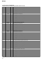
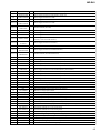
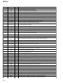
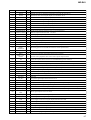
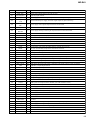
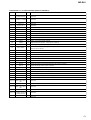
Pin No.
Pin Name
I/O
Description
108
SE
I
Sled error signal input from the RF amplifier
I
Tracking error signal input from the RF amplifier
109
TE
110, 111
AUX1, AUX2
I
Auxiliary A/D input terminal Not used
112
ADRT
I
The upper limit voltage of A/D converter input terminal
113
APC
I
Error signal input terminal for the laser automatic power control Not used
114
ADC1EXTC
-
Connection terminal for an external capacitor (for A/D converter)
115
TEMP_MON
I
Thermistor connection terminal for temperature detection
116
VB_MON
I
Monitor input terminal of rechargeable battery power supply voltage (UNREG)
117
CHG_MON
I
Charge or discharge current monitor input from power control IC
118
VREF_MON
I
Reference voltage monitor input from the RF amplifier
119, 120
SET_KEY_1,
SET_KEY_2
I
Set key input terminal (A/D input)
121
DCIN_DET
I
Monitor input terminal of DC input voltage for battery charge Not used
122
HIDC_MON
I
Monitor input terminal of High DC voltage
123
WK_DET
I
Detection terminal of panel key input for system wake up
124
VBUS_MON
I
Monitor input terminal of USB power supply voltage (VBUS)
125
BATT_MINUS_
MON
I
Monitor input terminal of battery minus terminal
126
RMC_KEY
I
Remote commander key input terminal (A/D input)
127
XHOLD_SW
I
HOLD switch input terminal
128
DRAM_HOLD_
DET
I
Detection terminal for internal D-RAM power supply information keeping
129
JOG_A
I
Jog dial pulse input terminal (A phase) Not used
130
JOG_B
I
Jog dial pulse input terminal (B phase) Not used
131
OPEN_CLOSE_
SW
I
Top panel open/close detection switch input terminal
132
XREC_KEY
I
REC key input terminal
133
XTEST
I
Input terminal for the test mode setting "L": test mode
134
HALF_LOCK_
SW
I
Top panel open switch detection terminal
135
XRST
I
System reset signal input terminal
136
ADC3VREFH
I
Reference voltage input terminal (High voltage)
137
ADC3VREFL
I
Reference voltage input terminal (Low voltage)
138
ADC3EXTC
O
Connection terminal for an external capacitor (for A/D converter)
139
VINP
I
RF signal input from the RF amplifier
140
ADFG
I
ADIP duplex FM signal (19.05kHz to 21.05 kHz) input from the RF amplifier
141
TRDR
O
Tracking servo drive PWM signal output (-) to the coil driver
142
TFDR
O
Tracking servo drive PWM signal output (+) to the coil driver
143
FFDR
O
Focus servo drive PWM signal output (+) to the coil driver
144
FRDR
O
Focus servo drive PWM signal output (-) to the coil driver
145
FS4
O
176.4 kHz clock signal output to the over write head driver and power control IC
146
SLVS
O
Sled servo drive PWM signal output to the motor driver
147
SPDU
O
Spindle motor drive control signal output (U) to the motor driver
148
SPVS
O
Spindle servo drive PWM signal output to the motor driver
149
SPDV
O
Spindle motor drive control signal output (V) to the motor driver
150
SPDW
O
Spindle motor drive control signal output (W) to the motor driver
151
SPCU
I
Spindle motor drive comparison signal input (U) from the motor driver
152
SPCV
I
Spindle motor drive comparison signal input (V) from the motor driver
46