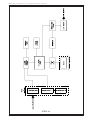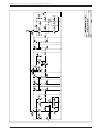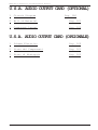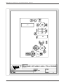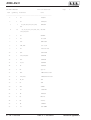
1
RXRL-NV/2
TECHNICAL AND MAINTENANCE MANUAL
MANUALE TECNICO E DI MANUTENZIONE
Manufactured by R.V.R. Elettronica - Italy
RXRL-NV/2 Technical and Maintenance Manual
RXRL-NV/2
Studio Receiver Link 14002600 MHz
Technical and Maintenance Manual
Manuale Tecnico e di Manutenzione
English
Pag. 3
Italiano
Pag. 47
R.V.R. Elettronica S.r.l. (Bo)
Pag. 2
RXRL-NV/2 Technical and Maintenance Manual
INDEX
Preliminary Instructions and Warranty Information
Safety Regulations
Pag. 5
Pag. 7
SECTION 1
General Description
Pag. 10
Electrical Specifications (Table A)
Pag. 12
Dimensional & Environmental Specifications (Table B)
Pag. 13
SECTION 2
Electrical Description
Pag. 14
Front Panel View Description
Pag. 17
Front Panel View (Fig.1)
Pag. 19
Rear Panel View Description
Pag. 20
Rear Panel View (Fig.2)
Pag. 21
Top View Description
Pag. 22
Top View (Fig.3)
Pag. 23
Block Diagram (Fig.4)
Pag. 24
SECTION 3
Installation Procedures
Pag. 25
Recommended Test Equipment (Table C)
Pag. 28
SECTION 4
Maintenance
Pag. 29
SECTION 5
Internal Adjustments
Pag. 34
SECTION 6
Alignment of the Radio Link
Pag. 41
APPENDIX A
Circuit Diagrams, Layouts and Bill of Material
Pag. 92
Wiring Diagram
Pag. 93
Power Supply
Pag. 94
Muting Card
R.V.R. Elettronica S.r.l. (Bo)
Pag. 98
Pag. 3
RXRL-NV/2 Technical and Maintenance Manual
C.P.U.
Pag. 102
Modmeter Card
Pag. 111
Anameter Card
Pag. 116
Audio Process Card
Pag. 124
P.L.L. Card
V.C.O.
Pag. 130
Pag. 135
I.F. 70MHz Card (I.F. 10.7MHz)
Pag. 140
Front-End & Mixer
Pag. 146
Doubler
Inverter Card (Optional)
U.S.A. Audio Output Card (Optional)
Pag. 151
Pag. 155
Pag. 159
Mono-Balance Card (Optional)
Pag. 163
Stereo Decoder Card (Optional)
Pag. 167
R.V.R. Elettronica S.r.l. (Bo)
Pag. 4
RXRL-NV/2 Technical and Maintenance Manual
PRELIMINARY INSTRUCTIONS AND WARRANTY INFORMATION
Please observe safety precautions when handling this unit. This equipment
contains dangerous currents and high voltages.
This manual is written as a general guide for those having previous knowledge
and experience with this kind of equipment. It is not intended to contain a
complete statement of all safety warnings which should be observed by personnel
in using this or other electronic equipment.
R.V.R. doesn’t assume responsibility for injury or damage resulting from
improper procedures or practices by untrained/unqualified personnel in the
handling of this unit.
Please observe all local codes and fire protection standards in the operations
of this unit.
CAUTION:
always disconnect power before opening covers or removing any
part of this unit. Use appropriate grounding procedures to
short out capacitors and high voltage points before servicing.
Any damage to the goods must be reported to the carrier in writing on the
shipment receipt.
Any discrepancy or damage discovered subsequent to delivery, shall be reported
to R.V.R. within five (5) days from its receipt.
R.V.R. extends to the original end-user purchaser all original manufacturers
warranties which are transferable and all claims are to be made directly to
R.V.R. per indicated procedures.
All manufacturers warranties will be supported by R.V.R. to ensure precise
and speedy service where possible.
R.V.R. shall not be liable for any damage of whatsoever nature, arising out
of or in connection with the product or its use thereof.
R.V.R.'s warranty shall not include:
1)
2)
3)
4)
5)
Re-shipment of the unit to R.V.R. for repair purposes
Any unauthorized repair/modification
Incidental/consequential damages as a result of any defect
Nominal non-incidental defects
Re-shipment costs or insurance of the unit or replacement
units/parts
Warranty shall come into force from invoice date and for the period of the
manufactures warranty.
R.V.R. Elettronica S.r.l. (Bo)
Pag. 5
RXRL-NV/2 Technical and Maintenance Manual
To claim your rights under this warranty:
a. Contact the dealer or distributor where you purchased the unit.
Describe the problem and ask if he has an easy solution. Dealers
and Distributors are supplied with all the information about
problems that may occur and usually they can repair the unit quicker
than what the manufacturer could do. Very often installing errors
are discovered by dealers.
b.
If your dealer cannot help you, contact R.V.R. in Bologna and explain
the problem. If it is decided to return the unit to the factory,
R.V.R. will mail you a regular authorization with all the necessary
instructions to send back the goods.
c. When you receive the authorization, you can return the unit. Pack
it carefully for the shipment, preferably using the original packing
and seal the package perfectly. The customer always assumes the
risks of loss (i.e., R.V.R. is never responsible for damage or loss),
until the package reaches R.V.R. premises. For this reason, we
suggest you to insure the goods for the whole value. Shipment must
be
effected C.I.F. (PREPAID) to the address specified by R.V.R.’s
service manager on the authorization.
DO NOT RETURN UNITS WITHOUT OUR AUTHORIZATION AS THEY WILL BE
REFUSED.
Be sure to enclose a written technical report where mention all the problems
found and a copy of your original invoice establishing the starting date of
the warranty.
Replacement and warranty parts may be order from the following address. Be
sure to include the equipment model and serial number as well as part
description and part number.
R.V.R. Elettronica S.r.l.
Broadcasting Equipment Via del Fonditore, 2/2c
40138 Bologna - Italy
-
R.V.R. reserves the right to modify the design and specifications of the
equipment in this manual without previous notice.
R.V.R. Elettronica S.r.l. (Bo)
Pag. 6
RXRL-NV/2 Technical and Maintenance Manual
WARNING!
The currents and voltages in this equipment are dangerous!
Personnel must at all times observe safety regulation!
This manual is intended as a general guide for trained and qualified personnel
who are aware of the dangers inherent in handling potentially hazardous
electrical and electronic circuits.
It is not intended to contain a complete statement of all safety precautions
which should be observed by personnel in using this or other electronic
equipment.
The installation, operation, maintenance and service of this equipment
involves risks both to personnel and equipment, and must be performed only
by qualified personnel exercising due care.
R.V.R. ELETTRONICA S.r.l. shall not be responsible for injury or damage
resulting from improper procedures or from the use of improperly trained or
inexperienced personnel performing such tasks.
During installation and operation of this equipment, local building codes and
fire protection standards must be observed.
WARNING!
Always disconnect power before opening covers,
doors, enclosures, gates, panels or shields.
Always use grounding sticks and short out high
voltage points before servicing. Never make
internal adjustments, perform maintenance or
service when alone or when fatigued.
Do not remove, short-circuit or tamper with interlock switches on access
covers, doors, enclosures, gates, panels or shields.
Keep away from live circuits, know your equipment and don’t take chances.
WARNING!
In case of emergency ensure that power has been disconnected
R.V.R. Elettronica S.r.l. (Bo)
Pag. 7
RXRL-NV/2 Technical and Maintenance Manual
Treatment of electrical Shock
1) If victim is not responsive follow the A-B-C's of basic life support.
PLACE VICTIM FLAT ON HIS BACK ON A HARD SURFACE
A AIRWAY
B BREATHING
IF UNCONSCIOUS,
OPEN AIRWAY
IF NOT BREATHING,
BEGIN ARTIFICIAL
BREATHING.
LIFT UP NECK,
PUSH FOREHEAD BACK,
CLEAR OUT MOUTH IF NECESSARY,
OBSERVE FOR BREATHING
TILT HEAD,
PINCH NOSTRILS,
MAKE AIRTIGHT SEAL,
4 QUICK FULL BREATHS.
REMEMBER MOUTH TO MOUTH
RESUSCITATION MUST BE
COMMENCED AS SOON AS
POSSIBLE.
C CIRCULATION
CHECK CAROTID PULSE
IF PULSE ABSENT,
BEGIN ARTIFICIAL
CIRCULATION
DEPRESS STERNUM 1 1/2" TO 2"
APPROX. 80 SEC. : ONE RESCUER, 15 COMPRESSIONS,
2 QUICK BREATHS.
APPROX. 60 SEC. : TWO RESCUERS, 5 COMPRESSIONS,
1 BREATH
SIONS
NOTE: DO NOT INTERRUPT RHYTHM OF COMPRESWHEN SECOND PERSON IS GIVING BREATH.
Call for medical assistance as soon as possible.
2) If victim is responsive:
a. Keep them warm.
b. Keep them as quiet as possible.
c. Loosen their clothing (a reclining position is recommended).
R.V.R. Elettronica S.r.l. (Bo)
Pag. 8
RXRL-NV/2 Technical and Maintenance Manual
FIRST-AID
Personnel engaged in the installation, operation,
maintenance or servicing of this equipment are urged
to become familiar with first-aid theory and practices.
The following information is not intended to be a
complete first-aid procedure, it is brief and is only
to be used as a reference. It is the duty of all
personnel using the equipment to be prepared to give
adequate Emergency First Aid and thereby prevent
avoidable loss of life.
Treatment of electrical Burns
1) Extensive burned and broken skin.
a. Cover area with clean sheet or cloth.
(Cleansed available cloth article).
b. Do not break blisters, remove tissue, remove adhered particles of
clothing, or apply any salve or ointment.
c. Treat victim for shock as required.
d. Arrange transportation to a hospital as quickly as possible
e. If arms or legs are affected keep them elevated.
NOTE
If medical help will not be available within an hour and the victim is conscious
and not vomiting, give him a weak solution of salt and soda: 1 level teaspoonful
of salt and 1/2 level teaspoonful of baking soda to each quart of water (neither
hot or cold).
Allow victim to sip slowly about 4 ounces (half a glass) over a period of 15
minutes.
Discontinue fluid if vomiting occurs (Do not give alcohol).
2) Less severe burns - (1st & 2nd degree)
a. Apply cool (not ice cold) compresses using the cleansed available
cloth article.
b. Do not break blisters, remove tissue, remove adhered
particles of clothing, or apply salve or ointment.
c. Apply clean dry dressing if necessary.
d. Treat victim for shock as required.
e. Arrange transportation to a hospital as quickly as possible.
f. If arms or legs are affected keep them elevated.
R.V.R. Elettronica S.r.l. (Bo)
Pag. 9
RXRL-NV/2 Technical and Maintenance Manual
SECTION 1
GENERAL
DESCRIPTION
1.1 MECHANICAL DESCRIPTION
The RXRL-NV/2 is housed in a 2U, 19" rack-mounting chassis comprising a
number of interconnected modules mounted internally on the base of the unit.
This allows easy removal and replacement of each module.
The audio output level controls (Mono and Stereo) and meters for various
operating parameters are situated on the front panel.
Mains power, II° I.F. Monitorial Output and R.F. input connectors are mounted
on the rear panel.
1.2 ELECTRICAL DESCRIPTION
The RXRL-NV/2 is a high quality, broadband, FM receiver with a harmonic
distortion better than 0.3%.
The receiver is microprocessor-controlled and synthesized with steps of 100KHz
in the 1400-2600MHz band.
Furthermore, a 15KHz low-pass filter is provided which may be inserted in the
MPX output (always setted on Mono output).
1.3 METERS AND INDICATORS
The receiver’s operating parameters can be measured with the analog
multimeter (21 Fig.1) and the led bar-graph display (18 Fig.1) situated on
the front panel.
The measurement being made by the analog multimeter is indicated by a led
indicator (8 Fig.1) and selectable via the corresponding control
(20 Fig.1).
Peak deviation can be measured with the bar-graph display in steps of 6.6KHz.
The five-figure display (22 Fig.1), mounted centrally, indicates the operating
frequency selected by the UP (14 Fig.1) and DOWN (12 Fig.1) controls and
saveable with the ENTER (13 Fig.1) control.
Three leds provide indication of VCO locked (10 Fig.1), the presence of a stereo
signal (9 Fig.1) and the presence of an SCA signal (11 Fig.1) if the optional
decoder is fitted.
1.4 REMOTE CONTROL (OPTIONAL)
In this equipment an optional serial port (9 pin D-type) is available
allowing remote control of operating frequency and audio muting.
1.5 SPECIFICATIONS
R.V.R. Elettronica S.r.l. (Bo)
Pag. 10
RXRL-NV/2 Technical and Maintenance Manual
Please refer to Table A for the Electrical Specifications and
Table B for the Dimensional and Environmental Specifications.
TABLE A
R.V.R. Elettronica S.r.l. (Bo)
Pag. 11
RXRL-NV/2 Technical and Maintenance Manual
ELECTRICAL
SPECIFICATIONS
A.C. Power
100,120,220 and 240 V ±10%
50-60 Hz, single phase 22W
24 Vdc optional
Cooling
Forced ventilation
Operating frequency
from 1400 to 2600 MHz in
Sub-Bands of 50MHz
Sensitivity
MPX: 1.00mV or less for
60dB SNR
(measured on each
single channel)
Mono: 100µV or less for
65dB SNR
Selectivity
Total harmonic distortion
Stereo separation
Audio outputs
±100 KHz at -3dB
±350 KHz at -70dB
< or = at 0.3%
45 dB, from 40Hz to 15KHz
MPX: +13 dBm, 600 Ohm
unbalanced
Mono: +13 dBm, 600 Ohm
unbalanced
TABLE B
R.V.R. Elettronica S.r.l. (Bo)
Pag. 12
RXRL-NV/2 Technical and Maintenance Manual
DIMENSIONAL AND
ENVIRONMENTAL
SPECIFICATIONS
Chassis Dimensions
82mm (3.22") H
326mm (12.83") D
445mm (17.51") W
Panel Dimensions
483mm (19") W
88mm (3.47") H
Ambient Operating Temperature
from -10°C to +50°C
Humidity
95% maximum, non-condensing
Weight
22,2 Lbs (10 Kg)
R.V.R. Elettronica S.r.l. (Bo)
Pag. 13
RXRL-NV/2 Technical and Maintenance Manual
SECTION 2
ELECTRICAL
DESCRIPTION
2.1 INTRODUCTION
This section describes, in detail, the operating theory of the
RXRL-NV/2.
To aid understanding, the unit has been subdivided into blocks, each of which
is fully described below.
A block diagram is shown in Fig.4.
2.2 POWER SUPPLY
This circuit consists of 1 board mounted on the right side of the chassis
base (7 Fig.3).
The supply is designed to accept line voltages of 100V, 120V, 220V and 240V
±10% (24Vdc optional) at a frequency of 50-60Hz.
The power supply generates the stabilized voltages required by the various
modules comprising the RXRL-NV/2.
After having undergone filtering for mains-borne interference, the supply is
transformed to lower voltages, rectified, smoothed and stabilized for the
following outputs: +5V, +15V and -15V.
The +5V output supplies the CPU card and the PLL card, while the ±15V outputs
supply the CPU card, the Modmeter card, the Anameter cards 1 and 2, the Frontend/Mixer, the Audio Process card, the 70MHz IF card, the PLL, the Muting card
and the Doubler.
All supply voltages may be monitored by the analog multimeter.
2.3 CPU
The CPU is housed in a metal box and mounted on the right side of the front
panel (4 Fig.3).
This circuit converts the number corresponding to the selected operating
frequency into binary code which is written to the programmable dividers of
the PLL.
This allows the VCO to lock to the desired operating frequency.
Several of the receiver’s parameters may be remotely controlled via an optional
9 pin D-type serial port.
In the absence of mains power, a non-volatile memory maintains indefinitely
the last frequency that was programmed.
2.4 MODMETER CARD
R.V.R. Elettronica S.r.l. (Bo)
Pag. 14
RXRL-NV/2 Technical and Maintenance Manual
This card is mounted on the left side of the front panel (1 Fig.3). This
circuit allows the deviation of the signal received by the Audio Process card
(Mono, MPX or SCA).
The card has two BNC connectors; one for the mono signal and the other for
the stereo signal.
A switch allows the gain of the measuring circuit to be set to 10% or 100%
for a more precise reading of low-level deviation (eg. SCA, RDS, pilot tones).
Another switch sets the display mode to bar-graph or peak mode.
The display comprises 14 green leds and 6 red leds.
In the 100% display mode, each led represents 6.66KHz of deviation with the
first red led representing 100KHz and FSD at 130KHz.
In the 10% mode, each led represents 0.66KHz of deviation.
2.5 ANAMETER CARD
This circuit comprises two cards and a meter mounted centrally on the front
panel (3 Fig.3).
This sub-assembly displays the values of various operating parameters of the
receiver: internal voltages and signal levels of MONO, MPX, STEREO, SCA, CENTER
(signal centering) and SIGNAL (signal amplitude).
The parameters are selected by a lever switch (20 Fig.1) and the selection
is indicated by the legend of the green led (8 Fig.1).
The readings are taken using the corresponding scale:
MEASUREMENT
Internal voltages
Signal levels
SCALE
FDS
V
V
30V
1mV
Three green leds indicate the presence of a STEREO signal, P.L.L. lock and
the presence of a SCA signal (SCA PRES. and STEREO PRES. leds are working only
with the option decoder fitted).
2.6 FRONT-END & MIXER
These cards are housed in an aluminum billet (2 Fig.3) and are mounted
on the front part of the metal container enclosing the Audio Process and 70
MHz IF cards.
The Front-End section receives the RF signal from the RF cavity, filters and
amplifies it.
The Mixer section receives the RF signal from the Front-End circuit and mixes
it with the signal generated by the Doubler.
The difference signal obtained is supplied to the 70 MHz IF card.
2.7 CAVITY FILTER
This cavity filter (9 Fig.3) is screwed to cover of the metal container
R.V.R. Elettronica S.r.l. (Bo)
Pag. 15
RXRL-NV/2 Technical and Maintenance Manual
housing the Audio Process and 70MHz IF cards.
The receiver's RF cavity is used to privilege its working frequency.
2.8 PLL
This card (13 Fig.3) is mounted on the left side of the base of the unit.
The VCO (12 Fig.3) is mounted on this card, enclosed in a metal container.
This circuit receives the R.F. signal and reads the binary equivalent of the
frequency supplied by the CPU.
The PLL compares the reference signal to the VCO signal and uses the difference
to lock the VCO to the operating frequency.
2.9 AUDIO PROCESS CARD
This card is mounted in the rear of the metal container situated in the
center of the unit.
The Audio Process card processes the various audio signals such as MONO, MPX,
SCA and RDS coming from the 70 MHz IF card.
Furthermore, it supplies these processed signals to the various instruments
found on the Anameter and Modmeter cards.
The card also provides a signal for the Muting card which displays the muting
status and allows the adjustment of the threshold (factory calibrated to
approx. -83 dBm).
2.10 70MHz IF CARD
This card is mounted at the front of the metal container situated in the
center of the unit.
The circuit receives a 70MHz input which is filtered, amplified and then mixed
with a 59.3MHz signal generated by a crystal oscillator.
The resultant 10.7MHz signal, being the difference of the above card for
processing.
2.11 MUTING CARD
This card is mounted on the right side of the front panel and allows
adjustment of the receiver’s muting threshold (= -83 dBm of default) and
displays the muting status with a led (16 Fig.1).
2.12 DOUBLER
This circuit (6 Fig.3) is screwed to the cover of the metal container
housing the Audio Process and 70 MHz IF cards. The circuit doubles the frequency
of the VCO output at a level of about +7 dBm, and the output is supplied to
the input of the Mixer which combines it with the R.F. signal.
The resultant 70 MHz signal is then supplied to the 70 MHz IF card.
R.V.R. Elettronica S.r.l. (Bo)
Pag. 16
RXRL-NV/2 Technical and Maintenance Manual
FRONT PANEL VIEW DESCRIPTION (FIG.1)
1
LEVEL HEAR
Hear level trimmer
2
HEAR
Hear jack
3
MONO
Mono output connector, BNC type
4
MONO LEVEL TRIMMER
Mono Level Trimmer
5
STEREO LEVEL TRIMMER
6
MPX
7
ON/OFF LPF\15KHz
8
LEDS
9
STEREO PRES.
Stereo Level Trimmer
Stereo output connector, BNC type
ON/OFF Low Pass Filter selector
Light indicator indicated which
parameter of the receiver is being
displayed on the analog meter
STEREO signal led indicator (only
with STEREO internal decoder
included)
10
LOCK
This indicator will light when the
VCO is locked to the reference
frequency
11
SCA PRES.
SCA signal led indicator (only
with SCA internal decoder
included)
12
DOWN
13
ENTER
14
UP
Control frequency display.
Any momentary pushes causes the
digit to go down 100KHz a time
Enters the frequency on the
display into microprocessor and
memory. Once entered, the
frequency is stored until a new
frequency
is entered on the front
panel even if the
power is turned
off for several days
Controls the display frequency in
the same way as the "DOWN" button,
except that the frequency goes up
in 100KHz steps
15
LEVEL MUTING
Muting Level Trimmer
R.V.R. Elettronica S.r.l. (Bo)
Pag. 17
RXRL-NV/2 Technical and Maintenance Manual
16
MUTING
Muting led indicator
17
BAR/DOT
Selector of operation mode
(BAR/DOT) for deviation meter
18
DEVIATION
Deviation meter by "Led Diode
19
x1/x10
Bar"
Expansion of modulation meter
scale:
Pos. X1 - Full scale shows 100%
Pos. X10 Full scale shows 10%
20
METER SELECTOR
Pushing the switch each time will
light on led at a time in upward
direction
21
METER
Analog meter used to monitor the
parameters of the receiver such
as:
+15V
+5V
EXT 24V
SIGNAL
CENTER
SCA
MONO
MPX
22
FREQUENCY DISPLAY
23
ON
24
POWER
R.V.R. Elettronica S.r.l. (Bo)
Frequency indicator
ON/OFF Power Switch Led
ON/OFF Power Switch
Pag. 18
RXRL-NV/2 Technical and Maintenance Manual
FIG.1
R.V.R. Elettronica S.r.l. (Bo)
Pag. 19
RXRL-NV/2 Technical and Maintenance Manual
REAR PANEL VIEW DESCRIPTION (FIG.2)
1
PLUG
A.C. power plug
2
FUSE BLOCK
3
REMOTE CONTROL
Fuse Block & Voltage Changer. Use
a small screwdriver to change fuse
or volt age setting. Turn block
and place desired operating
voltage
next to arrow
DB9 communication line to control
or receive status of the receiver.
Baud rate is 1200 Baud.
On request, it may be changed to
300, 600 or 2400 baud.
A program is available on 5 1/4"
or 3 1/2" disk for IBM ® or
compatible.
Plug is a standard DB9 female.
Pin
Pin
Pin
Pin
Pin
Pin
Pin
Pin
Pin
1
2
3
4
5
6
7
8
9
Not
TXD
RXD
DSR
GND
DTR
CTS
RTS
Not
Connected
*
*
$
$
Connected
* DTR and DSR are connected
together
$ CTS and RTS are connected
together
4
(+) EXT 24V
(Optional)
Positive terminal for EXT 24
5
(-) EXT 24V
6
U.S.A. Audio Output (Optional)
7
FAN
Cooling fan
8
TEST POINT 10.7MHz
Test point connector 10.7MHz
9
VOLTAGE REGULATOR 1
Voltage regulator for +5V
10
VOLTAGE REGULATOR 2
Voltage regulator for +15V
11
R.F. INPUT
50 Ohm, "N" Connector
(Optional)
R.V.R. Elettronica S.r.l. (Bo)
Negative terminal for EXT 24V
U.S.A. audio outputs for telemetry
Pag. 20
RXRL-NV/2 Technical and Maintenance Manual
FIG.2
R.V.R. Elettronica S.r.l. (Bo)
Pag. 21
RXRL-NV/2 Technical and Maintenance Manual
TOP VIEW DESCRIPTION (FIG.3)
1
.............. Modulation Meter & Mono/Mpx Output Board
2
.............. Front-End & Mixer
3
.............. Anameter Card
4
.............. C.P.U.
5
.............. Transformer
6
.............. Doubler
7
.............. Power Supply
8
.............. Supply Socket
9
.............. R.F. Cavity
10
.............. Fan
11
.............. R.F. Input Connector
12
.............. V.C.O.
13
.............. P.L.L. Card
R.V.R. Elettronica S.r.l. (Bo)
Pag. 22
RXRL-NV/2 Technical and Maintenance Manual
FIG.3
R.V.R. Elettronica S.r.l. (Bo)
Pag. 23
RXRL-NV/2 Technical and Maintenance Manual
FIG.4
R.V.R. Elettronica S.r.l. (Bo)
Pag. 24
RXRL-NV/2 Technical and Maintenance Manual
SECTION 3
INSTALLATION PROCEDURE
3.1 INTRODUCTION
This chapter contains the information required to install the
RXRL-NV/2 and carry out preliminary checks.
3.2 UNPACKING
Remove the unit from its packing and, before anything else, ensure that
the unit has not suffered any damage during transit and that all front and
rear panel controls are operational.
3.3 INSTALLATION
To install the RXRL-NV/2 receiver, carry out the following procedure:
1)
This receiver is able to operate from 4 different supply voltages:
100, 120, 220 or 240Vac, at 50-60Hz.
First of all select the correct supply voltage using the selector
situated on the rear panel; use a screwdriver to raise the cover
(2
Fig.2) on which are the various voltages, rotate it until the
arrow
points to the correct voltage and re-insert it.
Check that a fuse is fitted to the cover and that its value
corresponds to the following:
220-240Vac 1A
100-120Vac 2A
2)
Ensure that the antenna is correctly fitted to the R.F. input
(11 Fig.2) situated on the receiver’s rear panel.
3)
Switch the power switch (24 Fig.1) to the OFF position.
4)
Connect power to the unit via the VDE socket (1 Fig.2).
NOTE: It is essential that the unit be properly earthed to ensure both the
safety of the operator as well as the correct functioning of the equipment.
5) Switch the power switch to the ON position and check that the green
POWER ON led (23 Fig.1), and the green led corresponding to the
parameter selection SIGNAL (8 Fig.1), are both lit.
After a few seconds the frequency display (22 Fig.1) will come on
and display a number (eg. 1750.00) corresponding to the last
operating frequency to have been programmed.
The green LOCK led should switch on within 30 seconds indicating
R.V.R. Elettronica S.r.l. (Bo)
Pag. 25
RXRL-NV/2 Technical and Maintenance Manual
that the oscillator has locked to the operating frequency displayed.
The display has five digits, 4 before the decimal point representing
(from left to right) thousands of MHz, hundreds of MHz, tens of MHz
and MHz; and 1 after the decimal point representing hundreds of KHz.
To change this number, use the UP (14 Fig.1) and DOWN (12 Fig.1)
buttons to respectively increase it and decrease it.
Once the desired frequency has been found, press ENTER (13 Fig.1)
to confirm and save it.
As soon as the ENTER button has been pressed, the LOCK led will switch
off (providing that the new frequency is different from the old),
indicating that the VCO is re-tuning to the new frequency.
If the ENTER is not pushed, the display will flash the new value
four times and then reset to the previous value.
NOTE: The receiver will continue to function normally at the same frequency,
throughout the procedure described above, until the ENTER button is pressed.
Note that a momentary press of the UP and DOWN buttons will increment
or decrement the right most digit by 1 (corresponding to a frequency
change of 100KHz).
A longer press of either button will cause the display to increment
or decrement continuously until the button is released.
Furthermore, when the limit of the operating frequency band is
reached, the displayed frequency will jump to the other limit and
carry on changing in the direction corresponding to the button being
pushed.
NOTE: The frequency band is pre-defined by the user and rarely exceeds 50 MHZ.
Example: Band 1750-1800 MHz:
UP button pressed:
1799.99 1800.00 1750.00 1750.10
DOWN button pressed: 1750.10 1750.00 1800.00 1799.99
After the PLL has been locked for about 90 seconds, the display turns
off automatically.
To switch it on, press the ENTER button.
6)
Connect an audio analyzer to the MONO (3 Fig.1) or MPX outputs
(6 Fig.1).
Using an R.F. signal generator, inject a carrier at the receiver’s
operating frequency into the R.F. input of the receiver, at a level
of
-47dBm.
Modulate the carrier with a 400Hz tone at a deviation of ±100KHz.
Check that the analog meter (21 Fig.1) displays a reading of 1mV.
7) Select CENTER with the selector (20 Fig.1) and check that the
received signal is centered.
8) Deviation meter check.
Set the modulation display gain (20 Fig.1) to 130% f.s.d.
Connect an audio analyzer to the MONO output (3 Fig.1).
Check that the bar-graph display (18 Fig.1) lights up to the first
R.V.R. Elettronica S.r.l. (Bo)
Pag. 26
RXRL-NV/2 Technical and Maintenance Manual
red led, indicating 100% deviation (equivalent to 100 KHz).
With the DOT/BAR switch in the bar position, all the green leds and
first red led will be on.
Check that the audio analyzer reads +13dBm.
9)
Connect an audio analyzer to the STEREO output (6 Fig.1).
Inject an externally generated carrier at the receiver’s operating
frequency, modulated by a 10KHz tone with ±100KHz deviation, into
the receiver’s R.F. input.
Check that, as for the MONO channel, the first red led switches on.
Check also that the level measured by the audio analyzer is 2.5dBm
for the version with 50µsec de-emphasis and -1dBm for the version
with 75µsec de-emphasis.
10) Inject a signal with a level of -83dBm and adjust the MUTING trimmer
R2 (15 Fig.1) until the red muting led switches on.
The audio signal will be automatically disabled and the Modmeter
bar-graph display will go out.
Using a pair of headphones, check that the audio has indeed been
disabled and that no signal remains audible.
If the audio level rises, the MUTING led will go out and reception
will continue as before.
11) The correct functioning of the STEREO PRES. led can only be verified
if the optional Stereo Decoder is fitted.
Similarly, the SCA PRES. led can only be checked if an optional SCA
decoder is fitted and a SCA signal is being received.
TABLE C
RECOMMENDED TEST EQUIPMENT
R.V.R. Elettronica S.r.l. (Bo)
Pag. 27
RXRL-NV/2 Technical and Maintenance Manual
INSTRUMENT
MODEL
SPECIFICATIONS
Non-inductive
dummy load
Bird
50 Ohm P > 5W
Spectrum Analyzer
Advantest
Mod. R4141D
F.M. Modulation Meter
Rohde Schwarz
Mod. F.A.M.
Digital Multimeter
Metrix
Power Meter
Hewlett Packard
Mod. 435B
Stereo Decoder
A.E.V.
Mod. SMD
Low Distortion
A.F. generator
Krohn-Hite
Mod. 4400A
Oscilloscope
Tektronix
DC-20MHz
R.F. Generator
Rohde Schwarz
Mod. SMPD
5KHz / 2720MHz
Audio Analyzer
Panasonic
Mod. 2247A
30dB Attenuator
Hewlett Packard
Mod. 8498A
Variable Attenuator
Hewlett Packard
Mod. 8496B
Variable Attenuator
10KHz - 3.5GHz
Stereo separation
> 60dB 30Hz to 15KHz
THD < 0.001%
Max Avg Pwr 30W
Attenuator 110dB
Max RF Pwr 1W CW
Hewlett Packard
Attenuator 11dB
Max RF Pwr 1W CW
SECTION 4
MAINTENANCE
R.V.R. Elettronica S.r.l. (Bo)
Pag. 28
RXRL-NV/2 Technical and Maintenance Manual
4.1 SAFETY REQUIREMENT
WARNING WARNING WARNING WARNING WARNING WARNING WARNING
When the receiver is operational, removing the top panel will expose lethal
voltages on the line voltage selector.
Use insulated tools for any type of adjustment and do not touch any internal
component with the unit switched on.
Ensure that the unit is disconnected from all sources of power before carrying
out any inspection or maintenance work.
MAINTENANCE LEVEL 1
4.2 ROUTINE MAINTENANCE
The only routine maintenance required by the RXRL-NV/2 is the periodic
replacement of the cooling fan and the removal of accumulated dust.
The period between such action will depend on ambient operating conditions
such as temperature, air-borne dust levels and humidity.
It is advisable to check the unit every 6 months and to replace noisy or worn
fans.
Fans should be replaced as a meter of course after no more than 18 months of
operation.
MAINTENANCE LEVEL 2
4.3 CPU REPLACEMENT
1)
Open the top cover of the unit.
2)
Disconnect connectors CN1 and CN1 that connect the CPU to the P.L.L.
card and the RS232C connector, respectively.
3)
Undo the screws holding the front panel in place.
4) Undo the nuts holding the front panel switches in place and remove
the CPU.
5)
Remove the card with great care.
6) Undo the screws holding the CPU’s protective metal container, and
remove the cards.
4.4 ANAMETER CARD REPLACEMENT
1)
Open the top cover of the unit.
2)
Undo the front panel fixing screws.
R.V.R. Elettronica S.r.l. (Bo)
Pag. 29
RXRL-NV/2 Technical and Maintenance Manual
3) Disconnect connector CN1 connecting the Anameter card to the Audio
Process card.
4)
Undo the nut holding the selector switch in place on the front panel.
5)
Unscrew the nuts holding the card to the meter.
6)
Remove the card with great care.
4.5 MODMETER CARD REPLACEMENT
1)
Open the top cover of the unit.
2)
Disconnect connector CN1.
3)
Undo the front panel fixing screws.
4) Disconnect the 2 pole connector connecting the Modmeter card to the
LEVEL HEAR connector situated on the front panel.
5) Undo the MONO and MPX connector fixing nuts and the switch fixing
nuts on the front panel.
6)
Slide the card out with great care.
4.6 POWER SUPPLY REPLACEMENT
1)
Open the top cover of the unit.
2)
Disconnect connector CN6.
3)
Disconnect the connector block CN5.
4) Take careful note of the position of each cable with reference to
its color.
5) Disconnect the faston connectors (CN1, CN2, CN3, CN4) connecting
the transformer to the bridge rectifier.
6)
Remove the screws fixing the card to the chassis.
7)
Remove the Power Supply with great care.
4.7 FRONT-END AND MIXER REPLACEMENT
1)
Open the top cover of the unit.
2)
Disconnect connectors CN1, CN2 e CN3.
R.V.R. Elettronica S.r.l. (Bo)
Pag. 30
RXRL-NV/2 Technical and Maintenance Manual
3)
Desolder the power cable.
4) Unscrew the Front-End/Mixer from the cover of the metal container
protecting the Audio Process and 70MHz IF cards.
5)
Remove the Front-End/Mixer with great car
4.8 P.L.L. REPLACEMENT
1)
Open the top cover of the unit.
2)
Desolder the wire connecting the PLL to the Doubler.
3)
Disconnect connectors CN1, CN2 and CN3.
4)
Undo the nuts fixing the PLL card in place.
5)
Remove the PLL with great care.
4.9 MUTING CARD REPLACEMENT
1)
Open the top cover of the unit.
2)
Disconnect connector CN0.
3)
Undo the nut fixing the LEVEL MUTING trimmer to the front panel.
4)
Remove the Muting card with great care.
4.10 AUDIO PROCESS CARD REPLACEMENT
1)
Open the top cover unit.
2) Open the cover of the metal container which protects the Audio
Process card and the 70MHz IF card and it will also be necessary
disconnect the Front-End, the Mixer and Doubler connectors fixed
the cover.
3) Take note of the position of the various connectors of the Audio
Process and 70MHz IF cards.
4) Disconnect connectors CN1, CN2, CN3 and CN4 from the Audio Process
card and connectors CN2, CN3, CN4, CN5 and CN6 from the 70MHz IF
card, the latter to facilitate removal.
5) Undo the nuts holding the card in place and remove the card with
the great care.
R.V.R. Elettronica S.r.l. (Bo)
Pag. 31
to
to
RXRL-NV/2 Technical and Maintenance Manual
4.11 70MHz IF CARD REPLACEMENT
1)
Open the top cover of the unit.
2) Open the cover of the metal container which protects the Audio
Process card and the 70MHz IF card and disconnect the Front-End,
the Mixer and Doubler connectors fixed to the cover.
3) Take note of the positions of the various connectors of the Audio
Process and 70MHz IF card.
4) Disconnect connectors CN1, CN2, CN3 and CN4 from the Audio Process
card and connectors CN2, CN3, CN5, CN5 and CN6 from the 70MHz IF
card.
5)
Undo the nuts holding the 70MHz IF card in place.
6)
Remove the card with great care.
4.12 V.C.O. REPLACEMENT
1)
Open the top cover of the unit.
2)
Disconnect connectors CN1, CN3 and CN4 of the P.L.L. Card.
3)
Desolder the power cable coming from the P.L.L..
4)
Desolder the metal box from upper cover.
5)
Remove the V.C.O. with great care.
4.13 DOUBLER REPLACEMENT
1)
Open the top cover of the unit.
2)
Disconnect connectors CN1 and CN2.
3)
Desolder the Doubler power supply cable.
4)
Unscrew the Doubler from cover of the metal container which protects
the Audio Process card and the 70MHz IF card.
5)
Remove the Doubler with great care.
4.14 R.F. CAVITY REPLACEMENT
1)
Open the top cover of the unit.
2)
Disconnect connectors of the R.F. cavity.
R.V.R. Elettronica S.r.l. (Bo)
Pag. 32
RXRL-NV/2 Technical and Maintenance Manual
3) Unscrew the R.F. Cavity from the cover of the metal container
which protects the Audio Process card and the 70MHz IF card.
4)
Remove the R.F. Cavity with great care.
SECTION 5
CALIBRATION PROCEDURE OF
R.V.R. Elettronica S.r.l. (Bo)
Pag. 33
RXRL-NV/2 Technical and Maintenance Manual
MODULES
5.1 INTRODUCTION
TO ENSURE AN ACCURATE CALIBRATION OF THE RECEIVER, ALLOW THE UNIT TO REACH
NORMAL OPERATING TEMPERATURE BEFORE CALIBRATION
5.2 CALIBRATION OF THE R.F. CAVITY
To carry out this procedure, connect the transmitter and receiver as showed
in SETUP 1 (Fig.5):
SETUP 1 / FIG. 5
1) Adjust the variable attenuator for a value dependent from the
transmitter's output power (Table E).
2)
Calibrate the R.F. Cavity, situated on the receiver, for the maximum
R.F. signal, checking against the corresponding reading on the
receiver’s meter (maximum R.F. signal displayable = -47dBm).
5.3 CALIBRATION OF THE
FRONT-END AND MIXER
The Front-End/Mixer module is presetted on working frequency by factory.
In case in which is necessary to change frequency band, send the module to
the factory for the re-adjustement because this setting is very difficult.
5.4 CALIBRATION OF THE 70MHz IF STAGE
To carry out this procedure, configure the unit as detailed in
SETUP 2 (Fig.6):
R.V.R. Elettronica S.r.l. (Bo)
Pag. 34
RXRL-NV/2 Technical and Maintenance Manual
1) Use an R.F. signal generator to inject a -47 dBm signal into the
R.F. input of the receiver.
SETUP 2 / FIG. 6
2) Using a frequency meter, check the accuracy of the 10.7 MHz IF
(10.700 MHz is acceptable).
Adjust if necessary using compensators C27 and C28 situated on the
PLL card.
3)
Using an oscilloscope, adjust TR1 and then TR2, situated on the card,
to maximize the 10.7 MHz IF signal level.
4)
Check that the amplitude of the 10.7 MHz IF signal is still 150 mVpp,
and if not, adjust P1 accordingly (take care adjusting P1 not to
increase distortion levels).
5)
Now configure the receiver as detailed in SETUP 3 (Fig.7).
6) Inject a 400 Hz tone into the R.F. generator and modulate it with
a deviation of ±100 KHz. The resultant output should be fed to the
SETUP 3 / FIG. 7
R.F. input of the receiver.
7) Check that the MONO (R42) and STEREO (R41) trimmers, situated on
the front panel, are in their maximum position.
8) Measure the MONO signal level output by the receiver into the
audio signal analyzer.
9)
Adjust TR3 for the maximum value and TR4 for the minimum.
10) Set the audio analyzer to a measure audio distortion percentage with
a low-pass filter at 30 KHz.
11) Adjust TR3 and TR4, alternately, to obtain the minimum MONO
distortion figure (typically 0.1%). Having optimized the MONO
figure, the STEREO figure should also be optimized (typically 0.3%).
If this is not the case, adjust P1, TR1 and TR2, taking care not
R.V.R. Elettronica S.r.l. (Bo)
Pag. 35
RXRL-NV/2 Technical and Maintenance Manual
to reduce excessively the amplitude of the 10.7 MHz IF signal.
5.5 CALIBRATION OF THE MUTING CARD
To carry out this procedure, configure the unit as detailed in
SETUP 4 (Fig.8).
1)
Inject a -83 dBm signal into the R.F. input of the receiver.
4 / on
FIG.
2) Adjust potentiometer SETUP
P2, situated
the 708 MHz IF card, to its
halfway position.
3) Adjust trimmer R2, situated on the MUTING card, until the receiver
disables the audio signal.
5.6 CALIBRATION OF THE AUDIO PROCESS CARD
To carry out this procedure, configure the unit as detailed in
SETUP 3 (Fig.7).
1) Check that trimmers R41 and R42, corresponding to the MONO and MPX
outputs, are at maximum.
2) Check that jumper JP1 is in the correct position for the desired
de-emphasis (position A = 50µs European version; position B = 75µs
American version).
3) Inject a signal with the carrier at the receiver’s operating
frequency and modulated with 400 Hz at ±100 KHz deviation.
4) Adjust R8 to obtain a reading on the audio analyzer of +13dBm for
the MONO input.
5)
Now inject a 10 KHz signal with a deviation of 100 KHz.
Adjust R12 for a reading of 2.5 dBm for 50µs de-emphasis (-1dBm for
75µs de-emphasis).
6) Inject a carrier at the receiver’s operating frequency, modulated
by a 400 Hz tone with a deviation of ±100 KHz.
7)
Check that the signal level is still +13 dBm and if not, adjust R8.
R.V.R. Elettronica S.r.l. (Bo)
Pag. 36
RXRL-NV/2 Technical and Maintenance Manual
8) Use the Modmeter calibration procedure to ensure that the readings
are correct.
9) It is essential to calibrate the MONO signal before being able to
accurately measure MPX.
10) Configure the unit as detailed in SETUP 5 (Fig.9).
11) Insert the 15 KHz low-pass filter (7 Fig.1).
SETUP
/ FIG.
9
12) Adjust R18 to obtain a
signal 5
level
of +13 dBm.
13) Disable the 15 KHz low-pass filter and adjust R15 for a signal level
of +13dBm.
14) Configure the unit as detailed in SETUP6 (Fig.10) to measure stereo
separation.
15) If the Stereo Decoder has an OVER RANGE indicator, adjust the stereo
output level until the indicator just switches off.
SETUP 6 / FIG. 10
16) Inject a carrier at the receiver’s operating frequency, modulated
by a 10KHz tone with a deviation of ±100 KHz.
17) Check that the stereo separation reading is around 40-45 dB for both
channels.
If this is not the case, adjust R80 and R65 ensuring that the stereo
separation is balanced for both channels (±2 or 3 dB between L/R
R.V.R. Elettronica S.r.l. (Bo)
Pag. 37
RXRL-NV/2 Technical and Maintenance Manual
and R/L).
18) Inject a carrier at the receiver’s operating frequency, modulated
by a 400 Hz tone with a deviation of ±100 KHz.
19) If necessary, adjust R71 to improve the stereo separation, using
the procedure described in step 16.
20) Inject a modulation signal with a frequency from 40Hz to 15KHz and
verify that the stereo separation is always grater than 40dB.
5.7 CALIBRATION OF THE CPU
After replacement, check that the displays function and that operating
frequencies can be programmed using the UP (14 Fig.1), DOWN (12 Fig.1) and
ENTER (13 Fig.1) buttons.
Check correct operation of the RS232 serial port (if fitted).
No other checks are required.
5.8 CALIBRATION OF THE ANAMETER CARD
For each of the selector positions adjust the corresponding trimmer for
the values listed below:
READING
VALUE
+15V
15V
+5V
5V
EXT 24V (OPT) 24V
SIGNAL
1mV
CENTER
BLACK MARK
SCA
MONO
MPX
FSD
TRIMMER
30V
30V
30V
1mV
NOTE
R18
R17
R22
R21
R16
R15
1
2
R19
R20
3
4
NOTE:
1) The reading is valid at the half-way point on the horizontal black
mark on the meter scale.
2) If the receiver does not have a dedicated SCA output, it is not
possible to measure the SCA level on the Modmeter.
If present however, inject a 67-70 KHz signal with a deviation of
10KHz, select SCA measurement with the front panel selector and
select x10 with the Modmeter selector.
Configure the unit as detailed in SETUP 7 (Fig.11).
R.V.R. Elettronica S.r.l. (Bo)
Pag. 38
RXRL-NV/2 Technical and Maintenance Manual
Adjust trimmer R28, situated on the Audio Process card, to obtain
a reading of 0 dBm. Adjust
R15 so 7that
first
SETUP
/ the
FIG.
11red led of the
bar-graph display switches on.
3)
Configure the unit as detailed in SETUP8 (Fig.12).
Put the bar-graph display selector in position x1 and inject a
carrier at the receiver’sSETUP
operating
by a 400Hz
8 frequency
/ FIG. modulated
12
tone with a deviation of ±100 KHz.
Check that the first red led switches on and if not, adjust R19
accordingly.
4) Repeat the procedure detailed in note 3 to measure the MPX signal.
Carry out all the calibration procedures for the various parameters
and select a measurement other than SCA, MONO or MPX.
Select x10 on the Modmeter and inject a carrier at the receiver’s
operating frequency, modulated by a 400Hz tone with ±10KHz deviation
and re-check that the first red led of the bar-graph display is
switched on.
Adjust R4 if necessary.
5.9 CALIBRATION OF THE MODMETER CARD
For this procedure please refer to SETUP8 (Fig. 12).
1) Inject a carrier at the receiver’s operating frequency, modulated
by a 400Hz tone with 100KHz deviation.
2)
Set the switch to the "x1" position.
3)
Adjust trimmer R30, situated on the Modmeter card, so that the first
red led switches on (corresponding to the 100% mark).
4) Set the switch to the "x10" position.
5) Inject a carrier at the receiver’s operating frequency, modulated
by a 400Hz tone with ±10KHz deviation.
6)
Adjust trimmer R4, situated on the Modmeter card, so that the first
R.V.R. Elettronica S.r.l. (Bo)
Pag. 39
RXRL-NV/2 Technical and Maintenance Manual
red led switches on (corresponding to the 100% mark).
5.10 CALIBRATION OF THE POWER SUPPLY
This module does not require calibration.
5.11 CALIBRATION OF THE VCO
To calibrate the VCO, carry out the following procedure:
1) Connect the positives probe of a voltmeter to the glass capacitor
P2 (connected to the varicap) and the negative probe to ground.
2) Check that at both limits of the operating frequency band (defined
by the EPROM), the voltage reading lies between 3.5 and 10.3V.
The higher frequency should correspond to the higher voltage and
vice versa.
3) If the voltages in step 2. cannot be verified i.e. the PLL is not
locked, the soldered joint, connecting the SL strip-line to ground,
should be moved (the other end of the strip-line is connected to
the cathode of the varicap via capacitor CX).
4) If the calibration procedure is being carried out after a change
of frequency, capacitor CX and impedance L4, situated on the VCO
card, will also have to be changed according to Table D.
5.12 CALIBRATION OF THE DOUBLER
This module does not require calibration. In the event of replacement,
new modules are supplied factory-calibrated.
R.V.R. Elettronica S.r.l. (Bo)
Pag. 40
RXRL-NV/2 Technical and Maintenance Manual
SECTION 6
ALIGNMENT OF THE RADIO
LINK
6.1 INTRODUCTION
This chapter details the alignment procedure for the PTRL-NV/2 (or PTRLNV/2/HP) transmitter and the RXRL-NV/2 receiver.
6.2 FREQUENCY ALIGNMENT
The operating frequency of the complete radio link (TX+RX) is set using
a frequency meter to measure the frequency output by the transmitter and the
frequency after the second conversion of the receiver.
It is recommended to align both units (TX and RX) at the same time and with
the same frequency meter, preferably on of high precision
(eg. ±0.2ppm).
A difference of >2 KHz between the transmitter’s center frequency and that
of the receiver (measured at the intermediate frequency of 10.7MHz) will result
in degradation of audio quality and stereo separation.
To perform this alignment, carry out the following procedure (SETUP A1 and
A2):
1)
Connect the transmitter as shown in SETUP A1 (Fig.7).
SETUP A1 / FIG. 7
R.V.R. Elettronica S.r.l. (Bo)
Pag. 41
RXRL-NV/2 Technical and Maintenance Manual
2) Switch on the transmitter and wait until it has locked to its
operating frequency i.e. the UNLOCK light goes out.
3) Connect a 30dB attenuator between the R.F. Output and 50 Ohm and
Frequency Counter.
4) Use the meter selector to select direct power measurement, FWD.
Check that maximum output power.
5) Using the frequency meter, check the output frequency of the
transmitter and adjust as necessary with capacitors C68 and C69
situated on the Main card.
6)
Connect the two units (TX and RX) as shown in SETUP A2 (Fig.8).
SETUP A2 / FIG. 8
7) Adjust the variable attenuator for a value dependent from the
transmitter’s output power (Table E).
8) Connect the counter to the IF 10.7MHz output and check that the
frequency corresponds to this value, adjusting as necessary with
capacitors C27 and C28 situated on the Synthesizer card for a
frequency of 10.700MHz ±2KHz.
6.3 MEASUREMENT OF RECEIVER S/N RATIO
The mono S/N (signal to noise) ratio is measured at the output of the
receiver by feeding it with a 400Hz modulating signal (±100KHz deviation) and
comparing the output with the same output, under the same conditions, in the
absence of the modulating signal, across the 30Hz/20KHz band.
In the case of stereo modulation, the S/N ratio will be measured on single
channels (left and right) decoded and de-emphasized.
Both mono and stereo measurements should be taken having configured the unit
according to SETUP B1 and B2 and carrying out the following procedure:
R.V.R. Elettronica S.r.l. (Bo)
Pag. 42
RXRL-NV/2 Technical and Maintenance Manual
1) Connect the instruments as shown in SETUP B1 (Fig.9) to make
the MONO measurement.
SETUP B1 / FIG. 9
2)
Generate an R.F. carrier at operating frequency and -67dBm; modulate
the carrier with a 400Hz tone with a ±100KHz deviation.
Inject the resultant R.F. signal into the receiver input.
3) Using the "FAM" modulation analyzer, check that the S/N ratio or
the RXRL-NV/2 receiver is better than 65dB, referred to a deviation
±100KHz.
4) Connect the instruments as shown in SETUP B2 (Fig.10) to make the
STEREO measurement.
SETUP B2 / FIG. 10
5) Adjust the signal generator output for a level of 1mV (the carrier
and deviation will remain constant).
R.V.R. Elettronica S.r.l. (Bo)
Pag. 43
of
RXRL-NV/2 Technical and Maintenance Manual
6) Use the modulation analyzer to make the S/N measurement and check
that the figure is better than 60dB (measured on each demodulated
and de-emphasize single channel) for the RXRL-NV/2 receiver.
6.4 STEREO SEPARATION
Stereo separation is measured using a stereo coder, a stereo demodulator
and an audio analyzer. The figure is obtained from the ratio of the left and
right channel outputs with only the left (or only right) channel modulated,
for frequencies between 30Hz and 15KHz.
To make this measurement, configure the unit according to SETUP C
(Fig.11) and carry out the following procedure:
SETUP C / FIG. 11
1) Adjust the variable attenuator for a value dependent from the
transmitter’s output power (Table E).
2) Adjust the audio generator for an output level of -10dBm at the
right input (and subsequently the left) of the stereo coder.
3) Check that the reading from the output of the stereo decoder is
better or equal to 40dB (both at 40Hz and 15KHz).
4) Repeat the operation for both channels with a modulating tone of
400Hz and 10KHz. The maximum difference should be ±3dB.
6.5 CHANGING FREQUENCY
The are two different procedures for changing frequency, depending on the new
frequency to be selected:
CASE A - Should the new frequency fall within the range of receiver's
R.F. Power Amplifier Stage (and relative receiver's Front-End/
Mixer)
R.V.R. Elettronica S.r.l. (Bo)
Pag. 44
RXRL-NV/2 Technical and Maintenance Manual
CASE B - Should the new frequency fall outside the range of receiver's
R.F. Power Amplifier Stage (and relative receiver's Front-End/
Mixer)
CASE A
Should the new frequency fall within the range of receiver's R.F. Power
Amplifier Stage (and relative receiver's Front-End/Mixer), the following
procedure should be carried out:
TRANSMITTER
1) Select the new frequency with the UP and DOWN buttons and confirm
it with the ENTER key.
RECEIVER
1) Select the new frequency with the UP (14 Fig.1) and DOWN (12 Fig.1)
buttons and confirm it with the ENTER (13 Fig.1) key.
2) Select the SIGNAL measurement using the selector of analogic
meter and confirmed by the corresponding green led.
3)
Calibrate the R.F. Cavity, situated on the receiver, for the maximum
R.F. signal, checking against the corresponding reading on the
receiver’s meter (maximum R.F. signal displayable = -47dBm).
CASE B
Should the new frequency fall outside the range of receiver's R.F. Power
Amplifier Stage (and relative receiver's Front-End/Mixer), it's necessary
that this procedure should only be carried out by factory, in that errors can
cause serious damage to equipment and will automatically nullify the warranty.
6.7 TRANSMITTER AUDIO DEVIATION AND DISTORTION FIGURES
To make this measurement, configure the unit according to SETUP D (Fig.12)
and carry out the following procedure:
SETUP D / FIG. 12
1) Adjust the signal generator for a signal level of -10dBm (0dBm for
American versions) at the MONO and STEREO inputs.
R.V.R. Elettronica S.r.l. (Bo)
Pag. 45
RXRL-NV/2 Technical and Maintenance Manual
2)
Configure the modulation analyzer to read deviation.
3) Check that the deviation reading for the PTRL-NV/2 (PTRL-NV/2/HP)
is 100KHz and if not, adjust trimmer R8 (inside the VCO) to obtain
it.
(Do this step for both MONO and STEREO inputs).
4)
Configure the audio analyzer to read distortion (with 50µS
de-emphasis for European version and 75µS for American version).
5) Check that the distortion figure is better than 0.1% with low-pass
and high-pass filters of 20KHz and 30Hz respectively, for both MONO
and STEREO inputs.
R.V.R. Elettronica S.r.l. (Bo)
Pag. 46
RXRL-NV/2 Technical and Maintenance Manual
INDICE
Istruzioni Preliminari ed Informazioni di Garanzia
Regole di Sicurezza
Pag. 49
Pag. 51
CAPITOLO 1
Descrizione Generale
Pag. 54
Specifiche Elettriche (Tabella A)
Pag. 56
Specifiche Dimensionali e Ambientali (Tabella B)
Pag. 57
CAPITOLO 2
Descrizione Elettrica
Pag. 58
Descrizione della Vista del Pannello Frontale
Vista Pannello Frontale (Fig.1)
Pag. 62
Pag. 64
Descrizione della Vista del Pannello Posteriore
Pag. 65
Vista Pannello Posteriore
Pag. 66
(Fig.2)
Descrizione della Vista dall'Alto
Pag. 67
Vista dall'Alto (Fig.3)
Pag. 68
Diagramma a Blocchi (Fig.4)
Pag. 69
CAPITOLO 3
Procedure d'Installazione
Pag. 70
Strumentazione Consigliata per i Test (Tabella C)
Pag. 73
CAPITOLO 4
Operazioni di Manutenzione
Pag. 74
CAPITOLO 5
Procedure per la Taratura
Pag. 79
CAPITOLO 6
Allineamento del Ponte Radio
Pag. 86
APPENDICE A
Circuiti Elettrici, Liste Componenti e Piani di Montaggio
Connessioni delle Schede del RXRL-NV/2
Power Supply
Muting Card
R.V.R. Elettronica S.r.l. (Bo)
Pag. 92
Pag. 93
Pag. 94
Pag. 98
Pag. 47
RXRL-NV/2 Technical and Maintenance Manual
C.P.U.
Pag. 102
Modmeter Card
Pag. 111
Anameter Card
Pag. 116
Audio Process Card
Pag. 124
P.L.L. Card
V.C.O.
Pag. 130
Pag. 135
I.F. 70MHz Card (I.F. 10.7MHz)
Pag. 140
Front-End e Mixer
Pag. 146
Doubler
Inverter Card (Optional)
U.S.A. Audio Input Card (Optional)
Mono-Balanced Card (Optional)
Stereo Decoder Card (Optional)
R.V.R. Elettronica S.r.l. (Bo)
Pag. 151
Pag. 155
Pag. 159
Pag. 163
Pag. 167
Pag. 48
RXRL-NV/2 Technical and Maintenance Manual
ISTRUZIONI PRELIMINARI E
INFORMAZIONI DI GARANZIA
Si prega di osservare le necessarie precauzioni di sicurezza quando si usa
questa apparecchiatura.
Questa macchina presenta al suo interno correnti pericolose e alte tensioni.
Questo manuale è stato concepito per fornire una guida generale per coloro
che hanno necessità di avere una conoscenza preliminare di questo tipo di
macchina. Esso non intende quindi fornire una guida completa di tutte le regole
di sicurezza che dovrebbero essere osservate dal personale durante l’uso di
questa o altre apparecchiature elettroniche.
R.V.R. non assume la responsabilità per lesioni o danni causati da procedure
errate o da un uso improprio da parte di personale non addestrato o non
qualificato all’uso di questa unità.
Si prega di osservare le norme locali e regole antincendio durante l’uso di
questa macchina.
ATTENZIONE: disconnettere sempre l’alimentazione prima di aprire
coperchi o rimuovere qualsiasi parte di questa
apparecchiatura. Usare appropriate procedure di messa a
terra per scaricare i condensatori e i punti di alta
tensione prima di qualsiasi manutenzione.
Qualsiasi danno all’apparecchiatura causato dal trasporto deve essere
segnalato al corriere e scritto sulla ricevuta di spedizione. Qualsiasi
differenza o danno scoperto dopo la consegna, dovrà essere riferito all’ R.V.R.
entro cinque (5) giorni dalla consegna.
R.V.R. estende al cliente utente finale tutte le garanzie originali di
fabbricazione che sono trasferibili e tutti i reclami devono essere fatti
direttamente all’R.V.R. secondo procedure prestabilite.
Tutte le garanzie di fabbricazione saranno trattenute dall’R.V.R. per
assicurare un assistenza precisa e veloce dove possibile.
R.V.R. non sarà responsabile per qualsiasi danno di qualsiasi natura, a causa
o in relazione all’uso del prodotto.
La garanzia R.V.R. non include:
1)
2)
3)
4)
5)
Spedizione della macchina all’R.V.R. per la riparazione
Qualsiasi modifica o riparazione non autorizzata
Danni incidentali/causati non dovuti a difetti della macchina
Difetti nominali non incidentali
Costi di spedizione o di assicurazione della macchina o sostituzione
di parti o unità
R.V.R. Elettronica S.r.l. (Bo)
Pag. 49
RXRL-NV/2 Technical and Maintenance Manual
La garanzia entrerà in vigore dalla data di fattura per il periodo di garanzia
di costruzione.
Per reclamare i propri diritti con questa garanzia:
a. Contattare il rivenditore o il distributore dove avete acquistato
la macchina. Descrivere il problema e chiedere se è in grado di
fornirvi una facile soluzione. Rivenditori e Distributori sono in
grado di fornire tutte le informazioni relative ai problemi che
possono presentarsi e normalmente possono riparare la macchina più
velocemente di quello che potrebbe fare la casa costruttrice. Molto
spesso errori di installazione vengono scoperti dai rivenditori.
b. Se il vostro rivenditore non può aiutarvi, contattare l’R.V.R. in
Bologna e esporre il problema. Se viene stabilito di rispedire la
macchina alla fabbrica, l’R.V.R. vi spedirà una regolare autorizzazione
con tutte le necessarie istruzioni per la restituzione della merce.
c. Quando avete ricevuto l’autorizzazione, potete restituire la
macchina. Imballarla con molta attenzione per la spedizione,
preferibilmente usando l’imballo originale e sigillare l’imballo
perfettamente. Il cliente assume sempre il rischio di perdita (es.,
l’R.V.R. non è mai responsabile per danni o perdita), finchè
l’imballo non raggiunge la sede dell’R.V.R.. Per questo motivo, vi
consigliamo di assicurare la merce per il valore intero. La
spedizione deve essere effettuta C.I.F. (PREPAID) all’indirizzo
specificato dall’R.V.R. sull’autorizzazione.
NON RESTITUIRE LA MACCHINA SENZA LA NOSTRA AUTORIZZAZIONE IN
QUANTO POTREBBE ESSERE RIFIUTATA.
Assicurarsi di allegare una diagnosi tecnica sritta dove sono elencati tutti
i problemi riscontrati e una copia della vostra fattura originale che mostra
la data di decorrenza della garanzia.
La sostituzione di parti in garanzia può essere richiesta al seguente
indirizzo. Assicurarsi di allegare il modello della macchina e il numero di
serie come pure la descrizione della parte e il suo numero di codice.
R.V.R. Elettronica S.r.l. - Broadcasting Equipment
Via del Fonditore, 2/2c
40138 Bologna - Italy
La società R.V.R. si riserva il diritto di apportare modifiche al progetto
e alle specifiche della macchina in questo manuale senza alcun preavviso.
R.V.R. Elettronica S.r.l. (Bo)
Pag. 50
RXRL-NV/2 Technical and Maintenance Manual
ATTENZIONE!
Le correnti e le tensioni presenti in questo dispositivo sono pericolose,
il personale deve osservare sempre le norme di sicurezza.
Questo manuale rappresenta una guida generale per il personale addestrato e
qualificato che è consapevole dei pericoli inerenti al trattamento
potenzialmente rischioso dei circuiti elettrici ed elettronici.
Esso non si propone di contenere una relazione completa di tutte le precauzioni
di sicurezza che devono essere osservate dal personale che utilizza questo
o altri dispositivi.
L’installazione, il funzionamento, la manutenzione e l’impiego di questo
dispositivo implica rischi sia per il personale che per il dispositivo stesso,
il quale deve essere utilizzato solo da personale qualificato esercitando la
dovuta attenzione.
La società R.V.R. ELETTRONICA s.r.l. non sarà responsabile per lesioni
o danni risultanti da procedure improprie o dall’uso di personale inesperto
o non correttamente addestrato all’adempimento di tali mansioni.
Durante l’installazione e il funzionamento di questo dispositivo, devono
essere osservate le regole antincendio e i codici di costruzione locali.
ATTENZIONE!
Disconnettere sempre l’alimentazione prima di aprire i coperchi, i
pannelli o le protezioni. Usare sempre strumenti isolati prima
dell’utilizzo. Non eseguire mai regolazioni interne, operazioni di
manutenzione o di servizio quando si è soli o quando si è stanchi.
Non rimuovere cortocircuiti o blocchi con interruttori interbloccanti su
coperchi d’accesso, chiusure, pannelli e protezioni.
Tenersi lontano dai circuiti sotto tensione, imparare a conoscere il
dispositivo e non prendere rischi.
ATTENZIONE!
In caso di emergenza assicurarsi che l’alimentazione sia stata
disconnessa.
R.V.R. Elettronica S.r.l. (Bo)
Pag. 51
RXRL-NV/2 Technical and Maintenance Manual
Trattamento degli shock elettrici
1) Se la vittima ha perso conoscenza seguire i principi di primo soccorso
riportati nei punti A-B-C.
POSIZIONARE LA VITTIMA SDRAIATA SULLA SCHIENA SU UNA SUPERFICIE RIGIDA
A VIE AEREE
B RESPIRAZIONE
SE NON COSCIENTE,
APRIRE LE VIE AEREE
SE NON RESPIRA,
INIZIARE LA RESPIRAZIONE
ARTIFICIALE
SOLLEVARE IL COLLO
SPINGERE INDIETRO LA FRONTE
APRIRE LA BOCCA SE NECESSARIO
CONTROLLARE LA RESPIRAZIONE
INCLINARE LA TESTA
CHIUDERE LE NARICI
FARE ADERIRE LA BOCCA A
QUELLA DELLA VITTIMA
PRATICARE 4 RESPIRAZIONI
VELOCI
RICORDARSI DI INIZIARE
IMMEDIATAMENTE LA
RESPIRAZIONE
C CIRCOLAZIONE
CONTROLLARE IL BATTITO CARDIACO
IN ASSENZA DI BATTITO,
INIZIARE IL MASSAGGIO
CARDIACO
COMPRIMERE LO STERNO DA 1 1/2" A 2"
APPROS. 80 SEC. : 1 SOCCORRITORE, 15 COMPRESSIONI,
2 RESPIRAZIONI VELOCI.
APPROS. 60 SEC. : 2 SOCCORRITORI, 5 COMPRESSIONI,
1 RESPIRAZIONE.
N.B.: NON INTERROMPERE IL RITMO DI COMPRESSIONE QUANDO LA SECONDA PERSONA
STA ESEGUENDO LA RESPIRAZIONE ARTIFICIALE.
Chiamare un medico il prima possibile.
2) Se
a.
b.
c.
la vittima è cosciente:
Coprire la vittima con una coperta.
Tranquillizzare la vittima.
Slacciare gli abiti (sistemare la vittima in posizione coricata).
R.V.R. Elettronica S.r.l. (Bo)
Pag. 52
RXRL-NV/2 Technical and Maintenance Manual
PRIMO SOCCORSO
Il personale impegnato nell’installazione, nel
funzionamento, nella manutenzione o assistenza di
questo dispositivo ha la necessità di avere familiarità
con la teoria e le pratiche di primo soccorso.
La relazione seguente non rappresenta una guida
completa delle procedure di primo soccorso, ma è solo
un riassunto che deve essere usato come riferimento.
E’ compito di tutto il personale che usa questo
dispositivo essere pronto a prestare un adeguato
soccorso e perciò prevenire evitabili decessi.
TRATTAMENTO DELLE USTIONI ELETTRICHE
1)
Vaste ustioni e tagli della pelle.
a.
b.
Coprire l’area con un lenzuolo o un panno pulito.
Non rompere le vesciche, rimuovere il tessuto, rimuovere le
particelle di vestito che si sono attaccate alla pelle,
applicare una pomata adatta.
Trattare la vittima come richiede il tipo di shock.
Trasportare la vittima in ospedale il più velocemente possibile.
Se braccia o gambe sono state colpite, tenerle sollevate.
c.
d.
e.
NOTA BENE
Se l’aiuto medico non è disponibile prima di un’ora e la vittima è cosciente
e non ha sforzi di vomito, somministrargli una soluzione liquida di sale e
soda: 1 cucchiaino pieno di sale e mezzo cucchiaino di bicarbonato di sodio
ogni 250 ml d’acqua(ne' caldo ne' freddo).
Permettere alla vittima di sorseggiare lentamente per circa 4 volte
(1/2 bicchiere) per un periodo di 15 minuti.
Interrompere se si verificano sforzi di vomito.(Non dare alcool).
2)
Ustioni meno gravi (1° e 2° grado).
a. Applicare compresse di garza fredde(non ghiacciate) usando un panno
il più possibile pulito.
b. Non rompere le vesciche, rimuovere il tessuto, rimuovere le
particelle
di vestito che si sono attaccate alla pelle, applicare
una
pomata
adatta.
c. Mettere se necessario abiti puliti e asciutti.
d. Trattare la vittima come richiede il tipo di shock.
e. Trasportare la vittima all’ospedale il più velocemente possibile.
R.V.R.
S.r.l. sono
(Bo) state colpite, tenerle sollevate.
Pag. 53
f.
SeElettronica
braccia o gambe
RXRL-NV/2 Technical and Maintenance Manual
CAPITOLO 1
DESCRIZIONE
GENERALE
1.1 DESCRIZIONE ESTERNA
Il recevitore RXRL-NV/2 è stato realizzato in un contenitore rack 19" 2U,
internamente assemblato con moduli montati e fissati sul fondo della macchina.
Ciò consente una facile rimozione e sostituzione dei moduli stessi.
Nel pannello frontale sono i connettori d’uscita audio con le relative
regolazioni del livello d’uscita (Mono e MPX) e i misuratori dei parametri
fondamentali di funzionamento.
Sul pannello posteriore si trovano i connettori d’ingresso rete, l’ingresso
RF e l’uscita monitoria della seconda I.F.
1.2 DESCRIZIONE ELETTRICA
Il rivevitore RXRL-NV/2 è un ricevitore FM Broadband ad alta fedeltà con
una distorsione armonica inferiore al 0.3%.
Questo ricevitore è sintetizzato con steps di 100KHz in banda 1400-2600MHz
controllato da un microprocessore.
Inoltre è presente un filtro passa-basso a 15KHz inseribile sull’uscita MPX
(nella Mono è sempre inserito).
1.3 MISURATORI E INDICATORI
I parametri di funzionamento del ricevitore sono verificabili tramite il
multimetro analogico (21 Fig.1) e il display a barra di led (18 Fig.1) presenti
sul pannello frontale. Le misure effettuate con il multimetro analogico sono
identificate dall’indicatore a led (8 Fig.1) e selezionabili tramite il
relativo comando (20 Fig.1).
Tramite il display a barra di led (18 Fig.1) è possibile leggere il picco di
deviazione in steps di 6,6KHz.
Il display centrale (22 Fig.1) a cinque cifre indica la frequenza di lavoro
selezionabile tramite i comandi Up (14 Fig.1) e Down (12 Fig.1) e memorizzabile
con il comando Enter (13 Fig.1).
Sono presenti tre led che indicano l’aggancio del VCO (10 Fig.1), la presenza
di un segnale stereo (9 Fig.1) e la presenza di un segnale SCA (11 Fig.1) in
ricezione (i led 9 e 11 Fig.1 sono funzionanti solo quando è inserito il decoder
interno opzionale).
1.4 CONTROLLO REMOTO DI FREQUENZA
(OPZIONALE)
E’ possibile equipaggiarlo con una porta seriale RS232 (opzionale) in modo
da poter variare la frequenza di lavoro ed effettuare il silenziamento audio
a distanza.
1.5 SPECIFICHE DELL’APPARATO
R.V.R. Elettronica S.r.l. (Bo)
Pag. 54
RXRL-NV/2 Technical and Maintenance Manual
Fare riferimento alla Tabella (a) per le caratteristiche elettriche e alla
Tabella (B) per quelle dimensionali e ambientali.
R.V.R. Elettronica S.r.l. (Bo)
Pag. 55
RXRL-NV/2 Technical and Maintenance Manual
TABELLA A
SPECIFICHE ELETTRICHE
Alimentazione A.C.
100, 120, 220 e 240 V, ±10%
50-60 Hz, singola fase 22W
24Vdc opzionale
Raffreddamento
Ventilazione forzata
Frequenza di lavoro
Sensibilità
da 1400 a 2600 MHz
in sotto-bande di 50MHz
MPX: 1mV 60dB SNR (Misurata
Singolo Canale)
Mono: 100 µV 65dB SNR
Selettività
±100KHz a -3dB
±350KHz a -70dB
Distorsione armonica totale
<0,3%
Separazione Stereo
45dB, da 40Hz a 15KHz
Uscite Audio
R.V.R. Elettronica S.r.l. (Bo)
MPX: +13dBm, 600 Ohm sbil.
Mono: +13dBm, 600 Ohm sbil.
Pag. 56
RXRL-NV/2 Technical and Maintenance Manual
TABELLA B
SPECIFICHE DIMENSIONALI E AMBIENTALI
Dimensioni del rack
82mm (3,22") H
326mm (12,83") D
445mm (17,51") W
Dimensioni del pannello
483mm (19") W
88mm (3,47") H
Temperatura di lavoro
Umidità
Peso
R.V.R. Elettronica S.r.l. (Bo)
da -10°C a +50°C
Massimo 95%, senza condensa
10Kg
Pag. 57
RXRL-NV/2 Technical and Maintenance Manual
CAPITOLO 2
DESCRIZIONE ELETTRICA
2.1 INTRODUZIONE
Questa sezione descrive in maniera complessiva la teoria di funzionamento
del RXRL-NV/2.
Per comodità descrittiva, l’apparato è stato suddiviso in sottoinsiemi che
saranno discussi in maniera approfondita di seguito.
Il diagramma a blocchi è rappresentato in Fig.4.
2.2 POWER SUPPLY
Questo circuito è costituito da una scheda fissata sulla destra del fondo
dell’apparecchiatura (7 Fig.3).
L’alimentatore del RXRL-NV/2 è predisposto per funzionare con una tensione
di alimentazione di 100V, 120V, 220V e 240V ±10% (24Vdc opzionale), 50-60Hz.
L’alimentatore fornisce le tensioni stabilizzate necessarie al funzionamento
dei vari moduli che compongono l’RXRL-NV/2.
La tensione di rete dopo un filtraggio “EMI” viene trasformata in valori più
bassi, che rettificati e filtrati vengono stabilizzati in: +5V, +15V, -15V.
I +5V alimentano la scheda della CPU e il PLL, mentre i +15V e i -15V alimentano
la Modmeter card, la CPU, l’Anameter card 1 e 2, il Front-End/Mixer, la Audio
Process card, la IF 70MHz card, il PLL, la Muting card e il doubler.
I valori di tensioni interne di funzionamento sono disponibili sul multimetro
analogico.
2.3 CPU
La CPU è racchiusa in un contenitore metallico e fissato sulla destra del
pannello anteriore (4 Fig.3).
Questo circuito converte il numero corrispondente alla frequenza selezionata
in codice binario che viene inviato ai divisori programmabili del PLL, per
permettere l’aggancio del VCO alla frequenza voluta.
Attraverso una porta seriale RS232 (opzionale) si rende possibile un controllo
remoto di alcuni parametri del ricevitore.
In caso di mancanza di alimentazione, una memoria non volatile mantiene
l’ultima frequenza impostata a tempo indefinito.
2.4 MODMETER CARD
Questa scheda è fissata sul lato sinistro del pannello frontale
(1 Fig.3).
Il circuito provvede alla visualizzazione della deviazione in frequenza del
segnale ricevuto dalla Audio Process card (Mono, MPX o SCA).
Sono presenti due connettori audio BNC d’uscita, uno per il segnale MONO e
R.V.R. Elettronica S.r.l. (Bo)
Pag. 58
RXRL-NV/2 Technical and Maintenance Manual
uno per il segnale MPX.
Un interruttore permette di selezionare il guadagno del misuratore a due
livelli (10% e 100%) per ottenere una misura più precisa per bassi livelli
di deviazione (es. SCA, RDS, toni pilota).
Un altro interruttore seleziona la visualizzazione in modo Barra o Punto. La
visualizzazione viene effettuata tramite 14 led verdi e 6 led rossi, ottenendo
nella scala al 100%, 130KHz a fondo scala (100KHz al primo led rosso)
equivalente 6.6KHz/led e nella scala al 10% 0.66KHz/led.
2.5 ANAMETER CARD
Il circuito è costituito da due schede e uno strumento di misura fissati
sulla parte centrale del pannello anteriore (3 Fig.3).
Questo circuito provvede alla visualizzazione dei parametri di funzionamento
del ricevitore: tensioni interne, CENTER (centratura del segnale) e SIGNAL
(ampiezza del segnale). Queste misure vengono selezionate tramite un comando
a levetta (20 Fig.1) e indicate dalla dicitura a fianco del led verde acceso
(8 Fig.1): lo stesso comando permette di commutare la lettura di deviazione
sul Modmeter (Mono, MPX o SCA). Queste misure vengono effettuate utilizzando
le varie scale serigrafate sullo strumento:
MISURE
Tensioni interne
Livelli segnali
SCALA
FONDO
V
V
SCALA
30 V
1 mV
In questa scheda sono presenti anche tre led verdi per segnalare
rispettivamente: la presenza del segnale STEREO, l’avvenuto aggancio da parte
del VCO e la presenza di un segnale SCA (i led STEREO PRES. e SCA PRES. risultano
essere funzionanti solo quando è presente il decoder interno opzionale).
2.6 FRONT-END & MIXER
Il Front-End/Mixer è contenuto in un massello d'alluminio (2 Fig.3)
fissato sul coperchio del contenitore metallico che racchiude le schede IF
70MHz e Audio Process.
Il segnale RF in ingresso viene amplificato da 2 stadi a GaAs-Fet, in seguito
viene miscelato con quello proveniente dall'oscillatore locale. I 70MHz
ottenuti all'uscita del mixer vengono filtrati e inviati alla scheda di
conversione IF 70MHz.
2.7 FILTRO CAVITA'
Il filtro cavità (9 Fig.3) è fissato sul contenitore metallico che
racchiude le schede IF 70MHz e la Audio Process.
Il filtro cavità viene utilizzato per privilegiare in ingresso la frequenza
di lavoro del ricevitore.
2.8 P.L.L.
R.V.R. Elettronica S.r.l. (Bo)
Pag. 59
RXRL-NV/2 Technical and Maintenance Manual
E’ una scheda fissata nella parte sinistra del fondo della macchina (13
Fig.3). Su tale scheda è contenuto il VCO racchiuso in un contenitore metallico
(12 Fig.3). Questa scheda riceve il segnale binario equivalente alla frequenza
impostata proveniente dalla CPU.
Il PLL riceve un prelievo del segnale RF dal VCO che viene comparato con un
segnale di riferimento e rinviato al VCO stesso sotto forma di tensione,
mantenedo l’aggancio sulla frequenza di lavoro.
2.9 AUDIO PROCESS CARD
Questa scheda è fissata nella parte posteriore del contenitore metallico
posizionato nella zona centrale della macchina.
L'Audio Process card elabora i vari segnali audio, MONO, MPX, SCA e RDS
provenienti dalla scheda IF 70MHz.
Inoltre, invia i segnali elaborati ai vari strumenti di misura presenti sia
sull’Anameter card che sulla Modmeter card.
Questa scheda invia anche un segnale alla Muting card, la quale visualizza
lo stato di muting e permette la regolazione della soglia d’intervento (tarata
dalla casa costruttrice a circa -83dBm).
2.10 I.F. 70MHz CARD
Questa scheda è fissata nella parte anteriore del contenitore metallico
posizionato nella zona centrale della macchina.
Questo circuito riceve in ingresso il segnale a 70MHz, il quale viene filtrato,
amplificato e poi immesso in un mixer che presenta all’altro ingresso un segnale
proveniente da un oscillatore a quarzo a 59,3MHz. Il segnale (10.7MHz) che
si ottiene dalla differenza tra questi due segnali viene filtrato e
amplificato, ed in seguito viene inviato alla Audio Process card che provvede
ad elaborarlo.
2.11 MUTING CARD
Questa scheda è fissata nella parte destra del pannello frontale.
Essa serve per regolare la soglia d’intervento del muting del ricevitore (di
default = -83dBm) e visualizza lo stato di muting con il relativo led (16 Fig.1).
2.12 DOUBLER
Questa scheda è fissata sul coperchio della scatola metallica che
racchiude la scheda Audio Process e la IF 70MHz (6 Fig.3).
Questo circuito duplica la frequenza del segnale proveniente dal VCO,
presentando un uscita un livello di circa +7dBm, e lo invia all’ingresso del
Mixer di prima conversione, il quale lo combina con il segnale RF proveniente
dal Front- End e invia l’uscita a 70MHz alla IF 70 MHz card.
R.V.R. Elettronica S.r.l. (Bo)
Pag. 60
RXRL-NV/2 Technical and Maintenance Manual
DESCRIZIONE DEL PANNELLO FRONTALE (FIG.1)
1
LEVEL HEAR
R.V.R. Elettronica S.r.l. (Bo)
Trimmer di regolazione del livello
audio di ascolto in cuffia
Pag. 61
RXRL-NV/2 Technical and Maintenance Manual
2
HEAR
3
MONO
Presa Jack per inserzione cuffia
Connettore BNC d’uscita del
segnale Mono
4
REG. MONO
Trimmer di regolazione del livello
d’uscita Mono
5
REG. MPX
Trimmer di regolazione del livello
d’uscita Stereo
6
MPX
Connettore BNC d’uscita del
segnale MPX
7
ON/OFF LPF\15KHz
8
LEDS
Interruttore per l’inserimento di
un filtro passa-basso 15KHz
Indicatore luminoso che indica
quale parametro del ricevitore è
visualizzato sullo strumento
analogico
9
STEREO PRES.
Indicatore di presenza di segnale
STEREO (solo con decoder STEREO
interno opzionale)
10
LOCK
11
SCA PRES.
Questo indicatore si accende
quando il VCO è agganciato alla
frequenza di riferimento
Indicatore di presenza di segnale
SCA (solo con decoder SCA interno
opzionale)
12
DOWN
Controllo della frequenza sul
display. Ad ogni pressione si
ottiene il decremento di 100KHz
della frequenza sul display
13
ENTER
14
UP
Provoca la memorizzazione della
frequenza all’interno della CPU.
Una volta memorizzata, la
frequenza rimane memorizzata fino
a che una nuova frequenza non
viene confermata sul pannello
frontale (anche se la macchina
rimane
spenta per parecchi giorni)
Controlla la frequenza nello
stesso modo del pulsante "DOWN",
ottenendo un incremento della
R.V.R. Elettronica S.r.l. (Bo)
Pag. 62
RXRL-NV/2 Technical and Maintenance Manual
stessa
15
LEVEL MUTING
16
MUTING
Trimmer di regolazione del livello
del muting
Led che indica l’attivazione del
muting in quanto il livello del
segnale d’ingresso è sceso sotto
soglia stabilita
17
BAR/DOT
18
MODULATION
la
Selettore del modo (BAR/DOT) per
l’indicatore di modulazione
Barra di leds per la misura della
deviazione
19
X1/X10
Espansione della scala dello
strumento di modulazione
Pos. X1 : a fondo scala mostra
il 100%
Pos. X10 :
a fondo scala mostra
il 10%
20
SELETTORE METER
21
METER
22
FREQUENCY DISPLAY
23
ON
Ad ogni pressione sul selettore si
accende un led relativo alla
misura di un singolo parametro
Strumento analogico usato per
visualizzare i parametri
principali del ricevitore:
+15V
+5V
EXT 24V
SIGNAL
CENTER
SCA
MONO
MPX
Indicatore di frequenza
Indicatore led della presenza di
alimentazione
24
POWER
On/Off interruttore alimentazione
DESCRIZIONE DEL PANNELLO POSTERIORE (FIG.
2)
R.V.R. Elettronica S.r.l. (Bo)
Pag. 63
RXRL-NV/2 Technical and Maintenance Manual
FIG.1
R.V.R. Elettronica S.r.l. (Bo)
Pag. 64
RXRL-NV/2 Technical and Maintenance Manual
1
PLUG
Presa alimentazione Vac
2
BLOCCO FUSIBILI
3
REMOTE CONTROL (Opzionale)
Connettore DB9 per il controllo
del ricevitore a distanza
4
MORSETTO ROSSO (Opzionale)
Morsetto positivo per
l’alimentazione esterna a 24V
5
MORSETTO NERO
6
USCITA AUDIO U.S.A. (Opzionale)
7
VENTOLA
8
PRELIEVO A 10.7MHz
9
STABILIZZATORE 1
Stabilizzatore della tensione +5V
10
STABILIZZATORE 2
Stabilizzatore della tensione +15V
11
INGRESSO R.F.
Blocco fusibili e cambia tensioni
(Opzionale)
Morsetto negativo per
l’alimentazione esterna a 24V
Uscita audio U.S.A. per telemetria
Ventola per il raffreddamento
del ricevitore
Prelievo a 10.7MHz per i test
Connettore tipo "N", 50 Ohm
DESCRIZIONE DELLA VISTA DALL’ALTO (FIG.3)
1
.............. Scheda Modulation Meter e Uscite Mono/Mpx
R.V.R. Elettronica S.r.l. (Bo)
Pag. 65
RXRL-NV/2 Technical and Maintenance Manual
FIG.2
R.V.R. Elettronica S.r.l. (Bo)
Pag. 66
RXRL-NV/2 Technical and Maintenance Manual
2
.............. Front-End e Mixer
3
.............. Scheda Anameter
4
.............. C.P.U.
5
.............. Trasformatore
6
.............. Doubler
7
.............. Alimentatore
8
.............. Presa d’alimentazione
9
.............. Filtro Cavità
10
.............. Ventola
11
.............. Connettore d’ingresso R.F.
12
.............. V.C.O.
13
.............. Scheda P.L.L.
CAPITOLO 3
PROCEDURE PER
R.V.R. Elettronica S.r.l. (Bo)
Pag. 67
RXRL-NV/2 Technical and Maintenance Manual
FIG.3
R.V.R. Elettronica S.r.l. (Bo)
Pag. 68
RXRL-NV/2 Technical and Maintenance Manual
FIG.4
R.V.R. Elettronica S.r.l. (Bo)
Pag. 69
RXRL-NV/2 Technical and Maintenance Manual
L’INSTALLAZIONE
3.1 INTRODUZIONE
Questo capitolo contiene le informazioni necessarie per l’installazione
ed il controllo preliminare del ricevitore RXRL-NV/2.
3.2 DISIMBALLAGGIO
Togliere dall’imballo l’apparecchiatura e prima di iniziare qualsiasi
operazione, controllare che l’apparato non abbia subito danni durante il
trasporto, e quindi tutti i comandi presenti sul pannello anteriore e
posteriore siano utilizzabili.
3.3 INSTALLAZIONE
Per eseguire l’installazione del ricevitore RXRL-NV/2 occorre eseguire
le seguenti operazioni:
1) Questo ricevitore ha la possibilità di funzionare con 4 differenti
tensioni di alimentazione: 100, 120, 220 o 240Vac, a 50-60Hz.
La prima operazione da effettuare è pertanto quella di selezionare
la giusta tensione di alimentazione tramite il selettore posto sul
pannello posteriore: eventualmente con un cacciavite sollevare il
cappuccio (2 Fig.2) su cui sono stampati i valori di tensione e
ruotarlo fino a che il valore che interessa corrisponda con la
freccetta e quindi reinserirlo.
Verificare inoltre la presenza e l’integrità del fusibile contenuto
nel cappuccio stesso.
I valori in Ampère di tale fusibile sono di seguito riassunti:
220-240 V - 1 A
100-120 V - 2 A
2) Accertarsi che l’antenna sia collegata correttamente all’ingresso
RF (11 Fig.2) posto sul pannello posteriore del ricevitore.
3)
Posizionare l’interruttore di accensione su OFF (24 Fig.1).
4)
Connettere il cavo di rete nell’apposita vaschetta VDE (1 Fig.2).
N.B.: E’ indispensabile che l’impianto sia provvisto di messa a terra per
l’incolumità dell’operatore e per un corretto funzionamento dell’apparato.
5) Porre l’interruttore di accensione su ON e controllare l’accensione
della spia verde POWER ON (23 Fig.1) e della spia verde relativa
alla selezione dei parametri interni nella posizione SIGNAL.
Dopo qualche secondo si accenderà il display centrale (22 Fig.1)
che indicherà un numero (es.1750.00): tale valore corrisponde
R.V.R. Elettronica S.r.l. (Bo)
Pag. 70
RXRL-NV/2 Technical and Maintenance Manual
all’ultima frequenza impostata.
Entro 30 sec. si dovrà verificare l’accensione del led verde LOCK:
questo indica che l’oscillatore è agganciato sulla frequenza di
lavoro impostata.
Il display è composto da cinque cifre, di cui una sempre alla destra
del punto decimale che rappresenta le centinaia di KHz, mentre sulla
sinistra vi sono quattro cifre che rappresentano (dal punto verso
sinistra), la prima le unità di MHz, la seconda le decine di MHz,
la
terza le centinaia di MHz, e la quarta le migliaia di MHz.
Per cambiare tale valore agire sui pulsanti UP (14 Fig.1) o DOWN
(12 Fig.1) per portare l’apparato sulla nuova frequenza.
Raggiunto il nuovo valore, premere il pulsante ENTER (13 Fig.1) per
confermare tale valore.
Contemporaneamente alla pressione del tasto ENTER (se la frequenza
si discosta dall’ultima confermata) si avrà lo spegnimento della
spia LOCK che sta ad indicare che il VCO si sta spostando sulla
nuova frequenza.
Se questo tasto ENTER non viene premuto, il display lampeggerà con
il valore ultimo quattro volte riportandosi poi nuovamente sul
precedente valore.
N.B.: Durante tutte le operazioni precedentemente descritte e non confermate
con la pressione del tasto ENTER, la macchina continua a funzionare
regolarmente sulla frequenza di lavoro confermata per ultima.
Da notare che la pressione UP e DOWN, se esercitata in maniera
impulsiva (cioè con pressioni molto veloci), comporta uno
spostamento di una cifra in più o in meno alla destra del display
(centinaia di KHz), mentre una pressione più prolungata fa scorrere
velocemente in più o in meno tale cifra e di conseguenza tutte le
altre.
Inoltre, quando il display raggiunge uno dei due valori estremi
della banda di frequenza, esso salta sull’estremo opposto
continuando lo scorrimento nella direzione relativa al pulsante
premuto.
Es. Range 1750.00-1800.00
Premendo il pulsante UP
1799.99-1800.00-1750.00-1750.10
Premendo il pulsante DOWN 1750.10-1750.00-1800.00-1799.99
Dopo circa 1,5 min. dall’avvenuto aggancio del PLL, il display si
spegne automaticamente, per riaccenderlo premere ENTER.
N.B.: Il range di frequenza dipende dalla scelta effettuata dal
cliente e non è mai superiore ai 50 MHz.
6) Collegare un analizzatore audio alle uscite MONO (3 Fig.6) o MPX
(6 Fig.1).
Con un generatore RF iniettare all’ingresso RF del ricevitore una
portante alla frequenza di lavoro con livello = -47dBm.
Modulare la portante RF con un tono a 400Hz deviata a ±100KHz.
R.V.R. Elettronica S.r.l. (Bo)
Pag. 71
RXRL-NV/2 Technical and Maintenance Manual
Verificare che lo strumento di misura analogico (21 Fig.1) esegua
la lettura di 1mV.
7) Selezionare tramite il selettore (20 Fig.1) la misura CENTER e
verificare la centratura del segnale ricevuto.
8)
Verifica misuratore di deviazione.
Porre il deviatore di selezione del fondo della scala dell’indicatore
di modulazione (19 Fig.1) su X1.
Collegare l’analizzatore audio all’uscita MONO (3 Fig.1).
Verificare l’accensione della barra di led (18 Fig.1) fino al primo
led rosso equivalente al 100% di deviazione (equivalente a 100KHz);
con il deviatore sulla posizione DOT si avrà l’accensione del solo
primo led rosso mentre sulla posizione BAR quella di tutti i led
verdi e del primo led rosso.
Verificare sull’analizzatore audio che sia presente un livello di
+13dBm.
Le operazioni vanno eseguite sia per l’uscita MONO che per quella
MPX.
9)
Collegare l’analizzatore audio all’uscita MONO (6 Fig.1).
Iniettare ora all’ingresso RF del ricevitore una portante RF
modulata a 10KHz deviata a ±100KHz generata esternamente e pari alla
frequenza di lavoro.
Verificare l’accensione del primo led rosso.
Verificare inoltre, che il livello misurato sull’analizzatore audio
sia di +2,5dBm per la versione con de enfasi di 50µsec, o di -1dBm
per la versione con de enfasi di 75µsec.
10) Iniettare un segnale di livello -83dBm e ruotare il trimmer R2 di
regolazione del MUTING (15 Fig.1) fino a che si accende il led rosso
del Muting (16 Fig.1), l’audio viene disinserito automaticamente
la barra di led della Modmeter si spegne.
Verificare tramite una cuffia che in effetti l’audio sia stato
disinserito.
Se si aumenta nuovamente il livello del segnale il led MUTING si
spegne e la ricezione riprende regolarmente.
11) Il regolare funzionamento del led STEREO PRES. (9 Fig.1) può essere
verificato solo con la presenza di uno Stereo Decoder opzionale.
Mentre per quel che riguarda il led SCA PRES. (11 Fig.1) lo si può
verificare solamente all’atto della ricezione di un segnale SCA e
con un SCA decoder opzionale.
CAPITOLO 4
R.V.R. Elettronica S.r.l. (Bo)
Pag. 72
e
RXRL-NV/2 Technical and Maintenance Manual
TABELLA C
STRUMENTAZIONE CONSIGLIATA PER I TEST
STRUMENTO
MODELLO
SPECIFICHE
Non-inductive
dummy load
Bird
Spectrum Analyzer
Advantest
Mod. R4141D
F.M. Modulation Meter
Rohde Schwarz
Mod. F.A.M.
Digital Multimeter
Metrix
Power Meter
Hewlett Packard
Mod. 435B
Stereo Decoder
A.E.V.
Mod. SMD
Low Distortion
A.F. generator
Krohn-Hite
Mod. 4400A
Oscilloscope
Tektronix
DC-20MHz
R.F. Generator
Rohde Schwarz
Mod. SMPD
5KHz / 2720MHz
Audio Analyzer
Panasonic
Mod. 2247A
30dB Attenuator
Hewlett Packard
Mod. 8498A
Variable Attenuator
Hewlett Packard
Mod. 8496B
Variable Attenuator
R.V.R. Elettronica S.r.l. (Bo)
50 Ohm P > 5W
10KHz - 3.5GHz
Stereo separation
> 60dB 30Hz to 15KHz
THD < 0.001%
Max Avg Pwr 30W
Attenuator 110dB
Max RF Pwr 1W CW
Hewlett Packard
Attenuator 11dB
Max RF Pwr 1W CW
Pag. 73
RXRL-NV/2 Technical and Maintenance Manual
PROCEDURE DI MANUTENZIONE
4.1 NORME DI SICUREZZA
ATTENZIONE ATTENZIONE ATTENZIONE ATTENZIONE ATTENZIONE
Quando il ricevitore è in funzione, e il coperchio superiore è stato
rimosso, sono presenti pericolose tensioni.
Usare degli utensili isolati per qualsiasi tipo di taratura e non toccare
qualsiasi componente all’interno dell’apparato quando questo è acceso.
Assicurarsi di disconnettere l’alimentazione del ricevitore prima di
effettuare qualsiasi operazione di manutenzione.
PRIMO LIVELLO DI MANUTENZIONE
4.2 MANUTENZIONE ORDINARIA
L’unica manutenzione di cui necessita il RXRL-NV/2 è la periodica
sostituzione delle ventole e la relativa pulizia da tracce di polvere
eventualmente accumulate al suo interno.
Tale periodicità dipende dalle condizioni di funzionamento della macchina,
temperatura ambiente, livello di polvere nell’aria, umidità.
Si consiglia di effettuare un controllo preventivo ad intervalli di 6 mesi
e di sostituire le ventole che presentassero rumore o attriti eccessivi, e
comunque di provvedere alla loro sostituzione non oltre i 18 mesi.
SECONDO LIVELLO DI MANUTENZIONE
4.3 SOSTITUZIONE DELLA CPU
1)
Togliere il coperchio superiore della macchina.
2) Disconnettere i connettori CN1 e CN2 che collegano la CPU
rispettivamente con la P.L.L. card e con il connettore RS232C (se
presente).
3)
Svitare le viti di fissaggio del pannello frontale.
4) Svitare i dadi di fissaggio degli interruttori della scheda posti
sul pannello frontale e rimuovere la CPU.
5)
Estrarre la CPU con molta cautela.
6) Svitare le viti della scatola metallica di protezione della CPU ed
estrarre le schede.
4.4 SOSTITUZIONE DELL’ANAMETER CARD
R.V.R. Elettronica S.r.l. (Bo)
Pag. 74
RXRL-NV/2 Technical and Maintenance Manual
1)
Togliere il coperchio superiore della macchina.
2)
Svitare le viti di fissaggio del pannello frontale.
3) Disconnettere il connettore CN1 che collega l’Anameter card con la
Audio Process card.
4)
Svitare il dado dello Switch Selector posto sul pannello frontale.
5)
Svitare i dadi che fissano la scheda allo strumento di misura.
6)
Estrarre la scheda con molta cautela.
4.5 SOSTITUZIONE DELLA MODMETER CARD
1)
Togliere il coperchio superiore della macchina.
2)
Svitare le viti di fissaggio del pannello frontale.
3)
Disconnettere il connettore CN1.
4) Disconnettere il connettore a due poli che collega la Modmeter card
con il connettore LEVEL HEAR posto sul pannello frontale.
5)
Svitare i dadi dei connettori MONO e MPX posti sul pannello frontale.
6) Svitare i dadi degli interruttori di controllo della scheda
anch’essi posti sul pannello frontale.
7)
Estrarre la scheda con molta cautela.
4.6 SOSTITUZIONE DEL POWER SUPPLY
1)
Togliere il coperchio superiore della macchina.
2)
Disconnettere il connettore CN6.
3)
Disconnettere la morsettiera CN5.
4)
Annotare la posizione dei vari fili e dei relativi colori.
5) Disconnettere i faston (CN1, CN2, CN3, CN4) dei vari fili posti sul
ponte di diodi.
6)
Svitare i dadi di fissaggio della scheda sul fondo.
7)
Estrarre la scheda con molta cautela.
4.7 SOSTITUZIONE DEL FRONT-END E MIXER
R.V.R. Elettronica S.r.l. (Bo)
Pag. 75
RXRL-NV/2 Technical and Maintenance Manual
1)
Togliere il coperchio superiore della macchina.
2) Disconnettere i connettori CN1, CN2 e CN3 e dissaldare il filo di
alimentazione.
3) Svitare il Front-End/Mixer dal coperchio della scatola metallica
che protegge le schede Audio Process e IF 70MHz.
4)
Estrarre il Front-End/Mixer con molta cautela.
4.8 SOSTITUZIONE DEL P.L.L.
1)
Togliere il coperchio superiore della macchina.
2)
Dissaldare il filo che collega il PLL al Doubler.
3)
Disconnettere i connettori CN1, CN2 e CN3.
4)
Svitare i dadi di fissaggio della scheda sul PLL.
5)
Estrarre il PLL con molta cautela.
4.9 SOSTITUZIONE DELLA MUTING CARD
1)
Togliere il coperchio superiore della macchina.
2)
Disconnettere il connettore CN0.
3) Svitare il dado del trimmer LEVEL MUTING posto sul pannello
frontale.
4)
Estrarre la Muting card con molta cautela.
4.10 SOSTITUZIONE DELLA AUDIO PROCESS CARD
1)
Togliere il coperchio superiore della macchina.
2) Disconnettere i connettori del Front-End, del Mixer, del Doubler
e togliere il coperchio della scatola metallica che protegge la
scheda Audio Process e la scheda IF 70MHz.
3)
Annotare la posizione dei vari connettori della scheda Audio Process
e della scheda IF 70MHz.
4) Disconnettere i connettori CN1, CN2, CN3 e CN4 della scheda Audio
Process e i connettori CN2, CN3, CN4, CN5 e CN6 della scheda IF 70MHz,
quest’ultimi per facilitare le operazioni di
smontaggio.
5) Svitare i dadi di fissaggio della scheda.
R.V.R. Elettronica S.r.l. (Bo)
Pag. 76
RXRL-NV/2 Technical and Maintenance Manual
6)
Estrarre la scheda con molta cautela.
4.11 SOSTITUZIONE DELLA IF 70MHz CARD
1)
Togliere il coperchio superiore della macchina.
2) Disconnettere i connettori del Front-End, del Mixer, del Doubler
e togliere il coperchio della scatola metallica che protegge la
scheda Audio Process e la scheda IF 70MHz.
3)
Annotare la posizione dei vari connettori della scheda Audio Process
e della scheda IF 70MHz.
4) Disconnettere i connettori CN1, CN2, CN3 e CN4 della scheda Audio
Process e i connettori CN2, CN3, CN4, CN5 e CN6 della scheda IF 70MHz.
5)
Svitare i dadi di fissaggio della scheda IF 70MHz.
6)
Estrarre la scheda con molta cautela.
4.12 SOSTITUZIONE DEL V.C.O.
1)
Togliere il coperchio superiore della macchina.
2) Disconnettere i connettori CN3 e CN4 della scheda P.L.L. e il
connettore che collega il Doubler al VCO.
3)
Dissaldare il filo dell’alimentazione.
4) Dissaldare il box che protegge la scheda V.C.O. dal suo coperchio
inferiore.
5)
Estrarre il box che protegge la scheda V.C.O..
4.13 SOSTITUZIONE DEL DOUBLER
1)
Aprire il coperchio superiore della macchina.
2)
Disconnettere i connettori CN1 e CN2 del Doubler.
3)
Dissaldare il filo dell’alimentazione del Doubler.
4) Svitare il Doubler dal coperchio metallico della scheda Audio
Process e della scheda IF 70MHz.
5)
Estrarre il Doubler con molta cautela.
4.14 SOSTITUZIONE DEL FILTRO CAVITA'
R.V.R. Elettronica S.r.l. (Bo)
Pag. 77
RXRL-NV/2 Technical and Maintenance Manual
1)
Aprire il coperchio superiore della macchina.
2)
Disconnettere i connettori CN1 e CN2 del Filtro Cavità.
3) Svitare il Doubler dal coperchio metallico della scheda Audio
Process e della scheda IF 70MHz.
4)
Estrarre il Filtro Cavità con molta cautela.
CAPITOLO 5
R.V.R. Elettronica S.r.l. (Bo)
Pag. 78
RXRL-NV/2 Technical and Maintenance Manual
PROCEDURA PER LA TARATURA
5.1 INTRODUZIONE
PER OTTENERE UNA BUONA TARATURA E' NECESSARIO PORTARE IL DISPOSITIVO ALLA
TEMPERATURA DI LAVORO.
5.2 TARATURA DEL FILTRO CAVITA'
Per effettuare questa taratura occorre collegare l’equipaggiamento come
mostrato nel SETUP 1 (Fig.5):
SETUP 1 / FIG. 5
1) Regolare il valore di attenuazione dell'attenuatore variabile in
base alla potenza di uscita del trasmettitore (Tabella E).
2) Tarare il filtro cavità, regolando i 4 Tuning Elements, in modo da
ottenere il massimo segnale in ricezione, verificando la corrispondente
lettura dello strumento del ricevitore (massimo segnale RF
visualizzabile = -47dBm).
5.2 TARATURA DEL FRONT-END E MIXER
Il modulo Front-End/Mixer viene fornito dalla fabbrica già tarato nella
banda di frequenza di lavoro.
Nel caso in cui si volesse effettuare una variazione della banda di frequenza,
occorre inviare alla fabbrica il modulo stesso, in quanto la sua taratura
risulta essere molto complessa da effetturasi.
5.4 TARATURA DELLA IF 70MHz
Per effettuare questa taratura occorre collegare l’equipaggiamento come
mostrato nel SETUP 2 (Fig.6):
R.V.R. Elettronica S.r.l. (Bo)
Pag. 79
RXRL-NV/2 Technical and Maintenance Manual
SETUP
/ FIG. un
6 segnale di livello
Iniettare nell’ingresso
RF del2ricevitore
-47dBm alla frequenza pari a quella di lavoro del ricevitore,
tramite il generatore di segnali RF.
1)
2) Verificare tramite un frequenzimetro, la precisione della lettura
della frequenza IF 10,7MHz (accettabile 10,700MHz).
In caso contrario agire sui compensatori C27 e C28 situati sulla
scheda PLL.
3) Ora, controllando sull’oscilloscopio, agire su TR1 e poi su TR2
posti sulla scheda IF 70MHz per ottimizzare l’ampiezza della IF
10,7MHz.
4) Controllare che il livello della IF 10,7MHz sia ancora maggiore o
uguale 150mVpp, in caso contrario agire su P1 posto su questa scheda
(agire su P1 con moderazione per non alterare la distorsione
audio).
5)
Collegare ora il ricevitore come mostrato nel SETUP 3 (Fig.7).
SETUP 3 / FIG. 7
6) Iniettare un tono a 400Hz nel generatore RF e modularlo con
deviazione pari a ±100KHz.Il segnale RF ottenuto viene iniettato
nell’ingresso RF del ricevitore.
7)
Controllare che i trimmers MONO (R42) e MPX (R41) posti sul pannello
anteriore siano nella posizione di massimo.
8) Eseguire la lettura del livello del segnale MONO uscente dal
ricevitore tramite l’analizzatore audio.
9) Regolare tale livello con TR3 per ottenere il massimo valore, e con
TR4 per ottenere il minimo valore.
10) Settare l’analizzatore audio per ottenere una misura di distorsione
audio percentuale con LPF = 30KHz.
11) Agire su TR3 e TR4 alternativamente per ottenere la minima
distorsione audio MONO percentuale (raggiungibile 0,1%). Dopo aver
R.V.R. Elettronica S.r.l. (Bo)
Pag. 80
RXRL-NV/2 Technical and Maintenance Manual
ottimizzato quella MONO, risulta ottimizzata anche quella MPX
(minore o uguale a 0,3%). In caso contrario si può agire su P1, TR1
TR2, tenendo presente di non diminuire troppo il livello
d’ampiezza della IF 10,7MHz.
e
5.5 TARATURA DELLA MUTING CARD
Per effettuare questa taratura occorre collegare l’equipaggiamento come
mostrato nel SETUP4 (Fig.8):
1)
Iniettare un segnale SETUP
di livello
con frequenza
uguale a quella
4 -83dBm
/ FIG.
8
di lavoro del ricevitore, sull’ingresso RF del ricevitore.
2)
Regolare a metà corsa il potenziometro P2 posto sulla scheda
IF 70MHz.
3) Ruotare il trimmer R2 posto sulla scheda MUTING fino a che il
ricevitore blocca il segnale audio.
5.6 TARATURA DELL’AUDIO PROCESS CARD
Per effettuare questa taratura occorre collegare l’equipaggiamento come
mostrato nel SETUP 3 (Fig.7):
1) Controllare che i trimmers R41 e R42 relativi agli ingressi MONO
e MPX siano nella posizione di valore massimo.
2)
Controllare che il Jumper JP1 sia nella posizione relativa alla
de-enfasi desiderata (posizione A = 50µs versione "Europa",
posizione B = 75µs versione "America").
3) Iniettare un segnale con portante alla frequenza di lavoro e con
modulante a 400Hz deviata a ±100KHz.
4) Agire su R8 per ottenere una lettura di livello sull’analizzatore
audio di +13dBm per l’uscita MONO.
5) Iniettare ora un segnale a 10KHz con deviazione 100KHz, e tramite
R12 ottenere una lettura di +2,5dBm per una deenfasi di 50µs (-1dBm
per una deenfasi di 75µs).
6) Iniettare nuovamente un segnale con portante alla frequenza di
lavoro e con modulante a 400Hz deviata a ±100KHz.
R.V.R. Elettronica S.r.l. (Bo)
Pag. 81
RXRL-NV/2 Technical and Maintenance Manual
7) Verificare che il livello di +13dBm sia ancora presente, in caso
contrario agire ancora su R8.
8) Verificare tramite le procedure di taratura della Modmeter card che
le misure da essa effettuate siano corrette.
9) E’ fondamentale effettuare prima la taratura del segnale MONO per
poter ottenere una misura corretta di SCA.
10) Collegare il ricevitore come mostrato nel SETUP 5 (Fig.9):
SETUP
5 Fig.1).
/ FIG.
11) Inserire il filtro LPF
15 KHz (7
9
12) Agire su R18 per ottenere una lettura di +13dBm.
13) Disinserire il filtro LPF 15 KHz e agire su R15 per ottenere
nuovamente il livello di +13 dBm.
14) Collegare l’equipaggiamento come mostrato nel SETUP 6 (Fig.10) per
controllare la separazione stereo.
SETUP 6 / FIG. 10
15) Nel caso il Decoder stereo sia provvisto della spia OVER RANGE,
diminuire il livello audio dell’uscita MPX fiche la spia non si
spegne.
16) Iniettare un segnale con portante alla frequenza di lavoro e con
modulante a 10KHz con deviazione di ±100KHz.
17) Verificare che la lettura fatta sullo stereo decoder della
separazione stereo dei due canali sia circa 40-45dB, se ciò non fosse
R.V.R. Elettronica S.r.l. (Bo)
Pag. 82
RXRL-NV/2 Technical and Maintenance Manual
agire su R80 e R65, tenendo presente che la separazione stereo tra
due canali deve essere bilanciata (±2 o 3 dB tra L/R e R/L).
i
18) Iniettare un segnale con portante alla frequenza di lavoro e con
modulante a 400Hz con deviazione di ±100KHz.
19) Se necessario, migliorare la separazione stereo agendo su R71 con
la stessa procedura del passo (16).
20) Iniettare frequenze modulanti comprese tra 40Hz e 15KHz e verificare
che la separazione si mantenga al di sopra dei 40dB.
5.7 TARATURA DELLA CPU
Dopo la sostituzione verificare l’accensione dei display e il funzionamento
dei pulsanti UP (14 Fig.1) e DOWN (12 Fig.1) e del tasto ENTER (13 Fig.1)
impostando la frequenza di funzionamento del trasmettitore.
Verificare inoltre il funzionamento della porta seriale RS232 (se presente).
Non sono necessarie altre tarature.
5.8 TARATURA DELL’ANAMETER CARD
Selezionare tramite il selettore tutte le misure, verificarne la
correttezza ed eventualmente tarare i relativi trimmers secondo la seguente
tabella:
MISURA
VALORE
+15V
15V
+5V
5V
EXT 24V (Opz.)
24V
SIGNAL
1mV
CENTER
TACCA NERA
SCA
MONO
MPX
F.S.
TRIMMER
30V
30V
R18
R17
30V
1mV
NOTE
R22
R21
R16
R15
1
2
R19
R20
3
4
NOTE:
1) La lettura viene effettuata a metà della tacca nera orizzontale
presente nello strumento.
2) Nel caso di ricevitore non avente uscita SCA dedicata, non è
possibile la lettura e la regolazione del livello SCA sulla
Modmeter.
Se invece questa è presente, dopo aver selezionato con il selettore
posto sul pannello frontale la misura SCA e con il selettore della
Modmeter la scelta x10, iniettare un segnale
a 67KHz con
deviazione di 10KHz.
Collegare l’equipaggiamento come mostrato nel SETUP 7 (Fig.11):
R.V.R. Elettronica S.r.l. (Bo)
Pag. 83
RXRL-NV/2 Technical and Maintenance Manual
Regolare il trimmer R28
SETUP
posto7sulla
/ FIG.
scheda11
Audio Process per
ottenere 0dBm.
Agire su R15 per ottenere l’accensione del primo led rosso della
barra di led della Modmeter Card.
3)
Collegare l’equipaggiamento come mostrato nel SETUP 8 (Fig.12):
Porre il selettore della barra di led sulla posizione x1, e iniettare
SETUP
8 / FIG.
12
un segnale con portante
alla frequenza
di lavoro
e con modulante
a 400Hz con deviazione di ±100KHz. Verificare l’accensione del primo
led rosso, in caso contrario agire su R19.
4) Ripetere le stesse operazioni fatte al passo 3) per la misura del
segnale MPX.
Eseguire tutte le operazioni di taratura delle varie grandezze,
selezionare una misura differente da SCA, MONO o MPX.
Selezionare X10 sulla Modmeter e iniettare un segnale con portante
alla frequenza di lavoro e con modulante a 400Hz con deviazione di
±10KHz e verificare nuovamente l’accensione del primo led rosso.
In caso contrario agire su R4 della scheda Modmeter.
5.8 TARATURA DELLA MODMETER CARD
Per questa taratura fare riferimento al SETUP 8 (Fig.12).
1) Iniettare un segnale con portante alla frequenza di lavoro e con
modulante a 400Hz con deviazione di ±100KHz.
2)
Posizionare l’interruttore sulla posizione "X1".
3) Regolare il trimmer R30 sulla scheda Modmeter per l’accensione del
1° led rosso (corrispondente alla scritta 100%).
4) Posizionare l’interruttore sulla posizione "X10".
5) Iniettare un segnale con portante alla frequenza di lavoro e con
modulante a 400Hz con deviazione di ±10KHz.
R.V.R. Elettronica S.r.l. (Bo)
Pag. 84
RXRL-NV/2 Technical and Maintenance Manual
6) Regolare il trimmer R4 sulla scheda Modmeter per l’accensione del
1° led rosso (corrispondente alla scritta 100%).
5.10 TARATURA DEL POWER SUPPLY
Questo dispositivo non necessita di operazioni di taratura.
5.11 TARATURA DEL VCO
Per effettuare la taratura del VCO occorre eseguire le seguenti
operazioni:
1) Collegare un voltmetro con il puntale positivo sul condensatore
passante in vetro P2 (che porta al varicap) e il puntale negativo
massa.
a
2) Controllare che agli estremi del range di frequenza disponibile
sulla Eprom del ricevitore sia presente una tensione compresa tra
3,5 V e 10,3 V.
Verificare che alla frequenza più alta corrisponda la tensione
maggiore.
3) In caso contrario, cioè nel caso in cui non si sia verificato
l’aggancio del PLL, occorre cambiare la posizione della saldatura
che mette la strip line SL collegata al catodo del varicap tramite
condensatore CX.
il
4) Nel caso in cui la taratura venga effettuata a seguito di un cambio
di frequenza occorrerà sostituire anche il condensatore CX e
l'impedenza L4 posti sulla scheda del VCO secondo la Tabella D.
5.12 TARATURA DEL DOUBLER
Questo dispositivo non necessita di operazioni di taratura, in quanto,
in caso di sostituzione, viene già tarato all’atto della costruzione.
R.V.R. Elettronica S.r.l. (Bo)
Pag. 85
RXRL-NV/2 Technical and Maintenance Manual
CAPITOLO 6
PROCEDURE PER
L’ALLINEAMENTO DEL PONTE
RADIO
6.1 INTRODUZIONE
Questo capitolo presenta le procedure di allineamento tra il trasmettitore
PTRL-NV/2 (o PTRL-NV/2/HP) e il ricevitore RXRL-NV/2
6.2 ALLINEAMENTO IN FREQUENZA
La frequenza del ponte radio completo (TX+RX) viene allineata usando un
frequenzimetro per misurare la frequenza di uscita del trasmettitore e la
frequenza della seconda conversione del ricevitore.
E’ consigliato un contatore di alta precisione (stabilità almeno ±0.2ppm) per
allineare collegamenti radio che sono usati in installazioni ridondanti.
Se un tale contatore non è disponibile, si consiglia di allineare entrambi
i sistemi radio allo stesso tempo e con lo stesso contatore di frequenza.
Una differenza maggiore di 2KHz tra le frequenza centrale del trasmettitore
e quella centrale del ricevitore avrà come effetto una degradazione della
distorsione audio e della separazione stereo.
Per realizzare questo allineamento occorre eseguire le seguenti operazioni
(SETUP A1 e A2):
1)
Connettere l’equipaggiamento come mostrato nel SETUP A1 (Fig.7).
SETUP A1 / FIG. 7
R.V.R. Elettronica S.r.l. (Bo)
Pag. 86
RXRL-NV/2 Technical and Maintenance Manual
2) Accendere il trasmettitore e attendere fino a che non è avvenuto
l’aggancio sulla frequenza di lavoro e non si è spenta la spia
U N LOCK.
3) Selezionare sul pannello frontale con il meter selector la misura
FWD della potenza diretta.
Verificare la lettura del valore massimo di potenza.
4) Valutare con il frequenzimetro il valore della frequenza d’uscita
del trasmettitore e regolarlo tramite i compensatori C68 e C69 posti
sulla scheda Main Card.
5) Connettere ora l’equipaggiamento come mostrato nel SETUP A2
(Fig.8).
SETUP A2 / FIG. 8
6) Regolare il valore di attenuazione dell’attenuatore variabile in base all
potenza di uscita del trasmettitore (Tabella E).
7) Collegare il contatore all’uscita IF 10,7MHz e verificare
effettivamente questo valore, regolandolo tramite i compensatori
C27 e C28 situati sulla scheda Sintesi del ricevitore.
6.3 MISURA DI S/N DEL RICEVITORE
Il rapporto S/N Mono si effettua misurando il valore efficace del segnale
audio utile all’uscita del ricevitore, ottenuto da un segnale modulante a 400Hz
deviato a ±100KHz e comparandolo con il valore efficace del rumore misurato
nelle stesse condizioni ma in assenza di modulante nella banda 30Hz/20KHz.
Nel caso di modulazione stereofonica, l’S/N andrà rilevato sui singoli canali
(Left e Right) decodificati e de-enfatizzati.
Questa misura deve essere eseguita usando rispettivamente le configurazioni
del SETUP B1 e B2 ed eseguendo le operazioni seguenti:
R.V.R. Elettronica S.r.l. (Bo)
Pag. 87
RXRL-NV/2 Technical and Maintenance Manual
1) Connettere gli strumenti come mostrato nel SETUP B1 (Fig.9) per
effettuare la misura sul canale MONO.
SETUP B1 / FIG. 9
2) Predisporre il generatore di segnale affinchè emetta un segnale di
100µV (-67dBm) da inviare al ingresso RF del ricevitore.
3)
Modulare la portante RF con un tono a 400Hz deviato a ±100KHz.
4) Verificare sull’analizzatore di modulazione, che il rapporto
segnale rumore per il ricevitore RXRL-NV/2 sia migliore di
65dB.
5) Connettere gli strumenti come mostrato nel SETUP B2 (Fig.10) per
effettuare la misura del segnale STEREO.
SETUP B2 / FIG. 10
R.V.R. Elettronica S.r.l. (Bo)
Pag. 88
RXRL-NV/2 Technical and Maintenance Manual
6) Predisporre il generatore di segnali affinché emetta un segnale con
un livello di 1mV (-47dBm) da inviare all'ingresso del ricevitore.
7) Effettuare la misura del rapporto segnale rumore sull’analizzatore
di modulazione, e verificare che sia migliore di 60dB per ogni
singolo canale demodulato e deenfatizzato.
6.4 SEPARAZIONE STEREO
La misura della separazione stereo viene effettuata utilizzando un coder
stereo e un demodulatore stereo con una precisione nota.
Questa misura viene effettuata calcolando il rapporto tra il segnale residuo
del canale destro riferito al canale sinistro con il solo segnale portante
sinistro (o viceversa) per frequenze comprese tra 40Hz e 15KHz.
Per realizzare queste misure occorre realizzare la configurazione del SETUP
C (Fig.11) ed eseguire le seguenti operazioni:
SETUP C / FIG. 11
1) Regolare il valore di attenuazione dell’attenuatore variabile in base alla
potenza di uscita del trasmettitore (Tabella E).
2) Predisporre il generatore di segnali in modo da avere un livello
di -10dB all’ingresso right e successivamente a quello left dello
stereo coder.
3) Verificare che il valore misurato sullo stereo decoder sia migliore
di 40dB da 40Hz a 15KHz.
6.6 CAMBIO FREQUENZA
Le operazioni necessarie per il cambio frequenza variano in base al nuovo
valore che si intende impostare.
Si possono presentare due tipi di situazione :
CASO A - La nuova frequenza ricade nel range di lavoro del finale del
trasmettitore e del Front-End/Mixer del ricevitore.
R.V.R. Elettronica S.r.l. (Bo)
Pag. 89
RXRL-NV/2 Technical and Maintenance Manual
CASO B - La nuova frequenza non ricade nel range di lavoro del finale
del trasmettitore o del Front-End/Mixer del ricevitore.
CASO A
Nel caso in cui la nuova frequenza ricada nel range di lavoro del finale
del trasmettitore e del Front-End/Mixer del ricevitore le operazioni da
eseguire sono le seguenti:
TRASMETTITORE
1) Selezionare la nuova frequenza tramite i selettori UP e DOWN e confermarla
con il tasto ENTER.
RICEVITORE
1) Selezionare la nuova frequenza tramite i selettori UP (14 Fig.1)
e DOWN (12 Fig.1) e confermarla con il tasto ENTER (13 Fig.1).
2) Selezionare tramite il selettore dello strumento analogico la
misura SIGNAL confermata dall’accensione del relativo led verde.
3) Tarare per la ricezione del massimo segnale RF il filtro cavità
contenuto all’interno della macchina, verificando la corrispondente
lettura dello strumento del ricevitore (massimo segnale RF
visualizzabile = -47dBm).
CASO B
Nel caso in cui la nuova frequenza non ricada nel range di lavoro del finale
del trasmettitore o del Front-End/Mixer del ricevitore, occorre fare
effettuare il cambio frequenza dalla casa costruttrice in quanto operazioni
errate potrebbero provocare il danneggiamento delle apparecchiature.
6.7 DEVIAZIONE E DISTORSIONE AUDIO % DEL TRASMETTITORE
Per realizzare queste misure occorre realizzare la configurazione del
SETUP D (Fig.12) ed eseguire le seguenti operazioni:
SETUP D / FIG. 12
1)
Predisporre il generatore BF per ottenere un livello di -10dBm (0dBm
per la versione Americana) all’ingresso MONO e poi a quello STEREO.
2)
Settare l’analizzatore in modo da ottenere la lettura della
R.V.R. Elettronica S.r.l. (Bo)
Pag. 90
RXRL-NV/2 Technical and Maintenance Manual
deviazione.
3) Verificare che il valore della deviazione letto sia 100KHz per il
PTRL-NV/2 (o PTRL-NV/2/HP). In caso contrario agire sul trimmer R8
contenuto all’interno VCO (effettuare l’operazione sia per
l’ingresso MONO che STEREO).
4) Predisporre ora l’analizzatore in modo da ottenere la lettura della
distorsione (con de-enfasi di 50µSec per la versione Europea e di
75µSec per la versione Americana).
5)
Verificare che i valori ottenuti selezionando filtri da 30Hz a 20KHz
siano minori o uguali a 0.1% per l’ingresso MONO (effettuare
l’operazione anche per l’ingresso STEREO).
R.V.R. Elettronica S.r.l. (Bo)
Pag. 91
RXRL-NV/2 Technical and Maintenance Manual
APPENDIX A
CIRCUIT
DIAGRAMS, LAYOUTS AND BILLS OF MATERIAL
This section contains circuit diagrams, layouts and bills of material of
the modules which composing the equipment.
For more information about each module see as reference Section 2.
APPENDICE A
SCHEMI
ELETTRICI, PIANI DI MONTAGGIO E LISTE COMPONENTI
Questo capitolo contiene gli schemi elettrici, i piani di montaggio e le
liste componenti delle schede che compongono la macchina.
Per ulteriori informazioni riguardanti le singole schede vedere come
riferimento il Capitolo 2.
R.V.R. Elettronica S.r.l. (Bo)
Pag. 92
RXRL-NV/2 Technical and Maintenance Manual
WIRING DIAGRAM /
DIAGRAMMA DI CONNESSIONE DELLE SCHEDE
R.V.R. Elettronica S.r.l. (Bo)
Pag. 93
RXRL-NV/2 Technical and Maintenance Manual
POWER SUPPLY
1
Circuit Diagram
Pag. 95
2
Bill of Material
Pag. 96
3
Component Layout
Pag. 97
POWER SUPPLY
1
Schema Elettrico
Pag. 95
2
Lista dei Componenti
Pag. 96
3
Piano di Montaggio
Pag. 97
R.V.R. Elettronica S.r.l. (Bo)
Pag. 94
RXRL-NV/2 Technical and Maintenance Manual
R.V.R. Elettronica S.r.l. (Bo)
Pag. 95
RXRL-NV/2 Technical and Maintenance Manual
Power Supply Card
Bill Of Materials/Lista Componneti
Pag. 1
Item
Quantity Reference Part
Description
Part Order Code
_________________________________________________________________________________________________
1
1 R3
220
RESISTOR 1/4W 5%
RSC1/4JH0220
2
1 R4
2K2
RESISTOR 1/4W 5%
RSC1/4JK02,2
3
5 C3,C4,C11,
C13,C14
4
7 C5,C6,C7, 47µF
C8,C9,C10,
C12
5
1 C15
100µF
6
1 C2
2200µF
ELECTROLYTIC CAPACITOR CEA228CM350
7
1 C1
4700µF
ELECTROLYTIC CAPACITOR CEA478GM630
8
4 CN1,CN2, FASTON
CN3,CN4
9
1 CN5
MORSKB10PPO
MORS. LUMBERG F. CS 10P MORSKB10PPO
10
1 CN6
16 PIN FLAT
CONN. F 2*8 PER FLAT C. CNTFVLFC16P
11
1 D2
1N4148
12
6 D3,D4,D5, 1N4003
D6,D7,D8
13
1 D1
KBL02
DIODE BRIDGE 4A
PNRKBL02
14
1 U1
7805K
POS. STABILIZER 1.5A
CIL7805K
15
1 U2
7815K
POS. STABILIZER 1.5A
CIL7815K
16
1 U3
7915
100nF
R.V.R. Elettronica S.r.l. (Bo)
CERAMIC CAPACITOR
CKM104BK600P
ELECTROLYTIC CAPACITOR CEA476BM630
ELECTROLYTIC CAPACITOR CEA107BM350
CONN. FASTON M C.S.
SILICON DIODE
CNTFSTMCSGR
DIS1N4148
SILICON DIODE 200V DIS1N4003
NEG. STABILIZER 1A CIL7915P
Pag. 96
RXRL-NV/2 Technical and Maintenance Manual
R.V.R. Elettronica S.r.l. (Bo)
Pag. 97
RXRL-NV/2 Technical and Maintenance Manual
MUTING CARD
1
Circuit Diagram
Pag. 99
2
Bill of Material
Pag. 100
3
Component Layout
Pag. 101
MUTING CARD
1
Schema Elettrico
Pag. 90
2
Lista dei Componenti
Pag. 100
3
Piano di Montaggio
Pag. 101
R.V.R. Elettronica S.r.l. (Bo)
Pag. 98
RXRL-NV/2 Technical and Maintenance Manual
R.V.R. Elettronica S.r.l. (Bo)
Pag. 99
RXRL-NV/2 Technical and Maintenance Manual
Muting Card
Bill Of Materials/Lista Componneti
Pag. 1
Item
Quantity Reference Part
Description
Part Order Code
_________________________________________________________________________________________________
1
1 R1
270
RESISTOR 1/4W 5%
RSC1/4JH0270
2
1 R2
M5K
TRIMMER MULTIGIRI
RVTMULAK0005
3
1 CN0
10 PIN FLAT
4
1 DL2
LED-R5
RED LED DIODE
5
1 DL1
LED-G5
GREEN LED DIODE
LEDVE05
6
1 DZ1
Z12V
ZENER DIODE 12V 0.4W
DIZ12V0W4
R.V.R. Elettronica S.r.l. (Bo)
CONN. F 2*5 PER FLAT C. CNTFVLFC10P
LEDRO05
Pag. 100
RXRL-NV/2 Technical and Maintenance Manual
R.V.R. Elettronica S.r.l. (Bo)
Pag. 101
RXRL-NV/2 Technical and Maintenance Manual
C.P.U.
1
Block Diagrm
Pag. 103
2
Circuit Diagram
Pag. 104
3
Bill of Material
Pag. 106
4
Component Layout
Pag. 108
C.P.U.
1
Diagramma a Blocchi
2
Schema Elettrico
Pag. 104
3
Lista dei Componenti
Pag. 106
4
Piano di Montaggio
Pag. 108
R.V.R. Elettronica S.r.l. (Bo)
Pag. 103
Pag. 102
RXRL-NV/2 Technical and Maintenance Manual
R.V.R. Elettronica S.r.l. (Bo)
Pag. 103
RXRL-NV/2 Technical and Maintenance Manual
R.V.R. Elettronica S.r.l. (Bo)
Pag. 104
RXRL-NV/2 Technical and Maintenance Manual
R.V.R. Elettronica S.r.l. (Bo)
Pag. 105
RXRL-NV/2 Technical and Maintenance Manual
C.P.U.
Bill of Materials/Lista Componenti
Pag. 1
Item
Quantity Reference Part
Description
Part Order Code
__________________________________________________________________________________________________
1
2 R1,R2
680
2
1 R3
3
2 R4,R5
4
1 C1
5
5 C3,C4,C7, 47NF
C8,C9
6
1 C5
0.1µF
7
1 C6
1µF
ELECTROLYTIC CAPACITOR CEA105AM630
8
1 C2
10µF
ELECTROLYTIC CAPACITOR CEA106AM350
9
1 K1
24P STRIP STRIP M P 2.54 24 PIN
10
1 K2A
23P F STRIP
STRIP F P 2.54 23 PIN
CNTSTRIPFCS
11
1 K1A
24P F STRIP
STRIP F P 2.54 24 PIN
CNTSTRIPFCS
12
1 CN2
10P CONN. CONN. M 2*5 P 2.54 CNTMCSFC10P
13
1 CN1
16P CONN. CONN. M 2*8 P 2.54 CNTMCSFC16P
14
1 XTAL1
15
1 U10
1488
TTL LEV SHIFT TTL RS232 CID1488
16
1 U11
1489
TTL LEV SHIFT TTL RS232 CID1489
17
2 U4,U12
4040
CMOS DIVIDER
18
1 U8
74LS04
TTL HEX INVERTER
19
1 U5
74LS14
TTL HEX INVERT. TRIGGER CID74LS14
20
1 U9
74LS32
TTL QUAD OR
21
1 U1
Z80-CPU
CPU
22
1 U6
Z80-PIO
PARALLEL I/O PORT
CIDZ80PIO
23
1 U7
8251
SERIAL I/O PORT
CID8251
24
1 U3
6264
RAM MEMORY 8KBYTE
CID6264
25
1 U2
2764
EPROM MEMORY 8KBYTE
CID2764
26
1 U14
H606016-8PI
27
1 ZC1
ZOC8
28
5 ZC2,ZC3, ZOC14
ZC4,ZC5,ZC6
10K
RESISTOR 1/4W 5%
RESISTOR 1/4W 5%
33K
47pF
RSC1/4JK0010
RESISTOR 1/4W 5%
RSC1/4JK0033
CERAMIC CAPACITOR NP0
CKM470BJ600C
CERAMIC CAPACITOR
CKM473BK600P
CERAMIC CAPACITOR
Q2.4576MHZ
R.V.R. Elettronica S.r.l. (Bo)
RSC1/4JH0680
CKM104BK600P
CNTSTRIPMCS
CRYSTAL
QRZ2,45HC18
CID4040
CID74LS04
CID74LS32
CIDZ80CPU
STANDALONE WATCHDOG
ZOCCOLO INTEGRATO 8P
CIDH606016
ZIN08
ZOCCOLO INTEGRATO 14P
ZIN14
Pag. 106
RXRL-NV/2 Technical and Maintenance Manual
C.P.U.
Bill of Materials/Lista Componenti
Pag. 2
Item
Quantity Reference Part
Description
Part Order Code
__________________________________________________________________________________________________
29
2 ZC7,ZC8
ZOC16
ZOCCOLO INTEGRATO 16P
ZIN16
30
3 ZC9,ZC10, ZOC28
ZC11
ZOCCOLO INTEGRATO 28P
ZIN28
31
2 ZC12,ZC13 ZOC40
ZOCCOLO INTEGRATO 40P
ZIN40
32
1 CS2
CPU2
33
1 SW1
WIRE JUMPER
34
2 JP1,R25
N.C.
35
8 R16,R17, 100
R18,R19,
R20,R21,
R22,R23
RESISTOR 1/4W 5%
RSC1/4JH0100
36
10 R6,R7,R8, 4K7
R9,R10,R11,
R12,R13,
R14,R15
RESISTOR 1/4W 5%
RSC1/4JK04,7
CS I/O CPU 2-1 (2-2)
PCBCPU2
PONTICELLO A FILO
WIREJUMPER
NOT CONNECTED
37
1 R24
10K
RESISTOR 1/4W 5%
RSC1/4JK0010
38
1 C10
47nF
CERAMIC CAPACITOR
CKM473BK600P
39
1 K2
23P STRIP STRIP M P 2.54 23 PIN
40
3 P1,P2,P3 P1V 2P
PULSANTE 1 VIA 2 POS
41
3 D1,D2,D3 1N4148
SILICON DIODE
42
5 DS1,DS2, TDSR5150 7 SEGM. DISPLAY
DS3,DS4,DS0
DSPAC14RO
43
5 Q1,Q2,Q3, BD676
Q4,Q5
TRNBD676
44
1 U13
74LS374
45
1 U15
M9306
46
1 ZC14
ZOC8
47
1 ZC15
ZOC20
ZOCCOLO INTEGRATO 20P
ZIN20
48
2 ZC16,ZC17 ZOC24
ZOCCOLO INTEGRATO 24P
ZIN24
49
2 ZC18,ZC19 ZOC28
ZOCCOLO INTEGRATO 28P
ZIN28
50
1 CS3
CPU3
R.V.R. Elettronica S.r.l. (Bo)
PLS1V11M03CS
DIS1N4148
PNP DARLINGTON
TTL LATCH
CNTSTRIPMCS
CID74LS374
EEPROM 256BIT
ZOCCOLO INTEGRATO 8P
CS DISPL PULS CPU 3-1
CIDM9306
ZIN08
PCBCPU3
Pag. 107
RXRL-NV/2 Technical and Maintenance Manual
R.V.R. Elettronica S.r.l. (Bo)
Pag. 108
RXRL-NV/2 Technical and Maintenance Manual
R.V.R. Elettronica S.r.l. (Bo)
Pag. 109
RXRL-NV/2 Technical and Maintenance Manual
R.V.R. Elettronica S.r.l. (Bo)
Pag. 110
RXRL-NV/2 Technical and Maintenance Manual
MODMETER CARD
1
Circuit Diagram
Pag. 112
2
Bill of Material
Pag. 113
3
Component Layout
Pag. 115
MODMETER CARD
1
Schema Elettrico
Pag. 112
2
Lista dei Componenti
Pag. 113
3
Piano di Montaggio
Pag. 115
R.V.R. Elettronica S.r.l. (Bo)
Pag. 111
RXRL-NV/2 Technical and Maintenance Manual
R.V.R. Elettronica S.r.l. (Bo)
Pag. 112
RXRL-NV/2 Technical and Maintenance Manual
Modmeter Card
Bill Of Materials/Lista Componneti
Pag. 1
Item
Quantity Reference Part
Description
Part Order Code
_________________________________________________________________________________________________
1
3 R19,R22,R45
10
2
5 R17,R18, 15
R21,R25,R28
RESISTOR 1/4W 5%
RSC1/4JH0015
3
1 R37
100
RESISTOR 1/4W 5%
RSC1/4JH0100
4
1 R32
560
RESISTOR 1/4W 5%
RSC1/4JH0560
5
1 R34
680
RESISTOR 1/4W 5%
RSC1/4JH0680
6
3 R3,R36,R40
7
2 R38,R39
1K2
RESISTOR 1/4W 5%
RSC1/4JK01,2
8
1 R29
2K2
RESISTOR 1/4W 5%
RSC1/4JK02,2
9
2 R10,R23
4K7
RESISTOR 1/4W 5%
RSC1/4JK04,7
1K
RESISTOR 1/4W 5%
RSC1/4JH0010
RESISTOR 1/4W 5%
RSC1/4JK0001
10
6 R12,R13, 10K 1%
R14,R15,
R16,R20
RESISTOR 1/4W 1%
RSM1/4FK0010
11
7 R5,R7,R8, 10K
R11,R26,
R31,R35
RESISTOR 1/4W 5%
RSC1/4JK0010
12
1 R2
RESISTOR 1/4W 5%
RSC1/4JK0022
13
4 R1,R6,R9, 100K
R33
RESISTOR 1/4W 5%
RSC1/4JK0100
14
1 R43
180K
RESISTOR 1/4W 5%
RSC1/4JK0180
15
1 R27
1M
RESISTOR 1/4W 5%
RSC1/4JM0001
16
1 R24
10M
RESISTOR 1/4W 5%
RSC1/4JM0010
17
1 R4
TC500
18
2 R41,R42
TL1K
19
1 R44
TL10K
20
1 R30
HC5K
21
3 ALB1,ALB2,
ALB3
22
3 C1,C3,C6 5p6
CERAMIC CAPACITOR NP0
CKM5,6BJ600C
23
2 C2,C10
CERAMIC CAPACITOR NP0
CKM330BJ600C
24
4 C23,C24, 39pF
C25,C26
CERAMIC CAPACITOR
CKM390BJ600C
25
1 C8
CERAMIC CAPACITOR
22K
TRIM. REG. VERT. CERMET RVTCERVH0500
TRIMMER REG. VERT. 15mm RVTD15VK0001
TRIMMER REG. VERT. 15mm RVTD15VK0010
TRIM. REG. ORIZ. CERMET RVTCEROK0005
ALB
33pF
22nF
R.V.R. Elettronica S.r.l. (Bo)
ALBERINO TRIMMER 15mm
NP0
ALBERINOXRVT
CKM223BK600P
Pag. 113
RXRL-NV/2 Technical and Maintenance Manual
Modmeter Card
Bill Of Materials/Lista Componneti
Pag. 2
Item
Quantity Reference Part
Description
Part Order Code
_________________________________________________________________________________________________
26
1 C19
47nF
CERAMIC CAPACITOR
CKM473BK600P
27
2 C13,C17
0.1µF
28
9 C4,C5,C9, 10µF
C11,C12,
C14,C15,
C16,C18
29
3 C21,C22,C27
30
2 C7,C20
31
2 L1,L2
32
1 CN4
2P CONN. CONN. M 2*1 P 2.54 CNTM2PCS
33
1 CN1
16P CONN. CONN. M 2*8 P 2.54 CNTMCSFC16P
34
2 CN2,CN3
BNC IS. CS
CONN. BNC A STAMP. IS. CNTBNCFCSIS
35
2 SW3,SW4
1V 2P
DEVIATORE 1 VIA 2 POS
DEV1V1103CS
36
1 SW1
2V 2P
DEVIATORE 2 VIE 2 POS
DEV2V1103CS
37
3 D7,D8,D9 1N4148
38
1 DL5
HLMP2600 2 RED LED DIODE
LEDHLMP2600
39
1 DL6
HLMP2620 4 RED LED DIODE
LEDHLMP2620
40
1 DL4
HLMP2800 2 GREEN LED DIODE
LEDHLMP2800
41
3 DL1,DL2,DL3
42
1 Q2
BC237
NPN TRANSISTOR
TRNBC237
43
1 Q1
BCY59
NPN TRANSISTOR
TRNBCY59
44
1 U1
TL082
DOUBLE OP. AMP.
45
1 U2
TL074
QUAD OP. AMP.
46
1 U6
LM386
LOW POWER AMPLIFIER
CILLM386
47
1 U3
LM555
TIMER
CIL555
48
2 U4,U5
CERAMIC CAPACITOR
CKM104BK600P
ELECTROLYTIC CAPACITOR CEA106AM350
47µF
ELECTROLYTIC CAPACITOR CEA476BM630
100µF
ELECTROLYTIC CAPACITOR CEA107BM350
VK200
RF CHOKE
SILICON DIODE
IMPVK200
DIS1N4148
HLMP2820 4 GREEN LED DIODE
LM3914
R.V.R. Elettronica S.r.l. (Bo)
LEDHLMP2820
CILTL082
CILTL074
BAR DOT LED DRIVER CILLM3914
Pag. 114
RXRL-NV/2 Technical and Maintenance Manual
R.V.R. Elettronica S.r.l. (Bo)
Pag. 115
RXRL-NV/2 Technical and Maintenance Manual
ANAMETER CARD
1
Anameter Card 1 Circuit Diagram
Pag. 117
2 Anameter Card 1 Bill of Material
Pag. 118
3 Anameter Card 1 Component Layout
Pag. 120
4
Anameter Card 2 Circuit Diagram
Pag. 121
5 Anameter Card 2 Bill of Material
Pag. 122
6 Anameter Card 2 Component Layout
Pag. 123
ANAMETER CARD
1 Schema Elettrico della Scheda Anameter 1
Pag. 117
2 Lista dei Componenti della Scheda Anameter 1
Pag. 118
3 Piano di Montaggio della Scheda Anameter 1
Pag. 120
4 Schema Elettrico della Scheda Anameter 2
Pag. 121
5 Lista dei Componenti della Scheda Anameter 2
Pag. 122
6 Piano di Montaggio della Scheda Anameter 2
Pag. 123
R.V.R. Elettronica S.r.l. (Bo)
Pag. 116
RXRL-NV/2 Technical and Maintenance Manual
R.V.R. Elettronica S.r.l. (Bo)
Pag. 117
RXRL-NV/2 Technical and Maintenance Manual
Anameter Card 1
Bill Of Materials/Lista Componneti
Pag. 1
Item
Quantity Reference Part
Description
Part Order Code
_________________________________________________________________________________________________
1
2 R5,R6
2
2 R42,R43
22
RESISTOR 1/4W 5%
RSC1/4JH0022
3
2 R13,R14
180
RESISTOR 1/4W 5%
RSC1/4JH0180
4
2 R7,R8
5
4 R23,R24, 1K
R25,R27
RESISTOR 1/4W 5%
RSC1/4JK0001
6
2 R32,R33
1K5
RESISTOR 1/4W 5%
RSC1/4JK01,5
7
1 R49
1K8
RESISTOR 1/4W 5%
RSC1/4JK01,8
8
1 R56
3K9
RESISTOR 1/4W 5%
RSC1/4JK03,9
9
18
470
12 R1,R2,R3,
R4,R9,R10,
R11,R12,
R36,R38,
R45,R48
4K7
RESISTOR 1/4W 5%
RESISTOR 1/4W 5%
RESISTOR 1/4W 5%
RSC1/4JH0018
RSC1/4JH0470
RSC1/4JK04,7
10
1 R47
6K8
RESISTOR 1/4W 5%
RSC1/4JK06,8
11
5 R26,R31, 10K
R34,R40,R41
RESISTOR 1/4W 5%
RSC1/4JK0010
12
3 R35,R50,R53
13
1 R57
22K
RESISTOR 1/4W 5%
RSC1/4JK0022
14
1 R37
47K
RESISTOR 1/4W 5%
RSC1/4JK0047
15
3 R28,R30,R59
16
1 R58
68K
RESISTOR 1/4W 5%
RSC1/4JK0068
17
1 R29
100K
RESISTOR 1/4W 5%
RSC1/4JK0100
18
1 R44
220K
RESISTOR 1/4W 5%
RSC1/4JK0220
19
2 R39,R46
TC10K
20
1 R70
TL470K
21
8 R16,R17, HC10K
R18,R19,
R20,R21,
R22,R15
TRIM. REG. ORIZ. CERMET RVTCEROK0010
22
2 C1,C2
CERAMIC CAPACITOR
23
6 C10,C11, 4n7
C12,C13,
C14,C26
12K
56K
1nF
R.V.R. Elettronica S.r.l. (Bo)
RESISTOR 1/4W 5%
RESISTOR 1/4W 5%
RSC1/4JK0012
RSC1/4JK0056
TRIM. REG. VERT. CERMET RVTCERVK0010
TRIMMER REG. VERT. 15mm RVTD15VK0470
CERAMIC CAPACITOR
CKM102BK600P
CKM472BK600P
Pag. 118
RXRL-NV/2 Technical and Maintenance Manual
Anameter Card 1
Bill Of Materials/Lista Componneti
Pag. 2
Item
Quantity Reference Part
Description
Part Order Code
_________________________________________________________________________________________________
24
5 C18,C19, 0.1µF
C20,C21,C22
CERAMIC CAPACITOR
25
1 C17
ELECTROLYTIC CAPACITOR CEA475AM350
26
3 C3,C15,C16
27
3 C4,C5,C6 47µF
28
1 M1
STA250UA STRUMENTO 250uA
SMABM55RQ251
29
2 CN1,CN2
26PCONN. CONN. M 2*13 P 2.54
CNTMCSFC26P
30
1 RY1
RLY 2V 12V
31
8 D1,D2,D11,
D12,D18,
D19,D20,D21
32
1 D13
1N4007
SILICON DIODE 1000V
DIS1N4007
33
2 DZ1,DZ2
Z4V7
ZENER DIODE 4.7V 0.4W
DIZ4V70W4
34
1 U5
79L05
NEG. STABILIZER 100mA
35
1 Q2
BC557
PNP TRANSISTOR
TRNBC557
36
1 Q1
BD139
NPN TRANSISTOR
TRNBD139
37
1 U4
TL082
DOUBLE OP. AMP.
38
1 U3
4051
ANALOG MULTIPLEXER CID4051
39
1 U6
7442
TTL BCD DECODER
CID7442
40
1 U1
74LS132
TTL QUAD NAND TRIGGER
CID74LS132
41
1 U4
74HC193
CMOS BIN COUNTER
CID74HC193
4.7µF
10µF
CKM104BK600P
ELECTROLYTIC CAPACITOR CEA106AM350
ELECTROLYTIC CAPACITOR CEA476BM630
1N4148
R.V.R. Elettronica S.r.l. (Bo)
RELAY 2 VIE 12V
SILICON DIODE
RLDLFHA00212
DIS1N4148
CIL79L05
CILTL082
Pag. 119
RXRL-NV/2 Technical and Maintenance Manual
R.V.R. Elettronica S.r.l. (Bo)
Pag. 120
RXRL-NV/2 Technical and Maintenance Manual
R.V.R. Elettronica S.r.l. (Bo)
Pag. 121
RXRL-NV/2 Technical and Maintenance Manual
Anameter Card 2
Bill Of Materials/Lista Componneti
Pag. 1
Item
Quantity Reference Part
Description
Part Order Code
_________________________________________________________________________________________________
1
3 R61,R62,R63
2
1 CN3
26P CONN. CONN. M 2*13 P 2.54
3
1 SW1
2V 2P 0C DEV. 2 VIE 2 POS 0 CENT DEV2V1M01M03
4
1K
11 D3,D4,D5, LED-G5
D6,D7,D8,
D9,D10,
D14,D15,
D16
R.V.R. Elettronica S.r.l. (Bo)
RESISTOR 1/4W 5%
GREEN LED DIODE
RSC1/4JK0001
CNTMCSFC26P
LEDVE05
Pag. 122
RXRL-NV/2 Technical and Maintenance Manual
R.V.R. Elettronica S.r.l. (Bo)
Pag. 123
RXRL-NV/2 Technical and Maintenance Manual
AUDIO PROCESS CARD
1
Circuit Diagram
Pag. 125
2
Bill of Material
Pag. 126
3
Component Layout
Pag. 129
AUDIO PROCESS CARD
1
Schema Elettrico
Pag. 125
2
Lista dei Componenti
Pag. 126
3
Piano di Montaggio
Pag. 129
R.V.R. Elettronica S.r.l. (Bo)
Pag. 124
RXRL-NV/2 Technical and Maintenance Manual
R.V.R. Elettronica S.r.l. (Bo)
Pag. 125
RXRL-NV/2 Technical and Maintenance Manual
Audio Process Card
Bill Of Materials/Lista Componneti
Pag. 1
Item
Quantity Reference Part
Description
Part Order Code
_________________________________________________________________________________________________
1
2
1 R47
10
19 R48,R49, 22
R51,R52,R54,
R57,R66,R67,
R77,R78,R82,
R83,R87,R88,
R89,R90,R91,
R92,R93
470
RESISTOR 1/4W 5%
RSC1/4JH0010
RESISTOR 1/4W 5%
RSC1/4JH0022
RESISTOR 1/4W 5%
RSC1/4JH0470
3
1 R94
4
7 R45,R51, 1K
R53,R58,
R61,R62,
R100
RESISTOR 1/4W 5%
RSC1/4JK0001
5
1 R39
RESISTOR 1/4W 5%
RSC1/4JK01,5
6
3 R84,R85,R86
7
9 R16,R24, 2K2
R25,R40,
R60,R63,
R69,R70,
R72
RESISTOR 1/4W 5%
RSC1/4JK02,2
8
2 R22,R23
2K7
RESISTOR 1/4W 5%
RSC1/4JK02,7
9
1 R44
3K3
RESISTOR 1/4W 5%
RSC1/4JK03,3
10
7 R9,R11, 4K7
R42,R74,
R75,R76,
R97
RESISTOR 1/4W 5%
RSC1/4JK04,7
11
3 R79,R81,R96
12
1 R17
1K5
2K
5K6
8K2
RESISTOR 1/4W 2%
RESISTOR 1/4W 5%
RESISTOR 1/4W 5%
RSC1/4GK0002
RSC1/4JK05,6
RSC1/4JK08,2
13
11 R1,R6,R13,
R19,R20,R26,
R34,R38,R46,
R68,R73
10K
RESISTOR 1/4W 5%
RSC1/4JK0010
14
3 R3,R14,R55
15K
RESISTOR 1/4W 5%
RSC1/4JK0015
15
3 R4,R41,R56
22K
RESISTOR 1/4W 5%
RSC1/4JK0022
16
3 R7,R10,R27
33K
RESISTOR 1/4W 5%
RSC1/4JK0033
17
3 R43,R95,R99
47K
RESISTOR 1/4W 5%
RSC1/4JK0047
18
1 R2
68K
RESISTOR 1/4W 5%
RSC1/4JK0068
19
4 R8,R35,
R36,R64
100K
RESISTOR 1/4W 5%
RSC1/4JK0100
R.V.R. Elettronica S.r.l. (Bo)
Pag. 126
RXRL-NV/2 Technical and Maintenance Manual
Audio Process Card
Bill Of Materials/Lista Componneti
Pag. 2
Item
Quantity Reference Part
Description
Part Order Code
_________________________________________________________________________________________________
20
2 R5,R21
150K
RESISTOR 1/4W 5%
RSC1/4JK0150
21
1 R101
470K
RESISTOR 1/4W 5%
RSC1/4JK0470
22
1 R37
1M
RESISTOR 1/4W 5%
RSC1/4JM0001
23
1 R80
T1K
TRIMMER REG. VERT. 10mm RVTD10VK0001
24
1 R12
T4K7
TRIMMER REG. VERT. 10mm RVTD10VK04,7
25
2 R65,R71
T10K
TRIMMER REG. VERT. 10mm RVTD10VK0010
26
2 R15,R18
T22K
TRIMMER REG. VERT. 10mm RVTD10VK0022
27
1 R28
T470K
28
4 C19,C26, 4p7
C27,C30
CERAMIC CAPACITOR NP0
CKM4,7BJ600C
29
1 C5
10pF
CERAMIC CAPACITOR NP0
CKM100BJ600C
30
1 C42
68pF
CERAMIC CAPACITOR NP0
CKM680BJ600C
31
2 C18,C31
220pF
CERAMIC CAPACITOR NP0
CKM221BK600C
32
1 C7
330pF
CERAMIC CAPACITOR
CKM331BK600P
33
2 C10,C11
470PF
CERAMIC CAPACITOR
CKM471BK600P
34
2 C8,C9
CERAMIC CAPACITOR
CKM102BK600P
35
1 C34
36
4 C1,C2,C3,C4
37
4 C38,C39, 0.1µF
C40,C41
38
1 C44
TRIMMER REG. VERT. 10mm RVTD10VK0470
1nF
5n6P
POLIESTER CAPACITOR
15nFP
1µF
CPE562BJ101
POLIESTER CAPACITOR
CERAMIC CAPACITOR
CPE153BJ101
CKM104BK600P
ELECTROLYTIC CAPACITOR CEA105AM630
39
12 C12,C13, 10µF
C14,C15,C16,
C17,C20,C21,
C28,C29,C32,
C33
ELECTROLYTIC CAPACITOR CEA106AM350
40
4 C22,C23, 22µF
C24,C25
ELECTROLYTIC CAPACITOR CEA226BM350
41
4 C35,C36, 47µF
C37,C43
ELECTROLYTIC CAPACITOR CEA476BM630
42
2 FIL1,FIL2 LPF19K
LOW PASS FILTER 19KHZ
43
4 JP1,JP2, 3 PIN STRIP
JP3,JP5
44
1 CN4
FLP19KHZ
STRIP M P 2.54 3 PIN
CNTSTRIPMCS
10P CONN. CONN. M 2*5 P 2.54 CNTMCSFC10P
R.V.R. Elettronica S.r.l. (Bo)
Pag. 127
RXRL-NV/2 Technical and Maintenance Manual
Audio Process Card
Bill Of Materials/Lista Componneti
Pag. 3
Item
Quantity Reference Part
Description
Part Order Code
_________________________________________________________________________________________________
45
3 CN1,CN2, 16P CONN. CONN. M 2*8 P 2.54 CNTMCSFC16P
CN6
46
2 CN3,CN5
47
3 K1,K2,K3 RLY 1V 12V
48
4 D5,D8,D9, 1N4148
D11
49
2 D1,D2
50
1 D7
1N4007
SILICON DIODE 1000V
DIS1N4007
51
2 D6,D10
LED-R3
RED LED DIODE 3mm
LEDRO03
52
2 Q4,Q5
53
1 Q3
BD139
NPN TRANSISTOR
54
1 U6
TL082
DOUBLE OP. AMP.
CILTL082
55
2 U4,U5
DOUBLE OP. AMP.
CILNE5532
56
3 U1,U2,U3 TL074
26P CONN. CONN. M 2*13 P 2.54
BC557
NE5532
R.V.R. Elettronica S.r.l. (Bo)
RELAY 1 VIA 12V
SILICON DIODE
1N4003
CNTMCSFC26P
RLD112
DIS1N4148
SILICON DIODE 200V DIS1N4003
PNP TRANSISTOR
QUAD OP. AMP.
TRNBC557
TRNBD139
CILTL074
Pag. 128
RXRL-NV/2 Technical and Maintenance Manual
R.V.R. Elettronica S.r.l. (Bo)
Pag. 129
RXRL-NV/2 Technical and Maintenance Manual
P.L.L. CARD
1
Circuit Diagram
Pag. 131
2
Bill of Material
Pag. 132
3
Component Layout
Pag. 134
P.L.L. CARD
1
Schema Elettrico
Pag. 131
2
Lista dei Componenti
Pag. 132
3
Piano di Montaggio
Pag. 134
R.V.R. Elettronica S.r.l. (Bo)
Pag. 130
RXRL-NV/2 Technical and Maintenance Manual
R.V.R. Elettronica S.r.l. (Bo)
Pag. 131
RXRL-NV/2 Technical and Maintenance Manual
P.L.L. Card
Bill Of Materials/Lista Componneti
Pag. 1
Item
Quantity Reference Part
Description
Part Order Code
_________________________________________________________________________________________________
1
2 R27,R30
22
RESISTOR 1/4W 5%
RSC1/4JH0022
2
1 R14
150
RESISTOR 1/4W 5%
RSC1/4JH0150
3
3 R21,R22,R23
4
330
14 R1,R2,R3,
1K
R4,R6,R9,
R10,R11,R13,
R15,R18,R26,
R29, R33
2K2
RESISTOR 1/4W 5%
RSC1/4JH0330
RESISTOR 1/4W 5%
RSC1/4JK0001
RESISTOR 1/4W 5%
RSC1/4JK02,2
5
1 R32
6
2 R7,R8
7
2 R17,R20
6K8
RESISTOR 1/4W 5%
RSC1/4JK06,8
8
1 R12
10K
RESISTOR 1/4W 5%
RSC1/4JK0010
9
1 R25
12K
RESISTOR 1/4W 5%
RSC1/4JK0012
10
1 R24
39K
RESISTOR 1/4W 5%
RSC1/4JK0039
11
2 R5,R31
47K
RESISTOR 1/4W 5%
RSC1/4JK0047
12
3 R16,R19,R28
13
2 C27,C28
14
3 C19,C20,C22
15
1 C26
10nF
CERAMIC CAPACITOR
CKM103BK600P
16
1 C23
47NF
CERAMIC CAPACITOR
CKM473BK600P
17
5 C5,C7,C9, 0.1µF
C21,C25
CERAMIC CAPACITOR
18
4 C11,C13, 2.2µF
C15,C16
ELECTROLYTIC CAPACITOR CEA225AM630
19
3 C17,C18,C24
ELECTROLYTIC CAPACITOR CEA106AM350
20
2 C12,C14
22µF
ELECTROLYTIC CAPACITOR CEA226BM350
21
3 C4,C6,C8 47µF
ELECTROLYTIC CAPACITOR CEA476BM630
22
4 C1,C2,C3, 100UF
C10
23
3 L1,L2,L3 2µ2
24
4 JP5,JP6, 2P STRIP STRIP M P 2.54 2 PIN
JP7,JP8
25
2 CN1,CN2
4K7
82K
TL40pF
1nF
10µF
RESISTOR 1/4W 5%
RSC1/4JK04,7
RESISTOR 1/4W 5%
TRIMMER CAPCITOR
RSC1/4JK0082
CVC400DK600
CERAMIC CAPACITOR
CKM102BK600P
CKM104BK600P
ELECTROLYTIC CAPACITOR CEA107BM350
RF CHOKE
IMP02U2A
CNTSTRIPMCS
16P CONN. CONN. M 2*8 P 2.54 CNTMCSFC16P
R.V.R. Elettronica S.r.l. (Bo)
Pag. 132
RXRL-NV/2 Technical and Maintenance Manual
P.L.L. Card
Bill Of Materials/Lista Componneti
Pag. 2
Item
Quantity Reference Part
Description
Part Order Code
_________________________________________________________________________________________________
26
2 CN3,CN4
SMB
CON. SMB A CRIMP. RG188 CNTSMBFCVD
27
1 X1
Q4MHZ
28
3 D1,D2,D3 1N4148
SILICON DIODE
29
1 D4
LED-R3
RED LED DIODE 3mm
LEDRO03
30
6 IS01,IS02, 4N27
IS03,IS05,
IS06,IS07
PHOTOCOUPLER
LED4N27
31
2 Q1,Q2
32
1 U3
TL082
DOUBLE OP. AMP.
CILTL082
33
1 U2
MB501
DUAL MOD. PRESCALER
CIDMB501
34
1 U1
MB87006
INTEGRATED DIVIDER PLL CIDMB87006
35
1 IS04
N.C.
NOT CONNECTED
CRYSTAL
BC237
R.V.R. Elettronica S.r.l. (Bo)
QRZ4HC18
DIS1N4148
NPN TRANSISTOR
TRNBC237
Pag. 133
RXRL-NV/2 Technical and Maintenance Manual
R.V.R. Elettronica S.r.l. (Bo)
Pag. 134
RXRL-NV/2 Technical and Maintenance Manual
V.C.O. CARD
1
Circuit Diagram
Pag. 136
2
Bill of Material
Pag. 137
3
Component Layout
Pag. 139
V.C.O. CARD
1
Schema Elettrico
Pag. 136
2
Lista dei Componenti
Pag. 137
3
Piano di Montaggio
Pag. 139
R.V.R. Elettronica S.r.l. (Bo)
Pag. 135
RXRL-NV/2 Technical and Maintenance Manual
R.V.R. Elettronica S.r.l. (Bo)
Pag. 136
RXRL-NV/2 Technical and Maintenance Manual
V.C.O. Card
Bill Of Materials/Lista Componneti
Pag. 1
Item
Quantity Reference Part
Description
Part Order Code
_________________________________________________________________________________________________
1
1 R6
39
2
1 R9
100
RESISTOR 1/4W 5%
RSC1/4JH0100
3
1 R7
120
RESISTOR 1/4W 5%
RSC1/4JH0120
4
1 R5
150CH
CHIP RESISTOR
RCC1/4JH0150F
5
3 R1,R2,R3 150
RESISTOR 1/4W 5%
RSC1/4JH0150
6
1 R4
220
RESISTOR 1/4W 5%
RSC1/4JH0220
7
2 R12,R13
330
RESISTOR 1/4W 5%
RSC1/4JH0330
8
1 R14
470
RESISTOR 1/4W 5%
RSC1/4JH0470
9
1 R15
2K7
RESISTOR 1/4W 5%
RSC1/4JK02,7
10
1 R10
4K7
RESISTOR 1/4W 5%
RSC1/4JK04,7
11
1 R8
5K6
RESISTOR 1/4W 5%
RSC1/4JK05,6
12
1 R11
T1K
TRIMMER REG. VERT. 10mm
RVTD10VK0001
13
2 PAS1,PAS2 GLASS FEED
PASSANTE IN VETRO
PASSVETRO
14
1 C7
1p2
CERAMIC CAPACITOR NP0CKM1,2BJ600C
15
1 C4
1p5
CERAMIC CAPACITOR NP0CKM1,5BJ600C
16
2 C1,C8
47pFCH
CERAMIC CHIP CAPACITOR
CCC470AJ500
17
2 C5,C6
470pFHQ
HIGHT Q CAPACITOR
CHQ471AJ500
18
2 C9,C10
1nFCH
CERAMIC CHIP CAPACITOR
CCC102AJ500
19
2 C11,C17
1nFPAS
CERAMIC THROUGH CAPAC.
CDP102XK500
20
1 C18
1NFP
POLIESTER CAPACITOR
21
1 C16
0.1µF
CERAMIC CAPACITOR
22
1 C19
2.2µFT
TANTALIUM CAPACITOR
23
1 C2
10µF
ELECTROLYTIC CAPACITOR
24
3 C12,C13,C15
25
1 C14
26
27
RESISTOR 1/4W 5%
47µF
470µF
RSC1/4JH0039
CPE102BK161
CKM104BK600P
CET225AM350
CEA106AM350
ELECTROLYTIC CAPACITOR
ELECTROLYTIC CAPACITOR
CEA476BM630
CEA477BM350
1 L4
See as reference Table D for the value of the
impedance L4
Il valore dell'impedance L4 è riportato in
Tabella D
7 L1,L5,L6, 2µ2
L7,L8,L9,
L10
R.V.R. Elettronica S.r.l. (Bo)
RF CHOKE
IMP02U2A
Pag. 137
RXRL-NV/2 Technical and Maintenance Manual
V.C.O. Card
Bill Of Materials/Lista Componneti
Pag. 2
Item
Quantity Reference Part
Description
Part Order Code
_________________________________________________________________________________________________
28
1 L3
L35RVR
3 SP DIA 5
29
1 L2
LINK
LINK FILO ARG. 1mm
30
1 CN4
BNC C.S.
CONN. BNC A STAMPATO CNTBNCFCSD
31
3 CN1,CN2,CN3
32
1 D1
BB505B
VARICAP DIODE
DIVBB505
33
1 Q5
BCY59
NPN TRANSISTOR
TRNBCY59
34
1 Q4
TIP120
NPN DARLINGTON
TRNTIP120
35
1 Q3
J310
FET TRANSISTOR
TRNJ310
36
2 HY1,HY2
MAR4
HYBRID AMP MAR4
MIBMAR4
37
4 LIN1,LIN2,
LINE3,LIN4
38
SMB C.S.
STRIP LINE
CAVARG1000
CONN. SMB A STAMPATO CNTSMBMCSD
STRIP LINE
1
CX
See as reference Table D for the value of the
capacitor CX
Il valore del condensatore CX è riportato in
Tabella D
R.V.R. Elettronica S.r.l. (Bo)
Pag. 138
RXRL-NV/2 Technical and Maintenance Manual
R.V.R. Elettronica S.r.l. (Bo)
Pag. 139
RXRL-NV/2 Technical and Maintenance Manual
I.F. 70MHz CARD (I.F. 10.7MHz CARD)
1
Circuit Diagram
Pag. 141
2
Bill of Material
Pag. 142
3
Component Layout
Pag. 145
I.F. 70MHz CARD (I.F. 10.7MHz CARD)
1
Schema Elettrico
Pag. 141
2
Lista dei Componenti
Pag. 142
3
Piano di Montaggio
Pag. 145
R.V.R. Elettronica S.r.l. (Bo)
Pag. 140
RXRL-NV/2 Technical and Maintenance Manual
R.V.R. Elettronica S.r.l. (Bo)
Pag. 141
RXRL-NV/2 Technical and Maintenance Manual
I.F. 70MHz Card
Bill Of Materials/Lista Componneti
Pag. 1
Item
Quantity Reference Part
Description
Part Order Code
_________________________________________________________________________________________________
1
3 R42,R50,R60
10
2
1 R58
22
RESISTOR 1/4W 5%
RSC1/4JH0022
3
1 R37
33
RESISTOR 1/4W 5%
RSC1/4JH0033
4
1 R53
47
RESISTOR 1/4W 5%
RSC1/4JH0047
5
6 R38,R40, 100
R51,R55,
R71,R78
RESISTOR 1/4W 5%
RSC1/4JH0100
6
1 R49
RESISTOR 1/4W 5%
RSC1/4JH0120
7
3 R36,R44,R79
270
RESISTOR 1/4W 5%
RSC1/4JH0270
8
3 R9,R45,R70
330
RESISTOR 1/4W 5%
RSC1/4JH0330
9
1 R63
120
560
RESISTOR 1/4W 5%
RESISTOR 1/4W 5%
RSC1/4JH0010
RSC1/4JH0560
10
3 R46,R57,R75
1K
RESISTOR 1/4W 5%
RSC1/4JK0001
11
3 R47,R52,R54
2K2
RESISTOR 1/4W 5%
RSC1/4JK02,2
12
1 R77
3K3
RESISTOR 1/4W 5%
RSC1/4JK03,3
13
1 R76
4K7
RESISTOR 1/4W 5%
RSC1/4JK04,7
14
1 R62
5K6
RESISTOR 1/4W 5%
RSC1/4JK05,6
15
2 R73,R74
8K2
RESISTOR 1/4W 5%
RSC1/4JK08,2
16
2 R48,R72
10K
RESISTOR 1/4W 5%
RSC1/4JK0010
17
1 R56
15K
RESISTOR 1/4W 5%
RSC1/4JK0015
18
2 R33,R34
47K
RESISTOR 1/4W 5%
RSC1/4JK0047
19
3 R35,R39,R43
20
1 P1
TC500
21
1 P2
T47K
TRIMMER REG. VERT. 10mm RVTD10VK0047
22
2 C76,C77
4p7
CERAMIC CAPACITOR NP0
CKM4,7BJ600C
23
1 C56
18pF
CERAMIC CAPACITOR NP0
CKM180BJ600C
24
2 C55,C59
22pF
CERAMIC CAPACITOR NP0
CKM220BJ600C
25
1 C36
47pF
CERAMIC CAPACITOR NP0
CKM470BJ600C
26
3 C27,C30,C37
56pF
CERAMIC CAPACITOR NP0
CKM560BJ600C
27
3 C28,C29,C33
82pF
CERAMIC CAPACITOR NP0
CKM820BJ600C
28
1 C82
100K
330pF
R.V.R. Elettronica S.r.l. (Bo)
RESISTOR 1/4W 5%
RSC1/4JK0100
TRIM. REG. VERT. CERMET RVTCERVH0500
CERAMIC CAPACITOR
CKM331BK600P
Pag. 142
RXRL-NV/2 Technical and Maintenance Manual
I.F. 70MHz Card
Bill Of Materials/Lista Componneti
Pag. 2
Item
Quantity Reference Part
Description
Part Order Code
_________________________________________________________________________________________________
29
5 C32,C38, 1nF
C45,C49,C58
30
1 C32'
1nFCH
31
1 C39
4n7
32
33
34
CERAMIC CAPACITOR
CKM102BK600P
CERAMIC CHIP CAPACITOR CCC102AJ500
CERAMIC CAPACITOR
CKM472BK600P
4 C35,C40, 10nF
C68,C69
CERAMIC CAPACITOR
CKM103BK600P
4 C5,C15,
C31,C41
CERAMIC CAPACITOR
CKM473BK600P
47nF
13 C6,C8,C9, 0.1µF
C12,C44,
C46,C48,
C52,C54,
C72,C83,
C85,C87
CERAMIC CAPACITOR
4.7µF
CKM104BK600P
35
2 C34,C47
ELECTROLYTIC CAPACITOR CEA475AM350
36
9 C4,C7,C14,
C70,C71,C74,
C75,C79,C81
37
1 C53
38
6 C43,C50, 47µF
C51,C84,
C86,C88
39
4 C1,C2,C3, 100µF
C80
ELECTROLYTIC CAPACITOR CEA107BM350
40
2 L1,L2
RF CHOKE
41
1 L8
42
4 L3,L4,L5,L6
TR3,TR4
43
4 TR1,TR2, MF10.7R
44
2 J5,J6
3P STRIP STRIP M P 2.54 3 PIN
45
3 CN2,CN3,CN6
16P CONN. CONN. M 2*8 P 2.54 CNTMCSFC16P
46
2 CN4,CN5
BNC C.S. CONN. BNC A STAMPATO
47
1 Q1
Q59.3MHZ CRYSTALM
48
2 FC1,FC2
CF10.7
CERAMIC FILTER 10.7 MHZ FCKSFE10.7MX
49
1 D4
1N4148
SILICON DIODE
50
1 IC1
7805
POS. STABILIZER 1A CIL7805P
10µF
ELECTROLYTIC CAPACITOR CEA106AM350
10µFT
TANTALIUM CAPACITOR
CET106AM350
ELECTROLYTIC CAPACITOR CEA476BM630
2µ2
22µH
RF CHOKE
L70RVR
R.V.R. Elettronica S.r.l. (Bo)
IMP02U2A
IMP22U0A
BOBINA 70MHz
FBPB70MHZ
MEDIA FREQ. 10.7 MHz
TRFMF110
CNTSTRIPMCS
CNTBNCFCSD
QRZ59,3HC18
DIS1N4148
Pag. 143
RXRL-NV/2 Technical and Maintenance Manual
I.F. 70MHz Card
Bill Of Materials/Lista Componneti
Pag. 3
Item
Quantity Reference Part
Description
Part Order Code
_________________________________________________________________________________________________
51
1 IC5
78L08
POS. STABILIZER 100mA
52
1 T6
BC237
NPN TRANSISTOR
53
2 T3,T4
54
2 MOS1,MOS2 3N211
55
1 IC7
LM3189
FM DEMODULATOR
56
1 IC6
CA3028
IF DIFF. AMPLIFIER CILCA3028
2N2222
R.V.R. Elettronica S.r.l. (Bo)
TRNBC237
NPN RF TRANSISTOR
MOSFET 2 GATE
CIL78L08
TRN2N2222
TRN3N211
CILLM3189
Pag. 144
RXRL-NV/2 Technical and Maintenance Manual
R.V.R. Elettronica S.r.l. (Bo)
Pag. 145
RXRL-NV/2 Technical and Maintenance Manual
FRONT-END & MIXER
1
Circuit Diagram
Pag. 147
2
Bill of Material
Pag. 148
3
Component Layout
Pag. 150
FRONT-END & MIXER
1
Schema Elettrico
Pag. 147
2
Lista dei Componenti
Pag. 148
3
Piano di Montaggio
Pag. 150
R.V.R. Elettronica S.r.l. (Bo)
Pag. 146
RXRL-NV/2 Technical and Maintenance Manual
R.V.R. Elettronica S.r.l. (Bo)
Pag. 147
RXRL-NV/2 Technical and Maintenance Manual
Front-End & Mixer
Bill Of Materials/Lista Componneti
Pag. 1
Item
Quantity Reference Part
Description
Part Order Code
_________________________________________________________________________________________________
1
3 R2A,R4A,R4
2
1 R2
33CH
CHIP RESISTOR 1/4W
RCC1/4JH0033
3
4 R1A,R1,
R3A,R3
47CH
CHIP RESISTOR 1/4W
RCC1/4JH0047
4
2 R12,R14
100CH
CHIP RESISTOR
RCC1/4JH0100
5
1 R16
2K2CH
CHIP RESISTOR
RCC1/4JK02,2
6
4 R10,R15, 4K7CH
R17,R18
CHIP RESISTOR
RCC1/4JH04,7
7
2 R11,R13
TRIMMER REG. VER. CHIP
RVTDCCVK0001
8
3 C1A,C1,C2 4p7FCH
CERAMIC CHIP CAPACITOR
CCC4,7AJ500
9
4 C3A,C3,C12,
C13
10
11
3
10CH
T1KCH
CHIP RESISTOR
RCC1/4JH0010
10pFCH
CERAMIC CHIP CAPACITOR
CCC100AJ500
C2A,C10,C11 47pFCH
CERAMIC CHIP CAPACITOR
CCC470AJ500
13 C4A,C4,C5A, 1nFCH
C5,C6A,C6,
C7A,C7,C8A,
C8,C9,C16A,
C16
1nFPAS
CERAMIC CHIP CAPACITOR CCC102AJ500
12
1 C19
CERAMIC THROUGH CAPAC.
13
4 C14A,C14,
C15A,C15
14
5 C14,C16, 10µFCH
C17,C18,C21
ELECTR. CHIP CAPACITOR
CMQ106M16
15
1 C20
ELECTROLYTIC CAPACITOR
CEA476BM630
16
2 L1,L2
17
1 MIX1
18
5 CN1A,CN1, SMAF
CN2A,CN2,CN3
19
3 D9,D10,D11
20
1 D12
Z4V7CH
ZENER 4.7V 0.4W CHIP DIZ4V70W4C
21
1 D7
Z5V1
ZENER DIODE 5.1V 0.4WDIZ5V10W4
22
1 U3
7660SCAB
+5V TO -5V VOLT. CONV.
23
1 U4
78L05
POS. STABILIZER 100mACIL78L05
24
1 Q4
BC847
CHIP NPN TRANSISTOR
1µFT
47µF
TANTALIUM CAPACITOR
0µ22CH
RMS-30
CET105AM350
CHIP RF CHOKE
SMD MIXER 300MHz-3GHzMIXRMS30
CONN. SMA F TELAIO
1N4148CH
R.V.R. Elettronica S.r.l. (Bo)
CDP102XK500
CNTSMAF
CHIP SILICON DIODE
DIS1N4148C
ICL7660SCAB
TRNBC847
Pag. 148
RXRL-NV/2 Technical and Maintenance Manual
Front-End & Mixer
Bill Of Materials/Lista Componneti
Pag. 2
Item
Quantity Reference Part
Description
Part Order Code
_________________________________________________________________________________________________
25
1 Q3
BD681
NPN DARLINGTON
TRNBD681
26
2 Q1A,Q1
MGF1302-15
GAS-FET MGF1302-15
TRNMGF130215
27
14 ST2A,ST2,
ST3A,ST3,
ST4A,ST4,
ST5A,ST5,
ST6A,ST6,
ST7A,ST7,
ST8A,ST8
STRIP LINE
R.V.R. Elettronica S.r.l. (Bo)
STRIP LINE
Pag. 149
RXRL-NV/2 Technical and Maintenance Manual
R.V.R. Elettronica S.r.l. (Bo)
Pag. 150
RXRL-NV/2 Technical and Maintenance Manual
DOUBLER
1
Circuit Diagram
Pag. 152
2
Bill of Material
Pag. 153
3
Component Layout
Pag. 154
DOUBLER
1
Schema Elettrico
Pag. 152
2
Lista dei Componenti
Pag. 153
3
Piano di Montaggio
Pag. 154
R.V.R. Elettronica S.r.l. (Bo)
Pag. 151
RXRL-NV/2 Technical and Maintenance Manual
R.V.R. Elettronica S.r.l. (Bo)
Pag. 152
RXRL-NV/2 Technical and Maintenance Manual
Doubler
Bill of Materials/Lista Componenti
Pag. 1
Item
Quantity Reference Part
Description
Part Order Code
__________________________________________________________________________________________________
1
4 R4,R5,R8, 100CH
R10
2
2 R3,R7
150CH
CHIP RESISTOR
RCC1/4JH0150F
3
2 R1,R9
1K5CH
CHIP RESISTOR
RCC1/4JH01,5
4
4 C1,C4,C11 1p5
C26
CERAMIC CAPACITOR NP0
CKM1,5BJ600C
5
1 C21
CERAMIC CAPACITOR NP0
CKM4,7BJ600C
6
5 C8,C9,C10,
C13,C14
7
2 C19,C23
4p7
CHIP RESISTOR
M10pF
47pFCH
PRECISION TRIMMER CAP. CVA100BK101
CERAMIC CHIP CAPACITOR CCC470AJ500
8
6
C5,C6,C15 1nFCH
C18,C24,
C26
9
1
C16
RCC1/4JH0100F
CERAMIC CHIP CAPACITOR CCC102AJ500
10pFCH
CERAMIC CHIP CAPACITOR CCC100AJ500
1nFPAS
CERAMIC THROUGH CAPAC. CDP102XK500
10
3 C7,C17,C25
11
5 L1,L2,L3, 0µ22CH
L4,L5
12
5 RSM1,RSM2,
RSM3,RSM4,
RSM5
13
2 CN1,CN2
14
2 Q1,Q2
15
1 HY1
MAR6
16
1 R6
330CH
17
2 R11,R12
47CH
CHIP RF CHOKE
RIS2G
SMAF
2GHz LINE
CONN. SMA F TELAIO CNTSMAF
BFR96
R.V.R. Elettronica S.r.l. (Bo)
NPN RF TRANSISTOR
HYBRID AMP MAR6
CHIP RESISTOR
CHIP RESISTOR
TRNBFR96
MIBMAR6
RCC1/4JH0330F
RCC1/4JH0047F
Pag. 153
RXRL-NV/2 Technical and Maintenance Manual
R.V.R. Elettronica S.r.l. (Bo)
Pag. 154
RXRL-NV/2 Technical and Maintenance Manual
INVERTER CARD (OPTIONAL)
1
Circuit Diagram
Pag. 156
2
Bill of Material
Pag. 157
3
Component Layout
Pag. 158
INVERTER CARD (OPZIONALE)
1
Schema Elettrico
Pag. 156
2
Lista dei Componenti
Pag. 157
3
Piano di Montaggio
Pag. 158
R.V.R. Elettronica S.r.l. (Bo)
Pag. 155
RXRL-NV/2 Technical and Maintenance Manual
R.V.R. Elettronica S.r.l. (Bo)
Pag. 156
RXRL-NV/2 Technical and Maintenance Manual
Inverter Card
Bill Of Materials/Lista Componneti
Pag. 1
Item
Quantity Reference Part
Description
Part Order Code
_________________________________________________________________________________________________
1
1 R1
4K7
RESISTOR 1/4W 5%
2
5 C11,C12, 1nFPAS
C13,C14,C15
CERAMIC THROUGH CAPAC.
CDP102XK500
3
3 C1,C4,C6 100nF
CERAMIC CAPACITOR
CKM104BK600P
4
1 C9
0.1µFP
POLIESTER CAPACITOR
5
1 C10
10µF
ELECTROLYTIC CAPACITOR
6
2 C2,C5
7
3 C3,C7,C8 470µF
ELECTROLYTIC CAPACITOR
8
1 L1
22µH
RF CHOKE
IMP22U0A
9
1 RY1
RLY 2V 24V
RELAY 2 VIE 24V
RLDLFHA00224
10
1 D3
1N4004
SILICON DIODE 200V
DIS1N4004
11
1 D4
1N4003
SILICON DIODE 200V
DIS1N4003
12
1 D1
1N5402
SILICON DIODE 200V 3ADIS1N5402
13
1 INV1
2CCR2415SX
DC/DC CONV. 24VI 15VO2CCR2415SX
14
1 Q1
BD681
220µF
R.V.R. Elettronica S.r.l. (Bo)
RSC1/4JK04,7
CPE104DK101
CEA106AM350
ELECTROLYTIC CAPACITOR
NPN DARLINGTON
CEA227BM350
CEA477BM350
TRNBD681
Pag. 157
RXRL-NV/2 Technical and Maintenance Manual
R.V.R. Elettronica S.r.l. (Bo)
Pag. 158
RXRL-NV/2 Technical and Maintenance Manual
U.S.A. AUDIO OUTPUT CARD (OPTIONAL)
1
Circuit Diagram
Pag. 160
2
Bill of Material
Pag. 161
3
Component Layout
Pag. 162
U.S.A. AUDIO OUTPUT CARD (OPZIONALE)
1
Schema Elettrico
Pag. 160
2
Lista dei Componenti
Pag. 161
3
Piano di Montaggio
Pag. 162
R.V.R. Elettronica S.r.l. (Bo)
Pag. 159
RXRL-NV/2 Technical and Maintenance Manual
R.V.R. Elettronica S.r.l. (Bo)
Pag. 160
RXRL-NV/2 Technical and Maintenance Manual
U.S.A. Audio Output Card
Bill Of Materials/Lista Componneti
Pag. 1
Item
Quantity Reference Part
Description
Part Order Code
_________________________________________________________________________________________________
1
5 R7,R8,R9, 1K
R10,R11
RESISTOR 1/4W 5%
RSC1/4JK0001
2
6 R1,R2,R3, TL1K
R4,R5,R6
TRIMMER REG. VERT. 15mm RVTD15VK0001
3
12 C12,C13, 89pF
C14,C15,
C16,C17,
C18,C19,
C20,C21,
C22,C23
4
CERAMIC CAOACITOR NP0
CSM890BJ600C
5 C7,C8,C9, 47nF
C10,C11
CERAMIC CAPACITOR
CKM473BK600P
5
6 C1,C2,C3, 47µF
C4,C5,C6
ELECTROLYTIC CAPACITOR CEA476BM630
6
6 L1,L2,L3, VK200
L4,L5,L6
7
1 CN8
MORS. 10 MORS. TELAIO 10 CONT.
MORSP10P
8
1 CN7
26P CONN. CONN. M 2*13 P 2.54
CNTMCSFC26P
9
6 CN1,CN2, BNC IS. CS
CN3,CN4,
CN5,CN6
R.V.R. Elettronica S.r.l. (Bo)
RF CHOKE
IMPVK200
CONN. BNC A STAMP. IS. CNTBNCFCSIS
Pag. 161
RXRL-NV/2 Technical and Maintenance Manual
R.V.R. Elettronica S.r.l. (Bo)
Pag. 162
RXRL-NV/2 Technical and Maintenance Manual
MONOBALANCED CARD (OPTIONAL)
1
Circuit Diagram
Pag. 164
2
Bill of Material
Pag. 165
3
Component Layout
Pag. 166
MONOBALANCED CARD (OPZIONALE)
1
Schema Elettrico
Pag. 165
2
Lista dei Componenti
Pag. 165
3
Piano di Montaggio
Pag. 166
R.V.R. Elettronica S.r.l. (Bo)
Pag. 163
RXRL-NV/2 Technical and Maintenance Manual
R.V.R. Elettronica S.r.l. (Bo)
Pag. 164
RXRL-NV/2 Technical and Maintenance Manual
Mono-Balanced Card
Bill Of Materials/Lista Componneti
Pag. 1
Item
Quantity Reference Part
Description
Part Order Code
_________________________________________________________________________________________________
1
2 R1,R2
1K
RESISTOR 1/4W 5%
RSC1/4JK0001
2
2 R3,R4
10K
RESISTOR 1/4W 5%
RSC1/4JK0010
3
2 C1,C2
100nF
4
1 CN1
16P CONN. CONN. M 2*8 P 2.54 CNTMCSFC16P
5
1 U1
TL082
R.V.R. Elettronica S.r.l. (Bo)
CERAMIC CAPACITOR
DOUBLE OP. AMP.
CKM104BK600P
CILTL082
Pag. 165
RXRL-NV/2 Technical and Maintenance Manual
R.V.R. Elettronica S.r.l. (Bo)
Pag. 166
RXRL-NV/2 Technical and Maintenance Manual
STEREO DECODER CARD (OPTIONAL)
1
Circuit Diagram
Pag. 168
2
Bill of Material
Pag. 169
3
Component Layout
Pag. 170
STEREO DECODER CARD (OPZIONALE)
1
Schema Elettrico
Pag. 168
2
Lista dei Componenti
Pag. 169
3
Piano di Montaggio
Pag. 170
R.V.R. Elettronica S.r.l. (Bo)
Pag. 167
RXRL-NV/2 Technical and Maintenance Manual
R.V.R. Elettronica S.r.l. (Bo)
Pag. 168
RXRL-NV/2 Technical and Maintenance Manual
Stereo Decoder Card
Bill Of Materials/Lista Componneti
Pag. 1
Item
Quantity Reference Part
Description
Part Order Code
_________________________________________________________________________________________________
1
1 R15
0
0 OHM RESISTOR
2
2 R29,R30
10
RESISTOR 1/4W 5%
RSC1/4JH0010
3
2 R31,R32
22
RESISTOR 1/4W 5%
RSC1/4JH0022
4
1 R20
100
RESISTOR 1/4W 5%
RSC1/4JH0100
5
1 R17
3K3
RESISTOR 1/4W 5%
RSC1/4JK03,3
6
2 R23,R24
3K9
RESISTOR 1/4W 5%
RSC1/4JK03,9
7
1 R19
4K7
RESISTOR 1/4W 5%
RSC1/4JK04,7
8
3 R18,R27,R28
9
1 R13
18K
RESISTOR 1/4W 5%
RSC1/4JK0018
10
2 R25,R26
22K
RESISTOR 1/4W 5%
RSC1/4JK0022
11
1 R14
TC1K
TRIM. REG. VERT. CERMET RVTCERVK0001
12
1 R16
TC22K
TRIM. REG. VERT. CERMET RVTCERVK0022
13
1 C19
470pF
CERAMIC CAPACITOR
14
1 C24
2n2
CERAMIC CAPACITOR
CKM222BK600P
15
2 C30,C31
22nF
CERAMIC CAPACITOR
CKM223BK600P
16
1 C21
33nF
CERAMIC CAPACITOR
CKM333BK600P
17
1 C26
0.22µF
POLIESTER CAPACITOR
CPE224DK101
18
1 C27
0.33µF
POLIESTER CAPACITOR
CPE334BK101
19
1 C25
0.47µF
POLIESTER CAPACITOR
CPE474EK101
20
6 C20,C23, 10µF
C32,C33,
C34,C35
21
2 C1,C18
100µF
22
1 JP1
16P CONN. CONN. M 2*8 P 2.54 CNTMCSFC16P
23
1 Q1
BC557
PNP TRANSISTOR
24
1 U4
TL082
DOUBLE OP. AMP.
25
1 U3
LM1800
10K
R.V.R. Elettronica S.r.l. (Bo)
R000
RESISTOR 1/4W 5%
RSC1/4JK0010
CKM471BK600P
ELECTROLYTIC CAPACITOR CEA106AM350
ELECTROLYTIC CAPACITOR CEA107BM350
STEREO DECODER
TRNBC557
CILTL082
CILLM1800
Pag. 169
RXRL-NV/2 Technical and Maintenance Manual
R.V.R. Elettronica S.r.l. (Bo)
Pag. 170
RXRL-NV/2 Technical and Maintenance Manual
© Copyright 1993
Second Edition - September '94
Created By D’Alessio D. & Morotti M.
R.V.R. Elettronica S.r.l. (Bo)
Via del Fonditore 2/2c - 40138 - Bologna (Italy)
National: Phone 051/601.05.06 r.a. Fax 051/601.11.04
International : Phone +39 51-601.05.06 Fax +39 51601.11.04
Printed and bound in Italy. All rights reserved. No part of this manual may be
reproduced or utilized in any form or by any means, electronic or mechanical,
including photocopying, recording, or by any information storage and retrieval
system, without permission in writing from the publisher.
Tutti i diritti sono riservati. Stampato in Italia. Nessuna parte di questo libro
può essere riprodotta, memorizzata in sistemi di archivio, o trasmessa in
qualsiasi forma o mezzo, elettronico, meccanico, fotocopia, registrazione o altri
senza la preventiva autorizzazione scritta dell'editore.
R.V.R. Elettronica S.r.l. (Bo)
Pag. 171
RXRL-NV /2
APPENDIX
Description
Block Diagram
C.P.U. section
P.L.L. Card
TCXO Card
SAW Filter
15 kHz filter
Stereo Decoder
Appendix
RVR Code
/
CPU-NV
CSSINTPLLRX
CSTCX002
CSFIL70SAW01
FLTPBE7E
CSDECRXLCD01
Rev. 0.3 - 11/04/03
Vers.Page
0.1
2
0.1
10
0.1
4
0.1
4
0.1
4
0.1
4
0.1
4
i
RXRL-NV /2
Pagina lasciata intenzionalmente in bianco
ii
Rev. 0.3 - 11/04/03
Appendix
RXRL-NV /2
BLOCK DIAGRAM
Rev. 0.1 - 12/09/02
1/2
RXRL-NV /2
Pagina lasciata intenzionalmente in bianco
2/2
Rev. 0.1 - 12/09/02
BLOCK DIAGRAM
Appendice Tecnica
Rev. 0.1 - 02/09/02
INBIT
LOCK
+5V
GND
MOSI
SCK
I2C
P1
CON16A
1
3
5
7
9
11
13
15
J2
1
6
2
7
3
8
4
9
5
2
4
6
8
10
12
14
16
1
6
2
7
3
8
4
9
5
EIA 232 DB9
P1
+5V
GND
ROS
EN1
EN2
SCL
SDA
TD
RD
CPU_NV
GND(J3-9)
SCL(J3-5)
SDA(J3-3)
GND(J1-9)
RXD(J1-5)
TXD(J1-3)
CPU
RXD
REV.: BERTI J.
\\JACK\
$XWRUH
1RPH3&LQ5HWH
)LOH&DUWHOOD MANUALI\APPENDIX\RXRL_NV\CPU_DIS.DSN
RXRL-NV
1RPH3URJHWWR
DIS_NV
RXD
TXD
KEY_D
TXD
KEY_U
KEY_D
KEY_E
KEY_U
KEY_E
GND
Vcc
GND
Ss1
Vcc
Ss0
Ss0
Ss1
Sck
Sck
Mosi
PD0
PD0
Mosi
PD1
PD1
DISPLAY
1.0
02/09/02
$XWRUL]]D]LRQH
5HYLVLRQH
'DWD
3DJLQD
&RGLFH
1RPH3DUWH
CPU-NV
CPU-NV
&RGLFH3URJHWWR \
1
GL
3
6L]H
A4
RXRL-NV /2
CPU-NV - 1 / 10
RXRL-NV /2
2 / 10 - CPU-NV
Rev. 0.1 - 02/09/02
Technical Appendix
TXD
RXD
C9
CM.1uF
PA6
PROGRAM
MODE
STRIP2M
JP5
8
7
6
5
4
3
2
1
STRIP8M
JP3
7
1
3
20
21
22
23
24
25
26
27
33
32
31
30
29
28
35
36
37
38
39
40
41
42
MB3773
VS
CT
CK
U3
C8
CP.33uf
Ss1
Ss0
En2
En1
CsE
Csi
Sck
Mosi
Miso
PD1
PD0
PA7
PA6
Swr
Inhbit
Lock
Key_e
Key_u
Key_d
66
64
62
60
65
63
61
59
2
8
6
U1
68HC11F1
PG7
PG6
PG5
PG4
PG3
PG2
PG1
PG0
PD5
PD4
PD3
PD2
PD1
PD0
PA7
PA6
PA5
PA4
PA3
PA2
PA1
PA0
PE7
PE6
PE5
PE4
PE3
PE2
PE1
PE0
RST
RST*
VREF
E*4
R3
2
10M
Y1
3
1
68
67
E
R/W*
RST*
XIRQ*
IRQ*
MODA
MODB
D7
D6
D5
D4
D3
D2
D1
D0
A15
A14
A13
A12
A11
A10
A9
A8
A7
A6
A5
A4
A3
A2
A1
A0
VCC
C18
CM.1uF
Rst
VRH
VRL
8
7
6
4XOUT
XTAL
EXTAL
CST-8MhZ
R/W
D7
D6
D5
D4
D3
D2
D1
D0
16
15
14
13
12
11
10
9
4
5
17
18
19
3
2
A14
A13
A12
A11
A10
A9
A8
A7
A6
A5
A4
A3
A2
A1
A0
43
44
45
46
47
48
49
50
51
52
53
54
55
56
57
58
Irq
Rst
PA7
RD*
Inhbit
Miso
CM1KPF
RP1
NEW-SIL109-10k
JP2
27C256
CE
OE
VPP
A0
A1
A2
A3
A4
A5
A6
A7
A8
A9
A10
A11
A12
A13
A14
U4
VCC
STRIP2M
20
22
1
CsE
C7
VCC
10
9
8
7
6
5
4
3
25
24
21
23
2
26
27
A0
A1
A2
A3
A4
A5
A6
A7
A8
A9
A10
A11
A12
A13
A14
10
9
8
7
6
5
4
3
2
1
10
9
8
7
6
5
4
3
2
1
Appendice Tecnica
O0
O1
O2
O3
O4
O5
O6
O7
11
12
13
15
16
17
18
19
2
3
17
6
18
16
19
1
SDA
SCL
Csi
A0
R/W
RD*
Rst
E*4
CM.1uF
C19
CM.1uF
C17
CM.1uF
D0
D1
D2
D3
D4
D5
D6
D7
I2C
RXD
TXD
5
4
7
8
9
11
12
13
14
15
C2
+
Irq
C22
D0
D1
D2
D3
D4
D5
D6
D7
+
+
+
+
+
J1
+
+
+
+
+
Rev. 0.1 - 02/09/02
+
+
+
+
+
J3
+
+
+
+
+
CON10AP
1
3
5
7
9
DCE
CON10AP
1
3
5
7
9
CM.1uF
CT1uF/16
C21
CM.1uF
C20
VCC
DB0
DB1
DB2
DB3
DB4
DB5
DB6
DB7
INT*
IACK*
PCF8584
RST*
CLK
CS*
A0
WR*
RD*
SDA
SCL
U2
2
4
6
8
10
2
4
6
8
10
F1
DZ1
RP3B
4
5V6-0.5W
DZ2
f
+
+
+
+
+
+
+
+
8
3
+
+
+
+
+
+
+
+
1 +
10
J2
18
17
16
15
14
13
12
11
C13
TQ2-5V
K1
7
9
4
2
2 EN1
4 EN2
6
8 SWR
10
12
14
CON16AP
16
GND
VCC
Key_u
Mosi
PD1
Sck
PD0
Ss0
Ss1
Key_e
Key_d
'DWD
VCC
NEW-SIL214-100R
RP3A
NEW-SIL214-100R
NEW-SIL214-100R
RP2A RP2B
2
5
3
4
7
2
1.0
RP2D
8
6
STRIP2M
2
1
JP4
STRIP11M
1
2
3
4
5
6
7
8
9
10
11
JP1
3DJLQD
CPU SECTION
CPU-NV
GL
&RGLFH
2
1RPH3DUWH
&RGLFH3URJHWWR \
RP2C
NEW-SIL214-100R
NEW-SIL214-100R
02/09/02
$XWRUL]]D]LRQH
1
1
C16
CM.1uF
5HYLVLRQH
SCL
SDA
C11
C23
CM100PF
C15
CM4700PF
)LOH&DUWHOODMANUALI\APPENDIX\RXRL_NV\CPU_DIS.DSN
Lock
Swr
C14
1
1RPH3&LQ5HWH\\JACK\
REV.: BERTI J.
CM100PF
C4
VCC
CM100PF
C3
+5V
1
3
5
7
9
11
13
15
10K
R2
Y1
Y2
Y3
Y4
Y5
Y6
Y7
Y8
RXRL-NV
SCL-
SDA-
3
G1
G2
A1
A2
A3
A4
A5
A6
A7
A8
INHBIT
LOCK
MOSI
SCK
1
19
2
3
4
5
6
7
8
9
$XWRUH
1
C6
Inhbit
Sck
En2
En1
Mosi
74HC541
U5
C12
CM100PF
CM100PF
CM100PF
CM100PF
1RPH3URJHWWR
NEW-SIL214-100R
RP3C
5
6
5V6-0.5W
3
NEW-SIL214-100R
47uF/16
RS232C
C1
+
CM.1uF
C5
DSS-310-223
CM.1uF
10K
R1
2
TP1
TOWER
3
6L]H
A4
RXRL-NV /2
CPU-NV - 3 / 10
RXRL-NV /2
CPU NEW VERSION
Bill Of Materials
Page
1
Item Quantity Reference
Part
_________________________________________________________
1
1
C1
47UF/16
2
1
C2
CT1UF/16
C3,C4,C11,C12,C13,C14,
C23
CM100PF
3
7
4
10
C5,C6,C9,C16,C17,C18,C19, CM.1UF
C20,C21,C22
5
1
C7
CM1KPF
6
1
C8
CP.33UF
7
1
C15
CM4700PF
8
2
DZ1,DZ2
5V6-0.5W
9
1
F1
DSS-310-223
10
1
JP1
STRIP11M
11
3
JP2,JP4,JP5
STRIP2M
12
1
JP3
STRIP8M
13
2
J1,J3
CON10AP
14
1
J2
CON16AP
15
1
K1
TQ2-5V
16
1
RP1
NEW-SIL109-10K
17
2
RP2,RP3
NEW-SIL214-100R
18
2
R1,R2
10K
19
1
R3
10M
20
1
TP1
TOWER
21
1
U1
68HC11F1
22
1
U2
PCF8584
23
1
U3
MB3773
24
1
U4
27C256
25
1
U5
74HC541
26
1
Y1
CST-8MHZ
4 / 10 - CPU-NV
Rev. 0.1 - 02/09/02
Technical Appendix
RXRL-NV /2
Appendice Tecnica
Rev. 0.1 - 02/09/02
CPU-NV - 5 / 10
6 / 10 - CPU-NV
3
4
5
GND
QA
QB
QC
QD
QE
QF
QG
QH
Rev. 0.1 - 02/09/02
+
PD0
GND
VCC
5
11
10
12
9
3
4
1
STRIP2M
U1
KEY_U
MOSI
PD1
SCK
PD0
SS0
SS1
KEY_E
KEY_D
MAX232
C2T1IN
T2IN
R1OUT
R2OUT
C1C2+
C1+
14
7
13
8
6
2
C9
CT1/16
C10
R2
9
8
1
2
4511
LT
BI
LE
GND
100R
R1
STRIP11M
1
2
3
4
5
6
7
8
9
10
11
JP2
T1OUT
T2OUT
R1IN
R2IN
V-
V+
100R
VCC
3
4
5
A
B
C
D
U4
680R
7
1
2
6
a
b
c
d
e
f
g
dp
k
A
B
C
D
E
F
G
RXD
TXD
R18
C3
VCC
A
B
C
D
E
F
G
R26
DP2
VCC
A
B
C
D
E
F
G
R34
DP3
4
VCC
A
B
C
D
E
F
G
R42
DP4
SCK
VCC
a
b
c
d
e
f
g
dp
QA
QB
QC
QD
QE
QF
QG
QH
FIX
H1
GND
CT1/16
DZ2
DZ1
15V-0.5W
CM.1uF
15V-0.5W
EARTH
VCC
R21
3
4
5
7
1
2
6
9
8
1
2
QA
QB
QC
QD
QE
QF
QG
QH
C1
EARTH
15V-0.5W
DZ4
DZ3
15V-0.5W
GND
J5
JUMPER
C12
CM100PF
3
4
5
7
1
2
6
J6
JUMPER
CM.1uF
R30
13
12
11
10
9
15
14
680R
R31
680R
3
8
6
74HC132
U2A
74HC132
U2C
74HC132
U2B
C21
CM.1uF
C20
CM.1uF
J7
JUMPER
KEY_D
KEY_U
KEY_E
R33
680R
C19
CM.1uF
C18
4511
LT
BI
LE
A
B
C
D
U7
680R
R29
680R
R28
680R
R27
680R
C17
CM.1uF
C16
CM.1uF
C15
CM.1uF
C14
3
4
5
6
10
11
12
13
CM.1uF
C13
CM.1uF
74HC164
CLR
CLK
A
B
U8
4511
LT
BI
LE
A
B
C
D
U6
CM.1uF
C11
CM100PF
GND
C2
CM.1uF
VCC
VCC
680R
R15
680R
DP5
DP4
DP3
DP2
DP1
DP0
R20
13
12
11
10
9
15
14
R23
680R
680R
R14
680R
680R
R22
680R
R19
13
12
11
10
9
15
14
R25
680R
680R
R17
680R
680R
1
2
9
10
5
GND
VSS
VDD
VCC
VCC
C5
R38
QA
QB
QC
QD
QE
QF
QG
QH
13
12
11
10
9
15
14
12
13
3
4
5
6
10
11
12
13
R54
GND
REV.: BERTI J.
\\JACK\
1RPH3&LQ5HWH
R56
R55
R57
47K
SS1
)LOH&DUWHOOD MANUALI\APPENDIX\RXRL_NV\DIS_NV2.DSN
RXRL-NV
$XWRUH
47K
47K
47K
1RPH3URJHWWR
CM.1uF
C6
680R
R39
680R
74HC132
U2D
R41
680R
680R
74HC164
CLR
CLK
A
B
CM.1uF
11
9
8
1
2
U11
4511
LT
BI
LE
A
B
C
D
U9
C4
CM.1uF
MOSI
3
4
5
7
1
2
6
680R
R37
680R
R36
680R
R35
680R
R40
GND
SS0
4511
LT
BI
LE
A
B
C
D
U10
A
B
C
D
E
F
G
1.0
$XWRUL]]D]LRQH
5HYLVLRQH
R50
R49
680R
3
4
3
4
3
4
B3F
1
2
B3F
1
2
&RGLFH
1RPH3DUWH
DW
UP
1
GL
1
CPU-NV
DISPLAY SECTION
\
GND
ENTER
3DJLQD
DP5
&RGLFH3URJHWWR
S3
S2
S1
VCC
B3F
1
2
D6
7303
J3
JUMPER
FIX
H2
13
12
11
10
9
15
14
680R
R47
680R
R46
680R
R53
680R
GND
02/09/02
R52
680R
J4
JUMPER
'DWD
R51
680R
47K
R58
3
4
5
7
1
2
6
680R
R45
680R
R44
680R
R43
680R
R48
6
R32
1
680R
6
R24
GND
10
9
8
5
4
2
3
7
1
680R
3
4
5
6
10
11
12
13
DP1
D5
7303
k
a
b
c
d
e
f
g
dp
k
GND
10
9
8
5
4
2
3
7
k
D4
7303
k
a
b
c
d
e
f
g
dp
k
GND
10
9
8
5
4
2
3
7
k
D3
7303
6
k
a
b
c
d
e
f
g
dp
1
k
GND
10
9
8
5
4
2
3
7
6
k
D2
7303
1
74HC164
CLR
CLK
A
B
U13
+
PD1
3
4
5
6
10
11
12
13
VCC
R13
13
12
11
10
9
15
14
680R
R7
R12
680R
680R
R6
680R
R11
R16
680R
DP0
R9
JP1
1
2
R10
680R
GND
680R
74HC164
CLR
CLK
A
B
+
CT1/16
C8
9
8
1
2
A
B
C
D
E
F
G
k
6
10
9
8
5
4
2
3
7
1
k
1
U5
4511
LT
BI
LE
A
B
C
D
U3
680R
7
1
2
6
CT1/16
C7
VCC
VCC
R5
680R
R4
680R
R3
680R
R8
GND
D1
7303
+
a
b
c
d
e
f
g
dp
6
10
9
8
5
4
2
3
7
6L]H
A3
RXRL-NV /2
Technical Appendix
RXRL-NV /2
DISPLAY SECTION Bill Of Materials
Page1
Item
Q.ty
Reference
Part
____________________________________________________________________________________________
1
15
2
3
4
5
6
7
8
9
10
11
4
2
4
6
2
1
1
5
2
51
12
13
14
15
16
17
5
3
1
1
6
4
C1,C2,C3,C4,C5,C6,C13,
C14,C15,C16,C17,C18,C19,
C20,C21
C7,C8,C9,C10
C11,C12
DZ1,DZ2,DZ3,DZ4
D1,D2,D3,D4,D5,D6
H2,H1
JP1
JP2
J3,J4,J5,J6,J7
R1,R2
R3,R4,R5,R6,R7,R8,R9,R10,
R11,R12,R13,R14,R15,R16,
R17,R18,R19,R20,R21,R22,
R23,R24,R25,R26,R27,R28,
R29,R30,R31,R32,R33,R34,
R35,R36,R37,R38,R39,R40,
R41,R42,R43,R44,R45,R46,
R47,R48,R49,R50,R51,R52,
R53
R54,R55,R56,R57,R58
S1,S2,S3
U1
U2
U3,U4,U6,U7,U9,U10
U5,U8,U11,U13
Appendice Tecnica
Rev. 0.1 - 02/09/02
CM.1uF
CT1/16
CM100PF
15V-0.5W
7303
FIX
STRIP2M
STRIP11M
JUMPER
100R
680R
47K
B3F
MAX232
74HC132
4511
74HC164
CPU-NV - 7 / 10
RXRL-NV /2
Versione precedente, solo per riferimento
Former version, for reference only
8 / 10 - CPU-NV
Rev. 0.1 - 02/09/02
Technical Appendix
+
Rev. 0.1 - 02/09/02
CT1/16
C10
CT1/16
C9
+
PD0
PD1
VCC
MAX232
C2T1IN
T2IN
R1OUT
R2OUT
C1C2+
C1+
U5
100R
R1
Key_u
Mosi
PD1
Sck
PD0
Ss0
Ss1
Key_e
Key_d
5
11
10
12
9
3
4
1
100R
STRIP2F
1
2
JP2
I
II
III
IV
R2
MC14499
OSC
EN
C8
CP22nF
6
12
14
7
13
8
6
2
STRIP11F
1
2
3
4
5
6
7
8
9
10
11
JP1
T1OUT
T2OUT
R1IN
R2IN
V-
Ds0
Ds1
Ds2
Ds3
11
10
8
7
V+
RP2D 7
RP2B 3
RP1D 7
Rxd
Txd
CT1/16
C12
C11
8
4
8
CT1/16
VCC
15V-0.5W
DZ10
DZ9
15V-0.5W
MSI
k
D3
7303
a
b
c
d
e
f
g
dp
k
Cc0
A0 10
B0
9
C0
8
D0
5
E0
4
F0
2
G0
3
Dp0 7
RP2C 5
RP2A 1
1
Ss0
4 A0
B0
2 C0
D0
2 E0
F0
6 G0
Dp0
6
RP1A 1
C14
CM100PF
DZ8
11
10
8
7
4
3
2
1
17
16
15
14
C13
CM100PF
k
Cc2
A0 10
B0
9
C0
8
D0
5
E0
4
F0
2
G0
3
Dp0 7
I
II
III
IV
A
B
C
D
E
F
G
H
D5
7303
a
b
c
d
e
f
g
dp
k
MC14499
OSC
EN
IN
CK
U2
C7
CP22nF
6
12
5
13
DZ7
15V-0.5W
15V-0.5W
k
D4
7303
a
b
c
d
e
f
g
dp
k
Cc1
A0 10
B0
9
C0
8
D0
5
E0
4
F0
2
G0
3
Dp0 7
Ss1
Mosi
Sck
1
RP1B 3
6
6
1
RP1C 5
6
4
3
2
1
17
16
15
14
Key_d
Key_u
Key_e
k
8
4
8
4
D6
7303
a
b
c
d
e
f
g
dp
k
Cc3
A0 10
B0
9
C0
8
D0
5
E0
4
F0
2
G0
3
Dp0 7
Ds4
Ds5
RP4D 7
RP4B 3
RP3D 7
RP3B 3
1
A
B
C
D
E
F
G
H
6
IN
CK
10
8
12
2
6
40106
40106
U3E
40106
U3D
U3F
40106
U3A
40106
U3C
40106
U3B
6
RP4C 5
4
2
RP4A 1
11
9
13
1
5
3
7
RP6D
8
5
3
1
RP5A
1
2
3
4
5
6
7
RP5C
RP5B
C2
Ds0
Ds1
Ds2
Ds3
Ds4
Ds5
CM.1uF
C3
B3F
B3F
B3F
VCC
9
16
15
14
13
12
11
10
$XWRUL]]D]LRQH
1.0
5HYLVLRQH
02/09/02
S3
S2
RP5D
)LOH&DUWHOODMANUALI\APPENDIX\PTRL_NV\CPU_DIS.DSN
'DWD
O0
O1
O2
O3
O4
O5
O6
COM
S1
ULN2004
IN0
IN1
IN2
IN3
IN4
IN5
IN6
U4
C1
CM.1uF
1RPH3&LQ5HWH\\JACK\
REV.: BERTI J.
NEW-SIL214-47K
NEW-SIL214-47K
NEW-SIL214-47K
NEW-SIL214-47K
CM.1uF
C6
PTRL-NV
CM.1uF
C5
RP6C
RP6B
RP6A
$XWRUH
C4
6
4
2
NEW-SIL214-1K
NEW-SIL214-1K
NEW-SIL214-1K
NEW-SIL214-1K
LSI
k
D2
7303
a
b
c
d
e
f
g
dp
k
Cc5
A1 10
B1
9
C1
8
D1
5
E1
4
F1
2
G1
3
Dp1 7
NEW-SIL214-150R
NEW-SIL214-150R
NEW-SIL214-150R
NEW-SIL214-150R
NEW-SIL214-150R
NEW-SIL214-150R
NEW-SIL214-150R
NEW-SIL214-150R
1RPH3URJHWWR
CM.1uF
k
A1
B1
C1
D1
E1
F1
G1
Dp1
D1
7303
a
b
c
d
e
f
g
dp
k
Cc4
6
RP3C 5
A1 10
B1
9
C1
8
D1
5
E1
4
F1
2
G1
3
Dp1 7
2
RP3A 1
1
U1
6
5
13
2
1
1
+
CM.1uF
4
3
6
VCC
6
Mosi
Sck
CM.1uF
7
5
Appendice Tecnica
8
NEW-SIL214-150R
NEW-SIL214-150R
NEW-SIL214-150R
NEW-SIL214-150R
NEW-SIL214-150R
NEW-SIL214-150R
NEW-SIL214-150R
NEW-SIL214-150R
DW
UP
C15
3DJLQD
DISPLAY SECTION
3
CPU-NV
GL
&RGLFH
3
1RPH3DUWH
&RGLFH3URJHWWR \
VCC
ENTER
Cc0
Cc1
Cc2
Cc3
Cc4
Cc5
C16
CM.1uF
6L]H
A4
RXRL-NV /2
+
Versione precedente, solo per riferimento
Former version, for reference only
CPU-NV - 9 / 10
RXRL-NV /2
DISPLAY CPU NEW VERSION
Bill Of Materials
Page
1
Item Quantity Reference
Part
_________________________________________________________
1
8
C1,C2,C3,C4,C5,C6,C15,
C16
CM.1UF
C7,C8
CP22NF
2
2
3
4
C9,C10,C11,C12
CT1/16
4
2
C13,C14
CM100PF
5
4
DZ7,DZ8,DZ9,DZ10
15V-0.5W
6
6
D1,D2,D3,D4,D5,D6
7303
7
1
JP1
STRIP11F
8
1
JP2
STRIP2F
9
4
RP1,RP2,RP3,RP4
NEW-SIL214-150R
10
1
RP5
NEW-SIL214-1K
11
1
RP6
NEW-SIL214-47K
12
2
R1,R2
100R
13
3
S1,S2,S3
B3F
14
2
U1,U2
MC14499
15
1
U3
40106
16
1
U4
ULN2004
17
1
U5
MAX232
10 / 10 - CPU-NV
Rev. 0.1 - 02/09/02
Technical Appendix
RXRL-NV/2
Technical Appendix
Rev. 0.1 - 02/09/02
CSSINTPLLRX - 1 / 4
1
2
3
4
5
6
7
8
9
10
11
12
13
14
15
16
CN1
16 PIN CONN.
L1
L3
L2
C2
100uF
25V
2u2
C3
100uF
25V
2u2
C1
100uF
25V
+5V
+
+
C21
0.1uF
+
Rev. 0.1 - 02/09/02
C6
47uF
25V
C8
47uF
25V
C4
47uF
25V
CN4
SMB
1
+
+
2K2
R32
C24
10uF
50V
+5V
N.C.
+
C27
C28
N.C.
C7
0.1uF
+5V
C9
0.1uF
-15V
C5
0.1uF
+15V
1nF
C20
JP8
1nF
C22
C23
47nF
JP5
TCXO CARD
+5V
C10
100uF
25V
4
3
2
5
6
7
8
9
8
1
10
12
13
14
15
16
5
7
IS03
N.C.
1
11
U2
MB501
U1
MB87006
4
2
4
2
R21
330
IS01
N.C.
C19
1nF
5
1
IS04
N.C.
R22
330
4
2
R23
330
5
1
1
2
3
4
5
6
7
8
9
10
11
12
13
14
15
16
6
5
4
3
2
1
1K
R9
1K
R10
1K
R11
5
4
4K7
1
IS02
N.C.
R8
R7 4K7
R4 N.C.
R1 N.C.
2
+
N.C.
R3 N.C.
R2
4
2
C16
2.2uF
63V
82K
R28
JP7
JP6
IS05
4N27
+15V
-15V
47K
R5
5
1
+
1
5
R6
1K
5
1
4
2
Q1
BC237
1K
R29
12K
R25
63V
C15
2.2uF
IS06
4N27
+
2
2u2
2
R26
1K
39K
R24
IS07
4N27
4
+
+
2 / 4 - CSSINTPLLRX
+
R20
6K8
C18
10uF
50V
C17
10uF
50V
+
-
3
2
+
R30
22
-15V
1
C11
D1
REV.: BERTI J.
\\JACK\
MANUALI\APPENDIX\RXRLNV\PLL.DSN
1RPH3&LQ5HWH
)LOH&DUWHOOD
+15V
Q2
BC237
1N4148
D3
R33
1K
D4
LED-R3
150
R14
RXRL-NV
47K
R31
D2
1N4148
C13
2.2uF
20V
7
U3B
TL082
$XWRUH
+
5
6
C12
22uF
16V
1RPH3URJHWWR
R18
1K
6K8
R17
1N4148
R15
1K
U3A
TL082
R27
22
+15V
C14
22uF
16V
R19
82K
R16
82K
8
2.2uF
20V
C26
10nF
10K
R12
1
CN3
SMB
3DJLQD
1.0
$XWRUL]]D]LRQH
5HYLVLRQH
P.L.L. Card
SLSINTPLLRX
GL
&RGLFH
1
1RPH3DUWH
'DWDMonday, September 02, 2002
&RGLFH3URJHWWR /
C25
0.1uF
1K
R13
2
+
4
+
+
-
CN2
16 PIN CONN.
1
6L]H
A3
RXRL-NV/2
Technical Appendix
RXRL-NV/2
P.L.L. Card
Bill Of Materials
0Page1
Item
Q.ty
Reference
Part
_____________________________________________________________________________________________________
1
2
3
4
5
6
7
8
9
10
11
12
2
2
4
3
5
4
2
3
3
1
1
10
13
14
15
16
17
18
19
20
3
1
3
4
3
2
2
10
21
22
23
24
25
26
27
28
29
30
31
32
33
2
1
1
3
2
3
1
1
2
1
1
1
1
CN1,CN2
CN4,CN3
C1,C2,C3,C10
C4,C6,C8
C5,C7,C9,C21,C25
C11,C13,C15,C16
C12,C14
C17,C18,C24
C19,C20,C22
C23
C26
R1,IS01,R2,IS02,R3,IS03,
R4,IS04,C27,C28
D1,D2,D3
D4
IS05,IS06,IS07
JP5,JP6,JP7,JP8
L1,L2,L3
Q2,Q1
R31,R5
R6,R9,R10,R11,R13,R15,
R18,R26,R29,R33
R7,R8
R12
R14
R16,R19,R28
R17,R20
R21,R22,R23
R24
R25
R27,R30
R32
U1
U2
U3
Technical Appendix
Rev. 0.1 - 02/09/02
16 PIN CONN.
SMB
100uF
47uF
0.1uF
2.2uF
22uF
10uF
1nF
47nF
10nF
N.C.
1N4148
LED-R3
4N27
2 PIN STRIP
2u2
BC237
47K
1K
4K7
10K
150
82K
6K8
330
39K
12K
22
2K2
MB87006
MB501
TL082
CSSINTPLLRX - 3 / 4
RXRL-NV/2
Pagina lasciata intenzionalmente in bianco
This page was intentionally left blank
4 / 4 - CSSINTPLLRX
Rev. 0.1 - 02/09/02
Technical Appendix
RXRL-NV/2
Technical Appendix
Rev. 0.1 - 02/09/02
CSTCX002 - 1 / 4
2 / 4 - CSTCX002
TCXOS
GND
GND
TCX1
FIX1
FIX35
4
3
OUT
VCC
1
2
R3
150K
J1
J2
JP1
J3
STM06SO
5V
GND
C1
0.1uF
1
2
3
4
5
6
5V
D
GND
0.1uF
R2
270
C2
Q1
MMBFJ310
10MHz
4MHz
2MHz
1MHz
500KHz
100KHz
R4
470
Q2
BC857
F Out
R1
4K7
X
J1
VCC
Rev. 0.1 - 02/09/02
QA
QB
QC
QD
X
J7
X
J8
MANUALI\APPENDIX\RXRLNV\TCXO1.DSN
\\JACK\
X
1RPH3&LQ5HWH
)LOH&DUWHOOD
13
11
10
9
3
5
6
7
J6
RXRL-NV
X
J5
REV.: BERTI J.
X
J4
74HC390SMD
CLR
CKA
CKB
U1B
$XWRUH
X
X
X
X
X
J3
QA
QB
QC
QD
74HC390SMD
CLR
CKA
CKB
U1A
1RPH3URJHWWR
X
X
X
X
X
J2
14
15
12
2
1
4
1.0
02/09/02
$XWRUL]]D]LRQH
5HYLVLRQH
'DWD
J8
J7
J6
J5
J4
&RGLFH
1RPH3DUWH
1
GL
CSTCXO02
SCHEDA TCXO
/
3DJLQD
&RGLFH3URJHWWR
1
6L]H
A4
RXRL-NV/2
Technical Appendix
RXRL-NV/2
TCXO10MHZ
Bill Of Materials
Page
1
Item Quantity Reference
Part
__________________________________________________
1
2
C1,C2
0.1uF
2
1
FIX1
FIX35
3
1
JP1
STM06SO
4
8
J1,J2,J3,J4,J5,J6,J7,J8
JSMD
5
1
Q1
MMBFJ310
6
1
Q2
BC857
7
1
R1
4K7
8
1
R2
270
9
1
R3
150K
10
1
R4
470
11
1
TCX1
TCXOS
12
1
U1
HC390SMD
Technical Appendix
Rev. 0.1 - 02/09/02
CSTCX002 - 3 / 4
RXRL-NV/2
Pagina lasciata intenzionalmente in bianco
This page was intentionally left blank
4 / 4 - CSTCX002
Rev. 0.1 - 02/09/02
Technical Appendix
RXRL-NV /2
1. 70 Mhz Bandpass Filter
1.1
Frontal View
OUT
IN
1.2
Rear View
CSFIL70SAW01
Rev. 0.1 - 12/09/02
1/
RXRL-NV /2
2/2
Rev. 0.1 - 12/09/02
CSFIL70SAW01
RXRL-NV /2
Appendice Tecnica
Rev. 0.1 - 04/03/03
FLTPB7E - 1 / 4
IN+
2
14
LF347SMD
2
3K16
1
R18
2
U2D
3n3
2
4K99
R8
12
13
C4
1
4K99
2
Rev. 0.1 - 04/03/03
12
14
RV1
3n3
R21
2
-
+
cw
9
10
LF347SMD
U1D
1
C9
13
+
-
+
R6
1
-
1
3n3
2
C2
1
TRSMD500
3K16
1
8
LF347SMD
U2C
316K0
1
R4
2
R12
1
R24
3K83
442H0
R15
R9
3K83
1
3K16
1
3n3
2
V15
-V15
1
3
1
2
0.1uF
2
C3
1
3n3
C12
1
2
0.1uF
2
2K21
R16
U2A
C11
V15
LF347SMD
-V15
R19
2
C5
5K36
2
6
5
cw
1
3K16
2
1
5
3n3
C10
1
6
U1B
1K58
R17
R7
3K01
2
3
3n3
R5
1
C1
R1
1
cw
R10
1
-
+
1
LF347SMD
1
U1A
5K11
R14
9
10
TRSMD500
3K16
RV3
2
-
+
R23
51
2
316K0
2
2K67
R26
V15
OUT
-V15
IN+
IN-
R11
2
-V15
V15
C8
0.1uF
C7
0.1uF
5K11
2
8
LF347SMD
U1C
Andrea Tommsi
\\jack\
1RPH3&LQ5HWH
)LOH&DUWHOODMANUALI\appendix\rxrlnv\FIL15\slfiltro15.DSN
RXRLNV
1.0
04/04/03
$XWRUL]]D]LRQH
5HYLVLRQH
'DWD
3DJLQD1
&RGLFH
1RPH3DUWH
GL
FLTPB7E
Filtro 15 kHz
&RGLFH3URJHWWR /
1
STM10S
1
2
3
4
5
6
7
8
9
10
JP1
6L]H A4
51H0
1 OUT
Schema della sezione per 1 canale
7
$XWRUH
R25
2K67
2
3n3
R20
LF347SMD
2
1
C6
1RPH3URJHWWR
TRSMD500
3K16
R22
RV2
2
7
4K64
2
U2B
LF347SMD
-
+
R13
1
1
2
2
1
1
2
1
1
2
1
2
2
1
10K0
1
11
4
4
11
1
2
1
+
R3
2
1
2
2
-
R2 10K0
1
2
1
2
1
2
2
+
2 / 4 - FLTPB7E
-
IN-
RXRL-NV /2
Technical Appendix
RXRL-NV /2
FLTPBE7E
Item
Quantity
Reference
Part
______________________________________________
1
8
C1,C2,C4,C5,C6,C9,C10,
3n3
C12
2
4
C3,C7,C8,C11
0.1uF
3
3
RV1,RV2,RV3
TRSMD500
4
2
R4,R1
316K0
5
2
R3,R2
10K0
6
1
R5
51
7
2
R6,R8
4K99
8
1
R7
3K01
9
2
R24,R9
3K83
10
2
R10,R14
5K11
11
1
R11
51H0
12
1
R12
5K36
13
1
R13
4K64
14
1
R15
442H0
15
1
R16
2K21
16
1
R17
1K58
17
6
R18,R19,R20,R21,R22,R23
3K16
18
2
R25,R26
2K67
19
2
U1,U2
LF347SMD
Appendice Tecnica
Rev. 0.1 - 04/03/03
FLTPB7E - 3 / 4
RXRL-NV /2
Pagina lasciata intenzionalmente in bianco
This page was intentionally left blank
4 / 4 - FLTPB7E
Rev. 0.1 - 04/03/03
Technical Appendix
RXRL-NV /2
Appendice Tecnica
Rev. 0.1 - 04/03/03
CSDECRXLCD01 - 1 / 4
A
B
C
R14
TC5K
R13
22K
C18
100uF
8
R16
T22K
R15
0
C19
390pF
C20
10uF
C22
33pF
C30
22nF
+
C23
C21
33nF
R21
N.C.
10uF
C24
2n2
7
R23
3K9
N.C.
C28
16
1
LM1800
U3
C26
0.22uF
C25
0.47uF
15
2
C1
100uF
14
3
+
13
4
CN1
16 PIN CONN.
12
5
D
3K3
R17
TP 19K
N.C.
C32
R24
3K9
C29
11
6
2
4
6
8
10
12
14
16
10
7
1
3
5
7
9
11
13
15
9
8
10uF
+
C33
10K
R22
N.C.
10uF
6
C31
22nF
R34
10K
R19
4K7
R18
C27
0.33uF
6
-
+
10K
7
1
R28
-
+
U4A
TL082
10K
R27
3K9
6
5
2
3
R30
10
R26
U4B
TL082
R33
10K
3K9
R25
Q1
BC557
R20
100
8
+
Rev. 0.1 - 04/03/03
+
7
5
5
1K
JP2
R29
10
JP1
1K
+
+
4
+
C35
10uF
C34
10uF
R31
22
4
47
R8
47
R4
4
C3
R01
1K
47
R1
C5
R02
1K
47
R5
10uF
+
R32
22
10uF
+
-
+
8
5
-
+
7
C4
TL082
U1B
TL082
1
U1A
10uF
1
7
C7
100uF
REV.: BERTI J.
\\JACK\
<Path File>
1RPH3&LQ5HWH
)LOH&DUWHOOD
10
VK
VK
VK
VK
2
1.0
17/10/02
$XWRUL]]D]LRQH
5HYLVLRQH
'DWD
100uF
L1
C10
39pF
R7
10K 1%
R9
C6
C8
39pF
100uF
L2
L3
10
R6
10K 1%
R10
10
C17
C16
39pF
100uF
L4
R3
10K 1%
R12
RXRLNV
3
C12
C13
39pF
R11
2
10
R2
10K 1%
$XWRUH
TL082
U2B
TL082
U2A
10uF
3
1RPH3URJHWWR
5
6
2
3
6
2
3
C2
+
+
4
8
+
-
4
+
+
+
+
2 / 4 - CSDECRXLCD01
+
-
8
3DJLQD 1
J2
XLRMTL
GL
1
1
2
2
6L]H A4
J1
XLRMTL
3
MPX/L
1
3
&RGLFH
1
SLAUDIODEC-BAL
1RPH3DUWHAUDIO BALANCER AND STEREO DECODER
&RGLFH3URJHWWR /
C11
39pF
C9
39pF
C15
39pF
C14
39pF
MONO/R
1
A
B
C
D
RXRL-NV /2
cw
Technical Appendix
cw
RXRL-NV /2
SLAUDIODEC-BAL
Bill Of Materials
Page1
Item
Q.ty
Reference
Part
____________________________________________________________________________________________
1
2
3
1
6
10
4
8
5
6
7
8
9
10
11
12
13
14
15
16
17
18
19
20
21
22
23
24
25
26
27
28
29
30
31
32
1
1
1
1
1
1
1
4
2
4
2
4
1
4
4
6
1
1
1
1
1
5
1
1
4
2
3
1
CN1
C1,C6,C7,C12,C17,C18
C2,C3,C4,C5,C20,C23,C32,
C33,C34,C35
C8,C9,C10,C11,C13,C14,
C15,C16
C19
C21
C22
C24
C25
C26
C27
R21,R22,C28,C29
C30,C31
R01,JP1,R02,JP2
J2,J1
L1,L2,L3,L4
Q1
R1,R4,R5,R8
R2,R3,R6,R7
R9,R10,R11,R12,R29,R30
R13
R14
R15
R16
R17
R18,R27,R28,R33,R34
R19
R20
R23,R24,R25,R26
R31,R32
U1,U2,U4
U3
Appendice Tecnica
Rev. 0.1 - 04/03/03
16 PIN CONN.
100uF
10uF
39pF
390pF
33nF
33pF
2n2
0.47uF
0.22uF
0.33uF
N.C.
22nF
1K
XLRMTL
VK
BC557
47
10K 1%
10
22K
TC5K
0
T22K
3K3
10K
4K7
100
3K9
22
TL082
LM1800
CSDECRXLCD01 - 3 / 4
RXRL-NV /2
Pagina lasciata intenzionalmente in bianco
This page was intentionally left blank
4 / 4 - CSDECRXLCD01
Rev. 0.1 - 04/03/03
Technical Appendix