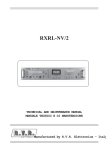
1
TEX LCD
User Manual
Manufactured by
Italy
File name:
TEXLCD_EN.P65
Version:
1.1
Date:
06/09/2002
Revision History
Version
Date
Reason
Editor
1.0
18/01/2002
New version
D. Canazza
1.1
06/09/2002
Add telemetry board
J. Berti
TEX LCD - User Manual
Version 1.1
© Copyright 2002
R.V.R. Elettronica SpA
Via del Fonditore 2/2c - 40138 - Bologna (Italia)
Telefono:
+39 051 6010506
Fax:
+39 051 6011104
Email:
[email protected]
Web:
www.rvr.it
All rights reserved
Printed and bound in Italy. No part of this manual may be reproduced,
memorized or transmitted in any form or by any means, electronic or
mechanic, including photocopying, recording or by any information
storage and retrieval system, without written permission of the copyright
owner.
Notification of intended purpose and limitations of product use
This product is a FM transmitter intended for FM audio broadcasting. It utilises
operating frequencies not harmonised in the intended countries of use.
The user must obtain a license before using the product in intended country of
use. Ensure respective country licensing requirements are complied with.
Limitations of use can apply in respect of operating freuency, transmitter power
and/or channel spacing.
Declaration of Conformity
Hereby, R.V.R. Elettronica SpA, declares that this FM transmitter is in
compliance with the essential requirements and other relevant provisions of
Directive 1999/5/EC.
This page intentionally left blank
TEX LCD
Table of Contents
1.
2.
3.
3.1
3.2
4.
5.
5.1
5.2
5.3
5.4
6
6.1
6.2
6.3
6.4
6.5
6.6
6.7
7.
7.1
7.2
8.
8.1
8.2
8.3
8.4
8.5
9.
9.1
9.2
Preliminary Instructions
Warranty
First Aid
Treatment of electrical shocks
Treatment of electrical Burns
General Description
Quick guide for installation and use
Preparation
Use
Settings and calibration
Software
External Description
Front Panel
Rear Pannel (MONO version with telemetry)
Rear Pannel (STEREO version with telemetry)
Connectors description
Rear Pannel (Mono version)
Rear Pannel (Stereo version)
Connectors description
Technical specifications
Physical specifications
Electrical specifications
Working Principles
Power Supply
Panel board
Main board
Power amplifier
Telemetry board
Identification and Access to the Modules
Identification of the Modules
Removing the Modules
Appendix:
Component layouts, schematics, bills of material
User Manual
Rev. 1.1 - 06/09/02
1
2
4
4
5
7
9
9
9
10
11
17
17
18
19
20
21
22
23
25
25
25
27
28
28
29
30
30
31
31
32
i
TEX LCD
This page was intentionally left blank
ii
Rev. 1.1 - 06/09/02
User Manual
TEX LCD
1. Preliminary Instructions
This manual is written as a general guide for those having previous knowledge
and experience with this kind of equipment, well conscious of the risks connected
with the operation of electrical equipment.
It is not intended to contain a complete statement of all safety rules which should
be observed by personnel in using this or other electronic equipment.
The installation, use and maintenance of this piece of equipment involve risks
both for the personnel performing them and for the device itself, that shall be used
only by trained personnel.
R.V.R. Elettronica SpA doesn’t assume responsibility for injury or damage resulting
from improper procedures or practices by untrained/unqualified personnel in the
handling of this unit.
Please observe all local codes and fire protection standards in the operations of
this unit.
WARNING: always disconnect power before opening covers or removing any
part of this unit.
Use appropriate grounding procedures to short out capacitors and high voltage
points before servicing.
WARNING: this device can irradiate radio frequency waves, and if it’s not installed
following the instructions contained in the manual and local regulations it could
generate interferences in radio communications.
This is a "CLASS A" equipment. In a residential place this equipment can cause
hash. In this case can be requested to user to take the necessary measures.
R.V.R. Elettronica SpA reserves the right to modify the design and/or the technical
specifications of the product and this manual without notice.
User Manual
Rev. 1.1 - 06/09/02
1 / 32
TEX LCD
2. Warranty
Any product of R.V.R. Elettronica is covered by a 24 (twenty-four) month warranty.
For components like tubes for power amplifiers, the original manufacturer’s warranty
applies.
R.V.R. Elettronica SpA extends to the original end-user purchaser all
manufacturers warranties which are transferrable and all claims are to be made
directly to R.V.R. per indicated procedures.
Warranty shall not include:
1 danni verificatisi durante la spedizione della macchina alla R.V.R. per eventuali
riparazioni;
2 Any unauthorized repair/modification;
3 Incidental/consequential damages as a result of any defect
4 Nominal non-incidental defects
5 Re-shipment costs or insurance of the unit or replacement units/parts
Any damage to the goods must be reported to the carrier in writing on the shipment
receipt.
Any discrepancy or damage discovered subsequent to delivery, shall be reported
to R.V.R. Elettronica within 5 (five) days from delivery date.
To claim your rights under this warranty, you shold follow this procedure:
1 Contact the dealer or distributor where you purchased the unit. Describe the
problem and, so that a possible easy solution can be detected.
Dealers and Distributors are supplied with all the information about problems
that may occur and usually they can repair the unit quicker than what the
manufacturer could do. Very often installing errors are discovered by dealers.
2 If your dealer cannot help you, contact R.V.R. Elettronica and explain the
problem. If it is decided to return the unit to the factory, R.V.R. Elettronica
will mail you a regular authorization with all the necessary instructions to send
back the goods.
3 When you receive the authorization, you can return the unit. Pack it carefully
for the shipment, preferably using the original packing and seal the package
perfectly. The customer always assumes the risks of loss (i.e., R.V.R. is never
responsible for damage or loss), until the package reaches R.V.R. premises.
For this reason, we suggest you to insure the goods for the whole value.
Shipment must be effected C.I.F. (PREPAID) to the address specified by R.V.R.’s
service manager on the authorization
DO NOT RETURN UNITS WITHOUT OUR AUTHORIZATION AS THEY WILL
BE REFUSED
2 / 32
Rev. 1.1 - 06/09/02
User Manual
TEX LCD
4 Be sure to enclose a written technical report where mention all the problems
found and a copy of your original invoice establishing the starting date of the
warranty.
Replacement and warranty parts may be ordered from the following address. Be
sure to include the equipment model and serial number as well as part description
and part number.
R.V.R. Elettronica SpA
Via del Fonditore, 2/2c
40138 BOLOGNA
ITALY
Tel. +39 051 6010506
User Manual
Rev. 1.1 - 06/09/02
3 / 32
TEX LCD
3. First Aid
The personnel employed in the installation, use and maintenance of the device,
shall be familiar with theory and practice of first aid..
3.1
3.1.1
Treatment of electrical shocks
If the victim is not responsive
Follow the A-B-C's of basic life support
•
Place victim flat on his backon a hard surface.
•
Open airway: lift up neck, push forehead back (Fig. 3-1).
•
clear out mouth if necessary and observe for breathing
•
if not breathing, begin artificial breathing (Figure 3-2): tilt head, pinch nostrils,
make airtight seal, four quick full breaths. Remember mouth to mouth
resuscitation must be commenced as soon as possible
Figure 3-1
•
Check carotid pulse (Fig 3-3); if pulse is absent, begin artificial circulation
(Fig. 3-4) depressing sternum (Fig. 3-5)
Figure 3-3
4 / 32
Figure 3-2
Figure 3-4
Figure 3-5
•
In case of only one rescuer, 15 compressions alternated to two breaths.
•
If there are two rescuers, the rythm shall be of one brath each 5 compressions.
•
Do not interrupt the rythm of compressions when the second person is giving
breath.
•
Call for medical assistance as soon as possible.
Rev. 1.1 - 06/09/02
User Manual
TEX LCD
3.1.2
3.2
3.2.1
If victim is responsive
•
Keep them warm
•
Keep them as quiet as possible
•
Loosen their clothing (a reclining position is recommended)
•
Call for medical help as soon as possible
Treatment of electrical Burns
Extensive burned and broken skin
•
Cover area with clean sheet or cloth
•
Do not break blisters, remove tissue, remove adhered particles of clothing, or
apply any salve or ointment.
•
Treat victim for shock as required.
•
Arrange transportation to a hospital as quickly as possible.
•
If arms or legs are affected keep them elevated
If medical help will not be available within an hour and the victim is conscious and
not vomiting, give him a weak solution of salt and soda: 1 level teaspoonful of salt
and 1/2 level teaspoonful of baking soda to each quart of water (neither hot or
cold). Allow victim to sip slowly about 4 ounces (half a glass) over a period of 15
minutes. Discontinue fluid if vomiting occurs
DO NOT give alcohol
3.2.2
Less severe burns
•
Apply cool (not ice cold) compresses using the cleansed available cloth article.
•
Do not break blisters, remove tissue, remove adhered particles of clothing, or
apply salve or ointment.
•
Apply clean dry dressing if necessary.
•
Treat victim for shock as required.
•
Arrange transportation to a hospital as quickly as possible
•
If arms or legs are affected keep them elevated.
User Manual
Rev. 1.1 - 06/09/02
5 / 32
TEX LCD
This page was intentionally left blank
6 / 32
Rev. 1.1 - 06/09/02
User Manual
TEX LCD
4. General Description
The TEX LCD is an exciter for Frequency Modulated audio broadcasting in a
frequency modulation able to transmit in the band between 87.5 and 108 MHz
with an output RF power adjustable up to a maximum of 30 W
Outstanding audio features this device has are low distortion and intermodulation
values (typically 0.03%) and the high signal to noise ratio (typically 80 dB). Another
important feature the TEX LCD has is its great simplicity of construction and use.
For example, the mains power supply is universal type and allows any voltage
between 90 V and 260 V to be used without having to select it manually.
The TEX LCD was designed to be modular. Its various functions are run from
modules directly connected to each other with male and female connectors or
with flat cables ending in connectors. This type of design makes maintenance
operations and any required module replacement easier. All models are made
with SMD technology.
This exciter contains a low-pass filter that reduces the harmonic emissions to
below the limits allowed by international regulations, and can therefore be used
as a transmitter connected directly to the antenna.
The machine is offered in two versions, one for Mono or MPX input (wideband
input that is useful when you want to transmit in stereo using an external stereo
encoder) and the other with an integrated stereo encoder. The TEX LCD stereo
encoder guarantees excellent stereo separation together with a low harmonic
distortion level. Also the stereo version of the exciter can be configured for operating
in Mono/MPX mode (meaning excluding the stereophonic coder and using the
"left" input as the "mono" input and the BNC as the "MPX").
The user can do the configuration through microswitches that are accessible from
the outside.
Both versions have two inputs (SCA1 and SCA2) for modulated signals on
subcarriers from special external encoders normally used in Europe for RDS (Radio
Data System) transmission.
This exciter contains two types of control circuits, the "analogue" type made as
hardware inside the power amplifier and the "digital" type made by the management
software on a microcontroller. The analogue control maintains the RF output power
at a constant level and limits it in case there is an excess of stationary waves.
The microprocessor system includes an LCD display and push-button panel for
interaction with the user, and implements the following functions:
•
Setting the output power
•
Setting the operating frequency
•
Activation and deactivation of power delivery
•
Measurement and display of the working parameters of the exciter
•
Communications with outside devices
User Manual
Rev. 1.1 - 06/09/02
7 / 32
TEX LCD
The exciter's management software is based on a menu system. The user can
navigate between the various submenus by using four push buttons: ESC, LEFT/
UP, RIGHT/DOWN and ENTER.
Four LEDs indicate the machine status and are found on the front panel: ON,
LOCK, FOLDBACK and RF MUTE.
The exciter has one input for external 24 VDC power supply. This source of auxiliary
power supply, which the user can make through buffer batteries, is used
automatically in the case of mains voltage failure.
8 / 32
Rev. 1.1 - 06/09/02
User Manual
TEX LCD
5. Quick guide for installation and use
This chapter contains the necessary information for installing and using the
machine. In the event any aspects are not completely clear, for example when
using the machine for the first time, we recommend you carefully read the entire
description contained in this manual.
5.1
Preparation
Unpack the exciter and before doing any other operation, be sure it has not been
damaged during transport. In particular check that all the connectors are in perfect
condition.
The main fuse can be accessed from the outside on the rear panel (see figures
6.2 and 6.3). Extract the fuse carrier with a screwdriver to check its integrity or for
replacement, if necessary. The fuse to be used is this type:
3.15 A
5X20
Check that the TEX LCD switches are in the "off" position. The exciter has two
switches: one is incorporated in the VDE base for the mains power supply cable
and completely interrupts the machine's mains power supply, whereas the second
one is on the front panel and inhibits the switching power supply of the machine.
Connect the RF output of the exciter to the antenna cable or to a fictitious load
able to dissipate the power generated by the TEX LCD.
Connect the mains cable to the special VDE base.
NOTE: It is crucial that the mains system be provided with earthing to ensure both
the operators' safety and correct operation of the device.
Connect the audio cables of the signal source to the proper connectors on the
back of the exciter.
5.2
Use
Energize the exciter by putting the switch found on the rear panel in the "I" position
(on) and turn it on with the switch found on the front panel.
Enter the "Set" menu and set the desired operating frequency. See chapter 5.4 for
a description of the various menus..
By using the switches and trimmer found on the rear panel, set the characteristics
(impedance, preemphasis and, if it’s necessary, stereo/mono) and the levels of
the audio and RDS inputs (if used).
User Manual
Rev. 1.1 - 06/09/02
9 / 32
TEX LCD
NOTE: When the device leaves the factory, it is delivery with the output power
adjustment at minimum and in the OFF position. It is however recommended that
you always check the set level before activating power supply, especially if the
machine is used as a modulator for a power amplifier.
Set the desired power level from the predefined menu.
Activate the RF power output from the "Fnc" menu.
5.3
Settings and calibration
The only adjustments to be manually made on the TEX LCD are those relating to
the audio operation levels and modes..
A trimmer for each one of the exciter's inputs is on the rear panel of the device.
The printing on the panel indicates which input each trimmer refers to. The
sensitivity of the various inputs can be adjusted using the trimmers within the
limits described in the following tables:
•
Input sensitivity - mono version
Input
RDS
SCA1
SCA2
MPX
Mono
•
Figure 6.2
[5]
[4]
[16]
[20]
[8]
Trimmer
[6]
[18]
[17]
[19]
[7]
Sensitivity
-20 ÷ +13 dBm
- 8 ÷ +13 dBm
- 8 ÷ +13 dBm
-13 ÷ +13 dBm
-13 ÷ +13 dBm
Notes
Input level for 2.0 kHz deviation
Input level for 7.5 kHz deviation
Input level for 75 kHz deviation
Input sensitivity - stereo version
Input
RDS
SCA1
SCA2
Left
Right
Figure 6.3
[8]
[7]
[19]
[23]
[11]
Trimmer
[9]
[21]
[20]
[22]
[10]
Sensitivity
-20 ÷ +13 dBm
- 8 ÷ +13 dBm
- 8 ÷ +13 dBm
-13 ÷ +13 dBm
-13 ÷ +13 dBm
Notes
Input level for 2.0 kHz deviation
Input level for 7.5 kHz deviation
Input level for 75 kHz overall deviation
(i.e. comprising channels + pilot tone)
When adjusting the sensitivity level of the inputs, keep in mind that the
instantaneous modulation level is given in the predefined menu and that an indicator
signals the 75 kHz level. To get a proper adjustment, we recommend you put a
level signal on the machine's output equivalent to the level of its own audio program
and adjust the relative trimmer until the instantaneous deviation coincides with
the indication of 75 kHz.
To adjust the levels of the inputs of the subcarriers, you can use a similar procedure
while getting help from the "X10" option that can be selected from the Fnc menu.
With this option, the modulation level indicated is multiplied by a factor 10 so the
drawn indication of the predefined menu coincides with a deviation value of 7.5
kHz.
10 / 32
Rev. 1.1 - 06/09/02
User Manual
TEX LCD
For the stereophonic version, there is a special menu in which the levels of the
Right and Left channels are indicated separately with the relative indicators of the
nominal levels for the maximum deviation of 75 kHz.
The positions of the DIP switches that are used to select the available options are
indicated on the printing.
Mono version preemphasis (switch [17] Figure 6.2):
•
ON
1
ON
50 µs
2
1
2
75 µs
Mono version impedances of input (switch [23] Figure 6.2):
•
1
ON
Switch 1: XLR input impedance, ON = 600 Ω, OFF = 10 kΩ
2
Switch 2: BNC input impedance, ON = 50 Ω, OFF = 10 kΩ
Stereo version preemphasis (switch [7] Figure 6.3):
•
ON
1
ON
2
3
4
50 µs
1
2
3
4
75 µs
L and R input impedance (type XLR) (switch [25] Figure 6.3):
•
ON
1
Switch 1: R XLR input impedance, ON = 600 Ω, OFF = 10 kΩ
2
Switch 2: L XLR input impedance, ON = 600 Ω, OFF = 10 kΩ
Operation mode/input impedance MPX ([8] Figure 6.3)
(switch [6] Figure 6.2):
•
ON
1
Switch 1: Operation mode ON = Mono, OFF = Stereo
2
Switch 2: MPX input impedance, ON = 50 Ω, OFF = 10 kΩ
5.4
Software
The machine is provided with a two-line LCD display where a set of menus is
shown. An overall view of the machine's menus is given in figure 5-1.
One of the following symbols may be present on the left side of the display,
depending on the case:
The parameter highlighted by the arrow can be modified
The arrow points out the current line, the parameter of which cannot be modified.
This symbol is present in the menus made up of more than two lines to help
scroll the menu.
User Manual
Rev. 1.1 - 06/09/02
11 / 32
TEX LCD
When turned on, the LCD display shows the predefined screen with the graphic
representation of the instantaneous modulation level and indication of the direct
power supplied:
The vertical bars under "Mod" indicate the progress of the modulation in real time;
the hatched bar signals the maximum nominal modulation level of 75 kHz (100%).
To change the set power level, select the line relating to the power with the DOWN
push button and keep the ENTER push button pressed until it enters the
modification mode. The screen that is shown in the modification mode is similar to
the following:
The bottom line gives the instantaneous reading of the power (30W in this example),
whereas the bar indicates the set level. To increase the level, press the RIGHT/
DOWN push button and to reduce it, press LEFT/UP. As the set level increases or
decreases, the bar becomes longer or shorter to display the current setting. When
the desired level is reached, press ENTER to confirm and exit the predefined
menu. Note that the set value is stored anyway, so if you press ESC or let the
timeout go by without pressing a key, the power will remain at the last set level.
If you press the ESC push button while you are in the predefined menu, you will
be shown the following selection screen from which you can access all the other
menus:
To enter one of the submenus, select its name (which will be underlined by a
blinking cursor) with the RIGHT or LEFT push buttons and then press the ENTER
push button.
If you instead want to go back to the predefined menu, all you have to do is press
the ESC push button again..
Figure 5.1 shows the complete set of the machine's menus.
NOTE: The "L&R" menu is active only in the stereo version. The writing "L&R"
appear in the selection menu of the mono version, but doesn’t have any meaning.
12 / 32
Rev. 1.1 - 06/09/02
User Manual
TEX LCD
Switch on
ESC
ESC
Selection Menu
ENTER
Operation Menu (Fnc)
ENTER
Power Menu (Pwr)
ENTER
ENTER
ENTER
Power Amp Menu (P.A)
Setting Menu (Set)
Miscellaneous Menu (Mix)
ENTER
Version Menu (Vrs)
ENTER
Channels Menu (L&R)
Figure 5.1
5.4.1
Operation Menu (Fnc)
The user can set the deviation display mode and activate or deactivate the supply
of power from the exciter from this menu.
To work with one of the two functions, select the relative line with the UP and
DOWN push buttons and then press and continue pressing the ENTER push button
until the command is accepted. This was the Pwr setting will go from On to Off or
vice versa and the Mod setting will go from "X1" to "X10" or vice versa.
The indication of the instantaneous deviation is multiplied by a factor 10 in the
"X10" mode, so the hatched indicator on the predefined menu will coincide with
the 7.5 kHz value instead of 75 kHz. This display mode is useful when you want
to view low deviation levels such as, for example, those due to the pilot tone or to
the subcarriers.
5.4.2
Power Menu (Pwr)
This screen shows the user the measures relating to the exciter’s RF power output:
User Manual
Rev. 1.1 - 06/09/02
13 / 32
TEX LCD
•
Forward Power (Fwd )
•
Reflected Power (Rfl)
The values shown are "readings", and therefore cannot be modified (note the
empty triangle). To modify the power setting, use the predefined menu as described
above.
5.4.3
Power Amplifier Menu (P.A)
This screen, consisting of three lines that can be scrolled with the UP and DOWN
push buttons, shows the user the measures relating to the device's final power
amplifier:
5.4.4
•
Voltage (VPA)
•
Current consumption (IPA)
•
Temperature (TMP)
Settings Menu (Set)
This menu lets you read and set the operating frequency.
By pressing the ENTER push button, you can modify the set frequency using the
UP (the frequency increases) and DOWN push buttons.
After having set a new frequency value, press the ENTER push button to confirm
the choice. The exciter will release from the current frequency (the LOCK LED
turns off) and it will latch onto the new operating frequency (LOCK turns back on).
Instead, if you press ESC or let the timeout go by, the frequency will remain set at
the previous value.
5.4.5
Miscellaneous Menu (Mix)
This menu allows you to set the machine's address in a o I2C type of serial bus
connection:
14 / 32
Rev. 1.1 - 06/09/02
User Manual
TEX LCD
The I2C network address is important when the exciter is connected to an RVR
transmission system that envisages use of this protocol. We recommend you do
not modify it without a good reason.
5.4.6
Versions Menu(Vrs)
This screen shows the version and the release date of the software.
5.4.7
Channels Menu (L&R)
This menu is active in the stereo version of the machine and in the mono version,
but in the mono version the menu doesn’t have any meaning.
The right and left channel input levels are depicted with vertical bars, as shown in
the following figure.
The hatched bar indicates the level that corresponds with the total deviation at
100%, and is useful to regulate the input levels of the audio channels.
Please note that if you set a stereo TEX-LCD exciter for mono operation, this
menu is still active, and it will only show the level of the mono input.
Please remember that the modulation level is always shown by the default menu.
User Manual
Rev. 1.1 - 06/09/02
15 / 32
TEX LCD
This page was intentionally left blank
16 / 32
Rev. 1.1 - 06/09/02
User Manual
TEX LCD
6 External Description
This chapter reports the elements of the front and rear panels of the TEX-LCD
with a brief description of each of them.
6.1
Front Panel
Figure 6.1
[1]
[2]
[3]
[4]
AIR FLOW
ON
LOCK
FOLDBACK
[5] R.F. MUTE
[6] CONTRAST
[7] ESC
[8] LEFT/UP
[9] RIGHT/DOWN
[10] ENTER
[11] DISPLAY
[12] POWER
User Manual
Grid for the intake of the air flow of the forced ventilation
Green LED, lit when the exciter is working
Green led, lit when the PLL is locked on the working frequency
Yellow LED, lit when the foldback function is operating
(automatic reduction of the delivered RF power)
Yellow LED, lit when the exciter’s power output is inhibited by an
external interlock command
Display contrast adjusting trimmer
Push button to exit from a menu
Push button to move in the menu system and to modify the
parameters
Push button to move in the menu system and to modify the
parameters
Push button to confirm a parameter and to enter in a menu
Liquid crystals display
ON/OFF switch. This switch disables the exciter without
disconnecting the mains supply
Rev. 1.1 - 06/09/02
17 / 32
TEX LCD
6.2
Rear Pannel (MONO version with telemetry)
Figure 6.2
[1] FUSE
[2] R.F. OUTPUT
[3] INTERLOCK
[4] FWD EXT. AGC
[5] RFL EXT. AGC
[6]
[7]
[8]
[9]
[10]
[11]
[12]
[13]
[14]
[15]
[16]
SCA 1
MPX/RDS
MPX/RDS ADJ
RIGHT/MONO ADJ
RIGHT/MONO
PLUG
24 VDC IN
FAN
R.F. TEST POINT
REMOTE
RS232
[17] PREENPHASIS
[18]
[19]
[20]
[21]
[22]
[23]
18 / 32
SCA 2
SCA2 ADJ
SCA1 ADJ
LEFT-MONO/MPX ADJ
LEFT-MONO/MPX
IMPEDANCE
Fuse holder. Use a screwdriver to access the fuse
Contains the general protection fuse rated 3.15 A
RF output connector, N-type, 50Ω.
BNC interlock connector: the exciter is forced in stand-by mode
when the inner conductor is grounded.
Trimmer for the control of the delivered power in function of the
income FWD fold (see cap. 6.4.2)
Trimmer for the control of the delivered power in function of the
income RFL fold (see cap. 6.4.2)
BNC connector, SCA1 unbalanced input
BNC connector, MPX unbalanced input
Adjustment trimmer for MPX input
Adjustment trimmer for the Mono input
XLR connector for balanced Mono audio input
Mains supply plug, 90 - 260V 50-60 Hz
External 24Vdc supply input. Positive (red) and negative (black)
Fan for the forced ventilation of the exciter
RF test output, approx. -30 dB wrt the RF output power level
DB9 connector for telemetry of the machine
DB9 connector for interconnection with other devices and for
factory parameters programming
Dip-switch to set the preenphasys at 50 or 75 µs. The
preenphasys setting is only relevant for the mono input, while
MPX input is unaffected by this setting
BNC connector, SCA2 unbalanced input
Adjustment trimmer for SCA2 input
Adjustment trimmer for SCA1 input
Adjustment trimmer for MPX input
BNC connector, MPX unbalanced input
Dip-switch to set the input impedance
600Ω or 10kΩ for the mono input
50Ω or 10kΩ for the MPX input
Rev. 1.1 - 06/09/02
User Manual
TEX LCD
6.3
Rear Pannel (STEREO version with telemetry)
figure 6.3
[1] FUSE
[2] R.F. OUTPUT
[3] INTERLOCK
[4] FWD EXT. AGC
[5] RFL EXT. AGC
[6] PHASE ADJ
[7] PREENPHASIS
[8] MODE/MPX IMP
[9]
[10]
[11]
[12]
[13]
[14]
[15]
[16]
[17]
[18]
[19]
SCA 1
MPX/RDS
MPX/RDS ADJ
RIGHT/MONO ADJ
RIGHT/MONO
PLUG
24VDC IN
FAN
R.F. TEST POINT
REMOTE
RS232
[20] 19 KHZ PILOT
[21]
[22]
[23]
[24]
[25]
[26]
SCA 2
SCA2 ADJ
SCA1 ADJ
LEFT-MONO/MPX ADJ
LEFT-MONO/MPX
IMPEDANCE
User Manual
Fuse holder. Use a screwdriver to access the fuse
Contains the general protection fuse rated 3.15 A
RF output connector, N-type, 50Ω.
BNC interlock connector: the exciter is forced in stand-by mode
when the inner conductor is grounded.
Trimmer for the control of the delivered power in function of the
income FWD fold (see cap. 6.4.2)
Trimmer for the control of the delivered power in function of the
income RFL fold (see cap. 6.4.2)
Pilot tone phase adjustment trimmer
Dip-switch to set the preenphasys at 50 or 75 µs. The
preenphasys setting is only relevant for the Left and Right
inputs in stereo mode and for the mono input in mono mode,
while MPX input is unaffected by this setting
Dip-switch to set the operation mode (STEREO or MONO) and
the MPX input impedance, 50Ω or 10kΩ.
BNC connector, SCA1 unbalanced input
BNC connector, MPX unbalanced input
Adjustment trimmer for MPX input
Adjustment trimmer for the Right channel input
XLR connector, balanced Right channel input
Mains supply plug, 90 - 260V 50-60 Hz
External 24Vdc supply input. Positive (red) and negative (black)
Fan for the forced ventilation of the exciter
RF test output, approx. -30 dB wrt the RF output power level
DB9 connector for telemetry of the machine
DB9 connector for interconnection with other devices and for
factory parameters programming
BNC output for the 19 kHz pilot tone. This can be used for
external devices (e.g. RDS coders) synchronization
BNC connector, SCA2 unbalanced input
Adjustment trimmer for SCA2 input
Adjustment trimmer for SCA1 input
Adjustment trimmer for Left-Mono channel input
XLR connector, balanced Left-Mono channel input
Dip-switch to set the balanced input impedance,
600Ω or 10kΩ
Rev. 1.1 - 06/09/02
19 / 32
TEX LCD
6.4
Connectors description
6.4.1
RS232
Type: DB9 female
1
6
1
2
3
4
5
6
7
8
9
NC
TX_D
RX_D
Internally connected with 6
GND
Internally connected with 4
Internally connected with 8
Internally connected with 7
NC
Note: pins 6, 7 and 8 are for factory programming and should not be connected
6.4.2
Remote
Type: DB15 female
1
9
6.4.3
1
2
3
4
5
6
7
8
9
10
11
12
13
14
15
Interlock
FWD fold
GND
SDA IIC Bus
VPA Tlm
FWD tlm
Power Good
GND
GND
RFL fold
SCL IIC Bus
IPA Tlm
RFL Tlm
On cmd
OFF cmd
Left (MONO) / Right (MPX)
Type: XLR female
2
1
3
20 / 32
1
2
3
GND
Positive
Negative
Rev. 1.1 - 06/09/02
User Manual
TEX LCD
6.5
Rear Pannel (Mono version)
Figure 6.5
[1] FUSE
[2] R.F. OUTPUT
[3] INTERLOCK
[4]
[5]
[6]
[7]
[8]
[9]
[10]
[11]
[12]
[13]
[14]
[15]
SCA 1
MPX/RDS
MPX/RDS ADJ
RIGHT/MPX ADJ
RIGHT/MPX
PLUG
24 VDC IN
FAN
R.F. TEST POINT
REMOTE
RS232/I2C BUS
PREENPHASIS
[16]
[17]
[18]
[19]
[20]
[21]
SCA 2
SCA2 ADJ
SCA1 ADJ
LEFT-MONO/MPX ADJ
LEFT-MONO/MPX
IMPEDANCE
User Manual
Fuse holder. Use a screwdriver to access the fuse
Contains the general protection fuse rated 3.15 A
RF output connector, N-type, 50Ω.
BNC interlockconnector: the exciter is forced in stand-by mode
when the inner conductor is grounded.
BNC connector, SCA1 unbalanced input
BNC connector, MPX unbalanced input
Adjustment trimmer for MPX input
Adjustment trimmer for the Mono input
XLR connector for balanced mono audio input
Mains supply plug, 90 - 260V 50-60 Hz
External 24Vdc supply input. Positive (red) and negative (black)
Fan for the forced ventilation of the exciter
RF test output, approx. -30 dB wrt the RF output power level
DB9 connector for serial communications and via modem
DB9 connector for I2C standard communication
Dip-switch to set the preenphasys at 50 or 75 µs. The
preenphasys setting is only relevant for the mono input, while
MPX input is unaffected by this setting
BNC connector, SCA2 unbalanced input
Adjustment trimmer for SCA2 input
Adjustment trimmer for SCA1 input
Adjustment trimmer for MPX input
BNC connector, MPX unbalanced input
Dip-switch to set the input impedance
600Ω or 10kΩ for the mono input
50Ω or 10kΩ for the MPX input
Rev. 1.1 - 06/09/02
21 / 32
TEX LCD
6.6
Rear Pannel (Stereo version)
figure 6.6
[1] FUSE BLOCK
[2] R.F. OUTPUT
[3] INTERLOCK
[4] PHASE ADJ
[5] PREENPHASIS
[6] MODE/MPX IMP
22 / 32
[7]
[8]
[9]
[10]
[11]
[12]
[13]
[14]
[15]
[16]
[17]
[18]
SCA 1
MPX/RDS
MPX/RDS ADJ
RIGHT/MPX ADJ
RIGHT/MPX
PLUG
24VDC IN
FAN
R.F. TEST POINT
REMOTE
RS232/I2C BUS
19 KHZ PILOT
[19]
[20]
[21]
[22]
[23]
[24]
SCA 2
SCA2 ADJ
SCA1 ADJ
LEFT-MONO/MPX ADJ
LEFT-MONO/MPX
IMPEDANCE
Fuse holder. Use a screwdriver to access the fuse
Contains the general protection fuse rated 3.15 A
RF output connector, N-type, 50Ω.
BNC interlockconnector: the exciter is forced in stand-by mode
when the inner conductor is grounded.
Pilot tone phase adjustment trimmer
Dip-switch to set the preenphasys at 50 or 75 µs. The
preenphasys setting is only relevant for the Left and Right
inputs in stereo mode and for the mono input in mono mode,
while MPX input is unaffected by this setting
Dip-switch to set the operation mode (STEREO or MONO) and
the MPX input impedance, 50Ω or 10kΩ.
BNC connector, SCA1 unbalanced input
BNC connector, MPX unbalanced input
Adjustment trimmer for MPX input
Adjustment trimmer for the Right channel input
XLR connector, balanced Right channel input
Mains supply plug, 90 - 260V 50-60 Hz
External 24Vdc supply input. Positive (red) and negative (black)
Fan for the forced ventilation of the exciter
RF test output, approx. -30 dB wrt the RF output power level
DB9 connector for serial communications and via modem
DB9 connector for I2C standard communiaction
BNC output for the 19 kHz pilot tone. This can be used for
external devices (e.g. RDS coders) synchronization
BNC connector, SCA2 unbalanced input
Adjustment trimmer for SCA2 input
Adjustment trimmer for SCA1 input
Adjustment trimmer for Left/Mono channel input
XLR connector, balanced Left/Mono channel input
Dip-switch to set the balanced input impedance,
600Ω or 10kΩ
Rev. 1.1 - 06/09/02
User Manual
TEX LCD
6.7
6.7.1
Connectors description
RS232 / I2C Bus (USED ONLY FOR PROGRAMMATION)
Type: DB9 female
1
6.7.2
6
1
2
3
4
5
6
7
8
9
GND
SDA
SCL
NC
GND
Internally used (NOT CONNECTED)
Internally used (NOT CONNECTED)
Internally used (NOT CONNECTED)
GND
Remote (USED FOR RS232 COMMUNICATION)
Type: DB9 female
1
6.7.3
6
1
2
3
4
5
6
7
8
9
NC
TX_D
RX_D
Internally connected with 6
GND
Internally connected with 4
Internally connected with 8
Internally connected with 7
NC
Left (MONO) / Right (MPX)
Type: XLR female
2
1
3
User Manual
1
2
3
GND
Positive
Negative
Rev. 1.1 - 06/09/02
23 / 32
TEX LCD
This page was intentionally left blank
24 / 32
Rev. 1.1 - 06/09/02
User Manual
TEX LCD
7. Technical specifications
7.1
Physical specifications
Panel size
Depth
Weight
Working Temperature
7.2
483 mm (19”) x 88 mm (3 1/2”) (2 HE)
344 mm (26 1/2”)
Circa 6 Kg
-10 °C ÷ 50 °C
Electrical specifications
General
RF output power
RF output connector
RF output impedance
Frequency range
Frequency setting
Frequency stability
Modulation type
Spurious and Harmonics suppression
Modulation capability
Asyncronous residual AM
Syncronous residual AM
C.A. power supply
C.C. power supply
Power consumption
0 to 30 W, adjustable
"N"-type
50 Ohm
87.5 MHz ÷ 108 MHz
Direct software programming
±1ppm from -10°C to 50°C
Direct carrier modulation
Respects relevant FCC and CCIR standards
(typical -75 dBc)
Respects relevant FCC and CCIR standards
(typical 240khz MPX/Mono, 210 KHz Stereo)
< -70 dB wrt. 100% peak AM
< -50 dB wrt. 100% peak AM, with 75 kHz
deviation @ 400Hz
≅ 80 V ÷ 260 V, full-range
24 V
120 VA ca.
Input
Left, Right and Mono Input
Type: XLR female
balanced or unbalanced
MPX input
Type: BNC, unbalanced
Input impedance
balanced input: 600 or 10 k Ohm selectable
unbalanced input: 50 or 10 k Ohm selectable
Input level
-13 dBm ÷ +13 dBm, continuosly adjustable
Preemphasys
Selectable:
0
50 us (CCIR)
75 us (FCC)
SCA/RDS input
3 BNC unbal (2 in the stereo version)
SCA/RDS input impedance
10 kOhm
SCA/RDS input level
-20 dBm ÷ +13 dBm for 2.0 kHz
continuosly adjustable
SCA/RDS amplitude/frequency response ± 0.2 dB, 40 kHz to 100 kHz
Output
RF Out:
RF Test
19 kHz pilot tone output
User Manual
“N”-type, 50 Ohm
BNC connector, -30 dB wrt. carrier level
50 Ohm
BNC connector, 1 Vpp
minimum load 4.7 kOhm
Rev. 1.1 - 06/09/02
25 / 32
TEX LCD
MONO operation
S/N
Amplitude frequency response
Total harmonic distortion (THD)
> 80dB wrt. 75 kHz, measured in the band
20 Hz ÷ 20 kHz, 50 us deemph., RMS detect
± 0.5 dB, 20Hz ÷ 15Khz
< 0.05%
MPX operation
composite S/N
MPX amplitude frequency response
MPX Total harmonic distortion (THD)
Stereo separation
> 80dB wrt. 75 kHz, measured in the band
20 Hz ÷ 20 kHz, 50 us deemph., RMS detect
± 0.05 dB, 20 Hz ÷ 53 KHz
± 0.2 dB, 53 KHz ÷ 100 KHz
< 0.02 %
> 55 dB (typ. 60dB, with external stereo
coder)
Stereo operation
S/N FM Stereo
Risposta ampiezza/frequenza audio
Total harmonic distortion (THD)
Stereo separation
> 74 dB wrt. 75 kHz, measured on decoded
channels, in the band 20 Hz ÷ 20 KHz,
50 us deemph, RMS detector
± 0.5 dB, 20 Hz ÷ 15 KHz
≤ 0.05 %
> 50 dB
Connections
Interlock connector
Serial interface
Remote
26 / 32
BNC, inhibits RF power output when shorted
DB9 female RS232
DB15 female, give indications on the state of
the device
Rev. 1.1 - 06/09/02
User Manual
TEX LCD
8. Working Principles
A schematic view of the modules and connections making up the TEX-LCD with
the telemetry board is shown in figure 8.1.
PANEL
CARD
2
4
6
8
10
12
14
16
JP5
CN16PD
PA
1
3
5
7
9
11
13
15
2
4
6
8
10
12
14
16
JP5
CN16PD
IIC
1
3
5
7
9
11
13
15
2
4
6
8
10
12
14
16
JP6
CN16PD
PS
1
3
5
7
9
11
13
15
1
3
5
7
9
11
13
15
2
4
6
8
10
12
14
16
2
4
6
8
10
1
3
5
7
9
JP3
CN10PD
RS232
2
JP4
MAIN
CN16PD
16
14
12
10
8
6
4
2
15
13
11
9
7
5
3
1
1
9
2
10
3
11
4
12
5
13
6
14
7
15
8
1
FAN1
8414 NGH
JP5
CN2
CN16PD
PA
P1
BNC
1
3
5
7
9
11
13
15
2
1
2
4
6
8
10
12
14
16
DB15
JP2
2.5MSF
1
J2
FLAT-16A
1
TELEMETRY CARD
POWER
AMPLIFIER
JP1
CN16PD
1
3
5
7
9
11
13
15
1
2
4
6
8
10
12
14
16
J1
FAST ON
2
5
3
4
CN1
SMB_CS
A
POWER SUPPLY
STEREO/MONO CARD
JP3
1
2
2.5MSF
D1
DIODE
1
6
2
7
3
8
4
9
5
1
9
2
10
3
11
4
12
5
13
6
14
7
15
8
C1
47nF
SW1
SWITCH
POWER ON-OFF
P4
BOCCOLA
BOCCOLA
NERA
ROSSA
CONNECTOR DB9
RS232
P1
DB15
TELEMETRY
CN1
BNC
INTERLOCK
Figure 8.1
In figure 8.2 is shown a schematic view of the modules and connections making
up the TEX LCD without telemetry board.
User Manual
Rev. 1.1 - 06/09/02
27 / 32
TEX LCD
2
4
6
8
10
12
14
16
JP9
JP6
CN16PD
PS
CN02PS
1
2
1
3
5
7
9
11
13
15
2
4
6
8
10
12
14
16
JP5
CN16PD
PA
1
3
5
7
9
11
13
15
JP2
CN10PD
IIC-PRG
1
3
5
7
9
11
13
15
2
4
6
8
10
1
3
5
7
9
2
4
6
8
10
12
14
16
2
4
6
8
10
1
3
5
7
9
PANEL
CARD
JP3
CN10PD
RS232
JP4
MAIN
CN16PD
2
1
1
9
2
10
3
11
4
12
5
13
6
14
7
15
8
FAN1
8414 NGH
CN2
P1
BNC
1
3
5
7
9
11
13
15
2
1
2
4
6
8
10
12
14
16
DB15
JP2
2.5MSF
1
J2
FLAT-16A
1
POWER
AMPLIFIER
JP1
CN16PD
1
3
5
7
9
11
13
15
1
2
4
6
8
10
12
14
16
J1
FAST ON
2
5
3
4
CN1
SMB_CS
A
POWER SUPPLY
STEREO-MONO CARD
JP3
1
2
2.5MSF
D1
DIODE
C1
1
6
2
7
3
8
4
9
5
1
6
2
7
3
8
4
9
5
C1
47nF
SW1
SWITCH
POWER ON-OFF
P2
P4
CONNECTOR DB9
CONNECTOR DB9
I2C/RS232
4.7nF
BOCCOLA
BOCCOLA
CN1
NERA
ROSSA
BNC
REMOTE
INTERLOCK
Figure 8.2
Below a brief description of each module's functions is given, whereas the complete
diagrams and layout of the cards are given in the appendix.
8.1
Power Supply
TEX-LCD's power supply is a switching type of unit, and its main 26 V output
feeds the RF amplifier of the machine. Also the stabilizers for generating continuous
5 V and 18 V voltages for powering the other circuits on the device are present on
the power supply. Note that the power supply is the "direct from mains" type,
meaning without a transformer, and can be connected to any voltage between 80
and 260 V without having to make adjustments or manual settings. The 24 V
auxiliary continuous current inputs are connected on the power supply, and it is
used automatically to buffer any absence of mains power supply.
8.2
Panel board
The panel card contains the microcontroller (PIC16F877) that implements the
machine's control software, the display and the other components needed to
interface the user.
The card interfaces with the other machine modules, both for power supply
distribution and for the control and measures.
28 / 32
Rev. 1.1 - 06/09/02
User Manual
TEX LCD
8.3
Main board
The main card carries out the following functions:
•
Audio and SCA input handling
•
Generation of carrying frequency
•
Modulation
•
R.F. amplification (Driver)
The Mono and Stereo versions of this card differ from each other in the audio
portion, which contains a stereophonic coded in the stereo version.
8.3.1
Audio input section (mono version)
The audio input section contains the circuits that perform the following functions:
8.3.2
•
Input impedance selection
•
15 kHz filtering of the mono channel
•
Preemphasis of the mono channel
•
Mixing of the mono, MPX and SCA channels
•
Clipper (limits the level of the modulating signal so that the frequency deviation
does not go past the 75 kHz level)
•
Measurement of the modulating signal
Audio input section (stereo version)
In the board are present two filters at 15kHz for the filtering of both the channels L
and R, and an integrated stereophonic generator. The others functionalities are
the same of the mono version.
8.3.3
PLL/VCO section
This section of the card generates the signal in modulated radiofrequency. It is
based on a PLL diagram that uses an MB15E06 type of integrated PLL.
8.3.4
Driver section
Before going to the final power amplifier, the RF signal is pre-amplified in this
section through a BFR 540 transistor. When the exciter is put in stand-by, the
driver is inhibited.
User Manual
Rev. 1.1 - 06/09/02
29 / 32
TEX LCD
8.4
Power amplifier
The final power stage is enclosed in a totally shielded metal container fastened in
the centre of the device.
The RF signal coming from the "main" card reaches the pilot, is amplified and is
then sent to the final stage that sees to its final amplifications up to 30W.
The amplifier is made in three stages. The first is made with two BFR540s in
parallel, the second with one BLF244, and the last with one BLW86.
In addition to the actual RF amplification, this circuit carries out the following
functions:
•
Control of the power level in output, depending on the setting
•
Reduction of the power supplied when there are high levels of reflected power
•
Measures direct and reflected power through directional couplers
•
Measures current absorbed by the power amplifier
•
Measures temperature
•
Low-pass filtering of the RF signal in output
On this card is an RF sample approximately -30dB compared with the output that
is available on a BNC connector underneath the output connector of the transmitter.
This sample is useful for checking the characteristics of the carrier, but not of the
higher order harmonics.
8.5 Telemetry board
This device is designed to furnish to the user the the state of operation of the
machine. All the available input and output signals are replied on the DB15
connector.
On the same board there is also the BNC connector of interlock for disable the
device. Closing the central pin to ground, the exit power has reduced to zero until
the connection it doesn’t come removed.
When it is used with a R.V.R. amplifier, this connector comes connected through a
BNC-BNC connector to the REMOTE or INTERLOCK of the power amplifier. In
case of breakdowns of the amplifier, the central conductor is place to ground forcing
the device to enter in stand-by mode.
30 / 32
Rev. 1.1 - 06/09/02
User Manual
TEX LCD
9. Identification and Access to the Modules
9.1
Identification of the Modules
The TEX LCD is made up of various modules connected to each other with
connectors so as to make maintenance and any required module replacement
easy.
9.1.1
Seen from above
The figure below shows the view from above the machine with the various
components pointed out.
1
2
3
4
5
Figure 9.1
[1]
[2]
[3]
[4]
[5]
User Manual
Cooling fan
Main card (stereo or mono)
Power supply
Amplifier
Panel card
Rev. 1.1 - 06/09/02
31 / 32
TEX LCD
9.2
Removing the Modules
NOTE: When the exciter is operating with the cover removed, spots subject to
dangerous voltage become accessible. Be sure to disconnect the exciter's power
supply before starting any maintenance operation.
To reassemble the modules, just follow the operations described in reverse order.
9.2.1
9.2.2
9.2.3
9.2.4
9.2.5
32 / 32
Replacing the main card (both stereo and mono)
•
Open the top cover of the machine
•
Disconnect the connectors CN1, JP1
•
Unscrew the screws that fasten the metal box to the outside chassis
•
Extract the module while being careful with the connectors on the rear panel
•
Unscrew the four screws that fasten the card to the metal box
•
Replace the card
Replacing the power supply
•
Open the top cover of the machine
•
Disconnect the connector JP2 and J2 of the power supply card
•
Unscrew the screws fastening the module to the right side panel
•
Extract the module
Replacing the fan
•
Open the top cover of the machine.
•
Disconnect the connector JP2 of the power supply card
•
Unscrew the four screws that fasten the fan to the rear panel
•
Remove the fan.
Replacing the panel card
•
Open the top cover of the machine
•
Disconnect the connectors JP3, JP2, JP4, JP5 and JP6 of the panel card
•
Unscrew the front panel fastening screws
•
Remove the card.
Replacing the amplifier
•
Open the top cover of the machine
•
Disconnect the connectors CN2 and P1 from the module
•
Remove the screws that fasten the module to the bottom of the exciter
•
To gain access to the card, remove the cover of the module by removing the
fastening screws on the sides.
Rev. 1.1 - 06/09/02
User Manual
TEX LCD
Appendix A Piani di montaggio, schemi elettrici, liste
componenti / Component layouts,
schematics, bills of material
Questa parte del manuale contiene i dettagli tecnici riguardanti la costruzione delle
singole schede componenti il TEX LCD. L’appendice è composta dalle seguenti
sezioni:
This part of the manual contains the technical details about the different boards of
the TEX LCD. This appendix is composed of the following sections:
Description
Wiring Diagrams
Mono audio card
Stereo audio card
Power Amplifier
Panel card
Power supply
Telemetry board
User Manual
Tecnical Appendix
RVR Code
/
CSMBDTEXLM02
CSMBDTEXLC02
SLRF30TEXLCD
CSPANTXLC004
CSPANTXLC002 (Before July 2002)
PS24185UI100
CSTLMTXLCD01
1.7 - 22/04/03
Vers.Pages
1.1
2
1.3
12
1.4
12
1.2
4
1.1
4
1.0
4
1.0
4
1.0
4
1/2
TEX LCD
Pagina lasciata intenzionalmente in bianco
This page intentionally left blank
2/2
1.7 - 22/04/03
User Manual
Technical Appendix
2
4
6
8
10
12
14
16
POWER SUPPLY
J2
FLAT-16A
1
1
2
2.5MSF
JP3
FAST ON
J1
2.5MSF
JP2
1
POWER ON-OFF
SWITCH
SW1
1
6
2
7
3
8
4
9
5
RS232
CONNECTOR DB9
P4
2
4
6
8
10
12
14
16
NERA
BOCCOLA
47nF
C1
DIODE
D1
JP5
CN16PD
IIC
ROSSA
BOCCOLA
1
3
5
7
9
11
13
15
1
3
5
7
9
FAN1
8414 NGH
JP6
CN16PD
PS
15
13
11
9
7
5
3
1
2
4
6
8
10
2
1
2
4
6
8
10
12
14
16
P1
DB15
TELEMETRY
JP5
CN16PD
PA
INTERLOCK
CN1
BNC
TELEMETRY CARD
CN16PD
PA
JP5
1
3
5
7
9
11
13
15
16
14
12
10
8
6
4
2
DB15
P1
POWER
AMPLIFIER
\\JACK\
REV.: BERTI J.
TEX LCD
JP1
CN16PD
2
4
6
8
10
12
14
16
MANUALI\TEX-LCD\VARIE\WIRING.DSN
BNC
CN2
PANEL
CARD
1
9
2
10
3
11
4
12
5
13
6
14
7
15
8
2
4
6
8
10
12
14
16
1
3
5
7
9
11
13
15
1
3
5
7
9
11
13
15
2
1
Rev. 1.1 - 06/09/02
1
9
2
10
3
11
4
12
5
13
6
14
7
15
8
Technical Appendix
1.1
06/09/02
1
3
5
7
9
11
13
15
2
4
6
8
10
12
14
16
4
A
JP4
MAIN
CN16PD
2
2
/
CABLAGGIO TEX LCD
/
A3
STEREO/MONO CARD
CN1
SMB_CS
5
3
1
2
1
3
5
7
9
11
13
15
JP3
CN10PD
RS232
TEX LCD
WIRING DIAGRAMS - 1 / 2
Rev. 1.1 - 06/09/02
1
2
2.5MSF
JP3
CONNECTOR DB9
I2C/RS232
SWITCH
P2
POWER ON-OFF
SW1
REMOTE
CONNECTOR DB9
P4
2
4
6
8
10
12
14
16
NERA
BOCCOLA
47nF
C1
DIODE
D1
ROSSA
BOCCOLA
1
3
5
7
9
11
13
15
1
3
5
7
9
POWER SUPPLY
1
FAST ON
J1
2.5MSF
JP2
1
FAN1
8414 NGH
1
4.7nF
INTERLOCK
BNC
CN1
C1
JP6
CN16PD
PS
DB15
BNC
\\JACK\
REV.: BERTI J.
TEX LCD
JP1
CN16PD
2
4
6
8
10
12
14
16
MANUALI\TEX-LCD\VARIE\WIRING.DSN
POWER
AMPLIFIER
1
9
2
10
3
11
4
12
5
13
6
14
7
15
8
P1
CN02PS
JP9
CN2
PANEL
CARD
1.1
06/09/02
2
4
6
8
10
12
14
16
4
A
JP4
MAIN
CN16PD
1
2
/
CABLAGGIO TEX LCD
/
A3
STEREO-MONO CARD
CN1
SMB_CS
5
3
1
2
1
3
5
7
9
11
13
15
1
3
5
7
9
2
4
6
8
10
2
1
1
2
2
4
6
8
10
12
14
16
1
3
5
7
9
11
13
15
1
6
2
7
3
8
4
9
5
2
4
6
8
10
2
4
6
8
10
12
14
16
1
3
5
7
9
11
13
15
J2
FLAT-16A
2
JP5
CN16PD
PA
1
6
2
7
3
8
4
9
5
2 / 2 - WIRING DIAGRAMS
1
3
5
7
9
11
13
15
JP2
CN10PD
IIC-PRG
JP3
CN10PD
RS232
TEX LCD
Versione precedente, solo per riferimento
Former version, for reference only
Technical Appendix
TEX LCD
Technical Appendix
Rev. 1.3 - 22/04/03
CSMBDTEXLM02 - 1 / 12
TEX LCD
2 / 12 - CSMBDTEXLM02
Rev. 1.3 - 22/04/03
Technical Appendix
TEX LCD
Technical Appendix
Rev. 1.3 - 22/04/03
CSMBDTEXLM02 - 3 / 12
A
2
4
6
8
10
12
14
16
TO PANEL CPU
CN16PD
1
3
5
7
9
11
13
15
A
GND_A
A
+
C3
10uF
35V
V5PLL
A
C4
0.1uF
1
IN
U1
V5PLL
PLL
RFPLL
DATA
CLK
LE
CPUOFF
V5PLL
AFIN
OUT
A
7815
A
3
RFOFF
CPULK
AFTUNE
A
+
C1
10uF
16V
A
C2
0.1uF
V15
AFTUNE
1
V15
\\JACK\
1RPH3&LQ5HWH
A
A
MANUALI\TEX-LCD\MONO\MAIN001B.DSN
REV.: BERTI J.
)LOH&DUWHOOD
TEX LCD
$XWRUH
A
1.2
22/04/03
A
$XWRUL]]D]LRQH
5HYLVLRQH
'DWD
A
A
&RGLFH
1RPH3DUWH
A
3DJLQD
1
GL
5
6L]H
/
BLOCCHI (MONO MPX)
&RGLFH3URJHWWR /
A
FIX8
FIX35
FIX7
FIX35
FIX6
FIX35
A
FIX5
FIX35
1
FIX4
FIX35
RFPLL
RFOUT
SMB_CS
FIX3
FIX35
DRIVER
V15
RFOFF
RFIN
CN1
FIX2
FIX35
V15
RFOFF
RF
Driver
FIX1
FIX35
RFOUT
1RPH3URJHWWR
GND_T
GND_A
GND
VSS
V15
VDD
VCOSMD
V15
AFTUNE
VCO
1
JP1
NELLA VERSIONE MONO METTERE
A MASSA I PIN 9 e 10 DEL
CONNETTORE 16 POLI
A
AUDIO
1
2
1
MODLEV
X10
1
2
1
AFOUT
GND
2
AF
FX
4
1
PLL
1
2
Rev. 1.3 - 22/04/03
2
1
5
2
1
4
3
1
4 / 12 - CSMBDTEXLM02
1
Sezione audio Mono Mpx
A4
TEX LCD
Technical Appendix
CN4
CN5
CN6
A
1
BNC_IS
A
1
BNC_IS
A
1
BNC_IS
A
A
C12
27pF
2u2
L3
A
2u2
1
2
3
2u2
2u2
C22
27pF
L6
27pF
C20
L5
27pF
C17
L4
1
C11
27pF
4
3
100H0
2
100H0
2
C21
27pF
R44
1
27pF
C19
R43
1
R9
10K0
100H0
2
27pF
C16
R42
1
SWDIP2
SW1
27pF
C8
1
2
2
1
2
4
27pF
27pF
TR10K
VREF
10nF
C24
1
RV3
RV4
VREF
TR10K
2
VREF
TR10K
1
1
1
A
3
2 1
2
1
R41
49K9
2
1
2
A
V15
2
V15
2
V15
49K9
A
R33
1
V15
49K9
A
BAV99
R40
2 1
D7
3
2
1
10H0
2
R16
1M0
VREF
10H0
2
R30 10K0
R32
1
D4
BAV99
C13
0.47uF
BAV99
C30
10uF
16V
R39
2 1
D6
3
A
+
2
2
0.47uF
2
27pF
C6
604H0
2
D5 BAV99
C14
10nF
C25
2
RV2
10nF
2
1K0
R15
C18 10nF
1
2
C15
1
A
1
C9
C5
R5
51H0
2u2
L1
1
2
2
1
XLRFCSD
2u2
1
2
1
3
L2
1
6
5
-
+
7
A
+
U12B
TL072
C31
220uF
16V
A
+
2
C62
10uF
16V
0.1uF
C45
V15
1
100uF
16V
1
100uF
16V
1
2
2
C44
C43
2
1
2
A
1
BAV99
1
1
1
A
A
A
+
Gain
12
13
A
15K0
R26
4K99
R45
R19
1
V15
4K99
1K0
3
2
1
+
-
R52
2
C61
10uF
16V
R69
RV5
TR10K
VREF
3
DZ1
LM4040-10
2
4K99
2
VREF
R68
1
47pF
+
A
V15
R53 10K0
1
2
C27
2
2K49
R3
V15
BAV99
D3
3
C129
220uF
16V
3
1
2
2
D2
2
3
2
A
-
+
1
A
1
2
A
2
TP9
TP
2
10K0
2
BC847
Q1
14
1
R8
1
2
2
A
VREF
-
+
1
C32
10uF
16V
2
TRSMD500
3K16
1
8
LF347SMD
V15
NC
R60
1
U7C
R138
RV8
cw
R49
2
A
+
9
10
442H0
R48
C23
0.1uF
3n3
C49
1
12
1K0
A
3K16
1
13
3K83
2
3n3
2
LF347SMD
U7D
R47
2
C50
1
R72
1
VREF
3n3
2
316K0
1
R7
R4
2K49
TP2
TP
C51
1
R51
2
LM358SMD
1
U3A
C126
0.1uF
U12A
TL072
C26
15pF
1
LF347SMD
U8D
14
10K0
1
TP4
TP
1
2
CN2
1
2
1
2
CN3
BNC_IS
1
4
2
3
4
2
3
4
2
3
4
2
3
1
2
1
2
1
2
1
2
1
2
1
2
1
2
1
2
3
1
1
2
3
1
3
1
2
1
2
1
V15
1
3
3n3
C52
1
2
U7A
6
7
2
0.1uF
cw
1
R139
NC
1
2
TRSMD500
3K16
R55
RV9
2
U7B
LF347SMD
-
+
1
5
C57
2K21
V15
R58
A
R63
1
7
VREF
R59
2K67
1
3K16
3n3
R56
C55
2
2
LF347SMD
2
4K64
2
1
5
3n3
C54
1
6
U8B
2
3
V15
1K58
R61
R66
1
x10
C48
10uF
16V
R34
1
A
+
10K0
2
A
V15
TP8
TP
TP7
TP
2K49
R36
15K0
R35
6
5
-
+
A
RV7
LOWER
TR5K R23
1 1
17K4
2 3
LM393SMD
7
U6B
R20
1
3
UPPER
RV6
A
R27
1
R37
1
12K1
2
560H0
2
TR5K
1
4K75
2
C35
10uF
16V
A
+
V15
6
5
6
5
-
+
-
+
-
1
1
LF347SMD
1
U8A
0.1uF
2
1
2
+
-
R25
1
10K0
2
LM358SMD
7
U3B
LM358SMD
7
U5B
3
2
0.1uF
C36
NC
R140
A
A
2K21
R28
R67
1
-
+
A
R22
1
3
2
A
A
+
V15
2
C63
10uF
16V
A
1
6
5
VREF
1uF
2
1
1K0
1
REV.: BERTI J.
\\JACK\
3
2
+
-
2
3
1
-
+
1
1
C28
1
15pF
2
C40
2
2
6
C34
10uF
16V
'DWD
47
2
FIX9
FIX35
1.2
&RGLFH
1RPH3DUWH
3DJLQD
2
GL
5
/
AUDIO (MONO MPX)
&RGLFH3URJHWWR /
AFOUT
A
R13
10K0
Q2
BC857
R12
10K0
0.1uF
C37
2.2pF
49K9
22/04/03
A
+
2
$XWRUL]]D]LRQH
5HYLVLRQH
R24
1
C33
10uF
16V
LM393SMD
1
A
TP3
TP
TL071
U13
V15
V15
TL071
U2
2K49
2
6
A
R10
R2
1
A
100K0
R14
A
+
V15
U6A
TP1
TP
A
MANUALI\TEX-LCD\MONO\MAIN001B.DSN
TEX LCD
TL072
7
100K
R11
U4B
1RPH3&LQ5HWH
)LOH&DUWHOOD
R73
2
3
C7 0.1uF
2
TR10K
1
FUNZIONAMENTO NORMALE 1&2 CHIUSI
PER TEST OUT 2 E MASSA 3
$XWRUH
-
+
A
VREF
2
Gain
RV1
C127 0.1uF
3
ADJ -14/+14
PUNTO DI TEST AUDIO MONO
1RPH3URJHWWR
x10 = 2V @ 10% mod
x1 = 2V @ 100% mod
CLIPPER
2
1n5
1
1
1nF
2K49
2
47pF
2
JP3
STM03S
C46
2
2
C47
R1
1
C29
1
C10
0.1uF
R17
330H0
R18
PREEN
JP2
STM03S
U4A
TL072
1
VREF
4
3
TP5
TP
51H0
1
SW2
SWDIP2
10K0
1
1
2
A
C59
0.1uF
R71
2
R6 10K0
V15
A
MODLEV
A
VREF
1M0
2
5V1
+
-
1
R38
2
A
+ C128
220uF
16V
5K11
2
8
LF347SMD
U8C
1M0
2
D1
BC847
Q4
BC857
Q3
R21
1
VREF
5K49
R46
TP6
TP
A
+ C60
220uF
16V
5K11
9
10
R70
R29 100H0
1
2
2
LM358SMD
1
2
U5A
2K67
51
2
316K0
2
R62
A
3n3
R65
1
C56
R64
1
RV10 TRSMD500
cw
3K16
AR57
C58
1
3K01
2
VREF
+
2
A
R138-R139-R140 VANNO MONTATE SE NON VENGONO MONTATI I TRIMMER SMD
VREF
1
2
3K16
1
3n3
2
LF347SMD
R54
2
C53
R50
3K83
5K36
2
1
2
1
2
R31
1
2
2
11
4
4
11
2
1
1
2
V15
2
3
1
2
1
4
8
1
2
1
2
1
2
2
1
2
1
2
cw
1
1
2
+
-
1
8
4
3
1
1
2
1
2
1
2
1
2
1
2
2
1
2
2
1
2
2
1
2
1
2
1
2
2
8
4
1
3
3
1
1
2
+
0.1uF
1
1
2
cw
cw
-
cw
2
1
8
4
1
2
1
2
+
Rev. 1.3 - 22/04/03
cw
2
1
2
7
1
2
8
4
1
2
1
1
2
1
2
3
1
2
-
Technical Appendix
cw
1
+
+
-
A
3
2
1
A
4
5
A
1
2
3
4
5
7
1
+
+
-
cw
C42
2
6L]H
A2
TEX LCD
CSMBDTEXLM02 - 5 / 12
RFIN
R127 82
1
2
1
2
A
27
R129
1
A
2 1A
1nF
C106
56
R122
A
BFR540
Q10
2
A
1
2
A
10nF
C98
L8
A
2.2pF
C101
L9
u22
C108 1nF
R114 8H2
1
2 1
2
150
R125
150
R124
R117 22H0
2
R126 15K
C100 27pF
1
2
1
330H0
R118
330H0
R119
MAR6
Y1
3
V15
R121 6H8 C107 1nF
1
2 1
2
3
1
A
+
2K2
10uF
16V
\\JACK\
1RPH3&LQ5HWH
V15
GND_A
RFOFF
A
MANUALI\TEX-LCD\MONO\MAIN001B.DSN
REV.: BERTI J.
)LOH&DUWHOOD
TEX LCD
$XWRUH
2.2pF
C102
RFPLL
1RPH3URJHWWR
A
A
120
R116
RFOUT
LED TLM310
LD1
R145
C104
R115 8H2
1
2
2u2
1
2
R123 150
1
1
2
C99 27pF
68
2
R128 27
1
2
R120
1
1
2
4
2
Rev. 1.3 - 22/04/03
2
2
1
1
6 / 12 - CSMBDTEXLM02
2
1
22
1
2
C109
10uF
16V
1.2
22/04/03
V15
A
+
4K75
R113
$XWRUL]]D]LRQH
5HYLVLRQH
'DWD
A
3
Q9 BC847
1
1
2
1
2
1
A
+
C105
10uF
16V
3DJLQD
V15
&RGLFH
1RPH3DUWH
3
GL
5
/
DRIVER (MONO MPX)
&RGLFH3URJHWWR /
2
TP10
TP
6L]H
A4
TEX LCD
Technical Appendix
CLK
DATA
LE
A
RFPLL
6
5
C69
10uF
16V
V3PLL
1
GND
OUT
VCC
2
2
R109 4K75
4
4070
U14B
A
1nF
C97
1
2
A
A
A
6K81
9
8
R111
6K81
A
22H0
2
A
R110
47
R78
22H0 R77
2
1
R107 4K75
2
1
A
0.1uF
C96
STO-7D52
R76
1
A
C135
1nF
R108 1
4K75
1
A
+
4
1
2
A
1
2
2
1
2
GND
1
2
TCX1
2
1
1
2
1
2
3
1
2
C64
0.1uF
14
7
1
2
A
CL
DT
A
13
12
0R
0P
LD/F
ZC
PS
LE
DATA
CLK
L_E
MB15E06
XI
XO
VP
VCC
DO
GND
*FIN
FIN
10
4070
U14C
6K81
R112
1nF
C72
1
2
3
4
5
6
7
8
U9
V3PLL
1
2
16
15
14
13
12
11
10
9
A
R85
1
L_E
DT
CL
11
4070
U14D
1K0
2
1K0
A
+
R84
1
2
1
A
0P
0R
R82
1
A
A
A
47K5
A
V3PLL
6K81
C136
0.1uF
1
2
2
1
BAV99
C134
1nF
274K
D10
A
2
3
A
+
A
CPUOFF
470nF
1
A
+
-
LM358SMD
5
6
0.1uF
C88
10K0
1
+
-
A
10K0
R95
2
7
V15
1
2
BAV70
D9
A
10K0
2
3
A
R143
NC
2
R97
4K75
A
4K75
R94
2
A
A
A
Q6
BC847
BC847
Q5
2
4K75
R106
274K0
AFIN
R90
1
470K
2
R144
NC
0R
C92A NC
2
NC
C92
1
2
BAV99
3
R88
1
1
2
1
0P
10K0
R96
R93
1
TP15
TP
0R
2
A
D8
10uF
16V
2
C79 0.1uF
1
2
1
C78
220
R91
1K0
R142
NC
4K75
R86
R87
1
LM358SMD
U11B
0P
R141
10K0
V3PLL
A
470nF
2
C90
1
1
2
1
U11A
470nF
TP13
TP
C91
V3PLL
R92
V5PLL
V3PLL
C87
2
C77
4.7nF
3
2
470K
2
R83
1
A
2
1
2
NC
C71
10uF
16V
TP12
TP
C75
A
+
JP4
PIAZZ.
U14A
4070
3
C74
C76
0.1uF 10uF
16V
1
R81
NC
C73
47K5
2
GND
1
A
NC
5
R80
1
A
OUT
MC78LC30
V3PLL
R104
2
R105
1
3
274K
R103
+ C70
10uF
16V
47K5
2
47K5
2
0.1uF
C67
R79
1
2
IN
1
U10
4
NC
1
2
1
1
1
2
1
2
8
4
V5PLL
14
7
1
2
1
2
C68
10uF
16V
14
7
1
2
1
2
2
1
7
14
1
2
+
1
2
2
1
3
1
2
2
1
1
2
1
2
2
2
1
2
1
2
2
1
1
2
1
2
RFOFF
CPULK
A
47uF
TAN
C80
+
1
2
1
R89
0.1uF
C84
1
A
NC
TAN
C81
+
A
R74
1
2
2
1
2
3
1
3
1
1
A
NC
TAN
C82
+
1K0
3
MANUALI\TEX-LCD\MONO\MAIN001B.DSN
\\JACK\
)LOH&DUWHOOD
A
3
1
2
+ C86
10uF
TAN
A
10nF
C38
R102 4K75
1
2
1RPH3&LQ5HWH
A
REV.: BERTI J.
TR10K
cw 3
RV11
47uF
16V
TEX LCD
10pF
C66
A
C133
+
$XWRUH
2
1
C132
47uF
16V
+
A
C85
0.1uF
1RPH3URJHWWR
22pF
2
1
2
C65
1
4K75
2
2
1
2
1
2
1
2
D
D
C89
1
1.2
$XWRUL]]D]LRQH
5HYLVLRQH
A
22/04/03
470H0
R99
A
A
2K2
R101
NC
R100
TP14
TP
MMBFJ310
Q7
100H0
R98
2
10uF
MMBFJ310
Q8
'DWD
A
V15
2
1
1
2
+
V5PLL
2
1
2
1
2
1
2
11
2
Rev. 1.3 - 22/04/03
2
Technical Appendix
A
V5PLL
3DJLQD
&RGLFH
1RPH3DUWH
4
GL
5
/
PLL (MONO MPX)
&RGLFH3URJHWWR /
AFTUNE
6L]H
A3
TEX LCD
CSMBDTEXLM02 - 7 / 12
Rev. 1.3 - 22/04/03
A
D18
MMBV109
D14
D19
D16
D20
D17
R131 100K
1
2
D21
IL CAVO E' MONTATO LATO SALDATURE
LCAVO
L13
D15
A
A
3
1
2
1
A
2
C113 33pF
1
10uF
16V
C115
A3
+
NC
C116
470pF
C117
2
D12
D13
HSMS2800
HSMS2800
1
1
1
2 3
2 3
2
1
2
D
A
22pF
C125
56
R135
2u2
L12
A
MMBFJ310
C112 22pF
1
2
Q11
10nF
C110
R137 100H0
1
2
1
2
1
2
A
2
330K
R133
D
A
+
MANUALI\TEX-LCD\MONO\MAIN001B.DSN
\\JACK\
)LOH&DUWHOOD
10uF
16V
2.2uH
1RPH3&LQ5HWH
Q13
1
C123
C120
10uF
16V
L11
REV.: BERTI J.
A
TEX LCD
22uH
L10
A
+
$XWRUH
150
R134
C111 47pF
1
2
MMBFJ310
Q12
0.1uF
22H0
C119
R130
1RPH3URJHWWR
1
C124 1nF
A
R132 10
1
2 3
10nF
1
2
C114
1
2
D11
HSMS2800
1
2
3
3
2
1
1
2
3
1
2
2
1
1
2
3
3
2
1
1
2
3
3
2
1
1
2
3
2
1
1
2
2
1
2
1
1
8 / 12 - CSMBDTEXLM02
2
2
1
2
3
1.2
$XWRUL]]D]LRQH
5HYLVLRQH
V15
A
22/04/03
C121
10uF
16V
6K81
R136
'DWD
A
+
BC847
1
2
1
2
1
2
TP11
TP
10nF
C122
L14
3DJLQD
V15
&RGLFH
1RPH3DUWH
5
GL
5
/
VCO (MONO MPX)
&RGLFH3URJHWWR /
AFTUNE
GND_A
V15
RFOUT
2u2
6L]H
A4
TEX LCD
Technical Appendix
TEX LCD
CSMBDTEXLM02
Bill Of Materials
Page1
Item
Q.ty
Reference
Part
____________________________________________________________________________________________
1
2
1
1
CN1
CN2
SMB_CS
XLRFCSD
3
4
CN3,CN4,CN5,CN6
BNC_IS
4
26
C1,C3,C30,C32,C33,C34,
C35,C48,C61,C62,C63,C68,
10uF
C69,C70,C71,C76,C78,C86,
C89,C104,C105,C109,C115,
5
24
C120,C121,C123
C2,C4,C7,C10,C23,C36,C37,
0.1uF
C42,C45,C57,C58,C59,C64,
C67,C74,C79,C84,C85,C88,
C96,C119,C126,C127,C136
6
14
C5,C6,C8,C9,C11,C12,C16,
27pF
C17,C19,C20,C21,C22,C99,
C100
7
2
C13,C25
0.47uF
8
9
C14,C15,C18,C24,C38,C98,
C110,C114,C122
10nF
9
2
C28,C26
15pF
10
3
C27,C29,C111
47pF
11
12
4
3
C31,C60,C128,C129
C40,C101,C102
220uF
2.2pF
13
2
C43,C44
100uF
14
15
1
9
C46
C47,C72,C97,C106,C107,
1n5
1nF
16
8
C49,C50,C51,C52,C53,C54,
C55,C56
3n3
17
3
C65,C112,C125
22pF
18
1
C66
10pF
19
14
C73,C75,C81,C82,C92A,C92,
R100,C116,R138,R139,R140,
NC
20
21
1
3
C77
C80,C132,C133
22
3
C87,C90,C91
470nF
23
24
1
1
C113
C117
33pF
470pF
25
1
DZ1
LM4040-10
26
1
D1
5V1
27
28
8
1
D2,D3,D4,D5,D6,D7,D8,D10
D9
BAV99
BAV70
29
3
D11,D12,D13
HSMS2800
30
8
D14,D15,D16,D17,D18,D19,
D20,D21
MMBV109
31
9
FIX1,FIX2,FIX3,FIX4,FIX5,
FIX35
32
1
FIX6,FIX7,FIX8,FIX9
JP1
CN16PD
33
2
JP3,JP2
STM03S
34
1
JP4
PIAZZ.
35
36
1
9
LD1
L1,L2,L3,L4,L5,L6,L8,L12,
LED TLM310
2u2
37
1
C108,C124,C134,C135
R142,R143,R144
4.7nF
47uF
L14
L9
Technical Appendix
u22
Rev. 1.3 - 22/04/03
CSMBDTEXLM02 - 9 / 12
TEX LCD
38
1
L10
22uH
39
1
L11
2.2uH
40
41
1
6
L13
Q1,Q4,Q5,Q6,Q9,Q13
LCAVO
BC847
42
2
Q3,Q2
BC857
43
44
4
1
Q7,Q8,Q11,Q12
Q10
MMBFJ310
BFR540
45
6
RV1,RV2,RV3,RV4,RV5,RV11
TR10K
46
47
2
3
RV6,RV7
RV8,RV9,RV10
TR5K
TRSMD500
48
5
R1,R2,R3,R4,R36
2K49
49
2
R5,R71
51H0
50
16
R6,R7,R9,R12,R13,R25,R30,
R34,R38,R52,R53,R92,R93,
10K0
51
8
R8,R15,R19,R73,R84,R85,
R87,R89
1K0
52
4
R10,R39,R40,R41
49K9
53
54
2
1
R11,R131
R14
100K
100K0
55
1
R17
1uF
56
57
3
1
R18,R118,R119
R20
330H0
17K4
R95,R96,R141
58
3
59
11
R16,R22,R21
1M0
R23,R74,R86,R94,R97,R102,
4K75
60
2
R106,R107,R108,R109,R113
R24,R78
47
61
2
R26,R35
15K0
62
63
1
2
R27
R28,R58
12K1
2K21
64
6
R29,R42,R43,R44,R98,R137
100H0
65
66
1
2
R31
R32,R33
604H0
10H0
67
1
R37
560H0
68
3
R45,R68,R69
4K99
69
70
1
6
R46
R47,R49,R54,R55,R56,R57
5K49
3K16
71
1
R48
442H0
72
73
2
2
R50,R72
R51,R64
3K83
316K0
74
2
R59,R62
2K67
75
76
1
1
R60
R61
5K36
1K58
77
1
R63
4K64
78
1
R65
51
79
80
1
2
R66
R67,R70
3K01
5K11
81
4
R76,R77,R117,R130
22H0
82
83
4
2
R79,R80,R81,R82
R83,R88
47K5
470K
84
1
R90
274K0
85
86
1
1
R91
R99
220
470H0
87
2
R145,R101
2K2
88
2
R103,R105
274K
89
90
5
2
R104,R110,R111,R112,R136
R114,R115
6K81
8H2
91
1
R116
120
92
1
R120
68
10 / 12 - CSMBDTEXLM02
Rev. 1.3 - 22/04/03
Technical Appendix
TEX LCD
93
1
R121
6H8
94
2
R122,R135
56
95
96
4
1
R123,R124,R125,R134
R126
150
15K
97
1
R127
82
98
99
2
1
R129,R128
R132
27
10
100
1
R133
330K
101
102
2
1
SW1,SW2
TCX1
SWDIP2
STO-7D52
103
15
TP1,TP2,TP3,TP4,TP5,TP6,
TP
TP7,TP8,TP9,TP10,TP11,
104
1
TP12,TP13,TP14,TP15
U1
7815
105
2
U2,U13
TL071
106
107
3
2
U3,U5,U11
U12,U4
LM358SMD
TL072
108
1
U6
LM393SMD
109
110
2
1
U8,U7
U9
LF347SMD
MB15E06
111
1
U10
MC78LC30
112
113
1
1
U14
Y1
4070
MAR6
Technical Appendix
Rev. 1.3 - 22/04/03
CSMBDTEXLM02 - 11 / 12
TEX LCD
This page was intentionally left blank
Pagina lasciata intenzionalmente in bianco
12 / 12 - CSMBDTEXLM02
Rev. 1.3 - 22/04/03
Technical Appendix
TEX LCD
Technical Appendix
Rev. 1.4 - 22/04/03
CSMBDTEXLC02 - 1 / 12
TEX LCD
2 / 12 - CSMBDTEXLC02
Rev. 1.4 - 22/04/03
Technical Appendix
TEX LCD
Technical Appendix
Rev. 1.4 - 22/04/03
CSMBDTEXLC02 - 3 / 12
A
AUDIO
2
4
6
8
10
12
14
16
To Panel CPU
CN16PD
1
3
5
7
9
11
13
15
A
GND
A
+
C3
10uF
35V
V5PLL
A
C4
0.1uF
1
IN
U1
PLL
RFPLL
DATA
CLK
LE
CPUOFF
V5PLL
AFIN
OUT
7815
A
A
3
RFOFF
CPULK
AFTUNE
A
+
C1
10uF
16V
A
V15
C2
0.1uF
V15
AFTUNE
\\JACK\
1RPH3&LQ5HWH
A
A
MANUALI\TEX-LCD\STEREO\MAIN002B.DSN
REV.: BERTI J.
)LOH&DUWHOOD
TEX LCD
$XWRUH
A
1.3
22/04/03
A
$XWRUL]]D]LRQH
5HYLVLRQH
'DWD
A
A
&RGLFH
1RPH3DUWH
A
3DJLQD
1
GL
5
6L]H
A4
SLMBDTEXLC02
BLOCCHI (SCHEDA STEREO)
&RGLFH3URJHWWR /
A
FIX8
FIX35
FIX7
FIX35
FIX6
FIX35
A
FIX5
FIX35
1
FIX4
FIX35
RFPLL
RFOUT
FIX3
FIX35
DRIVER
V15
RFOFF
RFIN
SMB_CS
CN1
FIX2
FIX35
V15
RF
Driver
FIX1
FIX35
RFOUT
1RPH3URJHWWR
GND_T
GND_A
GND
VSS
V15
VDD
VCOSMD
RFOFF
V5PLL
V15
AFTUNE
1
VCO
1
JP1
1
2
1
MODLEV
X10
LLEV
RLEV
1
2
1
AFOUT
GND
2
AF
FX
4
1
PLL
1
2
Rev. 1.4 - 22/04/03
2
1
5
2
1
4
3
1
4 / 12 - CSMBDTEXLC02
1
Sezione audio Mono Mpx Stereo
TEX LCD
Technical Appendix
CN7
A
A
CN3
BNC_IS
1
A
1
CN4
BNC_IS
1
A
1
2
1
4
A
FIX10
FIX35
C24
27pF
2
2u2
2u2
2u2
4
3
C56
27pF
2
SWDIP2
1
2
VSS
VEE
27pF
C31
L9
27pF
C29
L8
27pF
C90
L13
SWDIP2
SW3
FIX9
FIX35
A
CN5
SW1
4
3
1
4
XLRFCSD
BNC_IS
Left/Mono
A
CN2
3
3
XLRFCSD
1
1
2
1
27pF
C30
R19
A
C33
1
V15
C47
0.1uF
A
V15
A
10nF
2
1
604H0
2
2
2
10nF
1
1
1
C92
0.1uF
A
A
A
VDD
+ C37
220uF
16V
RV3
10K
2
BAV99
2
470nF
0.1uF
C46
A
A
+ C152
220uF
16V
49K9
49K9
R84
R83
D19A
BAV99
D22
R46
10K0
R43
R45
R38
10K0
R34
0.1uF
C49
1M0
R74
2
1
A
BAV99
10H0
10H0
10H0
R37 10H0
C91
3
VREF
470nF
C93
C55
27pF
604H0
R44
C22
27pF
C45
D20
VREF
10K
RV2
2
10nF
1
VREF
1K0
1K0
C27
V15
10K0
R72
R73
51H0
R71
C57
27pF
2u2
L10
C54
27pF
2u2
L11
C25
27pF
2u2
L6
C21
27pF
1K0
27pF
C28
R12
27pF
C89
1
2
2
1
2
Right
4
2
3
4
2
3
4
2
3
1
2
1
2
1
2
1
1
2
1
2
1
2
100uF
16V 1
100uF
16V
1
0.1uF
1
A
V15
0.1uF
C69
A
+
-
3
2
C65
0.1uF
A
C88
2
1
2
C68
2
C67
2
C66
2
1
0.1uF
2
0.1uF
1
A
TP9
TP
TP8
TP
0.1uF
C150
C151
220uF
16V
TL072SMD
1
U16A
V15
100uF
16V
1
100uF
16V
1
C53
2
C52
C51
2
0.1uF
1
1
A
+
A
A
R23
3
10uF
16V
RV8
VREF
3
1
RV5
5K
A
15K0
-
2
+
2
3
V15
+
+
-
5
6
A
A
TP3
TP
3
U16B
TL072SMD
7
A
C59
0.1uF
15pF
2
R70
2K49
C94
1
R31
1
A
4K7
LOWER
R26
LM4040-10
DZ1
4K99
R30
5
A
+
6
1K0
5K
17K4
10K
1
BAV99
D18
V15
10uF
16V
R22
UPPER
A
V15
C42
Gain
A
+
BAV99
1
C41
3
A
RV4
2
1
+
47pF
C95
C38
220uF
16V
2K49
R69
V15
BAV99
D17
A
C26
0.1uF
VREF
V15
A
D16
2
3
1
2
1
2
1
2
2
3
3
1
2
1
3
2
3
1
2
2
1
2
1
1
1
2
3
3
1
1
2
1
2
2u2
1
2
1
2
1
2
8
4
1
A
1
Y1
A
+
A
FILPOSI
C34
7
U4B
LM358SMD
1
2
2
A
A
+
A
TP6
TP
10uF
2 16V
U4A
LM358SMD
1
C43
LM358SMD
1
2
U9A
10K0
R75
C58 C62
0.1uF 10uF
16V
2
2
1
2
L7
1
2
8
1
2
2
1
2
R25
BC847
Q7
BC857
Q6
1M0
A
3
+
2K49
2
47pF
R21
V15
A
CLIPPER
JP2
STM03S
C39
10uF
16V
2
A
+
5
2
3
1
C149 0.1uF
VREF
-
6
1
+
3
A
10K
-
2
1
0.1uF
1
10K
4053SSMD
U7A
11
6
Gain
RV6
VREF
V15
3
Gain
RV1
VREF
ADJ -14/+14
2K49
330H0
VREF
1M0
R24
A
VREF
1K0
A
R39
1
C61
R13
BC847
Q4
0.1uF
C32
C63
10uF
16V
VREF
V15
0.1uF
R9
2
1
A
2
ADJ -14/+14 C23
47pF
C36
13
-
+
8
4
A
2K49
2
15pF
-
+
C64
R41
1K0
R42
V15
C44
10uF
16V
1
10
R27
4053SSMD
U7B
47
1
8
7
6
5
2
5K49
AFOUT
R85
9
SWDIP4
x10
TP2
TP
NC
C48
1
R14
SW2
C86
4053SSMD
U7C
7
TL072SMD
U15B
49K9
18K0
V15
TL072SMD
U15A
2.2pF
-
R76
1
6
+
1n5
2
1nF
2
C73
1
C72
1
1n5
2
C70
1
A
1nF
2
C71
1
5
2
3
10K0
1K0
R28
A
1
C147 0.1uF
2
R36
TL072SMD
7
U14B
R40
1
C60
TL072SMD
1
U6A
TL072SMD
A
+
A
2K49
15pF
2
U14A
R10
C35
1
V15
1
2
3
4
5
R11
C87
100K0
R78
A
A
6
A
100K0
R77
2.2pF
2
49K9
TP1
TP
2
7
10K0
NC
R80
A
+
A
V15
3
C97
10uF
16V
10K0
U6B
TL072SMD
1
6-30pF
C74
VREF
A
R81
2K49
6
5
15K0
R82
TP7
TP
-
+
14
13
12
11
10
9
8
7
6
5
4
3
2
1
R55
2
1uF
7
LM393SMD
U8B
1
V15
2
1uF
VREF
R63
1
R20
2
1
VREF
1uF
R51
VREF
V15
CODERPERRY
R-OUT
R-IN
GND
VEE
GND
L-IN
L-OUT
GND
GND
TP1
19K-OUT
GND
PIL-ADJ
ST-ON
COD1
R56
+
-
-
U3B
R79
100K
R59
+
+
-
A
1
2
3
-
+
+
-
5
6
A
10K0
R52
7
10K0
R64
A
A
A
A
100H0
100H0
$XWRUL]]D]LRQH
1.3
22/04/03
2K21
R65
R66
2K21
R32
R33
R53
2K21
R54 100H0
27pF
C82
2u2
5HYLVLRQH
'DWD
10K0
7
LM358SMD
U9B
R29
LM358SMD
1
U5A
C148 10uF
16V
2
1
27pF
C83
L12
U5B
LM358SMD
C79
0.1uF
V15
0.1uF
1
MANUALI\TEX-LCD\STEREO\MAIN002B.DSN
\\JACK\
)LOH&DUWHOOD
-
12K1
R67
REV.: BERTI J.
A
A
+
A
6
12K1
R58
V15
1
5
R57
12K1
TEX LCD
A
10K0
R60
10K0
R17
BC857
10K0
R16
A
A
+
C85
C78
10uF
16V
2
1RPH3&LQ5HWH
10K0
R61
A
A
10K0
R48
R49
10K0
50K
RV7
2
100H0
R68
$XWRUH
A
+
BC857
Q9
100K0
R62
C40
10uF
16V
2
A
A
+
Q5
C76
10uF
16V
2
A
+
BC857
Q8
100K0
R50
2
A
16V
VREF
A
1RPH3URJHWWR
10uF
16V
C80
1
LM393SMD
U8A
10uF
16V
2
LM393SMD
7
C81
560H0
3
2
5
100K0
1
R18
A
10uF
2
LM393SMD
U3A
C77
1
6-30pF
C75
100K
6
3
2
1
15
16
17
18
19
20
21
22
23
24
25
26
27
2
R15
100K
R47
MPU
PIL-IN
SEP-R
SEP-L
CR
CL
GND
GND
CINT
MPX
VCC
PIL-OUT
PHASE-ADJ
330K
330K
D21
BAV99
V15
2
3
3
R35
1
2
1
2
1
2
3
1
12
2
2
8
4
1
2
C50
2
1
2
2
15
2
3
cw
1
2
20
19
18
17
16
15
14
13
12
11
4
2
3
1
CN6
1
A
A
A
3DJLQD
MODLEV
LLEV
&RGLFH
1RPH3DUWH
2
GL
5
6L]H
SLMBDTEXLC02
AUDIO (SCHEDA STEREO)
&RGLFH3URJHWWR /
5V1
D14
5V1
D12
5V1
D13
A
RLEV
BNC_IS
3
2
4
BAV99
2
1
1
2
+V
GND
GND
OUTB
GND
GND
-V
GND
INBINB+
8
1
1
2
3
1
INA+
INAGND
-V
GND
GND
OUTA
GND
GND
+V
+
2
cw
D15
4
5
1
2
1
2
3
4
5
6
7
8
9
10
4
3
1
1
3
3
1
1
2
14
1
2
3
2
1
8
4
8
4
1
2
1
2
8
4
+
+
1
2
1
2
1
2
1
2
2
+
1
3
1
3
1
3
8
4
1
2
1
2
0
Rev. 1.4 - 22/04/03
cw
1
1
cw
cw
2
+
0
+
-
Technical Appendix
+
1
+
0
+
cw
+
cw
-
cw
V15
A2
TEX LCD
CSMBDTEXLC02 - 5 / 12
RFIN
R100 82
A
68
27
R102
R101 27
R93
2 1
1nF
C107
V15
A
6H8
C100 27pF
1
A
56
R95
R94
1
2
A
MAR6
Y2
3
2
R99
C101 27pF
1
330H0
R91
330H0
R92
C108 1nF
1
2
4
2
1
2
A
+
A
BFR540
Q11
A
1
A
2.2pF
C102
L15
R87
2
220nH
8H2
C99
10nF
L14
C105
10uF
16V
LD1
\\JACK\
1RPH3&LQ5HWH
A
A
GND
1
'DWD
V15
3
BC847
2
C110
10uF
16V
4K75
R86
1.3
22/04/03
A
+
$XWRUL]]D]LRQH
5HYLVLRQH
Q10
MANUALI\TEX-LCD\STEREO\MAIN002B.DSN
REV.: BERTI J.
V15
RFOFF
RFOUT
TEX LCD
)LOH&DUWHOOD
2K2
R146
LED SMD Rosso
$XWRUH
2.2pF
RFPLL
8H2
C103
A
+
1RPH3URJHWWR
A
A
120
R89
R88
2u2
1
2
330H0
C109 1nF
1
2
150H0
R98
150H0
R97
22H0
C104
10uF
16V
R90
2
15K0
3
1
2
1
R96
1
2
Rev. 1.4 - 22/04/03
1
6 / 12 - CSMBDTEXLC02
2
1
2
TP4
TP
3DJLQD
&RGLFH
1RPH3DUWH
3
GL
5
6L]H
A4
SLMBDTEXLC02
DRIVER (SCHEDA STEREO)
&RGLFH3URJHWWR /
V15
TEX LCD
Technical Appendix
CLK
DATA
LE
RFPLL
A
6
5
C118
10uF
16V
V3PLL
1
2
1
2
A
+
A
4
3
A
U17B
4070
R138
R137
R136
C156
1nF
VCC
22
4
4K75
4K75
4K75
R105
A
C145
0.1uF
A
9
8
A
A
U17C
4070
6K81
6K81
22
R107
47
R106
A
R140
A
1nF
C146
1
2
1
R139
A
OUT
STO-7D52
GND
GND
TCX1
1
2
A
10
6K81
R141
C121
1nF
1
2
3
4
5
6
7
8
U11
A
13
CL
DT
L_E
0R
0P
LD/F
ZC
PS
LE
DATA
CLK
12
MB15E06
XI
XO
VP
VCC
DO
GND
*FIN
FIN
V3PLL
L_E
DT
CL
U17D
4070
16
15
14
13
12
11
10
9
A
11
R114 1K0
1
A
0P
0R
A
A
A
A
A
3
2
C154
0.1uF
R133
6K81
A
+
1
R112
A
JP3
PIAZZ.
2
+
3
1
2
C126
4.7nF
-
CPUOFF
A
C137
0.1uF
5
6
10K0
R121
V5PLL
+
+
A
1
2
BAV70
D24
10K0
R125
A
3
A
4K75
R126
2
4K75
R123
NC
2
R145
A
0R
AFIN
A
A
R119 274K0
4K75
R135
NC
NC
2
NC
2
3
BAV99
R144
0P
C159
1
A
R117 470K
R122 10K0
TP12
TP
1
C141
2
1
D23
C128 0.1uF
1
2
10uF
C127 16V
1
2
R120
220
R124 10K0
7
U13B
LM358SMD
0R
NC
10K0
0P
R143
A
4K75
R115
R142
-
LM358SMD
1
U13A
V3PLL
A
2
C139 470nF
1
2
1
V15
R116 1K0
TP10
TP
C140 470nF
V3PLL
2
470K
2
47nF
C120
10uF
16V
TP13
TP
V3PLL
A
A
+
1
C124
C136
470nF
U17A
4070
1
D25
BAV99
C158
1nF
3
V3PLL
C125
10uF
16V
C123
0.1uF
R110 47K5
NC
C122
R134 274K
3
A
GND
1
R109 47K5
R132
274K
V3PLL
A
+ C119
10uF
16V
R111 47K5
OUT
MC78LC30
NC
5
U12
IN
47K5
0.1uF
C114
R108
2
1
2
R113 1K0
A
+
1
2
C111
0.1uF
1
2
4
NC
1
2
1
2
V5PLL
14
7
1
2
2
14
7
1
2
1
2
2
1
2
7
14
C117
10uF
16V
14
7
1
3
1
A
47uF
TAN
C129
+
BC847
Q13
BC847
Q12
2
1
2
1
A
NC
C130
+
A
0.1uF
C133
RFOFF
CPULK
1
2
3
1
D
D
A
3K3
1.3
$XWRUL]]D]LRQH
5HYLVLRQH
22/04/03
NC
390
'DWD
R129
R128
A
TP11
TP
Q14
MMBFJ310
100H0
R127
A
R130
C138 10uF
16V
2
Q15
MMBFJ310
1
A
V15
+
MANUALI\TEX-LCD\STEREO\MAIN002B.DSN
\\JACK\
)LOH&DUWHOOD
1RPH3&LQ5HWH
R131 4K7
REV.: BERTI J.
3
A
3
C135
10uF
TAN
TEX LCD
10K
cw
RV9
NC
C153
+
A
+
$XWRUH
A
47uF
16V
C132
+
A
C134
0.1uF
A
2
C155 0.1uF
1RPH3URJHWWR
C113 10pF
1
2
1
C112 22pF
A
NC
C131
+
R118 1K0
R103 4K75
2
1
2
2
1
2
1
2
1
2
1
2
8
4
1
2
3
1
3
Rev. 1.4 - 22/04/03
1
1
2
2
1
2
2
1
2
1
Technical Appendix
A
V5PLL
3DJLQD
&RGLFH
1RPH3DUWH
4
GL
5
6L]H
SLMBDTEXLC02
PLL (SCHEDA STEREO)
&RGLFH3URJHWWR /
AFTUNE
A3
TEX LCD
CSMBDTEXLC02 - 7 / 12
Rev. 1.4 - 22/04/03
A
D8
MMBV109
D9
Il cavo e' montato lato saldature
LCAVO
L4
D7
D6
D10
D11
1
A
2
C8 33pF
D4
R2 100K
D5
A
A
3
HSMS2800
HSMS2800
1
1
1
2 3
2 3
2
D3
470pF
C12
10uF
16V
NC
C11
A
3
+
C10
D
A
A
2
56
R6
2u2
L3
22pF
C20
C7 22pF
MMBFJ310
1
Q1
10nF
C5
100
1
A
2
D
Q2
C14
0.1uF
2
A
+
3
BC847
MANUALI\TEX-LCD\STEREO\MAIN002B.DSN
\\JACK\
)LOH&DUWHOOD
1RPH3&LQ5HWH
22uH
C18
10uF
16V
1
Q3
C15
10uF
16V
L2
REV.: BERTI J.
22uH
TEX LCD
L1
A
$XWRUH
150
A
+
1RPH3URJHWWR
R5
C6 47pF
1
MMBFJ310
330K
1
1nF
22
R1
R4
A
3
10nF
C9
C19
R3 10
2
D2
1
2
R8
1
2
HSMS2800
3
2
1
3
1
2
1
2
D1
1
2
3
2
1
3
1
2
3
1
2
3
1
2
2
1
1
2
2
1
1
2
3
3
2
1
1
2
2
1
2
1
2
8 / 12 - CSMBDTEXLC02
1
A
+
1.3
$XWRUL]]D]LRQH
5HYLVLRQH
V15
A
22/04/03
C16
10uF
16V
6K8
R7
'DWD
2
1
2
TP5
TP
10nF
C17
L5
&RGLFH
5
GL
5
6L]H
SLMBDTEXLC02
VCO (SCHEDA STEREO)
&RGLFH3URJHWWR /
1RPH3DUWH
V15
3DJLQD
AFTUNE
V15
RFOUT
2u2
A4
TEX LCD
Technical Appendix
TEX LCD
CSMBDTEXLC02
Bill Of Materials
Page1
Item
Q.ty
Reference
______________________________________________
Part
1
2
1
1
CN1
CN2
SMB_CS
XLRFCSD
3
4
CN3,CN4,CN5,CN6
BNC_IS
4
26
C1,C3,C30,C32,C33,C34,
C35,C48,C61,C62,C63,C68,
10uF
C69,C70,C71,C76,C78,C86,
C89,C104,C105,C109,C115,
5
24
C120,C121,C123
C2,C4,C7,C10,C23,C36,C37,
0.1uF
C42,C45,C57,C58,C59,C64,
C67,C74,C79,C84,C85,C88,
C96,C119,C126,C127,C136
6
14
C5,C6,C8,C9,C11,C12,C16,
27pF
C17,C19,C20,C21,C22,C99,
C100
7
2
C13,C25
0.47uF
8
9
C14,C15,C18,C24,C38,C98,
C110,C114,C122
10nF
9
2
C28,C26
15pF
10
3
C27,C29,C111
47pF
11
12
4
3
C31,C60,C128,C129
C40,C101,C102
220uF
2.2pF
13
2
C43,C44
100uF
14
15
1
9
C46
C47,C72,C97,C106,C107,
1n5
1nF
16
8
C49,C50,C51,C52,C53,C54,
C55,C56
3n3
17
3
C65,C112,C125
22pF
18
1
C66
10pF
19
14
C73,C75,C81,C82,C92A,C92,
R100,C116,R138,R139,R140,
NC
20
21
1
3
C77
C80,C132,C133
22
3
C87,C90,C91
470nF
23
24
1
1
C113
C117
33pF
470pF
25
1
DZ1
LM4040-10
26
1
D1
5V1
27
28
8
1
D2,D3,D4,D5,D6,D7,D8,D10
D9
BAV99
BAV70
29
3
D11,D12,D13
HSMS2800
30
8
D14,D15,D16,D17,D18,D19,
D20,D21
MMBV109
31
9
FIX1,FIX2,FIX3,FIX4,FIX5,
FIX35
32
1
FIX6,FIX7,FIX8,FIX9
JP1
CN16PD
33
2
JP3,JP2
STM03S
34
1
JP4
PIAZZ.
35
36
1
9
LD1
L1,L2,L3,L4,L5,L6,L8,L12,
LED TLM310
2u2
37
1
C108,C124,C134,C135
R142,R143,R144
4.7nF
47uF
L14
L9
Technical Appendix
u22
Rev. 1.4 - 22/04/03
CSMBDTEXLC02 - 9 / 12
TEX LCD
38
1
L10
22uH
39
1
L11
2.2uH
40
41
1
6
L13
Q1,Q4,Q5,Q6,Q9,Q13
LCAVO
BC847
42
2
Q3,Q2
BC857
43
44
4
1
Q7,Q8,Q11,Q12
Q10
MMBFJ310
BFR540
45
6
RV1,RV2,RV3,RV4,RV5,RV11
TR10K
46
47
2
3
RV6,RV7
RV8,RV9,RV10
TR5K
TRSMD500
48
5
R1,R2,R3,R4,R36
2K49
49
2
R5,R71
51H0
50
16
R6,R7,R9,R12,R13,R25,R30,
R34,R38,R52,R53,R92,R93,
10K0
51
8
R8,R15,R19,R73,R84,R85,
R87,R89
1K0
52
4
R10,R39,R40,R41
49K9
53
54
2
1
R11,R131
R14
100K
100K0
55
1
R16
2M2
56
57
1
3
R17
R18,R118,R119
1uF
330H0
58
1
R20
17K4
59
2
R22,R21
1M0
60
11
R23,R74,R86,R94,R97,R102,
R106,R107,R108,R109,R113
4K75
61
2
R24,R78
47
62
63
2
1
R26,R35
R27
15K0
12K1
64
2
R28,R58
2K21
65
66
6
1
R29,R42,R43,R44,R98,R137
R31
100H0
604H0
67
2
R32,R33
10H0
68
1
R37
560H0
69
70
3
1
R45,R68,R69
R46
4K99
5K49
71
6
R47,R49,R54,R55,R56,R57
3K16
72
73
1
2
R48
R50,R72
442H0
3K83
74
2
R51,R64
316K0
75
76
2
1
R59,R62
R60
2K67
5K36
77
1
R61
1K58
78
1
R63
4K64
79
80
1
1
R65
R66
51
3K01
81
2
R67,R70
5K11
82
83
4
4
R76,R77,R117,R130
R79,R80,R81,R82
22H0
47K5
84
2
R83,R88
470K
85
86
1
1
R90
R91
274K0
220
87
1
R99
470H0
88
2
R145,R101
2K2
89
90
2
5
R103,R105
R104,R110,R111,R112,R136
274K
6K81
91
2
R114,R115
8H2
92
1
R116
120
R95,R96,R141
10 / 12 - CSMBDTEXLC02
Rev. 1.4 - 22/04/03
Technical Appendix
TEX LCD
93
1
R120
68
94
1
R121
6H8
95
96
2
4
R122,R135
R123,R124,R125,R134
56
150
97
1
R126
15K
98
99
1
2
R127
R129,R128
82
27
100
1
R132
10
101
102
1
2
R133
SW1,SW2
330K
SWDIP2
103
1
TCX1
STO-7D52
104
15
TP1,TP2,TP3,TP4,TP5,TP6,
TP
TP7,TP8,TP9,TP10,TP11,
TP12,TP13,TP14,TP15
105
1
U1
7815
106
107
2
3
U2,U13
U3,U5,U11
TL071
LM358SMD
108
2
U12,U4
TL072
109
110
1
2
U6
U8,U7
LM393SMD
LF347SMD
111
1
U9
MB15E06
112
113
1
1
U10
U14
MC78LC30
4070
114
1
Y1
MAR6
Technical Appendix
Rev. 1.4 - 22/04/03
CSMBDTEXLC02 - 11 / 12
TEX LCD
This page was intentionally left blank
12 / 12 - CSMBDTEXLC02
Rev. 1.4 - 22/04/03
Technical Appendix
TEX LCD
Technical Appendix
Rev. 1.2 - 30/05/02
SLRF30TEXLCD - 1 / 4
BNC
CN2
C41
1nFCH
EXT_AGC
DIR_RFL
DIR_FWD
R64
1nFCH
C44
R44
R47
R32
R48
4K7CH
1KCH
R49
R50
D8
5V1SMD
R45 4K7CH
R41
C22
1nFCH
4K7CH
R24
C10
1nFCH
4K7CH
3
2
3
2
1
+
-
+
-
-
+
6
5
1
R51
47K
RV3
R33
4K7CH
47K
RV2
R15
4K7CH
47K
1
8
4
1
R53
R65
10CH
220pFCH
C78a
220pFCH
NC
C84
R73
NC
2
18pF
R62
NC
Q7
BFR540
2
R58
C
FW1
C57
100CH
Q9
BFR540
NC
R66
C74a
220pFCH
C73a
220pFCH
220pFCH
1
L15
C79
NC
Q8
BLF244
3
L2
VK200
1nCH
220H
R59
100CH
R55
D9
3V3SMD
D6
NC
C43
V_GATE
C26
1nCH
R34
4K7CH
R38
4K7CH
R30
100KCH
4K7CH
RFL
FWD
R28
5K
RV6
5K
RV5
PWR_ADJ1
C54
1nFCH
220pFCH
2
2
C18
1nFCH
C14
1nCH
C52
10nFCH
C74
1nCH
C73
L4
2u2CH
C51 220pFCH
C49 220pFCH
+18V
3
C42
BAV70
D7A
C16
100nFCH
1
3
10CH
D3B
BAV70
BAV70
R27
1
D2A
3
10CH
1KCH
BAV70
D2B
R25
2
C6
100nFCH
R3
C2
1nCH
C78-C73-C74= Per questione di affidabilità e bontà dei condensatori chip
in questa posizione è meglio utilizzare 2 componenti di 1/2 valore in
parallelo , da questo il nome 78a ecc ecc
NC
R69
1HCH
C78
R81
10K
1/4W
V_GATE
3
U3B
LM358A
7
C
D3A
BAV70
cw
C24
R52
1
3
3
U3A
LM358A
cw
C13
U2A
LM358A
cw
1KCH 1KCH 1KCH 1KCH 1KCH 1KCH 1KCH
R46
4K7CH
4K7CH
C21
1nFCH
C9
1nFCH
R13
1
2
VPA
+18V
C80
L12
+
5
NC
100nFCH
C97
C81 NC
9V1SMD
D12
+
R42
100KCH
680pF HQ
470HCH**
C69
680pF HQ
V_GATE
+
C82
C83
Out
L14 Strip Line
In
C55
1
100nF
100nFCH
C98
C96
10uF16VSMD
+
U5 LM50
4K7CH
R87
NC
R36
C86
NC
47H*
NC
R67
3
R54
10*
1nCH
C99
TEMP
2uH2
NC
R43
LM358A
7
2
IN
7805SMD
NC
R68
1
C87
56 HQ
+18V
10nFCH
C102
C7
1nCH
PWR_ADJ1
22KCH
C88
NC
Out
1
C89
NC
680pF HQ
C50
1nCH
C25
BAV70
D13A
3
1
3
R10
C90
56 HQ
C70
C58
C56
C59
L17
NC
NC
68 HQ
4K7CH
R21
CPU_LIMIT
1
1nF
C29
1nF
C30
1nF
C31
C34
1nF
C33
1nF
C32
1nF
R82
PWR_ADJ
C36
1nF
1nF
TP10 TP11 TP12
TP
TP
TP
22uF 16V
22KCH
1
C38
1nF
C37
1nF
C64
C65
C66
L10
C67
3 spire filo 1 mm in aria D 5 mm
2 spire filo 1 mm in aria D 5 mm
3 spire filo 1 mm in aria D 5 mm
3 spire filo 1 mm in aria D 5 mm
3 spire filo 1 mm in aria D 5 mm
L17 =
L15 =
L3-L12 =
L16 =
5 spire filo 1 mm in aria D 6 mm
6 spire filo 1,5 mm in aria D 6 mm
2 spire filo 1 mm in aria D 5 mm
L11
C68
27pFHQ
1
4K7CH
R77
1nFCH
C93
HP2008
D11
R61
47H*
C91
N.C.
1.2
30/05/02
\\JACK\
MANUALI\TEX-LCD\FINALE\DESIGN1.DSN
REV.: BERTI J.
TEX LCD
100HCH
R72
BNC
CN3
DIR_RFL
R75
10KCH
R71
47HCH
2p7CH
C72
C71
6-30
2p7CH
2p2CH
N
C95
1nFCH
R63
1K
C62
C61
DIR_FWD
C94
1nFCH
4K7CH
R74
10KCH
R76
1nFCH
C92
R70
47HCH
HP2008
D10
R60
47H*
2
CAVO CON NUCLEO TOROIDALE
DIR1
CN3 = OUT -30dB ( CONNETTORE BNC DA PANNELLO A VITE )
CN1
FWD
RFL
REMOTE
TEMP
CPU_LIMIT
EXT_AGC
PWR_ADJ
+18V
CPU_P_DOWN
IPA
GND
VPA
SOFT START
TL072
U6A
C100
C35
TP9
TP
TP8
TP
TP7
TP
+
TP6
TP
C27
-
+
PWR_ADJ1
2
3
TP5
TP
L7 =
L13 =
Q5
MMBT5401LT1
3
R8
270HOCH
TP4
TP
7
TP3
TP
10KCH
4K75CH
R23
C12 10nFCH
27pF HQ 27pFHQ 27pFHQ 27pFHQ 27pFHQ
C63
TL072
U6B
TP2
TP
L8 =
C76
C77
10pFHQ 4p7HQ
L9
-
+
TP1
TP
LOW PASS FILTER
27pFHQ
L8
1
9
2
10
3
11
4
12
5
13
6
14
7
15
8
R26
1K0CH
1nFCH
R22
1
6
5
R14 10KCH
C5
N.C.
CN2 = OUT 30 W ( CONNETTORE N DA PANNELLO A FLANGIA PICCOLA )
1nCH
C15
DB15
P1
TM5K
RV4
10KCH
CONNETTORE FILTRATO
L9-L10-L11 =
C75
4p7HQ
27pFHQ C60
L7
2-3=REVERSE FUNCTION
1-2=REMOTE TO GND PWROUT NOT PRESENT
470CH
R19
C4
100nFCH
C3
1nFCH
Z15VSMD
D1
1-2=REMOTE OPEN PWROUT PRESENT
IPA
R4
0.1
LED3R
JP2 SETTING:
+18V
C11
1nCH
VPA_1
VPA_0
D4
R37
Strip Line
BLW86
Q6
In
L6
L3
8
CPU_P_DOWN
NC
R17
+V5
L1
VK200
R40 0
C23
100nFCH
BC847
Q14
2
BC847
Q13
NC
U4B
OUT
U8
C20
10CH
R79 47HCH
L16
R57
100nF
1nF
1
4K7CH
R86
R29
L5
C48
C47
150pF HQ 100 pF HQ
1
-
5
1
LM358A
6
U4A
C19
1nCH
4K7CH
3
+
+18V
2
JUMPER
JP1
10nFCH
C101
+V5
4K7CH
-
VPA_1
+18V
R88
2
BC847
Q12
2
BC847
Q10
4K7CH
R85
2
1KCH
R31
1KCH
R9
NC
R83
1KCH
R18
C46
100uF 35V
C45
100uF 35v
L13
R78
C53
10*
R56
+
4K7CH
C40
1nFCH
R89
U2B
LM358A
7
R80
1MCH
VPA_0
C39
1nFCH
R39
NC
FW1
-
6
10nFCH
4K7CH
1nFCH
C17
R84
2
C8
REMOTE
BAV70
D5A
10KCH
R11
10KCH
1
3
R20
GND
GND
GND
GND
+V5
Q11
BC857
5
R6
1
3
3
1
3
3
1
3
1
3
NC
7
6
3
2
3
1
3
1
1
2
4
2
1
2
2
2
1
8
4
8
4
2
3
3
1
1
R2
1KCH
1
2
1
2
8
4
1
RV1
3
1
3
1
1
2
8
4
1
2
1
Mid
1
1
3
C1
NC
1
2
2
1
4
4
1
5
2
8
4
8
4
1
6
8
3
2
1
3
1
1
2
NC
1
2
1
2
1
3
Rev. 1.2 - 30/05/02
3
2 / 4 - SLRF30TEXLCD
1
R1
4K7CH
1
1
SLRF30TEXLCD
FINALE ECOTEX 20W
/
A2
TEX LCD
Technical Appendix
TEX LCD
FINALE ECOTEX 20W
Bill Of Materials
Page1
Item
Q.ty
Reference
Part
_____________________________________________________________________________________________________
1
2
3
1
2
23
4
11
5
17
6
7
8
9
6
5
2
11
10
11
12
2
2
8
13
14
15
16
3
1
2
7
17
18
19
20
21
22
23
24
25
26
27
28
29
30
31
32
33
34
35
36
37
38
39
1
2
1
1
2
1
1
1
2
1
1
1
1
1
5
1
1
1
2
1
1
2
11
40
41
42
43
44
1
1
2
1
1
CN1
CN2,CN3
C1,D6,R17,C20,R36,R39,
R43,R58,C58,R62,R66,R67,
R68,R69,C70,R73,C79,C80,
C81,R83,C86,C88,C89
C2,C7,C11,C14,C15,C19,
C25,C26,C42,C43,C99
C3,C8,C9,C10,C18,C21,
C22,C27,C39,C40,C41,C44,
C54,C92,C93,C94,C95
C4,C6,C16,C23,C97,C98
C12,C17,C52,C101,C102
C13,C24
C29,C30,C31,C32,C33,C34,
C35,C36,C37,C38,C47
C46,C45
C48,C55
C49,C51,C73a,C73,C74a,
C74,C78a,C78
C50,C53,C69
C56
C57,R55
C59,C60,C64,C65,C66,C67,
C68
C61
C72,C62
C63
C71
C77,C75
C76
C82
C83
C90,C87
C91
C96
C100
DIR1
D1
D2,D3,D5,D7,D13
D4
D8
D9
D10,D11
D12
JP1
L1,L2
L3,L7,L8,L9,L10,L11,L12,
L13,L15,L16,L17
L4
L5
L14,L6
P1
Q5
Technical Appendix
Rev. 1.2 - 30/05/02
N
BNC
NC
1nCH
1nFCH
100nFCH
10nFCH
C
1nF
100uF 35v
100nF
220pFCH
680pF HQ
68 HQ
100CH
27pFHQ
2p2CH
2p7CH
27pF HQ
6-30
4p7HQ
10pFHQ
150pF HQ
100pF HQ
56 HQ
N.C.
10uF16VSMD
22uF 16V
TRANSMISSION LINE
Z15VSMD
BAV70
LED3R
5V1SMD
3V3SMD
HP2008
9V1SMD
JUMPER
VK200
IND
2u2CH
2uH2
Strip Line
DB15
MMBT5401LT1
SLRF30TEXLCD - 3 / 4
TEX LCD
45
46
47
48
49
50
51
52
53
1
2
1
4
1
3
1
2
22
54
13
55
56
57
4
1
7
58
59
60
61
62
63
64
65
66
67
68
69
70
71
72
73
74
75
1
1
1
1
2
2
1
2
3
1
1
1
3
1
1
1
1
12
76
77
78
79
80
81
3
1
1
1
1
1
Q6
Q9,Q7
Q8
Q10,Q12,Q13,Q14
Q11
RV1,RV2,RV3
RV4
RV5,RV6
R1,R13,R15,R20,R21,R28,
R32,R33,R34,R38,R41,R44,
R45,R46,R76,R77,R84,R85,
R86,R87,R88,R89
R2,R9,R18,R24,R25,R31,
R47,R48,R49,R50,R51,R52,
R53
R3,R27,R29,R65
R4
R6,R10,R11,R14,R26,R74,
R75
R8
R19
R22
R23
R42,R30
R82,R37
R40
R54,R56
R57,R60,R61
R59
R63
R64
R70,R71,R79
R72
R78
R80
R81
TP1,TP2,TP3,TP4,TP5,TP6,
TP7,TP8,TP9,TP10,TP11,
TP12
U2,U3,U4
U5
U6
U8
C84
C5
4 / 4 - SLRF30TEXLCD
BLW86
BFR540
BLF244
BC847
BC857
47K
TM5K
5K
4K7CH
1KCH
10CH
0.1
10KCH
270HOCH
470CH
1K0CH
4K75CH
100KCH
22KCH
0
10*
47H*
220H
1K
1HCH
47HCH
100HCH
470HCH**
1MCH
10K
TP
LM358A
LM50
TL072
7805SMD
18pF
N.C.
Rev. 1.2 - 30/05/02
Technical Appendix
TEX LCD
Technical Appendix
Rev. 1.1 - 18/04/03
CSPANTXLC004 - 1 / 4
V5
NC
T1
TFW
TRF
V18
R65
1K8
RV2
NC
V5
STM05S
Program
5
4
3
2
1
V5
R30
0
PWA
1
3
5
7
9
11
13
15
3
2
FWD
R52
100K
V18
CN16PD
2
4
6
8
10
12
14
16
JP13
4
3
P181
6
1
OPT1
4
3
P181
6
R17
4K7
-
+
1K0
1K0
R18
4K7
1K0
1K0
1K0
U8A
LM358SMD
1
V5
22
R53
TFW
TIPA
TVPA
INTLK
EXTAGC
R54
4K7
C35
0.1uF
1
R1
10K0
C29
15pF
U10
100K
R55
1
3
5
7
9
-
5
6
7
V5
U8B
LM358SMD
CN10PD
2
4
6
8
10
JP3
X2
Q4M
R26 4K75
8
7
6
5
V5
V18
22
R56
R16
R13
23
24
25
26
27
28
29
30
31
32
33
D83
HSMS2804
3
C8
0.1uF
V18
RIGHT
LE2
MOD
LEFT
C23
15pF
1
2
RS232
+
82B715
VCC
LY
SY
NC
330H0
330H0
C36
0.1uF
NC
LX
SX
GND
RFL
1
2
3
4
R15
R14
R50 22K
C30
0.1uF
R2
1K07
2
D9
HSMS2804
1
ICC
FWD
RFL
TEMP
EXTAGC
V18
VPA
HSMS2804
C18
0.1uF
D7
3
PWA
V5
1
2
C7
0.1uF
D6 HSMS2804
2
3
C6
0.1uF
NC
TEMP
R49
KEYUP
C5
0.1uF
RFL
C37
C39
1nF C38 1nF C40
1nF
1nF
C19
0.1uF
1
2
R10
R9
VPA
ICC
R8
R7
TEMP
RFL
1
OPT2
R64
1K8
PWA
R6
1K0
R5
RIGHT
FWD
1K0
1K0
R4
R3
MC
P1
P2
C4
0.1uF
LEFT
MOD
C33
0.1uF
FWD
PA
CN16PD
2
4
6
8
10
12
14
16
R69
C21
1nF
TRF
R57
4K7
100H0
100H0
OFF
0.1uF
C11
ON
2
4
6
8
10
12
14
16
C22
1nF
MOD
NC
CN16PD
RIGHT
RA4
RA5/AN4
RE0/AN5
RE1/AN6
RE2/AN7
VDD
VSS
OSC1
OSC2
RC0
NC
C20
1nF
LEFT
VPA
1
3
5
7
9
11
13
15
JP4
10K
R32
R68
0
C17
10uF
C16
10uF
+
C43
C41
C44 1nF C42 1nF
1nF
1nF
V18
C3
0.1uF
C2
0.1uF
R11
VA
PS
CN16PD
1
3
5
7
9
11
13
15
INTLK
JP5
2
4
6
8
10
12
14
16
VA
V5
5V1
JP12
C25
0.1uF
2
1
C1
0.1uF
V18
1
2
1
3
5
7
9
11
13
15
8
+
5V1
D11
C26
10uF
22
21
20
19
18
17
16
15
14
13
12
V18
14
7
13
8
5
4
3
1
11
10
9
8
7
6
5
4
3
2
1
+
R40
R41
R42
R43
R44
R45
R46
R47
R58
100K
MAX232SMD
VPA
T1IN
T2IN
R1OUT
R2OUT
GND
V-
VCC
V+
D3
D2
D1
D0
11
10
12
9
15
6
16
2
6
5
DATA
EN
LIM
-
+
+
REMOFF
LOCK
C14
C32
10uF
R20
22
R59
10uF
10uF
LAMP
+
U9B
LM358SMD
7
V5
C28
0.1uF
V5
D[0..6]
C31
0.1uF
C34
10uF
C15
0.1uF
C13
10K
10K
10K
10K
10K
10K
10K KEYUP
10K
CLOCK
RES
LE2
D6
D5
D4
*RES
BAS32
C27
10uF
D5
V5
T1OUT
T2OUT
R1IN
R2IN
C2-
C2+
C1-
C1+
U4
U5
PIC16F877Q
RB3
RB2
RB1
RB0/INT
VDD
VSS
RD7
RD6
RD5
RD4
RC7/RX
RA3/AN3
RA2/AN2
RA1/AN1
RA0/AN0
-MCLR
RB7
RB6
RB5
RB4
NC
NC
NC
RC1
RC2
RC3/SCK/SCL
RD0
RD1
RD2
RD3
RC4/SDI/SDA
RC5/SDO
RC6/TX
34
35
36
37
38
39
40
41
42
43
44
TVPA
C10
0.1uF
V5
VCC
11
13
9
10
4
5
6
7
14
13
12
11
4K7
Q2
NC
R12
NC
CONTR
RV1
10K
1
R33 R35 R37 R39
4K7 4K7 4K7 4K7
R48 R34 R36 R38
4K7 4K7 4K7 4K7
QS
QS
Q1
Q2
Q3
Q4
Q5
Q6
Q7
Q8
GND
C9
0.1uF
7406SMD
U2E
7406SMD
U2F
4094SMD
STR
D
CLK
OE
U3
V5
R60
LE2
10K0
D4
D5
D6
D3
D2
D1
D0
V5
1
2
3
15
VSS
VDD
10
12
R61
100K
C12
0.1uF
ICC
+
-
3
2
0.1uF
1
STF1
1
STF1
JP8
0
NC
D12
1nF
C48
5HYLVLRQH
$XWRUL]]D]LRQH
/
2.1
'DWDFriday, April 18, 2003
22
R62
4K7
2
1
2
1
2
1
2
1
6
4
2
8
SW1
PULCS1
OK
SW2
PULCS1
UP-LFT
SW3
PULCS1
UP-LFT
SW4
PULCS1
ESC
4K7
R63
&RGLFH
1RPH3DUWH
1
GL
LED-Y5
LED-Y5
1K8
LED-G5
1K8
SLPANTXLC004
Panel Board
RVR0
1
6L]H
LED-G5
1K8
ON
D1
R24
LOCK
D2
R23
FIX8
FIX35
V18
A3
FOLDBACK
D3
R22
RF MUTE
D4
NC
D13
1K8
3DJLQD
3
4
3
4
3
4
FIX7
FIX35
R21
1K8
3
FIX6
FIX35
Fissaggio Display
R25
4
FIX5
FIX35
&RGLFH3URJHWWR
TIPA
1
1nF
C47
2
1
1nF
1
2
\\JACK\
1
2
C46
R28
V18
3
1nF
1
7406SMD
U2C
7406SMD
U2B
7406SMD
U2A
7406SMD
C45
2
4K7
R29
U9A
LM358SMD
4K7
R27
2
1
R51
KEYUP
V5
5
3
1
9
U2D
FIX4
FIX35
)LOH&DUWHOOD
A.T. - REV.: BERTI J.
2
T1
Q1
BC847
JP7
1
C24
V5
1
1
DISPLAY
STF16S
16
15
14
13
12
11
10
9
8
7
6
5
4
3
2
1
JP1
R67
10K
1
FIX3
FIX35
Fissaggio a pannello
FIX2
FIX35
1RPH3&LQ5HWH
$XWRUH
V5
R66
4K7
TEX-LCD
Q3
BC817
1RPH3URJHWWR
R70
10K
1
R19
3H3
LAMP
V5
FIX1
FIX35
3
2
JP6
1
2
cw
D10
1
2
1
2
2
4
3
5
5
5
V18
8
6
6
6
0
1
2
1
2
+
+
4
3
2
+
4
Rev. 1.1 - 18/04/03
5
2 / 4 - CSPANTXLC004
cw
6
R31
TEX LCD
Technical Appendix
TEX LCD
Panel Board
Bill Of
MaterialsPage1
Item
Q.ty
Reference
Part
_____________________________________________________________________________________________________
1
23
C1,C2,C3,C4,C5,C6,C7,C8,
0.1uF
C9,C10,C11,C12,C13,C18,
C19,C24,C25,C28,C30,C31,
C33,C35,C36
2
8
C14,C15,C16,C17,C26,C27,
10uF
C32,C34
3
15
4
5
2
2
6
7
8
C20,C21,C22,C37,C38,C39,
C40,C41,C42,C43,C44,C45,
1nF
C46,C47,C48
C29,C23
D1,D2
15pF
LED-G5
2
D3,D4
LED-Y5
1
4
D5
D6,D7,D8,D9
BAS32
HSMS2804
9
2
D11,D10
5V1
10
8
RV2,Q2,R11,R12,D12,D13,
R49,R69
NC
11
8
FIX1,FIX2,FIX3,FIX4,FIX5,
FIX35
FIX6,FIX7,FIX8
12
13
1
1
JP1
JP3
STF16S
CN10PD
14
4
JP4,JP5,JP6,JP13
CN16PD
15
16
2
1
JP8,JP7
JP12
STF1
STM05S
17
2
OPT1,OPT2
P181
18
19
1
1
Q1
Q3
BC847
BC817
20
12
RV1,R32,R40,R41,R42,R43,
10K
R44,R45,R46,R47,R67,R70
21
22
2
1
R1,R20
R2
10K0
1K07
23
8
R3,R4,R5,R6,R7,R8,R9,R10
1K0
24
25
2
2
R13,R16
R15,R14
100H0
330H0
26
18
R17,R18,R27,R28,R29,R33,
4K7
R34,R35,R36,R37,R38,R39,
R48,R54,R57,R60,R63,R66
27
1
R19
3H3
28
7
R21,R22,R23,R24,R25,R64,
1K8
29
1
R65
R26
4K75
30
4
R30,R51,R68,R31
0
31
32
1
4
R50
R52,R55,R58,R61
22K
100K
33
4
R53,R56,R59,R62
22
34
35
4
1
SW1,SW2,SW3,SW4
U2
PULCS1
7406SMD
36
1
U3
4094SMD
37
1
U4
MAX232SMD
38
39
1
2
U5
U8,U9
PIC16F877Q
LM358SMD
40
1
U10
82B715
41
1
X2
Q4M
Technical Appendix
Rev. 1.1 - 18/04/03
CSPANTXLC004 - 3 / 4
TEX LCD
Pagina lasciata intenzionalmente in bianco
This page was intentionally left blank
4 / 4 - CSPANTXLC004
Rev. 1.1 - 18/04/03
Technical Appendix
TEX LCD
Technical Appendix
Rev. 1.0 - 18/01/02
CSPANTXLC002 - 1 / 4
MC
P2
P1
NC
BZ1
8
7
6
5
8
C2
0.1uF
V5
5V1
PS
TXD
GND
VCC
RXD
15pF
JP2
+
IIC-PRG
CN10PD
1
3
5
7
9
NC
1
2
3
4
5
6
7
8
9
1nF
PWA
buz
NC
R11
R14
330H0
CN02PS
1
2
JP9
R15
330H0
VCC
RESET
CS
SO
SI
SCK
INT
RX0BUF
RX1BUF
0.1uF
DIS023K
V5
18
17
16
15
14
13
12
11
10
VPA
R1
5K49
0.1uF
C11
100H0
R13
C 2 3 15pF
X2
Q4M
DIS023K
D8
1nF
100H0
C38
EXTAGC
CN02PS
1
2
JP10
0.1uF
R12
C35
PWA
R50
R10805
R26
NC
23
24
25
26
27
28
29
30
31
32
33
2
4
6
8
10
12
14
16
C21
1nF
C22
1nF
MOD
MAIN
CN16PD
1
3
5
7
9
11
13
15
JP4
RIGHT
RS232
CN10PD
2
4
6
8
10
JP3
RA4
RA5/AN4
RE0/AN5
RE1/AN6
RE2/AN7
VDD
VSS
OSC1
OSC2
RC0
NC
C20
1nF
LEFT
V18
V5
DIS023K
C8
0.1uF
V18
RIGHT
LE2
MOD
LEFT
D9
C36
0.1uF
U7
82B715SO
C7
R2
0.1uF 1 K 0 7
DIS023K
V5
*RES
D7
D6
C6
0.1uF
TEMP
V5
C18
C5
0.1uF
RFL
PA
CN16PD
FWD
RFL
TEMP
EXTAGC
V18
MCP2510SO
TXCAN
RXCAN
CLKOUT
TX0RTS
TX1RTS
TX2RTS
OSC2
OSC1
GND
0.1uF
U1
C19
1K0
1K0
1K0
1K0
1K0
1K0
1K0
1K0
C4
0.1uF
R49
0 FWD
V5
C37
INTLK
R16
V18
15pF
R17 150H0
Q4M
R10
ICC
C25
R9
X1
1
2
3
4
R8
TEMP
R7
VPA
RFL
R6
BUZ
R5
RIGHT
FWD
R4
R3
RV2
10K
PWR ADJ
LEFT
MOD
C33
0.1uF
V5
R30
1
INTLK
ICC
1
3
5
7
9
11
13
15
2
4
6
8
10
12
14
16
JP5
R32
10K
5V1
D11
1
3
5
7
9
V18
+ C26
10uF
V5
C 1 7 10uF
C 1 6 10uF
5
4
3
1
D3
D2
D1
D0
LE2
D6
D5
D4
8
MAX232SMD
GND
V-
11
10
12
9
15
6
16
2
V5
+
V5
C28
0.1uF
C31
0.1uF
C34
10uF
VCC
V+
+
T1IN
T2IN
R1OUT
R2OUT
DATA
EN
LIM
REMOTEOFF
LOCK
CLOCK
0.1uF
C13
10K
10K
10K
10K
10K
10K
10K BUZ
10K
7406SMD
RES
R40
R41
R42
R43
R44
R45
R46
R47
T1OUT
T2OUT
R1IN
R2IN
C2-
C2+
C1-
C1+
U4
*RES
14
7
13
8
11
10
9
8
7
6
5
4
3
2
1
9
U2D
BAS32
D5
+ C27
10uF
U5
PIC16F877Q
RB3
RB2
RB1
RB0/INT
VDD
VSS
RD7
RD6
RD5
RD4
RC7/RX
+
2
4
6
8
10
1K0
R25
Q1B
ZDT6790
2
V5
MC
P1
P2
PCA82C250SO
C24
RY1
RLYTQ2A
V5
C3
0.1uF
VA
RS
CALH
CANL
VREF
U6
R18 150H0
C1
0.1uF
V18
D10
2
4
6
8
10
12
14
16
VA
CN16PD
1
3
5
7
9
11
13
15
JP6
1
7
V18
0.1uF
C30
8
7
6
5
VCC
LY
SY
NC
NC
LX
SX
GND
22
21
20
19
18
17
16
15
14
13
12
RA3/AN3
RA2/AN2
RA1/AN1
RA0/AN0
-MCLR
RB7
RB6
RB5
RB4
NC
NC
NC
RC1
RC2
RC3/SCK/SCL
RD0
RD1
RD2
RD3
RC4/SDI/SDA
RC5/SDO
RC6/TX
34
35
36
37
38
39
40
41
42
43
44
15pF
C29
1
2
3
4
C 1 4 10uF
C32
10uF
C 1 5 10uF
LE2
V5
QS
QS
Q1
Q2
Q3
Q4
Q5
Q6
Q7
Q8
C9
0.1uF
7406SMD
U2E
7406SMD
U2F
4094SMD
STR
D
CLK
OE
U3
V5
10
12
9
10
4
5
6
7
14
13
12
11
GND
VCC
11
13
\\JACK\
1RPH 3& LQ 5HWH
V5
V5
V5
5
3
1
6
4
$XWRUL]]D]LRQH
1.0
28/08/01
4K7
4K7
STF1
1
STF1
JP8
1
JP7
V5
5HYLVLRQH
'DWD
R28
R27
1
1
DISPLAY
STF16S
16
15
14
13
12
11
10
9
8
7
6
5
4
3
2
1
JP1
7406SMD
U2C
7406SMD
U2B
7406SMD
U2A
2
FIX6
FIX35
FIX5
FIX35
C12
0.1uF
FIX2
FIX35
FIX1
FIX35
MANUALI\TEX-LCD\PANNELLO\PANEL005.DSN
TEX LCD
)LOH&DUWHOOD
6
R19
10H0
LAMP
Q1A
ZDT6790
REV.: BERTI J.
4
$XWRUH
C10
0.1uF
V5
10K0
R20
RV1
10K
CONTR
1RPH 3URJHWWR
LAMP
D4
D5
D6
D3
D2
D1
D0
1
2
3
15
VSS
VDD
cw
1
+
2
1
2
1
2
1
2
1
LED-Y5
LED-Y5
LED-G5
D1
ON
&RGLFH
1RPH 3DUWH
V18
SW2
PULCS1
UP-LFT
SW1
PULCS1
OK
4
4
3DJLQD
3
3
3
6L]H A3
SLPANTXLC002
S C H E D A P ANNELLO CON RS232 IIC/CAN BUS
1
SW3
PULCS1
UP-LFT
4
GL
SW4
PULCS1
ESC
3
4
1
LED-G5
LOCK
D2
FOLDBK
D3
MUTING
D4
FIX8
FIX35
FIX4
FIX35
&RGLFH 3URJHWWR /
DIS023K
D12
4K7
R29
1K8
R24
1K8
R23
1K8
R22
1K8
R21
FIX7
FIX35
FIX3
FIX35
5
5
4K7
4K7
4K7
4K7
4K7
4K7
4K7
4K7
R48
R33
R34
R35
R36
R37
R38
R39
5
3
6
6
5
Rev. 1.0 - 18/01/02
6
2 / 4 - CSPANTXLC002
5
cw
6
R31
TEX LCD
+
+
Technical Appendix
TEX LCD
SLPANTXLC002
Bill Of Materials
Page1
Item
Q.ty
Reference
Part
_________________________________________________________________________________________
1
21
2
8
3
4
5
6
7
8
9
10
5
4
2
2
1
5
2
8
11
12
13
14
15
16
17
1
2
3
2
2
1
11
18
19
20
21
1
1
1
9
22
23
24
25
26
27
28
29
4
2
2
2
1
1
4
11
30
31
32
33
34
35
36
37
38
39
40
41
2
1
1
4
1
1
1
1
1
1
1
2
C1,C2,C3,C4,C5,C6,C7,C8,
C9,C10,C11,C12,C13,C18,
C19,C28,C30,C31,C33,C35,
C36
C14,C15,C16,C17,C26,C27,
C32,C34
C20,C21,C22,C37,C38
C23,C24,C25,C29
D2,D1
D3,D4
D5
D6,D7,D8,D9,D12
D11,D10
FIX1,FIX2,FIX3,FIX4,FIX5,
FIX6,FIX7,FIX8
JP1
JP2,JP3
JP4,JP5,JP6
JP8,JP7
JP10,JP9
Q1
RV1,RV2,R32,R40,R41,R42,
R43,R44,R45,R46,R47
RY1
R1
R2
R3,R4,R5,R6,R7,R8,R9,R10,
R25
BZ1,R11,R16,R26
R12,R13
R14,R15
R18,R17
R19
R20
R21,R22,R23,R24
R27,R28,R29,R33,R34,R35,
R36,R37,R38,R39,R48
R30,R31
R49
R50
SW1,SW2,SW3,SW4
U1
U2
U3
U4
U5
U6
U7
X1,X2
Technical Appendix
Rev. 1.0 - 18/01/02
0.1uF
10uF
1nF
15pF
LED-G5
LED-Y5
BAS32
DIS023K
5V1
FIX35
STF16S
CN10PD
CN16PD
STF1
CN02PS
ZDT6790
10K
RLYTQ2A
5K49
1K07
1K0
NC
100H0
330H0
150H0
10H0
10K0
1K8
4K7
1
0
R10805
PULCS1
MCP2510SO
7406SMD
4094SMD
MAX232SMD
PIC16F877Q
PCA82C250SO
82B715SO
Q4M
CSPANTXLC002 - 3 / 4
TEX LCD
Pagina lasciata intenzionalmente in bianco
This page was intentionally left blank
4 / 4 - CSPANTXLC002
Rev. 1.0 - 18/01/02
Technical Appendix
TEX LCD
Technical Appendix
Rev. 1.0 - 18/01/02
PS24185UI100 - 1 / 4
R1
BR1
K B L 06
2 C16
2 C17
1
1
0.1uF-X2
0.1uF-X2
2 C2
2 C2A
KP01-1112-11
presa Schurter da c..s.
JP1
FS1
3101-0050
fuse 90gr Schurter
10N431K
RV1
RT1
NTC10R
1
1
1M-1W
3
+
-
CD2K2pF-Y2
F5
C V O . 1 A 8 .10M-E
2x10mH 1.8A
4
1
PE
1
1
FIX2
FIX35
FIX1
FIX35
CD2K2pF-Y2
R10
5M65
R9
5M65
C21
C9
1 0 0/400
+
1 0 0/400
+
1 0 0/400
T O P 2 49Y
U2
C22
+
D
F
S
X
L
C
7
5
4
3
2
1
C3
1 CP.1uF/400
2
CD10KpF-1kV
1
2
C13
R3
11K
1
C7
2.5MSF
1
2
JP3
C32
X C D 2 7pF
100K/2W
UF4006
D4
C11
6R8
C20
1/25
1 N 4148
R11
D3
DZ1
P 6 K E 200
STDBY
C14
1/25
CD100PF-1KV
DZ4
X6V8-0.5 W
UF4006
P 6 K E 200
R8
CP.22uF
R7
470R/2W
R4
1M0
R2
1M0
DZ3
1
2
1
C15
2
4R7
C1
C30
X C D 27pF
1
1
FIX3
FIX35
FIX4
FIX35
47/35
3
4
15
16
7
8
DZ2
IS1
K1010A
13
14
4
6
D1
R5
9
10
11
12
1
2
T S W T CH6
T1
XCD2K2pF-Y2
1
2
C23
PE
C18
1
C31
X C D 2 7pF
CP1KPF
C33
R18
TL431
3
2
XU1550
D5
3
BYQ28E
D6
1
C5
R12
270R
X47R
X47R
2
2 2 0 0/35
R17
X5K11
TR1
X500R
C29
C12
CP.1uF
C6
1
2
CP47KpF
2
3K9
C28
'DWD
VI
U1
LM7805
VI
U3
LM7818
M A N U A L I \ T E X - L C D \ A L I M S W I T C H T E X L C D \ P S 2 4 1 8 .DSN
1.0
13/12/01
1
C8
CD.1uF
1
$XWRUL]]D]LRQH
1
5HYLVLRQH
GRIPTECH - REV.: BERTI J.
TEX-LCD
X C P . 2 2uF
f
1
+
)LOH&DUWHOOD
1
C19
2
CP.33uF
1
R23
3
F6
B L 02
F1
B L 02
3
2 2 0 0/35
C10
47/35
C24
1RPH 3& LQ 5HWH \\JACK\
$XWRUH
1RPH 3URJHWWR
X1K8
R19
1
10K
R14
47K5
R20
F4
3
TVO4A00M2-A
7 sp 200uH
2
4
2 2 0 0/35
C27
CP4K7pF
R22
R6
VOUT=2495*(1+R5/R4)
5 K 49
2
R21
56K
1K
R13
XCP1KpF-600V
1
2
2
1
2
2
1
2
3
1
2
1
2
1
2
1
2
2
2
CD10KPF-1KV
1
2
1
2
1
VO
R16
1K
BL02
R15
2K2
BL02
1
1
f
F2
f
F3
GL 1
3
3
C26
47/35
5VDC
C25
47/35
6L]H A3
+
+
18VDC
J1
F A S T-ON
&RGLFH
PS24185UI100
1RPH 3DUWH POWER SUPPLY 5-18-24VC 100W
FLY100
3DJLQD1
LEDV-3D
DL7
3
LEDV-3D
DL6
3
2.5MSF
JP2
18VDC
VO
2
4
6
8
10
12
14
16
C4
CD4K7pF
+BAT
FLAT-16A
1
3
5
7
9
11
13
15
J2
24VDC
5VDC
2
&RGLFH 3URJHWWR
FAN
1
2
GND
2
GND
1
2
3
1
+
Rev. 1.0 - 18/01/02
2
+
+
2
+
2 / 4 - PS24185UI100
f
+
+
2
D2
P600G
TEX LCD
Technical Appendix
TEX LCD
PS24185UI100
Bill Of Materials
Page1
Item
Q.ty
Reference
Part
_____________________________________________________________________________________________________
1
2
3
4
5
6
7
8
9
10
11
12
13
14
15
16
17
18
19
20
21
22
23
24
25
26
27
28
29
30
31
32
33
34
35
36
37
38
39
40
41
42
43
44
45
46
47
48
49
50
51
52
53
54
1
4
2
1
1
3
1
1
3
1
1
2
2
1
2
1
1
1
1
1
3
2
2
1
1
1
1
2
1
1
1
4
1
1
1
2
1
1
1
1
1
2
1
1
2
1
1
2
1
1
2
1
1
1
BR1
C1,C24,C25,C26
C2A,C2
C3
C4
C5,C6,C10
C7
C8
C9,C21,C22
C11
C12
C23,C13
C14,C20
C15
C16,C17
C18
C19
C27
C28
C29
C30,C31,C32
DL6,DL7
DZ3,DZ1
DZ2
DZ4
D1
D2
D4,D3
D5
D6
FS1
F1,F2,F3,F6
F4
F5
JP1
JP3,JP2
J1
J2
RT1
RV1
R1
R2,R4
R3
R5
R6,R22
R7
R8
R10,R9
R11
R12
R16,R13
R14
R15
R17
Technical Appendix
KBL06
47/35
0.1uF-X2
CP.1uF/400
CD4K7pF
2200/35
CP.22uF
CD.1uF
100/400
CD100PF-1KV
CP.1uF
CD10KpF-1kV
1/25
XCD2K2pF-Y2
CD2K2pF-Y2
XCP1KpF-600V
XCP.22uF
CP4K7pF
CP.33uF
CP47KpF
XCD27pF
LEDV-3D
P6KE200
TL431
X6V8-0.5W
1N4148
P600G
UF4006
XU1550
BYQ28E
3101-0050
BL02
TVO4A00M2-A
CVO.1A8.10M-E
KP01-1112-11
2.5MSF
FAST-ON
FLAT-16A
NTC10R
10N431K
1M-1W
1M0
11K
4R7
X47R
470R/2W
100K/2W
5M65
6R8
270R
1K
10K
2K2
X5K11
Rev. 1.0 - 18/01/02
PS24185UI100 - 3 / 4
TEX LCD
55
56
57
58
59
60
61
62
63
64
1
1
1
1
1
1
1
1
1
1
R18
R19
R20
R21
R23
TR1
T1
U1
U2
U3
4 / 4 - PS24185UI100
5K49
X1K8
47K5
56K
3K9
X500R
TSWTCH6
LM7805
TOP249Y
LM7818
Rev. 1.0 - 18/01/02
Technical Appendix
TEX LCD
Technical Appendix
Rev. 1.0 - 06/09/02
CSTLMTXLCD01 - 1 / 4
RY1
RLTQ2A_12V
150
1
SCL
SCL1
SDA1
SDA
2
5
4
3
2
1
6
7
8
9
10
R1
C15
10nF
D5
1N4148
5
4
3
2
1
6
7
8
9
10
D6
1N4148
JP1
CN16PD
RY2
RLTQ2A_12V
R2
150
1
2
C14
10nF
SDA1
SCL1
1
1
2
BAT83
D4
BAT83
D3
2 2
SDA
SCL
3
cw
1
15
13
11
9
7
5
3
1
2
3
cw
Rev. 1.0 - 06/09/02
-
+
-
+
2 / 4 - CSTLMTXLCD01
1
16
14
12
10
8
6
4
2
RV2
20K
RFL Fold
ANDREA TOMMASI
\\JACK\
1
1
C13
10nF
CN2
BNC_IS90
DB15FSO
CN1
1
2.0
1
SLTLMTXLCD01
TELEMETRY BOARD
A4
Connessioni Telemetria
1 Interlock
2 FWD fold
3 GND
4 SDA IIC Bus
5 VPA Tlm
6 FWD Tlm
7 Power Good
8 GND
9 GND
10 RFL fold
11 SCL IIC Bus
12 IPA Tlm
13 RFL Tlm
14 ON cmd
15 OFF cmd
Wednesday, September 04, 2002
RVR04
1N4148
D1
1N4148
D2
GNDH
MANUALI\TEX-LCD\TELEMETRIA\TLMBOARD.DSN TEX-LCD
RV1
20K
FWD Fold
2
2
C1
C3
C5
C7
C9
C11
0.1uF
0.1uF
0.1uF
100pF
10nF
10nF
C2
C4
C6
C8
C10
C12
0.1uF
0.1uF
0.1uF
100pF
10nF
10nF
8
15
7
14
6
13
5
12
4
11
3
10
2
9
1
TEX LCD
Technical Appendix
TEX LCD
SLTLMTXLCD01
Bill Of Materials
Item
Reference
Quantity
Page1
Part
Description
_____________________________________________________________________________________
1
1
CN1
DB15FSO
DB15FCSH
2
1
CN2
BNC_IS90
BNCHCS
3
6
C1,C2,C3,C4,C5,C6
0.1uF
CCP5
4
2
C7,C8
100pF
CCP5
5
7
C9,C10,C11,C12,C13,C14,
10nF
CCP5
C15
6
4
D1,D2,D5,D6
1N4148
DO35
7
2
D3,D4
BAT83
DO35
8
1
JP1
CN16PD
FLAT16V
9
2
RV1,RV2
20K
70Y
10
2
RY2,RY1
RLTQ2A_12V
RLYTQ2
11
2
R1,R2
150
R1/4W
Technical Appendix
Rev. 1.0 - 06/09/02
CSTLMTXLCD01 - 3 / 4
TEX LCD
Pagina lasciata intenzionalmente in bianco
This page was intentionally left blank
4 / 4 - CSTLMTXLCD01
Rev. 1.0 - 06/09/02
Technical Appendix