1
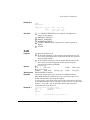
MACHXL Software User's Guide
© 1993 Advanced Micro Devices, Inc.
P.O. Box 3453 TWX: 910339-9280
Sunnyvale, CA 94088 TELEX: 34-6306
TOLL FREE: 800-538-8450
APPLICATIONS HOTLINE:
800-222-9323 (US)
44-(0)-256-811101 (UK)
0590-8621 (France)
0130-813875 (Germany)
1678-77224 (Italy)
TEL: 408-732-2400
Advanced Micro Devices reserves the right to make changes in
specifications at any time and without notice. The information furnished
by Advanced Micro Devices is believed to be accurate and reliable.
However, no responsibility is assumed by Advanced Micro Devices for its
use, nor for any infringements of patents or other rights of third parties
resulting from its use. No license is granted under any patents or patent
rights of Advanced Micro Devices.
Epson® is a registered trademark of Epson America, Inc.
Hewlett-Packard®, HP®, and LaserJet® are registered trademarks of
Hewlett-Packard Company.
IBM® is a registered trademark and IBM PC is a trademark of
International Business Machines Corporation.
Microsoft® and MS-DOS® are registered trademarks of Microsoft
Corporation.
PAL® and PALASM® are registered trademarks and MACH and MACHXL
are trademarks of Advanced Micro Devices, Inc.
Pentium is a trademark of Intel Corporation.
Wordstar® is a registered trademark of MicroPro International
Corporation.
Document revision 1.2
Published October, 1994. Printed inU.S.A.
ii
Contents
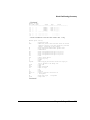
Chapter 1. Installation
Hardware Requirements
2
Software Requirements
3
Installation Procedure 4
Updating System Files 6
AUTOEXEC.BAT
7
CONFIG.SYS 7
Creating a Windows Icon for MACHXL
Chapter 2. Processing a Design
Design Flow 12
Program Module Descriptions 13
Structure of a MACHXL Design File 15
Creating a New Design
16
Using the New Design Form 16
Creating a New Design with the Text Editor
Opening an Existing Design 20
Using the Text Editor 21
Compiling the Design 24
Viewing Compilation Results 25
Back-Annotating the Design File
25
Simulating the Design 26
Downloading the JEDEC File 28
Standard PLD Programmer
28
JTAG Programming Cable
28
Disassembling a Compiled Design
28
Processing a Simple Design
30
Creating the Declaration Segment
31
Writing the Equations 39
Writing the Simulation Statements
40
Compiling the Design 41
Getting a Problem Design to Fit
43
8
20
Chapter 3. Design Examples
Multiplexer
50
Comparator
51
Left/Right Shifter
52
Barrel Shifter 53
Simple 3-Bit Counter 54
iii
Decoder
56
Up-Down Counter and Up-Counter with Parallel Load
Data Acquisition System
58
Moore State Machine 60
57
Chapter 4. Menu Reference
Overview
65
Screen Layout 65
Choosing Menu Commands
66
Preserving Menu Settings
69
File Menu
70
Begin New Design
70
Retrieve Existing Design
71
Change Directory
72
Set Up
73
Working Environment 73
Compilation Options 75
Compilation Options Form
76
MACH Fitting Options Form 77
Simulation Options
87
Logic Synthesis Options
89
Go To System 95
Quit
96
Edit Menu
97
Text File 97
Auxiliary Simulation File
97
Other File 98
Run Menu
98
Compilation
99
Compilation Options 100
Logic Synthesis Options
100
MACH Fitting Options 101
Run-Time Status Display
101
Output Files 102
Simulation 102
Both
103
Other Operations
103
Modify Pin & Node Numbers 104
iv
Disassemble From
105
Intermediate File 105
Jedec
105
Recalculate JEDEC Checksum 107
View Menu
108
Execution Log File
108
Design File 109
Fitter Reports 109
Fitting
109
Place/Route Data
109
Timing Analysis
109
JEDEC Data 110
Simulation Data
110
All Signals
111
Trace Signals Only
111
Printing the Simulation History
112
Waveform Display
113
All Signals
113
Trace Signals Only
114
Printing a Waveform 114
Current Disassembled File
115
Other File 115
Download Menu
116
Download to Programmer
116
Program via Cable
117
View Configuration File
117
Create/Edit Configuration File 118
Chain File Editor Modes
120
Completing the JTAG File Editor Form
Program device
126
Review JTAG results 127
Review JTAG status 127
View/edit output file(s) 127
123
Chapter 5. Language Reference
Symbols and Operators
129
Keywords
131
Chapter 6. Equations Segment In Depth
Pairing 193
Implicit Pairing Rules and Behavior 193
v
Output Pairing 195
Input Pairing 196
MACH 1xx Designs
196
MACH 2xx (Except MACH215) Designs
198
MACH 4xx and MACH215 Designs
199
Explicit Pairing Rules and Behavior 199
Copying Logic with Braces { } 200
Output Pairing 200
Input Pairing 203
Polarity
205
The Two Components of Polarity
205
Controlling Polarity from the Equation
205
Controlling Polarity from the Pin Statement 206
Controlling Polarity from CASE Statements 206
Functional Equations 209
Controlling Three-State Output Buffers
209
Controlling Clocks
210
Specifying a Rising-Edge Clock
211
Specifying a Falling-Edge Clock
211
Specifying a Product-Term Clock
212
Global Clock Acquisition
212
Controlling Set and Reset
214
Sharing Set and Reset 215
Vectors 216
Ranges of Pins or Nodes
216
Comma-Delimited Vectors
218
Radix Operators
219
IF-THEN-ELSE Statements 221
CASE Statements
222
Building State Machines with CASE Statements
Multiple State Machines
230
The "Don't-Care" Logic-Synthesis Option
237
MINIMIZE_ON and MINIMIZE_OFF 241
224
Chapter 7. Simulation Segment In Depth
Overview
245
Creating a Simulation File
246
Simulation Command Summary
246
Simulation Segment vs. Auxiliary File 248
Considerations 249
Vectors In Simulation 250
vi
SETF and PRELOAD 250
CHECK and CHECKQ 251
CLOCKF
252
TRACE_ON
252
Flip-Flops
252
Buried Nodes 253
Latches
253
Output Enable 253
Preloaded Registers
254
Verified Signal Values 254
Viewing Simulation Results
254
All Signals 255
Trace Signals Only
257
Text Display, Non-Vectored
258
Text Display, Vectored 259
Waveform Display, Non-Vectored
260
Waveform Display, Vectored 261
Using Simulation Constructs 261
For Loop 261
While Loop 262
If-Then-Else 262
Design Examples
263
Boolean Equation Design
263
State Machine Design 266
Notes On Using the Simulator 267
Modeling of Registers and Latches
268
Programmer Emulation at Power-Up 268
Power-Up Sequence
269
Software Preload Sequence
269
Full Evaluation of Input Pins 270
Clock Polarity 270
Driving Active-Low Clocks
271
Product Term-Driven Clocks 273
Simultaneous Events 274
Power-Up Preload On Floating Pins 274
Output Buffers 274
Input Signal Ordering 275
Preventing Unexpected Simulation Behavior 276
Placement Information Missing
276
Set/Reset Signals Swapped
276
Set/Reset Signals Treated As "Don't Care"
277
Uncontrollable Power-Up Conditions 277
vii
Chapter 8. Using the Fitter
Overview
281
The Fitting Process
281
Initialization 281
Normalization 282
Design Rule Check
282
Block Partitioning
282
Iterative versus Non-Iterative Partitioning
283
Manual Partitioning 284
Resource Assignment (Placement and Routing)
Designing to Fit
285
Methodology 285
Analyze Device Resources
286
Clock Signals
286
All Devices
286
MACH 3xx/4xx
286
MACH 215/3xx/4xx
287
Set/Reset Signals 288
Available Set and Reset Lines 288
MACH 3xx/4xx
288
Interaction of Set and Reset Signals
(All Devices Except MACH215)
288
Reserving Unused Macrocells and I/O Pins
289
Product Terms
290
Strategies for Fitting Your Designs
291
Fitting with Unconstrained Pinout
293
Fitting with Constrained Pinout
293
Interconnection Resources
295
Oversubscribed Macrocells and/or Inputs
295
Large Functions at the End of a Block 296
Adjacent Macrocell Use
297
Grouping Logic
297
Setting Compilation and Fitting Options
298
Reducing Non-Forced Global Clocks 298
Gate Splitting
298
All MACH Devices
300
MACH 3xx/4xx Devices
300
Failure to Fit on Second Pass 302
Understanding Global Clock Signals 303
284
viii
Balancing Clock Resources and Requirements 303
Global Clock Rules
304
Conditions Forcing Placement at a Global Clock Pin
Manually Forcing a Clock Signal to be Global 306
Conditions Forcing Non-Global Clocks 307
Resolving Contradictions
308
Chapter 9. Report Files
Overview
311
Log File
312
Fitting Report 318
Header Information
318
MACH Fitter Options 318
Device Resource Summary
320
Block Partitioning Summary 322
Signal Summary
324
PRESET, RESET and OUTPUT ENABLED
Signal Summary
327
Tabular Information 328
Fitting Status 338
Place and Route Data Report 339
Unplaceable Designs 340
Unroutable Designs
340
Place and route processing time
341
Place/Route Resource and Usage tables
341
Signal Fan-Out Table 343
Device pin-out list
344
Block information
345
Macrocell (MCell) Cluster Assignments
345
Maximum PT Capacity
350
Node-Pin Assignments 351
IO-to-Node Pin Mapping
353
IO/Node and IO/Input Macrocell Pairing Table
Input and Central switch matrix tables
357
Input Multiplexer (IMX) Assignments 357
Logic Array Fan-in 359
Using Place and Route Data to Limit Placements
Timing Analysis Report
364
TSU
366
TCO
367
TPD
368
305
356
362
ix
TCR
369
Failure Reports
Failure to Partition
Failure to Place
Failure to Route
370
370
372
373
Chapter 10. Device Reference
MACH Family Features Summary
377
MACH Features Locator, Part 1
378
MACH Features Locator, Part 2
379
MACH 1xx/2xx Design Considerations 380
Product Term Cluster Steering
380
Default Clock 380
XOR with D-Type Flip-Flops 381
T-Type Flip-Flops
381
Latches
382
MACH 1xx Latch Emulation 382
MACH 2xx Hardware Latches 383
Registered Inputs
384
Node Feedback vs. Pin Feedback
387
Registered Output with Node Feedback
or Pin Feedback
388
Combinatorial Output with Node Feedback
or Pin Feedback
391
Global Set and Reset 392
PAL22V10-Compatible Set/Reset Behavior
393
MACH 1xx/2xx Power-Up
393
Synchronous vs. Asynchronous Operation
393
Powerdown Feature
393
MACH 3xx/4xx Design Considerations 394
Cluster Size
394
Default Clock 395
XOR with D-Type Flip-Flops 395
T-Type Flip-Flops
396
Latches
399
MACH 3xx/4xx Hardware Latches
399
MACH 2xx/3xx/4xx vs. MACH 1xx
Latch Implementation 400
Registered Inputs (MACH 4xx Devices Only) 401
Zero Hold Time for Input Registers
402
Node vs. Pin Feedback 403
x
Registered Output with Node Feedback
or Pin Feedback
404
Combinatorial Output with Node Feedback
or Pin Feedback
407
Flexible Clock Generator
408
Global Set and Reset 409
Set/Reset Compatibility
410
PAL22V10 Register Behavior 411
Controlling MACH 3xx/4xx Set/Reset Behavior
412
Set/Reset in MACH 3xx/4xx Asynchronous Macrocells 413
Higher Block Utilization with the Set/Reset
Selector Fuse 414
MACH 3xx/4xx Power-Up
415
MACH 3xx/4xx Asynchronous Macrocell
Power-Up Operation 416
Set/Reset Design Recommendations 416
Synchronous vs. Asynchronous Operation
417
Synchronous Mode
418
Asynchronous Mode
419
Forcing Configuration as a Synchronous Macrocell
419
Cross-Programming MACH435 Designs
to the MACH445 Device
421
MACH110 Pin and Node Summary
423
MACH111 Pin and Node Summary
425
MACH120 Pin and Node Summary
427
MACH130 Pin and Node Summary
430
MACH131 Pin and Node Summary
433
MACH210 Pin and Node Summary
436
MACH211 Pin and Node Summary
438
MACH215 Pin and Node Summary
440
MACH220 Pin and Node Summary
442
MACH231 Pin and Node Summary
445
MACH355 Pin and Node Summary
448
MACH435 Pin and Node Summary
453
MACH445 Pin and Node Summary
456
MACH465 Pin and Node Summary
460
Appendix A. State Segment In Depth
Overview
468
Defining Moore and Mealy Machines 469
Creating State-Machine Equations
470
xi
Condition Equations 471
Transition Equations 471
Output Equations
472
State-Machine Example
472
Default Branches
474
Global Defaults
474
Local Defaults 474
Assigning State Bits 475
Automatic State-Bit Assignment
475
Manual State-Bit Assignment 476
Choosing State-Bit Assignments
477
Example Using Manual State-Bit Assignment 479
Using State Bits as Outputs 480
Initializing a State Machine 481
MACH 1xx/2xx Devices
481
MACH 3xx/4xx Devices
481
Illegal State Recovery 482
Clocking a State Machine
484
Example Using State Bits As Outputs, Start-Up,
and CLKF
485
Multiple State Machines
486
Appendix B. Glossary
Appendix C. Creating a LIM File
Overview
359
LIM File Conventions 360
Syntax 360
BLOCK Statement
360
Parameters
362
Appendix D. How to Report a MACHXL Software Problem
12
1
Installing the MACHXL Software
Contents
Hardware Requirements
2
Software Requirements
3
Installation Procedure 4
Updating System Files 6
AUTOEXEC.BAT
7
CONFIG.SYS 7
Creating a Windows Icon for MACHXL
8
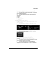
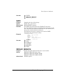
The MACHXL ® software installation process takes about 10 minutes.
Note: Installing MACHXL software does not affect PALASM ®
software that is installed on the same computer, as long as each
application is installed in its own directory. Unless you specify
otherwise, PALASM software is installed in a directory named
\PALASM and MACHXL software is installed in its own directory,
named \MACHXL.
Chapter 1: Installing the MACHXL Software
1
Hardware Requirements
MACHXL software is supported in single-user, non-networked
environments . The following hardware is required:
A.
An IBM ® PC or 100% compatible computer equipped with a 386,
486, or Pentium microprocessor.
B.
A minimum of 500 kilobytes (kB) of system RAM available after
all device drivers and TSRs have been installed. At least eight megabytes
(MB) memory is recommended. More memory may be required for
extremely large designs.
C.
A minimum of 6 MB of hard disk space available for MACHXL
software (separate from disk space used for PALASM software, if installed).
An additional 5 MB of free disk space is recommended for processing
designs.
D.
A 3-½" floppy disk drive.
E.
An EGA, VGA, or Super VGA monitor and graphics adapter.
Note: If you are using a monochrome screen with a graphics board,
use the following commands to set up your system after installing
the software:
CD \MACHXL\DAT [Enter]
DEL MACHXL.PCX [Enter]
SET MODE=MONO [Enter]
(Include the last command in your AUTOEXEC.BAT file also.)
Deleting the graphics file MACHXL.PCX forces the software to
display a text-based start-up screen that is easier to read on
monochrome screens, but has no other effect on software operation.
F.
Optionally, a parallel port for programming MACH devices that
have JTAG via cable. 5-Volt in-circuit JTAG programming kits for MACH
devices with JTAG are available from AMD.
G.
Note: The JTAG cable cannot be used with some software keys.
Remove any software keys from the parallel port before attaching
the JTAG cable to the parallel port of your PC. Attach the other end
to the 10 pin header on your JTAG board, as shown in the
MACHPRO programming manual found in the 5-Volt In-Circuit
JTAG Programming kit.
Optionally, one of the following printers :
Chapter 1: Installing the MACHXL Software
2
Software Requirements
IBM ProPrinter
Epson® FX 80 series
HP® LaserJet® and HP LaserJet Series II
(The HP LaserJet printers must include a font cartridge with
line-drawing capability, such as cartridge #HP3659A.)
Note: All printer output from the MACHXL software is text-based
except for the simulation waveforms, which use the line-drawing
characters of the extended IBM character set.
Note: Refer to the README file on disk 1 for information that
became available after this user's guide was printed.
Software Requirements
The minimum software requirement, which must be met before installing
and running the MACHXL software is listed below.
A.
MS-DOS ™ version 5.0 or later
B.
Proper software driver files for periphe ral devices
MACHXL software can be installed and run in a DOS box under Microsoft
Windows version 3.1 or higher. Directions on creating a Windows icon for
MACHXL are presented later in this chapter.
Note: Check the README file on disk 1 for the latest information
on OS/2and Windows NT support.
Note: You cannot run the MACHXL software from a floppy disk.
You must use the MACHXL installation program to install the
MACHXL software; simply copying the files to your hard disk does
not work. The steps below guide you through the installation and
configuration process.
Installation Procedure
Before you begin, you may want to check the path (typically C:\) to the file
COMMAND.COM so you can complete the installation form appropriately.
1.
Place installation disk 1 into drive A or drive B.
2.
From the DOS prompt, type
A:INSTALL and press the Enter key
or to install from drive B, type
B:INSTALL and press the Enter key
Wait for the MACHXL title screen to appear.
Chapter 1: Installing the MACHXL Software
3
Installation Procedure
3.
Press any key to proceed with the installation.
The installation menu and form appears; the menu covers part of
the form. The menu has two options:
Install MACHXL Software installs the software and related files.
You must use this command initially.
Reinitialize MACHXL Setup files reinstates the standard
SETUP.MXL file, and updates the CONFIG.SYS and AUTOEXEC.BAT files
to let them run MACHXL software.
4.
Select Install MACHXL Software and press the Enter key.
The menu is dismissed and the form is now completely visible, as
shown on the next page.
Note: If you do not ask the installation program to update files
automatically, the changes added to the dummy files CONFIG.M94
and AUTOEXEC.M94, or to files you specify In this case, you may
need to update information in the AUTOEXEC.BAT or
CONFIG.SYS files manually before you can use the MACHXL
software. See the "Updating System Files" section later in this
chapter for details. If no changes are required to AUTOEXEC.BAT
or CONFIG.SYS, no changes are made.
Note: As of this printing, AMD could not guarantee support in
OS/2 and network environments. See the README file on disk 1
for any last minute information on support for Windows NT, OS/2,
and network environments.
5.
To change options in the form, use the up- and down-arrow keys
to highlight the desired field, type the appropriate information, then press
the Enter key. After you press the Enter key, the next field on the form is
automatically highlighted.
6.
The default for the field Which parallel port will be used for programming
via cable? is lpt1. This is the port used for programming MACH devices with
JTAG. To change it, use the up- and down-arrow keys to highlight the
desired port (lpt1, lpt2 or lpt3), then press the Enter key.
Chapter 1: Installing the MACHXL Software
4
Updating System Files
Note: You must select a parallel port for programming via cable,
even if you do not plan to use this feature. The port selection may be
changed after installation through the Download menu, under
Download:Program via cable:Program Device,
Device as shown in Chapter 4,
"Menu Reference."
7.
When you are finished making changes to the data-entry fields
on the form, press the F10 key to confirm your settings.
A window opens in the lower half of the screen and the process
begins. Messages keep you informed and prompt you to insert disks as
required. A message signals the successful completion of installation.
8.
If you did not ask the installation program to change the
AUTOEXEC.BAT and CONFIG.SYS files for you, follow the instructions in
the "Updating System Files" section, below. Otherwise, proceed directly to
step 9.
9.
Remove the last installation diskette from the floppy drive and
restart the computer by holding down the Ctrl and Alt keys while you press
the Del key.
Updating System Files
You are asked about updating the AUTOEXEC.BAT and CONFIG.SYS files
on the installation form. The following discussions indicate the information
that is added during the automatic update. If you did not specify an
automatic update, you must ensure that this information appears in the
appropriate file.
Chapter 1: Installing the MACHXL Software
5
Creating a Windows Icon for MACHXL
AUTOEXEC.BAT
Note: If you entered the letter N in the update AUTOEXEC.BAT field,
you must manually edit the file to include the commands listed
below. Remember to edit AUTOEXEC.BAT and restart your
computer before invoking MACHXL.
The following information must appear in the AUTOEXEC.BAT file
before you can use the MACHXL software.
The PATH statement must include the directory containing the
MACHXL executable files (named \MACHXL\EXE by default).
For example, if your old path statement was
PATH C:\DOS;C:\UTIL;C:\CAD
...and your system boots on drive c:, your new path statement
should look like this:
PATH C:\MACHXL\EXE;C:\;C:\DOS;C:\UTIL;C:\CAD
A new variable that indicates the starting directory for the
software:
SET MACHXL=C:\MACHXL\
Note: If you are using a monochrome screen, add the following line
to your AUTOEXEC.BAT file:
SET MODE=MONO
CONFIG.SYS
Note: If you entered the letter N in the update CONFIG.SYS field, you
must manually edit the file so that the FILES= variable is set to 35
or greater.
If your CONFIG.SYS file already contains a FILES= environment
variable and if the FILES= variable is 35 or greater, no change is
required. Depending upon your system, it may be necessary to have
FILES= to more than 35 if you have network drivers and TSRs. If
the FILES= variable does not exist or is less than 35, add the
following line to the CONFIG.SYS file:
FILES=35
Creating a Windows Icon for MACHXL
Chapter 1: Installing the MACHXL Software
6
Creating a Windows Icon for MACHXL
Although MACHXL is not a Windows application, MACHXL may be run in a
DOS box under Windows or Windows NT. To create a Windows icon for
MACHXL software after you have installed it, follow these steps:
1.
Start the Windows File Manager.
2.
Drag the file MACHXL.PIF from the \MACHXL\DAT directory
to the Program Manager window of your choice. A place holder icon appears
in the window. (If you are using Windows NT, drag the MACHXLNT.PIF
file instead of the MACHXL.PIF file.)
3.
Select this new place holder icon by clicking the mouse button
once.
4.
Modify the properties of the MACHXL place holder icon by
pressing ALT+ENTER. Enter the path to the file MACHXL.PIF or
MACHXLNT.PIF. For example, if MACHXL is installed on the C drive in the
directory MACHXL, type "C:\MACHXL\DAT\MACHXL.PIF" or
"C:\MACHXL\DAT\MACHXLNT.PIF".
5.
Choose the Change Icon button, then enter the drive and location
of MACHXL and its icon in the \MACHXL\DAT directory. For example, if
MACHXL is installed in C:\MACHXL, type
"C:\MACHXL\DAT\−AMD.ICO".
The MACHXL software icon (a green AMD logo) is displayed.
6.
Choose the OK button.
Note: If you have installed MACHXL anywhere other than in
c:\MACHXL, you must also update the MACHXL.PIF file. Use the
PIF editor to change the path under "Program Filename" to
correctly represent your own path to the
MACHXL\EXE\MACHXL.EXE file. Save the corrected
MACHXL.PIF file.
Note: When you start MACHXL software for the first time using the
Windows icon, you will end up in the C:\ or in the C:\windows
directory. Once you change to a design directory, MACHXL will
remember that directory. The next time you start MACHXL
software, you will automatically be placed in your design directory.
Note: For more information on creating Windows icons, refer to
your Microsoft Windows documentation.
Chapter 1: Installing the MACHXL Software
7
2
Processing a Design
Contents
Design Flow 12
Program Module Descriptions 13
Structure of a MACHXL Design File 15
Creating a New Design
16
Using the New Design Form 16
Creating a New Design with the Text Editor
Opening an Existing Design 20
Using the Text Editor 21
Compiling the Design 24
Viewing Compilation Results 25
Back-Annotating the Design File
25
Simulating the Design 26
Downloading the JEDEC File 28
Standard PLD Programmer
28
JTAG Programming Cable
28
Disassembling a Compiled Design
28
Processing a Simple Design
30
Creating the Declaration Segment
31
Writing the Equations 39
Writing the Simulation Statements
40
Compiling the Design 41
Getting a Problem Design to Fit
43
20
Chapter 1: Installing the MACHXL Software
9
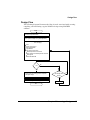
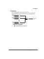
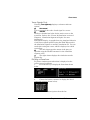
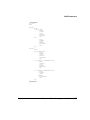
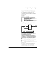
Design Flow
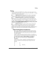
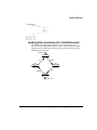
Design Flow
The following diagram illustrates the flow-of-work associated with creating,
compiling, and simulating a typical MACH ® design using MACHXL
software.
Begin
Use New Design form to enter header
information and pin declarations
Use text editor to specify the design using MACHXL
syntax. (Refer to Chapter 5 for syntax explanation)
Compile the design (see table of module functions
on the next page)
Parser
Boolean Post-Processor
State SyntaxExpander
Logic Minimizer
Fitter (major functions follow)
Partition equations into PAL blocks
Place equations at individual pins and macrocells
Route signals
Assemble JEDEC file
Fit ?
No
Yes
Back-annotate design to write placement data to pins
and nodes that were floating (positions unspecified
in the original design).
Simulate the design
Already
tried all likely Fitter
options?
No
Yes
Download the design to the device programmer
Revise design
End
Chapter 2: Processing a Design
12
Design Flow
Program Module Descriptions
Parser
Boolean PostProcessor
State Syntax
Expander
The parser checks the syntax of the input
design file (Design.PDS), creates an
intermediate file (Design.TRE) containing
the design information, and creates a log
file (Design.LOG) containing status
information and any warning or error
messages generated during the parsing
process. The log file is generated in the
directory that contains the design file to
which it refers. See Chapter 9, "Report
Files," for a detailed description of the log
file.
The Boolean Post-Processor runs after the
parser and, if the State Syntax Expander is
needed, again after that module. The
Boolean Post-Processor uses the TRE file
output from the preceding module to
substitute logical names for vectors and
groups, to convert IF-THEN-ELSE and
CASE statements into Boolean equations,
and to merge multiple equations written for
the same signal. Program outputs are
appended to the log file.
The State Syntax Expander processes the
TRE file output from the Boolean PostProcessor. The State Syntax Expander
converts state machine syntax (described in
Appendix A) into Boolean equations. State
machine designs implemented using CASE
and IF-THEN-ELSE statements do not
require processing by the State Syntax
Expander. Program status information is
appended to the Design.LOG file.
Chapter 2: Processing a Design
13
Design Flow
Logic Minimizer
Fitter
The Logic Minimizer uses the TRE file
output from the Boolean Post-Processor to
perform automatic logic reduction. The
Logic Minimizer eliminates redundancy,
reduces sum-of-products logic to its most
compact form, changes output polarity if
necessary to use the fewest product terms
possible, and does gate splitting. Program
status information is appended to the
Design.LOG file.
The Fitter is a suite of programs in itself: a
resource checker, partitioner, placer,
router, and report writer. The Fitter
creates the JEDEC file used to program the
MACH device. Program status information
is placed in three Fitter reports:
Design.RPT (general information),
Design.PRD (place-and-route information),
and Design.TAL (timing information). The
Fitter reports are generated in the
directory that contains the design file to
which they refer. See Chapter 9, "Report
Files," for detailed descriptions of the Fitter
reports.
Chapter 2: Processing a Design
14
Creating a New Design
Structure of a MACHXL Design File
All MACHXL design files have the same general structure, shown
below.
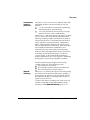
COMMENTS:
Required
DECLARATION SEGMENT
TITLE, PATTERN, REVISION, AUTHOR,
Keyword needed to begin segment:
COMPANY, and DATE statements
(none)
A CHIP statement to define the device
Pin declarations
Optional GROUP and STRING statements
Optional, but each design must
EQUATIONS SEGMENT
Boolean equations to control sum-of-products
logic
CASE and IF-THEN-ELSE statements
contain an EQUATIONS segment
or a STATE segment (and can
contain both)
Functional equations to control clocks, reset,
Keyword needed to begin segment:
preset, and output enable
EQUATIONS
State machines implemented with CASE
statements (see Chapter 6 for details)
STATE SEGMENT
Optional
Included for backward compatibility with
PALASM 4 designs. See Appendix A for details.
SIMULATION SEGMENT
Keyword needed to begin segment:
STATE
Optional
Simulation statements
(You can include simulation statements
directly in the design file, or create a separate
Keyword needed to begin segment:
SIMULATION
SIM file containing the simulation segment.
See Chapter 7 for details.)
Chapter 5, "Language Reference," lists and describes all of the
symbols, operators, and keywords used to create MACHXL designs,
including state and simulation syntax.
Creating a New Design
There are two ways to create a design file for use with MACHXL software:
Use the New Design form, which guides you through the creation
of the file's Declaration segment.
Chapter 2: Processing a Design
15
Creating a New Design
Create the entire design file with a text editor, then from the
MACHXL menu, select Retrieve existing design to continue processing.
Note: This chapter refers to a design called TEST2.PDS that
actually exists in the \MACHXL\EXAMPLES directory. Rather
than typing in a new design, you can load and compile the sample
file.
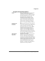
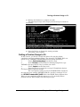
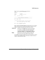
Using the New Design Form
To create a new design using the New Design form, follow these
steps:
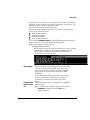
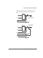
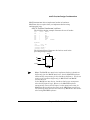
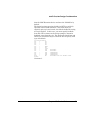
1. From the MACHXL menu, select Begin new design.
design
The following dialog box appears:
Input format:
New file name:
text
2. Type the name of the new design file in the New file name field.
Use any valid DOS file name and use the extension .PDS.
3. Press the F10 key to confirm your new file name and display the
New Design form.
The New Design form guides you through the creation of the
file's Declaration segment, which contains header information, the
device specification, and the pin declarations.
Chapter 2: Processing a Design
16
Creating a New Design
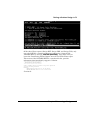
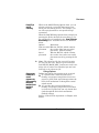
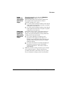
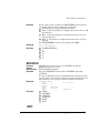
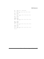
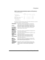
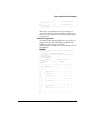
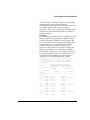
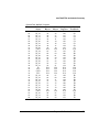
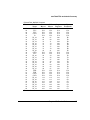
The form is described in the table that follows the figure.
Field Name:
Title
Function:
Enter the title of the design.
(Optional)
Enter the pattern number of
Pattern
the design.
(Optional)
Enter the revision number of
Revision
the design.
(Optional)
Enter your name.
Author
(Optional)
Enter your company name.
Company
(Optional)
Automatically enters today's
Date
date, but you can overtype
with another date.
Continued...
Refer to:
TITLE in Chapter 5
PATTERN in
Chapter 5
REVISION in
Chapter 5
AUTHOR in
Chapter 5
COMPANY in
Chapter 5
DATE in Chapter 5
Chapter 2: Processing a Design
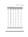
17
Creating a New Design
...Continued
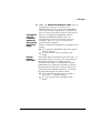
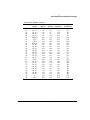
Field Name: Function:
Enter any name for the chip
ChipName
you will program with this
design.
Press the F2 key to select the
Device
MACH device on which the
new design will be
programmed. The displayed
list includes all supported
MACH devices.
Press the F2 key to select
P/N
PIN or NODE.
Select PIN to begin a PIN
statement. Select NODE to
begin a NODE statement.
Enter a question mark (?) to
Number
specify a floating pin or node.
Enter the pin or node
number to specify a preplaced pin or node (not
recommended).
Name
Enter a name for the pin or
node being declared.
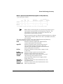
Continued...
Refer to:
CHIP in Chapter 5
CHIP in Chapter 5
PIN or NODE in
Chapter 5
PIN or NODE in
Chapter 5
? in the "Symbols
and Operators"
section of Chapter 5
"Strategies for
Fitting Your
Design" in
Chapter 8
PIN or NODE in
Chapter 5
Chapter 2: Processing a Design
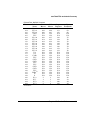
18
Creating a New Design
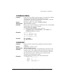
...Continued
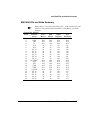
Field Name: Function:
Enter the name of the PIN
Paired with
with which you want to pair
PIN
the node being declared
(makes the node an output
register).
or
Enter the name of the NODE
with which you want to pair
the pin being declared
(makes the node an input
register).
Press the F2 key to select
Storage
COMBINATORIAL,
REGISTERED, LATCHED,
or BLANK (blank defaults to
combinatorial, but allows a
pin or node to take its
storage-type definition from
the node or pin with which it
is paired).
Press the F2 key to select
Comment
one of the available
comments, or leave this field
blank.
Refer to:
PAIR in Chapter 5
COMBINATORIAL,
REGISTERED,
LATCHED in
Chapter 5
N/A
Comments have no
effect on design
processing. Any
text that follows a
semicolon is treated
as a comment.
Note: To get help on filling out the form, press the F1 key.
To view a field's available options, press the Tab key as many times
as required to highlight the desired field and then press the F2 key
to display a list of options. Use the arrow keys to highlight the
desired option in the list and then press the Enter key to make your
selection.
4. When you are finished filling out the form, press the F10 key.
This saves the information you have entered and lets you
continue editing the design using the text editor. The text editor is
Chapter 2: Processing a Design
19
Opening an Existing Design
the one you specified when you set up the working environment.
(See the "Working Environment" section of Chapter 4, "Menu
Reference," for more information).
The MACHXL program loads the new design file into the text
editor automatically. Details on using the text editor are given in
the "Editing the Design File" section, later in this chapter.
Note: If you decide not to save your new design, press the Esc key.
The system prompts you to confirm that you want to exit without
saving. Type "Y" to confirm.
Creating a New Design with the Text Editor
You do not need to use the New Design form, but can do everything
from within the text editor. Details on using the text editor are
given in "Editing the Design File" later in this chapter.
Opening an Existing Design
To edit, compile, or otherwise interact with an existing design file from
within the MACHXL working environment, you must do the following:
1.
Specify the directory in which the design file is stored.
Do this by choosing Change directory from the File menu, typing
the directory's path, and pressing the Enter key.
For example, to change to the directory that contains the design
file referred to throughout this chapter, choose Change directory, type
\MACHXL\EXAMPLES, then press the Enter key.
2.
Specify the desired file.
Do this by choosing Retrieve existing file from the File menu. A
dialog box appears. You can either type the file name in the space provided,
or select the "*.pds" wild card specification. If you select the wild card
specification, a list of all files in the current directory that match the
specification appears. Use the arrow keys to highlight the desired file name,
then press the Enter key.
3.
Press the F10 key to confirm your choice and close the dialog box.
For example, to select the design file refer red to throughout this
chapter, choose Retrieve existing design, type TEST2.PDS, then press the F10
key.
Using the Text Editor
The MACHXL program calls a text editor under the following
circumstances:
When you save a new design you created using the New Design
form
Chapter 2: Processing a Design
20
Opening an Existing Design
When you choose Text File, Auxiliary Simulation File , or Other File from
the Edit menu
When you choose Program via cable from the Download menu to
edit a JTAG chain file
The text editor provided with the MACHXL software is invoked with
the path and file name \MACHXL\EXE\ED.EXE. If you prefer to
use a different editor from the one provided, you can specify that
editor's path and file name in the Working Environment form's Editor
Program field (File:Set
File:Set up:Working environment).
environment
Chapter 2: Processing a Design
21
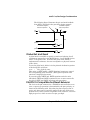
Opening an Existing Design
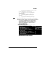
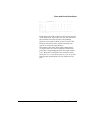
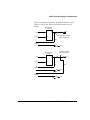
The Editor Program field in the Working Environment form, shown
below, is highlighted. The highlighted text will be replaced by any
characters entered from the keyboard.
The text editor provided with MACHXL emulates many of the
original WordStar ® key commands. You can also select functions
from a menu. Press the Esc key to display the menu. When the
menu is displayed, press the Esc key again to hide the menu.
Press F1 at any time to view a summary of available commands.
When you are finished editing your design, press the F10 key to save
your design and exit from the text editor program.
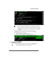
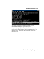
For example, to view and edit the design file you selected in the
previous section, choose Text file from the Edit menu. The editor loads
the design file as shown in the following figure.
Chapter 2: Processing a Design
22
Compiling the Design
Note: The design file TEST2.PDS uses "floating" pins and nodes
(pins and nodes that are not tied to specific pin and node numbers).
The symbol for a floating signal is a question mark ("?") in the PIN
or NODE statement where the pin or node number would normally
be entered.
To save your changes, exit from the editor, and return to the
MACHXL menu, press the F10 key. To return to the MACHXL
menu without saving your changes:
1. Press the Esc key to display the menu bar.
2. Type Q to open editor's the Quit menu, shown below.
3. Choose Quit all files.
files
Compiling the Design
The Compilation Options form allows you to choose the following operations:
Run all program m odules required to produce a JEDEC file
Run all required modules up to a certain point
Chapter 2: Processing a Design
23
Viewing Compilation Results
Even if you choose to run a complete compilation, you can terminate
compilation by pressing the Esc key. Compilation will terminate after the
current program module completes its task.
In this session, you will request a complete compilation (the default setting
of the Compilation Options form). If you have changed the setting of the
Provide compilation options on each run? form (File:Set
File:Set up:Working environment)
environment from
"Y" to "N," you will not perform steps 1 through 3.
1.
From the MACHXL menu, select Compilation from the Run menu.
The Compilation Options form appears.
2.
Press the F10 key to accept the default setting, "Run all
programs."
The Logic Synthesis Options form appears.
3.
Press the F10 key to accept the default settings.
The MACH Fitting Options form appears.
4.
Press the F10 key to accept the default settings and begin
compiling.
The progress of the compilation/fitting sequence appears in the large text
window. After each process module completes its portion of the compilation
process, a status message appears on the screen. The status message tells
whether the program ran to a successful completion, and gives the number
of errors and warnings it generated.
When processing is complete, the log file appears in the view
window. Use the PgUp and PgDn keys or the arrow keys to scroll through
the log file. Press the Esc key to close the view window when you are done.
Viewing Compilation Results
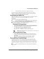
The View menu, shown below, is an easy way to view the
reports generated by the compilation programs.
The most commonly used reports are:
Execution Log File Contains status, warning, and error
messages, if any, from the compilation
and Fitter execution.
Chapter 2: Processing a Design
24
Back-Annotating the Design File
Fitter Reports
Three reports that contain general
Fitter data, place-and-route data, and
timing data. By default, these files are
saved as Design.RPT, Design.PRD and
Design.TAL, respectively. Refer to
Chapter 8, "Using the Fitter," and
Chapter 9, "Report Files," for details.
Back-Annotating the Design File
The design file used in the preceding examples did not include pin and node
placement information, because the pins and nodes were declared as
"floating" (using the "?" float operator). If you want to rerun the Fitter,
providing specific pin numbers not only speeds the process, but also provides
a useful verification that the pinout reported by the Fitter on one run can be
refitted on a subsequent run.
The MACHXL software offers a simple way to transfer the placement
information to the original design file:
1.
Choose Other operations... from the Run menu.
A pop-up menu of available operations appears.
2.
Choose Modify pin and node numbers... from the pop-up menu.
A pop-up menu of available operations appears.
3.
Choose Use last successful placement.
placement
The MACHXL software replaces the floating-pin and floating-node placeholder symbols (?) for each signal in the PIN and NODE declarations with
the actual locations used during the last successful fitting of the design.
This process is called back-annotation.
These changes are made directly to the original design file,
TEST2.PDS.
Chapter 2: Processing a Design
25
Simulating the Design
After the back-annotation process is complete, the results are
displayed in the view window. Press the Esc key to return to the MACHXL
menu.
Simulating the Design
1.
Choose Simulation from the Run menu.
The Simulation Options form appears. This form gives you the option of
using simulation statements contained in the current design file itself, or of
using a separate, auxiliary simulation file . Auxiliary simulation files (SIM
files) have the same name as the design files to which they pertain, but use
the general form Design.SIM. For example, the auxiliary simulation file for
the current design would have the name TEST2.SIM.
Leave the default setting, "N," for the Use auxiliary simulation file
field and move to the Use placement data from field, using the arrow keys.
2.
Press the F2 key to display available settings.
The simulation program must know where pin and node signals
are positioned in the device. Because the original design file specified
floating signals, you must either back-annotate the signal names, as
described in step 3 of the previous section, or have the simulator consult the
placement file directly, by choosing the appropriate option from the
Simulation Options form.
For 1xx/2xx designs
In the previous section you back-annotated the design file with the signal
placement information, so you can specify either the design file or the last
successful placement as the source of placement data.
For 3xx/4xx designs
In order to generate test vectors, the simulator needs more information than
is contained in the design file, so you must specify "last successful
placement."
3.
Select Last successful placement.
placement
4.
Press the F10 key to confirm your selection and begin simulating
the design.
When the simulator finishes the job, it displays a completion message.
Chapter 2: Processing a Design
26
Downloading the JEDEC File
5.
Press the Esc key to dismiss the completion message.
You can now view the simulation results from the View menu. Refer to
Chapter 7, "Simulation Segment In Depth," for details on the simulation
segment and the output of the simulator program.
Downloading the JEDEC File
When your design has been fit successfully and simulation shows the desired
behavior, you are ready to download the JEDEC file to the device
programmer.
There are two ways to progam MACH devices:
By downloading the finished JEDEC file to a device programmer
(for non-JTAG devices: MACH 1xx/2xx and MACH435 devices)
Directly from your PC using the MACH-compatible JTAG cable
(for MACH355, MACH445, and MACH465 devices)
Standard PLD Programmer
Use the download software provided with your device programmer to
download the JEDEC file. The file is stored in the same directory as
the design file, and has one of the following names:
Design.JED A standard JEDEC fuse data file
Design.JDC A JEDEC fuse data file with test vectors
Note: Refer to the programmer documentation for instructions on
using the programmer.
JTAG Programming Cable
Connect the JTAG cable to the MACH device as described in the
5V In-Circuit Programming Development Kit , available separately
from AMD.
Refer to the "Program via Cable" section of Chapter 4, "Menu
Reference," in this document for programming instructions.
Disassembling a Compiled Design
Occasionally you may need to view the results of the minimization and
expansion processes in a sum-of-products format. To do this, you need the
intermediate file and to get this, you must interrupt the compilation process.
You can stop compiling a design after any program module, in either of two
ways:
Select a termination point prior to fitting from the Compilation
Options form.
Chapter 2: Processing a Design
27
Processing a Simple Design
Press the Esc key while the design is being compiled to stop
processing after the current program module.
The Parser creates an intermediate TRE file and a LOG file (Design.LOG).
The Boolean Post-Processor, State Syntax Expander, and Minimize operate
on and modify the TRE file, and add to the log file. (The Logic Minimizer
creates a PLA file in addition to updating the TRE file; the Fitter uses the
PLA file rather than the TRE file for the remainder of the compilation
process.)
The MACHXL program includes utilities to disassemble the intermediate
TRE file. The disassembled file contains Boolean equations, and is especially
useful to check the logic of your design before and after minimization.
Disassemble the current design as follows:
1.
Choose Other operations... from the Run menu.
2.
Choose Disassemble from... from the pop-up menu.
Another pop-up menu appears.
3.
Choose Intermediate file from the pop-up menu.
You can also disassemble the JEDEC file , which is used to reconstruct a
design when the other files are missing.
Note: Many designers verify the functionality of the JEDEC file as
follows: 1) Run simulation on the design file and print out the
simulation results. 2) Disassemble the JEDEC file with pins and
nodes placed. 3) Recompile and simulate the disassembled and
print out the simulation results. 4) Compare the two sets of
simulation results to ensure identical behavior between design and
JEDEC.
MACHXL JEDEC files contain signal names. JEDEC files created
using other software may not contain this information. If you are
not using a MACHXL JEDEC file, you may need to back-annotate
signals between steps 2 and 3, above.
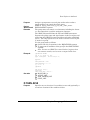
Processing a Simple Design
Chapter 2: Processing a Design
28
Processing a Simple Design
In this section, you will learn how to create and compile a simple design that
fits on a small MACH device (the MACH111) using all default settings for
compilation and fitting.
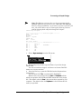
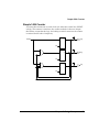
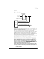
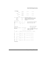
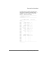
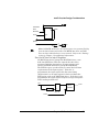
This design example defines the barrel shifter shown in the following block
diagram.
ENA
DATA[0..3]
4
4
Q[0..3]
CLK
ENA
SEL1
SEL2
Unlike a shift register, which shifts data bits one position to the left or right,
the barrel shifter shifts data a selectable number of positions to the left or
right.
In this example, the data inputs DATA[0], DATA[1], DATA[2], and DATA[3]
are represented by the vector notation DATA[0..3] and the outputs Q[0],
Q[1], Q[2], and Q[3] are represented by the vector notation Q[0..3]. 1 Each
data input's value (0 or 1) is mirrored in one of the outputs, but which of the
four outputs contains the value of a given data input is controlled by the
values of two selector inputs, SEL1 and SEL2.
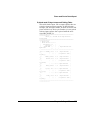
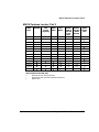
The values of the two selector inputs, SEL1 and SEL2, can define four
binary numbers: 00, 01, 10, and 11. The following table shows, for each of
the four possible selector input values, which data input is carried by each
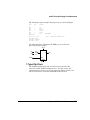
output.
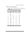
Q[3]
Q[2]
Q[1]
Q[0]
Mirrors
Mirrors
Mirrors
Mirrors
Input...
Input...
Input...
Input...
DATA[3]
DATA[2]
DATA[1]
DATA[0]
Selector 00
01
DATA[0]
DATA[3]
DATA[2]
DATA[1]
Input
10
DATA[1]
DATA[0]
DATA[3]
DATA[2]
Values
11
DATA[2]
DATA[1]
DATA[0]
DATA[3]
Creating the Declaration Segment
You can create the entire file using the text editor, or use the
MACHXL New Design form to create the declaration segment as
described in the "Creating a New Design" section earlier in this
chapter.
Chapter 2: Processing a Design
29
Processing a Simple Design
Note: The following exercises show you how to recreate the file
BARREL.PDS that was placed in your \MACHXL\EXAMPLES
directory during installation. If you take a moment to print this file
now, you will be able to refer to it during the following exercises
without skipping back and forth through this chapter.
;MACHXL Design Description
;------------------------------- Declaration Segment ----------TITLE
Barrel Shifter
PATTERN 1
REVISION 1
AUTHOR
J. Engineer
COMPANY AMD
DATE
8/28/94
CHIP Barrel MACH111
;------------------------------- PIN Declarations -------------PIN ?
DATA[0..3]
PIN ?
Q[0..3]
REGISTERED ;
PIN ?
SEL1
PIN ?
SEL2
PIN ?
RESET
PIN ?
CLK
PIN ?
ENA
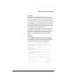
1. Choose Begin new design from the File menu.
2. In the dialog box provided, type the name of your first design,
FIRST.PDS.
You can use and mix of upper- and lower-case letters; DOS file
names are not case-sensitive.
3. Press the F10 key to open the PDS Declaration Segment form
shown below.
The first data field, Title,
Title is automatically highlighted.
Default values are provided fo r the Date and ChipName = fields,
which correspond to the DATE and CHIP statements in the design
file. The default value for Date is the current date reported by your
computer. The default value for ChipName = is derived from the file
name you specified.
Chapter 2: Processing a Design
30
Processing a Simple Design
4. Type the design title, "Barrel Shifter," and press the Enter key to
move the highlight field.
The Pattern field is now highlighted.
Note: You can also use the Tab, up-, and down-arrow keys to move
the highlight from one field to the next. Hold down the Shift key
while pressing the Tab key to move the highlight to the previous
field.
5. Type the value "1" for Pattern and press the Enter key.
6. Type the value "1" for Revision and press the Enter key.
7. Enter your own name for Author and press the Enter key.
8. Type your company name for Company and press the Enter key.
9. Press the Enter key twice to accept the default Date and
ChipName = entries.
A list of all supported MACH devices appears in the Device =
field's drop-down list.
10. Use the up- and down-arrow keys as required to highlight
MACH111 in the list, then press the Enter key.
The specified device, MACH111, appears in the Device = field as
shown on the next page.
Chapter 2: Processing a Design
31
Processing a Simple Design
11. Press the Enter key again to move to the first field in the P/N
(Pin/Node) list.
The P/N field is automatically filled with last pin/node type
specified. If the default type is the one you want, press the Enter
key to move to the Number field, otherwise press the F2 key to
display the list of available P/N types. (Use the empty pin/node type
to erase a pin or node statement.)
Chapter 2: Processing a Design
32
Processing a Simple Design
12. Press the F2 key to display the list of available pin/node types.
13. Use the up- and down-arrow keys to highlight "PIN," then press
the Enter key to place "PIN" in the P/N data field.
14. Press the Enter key again to move to the Number field.
You can specify an actual pin number or float the pin by typing a
question mark (?) instead of a pin number. 2 In most cases, the Fitter
is more likely to succeed in fitting the design if you float all pins and
nodes.
15. Type a question mark in the Number field and then press the
Enter key to move to the Name field.
You are about to define, with one statement, the four I/O pins
that will be used as data inputs to the barrel shifter. You do this by
specifying, as the pin name, a vector rather than an individual pin
name.3 A vector is a common name and a range of subscript values,
where the subscript differentiates individual pins or nodes from
others having the same common name.
Vectors are written as follows:
Common name Opening bracket Closing bracket
DATA[0..3]
Starting subscript number
Ending subscript number
Chapter 2: Processing a Design
33
Processing a Simple Design
16. Define a vector of four pins by typing the following information
in the Name field and then pressing the Enter key:
DATA[0..3]
Case is ignored; all of the following entries are equivalent:
DATA[0..3], data[0..3], DaTa[0..3].
The four pins so defined can hereafter in the design file be
referenced as a group ( DATA[0..3] ) or a subgroup ( DATA[0..1] or
DATA[2..3] ) or as individual pins ( DATA[0], DATA[1], DATA[2],
and DATA[3] ).4
17. Press the Enter key to leave the Paired with pin field empty.
18. Press the Enter key to skip over the Storage type field.
Pins DATA[0..3] are used as combinatorial inputs. If you do not
specify any storage type, the storage type COMBINATORIAL is
implied.
The highlight moves to the Comment field. Pressing the F2 key
allows you to choose "Input," "Output," or a blank field to fill the
comment field. The default is a blank field. Comments do not affect
design functionality, and have been omitted in this discussion for the
sake of brevity.
19. Press the Enter key to skip over the Comment field.
The pin/node type PIN is automatically inserted in the next P/N
field because PIN was the last type specified.
20. Press the Enter key to accept the P/N type PIN.
21. Type a question mark in the Number field and then press the
Enter key.
Next, you will define the vector of four outputs, Q[0..3].
22. Type the following and then pre ss the Enter key:
Q[0..3]
23. Press the Enter key to leave the Paired with pin field empty.
In fact, the pins Q[0..3] will be paired with output macrocells to
provide registered outputs, but in this example you will allow the
MACHXL software to perform implicit pairing. For a detailed
discussion of implicit pairing as well as other types of pairing, refer
to the "Pairing" section of Chapter 6, "Equations Segment In Depth."
Chapter 2: Processing a Design
34
Processing a Simple Design
24. Press the F2 key to display available choices for the Storage type
field.
25. Use the up- and down-arrow keys to highlight "REGISTERED,"
then press the Enter key.
26. Press the Enter key to skip over the Comment field.
The pin/node type PIN is automatically inserted in the next P/N
field because PIN was the last type specified.
27. Press the Enter key to accept the P/N type PIN.
28. Type a question mark in the Number field and then press the
Enter key.
22. Type the following and then press the Enter key:
SEL1
23. Press the Enter key to leave the Paired with pin field empty.
24. Press the F2 key to display available choices for the Storage type
field.
25. Use the up- and down-arrow keys to highlight the blank field,
then press the Enter key.
Both the "Combinatorial" and blank field settings produce the
same result in this case, because the default storage type is
combinatorial.
27. Complete the pin declarations for the remaining pins, using the
printout of the BARREL.PDS file as your guide.
Chapter 2: Processing a Design
35
Processing a Simple Design
28. When you are finished, press the F10 key to close the PDS
Declaration Segment form, save the design file, and load the design
file into the text editor.
Writing the Equations
(This section assumes that the text editor was invoked by the
MACHXL software as described in step 28 of the "Creating the
Declaration Segment" section.)
Position the cursor in the text file after the keyword EQUATIONS,
then type the following equations:
Q[0..3].RSTF=RESET
Q[0..3].CLKF=CLK
Q[0..3].TRST=ENA
Q[0]:= /SEL1*/SEL2*DATA[0]
+/SEL1* SEL2*Q[1]
+ SEL1*/SEL2*Q[2]
+ SEL1* SEL2*Q[3]
Q[1]:= /SEL1*/SEL2*DATA[1]
+/SEL1* SEL2*Q[2]
+ SEL1*/SEL2*Q[3]
+ SEL1* SEL2*Q[0]
Q[2]:= /SEL1*/SEL2*DATA[2]
+/SEL1* SEL2*Q[3]
+ SEL1*/SEL2*Q[0]
+ SEL1* SEL2*Q[1]
Q[3]:= /SEL1*/SEL2*DATA[3]
+/SEL1* SEL2*Q[0]
+ SEL1*/SEL2*Q[1]
+ SEL1* SEL2*Q[2]
Writing the Simulation Statements
(This section assumes that the text editor was invoked by the
MACHXL software as described in step 28 of the "Creating the
Declaration Segment" section.)
1. Position the cursor in the text file after the keyword
SIMULATION, then type the following commands:
TRACE_ON
data[3..0] q[3..0] sel1 sel2
clk
SETF RESET
ena
SETF DATA[3..0]= #H8
SETF /RESET ena
;---LOADING DATA
SETF /SEL1 /SEL2
CLOCKF CLK
CHECKQ Q[3..0]= #H8
;--Shifting one position to the right, three times
SETF /sel1 sel2
FOR X:= 1 TO 3 DO
Chapter 2: Processing a Design
36
Processing a Simple Design
BEGIN
CLOCKF CLK
END
CHECKQ Q[3..0]= #H1
;--Shifting two positions to the right, four times
SETF sel1 /sel2
FOR X:= 1 TO 4 DO
BEGIN
CLOCKF CLK
END
CHECKQ Q[3..0]= #H1
;--Shifting three positions to the right (same as one to the left),
;
four times
SETF sel1 sel2
FOR X:= 1 TO 4 DO
BEGIN
CLOCKF CLK
END
CHECKQ Q[3..0]= #H1
TRACE_OFF
2. Press the F10 key and then the Enter key to close the editor,
save all changes, and return to the MACHXL screen.
Compiling the Design
1.
2.
3.
4.
5.
Choose Compilation from the Run menu.
Press the F10 key to accept the default compilation options.
Press the F10 key to accept the default logic synthesis options.
Press the F10 key to accept the default MACH fitting options.
Wait for the Fitter to complete its tasks.
The following message will be displayed if the design is processed
successfully:
Chapter 2: Processing a Design
37
Processing a Simple Design
Indicates a successful fit
6. Press the Esc key to dismiss the message window.
Next, you will run the Simulator.
7. Choose Simulation from the Run menu.
The Simulation Options form appears as shown on the next page.
This form allows you to run simulation using simulation commands
stored in a file that is separate from the design file (not needed in
this case, because you included simulation commands in the design
file). This form also allows you to use pin/node placement data from
a source other than the last successful placement (not needed in this
case).
Chapter 2: Processing a Design
38
Processing a Simple Design
8. Press the down arrow to highlight the Use placement data from field.
9. Press the F2 key to display the available options.
10. Use the up- and down-arrow keys to select the "Last successful
placement" option.
11. Press the Enter key to confirm your choice.
12. Press the F10 key to accept the default settings and run the
simulator.
Chapter 2: Processing a Design
39
Getting a Problem Design to Fit
13. Wait for the Simulator to complete its tasks.
The following message will be displayed if the design is simula ted
successfully:
Indicates a successful
simulation
10. Press the Esc key to dismiss the message window.
Processing is now complete.
Getting a Problem Design to Fit
In this exercise, you will fit a design that fails to fit using the default
compilation and logic synthesis options. The design file, NOT2BIG.PDS, was
placed in your \MACHXL\EXAMPLES directory during installation.
1.
Choose Retrieve existing design from the File menu.
2.
In the File name field of the Retrieve Existing Design form, type
NOT2BIG, then press the F10 key to confirm your choice.
3.
Choose Compile from the Run menu.
4.
Press the F10 key as required to accept all Compilation Options
and Logic Synthesis Options settings.
The saved options settings in the file NOT2BIG.MXL, included in
the same directory with the NOT2BIG.PDS file, specifies a setting of "N" for
the SET/RESET treated as DONT_CARE? field of the MACH Fitting Options form.
When you run compilation with this option set to "N," the design fails to
partition and the Fitter displays the following message:
Chapter 2: Processing a Design
40
Getting a Problem Design to Fit
Of the three Fitter reports ( Design.RPT, Design.PRD, and Design.TAL), only
one—the .RPT file—contains partitioning information. Open the file
NOT2BIG.RPT by choosing View:Fitter reports:Fitting.
reports:Fitting Page down until you
locate the "Partitioning Failure Report" near the end of the Fitter report.
This section of the NOT2BIG.RPT file, reproduced below, provides
information that immediately suggests a solution.
*******************************
* PARTITIONING FAILURE REPORT *
*******************************
Signal 'SIGBE' cannot be placed in any block partition
for the following reasons:
BLOCK A RESET equation does not fit in the block.
BURIED REGISTER does not fit in the block.
Continued...
Chapter 2: Processing a Design
41
Getting a Problem Design to Fit
...Continued
BLOCK B RESET
BLOCK C RESET
BLOCK D RESET
BLOCK E RESET
BLOCK F RESET
BLOCK G RESET
BLOCK H RESET
equation does not fit in the block.
equation does not fit in the block.
equation does not fit in the block.
equation does not fit in the block.
equation does not fit in the block.
equation does not fit in the block.
equation does not fit in the block.
The following signals remain to be partitioned
( excluding pins used only as inputs )
RESESIGJNT
SIGBE
SIGBH
SIGBK
SIGBN
Notice that the equation that failed to fit in any block was a Reset equation.
The following fragment from the design file NOT2BIG.PDS shows a
multitude of .RSTF equations and no .SETF equations.
...
; Define event FF control inputs
sigbd.CLKF
=
clk1;
sigbe.CLKF
= sige;
sigbf.CLKF
= clk1;
sigbe.RSTF
= sigbd;
sigbf.RSTF
= sigbd;
sigbg.CLKF
=
clk1;
sigbh.CLKF
= / sige;
sigbi.CLKF
= clk1;
sigbh.RSTF
= sigbg;
sigbi.RSTF
= sigbg;
sigbj.CLKF
= clk1;
sigbk.CLKF
= / sigc;
sigbl.CLKF
= clk1;
sigbk.RSTF
= sigbj;
sigbl.RSTF
= sigbj;
sigbm.CLKF
=
clk1;
sigbn.CLKF
= sigc;
sigbo.CLKF
= clk1;
Continued...
Chapter 2: Processing a Design
42
Getting a Problem Design to Fit
...Continued
sigbn.RSTF
sigbo.RSTF
sigbp.CLKF
sigbq.CLKF
sigbr.CLKF
sigbq.RSTF
sigbr.RSTF
sigbs.CLKF
sigbt.CLKF
sigbu.CLKF
sigbt.RSTF
sigbu.RSTF
sigbv.CLKF
sigbw.CLKF
sigbx.CLKF
sigbw.RSTF
sigbx.RSTF
sigca.CLKF
sigcb.CLKF
sigcc.CLKF
sigcb.RSTF
sigcc.RSTF
sigcd.CLKF
sigce.CLKF
sigcf.CLKF
sigce.RSTF
sigcf.RSTF
sigba.CLKF
sigbb.CLKF
sigbc.CLKF
sigbb.RSTF
sigbc.RSTF
...
=
=
sigbm;
sigbm;
=
clk1;
= / sigf;
= clk1;
= sigbp;
= sigbp;
=
clk1;
= sigf;
= clk1;
= sigbs;
= sigbs;
=
clk1;
= / siga;
= clk1;
= sigbv;
= sigbv;
=
clk1;
= / sigd;
= clk1;
= sigca;
= sigca;
= clk1;
= / sigb;
= clk1;
= sigcd;
= sigcd;
=
clk1;
= / clk2;
=
clk1;
=
sigba;
=
sigba;
The SET/RESET treated as DONT_CARE? field of the MACH Fitting
Options form, when set to "Y," allows better utilization of limited block
Set/Reset resources in MACH 3xx/4xx devices.
5.
Press the Esc key to close the Fitter report. Then recompile the
design, this time setting the SET/RESET treated as DONT_CARE? field of the
MACH Fitting Options form set to "Y." The design now fits, as shown in the
following log entry:
Chapter 2: Processing a Design
43
Getting a Problem Design to Fit
When you fit a design by allowing the Fitter to treat any unspecified
condition (Set/Rest from the MACH Fitting Options form or
CASE/IF..THEN..ELSE from the Logic Synthesis Options form) as don't
care, you must be especially vigilant in your simulation and other qualityassurance analyses for undesired changes in design functionality. In the
exercise you just completed, no adverse effects result from the change to the
compilation options. The design fits and is usable on the original target
(MACH435) device.
Chapter 2: Processing a Design
44
3
Design Examples
Contents
Multiplexer
50
Comparator
51
Left/Right Shifter
52
Barrel Shifter 53
Simple 3-Bit Counter 54
Decoder
56
Up-Down Counter and Up-Counter with Parallel Load
Data Acquisition System
58
Moore State Machine 60
57
Chapter 2: Processing a Design
45
Multiplexer
The following design examples show how several commonly used design
elements are implemented using the MACHXL language. For your
convenience, the MACHXL design files for these design examples are
installed on your hard disk when you install the MACHXL software, in the
\MACHXL\EXAMPLES directory.
Multiplexer
This 8:1 multiplexer uses three select bits to route one of eight busses.
Unlike the multiplexer presented in the "Data Acquisition System" section of
this chapter, this multiplexer has been implemented with Boolean equations
rather than CASE statements.
To view the MACHXL implementation of this design, open the design file
MUX.PDS.
DATA[0..7]
00
DATB[0..7]
01
DATC[0..7]
10
DATH[0..7]
11
MUXOUT
SEL1
SEL2
SEL3
Features of Interest
Uses vectors
Implements a multiplexer using Boolean logic
Chapter 3: Design Examples
50
Comparator
Comparator
A fast comparator that compares two ten-bit busses.
The logic diagram for this design appears below. To view the MACHXL
implementation of this design, open the design file COMPARA.PDS.
INX[0]
IN[0]
INX[1]
IN[1]
COMPOUT
INX[9]
IN[9]
Features of Interest
Uses XOR statements in equations
Uses FOR..TO..DO in simulation
Chapter 3: Design Examples
51
Left/Right Shifter
Left/Right Shifter
Shift registers are widely used in communications and computer systems.
Shift registers can serialize data, which allows designers to minimize the
number of output pins and bus bits. This particular shift register performs
three operations:
Loads a new eight-bit byte of data (when the control line LOAD
is high and the device is clocked)
Shifts data left (when the control line LOAD is low, the control
line LR is high, and the device is clocked)
Shifts data right (when the control line LOAD is low, the control
line LR is low, and the device is clocked)
I[0..7]
AB[0..7]
CLK
LOAD
LR
RESET
To view the MACHXL implementation of this design, open the design file
LRSHIFT.PDS.
Features of Interest
Uses CASE statements
Uses vectors on both sides of a Boolean equation (that is,
transfers data from one bank of signals to another ng a single
statement)
Uses vectors of signals in both the Equations and Simulation
segments, including CHECK statements using vectors
Uses FOR..TO..DO statements for simulation
Chapter 3: Design Examples
52
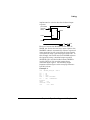
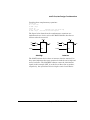
Barrel Shifter
Barrel Shifter
This design is discussed at length in Chapter 2.
DATA[0..3]
Q[0..3]
CLK
ENA
SEL1
SEL2
To view the MACHXL implementation of this design, open the design file
BARREL.PDS.
Features of Interest
All behavior specified using sum-of-products Boolean equations
Uses vectors of signals in both the Equations and Simulation
segments
Chapter 3: Design Examples
53
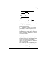
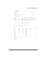
Simple 3-Bit Counter
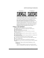
Simple 3-Bit Counter
A counter that increments on each clock cycle when the control line COUNT
is high. This counter is similar to the counter modules in the two designs
that follow, except that the logic for loading an initial count into the counter
is omitted for the sake of simplicity.
ENABLE
T
Q
B[0]
T
Q
B[1]
T
Q
B[2]
CLK
CLK
CLK
Chapter 3: Design Examples
54
Simple 3-Bit Counter
Note: T flip-flops are recommended for most counter designs since
these require fewer product-terms than do D flip-flops. Parallelloaded counters using D flip-flops require less logic for loading, but
these still need more product-terms than an equivalent T flip-flop
counter. For large counter designs the user should design one
lookahead carry bit for every 15 counter bits. The carry bit will be
the only input to the next PAL block from the present PAL block,
and input array resources will not be wasted.
Ripple counters may be a good choice for very large counter designs.
However, take into consideration the following caveats: Ripple
counters are slow and may require extra logic to avoid glitches.
Also, functional simulation of these counters will not show timing
delays and glitches.
Note: If you set the Optimize registers for D/T-type field of the Logic
Synthesis Options form ( File:Set up:Compilation options)
options to "Best for
device," the Fitter will automatically change D-type flip-flops to Ttype or vice versa to produce the most efficient implementation for
the target MACH device.
To view the MACHXL implementation of this design using D-type flip-flops,
open the design file 3COUNT_D.PDS. To view the MACHXL
implementation of this design using T-type flip-flops, open the design file
3COUNT_T.PDS.
Features of Interest
For the purpose of comparison, uses individual pin names in
places where other examples in this chapter typically use vector
notation
Chapter 3: Design Examples
55
Decoder
Decoder
Decoders, such as the one shown here, can be used for memory addressing,
where they select one of several memory devices. They can also be used to
demultiplex data and reroute clocks.
DATA[0]
DATA[1]
DATA[2]
DATA[3]
DATA[4]
DATA[5]
DATA[6]
DATA[7]
OUT0]
OUT[1]
OUT[2]
OUT[3]
OUT[4]
OUT[5]
SEL0
OUT[6]
SEL1
OUT[7]
SEL2
To view the MACHXL implementation of this design, open the design file
DECODE.PDS.
Features of Interest
In simulation, sets a vector of pins to a hexadecimal value
Chapter 3: Design Examples
56
Up-Down Counter and Up-Counter with Parallel Load
Up-Down Counter and Up-Counter with Parallel Load
This design is presented in four design files, each of which implements the
design in a different way:
The up-down counter with parallel load is implemented using
Boolean equations in the design file UDCNT.PDS.
The up-counter with parallel load is implemented using
IF..THEN..ELSE constructs in the design file CNTIF.PDS.
The up-counter with parallel load is implemented using CASE
constructs in the design file CNTCASE.PDS.
The up-counter with parallel load is implemented using Boolean
equations in the design file COUNTER.PDS.
In addition to incrementing the current count by one when counting is
enabled, the counter can be loaded with a new current count from a bank of
input pins or reset to zero at any time.
COUNT
LOAD
DATA[0..7]
COUNTER
(See up/down
counter
example
in this
chapter)
OE
TC[0..7]
8
8
8
Features of Interest
Shows several ways to implement equivalent logic
Chapter 3: Design Examples
57
Data Acquisition System
Data Acquisition System
This design (shown on the next page) contains the following subsystems:
A demultiplexer
A 4-to-1 multiplexer
A synchronous counter
A bidirectional multiplexer.
These subsystems are used in many data acquisition applications as well as
in computer applications. In this design:
Inputs are in the form of multiplexed data, which are
demultiplexed inside.
The demultiplexer consists of two sets of registers controlled by
different clock-enable logic. Therefore, each bank of registers will register a
different set of data. Such demultiplexing techniques are useful to save
device pins.
The adder and the multiplexer provide several addressing
choices for this real-time CPU-controlled system.
The counter loads data from external RAM, increments it, and
writes it back to the RAM.
The Bidirectional multiplexer provides multiplexing and parallel
communication between external buses and memory devices.
The following block diagram shows the overall design in pictorial form.
The design file is DATA_AQ.PDS.
Features of Interest
A realistic example of a moderately complex design that
combines several subsystems on the same device
Chapter 3: Design Examples
58
Data Acquisition System
8
MUXED_DATA[0..7]
8
A_DATA[0..7]
DEMUX
ADDER
ADD[0..7]
4-TO-1 MUX
8
RAMADDRESS[0..7]
B_DATA[0..7]
8
BUSADDR[0..7]
BUSDATA[0..7]
8
8
8
BI-MUX
COUNTER
MACH Device
Chapter 3: Design Examples
59
RAMDATA[0..7]
Moore State Machine
Moore State Machine
State machines are used in many different applications. There are many
state machine models available, the two most common (and the two
supported by MACHXL software) being the Moore and Mealy models.
Moore machines have a single set of outputs for each state; that is, outputs
are determined solely by the machine's current state. Mealy machines can
have different outputs in the same state. Mealy machine outputs are
determined by evaluating inputs as well as by the machine's current state.
The design presented here is not meant to perform any particular function,
but rather to illustrate Moore state machine design principles. To increase
its usefulness as a learning tool, this design is implemented in three
different ways:
Using CASE statements as described in Chapter 6, "Equations
Segment In Depth" (MOORE_C.PDS)
Using the MACHXL state machine language as described in
Appendix A, "State Segment In Depth" (MOORE_S.PDS) 5
Using Boolean equations (MOORE_B.PDS)
You can implement only one state machine in the STATE segment of any
design file. If your design contains multiple state machines, a CASE
implementation is usually the best choice.
Chapter 3: Design Examples
60
Moore State Machine
RESET
JUMP
JUMP
GO
JUMP
S5
out1 * /out2 * out3
S0
/out1 * /out2 * /out3
BACK
GO
S1
/out1 * /out2 * out3
BACK
GO
BACK
GO
BACK
S4
out1 * /out2 * /out3
GO
BACK
S2
/out1 * out2 * /out3
BACK
S3
/out1 * out2 * out3
JUMP
GO
JUMP
JUMP
For other examples of Moore and Mealy machines, see Appendix A, "State
Segment In Depth."
Features of Interest
Identical behavior generated using three different models
Full initialization and illegal state recovery logic in each design
State syntax example (MOORE_S.PDS) shows how to check state
names in the Simulation segment
Chapter 3: Design Examples
61
Moore State Machine
Chapter 3: Design Examples
63
4
Menu Reference
Contents
Overview
65
Screen Layout 65
Choosing Menu Commands
Preserving Menu Settings
File Menu
70
Begin New Design
70
Retrieve Existing Design
Change Directory
72
Set Up
73
Working Environment 73
Compilation Options 75
Compilation Options Form
MACH Fitting Options Form
Simulation Options
87
Logic Synthesis Options
Go To System 95
Quit
96
Edit Menu
97
Text File 97
Auxiliary Simulation File
Other File 98
Run Menu
98
Compilation
99
Compilation Options 100
Logic Synthesis Options
MACH Fitting Options 101
Run-Time Status Display
Output Files 102
Simulation 102
Both
103
Other Operations
103
66
69
71
76
77
89
97
100
101
Chapter 4: Menu Reference
Reference
63
Overview
Modify Pin & Node Numbers 104
Disassemble From
105
Intermediate File 105
Jedec
105
Recalculate JEDEC Checksum 107
View Menu
108
Execution Log File
108
Design File 109
Fitter Reports 109
Fitting
109
Place/Route Data
109
Timing Analysis
109
JEDEC Data 110
Simulation Data
110
All Signals
111
Trace Signals Only
111
Printing the Simulation History
112
Waveform Display
113
All Signals
113
Trace Signals Only
114
Printing a Waveform 114
Current Disassembled File
115
Other File 115
Download Menu
116
Download to Programmer
116
Program via Cable
117
View Configuration File
117
Create/Edit Configuration File 118
Chain File Editor Modes
120
Completing the JTAG File Editor Form
Program device
126
Review JTAG results 127
Review JTAG status 127
View/edit output file(s) 127
123
Chapter 4: Menu Reference
64
Overview
Overview
The MACHXL software environment provides tools to develop, compile, and
debug a MACH device design. This chapter describes the MACHXL
environment, gives general instructions for choosing menu commands, and
describes each of the menus in depth.
Screen Layout
The following figure shows the screen as it appears the first time you
run the MACHXL software.
The menu bar extends across the top of the MACHXL screen. You
choose commands from menus on the menu bar to perform tasks in
the MACHXL environment. The menu bar contains the following
five menus:
The File menu provides the file management, working
environment, and system commands.
The Edit menu calls the text editor to edit the current design file.
(The text editor is \MACHXL\EXE\ED.EXE by default, but you can
change this setting. Refer to "Set Up" in this chapter for details.)
The Run menu lists all the commands you need to process a
design file.
The View menu includes commands to display files generated
during each process.
The Download menu provides access to the JTAG software and
JTAG programmer.
Chapter 4: Menu Reference
65
Overview
Current design information appears in the lower right corner of the
screen (depending on the working environment setup, which you
define using the Set up command, in the File menu).
The status line at the bottom of the screen provides messages and
prompts that change as needed.
Choosing Menu Commands
Whether you are familiar with the environment or not, the menus
are easy to work with. The following features are standard:
Pull-down menus
Pop-up forms
Option lists
Keyboard commands
Menus contain commands, which you choose by moving the highlight
bar to the desired line and pressing the Enter key. A menu
command followed by an ellipsis (...) indicates that choosing that
command will display a submenu. If the command's title is not
followed by an ellipsis, the command starts a process (such as
compilation) or a function (such as changing the working directory).
Some processes and functions display forms that allow you to make
additional settings in data fields.
Note: All forms presented in this chapter show the default
commands as they appear after first installing the software.
Chapter 4: Menu Reference
66
Overview
A sample form is shown below.
Each form provides one or more fields that typically contain
information you can accept or change; the highlighted field is active.
Most fields are composed of a field name and a corresponding
specification. Three kinds of fields are provided: text, option list,
and status.
Text: Type the specified information, such as a file name, directly
into the highlighted (active) text field.
Option list: Press the F2 key to display a list of options for the
active field.
When you make a choice, the list is dismissed and the
specification on the form is updated. An error is reported if you
attempt to type into an option field.
Status: You cannot edit or change data in a status field. It is
provided for information only.
After you have entered information on a form, press the F10 key to
confirm your entries and close the form.
Chapter 4: Menu Reference
67
Overview
The following table describes how to choose options from menus,
submenus, and lists and how to fill in a form.
Task
Keyboard
Open a menu on the
Use the arrow keys to highlight the desired
menu bar
menu name.
Choose a command
Type the first letter of the command, which
from open menu,
is capitalized, or use the arrow keys to
submenu, or list
highlight the command, then press the
Enter key.
Select a field / move
Use the arrow keys to highlight the desired
to next or previous
field. (Tab deletes the contents of the field.)
field
Display options list
Press the F2 key.
Choose a menu
Press arrow keys to highlight item, then
command
press Enter to choose the item.
Enter text
Type new text.
Edit text
Move the cursor and backspace or retype.
Press the Ins key to toggle between insert
and overtype modes. Press the Del key to
delete the currently highlighted character.
Cancel form or list /
Press the Esc key.
return to previous
menu bar
Confirm your entries
Press either the Enter or F10 key.
in a form or screen
Generally, the following rules apply to forms:
When you enter a form, the first field is active unless it is a
status field. You can enter data, change data, or select another field.
When you leave a form, you are returned to the previous form,
submenu, or menu. You can choose another command or exit.
When you return to a menu or submenu, the command
associated with the form remains highlighted.
The remainder of this chapter consists of discussions of the five
menus available from the menu bar the File,
File Edit,
Edit Run,
Run View,
View and
Download menusand the commands and submenus available from
these menus.
Preserving Menu Settings
Chapter 4: Menu Reference
68
Overview
The MACHXL software allows you to control the way your designs
are processed by setting menu options. Before you compile a design,
you can change the option settings. The MACHXL software
preserves menu option settings and other information for each
design in a MXL file ( Design.MXL), so that you do not need to reset
the options every time you work on a design.
Each MXL file contains information that controls how the
corresponding design file is to be compiled and fitted, including
settings for the MACH Fitting Options form and the Logic Synthesis
form, both of which are described later in this chapter. An MXL file
containing default settings (named SETUP.MXL) is copied to the
MACHXL\DAT directory when you install the MACHXL software.
Each time you compile a design Design.PDS, the MACHXL software
Creates or updates, as necessary, the MXL file Design.MXL in
the current working directory
Updates the file C:\GLOBAL.MXL to reflect the settings used
most recently and creates or updates, as necessary, a local copy of
SETUP.MXL in the current working directory.
If you create or open a design named Design.PDS and the MACHXL
software cannot locate the file Design.MXL in the current working
directory, it creates the file Design.MXL by copying an existing copy
of SETUP.MXL. The MACHXL software searches for the file
SETUP.MXL in the following order, and copies the first SETUP.MXL
it finds:
SETUP.MXL contains settings for
Current working directory
the PDS file in current working
directory that was created or
opened most recently by the
MACHXL software.
GLOBAL.MXL contains settings
C:\ root directory
used most recently, regardless of
current working directory.
SETUP.MXL contains the
MACHXL\DAT
MACHXL default settings.
Chapter 4: Menu Reference
69
File Menu
Note: If you retrieve an existing design that has a corresponding
MXL file, you may see a dialog box asking whether you want to
update the design's MXL file. This dialog box appears if the MXL
file was created using a version of the MACHXL software that had
different compilation options from those of the current version.
Answer "Y" to update the MXL file, adding default settings for each
current parameter that is not represented in the MXL file; answer
"N" to leave the MXL file unchanged and to deselect the file.
File Menu
The File menu appears automatically when you enter the software
environment. The following sections describe the menu options available
from the File menu.
Begin New Design
This command is automatically highlighted each time you enter the
software environment. Each new file you create is stored in the
current working directory.
When you choose the Begin new design command, a form appears so
you can specify the file name:
Input format: text
New file name: _
Type the name in the New file name field. The file name must adhere
to the DOS naming conventions. Use any combination of upperand/or lowercase letters, numbers, the underscore, _, and dollar sign,
$, characters. Use up to eight characters and an optional extension
up to three characters in length. The default extension for MACHXL
design files is PDS.
After you enter a valid file name, the new design form appears.
Refer to "Using the New Design Form" in Chapter 2 for details.
After you create and confirm the information requested by the New
Design form, the resulting new design file is automatically loaded
into the text editor so you can continue developing the design.
Retrieve Existing Design
Chapter 4: Menu Reference
70
File Menu
Choose this command to select an existing design in the current
working directory as the current design file. (The current design file
is the file acted upon when you edit, compile, simulate, disassemble,
or back-annotate from the MACHXL menu environment.)
Note: Each time a design file is opened, the MACHXL software
updates the file Design.MXL in the directory containing the design
file. This MXL file contains the file, menu, and logic synthesis
option settings from the most recent session in which the
corresponding design file was opened. If this MXL file exists in the
current working directory, settings in the file are automatically
reinstated when you open the design file.
See "Preserving Menu Option Settings" in this chapter for details on
the MXL file.
The form that appears when you retrieve an existing design is
similar to the one you complete to create a new design file:
Input format: text
File name:
*
.
pds
Chapter 4: Menu Reference
71
File Menu
File name
Type the design name in this text field.
Note: Initially, the name field may be blank or may
include *.PDS, however, once you create or retrieve
a file, the form includes the name of the current
design. The wildcard character (*) can be used to
list matching files. The DOS single character
wildcard character (?) is not supported.
If the field is blank, you can type a name.
If the field contains *.*, a list of all file names
appears when you press the Enter key.
You can enter *.PDS to display a list of specific
files to select.
Use the up- and down-arrow keys to highlight
the desired file from the list. Press the Enter
key to make your selection.
After you confirm your specifications by pressing the F10 key, you
can choose any command to specify the operation you want to
perform. Depending on your working environment setup, current
design information may appear in the lower right corner of the
screen.
Change Directory
Use this command to define the current working directory. All files
are stored in, and retrieved from, the current working directory. All
commands operate on the files in the current working directory.
When you choose this command, a form appears with a text field that
identifies the path to the current directory.
C:\MACHXL\EXAMPLES
You can replace all or part of the existing path name with a new one.
The new path name must include a valid drive, directory, and
subdirectory.
After you confirm the new path by pressing the F10 key, the
specified directory becomes the current working directory.
Depending on the setup you have defined using the Set up and Working
environment commands, the new path may appear in the lower right
corner of the screen.
Set Up
This command allows you to identify software environment and
process preferences that best suit the compilation needs of your
Chapter 4: Menu Reference
72
File Menu
design file. For example, you can suppress certain forms that might
otherwise appear each time you begin compilation or simulation. In
addition, you can identify a preferred editor.
To close the Set menu, press the F10 key.
The submenu that appears when you choose this command offers
access to the following forms:
Working Environment
Compilation Options
Simulation Options
Logic Synthesis Options
If you choose Compilation options the MACH Fitting Options form will
appear after you close the Compilation Options form.
Each of the forms is explained below.
Working Environment
This command is used to specify preferences for your working
environment. When you choose this command, the form
below appears providing text fields that display the
specifications currently in effect.
Editor program
Provide compile
options on each
run
This field specifies the path name to the text editor
you use to create and edit PDS, simulation, and
other text files. The default path name identifies
the location of the text editor supplied by AMD
(ED.EXE).
If you change the path, the specified editor will be
used for editing files. If the path you supply is
incomplete or incorrect, the editor will not be
found.
This field specifies when to display the Compilation
Options form.
"Y" displays the form each time you choose the
Compilation command from the Run menu.
(Default setting)
Chapter 4: Menu Reference
73
File Menu
"N" displays the Compilation Options form only
when you choose the Set up command from the
File menu followed by the Compilation options
command from the Set up submenu. When you
choose "N," the Compilation Options form does
not appear automatically when you choose the
Compilation command from the Run menu and the
compilation options are not listed at the
beginning of the log file.
Provide
This field specifies when to display the Simulation
simulation
Options form.
options on each
"Y" displays the form each time you choose
run
either the Simulation or Both command from the
Run menu. (Default setting)
"N" displays the Simulation Options form only
when you choose the Set up command from the
File menu followed by the Simulation options
command from the Set up submenu. When you
choose "N," the Simulation Options form does
not appear automatically when you choose
either the Simulation or Both command from the
Run menu.
Display design
Current design information includes the working
information
directory, input format, design file name, and
window
device type.
"Y" displays current information in the lower
right corner of the screen. (Default setting)
"N" suppresses the information.
Turn system bell A bell tone can warn you of syntax errors and
on
illegal actions while working with the software.
"Y" sounds the tone. (Default setting)
"N" suppresses the tone.
Display
You can choose to view the information being
execution result
written to the execution log file on the monitor
on each run
screen during compilation. Designs compile faster
if you do not display execution results.
"Y" displays the information on screen.
"N" suppresses the display. (Default setting)
When you confirm your choices by pressing the F10 key, you
are returned to the Set up submenu. Specifications take effect
Chapter 4: Menu Reference
74
File Menu
as soon as you confirm them, though it may not be obvious
until you take a particular action.
Compilation Options
This option allows you to define compilation and MACH
fitting options. The Compilation Options form and MACH
Fitting Options form (accessed from File:Setup or from
Run:Compilation)
Run:Compilation are described in the next two section. 6
Compilation Options Form
The Compilation Options form, shown below, allows
you to do the following:
Enter a name for the execution log file (the
default name is Design.LOG).
Select the run mode. The run mode
determines whether the Compilation command runs all
required compilation modules, runs all required
modules up to and including the one you select, or reruns only the Fitter.
Compiling through a specific module is useful, for
example, if you want to check the Boolean equations
before and after minimization. (You will need to
disassemble the intermediate file to see the Boolean
equations that resulted from the last compilation
operation. Refer to the "Disassemble From" section
under "Other Operations" in this chapter for details.)
The first time you run the MACHXL software, the
Run mode field is set to "Run All Programs" by default.
Thereafter, the field is set to the setting you used the
last time you compiled the current design file
(settings for each design file Design.PDS are saved in
the file Design.MXL). To change the setting, proceed
as follows:
Chapter 4: Menu Reference
75
File Menu
1.
Highlight the Run mode field and press the
F2 key to display the list of options.
2.
Use the arrow keys to highlight the
desired setting.
3.
Press the Enter key to make your
selection.
4.
Press the F10 key to close the form.
Note: The MACHXL software automatically runs all program
modules required to process the current design, up to and including
the module you specify. Modules that are not needed are omitted.
If you want to run the Fitter again without running
the preceding program modules (for example, to try a
different set of fitting options following a failure to
fit), select "ReRun Fitter."
MACH Fitting Options Form
The MACH Fitting Options form specifies options
unique to fitting MACH device designs.
MACH Fitting Options Form for MACH 1xx/2xx Designs
Chapter 4: Menu Reference
76
File Menu
MACH Fitting Options Form for MACH 3xx/4xx Designs
(The "Global Clocks routable as Pterm Clocks" field is suppressed for
MACH465 designs)
Handling of
preplacements
These options are available from the MACH Fitting
Options form:
Signal Placement Options
Options
Definitions
No change
Uses all of the pin and node
placements as specified in the Use
placement data from field described
below. (Default setting)
Float pins,
Floats all signals but keeps block
nodes
partitioning information from the
last successful placement.
Float pins,
Floats all signals and ignores
nodes, groups user-defined partitioning from the
last successful placement.
Float non-input Floats all output and buried node
nodes, groups signals and ignores user-defined
partitioning from the last
successful placement.
Chapter 4: Menu Reference
77
File Menu
Use placement
data from
Save last
successful
placement
Note: The last option is especially useful for fitting
a design while retaining the desired pinout. All
pin locations stay unchanged. Input node locations
also stay unchanged, because input nodes are
physically tied to pins; all other nodes and block
restrictions are discarded to maximize the chances
of fitting the design.
This option field allows you to specify the
placement source of the signal placement data to be
used during the next fitting process.
Options
Definitions
Design file
Use the pin/node statements in the
PDS file. (Default setting)
Options
Definitions
Last successful Use data in the PLC file
placement
from the last successful placement.
(Refer to "Save last successful
placement," below, for details.)
Saved
Use data in the BLC file saved by
placement
pressing the F3 key after an
earlier successful fitting process.
(Refer to "Save last successful
placement," below, for details.)
Note: You can override any of these placement
options by selecting the appropriate signal floating
option in the Handling of preplacements field.
This is a prompt message, not a data field.
Data generated during the last successful fitting
process is automatically stored in a file named after
the design with a PLC extension: File name.PLC.
The PLC file is overwritten during each successful
fitting process. This status field indicates you can
permanently store the last successful placement in
a file, named after the design with a BLC
extension. Press the F3 key after a successful
fitting process to create this file.
Chapter 4: Menu Reference
78
File Menu
Press [F9] to
edit file
containing
Global clocks
routable as PT
clocks?
(Appears only
when compiling
MACH355,
MACH435, and
MACH445
designs)
While in the MACH Fitting Options form, you can
edit the results of a successful placement to use
during the next fitting process. For example, you
can edit a pin placement to suit specific design
constraints.
When the MACH Fitting Options form is displayed,
pressing the F9 key invokes the text editor so you
can edit the file you specified in the Press [F9] to edit
file containing field. Available choices are described
below.
Options
Definitions
Last successful Edit the PLC file, which contains
placement
the results of the last successful
placement. (Default setting)
Saved
Edit the BLC file, which contains
placement
the results of an earlier successful
placement saved by pressing the F3
key.
Note: The placement file lists a specific location
for each pin and node. Ranges of pins and nodes
and GROUP_MACH_SEG_x statements used in the
design file are reduced to individual pin and node
locations in the placement file.
Fitting Options
Defines how global clock signals can be acquired.
"Y" specifies that a macrocell that uses a
floating, non-grouped, single-literal clock can
acquire a global clock signal through either the
block clock mechanism or through the central
switch matrix.
"N" specifies that a macrocell that uses a
floating, non-grouped, single-literal clock that
is selected as a global lock can only obtain that
clock through the block clock mechanism.
(Default setting)
Refer to "Global Clock Acquisition" in Chapter 6 for
details.
Chapter 4: Menu Reference
79
File Menu
Note: The Global clocks routable as PT clocks? option is
not displayed when you are working on a
MACH465 design. This is because the MACH465
device does not allow signals from the global clock
pins to be routed through the central switch matrix.
22V10/MACH1X Set to "Y" to maintain compatibility with the
X/2XX S/R
PAL22V10 and MACH 1xx/2xx devices by
Compatibility?
swapping the set and reset lines for active low
(Appears only
equations. Set to "N" to use set and reset as
when compiling
specified in the design file.
MACH 3xx/4xx
Refer to "Set/Reset Compatibility" in Chapter 10 for
designs)
details.
"Y" maintains compatibility with other devices.
(Default setting)
"N" uses set and reset as specified in the
design.
Set/Reset
This option affects synchronous macrocells only. "Y"
treated as
means that if only set or only reset is specified, the
DON'T CARE
unspecified signal can be configured at the
discretion of the Fitter. In a block that contains
synchronous logic, doing this can make it easier to
fit the design (see the figure on the next page) but
can also produce unexpected behavior. "N" means
the unspecified signal is treated as GND.
"Y" means that set and reset are treated as
"don't cares." (Default setting)
"N" uses set and reset as specified in the
design.
Chapter 4: Menu Reference
80
File Menu
If set/reset is DON'T
CARE, all registers
shown here will be
preset and reset on
the same conditions
even though OUT2
only specifies a
Set condition, OUT3 only
specifies a Reset condition, and OUT4 specifies
neither.
In a MACH 3xx/4xx device,
with 22V10 compatibility
set to "Y," /OUT16,
with a Set condition of Y
and a Reset condition of
X, can be placed in a
block with active-high
signals that have a Set
condition of X and a
Reset condition of Y.
PAL Block
1
OUT1
OUT1.SETF = X
OUT1.RSTF = Y
OUT2
OUT2.SETF = X
2
OUT3
OUT3.RSTF = Y
3
OUT4
(No Set or Reset specified)
4
/OUT16
16
OUT4.SETF = Y
OUT4.RSTF = X
ARP0
ARP1
Note: In the example above, synchronous signals
OUT2, OUT3, and OUT4 have either a Set, a Reset,
or both, which the designer did not intend. There
are two ways to force the Fitter to refrain from
creating unwanted Set/Reset signals:
Set the Set/Reset treated as Don't Care option
to "N"
Write a .SETF and a .RSTF equation for each
signal, specifying GND as the Set or Reset
condition (OUT3.SETF = GND) to prevent the
synchronous signal from being placed in a
block that has both Set and Reset signals as
non-GND.
Chapter 4: Menu Reference
81
File Menu
Run Time Upper
Bound in 15
Minutes
0 = run until completion (Default setting)
Positive integer settings represent 15 minute increments:
1 = 15 minutes
2 = 30 minutes
3 = 45 minutes
...
99 = 24.75 hours
This option limits the amount of time the Fitter can
spend on partitioning and place/route activities, as
follows:
Mode 1
The Iterate between parition & place/route option is set to
"Y" and the Run Time Upper Bound in 15 minutes option
is set to "0." Remaining processing time is
(15 * Run Time Upper Bound setting) – (Elapsed time)
Mode 2
The Iterate between parition & place/route option is set to
"Y" and the Run Time Upper Bound in 15 minutes option
is set to a value greater than 0. No time limit is
imposed on the Partitioner. A time limit
of four hours is imposed on each of the first three
place/route iterations. No time limit is imposed on
the fourth (final) place/route iteration.
Mode 3
The Iterate between parition & place/route option is set to
"N." The setting of the Run Time Upper Bound in 15
minutes option is imposed separately on the
Partitioner and the Placer/ Router. Maximum total
processing time is, therefore, twice the specified
time limit:
(15 * Run Time Upper Bound setting) for Partitioner
(15 * Run Time Upper Bound setting) for Placer/ Router
Chapter 4: Menu Reference
82
File Menu
Iterate between
partition &
place/route?
Balanced
Partitioning
The Fitter uses up to four successive partitions rather than
performing exhaustive placement/routing on only one
partition.
"Y" causes the Fitter to iterate between partitioning
and placing/routing. (Default setting)
"N" causes the Fitter to place and route on a single
partition chosen as "best" by thePartitioner.
When set to "Y," this option increases the chance of fitting
success, improves block partitioning through automatic
balancing (assigning roughly equal numbers of signals to
each block in the device), and should reduce the need for
using a LIM file to control partitioning. ThePartitioner
finds a suitable partitition and passes the partition to the
Fitter for signal placement and routing. If the design does
not fit within the allotted time, thePartitioner uses
information from the unsuccessful placement/routing
attempt to find a differentpartitition, which is then passed
to the Fitter for placement and routing. (For MACH
3xx/4xx designs: on the fourth and final partitioning
attempt, the Partitioner uses a more aggressive partitioning
strategy than it used on the preceding three attempts.)
Iterative partititioning and placement/routing
continues until one of the following occurs:
The design fits successfully
All acceptable partitions have been exhausted
The user-specified time limit expires
When set to "Y" (default), this option avoids fully packing
the first PAL blocks partitioned and sparsely packing, or
leaving empty, the last PAL blocks partitioned. Instead,
the Partitioner attempts to put roughly equal numbers of
signals in each PAL block.
To inprove the chances of finding a successful fit, do not
compile a design that includes GROUPMACH_SEG_x
statements with the Balanced Partitioning option to "Y."
Chapter 4: Menu Reference
83
File Menu
Spread
Placement
Reduce Nonforced Global
Clocks?
(Appears only
when compiling
MACH 3xx/4xx
designs)
Within a given partition, this option avoids placing signals
at adjacent macrocells if possible.
"Y" spreads signal placement evenly within the
block. (Default setting)
"N" packs each block from the top (cell 0) down.
Use this option if you want to improve the chances
of being able to add logic later without changing
the pinout.
The Fitter can use global clock pins to implement singleliteral clocks that are not assigned to pins in the design
file. Using global clock pins speeds device performance
but may make fitting more difficult in some situations.
"N" allows the Fitter to place single-literal, floating
clock signals at global clock pins, limited only by the
availability of global clock pins. (Default setting)
"Y" forces the Fitter to limit the number of singleliteral, floating clock signals it places at global clock
pins to four minusNumber (see the explanation for
"Number" that follows). If you enter "Y," you can set
the Number field to 1 or 2.
Refer to the "Understanding Global Clock Signals"
section of Chapter 8, "Using the Fitter," for more
information.
Chapter 4: Menu Reference
84
File Menu
Number
(Appears only
when compiling
MACH 3xx/4xx
designs)
Reduce routes
per placement?
(Appears only
when compiling
MACH 3xx/4xx
designs)
This field is editable only when the Reduce Nonforced Global Clocks? option is set to "Y."
This field determines the amount by which nonforced global clock signals will be reduced.
Available settings are 1 and 2.
"1" reduces the maximum number of non-forced
clock signals that the Fitter can place at global
clock pins to 3 (4 minus 1).
"2" reduces the maximum number of non-forced
clock signals that the Fitter can place at global
clock pins to 2 (4 minus 2).
If the Fitter fails to route a given placement in a
few tries, it is generally more likely to succeed
using a new placement than by trying exhaustive
routing on the same placement.
"N" selects exhaustive routing for each
placement. This improves the chances of
finding a successful fit but often increases the
amount of time required to process a design.
(Default setting)
"Y" limits the number of routing attempts per
placement to the four or five most likely
routing combinations. This often results in
faster fitting.
Note: Do not limit routing attempts if your design
uses preplaced signals. Signal preplacement
precludes alternative placements, hence you must
rely on exhaustive routing to find a successful fit.
Chapter 4: Menu Reference
85
File Menu
Zero Hold Time
for Input
Registers?
(Appears only
when compiling
MACH445 and
MACH465
designs)
This option controls the zero hold time fuse on
MACH 4xx devices that have the zero hold time
feature. (See the MACH Family Data Book and the
"Zero Hold Time for Input Registers" section of
Chapter 10, "Device Reference," for more details.
"N" minimizes setup time to the input storage
element. This makes device timing compatible
with other MACH devices. (Default setting)
"Y," programs the input register hold time fuse.
This increases the data path setup delay to
input storage elements, producing delays that
are equivalent to those of the clock path.
After you make your selections to the MACH Fitting
Options form, press the F10 key to proceed with
compilation and/or fitting.
Simulation Options
The form that appears when you choose File:Set up:Simulation
options allows you to define the following:
Where simulation commands are stored
The source of the signal placement data to be us ed
during simulation and test vector generation.
Use auxiliary
simulation file
Use placement
data from
Simulation commands can be included in the
design file itself, or stored in a separate auxiliary
file, Design.SIM.
"Y" uses the auxiliary simulation file,
Design.SIM.
"N" uses the SIMULATION segment of the
design file, Design.PDS. (Default setting)
This option field allows you to identify the source of
the signal placement data needed to generate test
vectors during simulation. For MACH device
designs, test vectors will not be generated if signal
placement data is not available.
You can choose from three options:
Chapter 4: Menu Reference
86
File Menu
Options
Design file
Definitions
Use the pin/node statements in the
PDS file. Do not use this setting
unless you specifically want to
simulate using a different
placement from that chosen by the
Fitter.
Last
Use data in the PLC file from the
successful
last successful placement.
placement
(Default setting)
Saved
Use data in the BLC file saved
placement
by pressing the F3 key after an
earlier successful fitting process.
If the design file specifies any pins as floating, use
this option field to select the placement data in
either the PLC or the BLC files.
Note: If a MACH 1xx/2xx design file specifies any pins as floating
and you choose the Design file option, test vectors will not be
generated during simulation unless you first back annotate signal
placement data from either the PLC or BLC files. On MACH
3xx/4xx designs, you must always use placement data from the PLC
or BLC files if you want test vectors generated, because these files
contain necessary information that is not included in the design file
(even if it is back-annotated).
Chapter 4: Menu Reference
87
File Menu
Logic Synthesis Options
This command allows you to specify preferences for gate splitting,
register optimization, polarity, and treatment of unspecified default
conditions.
When you choose this command, a form appears that contains text
and option fields that display specifications currently in effect.
Logic Synthesis Options Form for MACH 1xx/2xx Designs
Logic Synthesis Options Form for MACH 3xx/4xx Designs
Use automatic
pin/node input
pairing?
(Appears in this
form only when
compiling
MACH 4xx
designs. See
below for
MACH 1xx/2xx
designs.)
If you define an input pin and a node but do not
use the PAIR keyword in either the PIN or the
NODE statement, and subsequently write an
equation for the node in the form Node_name =
Pin_name, the software will automatically inputpair the signals for you if this option is set to "Y."
"Y" enables automatic input pairin g. (Default
setting)
"N" disables automatic input pairing.
Note that automatic output pairing is always
enabled for MACH 4xx devices. (Refer to "Pairing"
in Chapter 6 for details.)
Note: Input pairing is not available for MACH 3xx
devices.
Chapter 4: Menu Reference
88
File Menu
Use automatic
pin/node
pairing?
(Appears in this
form only when
compiling
MACH 1xx/2xx
designs. See
above for
MACH 4xx
designs.)
If you define an output pin and a node but do not
use the PAIR keyword in either the PIN or the
NODE statement, and subsequently write an
equation for the node in the form Node_name =
Pin_name, the software will automatically pair the
signals for you if this option is set to "Y."
"Y" enables automatic output pairing. (Default
setting)
"N" disables automatic output pairing.
Refer to "Pairing" in Chapter 6 for details.
Use automatic
gate splitting?
This text field allows you specify whether or not
the Fitter can accommodate equations that exceed
the number of product terms available through
product term steering, using a technique called
"gate splitting."
Refer to "Gate Splitting" in Chapter 8 for details.
"Y" enables gate splitting.
"N" disables gate splitting. (Default setting)
This option field defines the threshold number of
product terms allowed in a single equation. The
range of settings is 10-16 for MACH 1xx/2xx
designs, 12-20 for MACH 3xx/4xx designs. When
the Logic Minimizer encounters an equation with
more product terms than the threshold allows, gate
splitting occurs.
Setting the threshold to a lower value does not
reduce the number of product terms required to
implement a given equation. In fact, doing so can
increase the total number of product terms
required, because each gate-splitting pass adds one
product term to the total number of product terms
needed to implement the original equation.
Threshold =
Gate split max
num pterms per
eqn
When gate splitting occurs, this field determines
the maximum number of product terms allowed in
any of the subsidiary equations into which the
original equation is split.
Chapter 4: Menu Reference
89
File Menu
Example 1
Threshold setting: 16
Gate split max num pterms per eqn setting: 16
Number of product terms in equation: 16
Action taken: None
Example 2
Threshold setting: 16
Gate split max num pterms per eqn setting: 16
Number of product terms in equation: 31
Action taken: Divide equation into two equations
with 16 product terms each, as shown in the
following illustration.
15
Q
D
1
CLOCK
CLK
16
Note: Refer to "Synchronous and Asynchronous
Operation" in Chapter 10 for more information on
the product term availability for synchronous and
asynchronous macrocells.
Example 3
Threshold setting: 16
Gate split max num pterms per eqn setting: 16
Number of product terms in equation: 32
Action taken: Divide equation into three equations,
two with 16 product terms each and one with 2
product terms.
Chapter 4: Menu Reference
90
File Menu
Optimize
registers for D/Ttype
This option field allows you to specify how you want
to implement different flip-flop types. There are two
reasons to do this:
The design file contains flip-flop types that the
device supports through emulation using either
D- or T-type flip-flops.
The design file contains flip-flop types that the
device can implement directly, but to improve
either utilization or speed, you want to
implement those flip-flops using a different flipflop type.
The "Best for device" setting results in the best
utilization on all devices, but can result in changing
the polarity of equations on MACH 1xx/2xx designs.
Options
Definitions
D,T as
Implement D- and T-type equations
specified.
as specified. Implement equations
JK, RS to D
specifying JK or RS flip-flops as Dtype flip-flops, through emulation.
(Default setting)
D,T as
Implement D- and T-type equations
specified.
as specified. Implement equations
JK, RS to T
specifying JK or RS flip-flops as Ttype flip-flops, throug h emulation.
D,T as
Implement D- and T-type equations
specified.
as specified. Implement equations
JK,RS to Best specifying JK or RS flip-flops as
either D- or T-type flip-flops (whichever type gives the best utilization
for the current device).
Change all
Convert T, JK, and RS flip-flops to
to D-type
D-type.
Change all
Convert D, JK, and RS flip-flops to
to T-type
T-type.
Best for
Convert flip-flops first to D,
device
then to T, compare results, then use
whichever type gives the best
utilization for the current device. 7
Chapter 4: Menu Reference
91
File Menu
Ensure polarity
after
minimization is
Use 'IF-THENELSE', 'CASE'
default as
This option field allows you to specify the polarity
required for the design. You can choose from four
options:
Options
Definitions
As specified
Leave design as specified.
in design
(Default setting)
file
Best for
If the 22V10/MACH1xx/2xx S/R
device
Compatibility option in the MACH
Fitting Options form is set to "N,"
the equation with the fewest
product terms is chosen and the
macrocell's polarity XOR is used to
keep polarity as specified in the
design file.
If 22V10/MACH1xx/2xx S/R Compatibility
is set to "Y," the equation with the
fewest product terms is chosen and
the polarity does not necessarily
remain as specified in the design
file.
Low, active
Convert to active low polarity.
low
High, active
Convert to active high polarity.
high
This option field allows you to specify how the
software treats default values for the IF-THENELSE and CASE statements. You can choose from
two options; "Off" is the default.
Options
Definitions
Don't care
Unspecified default conditions are
assumed to be don't cares.
Off
Unspecified default conditions are
assumed to be false. (Default
setting)
Refer to "The `Don't Care' Logic Synthesis Option"
in Chapter 6 for an explanation of how the "Don't
Care" setting affects how your design is minimized
and how the polarity of the equation is determined.
Chapter 4: Menu Reference
92
File Menu
Use fast
minimization?
This option allows the user to run an abbreviated
version of the Logic Minimizer. If it is "N," a more
exhaustive minimization is performed. Set it to "Y"
only if an "Out of memory" error is generated or if
Logic Minimizer compilation times are unusually
long.
(The fast Logic Minimizer may produce equations
with more product terms than are produced by the
standard Logic Minimizer.)
"Y" enables fast minimization.
"N" disables fast minimization. (Default
setting)
Go To System
This command temporarily transfers you to the operating system.
From the operating system, you can use the print command to print
a file or perform other tasks.
Note: If your printer requires a device driver, be sure the device
driver is loaded before using the print command.
Note: The F9 key has the same function as the FILE:Go to system
command.
To leave the operating system and return to the MACHXL
environment, type exit and press the Enter key.
Quit
The Quit command asks you to confirm before exiting the MACHXL
environment.
Are you sure?
S/Y/N
N
"S" saves any changes to the compilation and logic synthesis
options made during the current session and terminates the
MACHXL program. (Changed settings are saved to the file
GLOBAL.MXL in the root directory of the drive on which the
MACHXL software is installed.)
"Y" terminates the MACHXL program without saving changes to
the compilation and logic synthesis options.
"N" cancels the Quit command.
Chapter 4: Menu Reference
93
File Menu
Note: Pressing the Esc key when a top-level menu is displayed
initiates the Quit command automatically.
Chapter 4: Menu Reference
94
Edit Menu
Edit Menu
The Edit menu provides text editor commands that operate on the following
types of files in the current working directory:
Text file (the current design file)
Auxiliary simulation file for the current design file
Other file (any text file)
Text File
This command transfers you to the text editor and loads the PDS file
you specified using the Retrieve existing design command, in the File
menu. You can edit information in this file as usual.
When you leave the editor, you are returned to the MACHXL
environment.
Auxiliary Simulation File
This command transfers you to the text editor and loads the
auxiliary simulation file for the current design, if the auxiliary
simulation file exists, or allows you to create a new auxiliary
simulation file.
Name the simulation file after the design and include a SIM
extension. For example, the auxiliary simulation file for the design
16CNTMUX.PDS must be named 16CNTMUX.SIM.
When you leave the editor, you return to the MACHXL environment.
Chapter 4: Menu Reference
95
Run Menu
Other File
Use this command to identify a specific file to edit. When you choose
this command, a form appears with a text field so you can specify the
name of the file.
*.*
The intelligent text field in this form allows you to proceed using one
of two methods:
Type the complete file name. When you confirm the name, the
file is loaded into the appropriate editor and made available on
screen.
Display a list of files using one of the techniques below.
Press the Enter key to display a list of all files in the current
directory.
Type part of a name, such as Design.*, to display a list of
specific files, such as all files relating to the named design.
Type a different drive or directory path to display a list of
files elsewhere.
After you select a name from the resulting list, you are transferred to
the text editor and the file is automatically loaded. When you leave
the text editor, you are returned to the MACHXL environment.
Run Menu
This menu lets you run the most common operations performed on the
current design:
Compilation
Simulation
Both (Compile first, then simulate)
Other operations
The Other operations... option displays a pop-up menu of less frequently used
operations you can perform on the current design (such as back-annotation)
and/or on the files that result from processing the current design (such as
the intermediate file or the JEDEC file).
The following sections explain each of the menu commands available from
the Run menu.
Compilation
Chapter 4: Menu Reference
96
Run Menu
Choose the Compilation command to run one or more of the program
modules described in Chapter 2.
When you choose this command, the MACHXL program either
Compiles the current design immediately, if the Provide compile
options on each run field in the Working Environment form (accessed
from the Set up command in the File menu) is set to "N."
Allows you to review and change settings to the forms listed
below, if the Provide compile options on each run field in the Working
Environment form (accessed from the Set up command in the File
menu) is set to "Y."
Compilation Options
Logic Synthesis Options
MACH Fitting Options
The Compilation Options form and the MACH Fitting Options
form are described in the next two sections.
Note: If you have created a Partitioning Limit (LIM) control file for
the design, the Partitioner will limit resource allocation in the
device according to your specifications.When a LIM file exists, the
Partitioning section of the log file contains the following message:
Using Partitioning Control File
Design.LIM .
Refer to the "Using Place and Route Data to Limit Placements"
section in Chapter 9 for tips on using the Place and Route Data
(PRD) file to determine if a LIM file can improve fitting
performance in your design. Refer to Appendix C, "Creating a LIM
File," for information on syntax and usage.
Compilation Options
The Compilation Options form appears if you set the Provide
compile options on each run field of the Working Environment
form (File:Setup:Working
File:Setup:Working environment)
environment to "Y," otherwise the
compilation options previously set in that form
(File:Setup:Compilation
File:Setup:Compilation options)
options are used. The Compilation
Options form is described in the "Compilation Options Form"
section in this chapter.
After you make your selections, press the F10 key to close the
Compilation Options form.
Logic Synthesis Options
The Logic Synthesis Options form appears (if the Provide
compile options on each run field in the Working Environment
Chapter 4: Menu Reference
97
Run Menu
form (accessed from the Set up command in the File menu) is
set to "Y") when you select from the Compilation Options
form any option other than Run All Through Parser or Rerun Fitter.
Fitter 8
The Logic Synthesis Options form is described in the "Logic
Synthesis Options Form" section in this chapter.
After you make your selections, press the F10 key to proceed
with compilation and/or fitting.
MACH Fitting Options
The MACH Fitting Options form appears if you set the Provide
compile options on each run field of the Working Environment
form (File:Setup:Working
File:Setup:Working environment)
environment to "Y," otherwise the
MACH Fitting options previously set in that form
(File:Setup:Compilation
File:Setup:Compilation options)
options are used. The Compilation
Options form is described in the "Compilation Options Form"
section in this chapter.
After you make your selections, press the F10 key to close the
Compilation Options form.
Note: During all processes prior to fitting, you can halt processing
after the current module finishes, by pressing the Esc key.
During fitting, you can halt processing by pressing the Esc key once
the Place and Route display (cumulative totals for Plc[ ] and Rte[ ]
on the status line) appears. During the next screen update, the
Fitter displays the number of unrouted signals at the bottom of the
screen. For example:
157 of 160 signals (98%) routed; # of extra 15 minute increments (0 to exit)
To continue processing, enter an integer greater than zero. To
terminate processing, enter zero. If you terminate processing, the
report files will contain partial partitioning/placement/routing data.
See "Failure Reports" in Chapter 9, "Report Files," for details.
Run-Time Status Display
While compiling and fitting, a message window allows you to
view the progress of the operations performed. While fitting,
the bottom line of the monitor screen contains the following
information:
Time remaining [0
hrs 30 min 52 sec]
Plc [502]
Rte [
0]
Chapter 4: Menu Reference
98
Run Menu
The "time remaining " display appears only if you have set a
time limit for the Fitter using the Run time upper bound field of
the MACH Fitting Options form.
The "Plc" display shows how many signal placements have
been attempted.
If no successful placement has been made, this
display is updated periodically. (Processing a complex
MACH design can require millions of placement and routing
attempts. To speed processing, the run-time status display is
updated after every 40,000 attempts.)
If a successful placement is made, the exact number
of attempts required to make the placement appears in the
display field, and the number of routing attempts for the
current signal placement appears in the "Rte" display.
The "Rte" display shows how many routing attempts have
been made with the current signal placement.
Output Files
A log file (Design.LOG) contains a log of the Parser, Boolean
Post-Processor, STATE Syntax Expander, Logic Minimizer,
and Fitter results. (Select Execution log file from the View menu
to view this file.)
An intermediate (Design.TRE) file contains the Boolean
equations produced by the most recently executed module
(except the Fitter). Refer to "Disassemble From" (under
"Other Operations," below) for additional details.
Fitter reports (Design.RPT, Design.PRD, and Design.TAL)
contain details of the fitting procedure. Refer to the "Fitting
Report" section in Chapter 9, "Report Files."
Simulation
This command verifies design logic using commands placed in either
the simulation segment of a PDS file or in an auxiliary simulation
file. However, no timing verification is done.
Depending on the working environment options you have set, the
following form may appear:
Use auxiliary simulation file? Y/N N
Use placement data from: Design file
"Y" indicates you are using a separate simulation file.
"N," the default, indicates simulation comma nds reside in the
PDS file.
Chapter 4: Menu Reference
99
Run Menu
You can view the simulation results in text form by choosing
Simulation data from the View menu or in wave form by choosing
Waveform data from the View menu.
Note: You must compile a design before simulating it.
Both
This command saves time when you want to compile and simulate
the design in one operation.
The Compilation Options and MACH Fitting Options forms are
identical to the ones described under "Compilation" in this chapter.
The "Use auxiliary simulation file?" form is identical to the one
described under "Simulation," above.
Other Operations
This option displays a pop-up menu of less frequently used
operations you can perform on the current design and/or on the files
that result from processing the current design, such as the
intermediate (.TRE) file or the JEDEC file.
The following sections explain each of the menu commands available
from the Other operations menu.
Modify Pin & Node Numbers
This command allows you to transfer actual pin and node
placement data (generated by the Fitter) back to a design file
in which the corresponding signals were floating (physical
locations unspecified). This procedure is commonly referred
to as back-annotation. When you choose the Modify pin & node
numbers... command, an option list allows you to choose the
source of the placement data. Available options are
Change all to floating
Replaces all pin and node locations
specified in the current design file
(Design.PDS) with the float symbol,
which is a question mark (?).
Float nodes only
Replaces all node locations specified in
the current design file with the float
symbol.
Chapter 4: Menu Reference
100
Run Menu
Translate nodes: 110 to 111
Use last successful placement
Take from saved placement
Renumbers nodes specified in a
MACH110 device design with the
correct numbers for a MACH111 device
design and changes the CHIP
statement from MACH110 to
MACH111.
Uses pin and node locations from the
file Design.PLC, which the Fitter
creates after each successful placement.
Uses pin and node locations from the
file Design.BLC. The BLC file contains
placement data from a previous
successful compilation. You create a
BLC file by opening the MACH Fitter
Options form and pressing the F3 key.
Access the MACH Fitter Options form
from File:Set up or from Run:Compile.
Run:Compile
Chapter 4: Menu Reference
101
Run Menu
Disassemble From
This command displays a submenu with two choices:
Intermediate file
Jedec
Intermediate File
The Intermediate file command disassembles an
intermediate file that you specify, so you can view the
results of the minimization and expansion processes.
When you choose this command, the form shown
below appears; this form has two text fields.
Input file name: TEST2.TRE
Output file name:
TEST2.PL2
Input file name
Output file name
Each field is explained below.
This field provides the name of the intermediate
file, which corresponds to the currently specified
design name followed by a TRE extension. A name
in this field does not indicate the corresponding file
exists. You can enter a new name to use a
different file as input. You can enter *.TRE to
display a list of all intermediate files in the current
working directory.
This field names the Boolean equation file created
during disassembly. The name matches the design
followed by a PL2 extension. You can enter a new
name to store the results in a different file.
Once you confirm specifications in the disassembly
form, the process is initiated.
Jedec
The Jedec command converts JEDEC fuse data into
Boolean equations, which is useful to reconstruct a
design for which other files are missing. When you
choose this command, the form shown below appears;
this form has two text fields and an option field.
Input file name: TEST2.JED
Output file name:
TEST2.PL2
Device name:
MACH435
Each field is explained below.
Chapter 4: Menu Reference
102
Run Menu
Input file name
Output file name
Device name
This field provides the name of the JEDEC file,
which corresponds to the currently specified design
name followed by a JED or JDC extension. A name
in this field does not indicate the corresponding file
exists. You can enter a new name to use a
different file as input. You can enter *.JED or
*.JDC to display a list of all JEDEC files in the
current working directory.
This field names the Boolean equation file created
during disassembly. The name matches the design
followed by a PL2 extension. You can enter a new
name to store the results in a different file.
This option field allows you to select the device
type corresponding to the original design. You can
only disassemble designs created for the devices in
the option list. (To display the option list, highlight
the field and then press the F2 key.)
Once you confirm specifications in the disassembly
form, the process is initiated.
Note: When JEDEC fuse data from a JED file is converted to
Boolean equations, the comments and simulation vectors in the
original PDS file are absent. (Simulation vectors will be present if
you use the JDC file instead of the JED file.)
When finished, a Boolean equation output file is
stored in the current directory under the name you
specified.
Recalculate JEDEC Checksum
Note: You never need to recalculate the JEDEC checksum unless
you make changes to the JEDEC file, which is not recommended.
This command recalculates the checksum in the JEDEC data
file. When you choose this command, the form below
appears.
Input file name: TEST2.JED
Output file name:
TEST2.JDM
Device name:
MACH435
Each field is explained below.
Chapter 4: Menu Reference
103
View Menu
Input file name
This field contains the name of the JEDEC
checksum file in the current directory, which
corresponds to the current specified design name
with a JED extension. A name in this field does
not indicate the corresponding file exists. You can
enter a new name to use a different file as input.
Output file name This field contains the default name of the output
file that will be created. The name matches the
design followed by a JDM extension. You can enter
a new name to store the results in a different file.
Device name
This option field allows you to select the device
type corresponding to the original design. You can
recalculate the checksum for the devices in the
option list, displayed by pressing the F2 key in this
field.
Once you confirm specifications in the recalculation form, the
process is initiated. When finished, a JDM file is stored in
the current directory under the name you specified. (The
JDM file contains all of the original JEDEC information and
the recalculated checksum.)
View Menu
The View menu provides commands to display all files related to the
currently specified design. However, you cannot edit files in view mode.
When you are done viewing a file, press the Esc key to close the View
window and return to the View menu.
Brief definitions of available commands and other information about each
file are provided below.
Note: The viewer can display files up to 30 kilobytes in size. To
view larger files, use the text editor instead of the viewer to open the
desired file. To open a file other than the current design file using
the text editor, choose Other file from the Edit menu.
Chapter 4: Menu Reference
104
View Menu
Execution Log File
This command displays the log file Design.LOG, which contains all
warning, error, and status messages generated by the last
compilation. A copy of the Compilation, Logic Synthesis, and MACH
Fitting Options forms appears at the beginning of the log file,
showing the settings in effect when the design was compiled.
The log file is rewritten each time you initiate a new process. If you
want to save the log file, rename it before you compile the same
design using different compilation, fitting, or logic synthesis options.
Chapter 4: Menu Reference
105
View Menu
Design File
This command displays the current design file in a read-only
window.
If you want to modify or print the design file, choose Design file from
the Edit menu rather than the View menu.
Fitter Reports
This command provides a submenu that lists the names of the files
produced during the MACH fitting process.
Fitting
This file (Design.RPT) contains the placement, block, and
device pin-out information generated by the MACH Fitter.
Refer to "Fitting Report" in Chapter 9, "Report Files," for
more information.
Place/Route Data
This file (Design.PRD) contains the place and route
processing time, place/route resource and usage tables, a
signal fan-out list sorted in alphabetical order, a device pinout list, block information, node to I/O pin mappings via the
output switch matrix, I/O pin-to-node mappings, I/O pin-tonode and I/O pin-to-input register pairings, and input matrix
and central switch matrix tables. Refer to "Place and Route
Data Report" in Chapter 9, "Report Files," for more
information.
Timing Analysis
This file (Design.TAL) contains timing information for the
current design, generated by the MACH Fitter. Refer to
"Timing Analysis Report" in Chapter 9, "Report Files," for
more information.
Chapter 4: Menu Reference
106
View Menu
JEDEC Data
This command displays a submenu that lists commands to view
JEDEC fuse and vector data:
Fuse data only
Vectors + fuse data
These submenu options are discussed below.
Fuse data only
The fuse data file is created during the assembly or
fitting process. The information in this file is in a
machine-readable format that you can download to
program a device.
Vector + fuse
Vectors are added to the fuse file after a successful
data
compilation and simulation. Information in this
file includes the following:
Fuse data from the JEDEC fuse data file
Test vectors added duri ng simulation that can
be used to verify a device on a programmer
The JEDEC file is stored as Design.JDC.
Simulation Data
This command displays a submenu of commands to view the
simulation history and trace files in a text format. Submenu options
are:
All signals
Trace signals only (non-vectored and vectored)
The following information is presented in both history and trace files:
Each instance of "g" represents the SETF command in the
simulation file.
Each instance of "c" represents a complete clock cycle, which is
defined by the CLOCKF command in the simulation file.
All Signals
Choosing All signals displays the history file, which contains
the simulated behavior of all signals defined in the pin
statements. Information in this file is divided into two
columns. You can track values using the cursor, which is
displayed as a thick vertical bar.
The left column lists pin names for each pin listed in
the declaration segment of the PDS file.
The right column records the simulation results in
text-format wave form.
Chapter 4: Menu Reference
107
View Menu
H = high
L = low
X = undefined
Z = output disabled
? = discrepancy (commonly called a "check clash")
Trace Signals Only
Choosing Trace signals only displays a submenu with two
options:
Non-vectored
Displays separately the value of each signal in a vector.
Vectored
Displays a hexadecimal value for the entire vector. Refer to
the "Vectors In Simulation" section of Chapter 8, "Simulation
Segment in Depth," for more information.
Both options display the trace file, which contains the
simulated behavior of only those signals specified using the
TRACE keyword in the simulation segment or auxiliary
simulation file. You can track values using the cursor, which
is displayed as a thick vertical bar.
Chapter 4: Menu Reference
108
View Menu
Information is displayed in the same text format as the
history file.
The left column provides the pin names you specified
using the TRACE command.
The right column records high and low signals as a
text-format.
H = high
L = low
X = undefined
Z = output disabled
? = discrepancy
Printing the Simulation History
To print a simulation history that is displayed on the screen,
proceed as follows:
1.
Press the F2 key to display the Print form shown
below.
2.
Choose the Printer command to display the list of
supported printers (shown below).
3.
Choose the desired printer from the list.
4.
Press the right-arrow key to open the Format
submenu.
5.
Use the up- and down-arrows to highlight the desired
paper orientation: Portrait or Landscape.
6.
Press the right-arrow key to highlight the Run
command, then press the Enter key to print the simulation
history.
Chapter 4: Menu Reference
109
View Menu
To save the simulation history display to a file, proceed as
follows:
1.
Press the F2 key to display the Print form.
2.
Choose the File command.
3.
Type the desired file name, then press the Enter key.
4.
Press the right-arrow key to open the Format
submenu.
5.
Use the up- and down-arrows to highlight the desired
paper orientation: Portrait or Landscape.
6.
Press the right-arrow key to highlight the Run
command, then press the Enter key to save the simulation
history to the specified file.
Waveform Display
This command displays a submenu that lists the available simulation
waveform files. Submenu options are:
All signals
Trace signals only (non-vectored and vectored)
The following information is presented in each file:
Each instance of g represents the SETF command in the
simulation file.
Each instance of c represents a complete clock cycle, which is
defined by the CLOCKF command in the simulation file.
All Signals
This command displays, in graphic form, the simulated
behavior of all signals defined in the pin statements. You can
track values using the cursor, which is displayed as a thick
vertical bar.
The left column provides pin names for each pin
listed in the declaration segment in a PDS file.
The right column records high and low signals
graphically.
Chapter 4: Menu Reference
110
View Menu
Trace Signals Only
Choosing Trace signals only displays a submenu with two
options:
Non-vectored
Traces separately the value of each signal in a vector.
Vectored
Overlays a hexadecimal value for the entire vector on the
waveform. Refer to the "Vectors In Simulation" section of
Chapter 8, "Simulation Segment in Depth," for more
information.
Both options display, in graphic form, the simulated behavior
of only those signals specified using the TRACE keyword in
the simulation segment or auxiliary simulation file. You can
track values using the cursor, which is displayed as a thick
vertical bar.
The left column provides names of the pins you
specified using the TRACE command in the simulation
segment or file.
The right column displays the simulation results
graphically.
Printing a Waveform
To print a simulation waveform that is displayed on the
screen, proceed as follows:
1.
Press the F2 key to display the Print form shown
below.
2.
Choose the Printer command to display the list of
supported printers (shown below).
3.
Choose the desired printer from the list.
Chapter 4: Menu Reference
111
View Menu
4.
Press the right-arrow key to open the Format
submenu.
5.
Use the up- and down-arrows to highlight the desired
paper orientation: Portrait or Landscape.
6.
Press the right-arrow key to highlight the Run
command, then press the Enter key to print the waveform.
To save the simulation waveform to a file, proceed as follows:
1.
Press the F2 key to display the Print f orm.
2.
Choose the File command.
3.
Type the desired file name, then press the Enter key.
4.
Press the right-arrow key to open the Format
submenu.
5.
Use the up- and down-arrows to highlight the desired
paper orientation: Portrait or Landscape.
6.
Press the right-arrow key to highlight the Run
command, then press the Enter key to save the waveform to
the specified file.
Current Disassembled File
This command generates an option list containing the name of the
current disassembled file, if any, as shown below:
TEST2.PL2
The disassembled file contains the results of disassembling either the
intermediate TRE file or the JEDEC file
Select the name from the list to view the contents of the file in a text
window.
Other File
This command allows you to view files not available through explicit
commands in the View menu, including those in other directories.
When you choose this command, the form below appears.
*.*
The intelligent text field in this form allows you to display a file
using one of three methods:
Press the Enter key to display a list of all files in the current
directory.
Type part of a name, such as Design.*, to display a list of specific
files, such as all files relating to the named design.
Type a different drive or directory path to display a list of files
elsewhere.
Chapter 4: Menu Reference
112
Download Menu
When you select a name from the list, the corresponding file is
displayed in a text window.
Download Menu
The Download menu allows you to program devices with your compiled design.
Download to Programmer
Downloading to a programmer via an RS-232 cable is not supported.
Use the communications software provided with your device
programmer, or another program of your choice, to download the
JEDEC file generated by the MACHXL software to the device
programmer.
You can quit the MACHXL program before running your
communications software, or you can exit temporarily to the DOS
shell using one of the following procedures:
Choose Go to system from the File menu
Press the F9 key
Program via Cable
Note: This command applies only to MACH devices with JTAG and
to the MACH435 device when cross-programmed as a MACH445
device. Refer to the "Cross-Programming a MACH335 Device as a
MACH445 Device" section in Chapter 10, "Device Reference," for
more information.
This command displays a submenu with four choices:
These menu commands are discussed in the following subsections.
View Configuration File
Choose View configuration file to view the configuration file for
the current design: Design.CHN (also known as the JTAG
chain file or the JTAG scan path file ). If Design.CHN does
Chapter 4: Menu Reference
113
Download Menu
not exist, the legend "<none> " is displayed and you are
prompted to supply a file name.
Lines that begin with a semicolon are treated as comments
(that is, ignored by the programming software). Except for
comments, each line in the chain file is treated as a complete
command line (chain entry) by the JTAG programming
software.
A typical chain file created with the chain file editor
(discussed below) consists of two lines: one comment line
giving the date on which the chain file was created and one
line, called the chain entry, that contains the actual
programming information, as shown in the following figure.
Multiple parts can be programmed from a single chain file.
The order of the chain entries determines the order in which
the parts will be programmed, and represents their position
on a circuit board or boards.
The figure below contains a single chain entry, which is for
the device named "Shift."
Create/Edit Configuration File
This command runs the JTAG Chain File Editor to create or
modify the specified configuration file, Design.CHN. The
Chapter 4: Menu Reference
114
Download Menu
diagram below shows how the chain file is processed by two
editors: first the chain file editor and then the same text
editor used to edit MACHXL design files.
Choose "Create/edit configuration file" command
JTAG Chain File Editor
(See the "Completing the JTAG
File Editor Form" section for
an explanation of data
entry fields)
"S," "C," or
none
New/Updated Chain File
Loaded Into MACHXL
Text Editor
"Q"
Wait for
JTAG Editor Mode
Command
Exit
Editor Using F10
or Menu?
"D"
Delete current chain entry
Done
You can select an alternate existing or new .CHN file by
supplying another file name. The JTAG Chain File Editor
form is shown below, with the default settings for editing the
new chain file TESTFILE.CHN.
Previously existing chain entries, if any, are read from the
.CHN file and can be displayed in the JTAG chain file editor.
Chapter 4: Menu Reference
115
Download Menu
Chain File Editor Modes
The JTAG chain file editor has four commands,
corresponding to its four modes of operation:
(S)elect
(D)elete
(C)reate
(Q)uit
If you have not yet created a chain file, only the
(C)reate and (Q)uit commands are available.
You are prompted to select one of the available modes
by a query at the bottom of the screen, as shown in
the following figure. You select a mode by typing its
initial letter at the prompt.
Chapter 4: Menu Reference
116
Download Menu
Mode
(S)elect
(D)elete
(C)reate
Instructions for using the chain file editor commands
are given below.
Description
Use (S)elect when making changes to entries in an
existing chain file. Choosing (S)elect prompts you
for the number of the entry in the chain file you
wish to edit. Press the F10 key after typing the
number of your choice. You must select the chain
entry you wish to edit first. Once selected, note
that the entry for "Mode:" in the upper left corner
changes to "UPDATING." Use the up- and downarrow keys to move around the form (see "JTAG
Chain File Editor Menu Choices," below, for more
information). Once you confirm your new choices
for the selected chain entry with the F10 key, the
mode changes to "UPDATED." The JTAG Chain
File Editor automatically updates the chain file
with the changed entries.
To discard your changes while in the (S)elect mode,
press the Esc key.
Use (D)elete to delete the chain entry currently
selected.
To delete a chain entry other than the one
currently being edited, (S)elect that chain entry
first.
Use (C)reate to create a new chain file or add new
entries to an existing chain file. Note that the
"Mode:" changes to "NEW" when (C) reate is
selected. Use the up- and down-arrow keys to
move around the form (see "JTAG Chain File
Editor Menu Choices," below, for more
information). Once you confirm your choices for
the selected chain file by pressing the F10 key, the
mode will change to "ADDED". The CHAIN FILE
EDITOR will automatically append the new chain
entries to the end of the chain file.
To place a new chain entry between existing chain
entries, use (C)reate to create the new entry and
then use the MACHXL text editor to move the
chain entry when you leave the chain file editor.
Chapter 4: Menu Reference
117
Download Menu
(Q)uit
Use (Q)uit to exit the menu-driven JTAG chain file
editor and load the new/updated chain file into the
editor you specified from the Working Environment
Options form (File:Set
File:Set up:Working environment).
environment
You can reorder chain file entries, make any last
minute changes, or add comments at this time.
When you quit the text editor, you are returned to
the MACHXL menu.
Chapter 4: Menu Reference
118
Download Menu
Completing the JTAG File Editor Form
When you choose (Create) or (S)elect, you have an
opportunity to provide, review, or revise information
for a single chain file using the chain file editor's data
fields, shown below and described in the following
text.
Field
File
Mode
Current
Total
Design
description
Part name
Instruction
code
Description
The name of the chain file you are editing
Indicates the mode of operation: UPDATING,
ADDED, WAITING, UPDATED, NEW, or
ABORTED.
The number of the chain entry you are editing
The total number of chain entries in the chain file
An optional field for entering text describing the
design.
The part being added to the chain file. Enter a
supported MACH JTAG device (press <F2>), or
type the name of another device.
press <F2> to choose from the following:
Chapter 4: Menu Reference
119
Download Menu
Program device
Programs the device with the
JEDEC file specified in
<filename> and verifies the
pattern. (Can only be used with
MACH JTAG devices.)
Verify device
Verifies the pattern programmed
into a device against the JEDEC
file specified in <filename>.
(Can only be used with MACH
JTAG devices.)
Read device
Reads the contents of a device
and writes it to <filename>.
(Can only be used with MACH
JTAG devices.)
Read user code Reads the user signature from a
device and writes it to
<filename>. (Can only be used
with MACH JTAG devices.)
Read Jtag ID
Reads the device ID code and
writes it to <filename>. (Can
only be used with MACH JTAG
devices.)
Bypass mode
For programming around one or
more devices that are connected
sequentially to the JTAG cable:
bypasses the current chain file
element and the corresponding
device. (Can be used with
devices other than MACH
devices.).
No. of bits in Enter the appropriate value, from 0 to 9. Use 6 for
the MACH445, MACH465 and MACH355 devices
instruction
register
Enter the name of the JEDEC file. (Required for
JEDEC file
Program device, Verify device, and Read device.)
for the
specified
operation
An output file name is required for Read user code
Programmin
and Read JTAG ID. The default is *.OUT.
g result file
Chapter 4: Menu Reference
120
Download Menu
Choose Y or N. Choosing Y brings up another
Specify
Manufacture menu:
r option
Turn on security
Choose Y or N (default)
fuse 1
Turn on security
fuse 2
Set IO pins to
be
Choose Y or N (default)
Press the F2 key to choose
available options: Z (default), 0,
1, or X.
Once you have finished editing the chain file, the
editor rewrites the chain file, appending the new
version to the bottom of the chain file. Previous
entries are automatically commented out by the chain
file editor by placing a semicolon in the first column.
Each chain entry contains instructions for
programming, verifying, or reading information from
one device. Consider the example Design.CHN file
below:
;EDIT VERSION ===>
Thu May 26 03:53:47 1994
;'my first chain entry' MACH445 p 6
test.jed;
;'my second chain entry' MACH445 p 6 test2.jed / -s 1 -o Z
;EDIT VERSION ===>
Fri May 27 12:25:55 1994
'my first chain entry' MACH445 p 6
test.jed;
'my second chain entry' MACH445 p 6 test2.jed / -s 1 -o Z
'new chain entry for 3rd device' MACH465 p 6
myfile.jed
Note that an EDIT VERSION date stamp separates
the different versions in the .CHN file and that older
chain entries are commented out by adding a
semicolon in front of them. In the example above, the
original two chain entries dated 5/26/94 are
commented out and the updated chain entries, dated
5/27/94, contain the original, unchanged, first and
second chain entries and a new chain entry.
If you wish, use a text editor to delete old chain
entries that have been commented out.
Program device
When selected, a submenu of programming options is
displayed for confirmation:
Chapter 4: Menu Reference
121
Download Menu
The default values for status messages, error handling, and
failure to verify are shown above. The JTAG programming
port (lpt1, lpt2, or lpt3) is set during installation. If these
settings are changed, they become the new defaults.
Press the F10 key to program the device.
If a JEDEC file is generated for a MACH device with JTAG,
a custom BSDL file (Design.BSD) for in-circuit programming
is also generated. The customized BSDL file can be used to
improve the efficiency of the automatic test vector generation
program in boundary-scan test hardware and software
systems such as ASSET by Texas Instruments and Victory by
Teradyne.
In addition to the information contained in the device-specific
but design-independent standard (.BSM) BSDL file—like
device pinout, instruction codes, data registers, and the
layout of the boundary scan registers—the customized BSDL
file contains design-specific implementation data such as the
USERCODE, which I/Os and inputs are not used and which
I/Os are used only as inputs. For more information on the
BSDL file, refer to the Boundary-Scan Handbook by Ken
Parker (ISBN: 0-7923-9270-1). Sample BSDL file templates
(MACHxxx.BSM) and corresponding JTAG data can be found
in the \MACHXL\EXE directory. The BSDL file contains
JTAG boundary scan information for the MACH device. The
JEDEC file contains programming information. Do not
modify the original BSDL and JEDEC files.
Review JTAG results
This option displays a submenu of two additional choices:
Review JTAG status
Use this option to review the status messages issued
during the last JTAG device programming.
Chapter 4: Menu Reference
122
Download Menu
View/edit output file(s)
JTAG programming results are redirected to the
output file(s) specified in the JTAG chain file. Use
this option to view these output file(s). Warning:
these output files may contain lines longer than 80
characters; do not use the standard MACHXL editor
to change this file.
Chapter 4: Menu Reference
123
5
Language Reference
Contents
Symbols and Operators
Keywords
131
129
Symbols and Operators
Operator
Definition
Example
,
^
Literal separator
Checks that a pin's three-state
output buffer is disabled
Binary radix (defines the
following number as base 2)
Decimal radix (defines the
following number as base 10)
Hexadecimal radix (defines the
following number as base 16)
Octal radix (defines the
following number as base 8)
Don't care
String delimiters
IN[1,2,3] IN[1..4,6..9]
CHECK ^OUT2 ^OUT4
#b
#d
#h
#o
%
' '
#b101000
#d20
#h28C
#o50
CHECK %OUT1
STRING RESET 'A1 * /A2'
Continued...
Chapter 4: Menu Reference
125
Symbols and Operators
...Continued
Operator
Definition
Example
( )
*
*=
+
+->
Expression grouping
AND
Latched equation
OR
Local default (state transition)
->
State transition
x..y
/
:
Range of signals in a vector,
where x and y are positive
integers
NOT
Case constant value
OUT3 = (A*B) + (C*D*F)
OUT4 = A*B
OUT5 *= A*B
OUT6 = A+B
START := C1 -> S2
+ C2 -> S3
+-> S4
START := C1 -> S2
+ C2 -> S1
INPUT[0..9]
:+:
:*:
:=
;
<
<=
<>
XOR 9
XNOR 1
Registered equation
Comment
Less than
Less than or equal
Not equal
/A
1: BEGIN
OUT1 = IN1
END
OUT7 = IN1 :+: IN2
OUT8 := IN1 :*: IN2
OUT9 := A*B
;set low before clocking
WHILE A < 2 DO...
WHILE B <= 2 DO...
IF A <> 2 THEN...
Continued...
Chapter 5: Language Reference
130
Keywords
...Continued
Operator
Definition
Example
OUT = IN1 * /IN2
[ ]
{ }
Combinatorial (if not otherwise
specified in pin declaration)
Greater than
Greater than or equal
Floating pin or node
or
Discrepancy ("clash") in
simulation
Term brackets
Substitute
Space, tab
Separator
=
>
>=
?
WHILE A > 2 DO...
WHILE B >= 2 DO...
PIN ? OUT3 REG
HHHLLL?LL
INPUT[1..9]
OUT2=A*B*C
OUT3={OUT2}*D ;this is converted to
;OUT=A*B*C*D
PIN 2 IN1 REG
Keywords
This section describes the keywords reserved by the MACHXL software for
special uses. You can only use keywords in your designs in the following
ways:
For the purpose associated with each keyword, as described in
the keyword descriptions that follow
As part of a special string that the MACHXL software treats as a
literal and does not parse, such as the string that defines the author of a
design file
The keywords reserved by the MACHXL software for special use are listed
below and described in detail in the sections that follow.
Note: Using a reserved word, symbol or operator as a pin or
node name will result in errors
Note: Using an illegal character (umlauts, @, etc.) in a design
file or in signal or node names may cause general protection
(GP) errors, if not caught by the Parser program.
Note: Signal names with more than fourteen characters are
truncated by the Parser program with a unique identifier.
A cross-reference file is used to restore the original name
during back-annotation.
ASYNC_LIST
CHIP
COMPANY
AUTHOR
.CLKF
CONDITIONS
CASE
CLKF
DATE
CHECK
CLOCKF
DEFAULT_BRANCH
CHECKQ
COMBINATORIAL DEFAULT_OUTPUT
Chapter 5: Language Reference
131
Keywords
EQUATIONS
FOR-TO-DO
GND
GROUP
IF-THEN-ELSE
.J
.K
LATCHED
LOW_POWER_LIST
MACH_SEG_x
MEALY_MACHINE
MINIMIZE_OFF
MINIMIZE_ON
MOORE_MACHINE
NC
NCLKF
NODE
.OUTF
PAIR
PATTERN
PIN
PRELOAD
.R
REGISTERED
REVISION
.RSTF
.S
.SETF
SETF
SIGNATURE
SIMULATION
START_UP
START_UP.OUTF
STATE
STRING
SYNC_LIST
.T
TITLE
TRACE_OFF
TRACE_ON
.TRST
VCC
WHILE_DO
Chapter 5: Language Reference
132
Error! Style not defined.
ASYNC_LIST
Purpose
Syntax
Where Used
Remarks
Example
See Also
Defines signals in the list as asynchronous so that the
corresponding macrocells will be configured properly.
GROUP ASYNC_LIST List_of_asynchronous_signals
DECLARATION segment of MACH215 and MACH 3xx/4xx
designs
Use signal names that have been defined correctly using PIN
and/or NODE statements.
If a signal name appears in both a GROUP SYNC_LIST and a
GROUP ASYNC_LIST statement, a warning is generated and
the signal is treated as if it appeared in neither statement.
This keyword affects the Fitter only if the device supports both
asynchronous and synchronous macrocells.
;DECLARATION SEGMENT
...
CHIP TEST2
MACH435
...
NODE ? BR1
REG
REG ...
GROUP ASYNC_LIST BR1 BR2 BR3
NODE
?
BR2
REG
NODE
?
GROUP
SYNC_LIST
Chapter 5: Language Reference
133
BR3
Error! Style not defined.
AUTHOR
Purpose
Syntax
Where Used
Remarks
Example
See Also
Begins a header statement that identifies the author of a
MACHXL design file.
AUTHOR Author_name
DECLARATION segment
Use any combination of up to 59 alphanumeric characters in the
author's name. The author's name can include the characters az, the numerals 0-9, the period, and the underscore character.
The software generates a warning if you omit this header
statement, but continues processing.
Arrange header statements in the order shown below.
;DECLARATION SEGMENT
TITLE
PART 123 DECODER
PATTERN
12
REVISION
2
AUTHOR
KAREN OLSEN
COMPANY
ANYCO LTD
DATE
1 JANUARY 1993
TITLE
PATTERN
REVISION
COMPANY
DATE
CHIP
Chapter 5: Language Reference
134
Error! Style not defined.
CASE
Purpose
Syntax
Where Used
Remarks
A high-level control-of-flow construct that specifies different
actions for different condition values.
CASE Condition_signals
BEGIN
Value: BEGIN
Action_statement
END
Value: BEGIN
Action_statement
END
OTHERWISE: BEGIN
Action_statement
END
END
EQUATIONS segment
The CASE statement
Specifies actions to be performed when the value of the
condition signals matches various constant values
Optionally allows a default action to be performed if the value
of the condition signals does not match any of the constant
values
Is useful for implementing state machine desi gns (including
multiple state machines) and for address range decoding.
You can use groups, vector notation, and strings to specify the
condition signals.
The set of condition signals is converted into a single, binary
value before being compared with the constant values.
Note: Signals for which you fail to specify values in all
conditions are treated as don't cares by default whenever
their state is undefined. You can force the software to set
such signals to logical zero instead. Refer to the discussion
on the CASE statement in Chapter 6, "Equations Segment In
Depth," for details.
Chapter 5: Language Reference
135
Error! Style not defined.
Note: The polarity of a signal referenced in a CASE statement
can be affected by the position of the reference in the CASE
statement as well as by the position of the CASE statement in
the design file. Refer to the "Controlling Polarity from CASE
Statements" section in Chapter 6, "Equations Segment In
Depth," for details.
Observe the following rules:
Follow the CASE keyword with the string name, vector, or
list of signals that form the complete set of conditions signals.
Enclose signal names or vector notation in parentheses
separated by commas. For example: (A,B,C[0..4]).
Use the appropriate radix operator to specify the radix of
each constant value. The default radix is decimal (N 10).
You can nest CASE statements within other CASE or IF-THENELSE statements and you can nest IF-THEN-ELSE statements
within CASE statements.
You need not use the OTHERWISE statement if you define
actions for every possible condition value. However, if a
condition value occurs for which you do not specify an action, the
outputs are considered to be don't care. Signals for which default
conditions are not specified are eliminated from the design during
the logic-reduction process.
You can force the CASE statement to treat unspecified signals as
false instead of as don't cares. Refer to the section on the Case
statement in Chapter 6, "Equations Segment In Depth," for
additional details.
Example
CASE (X,Y)
BEGIN
0:
END
3:
END
OTHERWISE:
END
BEGIN
C = /A * /B
;if X,Y=0 (decimal)
; (X=0 and Y=0)
BEGIN
C = /A *
B
;if X,Y=3 (decimal)
; (X=1 and Y=1)
BEGIN
C = A *
B
;if X,Y=1 or X,Y=2
;(X=0 and Y=1) or
;(X=1 and Y=0)
END
See Also
CASE in Chapter 6, "Equations Segment In Depth"
IF-THEN-ELSE
RADIX in Chapter 6, "Equations Segment In Depth"
CHECK
Chapter 5: Language Reference
136
Error! Style not defined.
Purpose
Syntax
Where Used
Remarks
Use CHECK to specify what you expect a pin's logical state to be
at any point in the simulation.
CHECK List_of_expected_values
SIMULATION segment or auxiliary simulation file
If the tested pin does not have the value you specify in the
CHECK statement, a question mark appears in the simulation
history, trace, and waveform output where the discrepancy
occurred.
You specify the logical state you expect for each pin by preceding
the pin name with one of the following symbols:
Symbol Function
Null
Indicates that a pin declared as active high should
test as a logical 1. The letter H in the simulation file
represents the logical high (1) state.
/
Indicates that a pin declared as active high should
test as a logical 0. The letter L in the simulation file
represents the logical low (0) state.
^
Indicates that the pin should be in the highimpedance state because its three-state I/O buffer is
disabled. The letter Z in the simulation file
represents the high- impedence state.
%
Indicates that the pin should be in the undefined
state. The letter X in the simulation file represents
the undefined state.
The list of expected values consists of pin, node, or state, and
string names, as well as vectors, to be verified.
Each signal name can be up to 14 characters in length.
Include up to 76 characters per line of the CHECK statement and
use as many lines as you need.
Use a blank space to separate the CHECK keyword from the list
of signal names, and to separate individual items in the list of
signal names.
If the signal has the same polarity in the CHECK statement as in
the pin/node declaration, the signal is checked to verify that it is
a logical 1. If the polarity is reversed, the signal is checked to
verify that it is a logical 0.
Chapter 5: Language Reference
137
Error! Style not defined.
A discrepancy, or "clash," occurs when the value of the signal is
different from the value expressed for that signal in the CHECK
statement. The location of each simulation discrepancy is
marked in the simulation output with a question mark and a
warning is issued in the execution-log file.
Example
SIMULATION
CHECK
P1
/P2
^P3
%P4
CHECKQ
See Also
CHECKQ
Purpose
Syntax
Where Used
Remarks
Example
Use CHECKQ to specify what you expect the logical state of a
register's Q output to be at any point in the simulation procedure.
CHECKQ List_of_expected_values
SIMULATION segment or auxiliary simulation file
CHECKQ verifies signal values at the Q output. This makes
CHECKQ especially useful for verifying internal signals.
In all other regards, CHECKQ functions just like CHECK.
SIMULATION
CHECKQ
P1
/P2
CHECK
See Also
CHIP
Purpose
Syntax
Where Used
Remarks
Example
Introduces the statement in which you assign a name to the chip
and specify the MACH device used in the design.
CHIP Chip_name Device_name
DECLARATION segment
Every MACHXL design must include a CHIP statement that
follows the DATE statement and precedes the PIN and NODE
statements.
When assigning a name to the chip, observe the following rules:
Use up to 14 alphanumeric characters (the first character
cannot be numeric)
Do not use operators, keywords, carriage returns, tabs, or
blanks
Note: The CHIP statement is automatically constructed by the
Create a New Design form. The form's Device = field allows
you to choose from a list of all supported devices.
CHIP
SYNCHRO
MACH435
Chapter 5: Language Reference
138
Error! Style not defined.
See Also
TITLE
PATTERN
REVISION
AUTHOR
COMPANY
DATE
.CLKF
Purpose
Syntax
Where Used
Remarks
Example 1
Example 2
See Also
Defines the conditions under which the the edge-selectable clock
signal occurs.
Pin_name.CLKF = Boolean_expression
EQUATIONS segment
If no clock pin is defined using the .CLKF keyword,
registered outputs default to the default clock pin for the
device.
An active-high .CLKF equation defines a rising-edge clock
signal. An active-low .CLKF equation defines a falling-edge
clock signal.
Note: Multiple functional equations are ORed, then de
Morgan's theorem is applied. On devices that do not support
product-term clocks, the Fitter will subsequently generate an
error message. The Fitter will also generate an error if the
resulting equation exceeds a single product term.
P2.CLKF = I2 * /I3
P[2..3].CLKF = CLK1
;this equation clocks
;both I/Os from pin CLK1
P[2..3].CLKF = CLK[0..1] ;this equation clocks
;the following equations:
;P[2].CLKF = CLK[0]
;P[3].CLKF = CLK[1]
;the following code segment clocks a group of I/Os
;DECLARATION SEGMENT
GROUP CLOCKS A B C
...
;EQUATIONS SEGMENT
CLOCKS.CLKF = D * E
NCLKF
CLKF
CLOCKF
Chapter 5: Language Reference
139
Error! Style not defined.
CLKF
Purpose
Syntax
Where Used
Remarks
Example
See Also
Defines the rising-edge clock signal to be used to synchronize a
state machine.
CLKF = Clock_pin
STATE segment
If you do not use a CLKF statement, the default clock pin for the
device is used.
If you want to clock the state machine with a clock other than the
default clock, add a CLKF statement to the STATE segment.
In the PIN statements portion of the design file, you must declare
a logical name for the clock pin before you can use it on the right
side of the CLKF statement.
STATE
...
CLKF = CLK2
...
STATE1 := CONDIT_1 -> STATE2
+->
STATE1
...
NCLKF
CLOCKF
Purpose
Syntax
Where Used
Remarks
Example
See Also
Generates a clock pulse on dedicated clock pins during
simulation.
CLOCKF List_of clock_pin_names
SIMULATION segment
Where no clock pin names are specified, the default clock pin for
the device is used.
CLOCKF generates three test vectors:
For rising-edge clocks:
raise clock, propagate output, lower clock.
For falling-edge clocks:
lower clock, propagate output, raise clock.
In the simulation trace and waveform files, the letter "c" appears
in the header over the last vector of each CLOCKF pulse.
SIMULATION
SETF INIT
CLOCKF CLK1
...
;begin SIMULATION segment
CLKF
NCLKF
Chapter 5: Language Reference
140
Error! Style not defined.
COMBINATORIAL
Purpose
Syntax
Where Used
Remarks
Example
In the case of an I/O pin used for output or a buried node, defines
the logic macrocell associated with the pin or node as
combinatorial. In the case of an I/O pin use for input, causes the
pin signal to bypass the input register.
PIN Pin_number Pin_name COMBINATORIAL
DECLARATION segment
When a pin or node is defined as combinatorial, the corresponding
signal bypasses the macrocell register.
May be abbreviated COMB.
Note: If you do not specify a pin or node as
COMBINATORIAL, REGISTERED, or LATCHED, it is
COMBINATORIAL by default.
;declaration segment
...
PIN 11 IN5 COMBINATORIAL
PIN 12 IN6 COMBINATORIAL
PIN 13 OUT1 REGISTERED
PIN 14 OUT2 COMBINATORIAL
...
;INPUT
;INPUT
;OUTPUT
;OUTPUT
LATCHED
REGISTERED
See Also
COMPANY
Purpose
Syntax
Where Used
Remarks
Example
Begins a header statement that identifies the design author's
company.
COMPANY Company_name
DECLARATION segment
Use any combination of up to 59 alphanumeric characters in the
company name. The company name can include the characters
a-z, the numerals 0-9, the period, and the underscore character.
The software generates a warning if you omit this header
statement, but continues processing.
Arrange header statements in the order shown below.
; DECLARATION SEGMENT
TITLE
Part 123 Decoder
PATTERN
12
REVISION
2
AUTHOR
Karen
Olsen
COMPANY
Advanced Micro Devices
DATE
1 January 1993
Chapter 5: Language Reference
141
Error! Style not defined.
See Also
AUTHOR
CHIP
DATE
PATTERN
REVISION
TITLE
CONDITIONS
Purpose
Syntax
Where Used
Remarks
Example 1
Example 2
Identifies the beginning of the condition equations portion of the
state machine design.
CONDITIONS
Condition_equation_name = Boolean_expression
STATE segment
Use the condition equation names defined after the
CONDITIONS keyword in state transition and state output
equations, to define state branching conditions.
Each condition equation must have a unique name consisting of
up to 14 alphanumeric characters. Condition equation names
cannot contain operators or keywords.
Parentheses and multiple product terms are allowed. Specify
unconditional-signals using VCC (logical 1) and GND (logical 0).
The software generates error messages if you specify conflicting
or overlapping conditions in the state transition or state output
equations.
Note: If the condition consists of a single signal, you can use
the signal name in the state transition and state output
equations without defining a condition equation, as shown in
Example 2, below.
STATE
...
1GREEN := CAR_WAITING -> 1YELLOW ;the condition
+->
1GREEN ;CAR_WAITING is
...
;defined below
CONDITIONS
CAR_WAITING = SENSOR * /INIT
...
;declaration segment
...
PIN 2 I2 COMBINATORIAL ;I2 is an input pin
...
STATE
...
1GREEN := I2 -> 1YELLOW ;uses I2 pin as condition
+->
1GREEN
...
Chapter 5: Language Reference
142
Error! Style not defined.
See Also
STATE
DEFAULT_BRANCH
DEFAULT_OUTPUT
DATE
Purpose
Syntax
Where Used
Remarks
Example
See Also
Identifies the date of the design.
DATE Date_information
DECLARATION segment
The DATE statement follows the COMPANY statement.
Use any combination of up to 59 alphanumeric characters in the
date. The date can include the characters a-z, the numerals 0-9,
the period, and the underscore character.
The software generates a warning if you omit the DATE
statement, but continues processing.
; DECLARATION SEGMENT
TITLE
Part 123 Decoder
PATTERN
12
REVISION
2
AUTHOR
Karen
Olsen
COMPANY
Advanced Micro Devices
DATE
1 January 1993
AUTHOR
CHIP
COMPANY
PATTERN
REVISION
TITLE
DEFAULT_BRANCH
Purpose
Syntax
Where Used
Defines the global default branch for a state machine.
DEFAULT_BRANCH State_name
DEFAULT_BRANCH HOLD_STATE
DEFAULT_BRANCH NEXT_STATE
STATE segment
Chapter 5: Language Reference
143
Error! Style not defined.
Remarks
Example
Include the optional DEFAULT_BRANCH keyword once,
anywhere in the STATE segment of a design file.
There are three choices for the global default branch:
DEFAULT_BRANCH State_name
Branch to a specific state. The state name must be properly
declared in the STATE segment of the design file.
DEFAULT_BRANCH HOLD_STATE
Remain in the current state. HOLD_STATE is the default
action if a) you do not specify a DEFAULT_BRANCH and b)
you do not specify a local default using the +-> operator.
DEFAULT_BRANCH NEXT_STATE
Branch to the next state. The "next state" in this context is
the state defined immediately after the current state in the
state transition equations.
Note: DEFAULT_BRANCH does not work for undefined
states.
STATE
;begin STATE segment
DEFAULT_BRANCH STATE_1
or
STATE
DEFAULT_BRANCH
HOLD_STATE
or
STATE
DEFAULT_BRANCH
See Also
NEXT_STATE
Appendix A, "State Segment In Depth"
DEFAULT_OUTPUT
OUTPUT_HOLD
DEFAULT_OUTPUT
Purpose
Syntax
Where Used
Defines the next output-pin value of a state machine when the
value cannot be determined from the design.
DEFAULT_OUTPUT List_of_output_pin_values
STATE segment
Chapter 5: Language Reference
144
Error! Style not defined.
Remarks
Example
Specify the output pin values as you want them to appear at the
output pins, regardless of whether the pins are defined as activehigh or active-low. Polarities are adjusted automatically to
generate the specified values at the pins.
List the pin name with no prefix to generate a logical 1 at the
pin.
Complement the pin name with a forward slash to generate a
logical 0 at the pin.
Note: If the output pin and state bit are the same, there is no
need to write output equations .
STATE
...
DEFAULT_OUTPUT
;state setup and defaults
/OUT1 OUT2 /OUT3
Appendix A, "State Segment In Depth"
DEFAULT_BRANCH
See Also
EQUATIONS
Purpose
Syntax
Where Used
Remarks
Example
Begins the EQUATIONS segment of the design file.
EQUATIONS
Boolean_equations
...
EQUATIONS segment
Include the EQUATIONS keyword immediately following the
DECLARATION segment and before any Boolean equations,
functional equations, CASE, or IF-THEN-ELSE statements.
EQUATIONS
OUT1 = IN1 * /IN2
OUT1.CLKF = CLK1
OUT1.TRST = /OE
Boolean Equations and Functional Equations in Chapter 6,
"Equations Segment In Depth"
CASE
IF-THEN-ELSE
See Also
FOR-TO-DO
Purpose
Syntax
Where Used
Repeats a set of instructions a predefined number of times.
FOR Variable_name := Start_value TO End_value DO
BEGIN
Action_statement(s)
END
SIMULATION segment
Chapter 5: Language Reference
145
Error! Style not defined.
Remarks
Example
See Also
The variable name must be a unique name consisting of 1-14
alphanumeric characters. The variable name cannot be used
elsewhere in the design except in another FOR--TO--DO loop that
is not nested with the first one.
The start value must be an integer greater than or equal to zero
and less than or equal to the end value. The end value must be
an integer greater than or equal to zero.
Note: If the start and end values are the same, the action
statement is executed once.
You can nest FOR-TO-DO constructs within other FOR-TO-DO
constructs or within IF-THEN-ELSE or WHILE-DO constructs.
Note: You must use the := assignment operator in the FORTO-DO statement or the software will generate an error
message.
SIMULATION
...
FOR X := 1 TO 20 DO
BEGIN
CLOCKF CLK1
END
...
IF-THEN-ELSE (simulation)
WHILE-DO
GND
Purpose
Syntax
Where Used
Remarks
Example
See Also
Specifies an unconditional-low signal (logical 0) in a Boolean or
state machine equation.
Pin_or_node_name<.function> = GND
DECLARATION, EQUATIONS, and STATE segments
Assign a value of GND to the pin or node to set the pin or node
permanently to logical 0.
Assign a value of GND to a functional equation to hold the
corresponding function low. (In the case of the .TRST function,
for example, use GND to disable the three-state output buffer
unconditionally.)
OUT4
= GND
OUT5.TRST = GND
;sets OUT4 to logical 0
;disables output from OUT5
;so the OUT5 I/O pin can be
;used for input
VCC
GROUP
Chapter 5: Language Reference
146
Error! Style not defined.
Purpose
Syntax
Where Used
Remarks
Example
See Also
Assigns a group name to several pins and/or nodes so that a
single equation can control the whole group.
GROUP Group_name List_of_pin_and__node_names
DECLARATION segment
The group name can contain 1-14 characters including the letters
a-z, the numerals 0-9, and the underscore character.
The GROUP keyword follows the PIN and NODE statements.
Separate the group name and signal names in the list of pins and
nodes from the GROUP keyword and from each other with blank
spaces. The range operator can be used to include vectors of pins
or nodes in a group.
Use the group name as follows.
On the left side of equations in the EQUATIONS segment
To represent all members of the group in the SIMULATION
segment
Note: You can use GROUP to control banks of registers that
use common controls, such as reset or output enable lines.
;DECLARATION SEGMENT
...
PIN 39..43 OUT[28..32] REG
GROUP OUTPUT_BANK
IN2 OUT3 OUT[28..31]
...
EQUATIONS
...
OUTPUT_BANK.CLKF = CLK1
OUTPUT_BANK.TRST = /A * /B
O1 = C + D * /E
...
SIMULATION
...
SETF OUT[28] /OUT[31]
CLOCKF CLK1
CHECK OUTPUT_BANK = #b10111...
MACH_SEG_x
ASYNC_LIST
LOW_POWER_LIST
SYNC_LIST
IF-THEN-ELSE
Purpose
Specifies one set of actions if a condition is true and (optionally) a
second set of actions if the condition is false.
Chapter 5: Language Reference
147
Error! Style not defined.
Syntax
Where Used
Remarks
Example
See Also
IF ( Condition_expression ) THEN
BEGIN
Actions expressed as Boolean equations or other constructs
END
ELSE
BEGIN
Actions expressed as Boolean equations or other constructs
END
EQUATIONS segment
The condition expression can be either
A single pin or node or a Boolean expression. The condition
evaluates as true if the pin or node is logical 1 or if the
Boolean expression is true. The condition expression
evaluates as false if the pin or node is logical 0 or if the
Boolean expression is false.
A vector consisting of a) a range of pins or b) a commaseparated list of pin names, the = assignment operator, and
test value defined as a binary, octal, decimal, or hexadecimal
radix number (the default radix is decimal).
IF-THEN-ELSE statements can be nested inside other IF-THENELSE and CASE statements. (Do not add an extra END or
ENDIF statement or an error message will be generated during
compilation.)
Parentheses surrounding the condition expression are optional,
but recommended. You can nest parentheses.
IF (I[0..7] = #B10001001) THEN
BEGIN
A = B * /C
END
ELSE
BEGIN
A = GND
END
CASE
IF-THEN-ELSE (SIMULATION)
IF-THEN-ELSE in Chapter 6, "Equations Segment In Depth"
Chapter 5: Language Reference
148
Error! Style not defined.
IF-THEN-ELSE, SIMULATION
Purpose
Syntax
Where Used
Remarks
Specifies one set of actions if a condition is true and (optionally) a
second set of actions if the condition is false.
IF ( Condition_expression ) THEN
BEGIN
Simulation_actions
END
ELSE
BEGIN
Simulation_actions
END
SIMULATION segment
The condition expression can be
The index variable used in a FOR-TO-DO statement, an
assignment operator, and a test value expressed as a positive
integer or zero (but only if the IF-THEN-ELSE statement is
nested inside the FOR-TO-DO statement).
A single pin or node or a Boolean expression. The condition
evaluates as true if the pin or node is logical 1 or if the
Boolean expression is true. The condition expression
evaluates as false if the pin or node is logical 0 or if the
Boolean expression is false.
A vector consisting of a) a range of pins or b) a commaseparated list of pin names, an assignment operator, and test
value defined as a binary, octal, decimal, or hexadecimal
radix number (the default radix is decimal).
Valid assignment operators include =, <, >, <=, >=, and <>.
IF-THEN-ELSE statements can be nested inside other IF-THENELSE or FOR-TO-DO and WHILE-DO statements. (Do not add
an extra END or ENDIF statement or an error message will be
generated during compilation.)
Parentheses surrounding the condition expression are optional,
but recommended. You can nest parentheses.
Chapter 5: Language Reference
149
Error! Style not defined.
Example
See Also
SIMULATION
...
FOR K := 1 TO 5 DO
BEGIN
IF K = 2 THEN
BEGIN
SETF INIT /B
CLOCKF CLK1
END
ELSE
BEGIN
SETF /INIT
CLOCKF CLK1
END
END
IF-THEN-ELSE
FOR-TO-DO
WHILE-DO
IPAIR
Purpose
Alternate form of the keyword PAIR, used for input pairing. (See
the section on the PAIR keyword in this chapter.)
.J
Purpose
Syntax
Where Used
Remarks
Example
See Also
Defines the J-input logic for a J-K flip-flop and simultaneously
specifies J-K behavior for the corresponding macrocell.
Pin_name.J = Boolean_expression
EQUATIONS segment
You can place the .J equation anywhere in the EQUATIONS
segment. Observe the following rules.
You must specify output logic for a J-K flip-flop using one .J
and one .K equation.
You can append the .J suffix to group, string, or vector names
to assign a J-type equation to several pins or nodes at one
time.
OUT1.J = C * /D
COMBINATORIAL
.K
.R
.S
.T
.K
Chapter 5: Language Reference
150
Error! Style not defined.
Purpose
Syntax
Where Used
Remarks
Example
See Also
Defines the K-input logic for a J-K flip-flop and simultaneously
specifies J-K behavior for the corresponding macrocell.
Pin_name.K = Boolean_expression
EQUATIONS segment
You can place the .K equation anywhere in the EQUATIONS
segment. Observe the following rules.
You must specify output logic for a J-K flip-flop using one .J
and one .K equation.
You can append the .K suffix to group, string, or vector
names to assign a J-type equation to several pins or nodes at
one time.
OUT1.K = C * /D
COMBINATORIAL
.J
.R
.S
.T
LATCHED
Purpose
Syntax
Where Used
Remarks
Example
See Also
Defines a pin or node as a latched output type.
PIN Pin_number PinName LATCHED
DECLARATION segment
When a pin or node is defined as latch, the result of the sum-ofproducts logic is latched by the macrocell associated with the pin.
May be abbreviated LAT.
PIN
23
ACK
LAT
COMBINATORIAL
REGISTERED
LOW_POWER_LIST
Purpose
Syntax
Where Used
Defines signals that will be configured in the power-down mode.
The power-down mode, available on the MACH111, MACH131,
MACH211, and MACH231 devices, trades off speed for reduced
power consumptions. Refer to the device data sheet for details.
GROUP LOW_POWER_LIST List_of_power-down_signals
DECLARATION segment of MACH111, MACH131, MACH211,
and MACH231 designs
Chapter 5: Language Reference
151
Error! Style not defined.
Remarks
Example
See Also
Use signal names that have been defined correctly using PIN
and/or NODE statements.
Unused macrocells and input pins are automatically configured
in the power-down mode; do not include them in the
GROUP LOW_POWER_LIST statement.
;DECLARATION SEGMENT
...
CHIP TEST2
MACH111
...
NODE ? BR1
NODE ? BR2
NODE ? BR3
...
GROUP LOW_POWER_LIST
BR1 BR2 BR3
GROUP
MACH_SEG_x
Purpose
Syntax
Where Used
Remarks
Predefines group names that automatically place all signals
defined as group members in the same block of a MACH device.
GROUP MACH_SEG_I List_of_pins_and_nodes
Used as a group name in a GROUP statement. The
MACH_SEG_x group name can appear in the DECLARATION,
EQUATIONS, and SIMULATION segments of the design file:
Define MACH_SEG_x groups in the DECLARATION
segment.
Use group names on the left side of equati ons in the
EQUATIONS segment.
Replace the x in the predefined group MACH_SEG_x group
names with the letter that represents the PAL block into which
you want all group signals to be placed. Use the letters A-H for
8-block devices, the letters A-P for 16-block devices. For example,
MACH_SEG_A, MACH_SEG_B, MACH_SEG_C, and
MACH_SEG_D, correspond to the first four PAL blocks of the
MACH435 device: Block A, Block B, Block C, and Block D.
Define MACH_SEG_x groups only in the GROUP statement.
All of the rules that normally apply to the GROUP keyword apply
to MACH_SEG_x groups.
Chapter 5: Language Reference
152
Error! Style not defined.
Example
See Also
;DECLARATION SEGMENT
...
GROUP MACH_SEG_A R[1..4] P[1..8]
...
EQUATIONS
MACH_SEG_A.TRST = IN2 * /IN3
...
SIMULATION
...
SETF MACH_SEG_A
...
GROUP
MEALY_MACHINE
Purpose
Syntax
Where Used
Remarks
Example
See Also
Identifies a state machine as a Mealy type.
MEALY_MACHINE
STATE segment
Place the MEALY_MACHINE keyword immediately after the
STATE keyword.
Note: If you do not define the state machine as Mealy or
Moore, the software uses the MEALY_MACHINE default.
Do not use both MEALY_MACHINE and MOORE_MACHINE
keywords in the same design file. If you need to implement both
types of state machines on the same MACH device, you must
define one of them in the EQUATIONS segment using Boolean
logic, as described in the "Building State Machines with CASE
Statements" section in Chapter 6, "Equations Segment In Depth."
...
STATE
MEALY_MACHINE
...
;begin the STATE segment
;define design as a Mealy machine
Appendix A, "State Segment In Depth"
MOORE_MACHINE
STATE
MINIMIZE_OFF
Purpose
Syntax
Where Used
Remarks
Switches off most logic reduction until a) the keyword
MINIMIZE_ON occurs or b) the EQUATIONS segment ends.
MINIMIZE_OFF
EQUATIONS segment
If you place a pair of MINIMIZE_OFF and MINIMIZE_ON
statements around equation(s) for some pin or node, but other
equations for the same pin or node remain outside the pair of
MINIMIZE_OFF and MINIMIZE_ON statements, the
MINIMIZE_OFF statement will be ignored for that pin or node.
Chapter 5: Language Reference
153
Error! Style not defined.
Example
See Also
EQUATIONS
...
X = A * /B
MINIMIZE_OFF
Y = A * C + A * B + A
Y.TRST = ENABLE
Y.CLKF = CLK1
MINIMIZE_ON
Z = /(X+Y)
...
"MINIMIZE_ON and MINIMIZE_OFF" in Chapter 6,
"Equations Segment In Depth"
MINIMIZE_ON
MINIMIZE_ON
Purpose
Syntax
Where Used
Remarks
Example
See Also
Used after the keyword MINIMIZE_OFF to restore normal logic
reduction for the remainder of the design file or until the next
occurrence of MINIMIZE_OFF.
MINIMIZE_ON
EQUATIONS segment
If you place a pair of MINIMIZE_OFF and MINIMIZE_ON
statements around equation(s) for some pin or node, but other
equations for the same pin or node remain outside the pair of
MINIMIZE_OFF and MINIMIZE_ON statements, the
MINIMIZE_OFF statement will be ignored for that pin or node.
EQUATIONS
...
X = A * /B
MINIMIZE_OFF
Y = A * C + A * B + A
Y.TRST = ENABLE
Y.CLKF = CLK1
MINIMIZE_ON
Z = /(X+Y)
...
"MINIMIZE_ON and MINIMIZE_OFF" in Chapter 6,
"Equations Segment In Depth"
MINIMIZE_OFF
Chapter 5: Language Reference
154
Error! Style not defined.
MOORE_MACHINE
Purpose
Syntax
Where Used
Remarks
Example
See Also
Identifies a state machine as a Moore type.
MOORE_MACHINE
STATE segment
Place the MOORE_MACHINE keyword immediately after the
STATE keyword.
Note: If you do not define the state machine as Mealy or
Moore, the software uses the MEALY_MACHINE default.
Do not use both MEALY_MACHINE and MOORE_MACHINE
keywords in the same design file. If you need to implement both
types of state machines on the same MACH device, you must
define one of them in the EQUATIONS segment using Boolean
logic. Appendix A, "State Segment In Depth," contains
information on multiple state machines.
...
STATE
MOORE_MACHINE
...
;begin the STATE segment
;define design as a Moore machine
Appendix A, "State Segment In Depth"
MEALY_MACHINE
STATE
NCLKF
Purpose
Syntax
Where Used
Remarks
Example
See Also
Defines the falling-edge clock used to synchronize a state
machine.
NCLKF = Clock_pin or product term
STATE segment
Where no clock pin names are specified, the software selects the
default clock pin for the device and the default clock mode (risingedge clock).
NCLKF automatically creates appropriate falling-edge clock
assignments for all state bit registers and the state output
registers used in your design.
NCLKF
=
T1_CKBf
CLOCKF
CLKF
NODE
Chapter 5: Language Reference
155
Error! Style not defined.
Purpose
Syntax
Where Used
Remarks
Declares a signal other than a pin (typically, a buried or input
register) and defines the signal's name, polarity, and storage
type.
NODE Node_number_or_? Node_name Storage_type [Output_pair_info]
DECLARATION segment
Find the node number for the node you are declaring in the
appropriate MACH device node list in Chapter 10, "Device
Reference." Substitute the symbol ? for the node number to
"float" the node (have the software assign it to a specific node
during the fitting procedure).
Assign a logical name to the node, observing the following rules.
Each name must be unique.
Node names can consist of 1-14 alphanumeric characters
including the characters a-z, the numerals 0-9, and the
underscore character.
To define the node as active low:
Complement the logical name you assign to the node in the
NODE declaration statement. (Preferred method)
Example
NODE ? /BR1 REG
...
BR1 = IN2 * /IN5
Precede the node name with the forward slash character / (for
example, /BR2) when you write the Boolean equation that
defines the node's behavior. Do not leave a space between the
forward slash and the node name. (Alternate method)
Example
NODE ? BR1 REG
...
/BR1 = IN2 * /IN5
You can use the range operator to define a vector of nodes with a
single NODE statement. The vector of node numbers must
contain the same number of elements as the vector of node
names. All nodes in the vector share the same polarity and
storage type.
The storage type can be any one of the following.
COMBINATORIAL
LATCHED
REGISTERED
NODE statements must follow the CHIP statement.
Chapter 5: Language Reference
156
Error! Style not defined.
Example
See Also
NODE 1
BR1
REGISTERED ;active high
NODE 2
/BR2
REGISTERED ;active low
NODE 3..8
STATEBIT[1..6] REGISTERED
;the last NODE statement defines six nodes, all of
;which are active high and registered
[..] (RANGE OPERATOR) in the "Symbols and Operators"
section of this chapter
COMBINATORIAL
LATCHED
PAIR
PIN
REGISTERED
"Vectors" in Chapter 6, "Equations Segment In Depth"
OPAIR
Purpose
Alternate form of the keyword PAIR, used for output pairing.
(See the section on the PAIR keyword in this chapter.)
.OUTF
Purpose
Syntax
Where Used
Remarks
Example 1
Defines the state outputs for Mealy and Moore state machines.
;Moore Machine
State_name.OUTF = Output_expression
;Mealy Machines
State_name.OUTF = Condition_1 -> Output_1
+ Condition_2 -> Output_2
...
+ Condition_n -> Output_n
+-> Local_default_output
STATE segment
Specify the actual output you want to appear at the pin.
Note: The software adjusts automatically for pin polarity if
you have set the Ensure polarity after minimization is
parameter (in the Logic Synthesis Options menu) to "As
specified in design file."
...
STATE
MOORE_MACHINE
...
STATE1.OUTF
=
...
/CNT2 * CNT1 * /CNT0
Chapter 5: Language Reference
157
Error! Style not defined.
Example 2
...
STATE
MEALY_MACHINE
...
STATE1.OUTF
=
RUN_UP -> /CNT2 * CNT1 * /CNT0
...
TEST2 ->
CNT2 * CNT1 * CNT0
+->
/CNT2 * /CNT1 * /CNT0
...
See Also
+-> (LOCAL DEFAULT) in the "Symbols and Operators"
section of this chapter
DEFAULT_OUTPUT
MEALY_MACHINE
MOORE_MACHINE
OUTPUT EQUATIONS in Appendix A, "State Segment In
Depth"
STATE
PAIR
Purpose
Syntax
An optional attribute used
In the PIN statement to direct input pairing between the pin
and a node (interchangeable in this context with the alternate
keyword form IPAIR)
In the NODE statement to direct output pairing between the
node and a pin (interchangeable in this context with the
alternate keyword form OPAIR)
For Input Pairing:
PIN
?
Pin_name
PAIR
Node_name
For Output Pairing:
Where Used
Remarks
Example 1
NODE ?
Node_name
Storage_type
PAIR
Pin_name
DECLARATION segment
The default storage type for pins and nodes is COMBINATORIAL.
REGISTERED and LATCHED are the only valid storage types for the
NODE statement when specifying input pairing.
You can specify a specific pin and a specific node or float the pin, the node,
or both the pin and the node (by using the ? symbol in place of a pin or node
number). If you pair a specific pin with a specific node, both must
correspond to the same macrocell.
;input pairing with both signals floating
PIN
? I1
COMBINATORIAL
PAIR R1
NODE ? R1
REGISTERED
...
EQUATIONS
...
R1 = I1
; node passes through value of input pin
Chapter 5: Language Reference
158
Error! Style not defined.
Example 2
See Also
;output pairing with fixed pin and floating node
NODE ? L2
COMBINATORIAL
PAIR OUTPUT1
PIN
3 OUT1
COMBINATORIAL
...
EQUATIONS
...
L2
= A * /C
; define logic of one member of pair
OUT1 = {L2} ; copy right side of L2 equation using {}, or
; write it out if you prefer: OUT1 = A * /C
; BOTH members of pair must have
; identical equations or an error will occur
NODE
"Pairing" in Chapter 6, "Equations Segment In Depth"
PIN
Chapter 5: Language Reference
159
Error! Style not defined.
PATTERN
Purpose
Syntax
Where Used
Remarks
Example
See Also
Identifies the pattern (if any) of a MACHXL design file.
PATTERN Pattern_name
DECLARATION segment
Place the PATTERN keyword after TITLE and before REVISION.
Use any combination of up to 59 alphanumeric characters in the
pattern name. The pattern name can include the characters a-z,
the numerals 0-9, the period, and the underscore character.
;DECLARATION SEGMENT
TITLE
PATTERN
12
REVISION
2
AUTHOR
KAREN OLSEN
COMPANY
ANYCO LTD
DATE
PART 123 DECODER
1 JANUARY 1993
TITLE
REVISION
AUTHOR
COMPANY
DATE
CHIP
PIN
Purpose
Syntax
Where Used
Remarks
Declares a pin and defines the pin's name, position, polarity, and
storage type.
PIN Pin_number Pin_name Storage_type [Pairing_info]
DECLARATION segment
Find pin number in the appropriate MACH device pin diagram in
Chapter 10, "Device Reference." Substitute the symbol ? for the
pin number to "float" the pin (have the software assign it to a
specific pin during the fitting procedure).
Assign a logical name to the pin, observing the following rules.
Each name must be unique.
Pin names can consist of 1-14 alphanumeric characters
including the characters a-z, the numerals 0-9, and the
underscore character.
To define the pin as active low:
Either do this:
In the PIN or NODE declaration statement, complement the
logical name you assign to the pin. (Preferred method)
Chapter 5: Language Reference
160
Error! Style not defined.
Example
NODE ? /OUT2 REG ;declared active low
...
OUT2 = IN2 * /IN5
Or this:
In the EQUATIONS segment, complement the pin's (node's)
logical name when it appears on the left side of the equation.
(Alternate method)
Example
PIN ? OUT2 REG ;declared active high
...
/OUT2 = IN2 * /IN5 ;but converted to active low here
You can use the range operator to define a vector of pins with a
single PIN statement. The vector of pin numbers must contain
the same number of elements as the vector of pin names. All pins
in the vector share the same polarity and storage type.
The storage type can be any one of the following.
COMBINATORIAL
LATCHED
REGISTERED
PIN statements must follow the CHIP statement.
Example
See Also
PIN 3
IN1
COMB
;active high
PIN 4
/IN2
COMB
;active low
PIN 5..10
STATE_OUT[1..6] REGISTERED
;the last PIN statement defines six pins, all of
;which are active high and registered
[..] (RANGE OPERATOR) in the "Symbols and Operators"
section of this chapter
COMBINATORIAL
LATCHED
NODE
PAIR
REGISTERED
VECTORS in Chapter 6, "Equations Segment In Depth"
PRELOAD
Purpose
Syntax
Where Used
Allows you to load specified values into registers during
simulation.
PRELOAD List_of_desired_signals
SIMULATION segment
Chapter 5: Language Reference
161
Error! Style not defined.
Remarks
Example
Note: The PRELOAD command is supported in software
simulation but not in the hardware. Test vectors are turned
off at the first occurrence of the PRELOAD command.
The list of desired signals can include pin names, node names,
state names, condition names, groups, and strings.
You can load a logical 1 into a pin or node by specifying the
uncomplemented pin or node name.
You can load a logical 0 into a pin or node by specifying the
complement of the pin or node name.
You can load a specified state by specifying the state name.
SIMULATION
PRELOAD Q1
/Q2
.R
Purpose
Syntax
Where Used
Remarks
Example
See Also
Defines the R-input logic for an S-R flip-flop and simultaneously
specifies S-R behavior for the corresponding macrocell.
Pin_name.R = Boolean_expression
EQUATIONS segment
You can place the .R equation anywhere in the EQUATIONS
segment. Observe the following rules.
You must specify output logic for an S-R flip-flop using one .S
and one .R equation.
You can append the .R suffix to group, string, or vector
names to assign an R-type equation to several pins or nodes
at one time.
OUT1.R
=
C * /D
COMBINATORIAL
.J
.K
.S
.T
REGISTERED
Purpose
Syntax
Where Used
Defines a pin or node as a registered output type.
PIN Pin_number_or_? Pin_name Storage_type [Input_pairing_info]
DECLARATION segment
Chapter 5: Language Reference
162
Error! Style not defined.
Remarks
Example
See Also
When a pin or node is defined as REGISTERED, the macrocell
associated with the pin is configured as a flip-flop.
The flip-flop is a D-type flip-flop by default.
Write .J and .K equations to configure the macrocell as a J-Ktype flip-flop.
Write .S and .R equations to configure the macrocell as an
S-R-type flip-flop.
Write a .T equations to configure the macrocell as a T-type
flip-flop.
The REGISTERED keyword can be abbreviated REG.
PIN
PIN
12
13
OUT4
OUT5
REG
REGISTERED
COMBINATORIAL
.J
.K
.R
.S
.T
REVISION
Purpose
Syntax
Where Used
Remarks
Example
See Also
Identifies the revision (if any) of a MACHXL design file.
REVISION Revision_name
DECLARATION segment
Place the REVISION keyword after PATTERN and before
AUTHOR.
Use any combination of up to 59 alphanumeric characters in the
revision name. The revision name can include the characters a-z,
the numerals 0-9, the period, and the underscore character.
;DECLARATION SEGMENT
TITLE
PATTERN
12
REVISION
2
AUTHOR
KAREN OLSEN
COMPANY
ANYCO LTD
DATE
PART 123 DECODER
1 JANUARY 1993
TITLE
PATTERN
AUTHOR
COMPANY
DATE
CHIP
.RSTF
Chapter 5: Language Reference
163
Error! Style not defined.
Purpose
Syntax
Where Used
Remarks
Example
See Also
Defines the condition under which a flip-flop's programmable
reset input is asserted.
Pin_or_node name.RSTF = Boolean_expression
EQUATIONS segment
To assign the same .RSTF equation to all registers in a device,
write the .RSTF equation for the global node (node 1).
Note: Multiple functional equations are ORed, then de
Morgan's theorem is applied to produce a single product
term. The Fitter generates an error if the resulting equation
exceeds a single product term.
The pin name on the left side of the .RSTF equation cannot be
complemented using the / symbol.
You can append the .RSTF suffix to group, string, or vector
names to control the programmable reset of several pins or nodes
at one time.
Note: The .RSTF function appears as an L in the simulation
history file.
OUT2.RSTF = IN1 * /IN2
"Functional Equations" in Chapter 6, "Equations Segment In
Depth"
.SETF
.S
Purpose
Syntax
Where Used
Remarks
Example
See Also
Defines the S-input logic for an S-R flip-flop and simultaneously
specifies S-R behavior for the corresponding macrocell.
Pin_name.S = Boolean_expression
EQUATIONS segment
You can place the .S equation anywhere in the EQUATIONS
segment. Observe the following rules.
You must specify output logic for an S-R flip-flop using one .S
and one .R equation.
You can append the .S suffix to group, string, or vector names
to assign an S-type equation to several pins or nodes at one
time.
OUT1.S = C * /D
COMBINATORIAL
.J
.K
.R
.T
Chapter 5: Language Reference
164
Error! Style not defined.
.SETF
Purpose
Syntax
Where Used
Remarks
Example
See Also
Defines the condition under which a flip-flop's programmable
preset input is asserted.
Pin_or_node_name.SETF = Boolean_expression
EQUATIONS segment
To assign the same .RSTF equation to all registers in a device,
write the .RSTF equation for the global node (node 1).
Note: Multiple functional equations are ORed, then de
Morgan's theorem is applied to produce a single product
term. The Fitter generates an error if the resulting equation
exceeds a single product term.
The pin name on the left side of the .SETF equation cannot be
complemented using the / symbol.
You can append the .SETF suffix to group, string, or vector
names to control the programmable reset of several pins or nodes
at one time.
Note: The .SETF function appears as an H in the simulation
history file.
OUT2.SETF = IN1 * /IN2
"Functional Equations" in Chapter 6, "Equations S egment In
Depth"
.RSTF
SETF
Purpose
Syntax
Where Used
Remarks
Example
See Also
Used during simulation to set inputs to specified values.
SETF List_of_desired_signals
SIMULATION segment
The list of desired signals can include pin and node names.
You can load a logical 1 into a pin or node by specifying the
uncomplemented pin or node name.
You can load a logical 0 into a pin or node specifying the
complemented pin or node name.
You must generate a clock signal using the CLOCKF keyword in
order to see the effects of a SETF statement on registered
outputs.
SETF
IN1
/IN2
CLOCKF
PRELOAD
Chapter 5: Language Reference
165
Error! Style not defined.
SIGNATURE
Purpose
Syntax
Where Used
Remarks
Example
See Also
In MACH devices which support JTAG, SIGNATURE allows you
to specify the JTAG USERCODE fuses.
SIGNATURE signature
DECLARATION segment
The signature is passed through the MACHXL Fitter programs to
the JEDEC file where it is used to program the 32 U fuses. The
signature can be a number signature, a character signature, or a
null signature (the default).
In a number signature the form is <radix><number> where the
number can contain N digits. The value of N is determined by the
radix as follows:
N = 32
for binary representation
N = 10
for octal representation
N=9
for decimal representation
N=8
for hexadecimal representation
SIGNATURE supports binary, octal, decimal and hexadecimal
number radices; the default is decimal. (See the discussion on
Radix Operators in Chapter 6, "Equations Segment In Depth.")
All characters following the Nth character are truncated, and any
untruncated portion of <number> is converted to its 32 bit binary
equivalent, with 0 fill on the left. A number signature is
represented in JEDEC file by the UH field.
Character signatures are truncated after the fourth character, or
if less than four characters, expanded to four characters by space
filling on the right. The character signature is represented in the
JEDEC file by the UA field.
The default signature is all zeros.
Note: If a selected MACH device is not a JTAG part, the
MACHXL software ignores the signature.
Note: The SIGNATURE syntax is optional and can be
ommited.
SIGNATURE # hf
;hex result is UH
;0000000F
SIGNATURE #hz5
;character signature disguised as hex
;result is UA #hz5
SIGNATURE #b101010101010 ;hex result is UH 00000AAA
5 Volt In-Circuit Programming Development Kit
SIMULATION
Purpose
Begins the SIMULATION segment of the design file.
Chapter 5: Language Reference
166
Error! Style not defined.
Syntax
Where Used
Remarks
Example
See Also
SIMULATION
Simulation_control_statements
...
SIMULATION segment
Include the SIMULATION keyword after the EQUATIONS and
STATE segments, if any.
Note: The SIMULATION segment is optional and can be
omitted from design files that do not contain simulation
control statements .
SIMULATION
SETF INIT
CLOCKF CLK1
SETF /INIT IN1 IN2 /IN3
CLOCKF CLK1
CHECK OUT1 /OUT2
;check external pins
CHECKQ BR6 /BR8 /BR10 ; checkq buried registers
...
Chapter 7, "Simulation Segment In Depth"
CHECK
CHECKQ
CLOCKF
FOR-TO-DO
IF-THEN-ELSE (SIMULATION)
PRELOAD
SETF
WHILE-DO
START_UP
Purpose
Syntax
Where Used
Remarks
Specifies the starting state for a state machine.
START_UP := POWER_UP -> State1_name
STATE segment
The START_UP command is supported for MACH 1xx/2xx
designs but not for MACH 3xx/4xx designs.
The device goes to a known state on power-up or initialization.
If you have programmed the device to power up with all Q
outputs high, State1 is automatically programmed to 11...1.
If you have programmed the device to power up with all Q
outputs low, State1 is automatically programmed to 00...0.
Use this initialization routine to ensure that the state machine
powers up in a known state and branches to a known state
whenever initialization occurs.
Chapter 5: Language Reference
167
Error! Style not defined.
If you do not specify a START_UP state and you have not
assigned state bits manually, the software assigns the default
startup state bit configuration to the state that corresponds to the
first transition equation defined in the design file.
Note: If you assign state bits manually and none of your
states corresponds to the default power-up configuration, the
state machine will power up in an undefined state. Refer to
the section on Illegal State Recovery in Appendix A, "State
Segment In Depth."
Example
See Also
STATE
MOORE_MACHINE
START_UP := POWER_UP -> STATE1
+ INIT
-> STATE1
...
START_UP.OUTF
START_UP.OUTF
Purpose
Syntax
Where Used
Remarks
Example 1
Example 2
See Also
Specifies the starting output for a state machine.
START_UP.OUTF := POWER_UP -> List_ of_outputs
or
START_UP.OUTF := List_ of_outputs
STATE segment
The START_UP command is supported for MACH 1xx/2xx
designs but not for MACH 3xx/4xx designs.
When power is applied to the device, the device outputs assume
the values specified in the list of outputs.
Use this initialization routine to ensure that the state machine
powers up and initializes with its outputs under control.
Note: The START_UP.OUTF statement is especially useful in
registered Mealy machines, in which the outputs trail the
state transitions by one clock cycle.
STATE
...
START_UP.OUTF := POWER_UP -> /OUT1 /OUT2 /OUT
+
INIT -> /OUT1 /OUT2 /OUT3
...
STATE
...
START_UP.OUTF := /OUT1 /OUT2 /OUT
...
START_UP
STATE
Purpose
Begins the STATE segment of the design file.
Chapter 5: Language Reference
168
Error! Style not defined.
Syntax
Where Used
Remarks
Example
STATE
State_machine_equations
...
STATE segment
Include the STATE keyword immediately following the
EQUATIONS segment, if any, and before any state equations or
the CONDITIONS keyword.
Note: A design file can contain both Boolean equations (in the
EQUATIONS segment) and state machine equations (in the
STATE segment). Make sure the equations from the Boolean
portion of the design do not overlap the equations derived
from the state machine portion of the design.
Note: The STATE segment is optional and can be omitted
from design files that contain only Boolean equations or only
Boolean and simulation equations .
STATE
MOORE_MACHINE
START_UP := POWER_UP -> STATE1
+ INIT -> STATE1
STATE1 := COND1 -> STATE2
+ COND2 -> STATE3
+->
STATE1
...
STATE1.OUTF = /OUT1 * /OUT2 * /OUT3
...
CONDITIONS
COND1 = IN1 * IN2
COND2 = IN1 * /IN2
...
See Also
Appendix A, "State Segment In Depth"
MEALY_MACHINE
MOORE_MACHINE
START_UP
START_UP.OUTF
Chapter 5: Language Reference
169
Error! Style not defined.
STRING
Purpose
Syntax
Where Used
Remarks
Example
Allows you to assign a string name to a character string and use
the string name anywhere in the remainder of the design file
instead of repeating the character string. The software
substitutes the character string for the string name during
processing.
STRING String_name 'Character_string_to_be_substituted '
DECLARATION segment
The string name can consist of 1-14 alphanumeric characters.
The string name cannot contain keywords or operators.
Include the STRING keyword after the PIN and NODE
statements and before the EQUATIONS and STATE keywords.
Separate the STRING keyword from the character string with a
blank space. Surround the character string with single quotes.
The software replaces each occurrence of the string name with
the specified character string during the early stages of
processing.
Note: If the string contains an expression, the effect of
complementing the string differs based on the contents of the
string. If the string is enclosed in parentheses, the expression
is complemented according to DeMorgan's theorem. If not,
just the first element is complemented.
STRING STR1 'A1 * /A2 * A3'
STRING STR2 '/(/A1 * A2 * /A3)'
...
EQUATIONS
...
OUT2 = STR1
; A1 * /A2 * A3 substituted for STR1
+ STR2
; /(/A1 * A2 * /A3) substituted for STR2
...
Chapter 5: Language Reference
170
Error! Style not defined.
SYNC_LIST
Purpose
Syntax
Where Used
Remarks
Example
See Also
Defines signals in the list as synchronous so that the
corresponding macrocells will be configured properly.
GROUP SYNC_LIST List_of_synchronous_signals
DECLARATION segment of MACH215 and MACH 3xx/4xx
designs
Use signal names that have been defined correctly using PIN
and/or NODE statements.
If a signal name appears in both a GROUP SYNC_LIST and a
GROUP ASYNC_LIST statement, a warning is generated and
the signal is treated as if it appeared in neither statement.
This keyword affects the Fitter only if the device supports both
asynchronous and synchronous macrocells.
;DECLARATION SEGMENT
...
CHIP TEST2
MACH435
...
NODE ? BR1
REG
NODE ? BR2
REG
NODE ? BR3
REG
...
GROUP SYNC_LIST BR1 BR2 BR3
GROUP
ASYNC_LIST
Chapter 5: Language Reference
171
Error! Style not defined.
.T
Purpose
Syntax
Where Used
Remarks
Example
See Also
Defines the T-input logic for a T flip-flop and simultaneously
specifies T behavior for the corresponding macrocell.
Pin_name.T = Boolean_expression
EQUATIONS segment
Signal names must be properly declared in the PIN and NODE
statements.
You can place the .T equation anywhere in the EQUATIONS
segment. Observe the following rules.
You can specify output logic for an T flip-flop using just one
.T equation (but additional functional equations such as
.CLKF and .TRST are allowed).
You can append the .T suffix to group, string, or vector names
to assign a T-type equation to several pins or nodes at one
time.
OUT1.T = C * /D
COMBINATORIAL
.J
.K
.R
.S
TITLE
Purpose
Syntax
Where Used
Remarks
Example
Identifies the title of the design.
TITLE Title_name
DECLARATION segment
The TITLE statement is the first non-comment statement in the
design file.
Use any combination of up to 59 alphanumeric characters in the
title. The title can include the characters a-z, the numerals 0-9,
the period, and the underscore character.
The software generates a warning if you omit the TITLE
statement, but continues processing.
; DECLARATION SEGMENT
TITLE
Part 123 Decoder
PATTERN
12
REVISION
2
AUTHOR
Karen
Olsen
COMPANY
Advanced Micro Devices
DATE
1 January 1993
Chapter 5: Language Reference
172
Error! Style not defined.
AUTHOR
CHIP
COMPANY
DATE
PATTERN
REVISION
See Also
TRACE_OFF
Purpose
Syntax
Where Used
Remarks
Example
See Also
Turns off the simulation trace function.
TRACE_OFF
SIMULATION segment
You must include the TRACE_ON keyword in the SIMULATION
segment before you include the TRACE_OFF keyword.
If you include multiple TRACE_ON keywords and omit the
TRACE_OFF keyword, the software inserts TRACE_OFF
immediately before each TRACE_ON keyword (after the first
one). Therefore, you cannot nest TRACE_ON statements.
You can use any number of TRACE_ON, TRACE_OFF pairs in
your design file.
The polarity of the signal names listed in the TRACE_ON
statement determines how the resulting trace will appear:
If the signal name in the TRACE_ON statement has the same
polarity as the same signal name in the PIN or NODE
statement, the trace will go high when the signal goes high.
If the signal name in the TRACE_ON statement does not
have the same polarity as the same signal name in the PIN or
NODE statement, the trace will go low when the signal goes
high.
The software generates a warning if it has to generate a
TRACE_OFF keyword for you, but continues processing.
SIMULATION
TRACE_ON A1 A2 A3 OUT1 OUT2
SETF A1 A2 A3
CLOCKF CLK1
...
TRACE_OFF
CHECK
CHECKQ
TRACE_ON
Chapter 5: Language Reference
173
TRACE_OFFError!
TRACE_OFF
Style not defined.
TRACE_ON
Purpose
Syntax
Where Used
Remarks
Example
See Also
Turns on the simulation trace function.
TRACE_ON
SIMULATION segment
The trace feature allows you to generate a separate simulation
file that reports the simulated behavior of only those pins and
nodes you specify in the TRACE_ON statement, and in the order
you specify.
You must include the TRACE_ON keyword in the SIMULATION
segment before you include the TRACE_OFF keyword.
You can use any number of TRACE_ON, TRACE_OFF pairs in
your design file.
If you include multiple TRACE_ON keywords and omit the
TRACE_OFF keyword, the software inserts TRACE_OFF
immediately before each TRACE_ON keyword (after the first
one). Therefore, you cannot nest TRACE_ON statements.
The software generates a warning if it has to generate a
TRACE_OFF keyword for you, but continues processing.
SIMULATION
TRACE_ON A1 A2 A3 OUT1 OUT2
SETF A1 A2 A3
CLOCKF CLK1
...
TRACE_OFF
CHECK
CHECKQ
TRACE_ON
Chapter 5: Language Reference
174
Error! Style not defined.
.TRST
Purpose
Syntax
Where Used
Remarks
Example
See Also
Defines the conditions under which an I/O pin's programmable
three-state buffer is enabled for output.
Pin_name.TRST = Boolean_expression
EQUATIONS segment
The Boolean expression that defines output enable must fit on
one product term.
You cannot complement the pin name on the left side of the
equation. For example, /OUT1.TRST = A * /B is not a valid
.TRST equation.
Note: Multiple functional equations are ORed, then de
Morgan's theorem is applied to produce a single product
term. The Fitter generates an error if the resulting equation
exceeds a single product term.
Use VCC on the right side of the equation to enable the pin's
output permanently.
Use GND on the right side of the equation to disable the pin's
output permanently.
OUT2.TRST = A * /B
OUT3.TRST = VCC
OUT4.TRST = GND
GND
VCC
Chapter 5: Language Reference
175
Error! Style not defined.
VCC
Purpose
Syntax
Where Used
Remarks
Example
Specifies an unconditional-high signal (logical 1) in a Boolean or
state machine equation.
Pin_or_node_name<.function> = VCC
DECLARATION, EQUATIONS, and STATE segments
Use the pin or node name, and assignment operator, and VCC to
set the pin or node permanently to logical 1.
Use the pin or node name, a functional suffix such as .TRST, an
assignment operator, and VCC, to hold the corresponding
function high. (In the case of the .TRST function, for example,
use VCC to enable the three-state output buffer unconditionally.)
OUT4
= VCC
OUT5.TRST = VCC
;sets OUT4 to logical 1
;enables output from OUT5
GND
See Also
WHILE-DO
Purpose
Syntax
Where Used
Remarks
Example
See Also
Repeats a set of instructions as long as a specified condition
exists.
WHILE Condition DO
BEGIN
Action_statement(s)
END
SIMULATION segment
The condition can be any Boolean expression.
Valid assignment operators include =, <, >, <=, >=, and <>.
Parentheses surrounding the condition expression are optional,
but recommended. You can nest parentheses.
You can nest WHILE-DO constructs within other WHILE-DO
constructs or within IF-THEN-ELSE and FOR-TO-DO
constructs.
SIMULATION
...
WHILE ( /IN1 * /IN2 ) DO
BEGIN
CLOCKF CLK1
END
...
IF-THEN-ELSE (Simulation)
FOR-TO-DO
Chapter 5: Language Reference
176
WHILE-DOError!
WHILE-DO
Style not defined.
6
Equations Segment In Depth
Contents
Pairing 193
Implicit Pairing Rules and Behavior 193
Output Pairing 195
Input Pairing 196
MACH 1xx Designs
196
MACH 2xx (Except MACH215) Designs
198
MACH 4xx and MACH215 Designs
199
Explicit Pairing Rules and Behavior 199
Copying Logic with Braces { } 200
Output Pairing 200
Input Pairing 203
Polarity
205
The Two Components of Polarity
205
Controlling Polarity from the Equation
205
Controlling Polarity from the Pin Statement 206
Controlling Polarity from CASE Statements 206
Functional Equations 209
Controlling Three-State Output Buffers
209
Controlling Clocks
210
Specifying a Rising-Edge Clock
211
Specifying a Falling-Edge Clock
211
Specifying a Product-Term Clock
212
Global Clock Acquisition
212
Controlling Set and Reset
214
Sharing Set and Reset 215
Vectors 216
Ranges of Pins or Nodes
216
Comma-Delimited Vectors
218
Radix Operators
219
IF-THEN-ELSE Statements 221
CASE Statements
222
Building State Machines with CASE Statements
Multiple State Machines
230
The "Don't-Care" Logic-Synthesis Option
237
MINIMIZE_ON and MINIMIZE_OFF 241
224
Chapter 5: Language Reference
177
Pairing
Pairing
The Fitter supports the MACH device's ability to pair input registers and
output registers with I/O pins to provide registered or latched I/O. 10 Pairing
is supported in three broad categories:
Implicit Pairing occurs automatically when an output pin is
declared as REGISTERED or LATCHED but not explicitly paired in the
design file with a macrocell. (There is no implicit pairing for inputs.)
Automatic Pairing occurs when all four of the following
conditions are met: 1) an input or output pin is declared and defined, 2) a
node is declared and defined, 3) the pin and node are used in such a way as
to imply a paired relationship, and 4) no PAIR keyword is present in the
appropriate PIN or NODE statement. (In MACH 4xx designs, there is a fifth
condition: the Use automatic pin/node input pairing option of the Logic Synthesis
Options form must be set to "Y.")
Explicit Pairing occurs when a PIN statement contains the
keyword PAIR and references the logical name of an input node (input
pairing) or when a NODE statement contains the keyword PAIR and
references the logical name of an I/O pin (output pairing). Explicit pairing is
the best way to ensure that you get the behavior you expect from your
design.
Implicit Pairing Rules and Behavior
Most output equations can be implemented using implicit pairing.
The exception is the case in which you want to be able to use both
pin and node feedback from the same pin; in such cases, you must
use explicit pairing.
Implicit output pairing occurs when the existence of a register or
latch is specified in a PIN statement that does not contain the PAIR
keyword. Implied output pairing can take either of two forms:
Declaring a pin signal as REGISTERED or LATCHED
Referring to a pin's feedback signal as REGISTERED or
LATCHED
Implicit pairing emulates PAL22V10 and MACH1xx/2xx device
behavior, as shown in the following design example below and
diagram.
...
PIN
PIN
PIN
PIN
PIN
PIN
...
?
?
?
?
?
?
IN1
IN2
IN3
OUT1
OUT2
CLOCK
REGISTERED
COMBINATORIAL
Chapter 6: Equations Segment In Depth
192
Pairing
EQUATIONS
OUT1
= IN1 * /IN2
OUT1.CLKF
= CLOCK
OUT2
= OUT1 * IN3
...
(Node associated
by implication)
IN1
/IN2
D
OUT1
Q
CLK
CLOCK
RN_OUT1 (Created by Fitter)
OUT1
AND/OR
Array
OUT1 specified in design but RN_OUT1 used
IN3
OUT2
When you use the implicitly-paired pin's name on the right side of an
equation, feedback is always routed from the register's output (as it
would be in a PAL22V10 design).
The term "automatic pairing" describes the case in which the
compilation program generates a missing PAIR keyword in a PIN or
NODE statement to enable pairing behavior that is implied by a
Boolean equation. Automatic pairing occurs only if both the pin and
node are declared but not explicitly paired (refer to "Implicit
Pairing," above, for information on how the Fitter creates a node that
was not declared but was implied in the design file).
For MACH 4xx devices, automatic input pairing (not available for
MACH 1xx/2xx/3xx devices) can occur only when the Use automatic
pin/node input pairing? option of the Logic Synthesis Options form is set
to "Y." Automatic output pairing is available for MACH 3xx/4xx
devices at all times. For MACH 1xx/2xx devices, automatic output
pairing is available only when the Use automatic pin/node pairing? option
of the Logic Synthesis Options form is set to "Y."
Unlike implicit pairing, which creates an output node for you when
you have declared only the output pin, automatic pairing occurs only
when you have declared both the pin and the node to be paired.
Output Pairing
Chapter 6: Equations Segment In Depth
193
Pairing
For MACH 3xx/4xx devices, automatic output pairing is
always enabled. For MACH 1xx/2xx devices, automatic
output pairing occurs only when the Use automatic pin/node
pairing? option is set to "Y." Automatic output pairing occurs
when you declare a pin and a node and use the identical
Boolean expression on the right side of the equations for both
signals, as in the following example:
PIN
?
OUT2
REGISTERED
NODE
?
BR2
REGISTERED
...
EQUATIONS
OUT2
= A * B * /(C + D)
BR2
= A * B * /(C + D)
Chapter 6: Equations Segment In Depth
194
Pairing
If you compile the example above, regardless of the Use
automatic pin/node input pairing? option setting, the software
completes the pairing for you by modifying the NODE
statement to look like this:
NODE
?
BR2
REGISTERED
PAIR
OUT2
Input Pairing
Automatic input pairing occurs when you declare a pin and a
node and use the pin signal name, by itself, on the right side
of the equation for the node, as shown below:
PIN
?
NODE
?
...
EQUATIONS
N2 = P2
P2
N2
REGISTERED
REGISTERED
MACH 1xx Designs
MACH 1xx devices have neither input registers nor
buried registers that can be paired directly with input
pins. Instead, registered input equations are
implemented as sum-of-products logic at an output
register (that is, as feedback from a standard output
macrocell), which therefore becomes unavailable for
other purposes.
Equations that would be interpreted as input-pairing
equations in other devices are implemented, in
MACH 1xx devices, as output equations. This
includes explicit input-pairing equations, which are
automatically rewritten by the MACHXL application
as output equations, as shown in the following
example.
Example 1
...
CHIP
...
PIN
PIN
PIN
NODE
PIN
EMULATED_INPUT_REG
?
?
?
?
?
MACH111
IN1
IPAIR INODE
IN2
CLOCK
INODE REGISTERED
OUT2
COMBINATORIAL
EQUATIONS
INODE
= IN1
INODE.CLKF = CLOCK
OUT2
= IN2 * INODE
The following diagram shows how the design
fragment presented on the previous page would be
Chapter 6: Equations Segment In Depth
195
Pairing
implemented on a device that has dedicated input
registers.
(NOT PASSED
THROUGH
ARRAY)
IN1
D
Q
INODE
CLK
CLOCK
(ARRAY)
IN2
OUT2
However, because the MACH111 device (like all
MACH 1xx devies) does not have input registers, the
MACHXL software automatically rewrites registeredinput equations in such a way that the input signals
are registered using a general-purpose macrocell. In
this example, the buried macrocell ONODE registers
the input IN1 using a standard output equation
(ONODE = IN1) and the feedback from ONODE is
used by OUT2 as if it were the output from a
dedicated input register. The following design
fragment and the figure on the next page illustrate
how this is done.
Example 2
...
CHIP
...
PIN
PIN
PIN
NODE
PIN
EMULATED_INPUT_REG
?
?
?
?
?
IN1
IN2
CLOCK
ONODE
OUT2
MACH111
REGISTERED
COMBINATORIAL
EQUATIONS
ONODE
= IN1
ONODE.CLKF = CLOCK
OUT2
= IN2 * ONODE
Chapter 6: Equations Segment In Depth
196
Pairing
IN1
(ARRAY)
D
CLOCK
Q
ONODE
CLK
(ARRAY)
IN2
OUT2
The implementation of registered inputs as output
equations means that the inputs are subject to the
same propagation delay as signals fed back from any
other output registers.
MACH 2xx (Except MACH215) Designs
Automatic input pairing occurs only if both of the
following conditions are met:
1.
The node uses an implied clock or a singleliteral clock that is preplaced at or placeable at a
global clock pin.
2.
The node is defined as a D-type register or a
latch. 11
If both conditions are met, the software completes the
pairing by modifying the PIN statement in Example
2, above, to look like this:
PIN
?
IN1
IPAIR
ONODE
If only condition 1 is met, the equation is
implemented by passing the pin signal through the
central switch matrix and the sum-of-products array
to a buried macrocell (not a dedicated input register).
This uses more interconnect resources than a
dedicated input register and introduces a propagation
delay into the signal path.
If you want the input signal to pass through central
switch matrix instead of being routed directly to the
macrocell, set the Use automatic pin/node pairing? option
to "N."
MACH 4xx and MACH215 Designs
Chapter 6: Equations Segment In Depth
197
Pairing
Automatic input pairing occurs only if all of the
following four conditions are met:
1.
The Use automatic pin/node input pairing? option is
set to "Y."
2.
There are no set or reset equations defined for
the node (because the input macrocell has no set/reset
capability).
3.
The node uses an implied clock or a singleliteral clock that is preplaced at or placeable at a
global clock pin.
4.
The node is defined as a D-type register or
latch (not T-type).
If all four conditions are met, the software completes
the pairing by modifying the PIN statement in
Example 2, above, to look like this:
PIN
?
P2
PAIR
N2
If condition 1 is met but one or more of the other
conditions is not met, the equation is implemented by
passing the pin signal through the central switch
matrix and the sum-of-products array to a buried
macrocell (not a dedicated input register). Such an
implementation allows you to make use of the buried
macrocell's set and reset functions, but uses more
interconnect resources than a dedicated input
register and introduces a propagation delay into the
signal path.
If you want the input signal to pass through central
switch matrix, and to use a buried register rather
than an input register, set the Use automatic pin/node
input pairing? option to "N."
Explicit Pairing Rules and Behavior
Explicit pairing allows you direct control over feedback paths, and
allows you to control registered/latched inputs precisely. The
following general rules apply to both input and output pairs that are
explicitly defined:
If you write functional equations for one partner of the pair and
not the other, the missing functional equations are automatically
applied to both the pin and the node.
Chapter 6: Equations Segment In Depth
198
Pairing
If you write different equations for a paired pin and node, the
Fitter generates a warning message and disregards the PAIR
statement.
Copying Logic with Braces { }
If you write an equation for a pin or node, you can copy the
expression on the right side of the equation to another pin or
node. You do this by placing the name of the pin or node for
which the full equation was written, surrounded by braces
(the symbols { and } ) on the right side of an equation for the
pin or node to which you want to copy the equation:
P2 = IN3 * /IN4 + IN5 * /IN6
;defines behavior for pin P2
N2 = {P2}
;copies "IN3 * /IN4 + IN5
* /IN6"
;to node N2
Output Pairing
Use output pairing to associate a node with an output. To
perform explicit output pairing, write the PIN statement
exactly as you normally do:
PIN
?
OUT2
REGISTERED
Then, write a NODE statement with the same storage type,
add the keyword PAIR, and add the logical name of the
output pin with which you want to pair the node:
NODE
?
BR2
REGISTERED
PAIR
OUT2
In the EQUATIONS segment of the design file, write
equations for either the pin or the node. For example:
OUT2
= IN1 * IN2
OUT2.CLKF
= CLK2
OUT2.RSTF
= INIT
Finally, copy all the primary equation from one paired
partner to the other using the { } symbols, as follows:
BR2
= {OUT2}
The pin and node are now paired and share identical logic. It
is good practice to copy all functional equations as well as the
primary equation, as shown on the next page.
BR2.CLKF = {OUT2.CLKF}
BR2.RSTF = {OUT2.RSTF}
Copying all equations explicitly makes your intent clear to
someone reading your design. (However, if you copy only the
primary equation, the MACHXL software automatically
copies all related equations for you.)
Chapter 6: Equations Segment In Depth
199
Pairing
Note: Feedback routing differs between pins that are implicitly
paired and pins that are explicitly or automatically paired.
Explicitly and automatically paired pins do not emulate PAL22V10
behavior. To get node feedback, you now must use the node name,
not the pin name, on the right side of an equation. Using the pin
name on the right side of the equation specifies pin feedback, which
may or may not correspond to node feedback, depending on the state
of the pin's output buffer.
In the following design example, the feedback signals from
pin OUT2 are routed from the pin as well as from the node,
to illustrate how to specify each type of behavior.
...
CHIP
NODE_FB
...
PIN
?
PIN
?
PIN
?
PIN
?
PIN
?
PIN
?
PIN
?
PIN
?
REGISTERED
PIN
?
REGISTERED
PIN
?
COMBINATORIAL
PIN
?
COMBINATORIAL
PIN
?
COMBINATORIAL
NODE
?
PAIRING
MACH435
IN1
IN2
IN3
IN4
RESET
PRESET
CLOCK
OUT 1
REGISTERED
;DEFINES PIN AS
OUT2
REGISTERED
;DEFINES PIN AS
OUT3
COMBINATORIAL
;DEFINES PIN AS
OUT4
COMBINATORIAL
;DEFINES PIN AS
OUT5
COMBINATORIAL
;DEFINES PIN AS
BR2
REGISTERED PAIR OUT2 ;DEFINES OUTPUT
Continued...
Chapter 6: Equations Segment In Depth
200
Pairing
...Continued
EQUATIONS
;----- ILLUSTRATES IMPLIED BEHAVIOR (DEFAULT) -----------------OUT1
= IN1
;SINCE NO NODE IS SPECIFIED, THE MACHXL
;SOFTWARE ASSIGNS ONE (B ECAUSE PIN WAS
;DEFINES AS REGISTERED)
OUT3
= IN2 * OUT1 ;BY DEFAULT, FEEDBACK FROM A PIN PAIRED
;WITH A NODE BY IMPLICATION (AS WAS PIN
;OUT1) IS ROUTED FROM THE BURIED NODE
OUT1.CLKF = CLOCK
;----- ILLUSTRATES EXPLICITLY-SPECIFIED BEHAVIOR --------------OUT2
= IN3 * OUT1
BR2
= {OUT2}
;USING {} IS THE BEST WAY TO ENSURE
;THAT THE PIN AND NODE USE IDENTICAL
;EQUATIONS.
BR2.CLKF = CLOCK
OUT4
= IN4 * BR2
;YOU MUST USE THE NODE NAME TO GET
;NODE F EEDBACK
OUT5
= IN5 * OUT2 ;IF YOU USE THE PIN NAME, YOU GET FEEDBACK
;FROM THE PIN
Chapter 6: Equations Segment In Depth
201
Pairing
The next two figures illustrate the default behavior of pin
OUT1 as well as the explicitly-specified behavior of pin
OUT2.
OUT1
Q
D
IN1
CLK
CLOCK
OUT1
Implicit Pairing
OUT3
IN2
OUT1
IN3
Q
D
OUT2
CLK
CLOCK
OUT2
BR2
Explicit Pairing
IN4
IN5
OUT4
OUT5
Input Pairing
Use input pairing to define a registered/latched input. To
perform explicit input pairing, write the NODE statement
exactly as you normally do:
NODE
?
IR2
REGISTERED
Then, write a PIN statement without any storage type, add
the keyword PAIR, and add the logical name of the node with
which you want to pair the pin:
PIN
?
REG_IN2
PAIR
IR2
Chapter 6: Equations Segment In Depth
202
Polarity
In the EQUATIONS segment of the design file, write an
equation for the NODE ONLY, using the pin name, by itself,
on the right side of the equation.
IR2 = REG_IN2
Use the node name on the right side of an equation to
get registered input from the pin:
OUT5 = IR2 * IN4 ;IR2 is registered input
Use the pin name on the right side of an equation to
get combinatorial input from the pin:
OUT7 = REG_IN2 * IN5 ;REG_IN2 is combinatorial input
The following figure shows how input from pin REG_IN2 is
routed to outputs OUT5 and OUT7.
REG_IN2
Input Macrocell
D
CLK2
Q
CLK
REG_IN2
IR2
IN4
IN5
OUT5
OUT7
Polarity
An output pin that goes high when the corresponding equation is true is
called active high . An output pin that goes low when the corresponding
equation is true is called active low .
MACH devices have outputs that can be configured as either active-high or
active-low output. This valuable feature is known as programmable polarity.
The Two Components of Polarity
Chapter 6: Equations Segment In Depth
203
Polarity
In a MACHXL design file, the active high/low nature of each pin is a
function of its polarity definition. Polarity is defined in both the pin
statement and the output equation.
The polarity rule for MACHXL design files is defined below.
If the equation and pin statement have the same polarity, the
output is active high.
If the equation and pin statement have opposite polarity, the
output is active low.
Active-low polarity in a MACHXL design file is indicated with a
slash, /.
Controlling Polarity from the Equation
Always use active-high (non-complemented) pin names in the pin
statements.
PIN
PIN
14
15
O1
O2
COMBINATORIAL
REGISTERED
;output
;output
With active-high pin statements, the polarity of the output is the
same as the polarity of the equation. Create an active-low equation
by placing a slash before the pin name on the left side of the
equation.
O1 = I1 * I2
/O2 = I1 * I2
;active-high output
;active-low output
Chapter 6: Equations Segment In Depth
204
Polarity
Advantage of this Method:
Can be used to control the polarity of pins and nodes.
Note: When the 22V10/MACH1XX/2XX S/R Compatibility? option (not
available for MACH 1xx/2xx devices) is set to "N," equations are
minimized fully, the polarity of each equation is adjusted using the
macrocell's polarity XOR.
When the 22V10/MACH1XX/2XX S/R Compatibility? option is set to "Y,"
the only way to ensure optimal minimization is to set the Ensure
polarity after minimization option to "Best for device" (in which case
polarity may differ from that specified in the design file).
Controlling Polarity from the Pin Statement
This method of controlling polarity applies to pins only.
Always use the non-complemented pin name on the left side of
output equations, as shown below.
OUT1 = I1 *
OUT2 = I1 *
I2
I3
/OUT3 = I1 * /I5
;These equations have the polarity
;of pins OUT1 and OUT2, respectively.
;<-Do not complement the left side like this!
Using this method, the polarity of the output is always the same as
the polarity of the pin or node statement.
PIN
PIN
14
15
OUT1
/OUT2
COMBINATORIAL
REGISTERED
;active-high ou tput
;active-low output
Advantage of This Method:
It is easy to tell from the pin names in the DECLARATION segment
which pins and nodes are active-high and which are active-low.
Controlling Polarity from CASE Statements
When the MACHXL software processes a CASE statement, the
CASE statement is converted to as many Boolean equations as are
required to express the logic described in the CASE statement. The
polarity of each output signal is determined like that of any other
output signal: by the interaction between two elements:
The polarity or the signal's declaration
The polarity of the first equation encountered for that signal.
Suppose that the pins OUTPUTS[1..3] are declared as follows:
PIN
?
OUTPUTS[1..3]
Suppose also that the first equation for these pins is in the following
CASE statement:
...
CASE
(STATEBIT[1..2])
Chapter 6: Equations Segment In Depth
205
Polarity
BEGIN
INPUT1: BEGIN
IF (CONDITION1) THEN
BEGIN
OUTPUTS[1..3] = #B010
END
ELSE
BEGIN
OUTPUTS[1..3] = #B001
END
END
...
END ; END OF CASE CONSTRUCT
...
The first statement that references the vector OUTPUTS[1..3] is:
OUTPUTS[1..3] = #B010
This statement is expanded into the following three Boolean
equations:
/OUTPUT[1] = VCC
OUTPUT[2] = VCC
/OUTPUT[3] = VCC
The pins OUTPUT[1] and OUTPUT[3] are configured as active-low
pins because their PIN declarations are uncomplemented while the
first equation processed for each pin is complemented.
Chapter 6: Equations Segment In Depth
206
Polarity
If you want these pins to be configured as active-high pins, you must
ensure that the first equation for each pin that the compiler
encounters is uncomplemented. You can do this two ways:
By inserting dummy equations for each signal before the CASE
statement.
The dummy equation OUTPUT[1] = IN1 * /IN1 is ideal in that it
provides an uncomplemented equation while at the same time
leaving the design's functionality unchanged, insofar as the condition
IN1 * /IN1 can never occur.
By inserting a dummy IF..THEN..ELSE statement at the beginning
of the CASE statement, as shown in the following example:
...
CASE (STATEBIT[1..2])
BEGIN
INPUT1: BEGIN
;----------------begin dummy statement---------IF (IN1 * /IN1) THEN
BEGIN
OUTPUTS[1..3] = #b111
END
;----------------end dummy statement-----------IF (CONDITION1) THEN
BEGIN
OUTPUTS[1..3] = #B010
END
ELSE
BEGIN
OUTPUTS[1..3] = #B001
END
END
...
END ; END OF CASE CONSTRUCT
...
Chapter 6: Equations Segment In Depth
207
Functional Equations
Functional Equations
Functional equations control output buffers, clocks, preset, and reset. All
functional equations take the form
Pin_or_node_name.Function = Boolean_expression
Valid substitutions for Function are:
.TRST
.CLKF
.SETF
.RSTF
Complemented equations are illegal for all functional equations except
.CLKF functional equations.
Controlling Three-State Output Buffers
The MACH device macrocell can be configured to use one of its
product terms to control output enable. If you write an output
equation for a pin but do not write an output-enable equation for it,
its output is unconditionally enabled.
To control the three-state buffer yourself, use a .TRST functional
equation with the following syntax.
Pin_name.TRST = Product_term
You have three options when defining a .TRST equation.
Enable the output buffer at all times.
Disable the output buffer at all times.
Enable the output buffer under certain conditions.
To enable the output buffer at all times, set the .TRST equation
equal to VCC. To disable the output buffer at all times, set the
.TRST equation equal to GND. The following example
unconditionally enables pin A and disables pin B.
A.TRST = VCC
B.TRST = GND
;enables output A unconditionally
;disables output B unconditionally
To enable the output buffer under certain conditions, set the .TRST
equation equal to a Boolean expression. The following example
enables pin B when the signal GO is high and STOP is low. GO and
STOP must be defined as pins or nodes in the declaration segment of
the PDS file.
B.TRST = GO * /STOP
Controlling Clocks
Use a .CLKF functional equation to control the clock signal to flipflops in a MACH device.
Chapter 6: Equations Segment In Depth
208
Functional Equations
To control the clock of a flip-flop, you define the clock signal with a
pin statement in the declaration segment of the PDS file. Then you
use this signal in a .CLKF functional equation.
Pin 20 is a clock pin on the MACH435 device. The following example
assigns the name CLK to this pin using a pin statement.
;----------------Declaration Segment---------------------PIN
20
CLK
PIN
?
A
;INPUT
PIN
?
B
;INPUT
PIN
?
AREG
REGISTERED
;OUTPUT
;----------------Equations Segment-----------------------AREG = A + B
AREG.CLKF = CLK
Place the PIN statement in the declaration segment of the PDS file.
You can assign any name that is valid for pins and nodes to the clock
pin (it helps to use a name that is readily associated with the clock
signal). Then you use the clock signal in a .CLKF functional
equation in the equations segment of the PDS file to control the clock
of the register associated with output pin AREG.
Note: Each MACH device has a default clock pin that the MACHXL
software uses to clock any register for which you do not specify a
clock signal. In general, it is best to specify clock signals for all
registers explicitly. Refer to Chapter 10, "Device Reference," for
details on the default clock pin of your target MACH device.
Specifying a Rising-Edge Clock
To specify a rising-edge clock, do the following:
Write the PIN statement for the clock pin using an
uncomplemented pin name.
Write an active-hig h (not complemented) .CLKF
equation.
Example
PIN 20 CLK
PIN ?
OUT2
...
EQUATIONS
OUT2.CLKF = CLK
...
REG
Specifying a Falling-Edge Clock
To specify a falling-edge clock write an active-low clock
equation. There are two recommended ways to do this:
Option A (MACH 3xx/4xx and MACH215 designs only)
Do the following:
Chapter 6: Equations Segment In Depth
209
Functional Equations
Write the PIN statement for the clock pin using an
uncomplemented pin name.
Complement the left side of the .CLKF equation.
Example
PIN 20 CLK
PIN ?
OUT2
REG
...
EQUATIONS
...
/OUT2.CLKF = CLK
Option B
Do the following:
Write the PIN statement for the clock pin using a
complemented pin name.
Write an active-high (not complemented) .CLKF
equation.
Chapter 6: Equations Segment In Depth
210
Functional Equations
Example
PIN 20 /CLK
PIN ?
OUT2
...
EQUATIONS
...
OUT2.CLKF = CLK
REG
Specifying a Product-Term Clock
(MACH 3xx/4xx and MACH215 designs only)
Asynchronous macrocells can use product-term clocks or
clock-pin clocks. To specify a product-term clock, place a
Boolean expression on the right side of the .CLKF equation.
Example
PIN ?
IN2
PIN ?
IN3
PIN ?
OUT2
REG
...
EQUATIONS
...
OUT2.CLKF = IN2 * IN3
Global Clock Acquisition
Clock signals originating at the MACH device's global clock
pins are normally routed differently from signals originating
at input or I/O pins. Under certain circumstances, however,
you may want to allow the Fitter to route such signals as
product-term clocks rather than through the block clock
mechanism.
The Global clocks routable as Pterm clocks? setting on the MACH
Fitting Options form (set to "N" by default) allows global
clock signals to be routed either as global clocks or as
product-term clock signals when set to "Y." Clocks routed
through the central switch matrix as product terms are
somewhat slower than block clocks, but users of such clocks
sometimes have more partitioning flexibility.
Note: The MACH465 and MACH 1xx/2xx devices do not allow
global clock signals to be routed through the switch matrix but only
through the block clock mechanism. When setting fitting options for
a design written for one of these devices, the Global clocks routable as
Pterm clocks? option does not appear in the MACH Fitting Options
form.
Chapter 6: Equations Segment In Depth
211
Functional Equations
A floating, non-grouped, single-literal clock may be classified
by the software as a global clock under the following
circumstances:
At least one of the global clock pins is not in use (that
is, the number of forced global signals is less than the
number of clock pins)
The clock signal under consideration is used as a
clock more frequently than other clock signals that are
eligible (but not forced) to be global clocks
Note: Some MACH435 and MACH465 designs are difficult to fit if
all of the global clock pins are populated. To prevent the fitter from
assigning to global clock pins signals that do not need to be global,
set the Reduce Non-forced Global Clocks? option of the MACH Fitting
Options form to "Y." (The Reduce Non-forced Global Clocks? option is
not available for MACH 1xx/2xx devices.)
However, any single-literal clock must be classified by the
software as a global clock when one or more of the following
conditions exists:
The clock under consideration is preplaced at a global
clock pin. (Use this fact to force single-literal clock signals to
be global by preplacing them at one of the device's global
clock pins.)
The clock under consideration is used to clock an
input register or latch and there is a global clock available
(otherwise, the input pairing is discarded and a warning
issued).
The clock under consideration is used to clock a
macrocell for which both non-GND .SETF and .RSTF
equations are defined.
(MACH 3xx/4xx devices only) The clock under
consideration is used to clock a macrocell to which an
equation of 19 or more product terms, after minimization and
including the XOR product term, is assigned.
To force a single-literal clock signal to be configured as a
global clock, follow these steps:
1.
Preplace the signal at one of the global clock pins.
Chapter 6: Equations Segment In Depth
212
Functional Equations
2.
Remove any conditions from this signal that would
force the signal to be non-global. (Any such condition would
conflict with step 1, above, and result in a compiler error.)
3.
For devices other than the MACH 1xx/2xx and
MACH465 devices (for which the option is not available): set
the Global clocks routable as PT clocks? option of the MACH
Fitting Options form to "N."
Controlling Set and Reset
Use .SETF and .RSTF functional equations to control the preset and
reset functions of flip-flops. The general forms for .SETF and .RSTF
functional equations are shown below.
Pin_name.SETF = Pin_or_product_term
Pin_name.RSTF = Pin_or_product_term
When the .SETF and .RSTF equations for the same signal share
identical or equivalent terms, they are said to "overlap" (meaning
that it is possible that both conditions can be true at the same time).
Be careful to avoid overlapping Set and Rest conditions in your
designs.
The Fitter will not assign any signal with either a Set or a Reset
condition, but not both, to a block if such an assignment would cause
that signal to inherit a Set or Reset condition that contains a term in
common with the Set or Rest signal it already has. This is true even
if the SET/RESET treated as DONT CARE option in the Logic Synthesis
Options form is set to "Y." Refer to "Set/Reset Signals" in Chapter 8,
"Using the Fitter," for additional information.
Chapter 6: Equations Segment In Depth
213
Vectors
Sharing Set and Reset
In the MACH 1xx/2xx (except MACH215) devices:
Macrocells within a block share common set and reset
signals.
In the MACH 215 and MACH 3xx/4xx devices:
All synchronous macrocells in the same PAL block
share a common block Set line and a common block Reset
line. The block Set line is controlled by a single product
term, as is the block Reset line.
Each asynchronous macrocell has an individual
product term that can be used for either Set or Reset.
Note: For details on how specific MACH devices handle set and
reset, refer to the device data book and Chapter 10, "Device
Reference."
The following example shows how pins A[0] through A[3] are
reset whenever the signal RST is high.
In a MACH 3xx/4xx device, pins A[4] through A[7], although
they share the same clock signal used by pins A[0] through
A[3], are not affected when RST is asserted. In a MACH
1xx/2xx device, pins A[4] through A[7] inherit the same reset
signals used by pins A[1] through A[3].
;------------PIN Declarations ---------------------------PIN
?
RST
;INPUT
PIN
?
IN
;INPUT
PIN
?
A[7..0]
REGISTERED
;OUTPUT
PIN
?
CLK
;CLOCK
GROUP MACH_SEG_A
A_GROUP A[7..0]
;------------Boolean Equation Segment -------------------EQUATIONS
A[3..0].RSTF = RST
A[7..0].CLKF = CLK
Note: This behavior described in the previous example occurs only
if the Set/Reset treated as DON'T CARE option on the MACH Fitter
Options form is set to "N" (No). Refer to the section titled " Set/Reset
Compatibility" in Chapter 10 for details.
Vectors
A vector is a specific set of signals (inputs, outputs, or internal nodes) in
which the order of the signals is constant. The most common type of vector
Chapter 6: Equations Segment In Depth
214
Vectors
is a range of pins or nodes, but you can use comma-delimited vectors in some
language constructs.
Ranges of Pins or Nodes
A range is a set of pins or nodes that have the same root name.
Members of the range are differentiated by subscript. For example,
in the range NAME[1..5], the members are:
NAME[1]
NAME[2]
NAME[3]
NAME[4]
NAME[5]
Ranges are declared in pin and node statements and referenced in
other statements.
You must observe the following rules for range notation.
Reference individual pins or nodes in a range using subscripted
pin or node names. Use the format NAME[1] rather than NAME1.
Reference groups of pins or nodes in the range using the range
operator (NAME[1..4]) or by separating individual signal subscripts
with commas (NAME[1..4,5,7]).
You can include input and output pins in the same range if your
application calls for it, but you cannot include pins and nodes in the
same range. Define ranges of contiguous pins by separating the first
and last members with two periods. For example, you specify the
range of input pins 3 through 6 as follows.
3..6
To include non-contiguous pin numbers, you must separate them
using commas:
1..4, 8..11
In the pin name field, enter the range name followed by a range that
indicates the desired subscripts. Enclose the range in square
brackets as follows.
NAME[1..4]
Enter the pin numbers using range notation as indicated in the next
example.
PIN
3..6
NAME[1..4]
COMBINATORIAL
You can use a single question mark, ?, to float the location of all the
pins in the range as shown in the next example.
PIN
?
NAME[1..4]
COMBINATORIAL
Chapter 6: Equations Segment In Depth
215
Vectors
Enter the polarity and storage type attributes for the range as you
would for a single pin.
Note: Vectors created using a range of pins or nodes can be
referenced throughout the design as complete vectors ( NAME[1..4] )
or as individual members ( NAME[1] and NAME[2] ). Commadelimited vectors, described below, cannot be referenced elsewhere;
they are used within a single CASE or IF-THEN-ELSE statement
only.
Vectors are illegal in the CONDITIONS portion of the STATE
segment (if any).
Chapter 6: Equations Segment In Depth
216
Radix Operators
Comma-Delimited Vectors
The comma-delimited vector is used in a single CASE or IF-THENELSE statement and cannot be referenced elsewhere in the design.
It takes the following general form:
Name_1, Name_2, Name_3, ... ,Name_
The order of signals within a comma-delimited vector remains fixed,
as is the case with a vector declared using a range. For example,
both of the following vectors can be used to represent four-bit binary
numbers:
Range Vector
NAME[1..4]
Comma-delimited Vector
BIT1, BIT2, BIT3, BIT4
Furthermore, a comma-delimited vector can include range vectors, as
shown here:
PIN1, PIN2, NAME[1..4], PIN7, NAME[8]
Using the flexibility of the comma-delimited vector, you might, for
example, declare several four-bit ranges and consider them in
different orders, as shown below:
Different Groupings of Three Four-Bit Ranges
Comma-delimited vector 1: NAME[1..4], NAME[5..8], NAME[9..12]
Comma-delimited vector 2: NAME[1..4], NAME[9..12], NAME[5..8]
Comma-delimited vector 3: NAME[5..8], NAME[1..4], NAME[9..12]
Comma-delimited vector 4: NAME[5..8], NAME[9..12], NAME[1..4]
Comma-delimited vector 5: NAME[9..12], NAME[1..4], NAME[5..8]
Comma-delimited vector 6: NAME[9..12], NAME[5..8], NAME[1..4]
Radix Operators
A radix is a construct used on the right side of an equation, in an
IF..THEN..ELSE statement, or in a CASE statement, to represent a number
in binary, octal, decimal, or hexadecimal format. The radix is converted
automatically to a binary bit pattern, which is then compared with a vector
of pin or node values on the left side of the equation.
The decimal radix (base 10) is the default for CASE statements. You can
also use binary, octal, or hexadecimal radices (base 2, 8, and 16,
respectively).
To use a radix other than the default, you must precede the test condition
with the appropriate radix operator. The table below shows the radix
operators for all four radices supported by the software.
Chapter 6: Equations Segment In Depth
217
Radix Operators
Operators
#b or #B
#o or #O
#d or #D
#h or #H
Definitions
Specifies the binary radix , base 2
Specifies the octal radix , base 8
Specifies the decimal radix , base 10
(default)
Specifies the hexadecimal radix , base 16
If you omit the radix operator altogether, the default, which is decimal form,
is assigned.
Examples of each are shown below.
Syntax
Function
#b1011 or #B1011
;represents 1011 (1011 2)
#o13 or #O13
;represents 1011 (13 8)
11 or #d11 or #D11
;represents 1011 (11 10)
#hB or #HB
;represents 1011 (B 16)
Note: When radix notation is used in CASE statements and
Boolean equations, numbers that are equal to or greater than 16000
must be expressed in hexadecimal form. Smaller numbers can be
expressed in other radices. 12
When you use radix notation in a statement, it is automatically expanded to
its binary equivalent and compared to the vector specified on the left side of
the equation. If the binary equivalent does not have enough digits, leading
zeros are added during processing as required.
The first number in the vector is the most significant bit. For example, in
the vector ADDRESS[3..0], ADDRESS[3] is the most significant bit.
When the example below is used in an IF..THEN..ELSE construct, the radix
on the right hand side of the equation is compared to the vector on the left.
ADDRESS[3..0] = 3
The binary equivalent of 3 10 is 112. Since the vector ADDRESS[3..0]
contains four signals, the binary number must be "padded" with two zeros on
the left (like this: 0011) so that each signal in the vector has a value.
The four signals in the vector are compared to their corresponding bits in the
expanded radix as indicated below.
ADDRESS[3] compared to 0
ADDRESS[2] compared to 0
Chapter 6: Equations Segment In Depth
218
IF-THEN-ELSE Statements
ADDRESS[1] compared to 1
ADDRESS[0] compared to 1
If all four conditions evaluate true, the equation is true.
Important
When comparing a vector to a radix, be careful to specify the order of the
least and most significant bits correctly. For example, the first line gives
different results than the second.
ADDRESS[3..0] = 3
ADDRESS[0..3] = 3
IF-THEN-ELSE Statements
The IF-THEN-ELSE statement is a flow-of-control construct that expresses
logical operations in natural language. You can use this construct as an
alternative to writing Boolean equations.
The syntax for the IF-THEN-ELSE statement is:
IF Test condition THEN
BEGIN
Action(s)
;performed if test condition = true
END
ELSE
BEGIN
Action(s)
;performed if test condition = false
END
If you do not specify the else condition, it is treated as a don't care when the
logic is generated (if the Use 'IF-THEN-ELSE', 'CASE' default as option in the Logic
Synthesis Options form is set to "Don't Care.")
The following example shows testing the high order bit on an 8-bit address
line. If it is equal to 1, the signal named HIBIT is set high and
LO_BANK_ENA is set low. If it is equal to 0, HIBIT is set low and
LO_BANK_ENA is set high.
;-----------PIN
?
PIN
?
PIN
?
PIN
?
PIN Declarations --------------------------ADDRESS[7..0]
;INPUT
HIBIT
REGISTERED
;OUTPUT
LO_BANK_ENA
REGISTERED
;OUTPUT
CLK
;CLOCK
Continued...
Chapter 6: Equations Segment In Depth
219
CASE Statements
...Continued
;------------ Boolean Equation Segment ------------------EQUATIONS
IF ADDRESS[7] = 1 THEN
BEGIN
HIBIT = 1
LO_BANK_ENA = 0
END
ELSE
BEGIN
HIBIT = 0
LO_BANK_ENA = 1
END
HIBIT.CLKF = CLK
LO_BANK_ENA.CLKF = CLK
Note: Refer to "The "Don't Care" Logic-Synthesis Option" section,
under "CASE Statements," for information on how the "Don't Care"
option affects CASE and IF-THEN-ELSE logic.
CASE Statements
The CASE statement is a flow-of-control construct that is useful for testing a
number of different conditions. The syntax for the CASE statement is as
follows.
CASE (Condition_signals)
BEGIN
Value:
BEGIN
Action
END
...
OTHERWISE:
BEGIN
Action
END
END
The following example asserts enable lines for four peripheral devices named
UNIT1 through UNIT4 by checking for their hexadecimal address on an 8bit address line. The declarations are shown first.
;-------------PIN Declarations --------------------------PIN
?
ADD[7..0]
;INPUT
PIN
?
UNIT1
REGISTERED
;OUTPUT
PIN
?
UNIT2
REGISTERED
;OUTPUT
PIN
?
UNIT3
REGISTERED
;OUTPUT
PIN
?
UNIT4
REGISTERED
;OUTPUT
PIN
?
CLK
;CLOCK
;A special test condition, indicated by a value of 0, 1, 2
;or 3 on the address bus, is checked. If this condition
Chapter 6: Equations Segment In Depth
220
CASE Statements
;is detected, all four enable lines are asserted. The
;range notation is used to test for this condition, which
;results in a more compact notation.
;-------------Boolean Equation Segment ------------------EQUATIONS
CASE (ADD[7..0])
BEGIN
#h0F:
BEGIN
UNIT1 = 1
UNIT2 = 0
UNIT3 = 0
UNIT4 = 0
END
#h2F:
BEGIN
UNIT1 = 0
UNIT2 = 1
UNIT3 = 0
UNIT4 = 0
END
#h5F:
BEGIN
UNIT1 = 0
UNIT2 = 0
UNIT3 = 1
UNIT4 = 0
END
#hFF:
BEGIN
UNIT1 = 0
UNIT2 = 0
UNIT3 = 0
UNIT4 = 1
END
Continued...
Chapter 6: Equations Segment In Depth
221
CASE Statements
...Continued
OTHERWISE:
BEGIN
UNIT1
UNIT2
UNIT3
UNIT4
=
=
=
=
0
0
0
0
END
UNIT1.CLKF
UNIT2.CLKF
UNIT3.CLKF
UNIT4.CLKF
END
= CLK
= CLK
= CLK
= CLK
Building State Machines with CASE Statements
The CASE statement is the preferred way to implement state
machines in the MACHXL software syntax. The following example
implements the traffic light controller state machine shown in the
following state diagram.
(DEFAULT)
1GREEN
001100
VCC
SENSOR
2YELLOW
100010
1YELLOW
010100
VCC
SENSOR
2GREEN
100001
(DEFAULT)
Chapter 6: Equations Segment In Depth
222
CASE Statements
This design uses the following pin statements:
TITLE
PATTERN
REVISION 1.0
AUTHOR
COMPANY
DATE
CHIP
MULTIPLE STATE MACHINES
A
J. ENGINEER
ADVANCED MICRO DEVICES
02/12/93
MULTISTATE
MACH435
;============================================================
;
TRAFFIC CONTROLLER PIN DEFINITIONS
;============================================================
PIN ? CLOCK1 ; CLOCK
PIN ? SENSOR ; INPUT
; Outputs for controlling signals in the traffic example
;
VOUT[5] VOUT[4] VOUT[3] VOUT[2] VOUT[1]
;
RED1 YELLOW1 GREEN1 RED2 YELLOW2 GREEN2
PIN ?
PIN ?
VOUT[5..0] REGISTERED ; OUTPUTS
ST[1,0] REGISTERED ; STATE BITS
Both CASE and IF-THEN-ELSE statements allow you to evaluate
binary, octal, decimal, or hexadecimal numbers using vectors of
signals. The pins statements above define two vectors:
VOUT[5..0]
Defines the six outputs that control the operation
of six lamps. Throughout the design, these lamps
are referred to as RED1 (VOUT[5]), YELLOW1
(VOUT[4]), GREEN1 (VOUT[3]), RED2 (VOUT[2]),
YELLOW2 (VOUT[1]), and GREEN2 (VOUT[0]).
ST[1,0]
Defines the two state bits required to define the
four states used in the traffic controller design.
The STRING statement simplifies the job of writing state machine
designs using CASE statements, and makes it much easier for a
reader to understand the design.
Chapter 6: Equations Segment In Depth
223
CASE Statements
You can use STRING statements to do the following:
Assign logical names to the state-bit values that correspond to
each state
Define the output values of each state (or each branch, if your
design is a Mealy machine)
Represent the state bits themselves, to make it easier to assign
them new values (to branch to a different state)
The following statements define strings that help manage the traffic
controller state machine, including the four states: 1GREEN,
1YELLOW, 2GREEN, and 2YELLOW.
;============================================================
;
TRAFFIC CONTROLLER STRING DEFINITIONS
;============================================================
; state assignments
STRING
STRING
STRING
STRING
STRING
STRING
1GREEN
1YELLOW
2GREEN
2YELLOW
M1
V
'0'
'1'
'3'
'2'
'ST[1,0]'
'VOUT[5..0]'
; output vector definitions
; VOUT[5] VOUT[4] VOUT[3] VOUT[2] VOUT[1] VOUT[0]
; RED1 YELLOW1 GREEN1 RED2 YELLOW2 GREEN2
STRING
STRING
STRING
STRING
G1_VECT
Y1_VECT
G2_VECT
Y2_VECT
'#B001100'
'#B010100'
'#B100001'
'#B100010'
Chapter 6: Equations Segment In Depth
224
CASE Statements
Remember to clock the registers used in your design:
EQUATIONS
;============================================================
;
TRAFFIC CONTROLLER EQUATIONS
;============================================================
VOUT[5..0].CLKF=CLOCK1
VOUT[5..0].RSTF =_RESET1
ST[1,0].CLKF=CLOCK1
ST[1..0].RSTF =_RESET1
The general form of a state machine implementation is:
CASE (State_bits)
BEGIN
Value_of_state_1:
BEGIN
Assign values to output pins
Assign new state's values to state bits
END
Value_of_state_2:
BEGIN
Assign values to output pins
Assign new state's values to state bits
END
...
Value_of_state_n:
BEGIN
Assign values to output pins
Assign new state's values to state bits
END
END
Chapter 6: Equations Segment In Depth
225
CASE Statements
The CASE statements used to implement the traffic controller design
are shown below.
CASE (M1)
BEGIN
1GREEN:
BE GIN
IF (SENSOR) THEN
BEGIN
V=Y1_VECT
M1=1YELLOW
END
ELSE
BEGIN
V=G1_VECT
M1=1GREEN
END
END
1YELLOW:
BEGIN
V=G2_VECT
M1=2GREEN
END
2GREEN:
BEGIN
IF (SENSOR) THEN
BEGIN
V=Y2_VECT
M1=2GREEN
END
ELSE
BEGIN
V=G2_VECT
M1=2GREEN
END
END
2YELLOW:
BEGIN
V=G1_VECT
M1=1GREEN
END
END
When you simulate the design, use the pins themselves (not the
logical names you assigned them) as shown below.
SIMULATION
;============================================================
;
SIMULATION FOR TRAFFIC CONTROLLER
;============================================================
TRACE_ON CLOCK1 SENSOR ST[1,0] VOUT[5..0]
Chapter 6: Equations Segment In Depth
226
CASE Statements
SETF
SETF
CHECK
_RESET1 /CLOCK1 ; RESET REGISTERS
/_RESET1
VOUT[0] VOUT[1] VOUT[5] /VOUT[4] VOUT[3] /VOUT[2]
/ST[0] ST[1]
SETF
CLOCKF
CHECK
/SENSOR
CLOCK1
/VOUT[0] /VOUT[1] /VOUT[5] /VOUT[4] VOUT[3] VOUT[2]
/ST[0]
/ST[1]
SETF
CLOCKF
CLOCKF
CLOCKF
CLOCKF
CHECK
SENSOR
CLOCK1
CLOCK1
CLOCK1
CLOCK1
/VOUT[0] VOUT[1] VOUT[5] /VOUT[4] /VOUT[3] /VOUT[2]
ST[0] ST[1]
SETF
CLOCKF
CLOCKF
CLOCKF
CHECK
/SENSOR
CLOCK1
CLOCK1
CLOCK1
VOUT[0] /VOUT[1] VOUT[5] /VOUT[4] /VOUT[3] /VOUT[2]
ST[0] ST[1]
CLOCKF
CLOCKF
CLOCKF
CHECK
CLOCK1
CLOCK1
CLOCK1
VOUT[0] /VOUT[1] VOUT[5] /VOUT[4] /VOUT[3] /VOUT[2]
ST[0] ST[1]
TRACE_OFF
Chapter 6: Equations Segment In Depth
227
CASE Statements
Multiple State Machines
This section shows how to combine two state machine designs in a
single device. You can combine as many state machines as you like,
subject only to the availability of resources in the target device.
The two state machines in the design—a traffic controller and an
answering machine—were selected because they are common
examples of state machines and hence require no explanation.
Note: In the example design that follows, the two state machines
are completely independent of one another. However, you can
implement state machines that interact with one another. To do
this, use the state bits and/or outputs of one state machine as
inputs to another state machine.
The example is structured as follows: each state machine's pin
declarations are entered first, followed by the string definitions for
each. Next, the equations for each state machine are entered.
Finally, the simulation statements for each state machine are
entered. The procedures you follow to enter multiple state machine
designs are identical to those you follow for single state machines.
Observe the following rules:
Avoid duplicate names for state bits and output vectors (in this
example, the state bits for one state machine are called M1 and the
state bits for the other M2).
Avoid manipulating the wrong state machine's state bits or
outputs. (For example, you might type M2 instead of M1 and set the
second state machine's state bits from within the CASE statement for
the first state machine. Such an error is very difficult to debug.)
Chapter 6: Equations Segment In Depth
228
CASE Statements
TITLE
PATTERN
REVISION 1.0
AUTHOR
COMPANY
DATE
CHIP
MULTIPLE STATE MACHINES
A
J. ENGINEER
ADVANCED MICRO DEVICES
02/12/93
MULTISTATE
MACH435
;============================================================
;
TRAFFIC CONTROLLER PIN DEFINITIONS
;============================================================
PIN ? CLOCK1 ; CLOCK
PIN ? SENSOR ; INPUT
; Outputs for controlling signals in the traffic example
;
VOUT[5] VOUT[4] VOUT[3] VOUT[2] VOUT[1]
;
RED1 YELLOW1 GREEN1 RED2 YELLOW2 GREEN2
PIN ?
PIN ?
VOUT[5..0] REGISTERED ; OUTPUTS
ST[1,0] REGISTERED ; STATE BITS
;============================================================
;
ANSWERING MACHINE PIN DEFINITIONS
;============================================================
PIN
PIN
PIN
PIN
PIN
PIN
PIN
PIN
PIN
PIN
PIN
?
?
?
?
?
?
?
?
?
?
?
GROUP
CLOCK2 ; CLOCK
_RESET1 ; RESET CONTROL
_RESET2 ; RESET CONTROL
RING ; INPUTS
ENDGREETING
DIALTONE
ENDMESSAGES
ST2[1,0] REGISTERED ; STATE BITS
ANSWER REGISTERED ; OUTPUTS
PLAY REGISTERED
RECORD REGISTERED
M2REG
ST2[1,0]
ANSWER
PLAY
RECORD
; GLOBAL USE
;============================================================
;
TRAFFIC CONTROLLER STRING DEFINITIONS
;============================================================
; state assignments
STRING
STRING
STRING
1GREEN
1YELLOW
2GREEN
'0'
'1'
'3'
Continued...
Chapter 6: Equations Segment In Depth
229
CASE Statements
...Continued
STRING
STRING
STRING
2YELLOW
M1
V
'2'
'ST[1,0]'
'VOUT[5..0]'
; output vector definitions
; VOUT[5] VOUT[4] VOUT[3] VOUT[2] VOUT[1] VOUT[0]
; RED1 YELLOW1 GREEN1 RED2 YELLOW2 GREEN2
STRING
STRING
STRING
STRING
G1_VECT
Y1_VECT
G2_VECT
Y2_VECT
'#B001100'
'#B010100'
'#B100001'
'#B100010'
;============================================================
;
ANSWERING MACHINE STRING DEFINITIONS
;============================================================
; state assignments
STRING
STRING
STRING
STRING
STRING
WAITING
PLAYING
RECORDING
M2NULL
M2
'0'
'1'
'2'
'3'
'ST2[1,0]'
;-----------------------------------------------------------EQUATIONS
;============================================================
;
TRAFFIC CONTROLLER EQUATIONS
;============================================================
VOUT[5..0].CLKF=CLOCK1
VOUT[5..0].RSTF =_RESET1
ST[1,0].CLKF=CLOCK1
ST[1..0].RSTF =_RESET1
CASE (M1)
BEGIN
1GREEN:
BEGIN
IF (SENSOR) THEN
BEGIN
V=Y1_VECT
Continued...
Chapter 6: Equations Segment In Depth
230
CASE Statements
...Continued
M1=1YELLOW
END
ELSE
BEGIN
V=G1_VECT
M1=1GREEN
END
END
1YELLOW:
BEGIN
V=G2_VECT
M1=2GREEN
END
2GREEN:
BEGIN
IF (SENSOR) THEN
BEGIN
V=Y2_VECT
M1=2GREEN
END
ELSE
BEGIN
V=G2_VECT
M1=2GREEN
END
END
2YELLOW:
BEGIN
V=G1_VECT
M1=1GREEN
END
END
;============================================================
;
ANSWERING MACHINE EQUATIONS
;============================================================
M2REG.CLKF=CLOCK2
M2REG.RSTF=_RESET2
Continued...
Chapter 6: Equations Segment In Depth
231
CASE Statements
...Continued
CASE (M2)
BEGIN
WAITING:
BEGIN
IF (RING) THEN
BEGIN
ANSWER=1
PLAY=1
RECORD=0
M2=PLAYING
END
ELSE
BEGIN
ANSWER=0
PLAY=0
RECORD=0
M2=WAITING
END
END
PLAYING:
BEGIN
IF (DIALTONE) THEN
BEGIN
ANSWER=0
PLAY=0
RECORD=0
M2=WAITING
END
IF (/DIALTONE * /ENDGREETING) THEN
BEGIN
ANS WER=1
PLAY=1
RECORD=0
M2=PLAYING
END
IF (/DIALTONE * ENDGREETING) THEN
BEGIN
ANSWER=1
PLAY=0
RECORD=1
M2=RECORDING
END
END
Continued...
Chapter 6: Equations Segment In Depth
232
CASE Statements
...Continued
RECORDING:
BEGIN
IF (/ENDMESSAGES * /DIALTONE) THEN
BEGIN
ANSWER=1
PLAY=0
RECORD=1
M2=RECORDING
END
IF (ENDMESSAGES + DIALTONE) THEN
BEGIN
ANSWER=0
PLAY=0
RECORD=0
M2=WAITING
END
END
M2NULL:
BEGIN
M2=WAITING
ANSWER=0
PLAY=0
RECORD=0
END
END
;-----------------------------------------------------------SIMULATION
;============================================================
;
SIMULATION FOR TRAFFIC CONTROLLER
;============================================================
TRACE_ON CLOCK1 SENSOR ST[1,0] VOUT[5..0]
SETF
SETF
CHECK
_RESET1 /CLOCK1 ; RESET REGISTERS
/_RESET1
VOUT[0] VOUT[1] VOUT[5] /VOUT[4] VOUT[3] /VOUT[2]
/ST[0] ST[1]
SETF
CLOCKF
CHECK
/SENSOR
CLOCK1
/VOUT[0] /VOUT[1] /VOUT[5] /VOUT[4] VOUT[3] VOUT[2]
/ST[0]
/ST[1]
Continued...
Chapter 6: Equations Segment In Depth
233
CASE Statements
...Continued
SETF
CLOCKF
CLOCKF
CLOCKF
CLOCKF
CHECK
SENSOR
CLOCK1
CLOCK1
CLOCK1
CLOCK1
/VOUT[0] VOUT[1] VOUT[5] /VOUT[4] /VOUT[3] /VOUT[2]
ST[0] ST[1]
SETF
CLOCKF
CLOCKF
CLOCKF
CHECK
/SENSOR
CLOCK1
CLOCK1
CLOCK1
VOUT[0] /VOUT[1] VOUT[5] /VOUT[4] /VOUT[3] /VOUT[2]
ST[0] ST[1]
CLOCKF
CLOCKF
CLOCKF
CHECK
CLOCK1
CLOCK1
CLOCK1
VOUT[0] /VOUT[1] VOUT[5] /VOUT[4] /VOUT[3] /VOUT[2]
ST[0] ST[1]
TRACE_OFF
;============================================================
;
SIMULATION FOR ANSWERING MACHINE
;============================================================
TRACE_ON CLOCK2 RING ENDGREETING DIALTONE ENDMESSAGES ST2[1,0]
ANSWER PLAY RECORD
SETF
SETF
CHECK
_RESET2 /CLOCK2 ; RESET REGISTERS
/_RESET2
/PLAY /ANSWER RECORD
/ST2[0] ST2[1]
SETF
CLOCKF
CLOCKF
CHECK
/ENDMESSAGES /DIALTONE /ENDGREETING /RING
CLOCK2
CLOCK2
/PLAY ANSWER RECORD
/ST2[0] ST2[1]
SETF
CLOCKF
CLOCKF
CHECK
RING
CLOCK2
CLOCK2
/PLAY ANSWER RECORD
/ST2[0] ST2[1]
Continued...
Chapter 6: Equations Segment In Depth
234
CASE Statements
...Continued
SETF
CLOCKF
CHECK
/RING
CLOCK2
/PLAY ANSWER RECORD
/ST2[0] ST2[1]
SETF
CLOCKF
CHECK
DIALTONE
CLOCK2
/PLAY /ANSWER /RECORD
/ST2[0] /ST2[1]
SETF
SETF
CLOCKF
CLOCKF
CHECK
/DIALTONE
RING
CLOCK2
CLOCK2
PLAY ANSWER /RECORD
ST2[0] /ST2[1]
SETF
CLOCKF
CLOCKF
CHECK
ENDGREETING
CLOCK2
CLOCK2
/PLAY ANSWER RECORD
/ST2[0] ST2[1]
SETF
CLOCKF
CLOCKF
CHECK
/ENDGREETING ENDMESSAGES /RING
CLOCK2
CLOCK2
/PLAY /ANSWER /RECORD
/ST2[0] /ST2[1]
SETF
CLOCKF
CLOCKF
CHECK
/ENDMESSAGES
CLOCK2
CLOCK2
/PLAY /ANSWER /RECORD
/ST2[0] /ST2[1]
TRACE_OFF
;============================================================
;
END OF DESIGN
;============================================================
The "Don't-Care" Logic-Synthesis Option
When processing a design file with IF-THEN and CASE statements,
the MACHXL software provides a logic synthesizing option to
process unspecified states as Don't Cares, or to set unspecified states
to 0 (i.e., turn OFF these states). This option, Use 'IF-THEN-ELSE',
'CASE' default as appears on the Logic Synthesis Options form. The
available settings ("Don't Care" and "Off") affect the logic created and
also the operation of the device.
To see how the Use 'IF-THEN-ELSE', 'CASE' default as option affects
designs you write, consider the following example.
Design Specification
Lights shall be turned on
Chapter 6: Equations Segment In Depth
235
CASE Statements
a) when someone is in the room and
b) when it is night.
If you specify such behavior verbally, your expectation is that the
listener will turn on the lights when he or she is in the room at
night, and that the listener will turn off the lights at all other times.
Your normal expectation corresponds to the "Off" setting of the Use
'IF-THEN-ELSE', 'CASE' default as option. The "Off" setting means that
the software assumes all signals are off in all unspecified conditions.
The design example below translates the design specification ABOVE
into MACHXL syntax.
TITLE
PATTERN
REVISION
AUTHOR
COMPANY
DATE
DONT_CARE_TEST
A
1.0
J. ENGINEER
AMD
03/01/93
CHIP
DONT_CARE_TEST
pin
pin
pin
4
3
8
MACH435
in_room
night
light_on
;input
;input
;output
equations
if ( in_room * night) then
begin
light_on = VCC
end
;on cover is:
;light_on =
if (/ in_room) then
begin
light_on = GND
end
;off cover is
;/ light_on = / in_room
in_room * night
The disassembled intermediate file BELOW shows how the
MACHXL software implements the design example, above, with the
option set to "Off."
TITLE
PATTERN
REVISION
AUTHOR
COMPANY
DATE
DONT_CARE_TEST
DIS-ASSEMBLED
001
001
J.ENGINEER
AMD
Fri Oct 07 14:26:59 1994
CHIP
UNSPECIFIED
PIN
PIN
PIN
PIN
PIN
PIN
PIN
20
23
62
65
3
4
8
MACH435
CK0_
CK1_
CK2_
CK3_
NIGHT
IN_ROOM
LIGHT_ON
Chapter 6: Equations Segment In Depth
236
CASE Statements
NODE
2
R2_
PAIR
LIGHT_ON
EQUATIONS
LIGHT_ON
R2_
= IN_ROOM * NIGHT
= {LIGHT_ON}
The behavior of this disassembled design is the same as you would
expect from a human listener: the lights are on ONLY if both of the
following inputs are true: IN_ROOM and NIGHT.
By contrast, when the Use 'IF-THEN-ELSE', 'CASE' default as option is set
to "Don't Care," the same design file, after compilation, disassembles
as shown below.
; COMPILED WITH OPTION SET TO "DON'T CARE"
TITLE
PATTERN
REVISION
AUTHOR
COMPANY
DATE
DONT_CARE_TEST
DIS-ASSEMBLED
001
001
J.ENGINEER
AMD
Fri Oct 07 14:29:27 1994
CHIP
UNSPECIFIED
PIN
20
MACH435
CK0_
Continued...
Chapter 6: Equations Segment In Depth
237
CASE Statements
...Continued
PIN
PIN
PIN
PIN
PIN
NODE
23
62
65
4
8
2
CK1_
CK2_
CK3_
IN_ROOM
LIGHT_ON
R2_
PAIR
LIGHT_ON
EQUATIONS
LIGHT_ON
R2_
= IN_ROOM
= {LIGHT_ON}
The behavior of this disassembled design is NOT the same as you
would expect from a human listener: the state of the lights is a
function of IN_ROOM alone, and the input condition NIGHT is
ignored altogether. The reason for this behavior can be understood
by examining the Karnaugh map of the design as it exists just before
logic minimization. The symbol "X" (Don't Care) marks the location
of the condition that was not specified in the original design.
IN_ROOM
NIGHT
0
1
0
0
X
1
0
1
Karnaugh Map for
LIGHTS_ON = IN_ROOM * NIGHT
When the Use 'IF-THEN-ELSE,' 'CASE' default as option is set to "Off," all
"X" symbols in the Karnaugh map are replaced with zeroes, as shown
below. Given this Karnaugh map, the Logic Minimizer cannot
eliminate either input from the equation for LIGHTS_ON, so the
behavior remains as specified.
IN_ROOM
NIGHT
0
1
0
0
0
1
0
1
Karnaugh Map with
"Don't Care" Option Set to "Off"
Chapter 6: Equations Segment In Depth
238
MINIMIZE_ON and MINIMIZE_OFF
When the Use 'IF-THEN-ELSE,' 'CASE' default as option is set to "Don't
Care," however, the Logic Minimizer can group the "X" symbol with
either an adjacent 1 or 0, as required to minimize the equation.
The Karnaugh map below shows how the Logic Minimizer groups
the "X" with 1.
IN_ROOM
NIGHT
0
1
0
0
X
1
0
1
Karnaugh Map with
"Don't Care" Option Set to
"Don't Care" (Minimized)
This produces the equation
LIGHTS_ON = IN_ROOM * /NIGHT + IN_ROOM * NIGHT
which minimizes to
LIGHT_ON = IN_ROOM.
MINIMIZE_ON and MINIMIZE_OFF
Place a pair of MINIMIZE_OFF and MINIMIZE_ON statements in the PDS
file around any portion of the design you do not want minimized. (The
MINIMIZE_ON statement is only required if the design file contains
subsequent statements that you want minimized.)
For example, to retain the redundant product terms that are necessary to
prevent race hazards in equations used to emulate latch behavior, insert a
MINIMIZE_OFF statement before the set of equations.
If the MINIMIZE_OFF precedes an equation, the Logic Minimizer does not
perform logic reduction, although it may perform other operations. For
example, if the equation is not expressed as a sum of products, the Logic
Minimizer does remove parentheses and apply DeMorgan's theorem as
required.
Even if preceded by MINIMIZE_OFF, the equation
OUT1 = /(X + Y) + /X * Y
will be expanded by the Logic Minimizer to
OUT1 = /X * /Y + /X * Y
However, unless the Logic Minimizer is allowed to operate fully on the
equation, it will not be reduced to its minimal form:
OUT1 = /X
Chapter 6: Equations Segment In Depth
239
MINIMIZE_ON and MINIMIZE_OFF
There are two cases in which the Minimizer must reconcile ambiguities:
If the MINIMIZE_OFF keyword separates the equations for
paired pins and nodes, the pin equation takes precedence. That is, if the pin
equation follows MINIMIZE_OFF, neither the pin nor the node equation will
be minimized (even if the node equation precedes MINIMIZE_OFF), and if
the pin equation precedes MINIMIZE_OFF, both the pin and the node
equations will be minimized.
If the MINIMIZE_OFF keyword separates the on and off covers
for the same signal, both are treated the same way with respect to
minimization and the signal that appears last in the design file determines
how both signals are treated.
Example
SIG2 = X
MINIMIZE_OFF
/SIG2 = X * Y
;SIG2 and /SIG2 equations are not minimized
Chapter 6: Equations Segment In Depth
240
7
Simulation Segment In Depth
Contents
Overview
245
Creating a Simulation File
246
Simulation Command Summary
Simulation Segment vs. Auxiliary File
Considerations 249
Vectors In Simulation 250
SETF and PRELOAD 250
CHECK and CHECKQ 251
CLOCKF
252
TRACE_ON
252
Flip-Flops
252
Buried Nodes 253
Latches
253
Output Enable 253
Preloaded Registers
254
Verified Signal Values 254
Viewing Simulation Results
254
All Signals 255
Trace Signals Only
257
Text Display, Non-Vectored
258
Text Display, Vectored 259
Waveform Display, Non-Vectored
Waveform Display, Vectored 261
Using Simulation Constructs 261
For Loop 261
While Loop 262
If-Then-Else 262
Design Examples
263
Boolean Equation Design
263
State Machine Design 266
Notes On Using the Simulator 267
Modeling of Registers and Latches
Programmer Emulation at Power-Up
Power-Up Sequence
269
Software Preload Sequence
269
Full Evaluation of Input Pins 270
Clock Polarity 270
Driving Active-Low Clocks
271
Product Term-Driven Clocks 273
Simultaneous Events 274
Power-Up Preload On Floating Pins
Output Buffers 274
Input Signal Ordering 275
246
248
260
268
268
274
Chapter 6: Equations Segment In Depth
241
Overview
Preventing Unexpected Simulation Behavior 276
Placement Information Missing
276
Set/Reset Signals Swapped
276
Set/Reset Signals Treated As "Don't Care"
277
Uncontrollable Power-Up Conditions 277
Chapter 7: Simulation Segment
Segment In Depth
244
Overview
Overview
This chapter describes the features of the MACHXL simulator and provides
a design implemented with Boolean equations and state machine
implemented with CASE statements to illustrate simulation concepts. The
chapter is divided into five major discussions.
An overview of the MACHXL simulation process
A summary of the simulation keywords and considerations for
simulating a design
General information about viewing simulation results
Information about using the FOR, WHILE, and IF-THEN-ELSE
simulation constructs
Design examples of Boolean equation and a state -machine design
simulation
Note: The simulation files for the design examples provide
comments to explain each line.
The MACHXL simulator allows you to perform functional verification of
MACH-device designs. You define simulation statements in either the
simulation segment of the PDS file or in an auxiliary simulation file.
After entering the simulation statements, you simulate the design and view
the results in either a graphical waveform or text format.
Note: Because the MACHXL simulator performs functional
verification, additional delays induced by looping back through an
array are not reflected in the simulation results. Refer to the
Timing Report, generated by the Fitter, for information on the
timing characteristics of your design.
Creating a Simulation File
You create an auxiliary simulation file to specify a sequence of simulator
statements. A simulation statement consists of a keyword alone, or a
keyword and a list of signals. This discussion provides a summary of the
simulation keywords, information about the simulation segment and
auxiliary file, and considerations for simulating a design.
Simulation Command Summary
The following keywords are provided with the MACHXL simulator.
Included here is a brief summary of each command. In the following
examples, O1, O2, O3, and O4 are output pin names;Q0 and Q1 are
register output names.
Use the following symbols to check for specific signal values:
Chapter 7: Simulation Segment
Segment In Depth
245
Creating a Simulation File
Check for the state of a signal as follows:
If the signal name is uncomplemented in the PIN or NODE
statement (for example, OUT2), use the uncomplemented name to
check for a 1 at the signal (for example, CHECK OUT2), or use the
complemented name to check for 0 at the signal (for example,
CHECK /OUT2).
If the signal name is complemented in the PIN or NODE
statement (for example, /OUT2), use the uncomplemented name to
check for a 0 at the signal (for example, CHECK OUT2), or use the
complemented name to check for 1 at the signal (for example,
CHECK /OUT2).
The simulator reports a discrepancy if the actual value differs from
the one for which you checked.
Precede a pin name with a caret (^) to verify that the
corresponding pin's three-state ouput buffer is disabled (for example,
CHECK ^OUT2). The simulator reports a discrepancy if the buffer
is not disabled.
Precede a pin or node name with a percent sign (%) to verify that
the corresponding pin's or node's value is undefined (for example,
CHECK %OUT2). The simulator reports a discrepancy if the pin's or
node's value is not undefined.
Note: Simulation examples throughout this chapter illustrate the
use of many of these statements.
CHECK
Use this keyword to verify that values at the pin
are equal to expected values. For example:
CHECK O1 /O2 ^O3 %O4
CHECKQ
CLOCKF
FOR LOOP
Use this keyword to verify that values at the
register outputs are equal to expected values. For
example: CHECKQ Q0 /Q1
Use this keyword to generate a clock cycle for a
rising-edge or falling-edge clock. The clock cycle
for a rising-edge clock is low-to-high-to-low. The
clock cycle for a falling-edge clock is high-to-low-tohigh.
Use this construct to perform a task a specified
number of times.
Chapter 7: Simulation Segment
Segment In Depth
246
Creating a Simulation File
IF-THEN-ELSE
PRELOAD
Use this construct to test a condition and then
perform one of two tasks, depending on the test
results.
For software simulation only, use this keyword to
load specified values into the register outputs. For
example:
PRELOAD Q0 /Q1
SETF
SIMULATION
TRACE_OFF
JEDEC TEST VECTOR OUTPUT IS TURNED
OFF AT THE FIRST OCCURRENCE OF THE
PRELOAD KEYWORD.
Use this keyword to assign specific values to inputs
during simulation. For example: SETF IN1 /OE
Use this keyword at the beginning of each
simulation segment or auxiliary simulation file.
Use this keyword to end a simulation section being
traced by the TRACE_ON keyword. For example:
TRACE_OFF
TRACE_ON
Use this keyword to define which signals to record
in the trace file during simulation. For example:
TRACE_ON IN1 IN2[0..3] O1 CLOCK
WHILE LOOP
Use this construct when you cannot predetermine
how many times to perform a task. The task will
be performed while a condition is true.
Simulation Segment vs. Auxiliary File
You define the simulator statements in either the simulation
segment of the PDS file or in an auxiliary simulation file. Auxiliary
simulation files allow you to simulate several similar designs using
the same simulation file.
Note: In this chapter, the term simulation file is used to refer to
either a simulation segment or an auxiliary simulation file.
The simulation segment looks the same as the auxiliary file, except it
is part of the design file, as shown below.
;MACHXL Design Description
...
;------------------ Simulation Segment --------------------------SIMULATION
TRACE_ON INPUT CLOCK OUTPUT
;Specify signals for the
;trace output file
SETF /CLOCK INPUT
;Initialize INPUT to logical
;1, CLOCK to logical 0
CLOCKF CLOCK
;Apply a full clock cycle
;to CLOCK.
CHECK OUTPUT
;Verify that the output pin
Chapter 7: Simulation Segment
Segment In Depth
247
Creating a Simulation File
;is at logical 1
;Verify that the Q0 register
;is at logical 0
;Turn tracing
ofF
CHECKQ /Q0
TRACE_OFF
The auxiliary simulation file is a stand-alone file that must be in the
same directory as the design; the file name should match the name of
the design file and include a .SIM extension. An example of an
auxiliary simulation file is shown below.
...
SIMULATION
TRACE_ON INPUT CLOCK OUTPUT ;Specify signals for the
;trace output file
SETF /CLOCK INPUT
;Initialize INPUT to logical
;1, CLOCK to logical 0
CLOCKF CLOCK
;Apply a full clock cycle
;to CLOCK.
CHECK OUTPUT
;Verify that the output
;pin is at logical 1
CHECKQ /Q0
;Verify that the Q0 register
;is at logical 0
TRACE_OFF
;Turn tracing off
Depending on the working environment you've set up, a message
asks if you are using an auxiliary simulation file, either on demand
or automatically when you simulate.
Considerations
The following discussions provide general considerations for
simulating a design.
Vectors in Simulation
Flip-Flops
BuriedNodes
Latches
Output Enable
Preloaded Registers
Verified Signal Values
Chapter 7: Simulation Segment
Segment In Depth
248
Creating a Simulation File
Vectors In Simulation
You can use vectors in the following simulation statements:
SETF, PRELOAD, CHECK, CHECKQ, CLOCKF, and
TRACE_ON.
Vectors are used in simulation in four ways:
In SETF and PRELOAD statements, a vector of pins
or nodes is set equal to a user-specified (or implied) value.
In CHECK and CHECKQ statements, the vector of
pins or nodes is checked against a user-specified (or implied)
value.
In CLOCKF statements, a clock pulse is applied t o a
vector of clock pins.
In TRACE_ON statements, you list one or more
vectors to be added to the trace display. Signals specified in
vector format in the TRACE_ON statement are displayed, in
the trace output, as hexadecimal numbers. Each
hexadecimal number represents the values of four signals in
the vector, as shown below.
Hexadecimal number
in the simulation output
9C
10011100
Position in the vector
OUT[0..7]
corresponds to position the in
binary equivalent of the hex number
Binary equivalent of the hexadecimal
number. Each digit in the binary number has
the same value as the signal in the same relative
position in the vector.
SETF and PRELOAD
Valid usage includes the following:
SETF Vector
PRELOAD Vector
;sets/preloads all bits high
SETF /Vector
PRELOAD /Vector
;sets/preloads all bits low
SETF Vector = number
PRELOAD Vector = number
;sets/preloads bits to binary
equivalent of number10
;(unless a different
radix is
;specified)
Chapter 7: Simulation Segment
Segment In Depth
249
Creating a Simulation File
Note: JEDEC test vector output is turned off after the first
occurrence of the PRELOAD keyword.
Examples
The following statement:
Results in the following values for
these individual signals:
S[7]
SETF
SETF
SETF
SETF
S[6]
S[5]
S[4]
S[3]
S[2]
S[1]
S[0]
1
1
1
1
1
1
1
1
0
0
0
0
0
0
0
0
0
0
0
0
0
1
0
1
1
1
1
0
1
0
1
1
CHECK and CHECKQ
Valid usage includes the following:
CHECK Vector
CHECKQ Vector ;checks
that all pins/registers corresponding to vector signals are high
CHECK /Vector
CHECKQ /Vector ;checks
that all pins/registers corresponding to vector signals are low
CHECK Vector = number
CHECKQ Vector = number
;checks that pins/registers
;corresponding to
vector are
;binary equivalent
of
;number10 (unless
a
;different radix is
specified).
Examples
The following statement:
Checks for the following values:
SAMPLE[7..0]
/SAMPLE[7..0]
SAMPLE[7..0] = 5
SAMPLE[7..0] = # hEB
S[7]
S[6]
S[5]
S[4]
S[3]
S[2]
S[1]
S[0]
CHECK SAMPLE[7..0]
1
1
1
1
1
1
1
1
CHECK /SAMPLE[7..0]
0
0
0
0
0
0
0
0
CHECK SAMPLE[7..0] = 5
0
0
0
0
0
1
0
1
CHECK SAMPLE[7..0] = #hEB
1
1
1
0
1
0
1
1
CLOCKF
Clocks all clock signals specified in the vector.
Example
CLOCKF CLOCKS[0..3]
Chapter 7: Simulation Segment
Segment In Depth
250
Creating a Simulation File
The vector must include only clock pins. If you are
using product-term clocks, use the SETF keyword
instead of the CLOCKF keyword.
TRACE_ON
You can include in a TRACE_ON statement some or
all of the signals defined in a vector. Simulation
results for signals specified in vector format will be
reported and displayed as hexadecimal numbers.
Refer to the "Viewing Simulation Results" section in
this chapter for additional details.
Flip-Flops
You can set the output state of any flip-flop during
simulation by using the PRELOAD command.
Note: JEDEC test vector output is turned off after the first
occurrence of the PRELOAD keyword.
Flip-flops can be clocked with the CLOCKF command or with
a series of SETF statements.
Note: If you are not using the default clock, use the appropriate
initialization statement to initialize at the beginning of the
simulation.
SETF /< clock_name> ;to initialize a leading-edge clock
SETF < clock_name>
;to initialize a trailing-edge clock
Otherwise, the simulator reports a warning.
Note: Setting the value of inputs to a register in the same SETF
statement used to generate a clock pulse to the register can cause
simulation errors. Instead, set the inputs in one SETF statement,
then use another SETF statement to generate the clock pulse.
Buried Nodes
Buried nodes are treated as any other signal in the history
and trace files, but they are not included in the JEDEC
output file. The logic states of buried nodes declared in the
pin declarations segment are automatically displayed in the
history file.
Latches
Chapter 7: Simulation Segment
Segment In Depth
251
Creating a Simulation File
For MACH 1xx/2xx designs, the following illegal latch states
will result in simulator error messages for an active-low
latch.
Latch Enable
1
1
0
0
0
1
0
1
Async. Reset
1
1
0
1
Async. Preset
For MACH 1xx/2xx designs, the following illegal latch states
will result in simulator error messages for an active-high
latch.
Latch Enable
0
1
1
0
1
1
1
1
Async. Reset
1
1
0
1
Async. Preset
Output Enable
If you do not write a .TRST equation for an output pin, the
simulator presumes the output pin to be enabled at all times.
If you do write a .TRST equation for an output pin, the
simulator presumes the output to be enabled only when the
.TRST equation evaluates as true.
Preloaded Registers
You can preload a value into any register during a simulation
session. In state-machine designs, this allows you to set the
state bits as required to access any state directly.
The PRELOAD command sets the Q output of the flip-flop to
the specified value.
Note: You can use PRELOAD statements to load a known state to a
pin or register during software simulation. However, test vectors
are turned off in the JEDEC file as soon as the first PRELOAD
statement occurs. For final verification, replace the PRELOAD
statement with appropriate SETF/CLOCKF statements so that you
can generate JEDEC test vectors and verify design performance
using the device programmer.
Verified Signal Values
There are two simulator statements that verify the logic
states of signals: CHECK and CHECKQ.
The CHECK command verifies that the simulation result(s)
at the pin correspond to your predictions of the design's
Chapter 7: Simulation Segment
Segment In Depth
252
Viewing Simulation Results
behavior. If a discrepancy is detected, a question mark is
inserted in the simulation history and trace files at the
corresponding signal and test vector, and a warning is issued
in the execution-log file.
The CHECKQ keyword verifies the value of a specified signal
at the output of the register. This command is useful for
checking the logical state of buried registers.
Viewing Simulation Results
Once a simulation completes successfully, the results are stored in a history,
and optionally, a trace file. You can view the results in a text or graphical
form using commands that appear in the View menu.
All Signals
The history file shows the results for every pin and node defined in
the pin list of the design. The polarity of each pin and node is
displayed according to the definition in the pin list. You can view
this file in a graphical or text format.
Use the All signals command (View:Simulation
View:Simulation Data:All signals) to view the
text version of the history file. This display shows the status of all
signals defined in the pin list using letters to represent various
states.
The simulation display shows the status of all signals defined in the
design file using letters to represent various states:
H = high
L = low
Z = high impedance
X = undefined (symbol X takes precedence over Z)
? = discrepancy (symbol ? takes precedence over X)
c = CLOCKF statement (appears at the top edge of the display)
g = SETF statement (appears at the top edge of the display)
Chapter 7: Simulation Segment
Segment In Depth
253
Viewing Simulation Results
An example of a simulation history text display is shown below.
(Signals in a vector are listed individually.)
Use the All signals command (View:Waveform
View:Waveform display:All signals) to view the
waveform version of the history file. This command converts the
ASCII characters into a graphical display similar to a timing
diagram. An example of a history waveform display is shown below.
Chapter 7: Simulation Segment
Segment In Depth
254
Viewing Simulation Results
Note: If the simulation file includes CHECK or CHECKQ keywords,
discrepancies between a specified value and the simulated value of
a signal are flagged with a question mark, ?, at the location of the
discrepancy.
Trace Signals Only
The trace file is only generated if the TRACE_ON command is
included in the simulation file. This file shows results for the signals
specified as parameters in the command. The polarity of each pin
and node is displayed according to the definition in the TRACE_ON
command.
Note: If the polarity of the signal in the TRACE_ON statement
matches the polarity of the signal in the PIN or NODE statement,
the trace waveform will reflect the physical levels at the pin.
Note: If the simulation file includes CHECK or CHECKQ keywords,
discrepancies between the specified value and the simulated value
of a signal are flagged with a question mark, ?, at the location of the
discrepancy.
If a discrepancy occurs in one of the bits of a vector represented as a
hexadecimal value, the hexadecimal numeral representing the
nibble that contained the discrepancy (or discrepancies) will be
replaced with a question mark, ?.
The trace file is useful for the following four situations:
If you want to display vectors as hexadecimal values rather than
as individual signals
If you do not want to display certain pins or nodes that are not
relevant to a simulation session
If you want to group signals by function, so they can be viewed
on the same page of the display
If you want to view the reverse polarity of output signals
You can view the trace file in a text (choose View:Simulation data:Trace
signals only)
only or graphical format (choose View:Waveform display:Trace
signals only).
only
A submenu offers you two choices:
Non-vectored
Choose this option to see the value of each signal in a vector
represented separately.
Chapter 7: Simulation Segment
Segment In Depth
255
Viewing Simulation Results
Vectored
Choose this option to see the value of the entire vector expressed as a
hexadecimal value.
Text Display, Non-Vectored
Choose View:Simulation Data:Trace signals only:Non-vectored to
display values for all signals, as shown below. (Signals in a
vector are listed individually.)
The simulation display shows the status of all signals defined
in the TRACE_ON command using letters to represent
various states:
H = high
L = low
Z = high impedance
X = undefined (symbol X takes precedence over Z)
? = discrepancy (symbol ? takes precedence over X)
c = CLOCKF statement (appears at the top edge of
the display)
g = SETF statement (appears at the top edge of the
display)
Text Display, Vectored
Choose View:Simulation Data:Trace signals only:Vectored to display
values of all signals. Vector signals are displayed
collectively, as a hexadecimal value, as shown below.
Chapter 7: Simulation Segment
Segment In Depth
256
Viewing Simulation Results
Vecor names that exceed 14 characters in length will be
aliased to a shorter form and the aliases listed in the trace
file as follows:
LONG SIGNAL NAME ALIASES:
BEGIN
Q_X[]_1 ==> Q_X[4,2,..3,7..6,0..1]
ID[]_2 ==> ID[23,15,11,8,7,1..0]
END
Chapter 7: Simulation Segment
Segment In Depth
257
Viewing Simulation Results
The simulation display shows the status of all signals defined
in the TRACE_ON command using letters to represent
various states:
H = high
L = low
Z = high impedance (Any of the four bits in the
hecadecimal number representing four vectored signals is in
the high-impedance state)
X = undefined (Any of the four bits in the
hecadecimal number representing four vectored signals is in
the undefined state) (Symbol X takes precedence over Z)
? = discrepancy in any of the four bits of a
hexadecimal number (Symbol ? takes precedence over X)
c = CLOCKF statement (appears at the top edge of
the display)
g = SETF statement (appears at the top edge of the
display)
Waveform Display, Non-Vectored
Choose View:Waveform Display:All signals:Non-vectored to display
values for vector signals individually as shown below.
Chapter 7: Simulation Segment
Segment In Depth
258
Using Simulation Constructs
Waveform Display, Vectored
Choose View:Waveform Display:All signals:Vectored to display
values for all signals. Vector signals are displayed,
collectively, as a hexadecimal value, as shown below.
Using Simulation Constructs
The MACHXL simulator provides the following constructs for developing
loops and making decisions during a simulation session.
For Loop
The FOR loop is the most basic flow-of-control construct. It is ideal
for applications in which you can predetermine how many times you
must repeat a set of instructions, as illustrated below.
SIMULATION
SETF /OE /CLOCK COUNT
FOR X:= 1 TO 9 DO
BEGIN
CLOCKF CLOCK
END
While Loop
When you cannot predetermine how many times to perform a task,
you can use the WHILE loop to perform the task while some
condition remains true, as illustrated below.
SIMULATION
SETF /OE /CLOCK COUNT
WHILE ( /(BIT3 * /BIT2 * BIT1 * /BIT0) ) DO
BEGIN
Chapter 7: Simulation Segment
Segment In Depth
259
Design Examples
CLOCKF CLOCK
END
If-Then-Else
The IF-THEN-ELSE construct is for testing a condition and then
performing one of two tasks, depending on the test results. The
following example nests two IF-THEN-ELSE loops in a FOR loop.
(The signal RST used in this example refers to an input pin, not to
the macrocell's asynchronous reset product term.)
SIMULATION
FOR I := 1 TO 16 DO
BEGIN
IF ( I <= 9 ) THEN
;If I is less than or equal to 9,
;enable count.
BEGIN
SETF CNT /RST
CLOCKF CLOCK
END
ELSE
BEGIN
IF ( I < 16 ) THEN ;If I is greater than 9 but
;less than 16,
BEGIN
;continue with no count.
SETF /CNT /RST
CLOCKF CLOCK
END
ELSE
;If I is equal to 16,
BEGIN
;reset the state machine.
SETF RST
CLOCKF CLOCK
END
END
END
Design Examples
The following discussions illustrate how to simulate a Boolean 4-bit counter
and a state machine implemented using CASE statements. The simulation
statements are contained in auxiliary simulation files.
Boolean Equation Design
This discussion is based on simulating the basic 4-bit counter design
shown below.
CHIP
PIN
PIN
PIN
PIN
PIN
PIN
NODE
_ bcntr
3
4
5
6
20
?
1
QA
QB
QC
QD
CLOCK
RST
GLOBAL
MACH435
REGISTERED
REGISTERED
REGISTERED
REGISTERED
EQUATIONS
Chapter 7: Simulation Segment
Segment In Depth
260
Design Examples
GLOBAL.RSTF = RST
QA.T = VCC
QA.CLKF = CLOCK
QB.T = QA
QB.CLKF = CLOCK
QC.T = QA * QB
QC.CLKF = CLOCK
QD.T = QC * QB * QA
QD.CLKF = CLOCK
To simulate this design, you can set up a FOR loop that clocks the
counter 16 times, as illustrated in the auxiliary simulation file shown
in the following example.
SIMULATION
TRACE_ON CLOCK QA QB QC QD ;Generate a trace file with
;the specified signals.
SETF /CLOCK RST
;Initialize the clock signal
;to a logical 0 and initialize
;registers with global reset
Continued...
Chapter 7: Simulation Segment
Segment In Depth
261
Design Examples
...Continued
SETF /RST
FOR I:= 1 TO 16 DO
BEGIN
CLOCKF CLOCK
END
TRACE_OFF
;Restore global reset line
;Clock the counter 16 times.
;This FOR loop takes the
;place of 16 individual
; Clockf statements.
;Turn tracing off.
The simulation results are recorded in a history and a trace file. You
can view either of these files in a text or a graphical mode.
Note: In the waveform display, the letters g and c indicate the
occurrence of SETF and CLOCKF statements, respectively.
If you know what the simulation results should be during any
portion of the simulation session, you can use the CHECK or
CHECKQ statements to flag discrepancies.
The following simulation purposely checks for a wrong value.
SIMULATION
TRACE_ON CLOCK QA QB QC QD
SETF /CLOCK
SETF RST
SETF /RST
CLOCKF CLOCK
CLOCKF CLOCK
CHECK /QA /QB /QC /QD
TRACE_OFF
;Generate a trace file with
;the specified signals.
;Initialize the clock signal
;to logical 0.
;Initialize registers with global reset
;Restore global reset line
;Clock the counter to 0001.
;Clock the counter to 0010.
;Check for 0000, this flags
;a discrepancy.
;Turn tracing off.
The simulation results mark the location of the discrepancy with a
question mark, as shown in the following trace text and waveform
figures.
Chapter 7: Simulation Segment
Segment In Depth
262
Design Examples
Note: In both displays, the letters g and c indicate the occurrence of
SETF and CLOCKF statements, respectively.
State Machine Design
The following simulation segment corresponds to the file TEST2.PDS
referred to in Chapter 2 and discussed under "Building State
Machines with CASE Statements" in Chapter 6, "Equations Segment
In Depth." This file is in the \MACHXL\EXAMPLES directory
;-----------------------------------------------------------SIMULATION
Chapter 7: Simulation Segment
Segment In Depth
263
Design Examples
;============================================================
;
SIMULATION FOR TRAFFIC CONTROLLER
;============================================================
TRACE_ON CLOCK1 SENSOR ST[1,0] VOUT[5..0]
SETF
/CLOCK1 : INITIALIZE CLOCK
SETF
_RESET1 ; RESET REGISTERS
SETF
/_RESET1
SETF
/SENSOR
CLOCKF
CLOCK1
SETF
SENSOR
CLOCKF
CLOCK1
CLOCKF
CLOCK1
CLOCKF
CLOCK1
CLOCKF
CLOCK1
SETF
/SENSOR
CLOCKF
CLOCK1
CLOCKF
CLOCK1
CLOCKF
CLOCK1
CLOCKF
CLOCK1
CLOCKF
CLOCK1
CLOCKF
CLOCK1
TRACE_OFF
;============================================================
;
SIMULATION FOR ANSWERING MACHINE
;============================================================
TRACE_ON CLOCK2 RING ENDGREETING DIALTONE ENDMESSAGES ST2[1,0]
ANSWER PLAY RECORD
SETF
/CLOCK2 : INITIALIZE CLOCK
SETF
_RESET2 ; RESET REGISTERS
SETF
/_RESET2
SETF
/RING /ENDGREETING /DIALTONE /ENDMESSAGES
CLOCKF
CLOCK2
Continued...
Chapter 7: Simulation Segment
Segment In Depth
264
Notes On Using the Simulator
...Continued
CLOCKF
SETF
CLOCKF
CLOCKF
SETF
CLOCKF
SETF
CLOCKF
SETF
SETF
CLOCKF
CLOCKF
SETF
CLOCKF
CLOCKF
SETF
CLOCKF
CLOCKF
SETF
CLOCKF
CLOCKF
CLOCK2
RING
CLOCK2
CLOCK2
/RING
CLOCK2
DIALTONE
CLOC K2
/DIALTONE
RING
CLOCK2
CLOCK2
ENDGREETING
CLOCK2
CLOCK2
/ENDGREETING ENDMESSAGES /RING
CLOCK2
CLOCK2
/ENDMESSAGES
CLOCK2
CLOCK2
TRACE_OFF
Notes On Using the Simulator
Note: This section contains information on how the Simulator
performs its normal functions. You do not need to know this
information to run the Simulator successfully. It is provided as
general background information for those who are interested.
The following sections describe specific Simulator behavior, and offer
suggestions on how to obtain the best performance from the Simulator.
Chapter 7: Simulation Segment
Segment In Depth
265
Notes On Using the Simulator
Modeling of Registers and Latches
The MACHXL Simulator models registers and latches as follows:
Registers and latches with unknown SET, RESET, or CLK/LE
signals generate an unknown state at the output Q.
The clock triggers only if it rises from a low to a high in the case
of an active-high clock, or from a high to a low in the case of an
active-low clock.
The Simulator reflects the specifications in the MACH Family
Data Book. For example, in MACH 3xx/4xx designs, it is legal to
have SET and RESET signals high at the same time (RESET
dominates).
Programmer Emulation at Power-Up
PLD programmers and testers force a default condition on pins set to
unknown logic states. On some programmers, the default test
condition is programmable. The JEDEC format for the default test
condition is "X0" for a low state, "X1" for a high state. This field
must be placed before the first test vector and after the number of
pins (QP) and the number of fuses (QF) fields.
Nearly all AMD-approved programmers support the default test
condition "X0." The Simulator assumes that all pins are forced to a
soft-low before power-up, and places an "X0" before the first test
vector.
The unknown state cannot be realized in a physical sense in
hardware. Individual programmers can set pins high or low, and
some programmers are even able to set pins to float (normally not
done because the effect of a floating pin cannot be determined for all
devices and test cases).
Uninitialized pins are generally set to the default test condition
before the power is turned on the device under test. Programmers
cannot determine which pins are input and which are outputs, and
therefore must use "soft conditions." Under soft conditions, pins are
driven high or low by a resistance low enough to drive an input pin
but not low enough to override or destroy an output pin.
The Simulator shows the default test condition for uninitialized pins
in the history file. However, uninitialized pins remain unknown
(marked "X") in the JEDEC test vectors because some testers have a
limit on the number of pins that can be toggled in a single test
vector.
Power-Up Sequence
Chapter 7: Simulation Segment
Segment In Depth
266
Notes On Using the Simulator
The simulator's two-stage power-up routine gives improved
simulation of registered device behavior. The routine evaluates the
device state before the first user-defined test vector is applied, and
takes into account all control signals connected to registers.
Stage 1
Load all inputs with the default condition (currently 0) and enter
affected signals into the event queue.
Load all registers with power-up preload values and enter
affected signals into the event queue.
Fix registers so they will not change in response to control
signals CLK/LE, SET, RESET, and PRELOAD.
Evaluate until steady s tate.
Stage 2
Load all inputs with the default condition (currently 0) and enter
affected signals into the simulator's event queue.
Allow registers to be affected by control signals.
Evaluate until steady state.
Software Preload Sequence
A two-stage preload routine gives improved simulation of registered
device behavior. Control signals such as SET, RESET, CLK/LE and
output enables can affect the register states after they have been
preloaded.
Chapter 7: Simulation Segment
Segment In Depth
267
Notes On Using the Simulator
Stage 1
Load all inputs with the preload value and enter affected signals
into the event queue.
Fix registers so they will not change in response to control
signals CLK/LE, SET, RESET, and PRELOAD.
Evaluate until steady state.
Stage 2
Allow registers to be affected by control signals.
Evaluate until steady state.
Note: JEDEC test vector output is turned off after the first
occurrence of the PRELOAD keyword. Use the PRELOAD keyword
only for preliminary software verification.
Full Evaluation of Input Pins
All input pins are assumed to be initialized to the default
conditions at power-up.
The effect of all input pins is evaluated at power-up.
Clock Polarity
In MACH devices that support active low clocks (all MACH 3xx/4xx
devices) it is important to distinguish between clock behavior during
simulation and clock behavior when the device is programmed.
When the device is tested, whether the C or K clock triggers a
register at the leading or trailing edge depends only on the state of
PIN and .CLKF statements in the design file. If the total number of
slashes on these two variables is odd, then it has a falling edge. If it
is even, it has is at a trailing edge.
However, during simulation, whether a C or K clock statement
triggers a register at a leading or a trailing edge depends on the state
of three variables: the PIN statement, the pin's .CLKF statement,
and the CLOCKF simulation statement.
If the total number of slashes on the three variables is an odd
number then the clock is triggered on a trailing edge.
If the total number of slashes on the three variables is an even
number then the clock is triggered on a leading edge.
The following example illustrates a trailing edge K clock and the
resulting simulation waveform.
Chapter 7: Simulation Segment
Segment In Depth
268
Notes On Using the Simulator
Waveform
"K" Clock
Equation
PIN ? CLK
EQUATIONS
OUT.CLKF = CLK
:
SIMULATION
CLOCKF /CLK
Description
Trailing edge active
The following example illustrates a leading edge C clock and the
resulting waveform.
Waveform
Equation
Description
Leading edge active
PIN ? /CLK
"C" Clock
EQUATIONS
OUT.CLKF = CLK
:
SIMULATION
CLOCKF /CLK
Driving Active-Low Clocks
Active-low clocks can be driven with an active-low clock signal at the
pin. An active-low clock (a JEDEC "K" clock) is a high-to-low-to-high
pulse.
Polarity conventions are consistent with the polarity convention for
the SETF command:
Chapter 7: Simulation Segment
Segment In Depth
269
Notes On Using the Simulator
To generate a JEDEC "C" clock force for the following clock types,
follow these rules:
For an active-high pin, CLK, use the simulation command
"CLOCKF CLK"
For an active-low pin, CLK, use the simulation command
"CLOCKF /CLK"
To generate a JEDEC "K" clock force for the following clock types,
follow these rules:
For an active-high pin, CLK, use the simulation command
"CLOCKF /CLK"
For an active-low pin, CLK, use the simulation command
"CLOCKF CLK"
PIN 1 CLK1
PIN 2 /CLK2
SIMULATION
; For active-high pins
SETF CLK1
SETF /CLK1
; For active-low pins
SETF CLK2
SETF /CLK2
; Global clock
CLOCKF
; For active-high pins
CLOCKF CLK1
CLOCKF /CLK1
; For active-low pins
CLOCKF CLK2
CLOCKF /CLK2
Waveform
;active-high pin
;Generates JEDEC "1" force
;Generates JEDEC "0" force
;Generates JEDEC "0" force
;Generates JEDEC "1" force
; Generates JEDEC "C" clock on default clock
;Generates JEDEC "C" clock
;Generates JEDEC "K" clock
;Generates JEDEC "K" clock
;Generates JEDEC "C" clock
Test
Condition
Description
0
Drive input low
1
Drive input high
C
Drive input low, high, low
D
Drive input low, fast transition
K
Drive input high, low, high
U
Drive input high, fast transition
Chapter 7: Simulation Segment
Segment In Depth
270
Notes On Using the Simulator
Errors are generated if a "C" clock is asserted on a pin the state of
which is initially high. Errors are generated if a "K" clock is asserted
on a pin the state of which is initially low.
Product Term-Driven Clocks
The Simulator supports JEDEC "U" and "D" transitions for dedicated
clock pins. A SETF on a pin will generate "U" and "D" JEDEC states
only if the pin name is placed on a dedicated clock pin or the pin
drives nothing but clock signals. A warning is generated if the pin is
used both as a clock and a data input.
The purpose of "U" and "D" clocks is to allow data from all other
inputs to be stable before a latch enable or clock transition occurs.
Some dedicated clock pins can be used both as clock and as data pins.
Be aware that on a JEDEC tester this can cause some data lines to
be driven at the same time or later than clock signals.
To avoid potential test problems with the simulation command
"SETF," the test data and CLK/LE transitions should occur in
separate test vectors. "C" and "K" clock transitions should be used to
drive pins that affect register clocks.
The Simulator supports both fast-rise and fast-fall transitions for
dedicated clock pins on all devices controlled by the SETF syntax.
Data from all other inputs must be stable before a latch enable or a
clock transition occurs.
Some dedicated clock pins can be used as both clock and data pins.
(For example, in the MACH435 device, pins 20, 23, 62, and 65 can be
used both as dedicated clocks and data inputs.) When using such
pins as data inputs, be aware that some data lines could be driven at
the same time or later than clock signals on a JEDEC tester, leading
to differences between simulated and observed programmer
behavior. To avoid this problem, write simulation SETF and test
patterns so that data and CLK/LE transitions occur in separate test
vectors. AMD recommends that only CLOCKF commands be used to
drive pins that affect register clocks.
Simultaneous Events
While the MACH devices allow the application of SET and RESET
signals at the same time, removing both signals at the same time
results in an unknown state. Always remove SET and RESET
signals in separate test vectors.
Power-Up Preload On Floating Pins
Chapter 7: Simulation Segment
Segment In Depth
271
Notes On Using the Simulator
The Simulator requires a physical location to preload pins with a
power-up state. If there are floating pins, the register value will be
set to "X" (the unknown value) at start-up. As a result, some test
cases will generate different results if they are executed with floating
pins. The work around is to simulate after back-annotating the
design using the "Last successful placement" option
Output Buffers
The Simulator does not always choose the correct input symbol set
over the output symbol set when a common clock is used both to load
an input register and control the output enable. (1 and 0 form the
input set; H and L form the output set.)
When the effect of using a pin in a single test vector for both input
and output operations is considered, the problem becomes apparent.
When a pin changes from an input logic state (represented by "0" or
"1" in the JEDEC signal vector) to an output, the Simulator cannot
decide which symbol to use to denote the signal level during the
transition period, resulting in possible simulation errors, as shown in
the following figure.
IN1
D
Q
CLK
IO2
IN2
Don't Care
CLOCK
D
CLK
Q
Don't Know
(To Array) <
To avoid this problem, separate the three-state buffer control from
the clock event controlling the output register, by adding an extra
input to the product term controlling the three-state buffer.
Input Signal Ordering
Programmers apply inputs to a device in different sequences. Some
apply inputs in sequential pin order, some apply them in groups of
Chapter 7: Simulation Segment
Segment In Depth
272
Notes On Using the Simulator
eight pins at a time, and others use different schemes. With so many
possibilities, no simulator can handle all situations.
To minimize the chance of errors, define test vectors with device logic
in mind, avoiding potential races in test vector definition so that any
variation in the input sequences will produce the same result. In
conventional synchronous logic, this is not a problem—all data input
transitions are applied before the device is clocked. However, you
should avoid simultaneous clock events.
The problem is more difficult for asynchronous logic designs. Control
functions like SET and RESET should be applied and removed in
separate test vectors with an "idle" state in between, so that even if
input changes are skewed, both control functions will not be applied
simultaneously. Likewise, data changes should be separated from
storage-enabling or clocking events, so that the ordering of input
changes is less likely to have an effect on the output.
Preventing Unexpected Simulation Behavior
The following subsections give work- arounds for common simulation
problems:
Placement Information Missing
The Simulator needs placement information, generated by
the Fitter, in order to model correctly the Set and Reset
functions for each register. Always run the Fitter until a
successful fit is found before running the Simulator.
Set/Reset Signals Swapped
When the SET/RESET treated as DONT_CARE field (MACH
Fitting Options form) is set to "Don't Care," the Fitter
sometimes swaps the Set and Reset product terms of
individual registers to allow them to be grouped together in
the same PAL block of the MACH device. You can prevent
this by grouping registers that share identical Set and Reset
product terms into the same PAL block, using the
GROUP MACH_SEG_x statement. Refer to MACH_SEG_x
in Chapter 5, "Language Reference," for details.
Chapter 7: Simulation Segment
Segment In Depth
273
Notes On Using the Simulator
Set/Reset Signals Treated As "Don't Care"
Setting the SET/RESET treated as DONT_CARE option in the
MACH Fitter Options form to "Y" can result in unexpected
behavior in registers for which you specified only the Set or
only the Reset condition. For example, if you write the
following initialization equations:
OUT1.SETF = A * B
OUT1.RSTF = INIT
OUT2.SETF = A * B
and leave the Reset condition for OUT2 unspecified, the
Fitter can (if the SET/RESET treated as DONT_CARE option is set
to "Y") use the same Set and Reset lines for both OUT1 and
OUT2. This results in OUT2 resetting on the INIT
condition—an unspecified behavior.
To prevent unexpected behavior, do one of the following:
Do not set the SET/RESET treated as DONT_CARE option
to "Y"
If the Fitter adds a Set or Reset line and such
behavior is acceptable, make it explicit by adding the missing
.SETF or .RSTF functional equation(s) to your design.
Uncontrollable Power-Up Conditions
Power-up conditions in registers are not under your explicit
control. The order in which Set and Reset equations are
implemented by the Fitter determines, for each register,
which product term (Set or Reset) is associated with the
power-up detection circuit.
The Simulator models correctly the configuration information
provided by the Fitter, but you cannot control the assignment
of the power-up detection circuit. To initialize the device
dependably, provide initialization logic in your design, and
provide an explicit initialization test vector at the beginning
of the SIMULATION segment or auxiliary simulation file, to
initialize registers to a known state. Do this in either of the
following ways:
Specify a set and reset product term for each
macrocell.
Add an initialization product term to the sum-ofproducts logic for each signal you want to initialize.
Chapter 7: Simulation Segment
Segment In Depth
274
Notes On Using the Simulator
Chapter 7: Simulation Segment
Segment In Depth
275
8
Using the Fitter
Contents
Overview
281
The Fitting Process
281
Initialization 281
Normalization 282
Design Rule Check
282
Block Partitioning
282
Iterative versus Non-Iterative Partitioning
283
Manual Partitioning 284
Resource Assignment (Placement and Routing)
284
Designing to Fit
285
Methodology 285
Analyze Device Resources
286
Clock Signals
286
All Devices
286
MACH 3xx/4xx
286
MACH 215/3xx/4xx
287
Set/Reset Signals 288
Available Set and Reset Lines 288
MACH 3xx/4xx
288
Interaction of Set and Reset Signals (All Devices Except MACH215)
Reserving Unused Macrocells and I/O Pins
289
Product Terms
290
Strategies for Fitting Your Designs
291
Fitting with Unconstrained Pinout
293
Fitting with Constrained Pinout
293
Interconnection Resources
295
Oversubscribed Macrocells and/or Inputs
295
Large Functions at the End of a Block 296
Adjacent Macrocell Use
297
Grouping Logic
297
Setting Compilation and Fitting Options
298
288
Chapter 8: Using the Fitter
279
Overview
Reducing Non-Forced Global Clocks 298
Gate Splitting
298
All MACH Devices
300
MACH 3xx/4xx Devices
300
Failure to Fit on Second Pass 302
Understanding Global Clock Signals 303
Balancing Clock Resources and Requirements 303
Global Clock Rules
304
Conditions Forcing Placement at a Global Clock Pin
Manually Forcing a Clock Signal to be Global 306
Conditions Forcing Non-Global Clocks 307
Resolving Contradictions
308
305
Chapter 8: Using the Fitter
280
Overview
Overview
The last phase of the compilation process for MACH-device designs is the
fitting process. During fitting, the design is mapped to the physical
resources of the specified MACH device. The goal of the fitting process is to
discover a set of pin/node placements and signal routings that satisfy design
requirements.
The Fitting Process
The fitting process consists of four phases. An understanding of each phase
can help you choose the best corrective action if the design does not fit.
Initialization
Block partitioning
Resource assignment
Report file generation
Note: Before the Fitter can operate, the Logic Minimizer must
process the design. Like all of the earlier process modules, the Logic
Minimizer produces a .TRE file that you can disassemble to study
the effects of the Logic Minimizer on the design. The Logic
Minimizer also produces a .PLA file, which the Fitter uses to
complete the compilation process.
Initialization
One or both of the following files are read by the MACH Fitter
during the initialization phase:
Design.PLA is produced during compilation and is always read
by the Fitter. It contains the target device type, signal information
from pin and node statements, and the design description encoded in
Boolean sum-of-products form.
Design.PLC contains data generated during the last successful
fitting process or during a previous, saved fitting process. It includes
pin and node placement information that reflects the compilation and
MACH fitting options you've specified.
Fitter initialization includes the following two processes:
Normalization
Each clock signal is evaluated and classified as a global clock
or a non-global clock. The Fitter attempts to place all global
clock signals at global clock pins (check the log file for the
status of all clock signals after Normalization). Undefined
pins/nodes and nodes that are defined but not referenced are
Chapter 8: Using the Fitter
281
The Fitting Process
discarded from the design during Normalization (warning
messages are generated).
Errors are reported if the design exceeds the device's product
term, macrocell, pin, or clock resources.
Design Rule Check
Information about the internal architecture of the specified
device is loaded and resource checks are performed on the
design.
Block Partitioning
After initialization, the design is segmented into individual blocks of
the specified MACH device. Segmentation is achieved by assigning
logic to specific PAL blocks, based on the following considerations:
Individual signal preplacements and GROUP MACH_SEG_x
block-grouping preplacements
A block's available internal resources (free macrocells, product
terms, clock signals, and so forth)
The switch-matrix interconnect resources available to the block
Iterative versus Non-Iterative Partitioning
The Partitioner considers commonality of signals, macrocell
requirments, Set/Reset requirements, product-term
requirements, and other factors to determine which partition
is mostlikely to succeed in fitting the design. Only partitions
that are likely to succeed (according to the Partitioner's
rules) are attempted, regardless of whether you select
iterative or non-iterative partitioning.
If the Iterate between partition and place/route option of the MACH
Fitting Options form is set to "Y," the Partitioner chooses the
partition that is most likely to succeed, proceeds to the
Resource Assignment phase described below, and attempts a
finite number of placements. If none of these placements
result in a successful fit, the Partitioner uses the data from
the last place-and-route attempt to pick a new partition and
then the place-and-route cycle is repeated. This continues
until one of the following occurs:
The design is fitted successfully
The user-set time limit expires
All of the likely-to-succeed partitions have been
exhausted
Chapter 8: Using the Fitter
282
The Fitting Process
If the Iterate between partition and place/route option of the MACH
Fitting Options form is set to "N," the Partitioner chooses the
"best" partition (the one that is most likely to succeed,
according to the Partitioner's rules) and performs exhaustive
placement and routing until one of the following occurs:
The design is fitted successfully
The user-set time limit expires
All placements within the "best" partition have been
exhausted
Manual Partitioning
Note: Except for the purpose of matching a desired pinout,
manually preplacing signals at pins should be a last resort. Before
attempting this, try setting the Gate split max num. pterms per eqn option
of the Logic Synthesis Options form to a lower value (which affects
all equations in the design) or create a LIM file to reduce the
number of macrocells and logic array inputs to be allocated in
individual PAL blocks. (Refer to Appendix C, "Creating a LIM file,"
for more information.)
Proper block partitioning is critical for a successful fit. Block
partitioning is usually best left to the Fitter, but you can
manually guide this process by doing the following:
Preplacing portions of the logic in specific blocks
using the reserved word, MACH_SEG_x, as a name in a
GROUP statement (where x represents the letter that
corresponds to a PAL block). For example, the following
statement preplaces signals A2, B3, and C4 in PAL block C:
GROUP
MACH_SEG_C
A2 B3 C4
Preplacing individual signals at physical pins and
nodes (not recommended).
Resource Assignment (Placement and Routing)
Placement is the assignment of physical block resources such as I/O
pins, XORs, registers, and product-term clusters to logic equations.
Routing is the assignment of switch-matrix interconnect resources to
logic equations.
In the placement phase of the fitting process, individual equations
are assigned to physical resources, as follows:
Logic equations associated with specific pins are assigned first.
Chapter 8: Using the Fitter
283
Designing to Fit
Buried logic functions are placed in the remaining unused
macrocells.
Inputs are assigned to any available pins last. These pins can be
dedicated inputs pins, clock/input pins, or I/O pins that correspond to
macrocells that are either unused or used to implement buried logic
functions. 13
In the routing phase, the Fitter attempts to route input, output, and
feedback signals to and from the physical resources assigned in the
placement phase. If the Fitter fails to route all signals, another
placement is tried. The Fitter continues trying different placements,
and different routing options within each placement, until a
successful fit is found or the time allotted for fitting is exceeded.
Designing to Fit
A clear understanding of the fitting process and the resources available in
the MACH device can help you make sound decisions to achieve the density
and performance you need. Study the device data sheet for insights on how
best to structure your designs to fit the target MACH device. Decisions you
make when entering the design and the logic synthesis, compilation, and
fitting options affect the amount of logic that can fit in the device. Some of
your decisions also affect design performance.
IMPORTANT: The recommended methodology is to float all
signals initially. With all signals floating, the software determines
placements and has the greatest chance of achieving a successful fit.
After finding a successful fit you can try modifying the placements to achieve
a more desirable pinout.
Methodology
The following sections explain how to evaluate your design in terms
of the MACH device's resources
Analyze Device Resources
A preliminary analysis of the device resources required by
your design can help you identify potential resource
deficiencies early.
Clock Signals
All MACH devices support multiple clock signals.
However, clock configurations differ across MACH
families.
Chapter 8: Using the Fitter
284
Designing to Fit
MACH1xx/2xx devices have either two or four
clock pins. All registers are synchronous: each
register must be clocked by one of the global clocks.
The MACH215 device has two global clock
pins. Registers can be synchronous or asynchronous:
each register can be clocked by one of the global
clocks or by a product-term clock.
MACH 3xx/4xx devices have four global clock
pins. Registers can be either synchronous or
asynchronous: each synchronous register must be
clocked by one of the global clocks; each
asynchronous register must be clocked by one of the
global clocks or by a product-term clock.
All Devices
The Device-Resource Check portion of the
fitting report shows the number of clock pins
used in the design. For example, a typical
report may show the following:
Available
Used
4
1
Remaining
Clocks:
3
In the example above, only one clock pin is
used, though four were available. Three clock
pins remain available in this case.
MACH 3xx/4xx
Each register can be either synchronous or
asynchronous. All four global clock signals
(and their complements) are available to
every synchronous macrocell in the device
through the block clock mechanism (but not
all combinations of clock polarity are available
at the same time).14 If your design requires
more clock signals than there are global clock
pins, you can define a product-term clock for
some or all of the macrocells (but synchronous
macrocells must use global clocks rather than
product-term clocks).
MACH 215/3xx/4xx
It is important to understand how the Fitter
determines whether a clock signal is global or
Chapter 8: Using the Fitter
285
Designing to Fit
non-global, because MACH 215/3xx/4xx
devices can accommodate no more than four
global clock signals. (Refer to "Understanding
Global Clock Signals" later in this chapter for
more information.)
Note: The log file shows how each clock signal was implemented: as
a global clock or as a product-term clock, and why. Refer to "Log
File" in Chapter 9, "Report Files," for more information.
Given adequate resources and the default
menu options, the Fitter will place singleliteral, floating, non-block-restricted clock
signals at global clock pins. If your MACH
3xx/4xx design requires fewer than four
clocks for synchronous signals, you can
facilitate fitting by reducing the number of
clock signals that the Partitioner places at
global clock pins. (Refer to "Reduce NonForced Global Clocks Option" in this chapter
for details.)
One way to speed partitioning is to blockrestrict single-literal clock signals that are
intended to be non-global. (Refer to
"MACH_SEG_x" in Chapter 5 for instructions
on restricting signals to specific blocks.)
Avoid preplacing global clocks where possible.
Preplacing global clocks reduces partitioning
flexibility and can, in some cases prevent the
Fitter from finding a successful fit.
Preplacing a global clock signal also reduces
the permutations of clock assignments, which
can result in a failure to fit or require you to
preplace all global clock signals.
Set/Reset Signals
When designing to fit, you must consider the
following:
The number of Set and Reset lines available
to each macrocell
Chapter 8: Using the Fitter
286
Designing to Fit
How the Set and Reset signals of synchronous
macrocells interact when they are partitioned into a
common block
Available Set and Reset Lines
In synchronous mode, each macrocell has a
full set of product terms (five before steering
product terms from adjacent macrocells) as
well as one line for each of the following:
block clock, block Set, and block Reset.
MACH 3xx/4xx
In asynchronous mode, the maximum number
of product terms available for logic equations
in the macrocell (without steering product
terms from adjacent macrocells) is reduced
from five to three, as follows:
One of the original five product terms
is reassigned to control either set or reset.
This gives each asynchronous macrocell
either a Set or a Reset line (but not both).
One of the original five product terms
is reassigned to define the clock product term
for the macrocell.
The reduction in available product terms
affects only the product-term cluster aligned
with the asynchronous macrocell. (Refer to
"Asynchronous Mode" and "Cluster Size" in
Chapter 10 for details.)
Interaction of Set and Reset Signals (All Devices
Except MACH215)
The Fitter will avoid partitioning a
synchronous signal in a PAL block in which
the following conditions would exist:
The signal to be partitioned has a Set
or a Reset condition, but not both.
Placement in that PAL block would
cause the signal to inherit a Set or Reset
condition that contains a term in common
with the Set or Reset signal it already has.
Chapter 8: Using the Fitter
287
Designing to Fit
This is true even if the SET/RESET treated as
DONT CARE option in the Logic Synthesis
Options form is set to "Y."
For example, the signal OUT2 that has a
Reset equation OUT2.RSTF = X * Y will not
be placed in a block in which it would inherit
the Set condition X * Z, because the term "X"
is common to both equations. However,
OUT2 could be placed in a block where it will
inherit the Set equation /X * Z, because there
is no overlap between "X" and "/X."
It is important to note that the Fitter does not
check exhaustively for overlapping Set and
Reset conditions, but only for Set or Reset
equations that have terms in common with
the pre-existing Set or Reset conditions.
Reserving Unused Macrocells and I/O Pins
The addition of logic to a design that previously fit on
a given MACH device can sometimes make it
impossible to fit the design on the same device. In
some cases, the amount of new logic is not enough to
prevent a successful fit, but does require changing
the pinout. To improve the odds of being able to add
logic later, without changing the pinout, many
designers add one or more "dummy" product terms to
existing equations during design development and
Fitting. After the design is fit on a MACH device
with the "dummy" product terms, the design file is
back-annotated to lock in the pinout, the "dummy"
product terms are commented out, and the Fitter is
run again.
The process of adding "dummy" product terms is
simple: each product ORed with the equation
increases the equation's product-term utilization by
one. The only potential for difficulty arises because
the Fitter discards from the finished design all pins
and nodes that are unreferenced (not used in
equations), even if they are declared properly using
PIN or NODE statements.
Equations of the form
Chapter 8: Using the Fitter
288
Designing to Fit
rpin1 = rpin1 + ... + rpinN
will inhibit the discard of pins rpin1, .. , rpinN, which
are otherwise not used in the design file. The variable
on the left side of the equation must be referenced
(that is, appear on the right side of the same
equation) in order not to be discarded. It is important
to note that both product term and fanin
requirements are imposed on the block where rpin1
ultimately resides and the size of those requirements
is equal to the number of distinct variables on the
right side of the equation. Therefore, if many pins are
to be reserved during early iterations of a fitting
process, it is prudent to write several equations using
the form given above.
You can reserve an XOR term for the pin referenced
on the left side of the equation by changing one of the
'+' symbols on the right side to the XOR operator (:+:).
Product Terms
MACH devices have a varying number of product
terms. For example, the MACH435 can support up to
640 product terms.
Five product terms are available to each macrocell in
the MACH 3xx/4xx device in the synchronous mode
(three in the asynchronous mode). Synchronous
equations with multiples of five product terms, and
asynchronous equations with multiples of three
product terms, make the most efficient use of device
resources. Equations with more product terms are
realized using product-term steering or gate splitting.
(MACH 3xx/4xx only) Product-term steering
uses resources from more than one macrocell but
requires only one pass through the array. Equations
with up to 20 product terms (for synchronous
operation, 18 product terms for asynchronous
operation) in the can be implemented using this
method.
If you enable the automatic gate-splitting
option, equations containing more than the maximum
number of product terms are implemented using gate
Chapter 8: Using the Fitter
289
Strategies for Fitting Your Designs
splitting. This requires multiple passes through the
array and results in increased propagation delay.
Each method has its advantages. Implementing a
design without gate-splitting results in faster designs
because propagation delay is reduced to a single pass.
On the other hand, gate-splitting facilitates fitting by
reducing the maximum number of product terms
needed for any one equation. Equations with many
product terms are often difficult to fit even if they are
within nominal limits (for example, MACH 3xx/4xx
devices have 20 product terms for combinatorial and
synchronous macrocells, 18 product terms for
asynchronous macrocells) because available clusters
may have fewer product terms than expected. Refer
to "Cluster Size" in Chapter 10 for details.
Strategies for Fitting Your Designs
The MACHXL software attempts every possible signal placement within the
partitioning arrangement chosen by the Fitter (unless you specify otherwise,
for MACH 3xx/4xx designs only, by setting the Reduce Routes Per Placement?
option of the MACH Fitting Options form to "Y.")
Manual-assisted fitting consists of grouping certain signals in the same PAL
block and/or bindingcertain signals to specific I/O pins. When using
MACHXL software, manual-assisted fitting will sometimes:
Fit a design that fails to fit automatically, especially if the failure
to fit was the result of poor partitioning
Help designs that would fit anyway to fit faster and allow you to
specify the desired pinout.
Manual-assisted fitting can be done by placing signals at specific pins or by
using GROUP MACH_SEG_x statements to force the Fitter to partition
certain signals in the same PAL block. For example, the following statement
forces the Fitter to partition signals A2, B3, and C4 into PAL block D:
GROUP
MACH_SEG_D
A2
B3
C4
The fitting strategy for MACHXL is different from the strategies used to fit
designs using PALASM 4 software. The MACHXL fitting strategies can be
divided into two classes:
Exhaustive fitting
Manual-assisted fitting
Chapter 8: Using the Fitter
290
Strategies for Fitting Your Designs
Exhaustive fitting
Manual-assisted
fitting
To perform exhaustive fitting, float all pins
and nodes, and set the following options in
the MACH Fitting Options form as follows:
Set Reduce Routes Per Placement? to "N"15
Set Iterate between partition and place/route
to "Y"
Set Run Time Upper Bound in 15 minutes to
"0"
If the design fails to fit, you will have to
modify the design.
Manual-assisted fitting will sometimes find
a fit for a design that failed to fit using
exhaustive fitting.
If you already know that the design will fit
when partitioned a certain way and/or with
fixed pin locations, manual-assisted fitting
can greatly increase the speed of fitting.
Manual-assisted fitting is also the only way
to specify a desired pinout.
There are two fundamental fitting scenarios, each of which requires a
different approach:
Fitting a design with no regard to the resulting pinout.
Fitting a design in which the mapping of some or all I/O signals
is constrained. (This often happens when modifying an existing design or
when substituting a different MACH device for the device on which the
design was originally implemented.)
Fitting a design with no regard to the resulting pinout is the ideal, and
recommended, situation, since it allows the Fitter maximum freedom to find
a suitable fit. Fixing the location of signals reduces the Fitter's opportunities
to find a fit. On the other hand, if the device can accommodate the design
with the specified pinout, fixing the locations of signals can greatly reduce
fitting time.
There is a different fitting strategy for each of these scenarios. These
strategies are covered in the following two subsections.
Fitting with Unconstrained Pinout
The following diagram illustrates the procedure for fitting a design
with unconstrained pinout.
Chapter 8: Using the Fitter
291
Strategies for Fitting Your Designs
Begin
Select Float pins, nodes, groups
Fit ?
No
Manually repartition the design
and recompile
Yes
Recompile
Rerun the Fitter
End
Fitting with Constrained Pinout
The diagram on the next page illustrates the procedure for fitting a
design with constrained pinout. Begin with the design file backannotated from the previous fitting pass or manually specify the
location of critical pins.
Note: Use GROUP MACH_SEG_x statements (refer to Chapter 5 for
details) to partition equations manually into specific PAL blocks, if
necessary.
If you are sure the design will fit with all output- and buriedmacrocell positions fixed, you can speed processing by beginning
with the Handling of preplacements field on the MACH Fitting Options
form set to "No Change." In all other cases, begin with this field set
to "Float non-input nodes, groups" to maximize your chances of a
successful fit.
Chapter 8: Using the Fitter
292
Strategies for Fitting Your Designs
Begin
Select Float non-input nodes, groups
Fit ?
Yes
No
Manually float all non-essential
signals and recompile.
Fit ?
Yes
Yes
No
Manually repartition the design
and recompile
Back-annotate signal placements to design file
Recompile the design
Fit ?
Yes
No
Design cannot fit with the pinout
you specified. Go to section
"Fitting with Unconstrained Pinout"
End
Chapter 8: Using the Fitter
293
Strategies for Fitting Your Designs
You can frequently reduce the amount of time it takes to fit a design
by setting the Reduce Routes Per Placement option in the MACH Fitting
Options form (MACH 3xx/4xx only) to "Y." Refer to the "MACH
Fitting Options" section of Chapter 4 for more information on this
option.
Interconnection Resources
Utilization of interconnection resources is one factor in the fitting
process. The software considers device utilization as part of the
MACH fitting process. You can reduce device utilization using
techniques described in the next three sections. These techniques
will improve the efficiency of fitting your design in a MACH device.
Oversubscribed Macrocells and/or Inputs
If the Balanced partitioning field of the Logic Synthesis Options
form is set to "N," the Partitioner places as many signals as
possible in each block before moving on to the next block.
This may result in some blocks in which all available
macrocells and/or input signals are used, while other blocks
are relatively empty.
The easiest way to avoid oversubscribed macrocells is to leave
the Balanced partitioning field of the Logic Synthesis Options
form set to its default value: "Y." You can also create a
Partitioning Limit (LIM) control file to limit, on a block-byblock basis, the number of macrocells and/or inputs
partitioned in one or more blocks, in order to balance
resource utilization across blocks and speed fitting. (Refer to
Appendix C, "Creating an LIM File" for instructions.)
In many cases, reducing the maximum number of array
inputs and the maximum number of macrocells that can be
assigned to a block improves the speed of fitting. There are
some cases, however, in which reducing either of these
resources can slow or prevent a successful fit. For example,
if there are eight signals that share 20 inputs in common,
they obviously belong in the same block, since placing any
one of them in a different block results in the immediate
consumption of 20 array inputs in the second block, if inputs
are not common to any other signals. If the other signals
that must be placed in the second block require more array
inputs than are available, the strategy of reducing the first
Chapter 8: Using the Fitter
294
Strategies for Fitting Your Designs
block's maximum number of macrocells will result in failure
to fit a design that otherwise might have fit successfully.
The Place and Route Data (PRD) file shows how each block's
resources are utilized. This utilization data is useful in
determining whether a LIM file is needed. (Refer to "Using
Place and Route Data to Limit Placements" in Chapter 9 for
more information.)
Large Functions at the End of a Block
The macrocells at the end of a block have access to fewer
product terms than other macrocells.
Cell number 0, the first cell in all MACH devices, can
access the product term clusters from adjacent, highernumbered cells (two clusters for MACH 2xx/3xx/4xx devices;
one cluster for MACH 1xx devices), but cannot access any
lower-numbered cells (cell 0 being the lowest-numbered cell
in the block). Therefore, equations assigned to the first cell
in a block can use no more than n product terms (MACH
3xx/4xx devices: n = 15; MACH215 device: n = 8; MACH 1xx
devices: n = 8; MACH 2xx devices: n = 12).
The last cell in a block can access the product term
cluster from the adjacent lower-numbered cell, but cannot
access any higher-numbered cells. Therefore, equations
assigned to the last cell in a block can use no more than n
product terms (MACH 3xx/4xx devices: n = 10; MACH
1xx/2xx devices: n = 8). This is not an issue if you float
output and buried nodes, which should never be pre-placed
under normal circumstances.
Refer to Chapter 10, "Device Reference," for more
information.
Chapter 8: Using the Fitter
295
Strategies for Fitting Your Designs
Adjacent Macrocell Use
If you want to preplace signals (not recommended unless
pinout configuration is important), follow these guidelines:
Do not place large equations at the beginning or end
of a PAL block.
Signals that share many common inputs should
generally be grouped in the same PAL block (the Partitioner
does this automatically). Signals that do not share many
common inputs should generally be distributed across several
PAL blocks to avoid overburdening the switch matrix for a
single block.
Leave adjacent macrocells empty in a MACH 4xx
design when placing functions using double feedback and
input registers. Additional interconnection resources are
needed for functions that use feedback from the output
macrocell and the buried macrocell. This is also true for
functions that use input registers. Leave adjacent macrocells
empty when placing these functions.
Grouping Logic
Block partitioning is one of the most important phases of the
fitting process. In this phase, the software segments the
design into groups to be fit into blocks in the MACH device.
In general, manual attempts at partitioning through pin
grouping (using the GROUP MACH_SEG_x syntax described
in Chapter 5) do not help—and may hinder—the Fitter
software in its task. If you are updating a design, however,
preserving the old signal grouping can sometimes speed
fitting. Manual grouping has the best chance of success
when both of the following conditions are satisfied:
The new design makes only minor mo difications to
the original design.
The original design had excess resources in the PAL
blocks to which you are making changes.
Fitting success is largely a function of the number of
available placement permutations within and between
blocks. Logic grouping allows you to place a subset of the
logic into a particular block without placing any other
restrictions on specific cell placement.
Chapter 8: Using the Fitter
296
Strategies for Fitting Your Designs
If you do attempt manual grouping, try to place logic with
common inputs and feedback in the same block. This
minimizes the number of signals crossing between blocks,
which results in a lower demand for interconnection
resources and an increased likelihood of a successful fit.
Setting Compilation and Fitting Options
You can affect the fitting process by changing the setting of
various compilation and fitting options. A common design
methodology is to use the default settings in the Compilation,
MACH Fitting Options, and Logic Synthesis Options forms,
then review the results of the compilation process.
Reducing Non-Forced Global Clocks
(MACH215 and MACH 3xx/4xx Devices Only)
The Reduce Non-forced Global Clocks? option on the
MACH Fitting Options form, when set to "Y," allows
you to restrict the Fitter's freedom to place such
signals at global clock pins. The quantity of singleliteral, floating, non-block-restricted clock signals
placed at global clock pins can be no greater than the
total number of global clock pins minus the value
assigned to the Reduce Non-forced Global Clocks? option.
Gate Splitting
Gate splitting is a technique by which equations that
are too large to fit on the product terms available to a
single macrocell are split among more than one
macrocell. The feedback from the additional
macrocells is used to complete the required equation.
The advantage of gate splitting is that it allows you to
implement equations that otherwise would be too
large. The disadvantage is the propagation delay
that is introduced by each successive pass of a signal
through the AND/OR array.
The Use automatic gate splitting option on the Logic
Synthesis Options form controls the splitting of
equations into smaller ones with fewer product terms.
Reducing the gate-splitting threshold is most useful if
most equations are well below the maximum number
of product terms the device can place at a macrocell
and one or two equations exceed the maximum size.
In this case, the Minimizer's default method of
Chapter 8: Using the Fitter
297
Strategies for Fitting Your Designs
operation is to place as many product terms as
possible at each macrocell and split the remainder as
required.
Example
A MACH211 design consists of six equations having
12 product terms each and two equations having 17
product terms each. (A MACH211 macrocell can
implement up to 16 product terms without gatesplitting.) The Fitter can implement each of the six
smaller equations as single-macrocell equations, but
the two larger equations must be implemented using
two macrocells each. In its default mode, the
Minimizer will split each of the 17-product-term
equations into one equation of 16 product terms and
one equation of 2 product terms (the extra product
term is required to accept feedback from the second
macrocell).
Reducing the gate-splitting threshold to 12 will result
in less of an imbalance in the number of product
terms placed at each macrocell. Each of the original,
12-product-term equations remains at a single
macrocell, while the two larger equations are again
split into two macrocells each: one with 12 product
terms and one with six product terms. Thus, none of
the equations is at the maximum capacity of its
macrocell, which improves the odds of fitting the
design and makes it easier to add logic to the design
later.
Note: Do not reduce the gate-splitting threshold if doing so will
cause many equations to be split. If, for instance, the preceding
example's six smaller equations had contained 15 product terms
each, setting the gate-splitting threshold to 12 would have caused
all eight equations to be split, resulting in 16 under-utilized
macrocells.
Chapter 8: Using the Fitter
298
Strategies for Fitting Your Designs
The gate-splitting threshold option operates as
follows:
If the option is set to "N" (the default setting),
your equations will not be changed. The Fitter will
fail to fit any equation having more product terms
than can be accommodated in a single macrocell
using the macrocell's product terms and product
terms steered to it from adjacent macrocells.
If the option is set to "Y," the Minimizer will
perform gate splitting. Every equation that contains
more than the threshold number of product terms
will be divided into multiple equations with fewer
product terms each. The gate-splitting threshold is
defined as the lesser of the following:
The value you set using the Gate split max #
pterms per eqn field of the Logic Synthesis Options form
MACH 1xx devices: 12 product terms.
MACH 2xx devices: 16 product terms
MACH 3xx/4xx devices: 20 product terms for
combinatorial signals and signals that are
unambiguously synchronous, 18 product terms for all
registered signals other than unambiguously
synchronous ones. (Refer to "Synchronous vs.
Asynchronous Operation" in Chapter 10 for details.)
The number of equations that result from
gate splitting depends on a) the number of product
terms in the original equation and b) the setting of
the Gate split max # pterms per eqn field of the Logic
Synthesis Options form.
All MACH Devices
The automatic gate-splitting feature
eliminates the need for manual gate-splitting
and iterative fitting attempts due to signals
that have more product terms than the
macrocells to which they are mapped.
MACH 3xx/4xx Devices
The Minimizer treats as asynchronous (split
at 18 product terms) all registered signals
that are not forced to be synchronous. If you
have an equation with 19 or 20 product terms
Chapter 8: Using the Fitter
299
Strategies for Fitting Your Designs
that you want implemented without gatesplitting, you must provide conditions that
are unambiguously synchronous. (See
"Forcing the Synchronous Mode" in Chapter
10 for details.)
Example
Consider the following:
An unambiguously synchronous
registered equation with 22 product terms
Use automatic gate splitting field set to "Y"
Threshold set to 20
Gate split max # pterms per eqn field set to
20
The equation will be split into two equations,
one with 20 product terms and one with 3
product terms, as shown below.
3
CLOCK
D
Q
CLK
20
It will take two passes through the array to
implement the new equations.
Using product-term steering for the MACH
3xx/4xx device, you can implement equations
of the following sizes without gate-splitting: 16
Registered equations in asynchronous
macrocells with up to 18 product terms
Registered equations in synchronous
macrocells with up to 20 product terms
Combinatorial equations with up to 20
product terms
If you have a MACH 3xx/4xx design that
contains equations with more than the
number of product terms allowed by the
Chapter 8: Using the Fitter
300
Strategies for Fitting Your Designs
corresponding macrocells, you must set the
gate-splitting option to "Y" and set the
threshold and Gate split max # pterms per eqn
fields to appropriate values.
For maximum device speed, you should set
the Use automatic gate splitting option to "N" and
let the Fitter implement asynchronous
equations with 18 or fewer product terms and
synchronous or combinatorial equations with
20 or fewer product terms using product-term
steering. Equations implemented using this
method require only one pass through the
array. Product-term steering also decreases
the total demand for signal routing resources
because no feedback signals are required.
After partitioning, the MACHXL placer looks
for valid placements that satisfy product term
requirements, MACH_SEG_x restrictions,
and any preassignments. After a placement
is found, the router attempts to connect all
the placed signals to the logic blocks requiring
these signals.
If a route is not found, the router checks
alternate routes through the input muxes. If
these alternate routes still do not succeed, the
placer tries a new placement.
The MACHXL Fitter continues trying to fit
the design until one of the following occurs:
The design fits
All possible placements are exhausted
The time limit you specified is reached
Failure to Fit on Second Pass
In the unlikely event that a design that fit previously fails to fit after
back-annotation or using a PLC file, follow these steps:
1. Open the Compilation Options form ( File:Set up:Compilation Options).
Options
2. Highlight the Handling of Preplacements field in the MACH Fitting
Options form and press the F2 key to display the list of available
options.
3. Select the "Float non-input nodes, groups" option and press the
Enter key.
Chapter 8: Using the Fitter
301
Understanding Global Clock Signals
4. Press the F10 key to confirm your choice.
5. Recompile the design.
Floating non-input nodes and groups does not affect device pinout
but does allow the Fitter greater flexibility than does a fully-specified
preplacement.
Understanding Global Clock Signals
(MACH215 and MACH 3xx/4xx Devices Only)
A global clock is a signal that has two essential qualities:
It is selected for placement at a global clock pin
It is routable through the block clock mechanism
If you specify more than four clock signals 17 in an all-synchronous
MACH 3xx/4xx design, the fitting process will fail. 18 Synchronous
macrocells must receive their clock signals through the block clock
mechanism that is only available for clocks signals originating at one of the
device's four global clock pins.
Balancing Clock Resources and Requirements
Each MACH 3xx/4xx design can use up to four global clock signals.
Whether a given clock signal is global or product-term driven
depends on the following rules.
If more than four clock signals that qualify for global implementation
are defined, the four most-used clock signals are implemented as
global clocks, if possible. If clock signals are used an equal number
of times, they are selected for global implementation in the order in
which they appear in the .PLA file (see the "Initialization" section at
the beginning of this chapter for information on the .PLA file).
The Fitter then attempts to reduce the number of clock signals that
must be placed at global clock pins by removing forcing conditions.
For example, if a pin is input-paired and defined as registered, the
input pairing forces the corresponding clock signal to be global. If
this is the only condition forcing that clock signal to be global, the
Fitter removes the input-pairing and prints an appropriate warning
message in the log file.
After the available global clocks are defined, all remaining clocks are
product-term driven rather than global.
Global Clock Rules
MACH 3xx and 4xx devices permit inputs to the global clock pins to
be routed two ways:
Signals from global clock pins 0, 1, 2, and 3 are available through
the block clock mechanism to clock synchronous macrocells. Signals
Chapter 8: Using the Fitter
302
Understanding Global Clock Signals
from global clock pins 0 and 1 are available through the block clock
mechanism to clock asynchronous macrocells.
Signals from all four global clock pins can be routed through the
central switch matrix for use as logic inputs or product-term clocks. 19
The same inputs to clock/input pins (all devices except MACH465)
can be routed both through the block clock mechanism and through
the central switch matrix, simultaneously. (Refer to "Global Clock
Acquisition" in Chapter 6 for more information on the routing of
global clocks.)
If a clock signal is defined as anything other than a single,
combinatorial input pin, the clock must be product term-driven
rather than global. (A clock driven by feedback or a registered input
is thus a product-term driven clock.)
If a clock signal is defined as a single input pin but the pin is placed
manually at a pin other than one of the four global clock pins, the
clock must be product-term driven rather than global.
Conditions Forcing Placement at a Global Clock Pin
If one or more of the following conditions exists, a clock
signal must be placed at a global clock pin:
It is the default clock. (That is, it is neither declared
nor used in any equations, but is implicitly necessary to clock
registers or latches used in the design.) The "MACH 3xx/4xx
Design Considerations" section in Chapter 10, "Device
Reference," lists the default clock pin for each device.
It is declared a pin and clocks or latch-enables either
a) a preplaced, input-paired node or b) any other node that
satisfies none of the forcing conditions for non- globality.
(Refer to the next section for forcing conditions for nonglobality.)
It is declared a pin and controls a signal having both
non-ground Set and non-ground Reset conditions. (That is, it
clocks or latch-enables a signal that must be placed in a
synchronous macrocell because of Set/Rest requirements.)
It is declared a pin and controls a signal having more
product terms than can be accommodated by an
asynchronous macrocell. (That is, it clocks or enables a
signal that must be placed in a synchronous macrocell
because of product-term requirements.)
Chapter 8: Using the Fitter
303
Understanding Global Clock Signals
It is preplaced at a global clock pin and the Global
Clocks routable as Pterm Clocks? option of the MACH Fitting
Options form is set to "N." 20
Manually Forcing a Clock Signal to be Global
According to the global clock rules described above, some
clocks are forced to be implemented as global clocks, some are
forced to be non-global, and others are not forced to be either
global or non-global. The portion of the log file ( Design.LOG)
that is generated by the Fitter's Normalization process
reports the status of each clock signal. If the log file shows
that a clock you intended to be global was implemented as
non-global, you can force a clock signal to be global by
following these steps:
1.
Preplace the signal at a global clock pin.
2.
Set the Global Clocks routable as Pterm Clocks? option of
the MACH Fitting Options form to "N." 21
3.
Recompile the design.
Note: Preplacing clock signals at global clock pins can be useful in
some situations, but can also inhibit fitting by reducing partitioning
flexibility.
Chapter 8: Using the Fitter
304
Understanding Global Clock Signals
Conditions Forcing Non-Global Clocks
A non-global clock is one that is not global. If a signal's clock
is non-global, that signal must be implemented using an
asynchronous macrocell.
If one or more of the following forcing conditions exists, a
clock signal must be non-global:
It is declared a node. This is true because feedback
from nodes cannot be routed through the block clock
mechanism, and all global clocks must be routable through
the block clock mechanism.
It is an input-paired pin. This is true because the
global clock pins are physically incapable of being inputpaired.
It appears on the left side of an equation. This is true
because global clock pins can be used for input only; the
appearance of a signal on the left side of an equation implies
output.
It is block-restricted. (That is, it appears in a
MACH_SEG_x statement.) This is true because all global
clock signals must be available to all blocks.
It is preplaced at a pin other than a global clock pin.
In MACH465 designs only, a clock must be non-global
if one of the following conditions exists:
The clock name appears on the right side of any
equation other than a .CLKF equation.
The clock name appears as a term in a multi-literal
clock equation.
This is because the MACH465 device does not allow
signals from the global clock pin to be routed through the
central switch matrix, as they would have to be in order to be
available as logic inputs.
Chapter 8: Using the Fitter
305
Understanding Global Clock Signals
Resolving Contradictions
If a clock signal satisfies one or more of the conditions that
would force it to be global and simultaneously satisfies one or
more of the conditions that would prevent it from being
global, the clock cannot be implemented and will cause a
failure to fit. Contradictions of this type are most likely to
occur when adapting a design from a different MACH device
to the MACH465, because the MACH465 is more restrictive
than other MACH devices in the use of its global clock pins.
Such contradictions result in an error message from the
Fitter.
To resolve the failure, you must modify the design to remove
the contradiction. If the error occurred because the signal
was used in the design to clock both synchronous and nonsynchronous macrocells, you can resolve the problem without
affecting functionality by following these steps:
1.
Add a non-global clock input pin to the design.
2.
On the circuit board, route the external clock sig nal
to both the non-global clock pin and global clock pin.
3.
Substitute the name of the non-global clock pin for
the global clock pin in all equations other than the .CLKF
equations for synchronous macrocells.
Chapter 8: Using the Fitter
306
Understanding Global Clock Signals
Chapter 8: Using the Fitter
307
9
Report Files
Contents
Overview
311
Log File
312
Fitting Report 318
Header Information
318
MACH Fitter Options 318
Device Resource Summary
320
Block Partitioning Summary 322
Signal Summary
324
PRESET, RESET and OUTPUT ENABLED
Signal Summary
327
Tabular Information 328
Fitting Status 338
Place and Route Data Report 339
Unplaceable Designs 340
Unroutable Designs
340
Place and route processing time
341
Place/Route Resource and Usage tables
341
Signal Fan-Out Table 343
Device pin-out list
344
Block information
345
Macrocell (MCell) Cluster Assignments
345
Maximum PT Capacity
350
Node-Pin Assignments 351
IO-to-Node Pin Mapping
353
IO/Node and IO/Input Macrocell Pairing Table
Input and Central switch matrix tables
357
Input Multiplexer (IMX) Assignments 357
Logic Array Fan-in 359
Using Place and Route Data to Limit Placements
Timing Analysis Report
364
TSU
366
356
362
Chapter 9: Report Files
309
Overview
TCO
367
TPD
368
TCR
369
Failure Reports
Failure to Partition
Failure to Place
Failure to Route
370
370
372
373
Chapter 9: Report Files
310
Overview
Overview
The log file, Design.LOG, is created when you compile a design. Each
compilation and fitting program appends its own log data to the log file.
(The reports generated separately by the Fitter contain detailed partitioning,
placement, and routing information. Refer to "Fitting Report," "Place and
Route Data Report," and "Timing Analysis Report," in this chapter, for
details.
When the design is successfully processed, the Fitter supplies the user with
three additional reports:
The Fitter report (Design.RPT) contains the following
information:
A summary of the Fitter options used during the current
fitting pass
Resource and utilization information
Block partitioning information in the form of summary of
resources used by each block
Information about placements, fanout and fanin of signals to
a block
Output pin-to-node pairing
The Place and Route report ( Design.PRD) contains the following
information:
Place and route processing time
Place/Route Resource and Usage tables
Signal fan-out table sorted in alphabetical order
Device pin-out list
Block information
Input and Central switch matrix tables
The Timing analysis report ( Design.TAL) gives a timing analysis
for all signals
When the Fitter fails to complete processing a design, it generates partial
reports. These reports are described in the "Failure Reports" section of this
chapter.
Log File
The log file begins by displaying the menu options in effect when the design
was processed, as shown below.
COMPILATION OPTIONS
Log file name:
BAR_4XX.log
Run mode:
Run All Programs
Format:
Text
File:
BAR_4XX.PDS
MACH FITTING OPTIONS
Chapter 9: Report Files
311
Log File
SIGNAL PLACEMENT:
Handling of Preplacements
Use placement data from
Save last successful placement
Press <F9> to edit file containing
No Change
Design file
<F3>
Last successful placement
FITTING OPTIONS:
Global Clocks routable as Pterm Clocks?
22V10/MACH1XX/2XX S/R Compatibility?
SET/RESET treated as DONT_CARE?
Run Time Upper Bound in 15 minutes
Iterate between partition & place/route?
Balanced partitioning?
Spread placement?
Reduce Non-forced Global Clocks?
Reduce Routes Per Placement?
Y
N
1
Y
N
Y
N
N
LOGIC SYNTHESIS OPTIONS
Use automatic pin/node input pairing?
Use automatic gate splitting?
Gate split max num. pterms per
eqn
Optimize registers for D/T-type
Ensure polarity after minimization is
Use 'IF-THEN-ELSE','CASE' default as
Use fast minimization?
N
.. if 'Y', Number = 1
N
N
.. if 'Y', Threshold = 20
20
Change all to D-type
Best for device
Don't care
N
Then, each program module invoked provides details of its own processing.
Error messages explain why processing failed. If the error is reported by the
Parser, the log file shows the location of the error in the design file, as shown
in the file fragment below, in which the pin number or float operator (?) was
omitted from line 14.
COMPILATION OPTIONS
Log file name:
bar_4xx.log
Run mode:
Run All Programs
Format:
Text
File:
BAR_4XX.PDS
MACH FITTING OPTIONS
SIGNAL PLACEMENT:
Handling of Preplacements
Use placement data from
Save last successful placement
Press <F9> to edit file containing
FITTING OPTIONS:
Global Clocks routable as Pterm Clocks?
22V10/MACH1XX/2XX S/R Compatibility?
SET/RESET treated as DONT_CARE?
Run Time Upper Bound in 15 minutes
Iterate between partition & place/route?
bar_4xx.pds
No Change
Design file
<F3>
Last successful placement
N
Y
N
1
Y
MACHXL 2.0 R6 PARSER (09-23-94)
(C) - COPYRIGHT ADVANCED MICRO DEVICES INC., 1993, 1994
Chapter 9: Report Files
312
Log File
***********************************
*
MACHXL PARSER LISTING
*
***********************************
LINE #
|----+----1----+----2----+----3----+----4----+----5----+----6----+
1
|
2
|;Barrel Shifter
3
|;Where Shift Registers shift bits only one position to the left or
4
|;to the right, Barrel Shifters can shift data a
selectable number of
positions
5
|;in one direction.
6
|
7
|
8
|
9
|;---------------------------------- Declaration Segment -----------10
|TITLE
Barrel Shifter
11
|PATTERN 1
12
|REVISION 1
13
|AUTHOR
J. ENGINEER
Continued...
Chapter 9: Report Files
313
Log File
...Continued
14
|COMPANY AMD
15
|DATE
9/10/94
16
|
17
|CHIP Barrel MACH435
18
|
19
|;---------------------------------- PIN Declarations -------------20
|
21
|PIN ?
DATA[0..3]
22
|PIN ?
Q[0..3]
REGISTERED ;
23
|PIN ?
SEL1
24
|pin ?
SEL2
25
|pin ?
RESET
26
|pin ?
CLK
27
|PIN ENA
ERROR -------^ (L27/C6)
|> ERROR P55 Unexpected symbol ENA in malformed statement.
28
29
30
31
32
33
34
35
36
37
38
39
40
41
42
43
44
45
46
47
48
49
50
51
52
53
54
55
56
57
|
|EQUATIONS
|
|Q[0..3].RSTF=RESET
|Q[0..3].CLKF=CLK
|Q[0..3].TRST=ENA
|
|Q[0]:= /SEL1*/SEL2*DATA[0]
|
+/SEL1* SEL2*Q[1]
|
+ SEL1*/SEL2*Q[2]
|
+ SEL1* SEL2*Q[3]
|
|Q[1]:= /SEL1*/SEL2*DATA[1]
|
+/SEL1* SEL2*Q[2]
|
+ SEL1*/SEL2*Q[3]
|
+ SEL1* SEL2*Q[0]
|
|Q[2]:= /SEL1*/SEL2*DATA[2]
|
+/SEL1* SEL2*Q[3]
|
+ SEL1*/SEL2*Q[0]
|
+ SEL1* SEL2*Q[1]
|
|Q[3]:= /SEL1*/SEL2*DATA[3]
|
+/SEL1* SEL2*Q[0]
|
+ SEL1*/SEL2*Q[1]
|
+ SEL1* SEL2*Q[2]
|
|
|SIMULATION
|
Continued...
Chapter 9: Report Files
314
Log File
...Continued
58
59
60
61
62
63
64
65
66
67
68
69
70
71
72
73
74
75
76
77
78
79
80
81
82
83
84
85
86
87
88
89
90
91
92
93
94
95
96
97
98
|TRACE_ON
data[3..0] q[3..0] sel1 sel2
clk
|
|SETF RESET
ena
|SETF DATA[3..0]= #H8
|SETF /RESET
ena
|
|;---LOADING DATA
|SETF /SEL1 /SEL2
|CLOCKF CLK
|CHECKQ Q[3..0]= #H8
|
|;--Shifting one position to the right, three times
|SETF /sel1 sel2
|FOR X:= 1 TO 3 DO
|
BEGIN
|
CLOCKF CLK
|
END
|CHECKQ Q[3..0]= #H1
|
|;--Shifting two positions to the right, four times
|SETF sel1 /sel2
|FOR X:= 1 TO 4 DO
|
BEGIN
|
CLOCKF CLK
|
END
|CHECKQ Q[3..0]= #H1
|
|;--Shifting three positions to the right (same as one to the left),
|;
four times
|SETF sel1 sel2
|FOR X:= 1 TO 4 DO
|
BEGIN
|
CLOCKF CLK
|
END
|CHECKQ Q[3..0]= #H1
|
|TRACE_OFF
|
|
|
|
%% MACHPAR %%
ERROR count:
1
WARNING count:
%% MACHPAR %%
File processing terminated.
0
File:
bar_4xx.pds
Other program modules provide descriptive error messages that help
identify the cause of the error condition.
Warning messages explain actions taken by the MACHXL software to
resolve ambiguities in the design file. For example, the MACHXL software
generates a warning message if the design file contains more than one
equation for a given pin or node (in which case the equations are ORed).
Whenever possible, the MACHXL Fitter implements clocks as global clocks
and macrocells as synchronous macrocells. The MACHXL Fitter generates
warning messages when it is obliged, due to resource constraints, to
Chapter 9: Report Files
315
Log File
implement ambiguous clock signals (those that are neither forced global nor
forced non-global) as product-term clocks, as shown in the log file fragment
below.
MACHXL MACHFITR
COPYRIGHT (c) ADVANCED MICRO DEVICES INC., 1993
*** Source file is
Discard.pds . Device is MACH465 .
|> WARNING z5112 - Signals CLK1_USER ( node ) and IPIN1 are input paired
but the node is clocked by a product term clock CLOCK1 .
The input pairing is discarded.
|> WARNING z5112 - Signals CLK2_USER1 ( node ) and IPIN21 are input paired
but the node is clocked by a product term clock CLOCK2 .
The input pairing is discarded.
|> WARNING z5112 - Signals CLK2_USER2 ( node ) and IPIN22 are input paired
but the node is clocked by a product term clock CLOCK2 .
The input pairing is discarded.
|> INFO z5065 - For outputs, implicit output enables will be set to VCC.
|> INFO z5070 - Implicit set/reset equations will be set to DONT_CARE.
Some clock signals that are eligible to be global clocks are instead
implemented as non-global clocks due to resource constraints, as shown in
the log file fragment below.
*** End of Pla2db.
Check preplaced pins/nodes
Check preplaced blocks
Check unreferenced pins/nodes
Check clock rules
List of global clocks:
CLOCK3:
...... Controls a floating input register/latch.
CLOCK4:
...... Controls a floating input register/latch.
CLOCK5:
...... Controls a floating input register/latch.
SPECIAL_CLOCK:
...... Controls a signal with both SET & RESET non-GND.
Continued...
...Continued
List of non-global clocks:
CLOCK1:
...... Global clock capacity exceeded.
CLOCK2:
...... Global clock capacity exceeded.
*** End of Normalization.
*** End of DRC.
*** Partitioning successful.
*** Routing successful. Assembler invoked.
|> INFO z5088 - Single-literal clock signal used as product term clock in
block C. Clock is CLOCK1 (Pin 31).
|> INFO z5088 - Single-literal clock signal used as product term clock in
block D. Clock is CLOCK2 (Pin 22).
...... Zero Hold Time For Input Registers? N
Chapter 9: Report Files
316
Fitting Report
*** The JEDEC file generated is
Discard.jed .
*** Report Generator invoked.
Partitioning 100% Placement
100% Routing
100% %%% Fitting process
Completed
Completed
Completed
is successful %%%
*** Report Generator end.
%%%% MACHFITR %%%% Fitting successful. File
Discard.pds .
%%%% MACHFITR %%%% ERROR count 0 WARNING count 3 .
Use the information in the list of global clocks, the list of non-global clocks,
and the "INFO z5088" messages to determine if signals you intended to be
global clocks were delivered to a macrocell as a product-term clock rather
than through the block clock mechanism. Refer to "Understanding Global
Clocks" in Chapter 8, "Using the Fitter," for a detailed discussion of clocks,
including rules governing how the Fitter chooses signals to be implemented
as global or non-global clocks. "Manually Forcing a Clock Signal to be
Global" in Chapter 8, "Using the Fitter," explains how to force the Fitter to
implement a signal as a global clock.
Fitting Report
The fitting report provides summary information for the user to analyze
either success or failure of the current fitting pass. In the event of a failure
to partition, place, or route, the fitting report gives a different set of
information indicating why the design is not realizable with respect to the
device architecture resources and/or fitting options.
The fitting report contains the full information if the fitting pass is
successful, partial information if the partitioning, placement or routing are
incomplete. Data fields for which data is not available are indicated with an
ellipsis (...).
Header Information
The first section of the Fitting Report contains the name of the
design file and the date and time the Fitter started to process the
design.
MACHXL MACHFITR
COPYRIGHT (c) ADVANCED MICRO DEVICES INC., 1993
******************************************************************
* Design Name = test.pds, Device = MACH435, Oct 20 10:11:33 1993 *
******************************************************************
Chapter 9: Report Files
317
Fitting Report
MACH Fitter Options
This section of the fitting report contains a list of options used in the
current fitting pass. Each option is presented as it appears in the
menu. Only options that affect fitting results are contained in the
options list.
Chapter 9: Report Files
318
Fitting Report
The sample "MACH Fitter Options" report fragment below contains
default settings for each family of devices.
MACH 1xx/2xx
***********************
* MACH FITTER OPTIONS *
***********************
SIGNAL PLACEMENT:
Handling of Preplacements
Use placement data from
No Change
Design file
FITTING OPTIONS:
SET/RESET treated as DONT_CARE?
Iterate between partitioning and place/route?
Balanced partitioning?
Spread Placement?
Maximun Run Time
N
Y
N
Y
15 minutes
MACH 3xx/4xx
***********************
* MACH FITTER OPTIONS *
***********************
SIGNAL PLACEMENT:
Handling of Preplacements
Use placement data from
No Change
Design file
FITTING OPTIONS:
Global clocks routable as PT clocks?
22V10/MACH1XX/2XX S/R Compatibility?
SET/RESET treated as DONT_CARE?
Reduce Unforced Global Clocks?
Iterate between partitioning and place/route?
Balanced partitioning?
Reduce Routes Per Placement?
Maximun Run Time
N
Y
N
N
Y
N
N
15 minutes
Note that options not available for MACH 1xx/2xx are not listed.
Device Resource Summary
The Device Resource Summary table displays device-level pin,
macrocell, and product term utilization and shows which resources
might be available for logic additions and changes. 22
The "Input Registers" field is not shown for devices that do not have
dedicated input registers. Additionally, the "> 1 PT Macrocells" and
"1 PT Macrocells" fields are not shown for devices that do not have
an XOR product term.
MACH435 (device has dedicated input registers and XOR product term)
***************************
* DEVICE RESOURCE SUMMARY *
***************************
Total
Available
Dedicated Pins
Input-Only Pins
2
Used
0
Available
2
-->
Utilization
0%
Chapter 9: Report Files
319
Fitting Report
Clock/Input Pins
I/O Pins
Input Registers
Central Switch Matrix Outputs
Product Term Clusters
Logical Product Terms
Logic Macrocells
> 1 PT Macrocells
1 PT Macrocells
Unusable Macrocells
4
64
64
264
128
640
128
..
..
..
1
12
0
12
4
16
4
4
0
0
3
52
64
252
124
624
124
124
-->
-->
-->
-->
-->
-->
-->
25%
18%
0%
4%
3%
2%
3%
0
..
Chapter 9: Report Files
320
Fitting Report
MACH111 (device has neither dedicated input registers nor XOR product term)
***************************
* DEVICE RESOURCE SUMMARY *
***************************
Total
Available
Dedicated Pins
Input-Only Pins
Clock/Input Pins
I/O Pins
Central Switch Matrix Outputs
Product Term Clusters
Logical Product Terms
Logic Macrocells
Input Registers
Unusable Macrocells
2
4
32
52
32
128
32
..
..
Used
Available
1
3
9
12
4
16
4
..
0
1
23
40
28
112
28
..
..
Utilization
1
-->
50%
-->
75%
-->
28%
-->
23%
-->
12%
-->
12%
-->
12%
The labels and abbreviations used in the "Device Resources" section
of the fitting report are described below.
Dedicated Pins
Reports the number and utilization of dedicated
input-only pins and clock/input pins in the device.
I/O Pins
Reports the number and utilization of I/O pins in
the device, whether used for input, output, or both.
Input Registers
Reports the number and utilization of dedicated
(Devices with
input registers in the device.
dedicated input
registers)
Central Switch
Reports the number and utilization of outputs from
Matrix Outputs
the central switch matrix.
Product Term
Reports the number and utilization of product term
Clusters
clusters in the device.
Logical Product
Reports the number and utilization of product
Terms
terms in the device's sum-of-products arrays.
Logic Macrocells Reports the number of and utilization of logic
macrocells in the device.
>1 PT
Reports the number and utilization of macrocells
Macrocells
having more than one available logic product term.
(Devices with
(Not available if partitioning fails.)
XOR PT)
1 PT Macrocells
Reports the number and utilization of macrocells
(Devices with
that have only one product term (the XOR product
XOR PT)
term) available. (Not available if partitioning
fails.)
Chapter 9: Report Files
321
Block Partitioning Summary
Unusable
Macrocells
Reports the number of macrocells that are neither
>1PT nor 1PT. (Not available if partitioning fails.)
Block Partitioning Summary
The block partition summary table gives a summary of resources used by
each block.
For devices without dedicated input registers, the " Inp Reg" field is deleted
and a single number is given in the "Macrocells available" column since
these devices do not have the option for "1 PT" and ">1 PT" (see example
below).
MACH435 (device has dedicated input registers)
******************************
* BLOCK PARTITIONING SUMMARY *
******************************
Macrocells # of PT
Logic
I/O
Inp
Macrocells
available
clusters
Fanin
PTs
Pins
Reg
Used Unusable 1PT
>1PT available
|---------------------------------------------------------------------------|
Maximum
33
80
8
8
..
..
16
16
|---------------------------------------------------------------------------|
Block A
12
16
8
0
4
0
0
12
12
Block B
0
0
4
0
0
0
0
16
16
Block C
0
0
0
0
0
0
0
16
16
Block D
0
0
0
0
0
0
0
16
16
Block E
0
0
0
0
0
0
0
16
16
Block F
0
0
0
0
0
0
0
16
16
Block G
0
0
0
0
0
0
0
16
16
Block H
0
0
0
0
0
0
0
16
16
> Four rightmost columns above reflect last status of the placement process.
Chapter 9: Report Files
322
Block Partitioning Summary
MACH111 (device has neither dedicated input registers nor XOR product term)
******************************
* BLOCK PARTITIONING SUMMARY *
******************************
# of PT
Logic
I/O
Macrocells
Macrocells clusters
Fanin
PTs
Pins
Used Unusable available
available
|---------------------------------------------------------------------------|
Maximum
26
64
16
..
..
16
16
|---------------------------------------------------------------------------|
Block A
12
16
9
4
0
12
12
Block B
0
0
0
0
0
16
16
> Two rightmost columns above reflect last status of the placement process.
Note: When partitioning fails, the partitioning module returns
information extracted from the last partition acquired. The
information from this table can be used to determine the
distribution of objects between blocks.
When partitioning fails, the Block Partitioning Summary columns
"Macrocells Unusable," Macrocells >1PT," and "Macrocells 1PT,"
are not listed.
The labels and abbreviations used in the "Block Partitioning Summary"
section of the fitting report are described below.
Fanin
Number of distinct signals that fanin from the
central switch matrix into the block.
Logic PTS
Number of product terms used by data terms in
logic equations placed in the block. (Does not
include clock or Set/Reset product terms associated
with asynchronous macrocells.)
I/O Pins
Number of I/O pins used for input, output or both
in the block.
Inp Reg
Number of input registers used in the block.
Macrocells used Number of macrocells used in the block.
Macrocells
Number of macrocells in block that are not used
unusable
and cannot be used with the current
placement.(This column does not appear if the
design fails to fit.)
Macrocells
Number of macrocells in the block that have only
available 1 PT
one product term.
Macrocells
Number of macrocells in the block that have more
available >1 PT
than one product term.
Chapter 9: Report Files
323
Block Partitioning Summary
# of PT clusters
available
Remaining number of product-term clusters usable
by signals partitioned to the block.
Signal Summary
This section of the fitting report provides a detailed representation of
Fitter placements. It can be used to determine block fanout and
fanin information.
MACH 3xx/4xx
******************
* SIGNAL SUMMARY *
******************
Pin/Node Logic
Signals Block
Loc PTs XOR
Type
Type
Fanout
|--------------------------------------------------------------------------|
DATA[0]
B
15 .
.
input
...
A------DATA[1]
B
14 .
.
input
...
A------DATA[2]
B
13 .
.
input
...
A------DATA[3]
B
12 .
.
input
...
A------ENA
A
3 .
.
input
...
A------Q[0]
A
6 4
. i/o pin
...
-------Q[1]
A
4
4
. i/o pin
...
-------Q[2]
A
10 4
. i/o pin
...
-------Q[3]
A
8 4
. i/o pin
...
-------RESET
A
5 .
.
input
...
A------SEL1
A
9 .
.
input
...
A------SEL2
A
7 .
.
input
...
A------RN_Q[0]
A
A12 4
G implied
D/S
A------RN_Q[1]
A
A8 4
G implied
D/S
A------RN_Q[2]
A
A4 4
G implied
D/S
A------RN_Q[3]
A
A0 4
G implied
D/S
A-------
Note: For MACH 1xx/2xx devices, XOR information is not
applicable and will be deleted.
The labels and abbreviations used in the "Signal Summary" section
of the fitting report are described below.
Chapter 9: Report Files
324
Block Partitioning Summary
Signals
Pin/Node
Block
Loc
Name of the signal. A node name that is the same
as a pin name indicates that the node was created
by the Fitter to provide a register or latch for a pin
declared as REGISTERED or LATCHED, for which
no corresponding node was declared in the design.
By contrast, a node name than is the same as the
pin name but preceded by "RN_" (for "referenced
node") indicates that the node was created by the
Fitter to provide a register or latch for a pin
declared as REGISTERED or LATCHED, for which
no corresponding node was declared in the design,
and that the register/latch feedback was referenced
in the design by another signal.
"Pin" if the signal corresponds to a pin; "Node" if
the signal corresponds to a node.
Letter corresponding to the PAL block in which the
signal is placed.
Tells where the signal was placed. If placed at a
pin, this field contains the physical pin number. If
placed at a macrocell, this field contains the node
designation (consisting of a block letter and a node
number) of the macrocell. If placed at an input
register, this field has the form
Xir-Input node number
where X is a block designator.
Example
Bir-2
PTs
XOR
indicates input node 2 in block B
(Refer to the pin and node summary for the target
MACH device in Chapter 10, "Device Reference,"
for a list of node numbers. )
The number of product terms connected to the
signal.
"G" if the XOR is unused; "P" if the XOR is used as a
product term or for polarity control.
Chapter 9: Report Files
325
Block Partitioning Summary
Type
Fanout
Type of signal: buried, input, output, I/O pin, opair
(output macrocell paired with an output pin), ipair
(input macrocell paired with an input pin), or
implied. "Implied" indicates a node that was
created by the Fitter and either a) named (because
it was referenced as register feedback by another
signal) or b) unnamed (because it was created to
provide a register or latch for a pin declared as
REGISTERED or LATCHED but never referenced
as register feedback).
Block(s) to which the logic signal is routed.
Chapter 9: Report Files
326
Block Partitioning Summary
PRESET, RESET and OUTPUT ENABLED Signal
Summary
(MACH 1xx/2xx devices only)
This section summarizes product term driven PRESET, RESET and
OUTPUT ENABLE signals of the design. It shows how these
functional signals are used in various PAL blocks and can be used as
a reference to swap members between blocks.
**************************************************
* PRESET, RESET and OUTPUT ENABLE signal SUMMARY *
**************************************************
PRESET signal summary:
Number
Pin or Node Name
Block
|--------------------------------------------------|
RESET signal summary:
Number
Pin or Node Name
Block
|--------------------------------------------------|
1
Q[0]
AOUTPUT ENABLE signal summary:
Number
Pin or Node Name
Block
|--------------------------------------------------|
1
Q[0]
A-
All PRESET signals that have the same boolean equation in the
design are represented by a unique number in the PRESET Signal
Summary table. A selected name in the group is represented in "Pin
or Node name" field. The "Block" field records all the blocks that
have the same preset signal. RESET and OUTPUT ENABLE signals
work the same way.
Chapter 9: Report Files
327
Block Partitioning Summary
Tabular Information
This section of the fitting report can be used to diagnose incomplete
partitions, incomplete placements and incomplete routing.
MACH215 and MACH 3xx/4xx
***********************
* TABULAR INFORMATION *
***********************
DEDICATED PINS
Logic
Clock
Pin
Signal
Type
Fanout
Fanout
|------------------------------------------------------------------------|
20
CLK
clk/ inp
-------A------23
..............
..
........
........
41
..............
..
........
........
62
..............
..
........
........
65
..............
..
........
........
83
..............
..
........
........
**********************************
* Signals - Equations Where Used *
**********************************
Signal Source :
Fanout List
|--------------------------------------------------------------------------|
DATA[0]:
Q[0]{A}
{A}
DATA[1]:
Q[1]{A}
{A}
DATA[2]:
Q[2]{A}
{A}
DATA[3]:
Q[3]{A}
{A}
RN_Q[0]:
Q[1]{A}
Q[2]{A}
Q[3]{A}
{AAA}
RN_Q[1]:
Q[0]{A}
Q[2]{A}
Q[3]{A}
{AAA}
RN_Q[2]:
Q[0]{A}
Q[1]{A}
Q[3]{A}
{AAA}
RN_Q[3]:
Q[0]{A}
Q[1]{A}
Q[2]{A}
{AAA}
SEL1:
Q[0]{A}
Q[1]{A}
Q[2]{A}
:
Q[3]{A}
{AAA A}
Continued...
Chapter 9: Report Files
328
Block Partitioning Summary
...Continued
SEL2:
:
{AAA A}
RESET:
:
{AAA A}
ENA:
:
{AAA A}
Q[0]{A}
Q[3]{A}
Q[1]{A}
Q[2]{A}
Q[0]{A}
Q[3]{A}
Q[1]{A}
Q[2]{A}
Q[0]{A}
Q[3]{A}
Q[1]{A}
Q[2]{A}
Block A singular list (Input drives
DATA[0]:
Q[0]
DATA[1]:
Q[1]
DATA[2]:
Q[2]
DATA[3]:
Q[3]
only one logic equation)
;Compare with "Block A singular list"
;section for MACH 1xx/2xx as shown in
;the report sample that follows
;this one.
BLOCK A CLOCK MUX
Block Clocks
Signal
Pin
Pol
any
|-----------------------------------|
Ck0
CLK
20
H
Ck1
...
..
.
Ck2
...
..
.
Ck3
...
..
.
;This section does not appear in
;MACH 1xx/2xx report files
;Note how this section
differs from
BLOCK A LOGIC MACROCELLS & INPUT REGISTERS
;the "BLOCK A LOGIC
MACROCELLS"
PTS
;section in the MACH 1xx/2xx report
T
U
A
;sample that follows.
L
Y
S
V X P
C S R
P
O
P
E
A O
O
L E
E
I
C
Node
Signal
E
D
L R L
K T S
N
Fanout
|--------------------------------------------------------------------------|
A0
2
RN_Q[3] D/S 4 11 G H Ck0 G B0
8 A------A1
3 ................ ... . 15 . .
. . . .. ........
A2
4 ................ ... . 15 . .
. . . .. ........
A3
5 ................ ... . 15 . .
. . . .. ........
A4
6
RN_Q[2] D/S 4 16 G H Ck0 G B0 10 A------A5
7 ................ ... . 15 . .
. . . .. ........
A6
8 ................ ... . 15 . .
. . . .. ........
A7
9 ................ ... . 15 . .
. . . .. ........
A8
10
RN_Q[1] D/S 4 16 G H Ck0 G B0
4 A------A9
11 ................ ... . 15 . .
. . . .. ........
A10
12 ................ ... . 15 . .
. . . .. ........
A11
13 ................ ... . 15 . .
. . . .. ........
A12
14
RN_Q[0] D/S 4 16 G H Ck0 G B0
6 A------A13
15 ................ ... . 15 . .
. . . .. ........
Continued...
Chapter 9: Report Files
329
Block Partitioning Summary
...Continued
A14
A15
Air-0
Air-1
Air-2
Air-3
Air-4
Air-5
Air-6
Air-7
16
17
130
131
132
133
134
135
136
137
................
................
................
................
................
................
................
................
................
................
...
...
...
...
...
...
...
...
...
...
.
.
.
.
.
.
.
.
.
.
15
10
.
.
.
.
.
.
.
.
.
.
.
.
.
.
.
.
.
.
.
.
.
.
.
.
.
.
.
.
.
.
.
.
.
.
.
.
.
.
.
.
.
.
.
.
.
.
.
.
.
.
.
.
.
.
.
.
.
.
..
..
..
..
..
..
..
..
..
..
........
........
........
........
........
........
........
........
........
........
;Note differences from the "BLOCK A I/O Pins"
section
BLOCK A I/O PINS ;in the MACH 1xx/2xx report sample that follows this one.
Pin onode inode
Signal
Type
Fanout
|----------------------------------------------------------------|
3 ...
...
ENA
input A------4
10
...
Q[1]
i/o pin -------5 ...
...
RESET
input A------6
14
...
Q[0]
i/o pin -------7 ...
...
SEL2
input A------8
2
...
Q[3]
i/o pin -------9 ...
...
SEL1
input A------10
6
...
Q[2]
i/o pin -------BLOCK A LOGIC ARRAY FANIN
CSM
Signal
Source
CSM
Signal
Source
|----------------------------------|
|---------------------------------|
mxA0
...
...
mxA17
SEL2
pin 7
mxA1
DATA[2]
pin 13
mxA18
RN_Q[1]
mcell A-8
mxA2
DATA[3]
pin 12
mxA19
RN_Q[2]
mcell A-4
mxA3
RESET
pin 5
mxA20
...
...
mxA4
DATA[0]
pin 15
mxA21
...
...
mxA5
...
...
mxA22
...
...
mxA6
SEL1
pin 9
mxA23
...
...
mxA7
...
...
mxA24
...
...
mxA8
ENA
pin 3
mxA25
...
...
mxA9
DATA[1]
pin 14
mxA26
...
...
mxA10
...
...
mxA27
...
...
mxA11
...
...
mxA28
...
...
mxA12
...
...
mxA29
RN_Q[3]
mcell A-0
mxA13
...
...
mxA30
...
...
mxA14
...
...
mxA31
...
...
mxA15
RN_Q[0]
mcell A-12
mxA32
...
...
mxA16
...
...
Continued...
Chapter 9: Report Files
330
Block Partitioning Summary
...Continued
BLOCK B I/O PINS
Pin onode inode
Signal
Type
Fanout
|----------------------------------------------------------------|
12 ...
...
DATA[3]
input A------13 ...
...
DATA[2]
input A------14 ...
...
DATA[1]
input A------15 ...
...
DATA[0]
input A------16 ...
... ................
.. ........
17 ...
... ................
.. ........
18 ...
... ................
.. ........
19 ...
... ................
.. ........
; similar information listed for other blocks used, if any
MACH435 report file key:
A
AVAL
B0
B1
C
Ck0
Ck1
Ck2
Ck3
clk
CSM
D
G
H
implied
inode
Inp
ipair
I/O
L
L
LOC
mcell <X>
Mux
mx
onode
- Asynchronous mode
- Additional product terms available within the current
steering allocation, plus those potentially available
through
resteering of free clusters.
- Block Asynchronous Reset/Preset product term 0
- Block Asynchronous Reset/Preset product term 1
- Combinatorial
- Block clock generated from pin 20 or pin 23
- Block clock generated from pin 20 or pin 23
- Block clock generated from pin 62 or pin 65
- Block clock generated from pin 62 or pin 65
- Clock
- Central Switch Matrix
- D-type flip flop
- Ground
- High
- Node occupying the macrocell drives the output pin
but not defined in the design file.
- Input node
- Input
- Input paired node
- Input or Output
- Low
- Latch
- Location
- Source is macrocell from block <X>
- Multiplexer
- Block Array input
multiplexer
- Output node
Continued...
Chapter 9: Report Files
331
Block Partitioning Summary
...Continued
opair
P
Pol
PT(s)
Reg
Res
RN_<pin_name>
S
Set
T
XOR
<X>ir
.
-
Output paired node
Product Term
Polarity
Product term(s)
Register
Reset control
Output node paired with <
pin_name> created by Fitter.
Synchronous mode
Preset control
T-type flip flop
Exclusive OR gate
Input register in block <X>
Not available or Not applicable
Partitioning 100% Placement
100% Routing
100% %%% Fitting process
Completed
Completed
Completed
is successful %%%
MACH 1xx/2xx (except MACH215)
Block A singular list (Input drives only one logic equation)
DATA[0]:
Q[0]
DATA[1]:
Q[1]
DATA[2]:
Q[2]
DATA[3]:
Q[3]
BLOCK A LOGIC MACROCELLS
PTS
T
U
A
L
Y
S
V P
C S R
P
O
P
E
A O
L E
E
I
C
Node
Signal
E
D
L
L
K T S
N
Fanout
|--------------------------------------------------------------------------|
A0
2
RN_Q[0]
D
4
4 H Ck3 . 1
2 AA1
3 ................ ... .
8 .
. . . .. ..
A2
4 ................ ... .
8 .
. . . .. ..
A3
5
RN_Q[1]
D
4
8 H Ck3 . 1
5 AA4
6 ................ ... .
8 .
. . . .. ..
A5
7 ................ ... .
8 .
. . . .. ..
A6
8
RN_Q[2]
D
4
8 H Ck3 . 1
8 AA7
9 ................ ... .
4 .
. . . .. ..
A8
10 ................ ... .
4 .
. . . .. ..
A9
11
RN_Q[3]
D
4
8 H Ck3 . 1 15 A-
Continued...
Chapter 9: Report Files
332
Block Partitioning Summary
...Continued
A10
A11
A12
A13
A14
A15
12
13
14
15
16
17
................
................
................
................
................
................
...
...
...
...
...
...
.
.
.
.
.
.
8
12
12
12
12
8
.
.
.
.
.
.
.
.
.
.
.
.
.
.
.
.
.
.
.
.
.
.
.
.
..
..
..
..
..
..
..
..
..
..
..
..
BLOCK A I/O PINS
Output
Pin onode
Enable
Signal
Type
Fanout
|----------------------------------------------------------------|
2
2
1
Q[0]
i/o pin -3 ...
...
ENA
input A4 ...
...
RESET
input A5
5
1
Q[1]
i/o pin -6 ...
...
SEL2
input A7 ...
...
SEL1
input A8
8
1
Q[2]
i/o pin -9 ...
...
DATA[3]
input A14 ...
...
................
.. ..
15
11
1
Q[3]
i/o pin -16 ...
...
................
.. ..
17 ...
...
................
.. ..
18 ...
...
................
.. ..
19 ...
...
................
.. ..
20 ...
...
................
.. ..
21 ...
...
................
.. ..
The information from the tabular form shown above will be
incomplete in cases where partitioning, placing, routing fail. Pin and
node numbers are not available on failure to partition. Signal names
partitioned on the last attempt of the partitioner will appear in the
table. Data fields for which data is not available are indicated with
an ellipsis (...).
Chapter 9: Report Files
333
Block Partitioning Summary
The labels and abbreviations used in the "Tabular Information"
section of the fitting report are described below.
DEDICATED
For MACH architecture these are pins that are
PINS
dedicated inputs and or clocks.
Pin
Physical pin number.
Signal
String of up to 14 characters
representing the signal name.
Type
Dedicated types are "clk/inp,"
"input," or (MACH465 only) "Clock."
Logic Fanout
Indicates to which block the logic
signal fans out as logic.
Clock Fanout
Indicates to which block the clock
signal fans out through the block
clock mechanism.
Signals For each signal s, lists all signals that reference
Equations
signal s. Below the list of equations that reference
Where Used
signal s is a list (enclosed in braces) of the PAL
blocks that contain each of the referencing signals.
PAL block letters are listed in the same order in
which the signals to which they correspond are
listed.
BLOCK-x
(Where x denotes the letter that corresponds to the
CLOCKS MUX
PAL block.)
(MACH 3xx/4xx
devices only)
Block Clocks
Clock mux outputs "CK0".."CK3."
Signal
String of up to 14 characters
representing the signal name.
Pin
Physical pin number.
Pol
Polarity "H" (active high) or "L"
(active low).
BLOCK-x
(Where x denotes the letter corresponding to the
LOGIC
PAL block.) An exhaustive list of logic macrocells
MACROCELLS and input registers.
& INPUT
(The legend "& INPUT REGISTERS" is omitted
REGISTERS
from reports for devices that have no dedicated
input registers.)
Chapter 9: Report Files
334
Block Partitioning Summary
LOC
Node
Signal
TYPE
PTS USED
Relative node number, in the block,
for logic or input cell. Input cell
numbers are preceded by a
"<block>ir-."
Software node number of macrocell.
This is the same number as in the
JEDEC Specification and the
MACHXL language.
String of up to 14 characters
representing the signal name.
Synchronous/Asynchronous devices:
Given in the form < register_type>
<macrocell_type>, where
register_type is "D," "T," "L" (latch)
or "C" (combinatorial) and
macrocell_type is "S" (synchronous),
"A" (asynchronous), or "."
(combinatorial). For example, "D/S"
refers to a D-type flip-flop
implemented in a synchronous
macrocell.
Synchronous devices:
Given in the form < register_type>,
where register_type is "D," "T," "L"
(latch) or "C" (combinatorial). For
example, "T" refers to a T-type flipflop.
Number of product terms used by
equation placed in this cell.
Chapter 9: Report Files
335
Block Partitioning Summary
PTS AVAL
XOR
(MACH 3xx/4xx
devices only)
POL
CLK
SET
Additional product terms available
within the current steering
allocation, plus those potentially
available through re-steering of free
clusters. If the macrocell is not used,
this field contains the maximum
number of product terms (its own
and those that can be steered to it).
If the macrocell is used, this field
contains the number of product
terms available after all clusters are
routed.
"G" means the XOR gate of the
cluster aligned with the signal's
macrocell is connected to ground.
"P" means one of the XOR gates is
connected to a product term or is
used for polarity control. The
symbol "." means the status is
unknown.
Signal polarity "H" (active high), "L"
(active low), or "." if no signal placed
at this location. Polarity is "H" if the
polarity of PIN (NODE) statement
matches that of equation, otherwise
polarity is "L.".
Block clocks CK0..CK3 from clock
mux (synchronous mode), "P" for
product term (asynchronous mode),
and "." for none.
Set signal: "P" for product term, "G"
for ground, "B0" for block set/reset
ARP1, "B1" for block set/reset APR2,
and "." for none. "B0" and "B1" occur
only in synchronous modes.
Chapter 9: Report Files
336
Block Partitioning Summary
RES
PIN
Fanout
BLOCK x I/O
PINS
Pin
onode
inode
(Not for
MACH355 or
MACH 1xx
devices)
Output Enabled
Signal
Type
Reset signal: "P" for product term,
"G" for ground, "B0" for block
set/reset ARP1, "B1" for block
set/reset ARP2, "." for none. "B0"
and "B1" occur only in synchronous
modes.
Indicates which pin (by number) is
connected to this node. If the node is
buried, the entry is "."
Indicate to which block the node
signal fans out.
(Where x corresponds to the PAL block.) There is
one table for each physical block. For MACH
architecture this is a list of I/O pins in a block.
Physical pin number.
Indicates output nodes connected to
I/O pin. This is the software node
number as in the JEDEC
Specification and the MACHXL
language.
Indicates input nodes connected to
I/O pin. This is the software node
number as in the JEDEC
Specification and the MACHXL
language.
The "OUTPUT ENABLE" field is
added for MACH 1xx/2xx devices. Its
value can be represented by V(Vcc),
G(Gnd) or a product term. In the
case of a product term, a number is
shown in this column which is the
entry in OUTPUT ENABLE signal
summary table under "PRESET,
RESET and OUTPUT ENABLE
signal summary."
String of up to 14 characters
representing the signal name.
Type of pin "output", "input" or "i/o
pin".
Chapter 9: Report Files
337
Place and Route Data Report
Fanout
BLOCK-x
LOGIC ARRAY
FANIN
CSM
Source
Indicates to which block the pin
signal fans out.
(Where x denotes the letter that corresponds to the
PAL block.) This table contains routing information
for each signal that fan in to the block.
Central Switch Matrix fanout to
logic array of a PAL block. String of
up to 14 characters representing the
signal name.
Given in the format < source_type>
<location>, where source_type is the
macrocell inode pin and location is
the physical location. (Source drives
physical.)
Fitting Status
This group of statements ends the fitting report. In the case of a
successful fitting pass (no errors generated), the partitioning,
placement, and routing statements show 100% completion.
Partitioning 100% - Completed
Placement
100% - Completed
Routing
100% - Completed
%%%Fitting process is
successful%%%
Note: Compilation can fail even if all three status fields
(Partitioning, Placement, and Routing) show 100% completion, if
the assembler fails to assemble the design.
In the case of an unsuccessful fitting pass, the last successful module
(partitioning or placement) shows 100% completion, the unsuccessful
module shows a completion of less than 100%, and any subsequent
module shows 0% completion. Refer to "Failure Reports," later in
this chapter, for more information.
Place and Route Data Report
A Place and Route Data (Design.PRD) file is generated by the MACHXL
Fitter when partitioning is successful. This file contains detailed tables and
listings showing:
1.
Place and route processing time
2.
Place/Route Resource and Usage tables
3.
Signal fan-out table sorted in alphabetical order
Chapter 9: Report Files
338
Place and Route Data Report
4.
5.
a.
b.
c.
d.
e.
6.
a.
b.
Device pin-out list
Block information
Logic block macrocell assignments and PT cluster steering
Maximum PT capacity per block
Node to I/O Pin mappings via the output switch matrix
I/O Pin-to-node mappings
I/O Pin-to-node and I/O Pin-to-input register pairings
Input and Central switch matrix tables
Input Multiplexer assignments
Logic block fan-in through Central Switch Matrix
Note: No information is reported for blocks that are unused. Note:
Some tables in the PRD file may extend beyond 78 columns. If you
cannot view all of the report columns using the viewer accessed
from the MACHXL View menu, use the text editor to examine the
file instead. If the MACHXL Fitter successfully placed and routed
the design, then the designer can use the information in these tables
and listings to determine where more logic product terms or input
signals can be placed.
Unplaceable Designs
If the MACHXL Fitter cannot place all the signals in the design,
then the PRD file will show the best placement the Fitter found and
will also list the unplaced signals. The designer can then verify that
the signal cannot fit into the specified block, and can then study the
macrocell assignments in the other logic blocks to determine if there
is space in the other blocks to which the unplaceable signals can be
moved.
Unroutable Designs
The Placer will attempt to move signals around to use different
routing resources, but will be constrained by preplacements.
The PRD file will mark the signals and the blocks to which they
cannot route. The designer can reduce the amount of logic in the
design to release more routing resources for the remaining signals,
or can increase the amount of processing time allocated for the Fitter
if it timed out.
Chapter 9: Report Files
339
Place and Route Data Report
Place and route processing time
This section shows the start and duration of the place and
route process.
For example:
Start: Fri Oct 07 10:06:17 1994
End : Fri Oct 07 10:06:18 1994
$$$ Elapsed time: 00:00:01
==================================================================
=========
C:\MACHXL\DAT\MACH435 Design [Bar_4xx.pds]
Place/Route Resource and Usage tables
The place/route resource usage table shows total available
resources, how many were required and how many were
successfully allocated and used.
The sample placement completion section below shows the
number of macrocells and I/O pins available per block (that
is, 16 macrocells and 8 I/O pins in block A), how many signals
were assigned to the blocks (that is, 8 logic signals or signals
requiring product terms partitioned to block A, with 6 I/O
pins required), and how many were actually used. This
means you can put up to 8 more logic signals, if product term
clusters are still available, and 2 more inputs through the
unused I/O pins in block A.
* Placement Completion
+- Block
+------- IO Pins Available
|
+- Macrocells Available
|
+-- IO Pins Used
|
|
+- Signals to Place |
|
+----- Logic
Array Inputs
|
|
|
+- Placed
|
|
|
+- Array
Inputs Used
_|____|____|____|_______________|____|_____________|___|__________
______
A | 16 | 8 | 8 => 100% |
8 | 6 => 75% | 33 | 18 => 54%
B | 16 | 7 | 7 => 100% |
8 | 7 => 87% | 33 | 18 => 54%
C | 16 | 9 | 9 => 100% |
8 | 8 => 100% | 33 | 27 => 81%
D | 16 | 8 | 8 => 100% |
8 | 7 => 87% | 33 | 26 => 78%
E | 16 | 5 | 5 => 100% |
8 | 8 => 100% | 33 | 16 => 48%
F | 16 | 4 | 4 => 100% |
8 | 7 => 87% | 33 | 22 => 66%
G | 16 | 7 | 7 => 100% |
8 | 8 => 100% | 33 | 16 => 48%
H | 16 | 5 | 5 => 100% |
8 | 8 => 100% | 33 | 17 => 51%
---|----|----|------------|-------|------------|-----|-----------------
Chapter 9: Report Files
340
Place and Route Data Report
The logic array input figure indicates the maximum number
of signals that can be routed into a block, and how many are
used. In the preceding example, 33 signals can be routed into
a MACH435 block, and the design uses 18 of the block inputs
for the 8 logic signals placed in block A. This means that up
to 15 more signals can be routed into block A, but this is
dependent on their being routed through the switch matrix.
The Input/Clock signal count figure indicates the number of
input or clock signals in the design, and how many were
successfully assigned to either I/O, dedicated input, or
clock/input pins.
* Input/Clock Signal count:
24 -> placed:
24 = 100%
The next table shows the number of dedicated input and
clock/input pins in the device, and how many were used.
Available
Used
----------------------------------------------------------------Input Pins
:
2
2
=> 100%
Clock, Clk/Input Pins :
4
4
=> 100%
The routing completion display measures how many signals
have been routed, as a percentage of the total number of
signals to be routed. If a signal is not routed, then the signal
in the fan-out table (next section) will have a '~' in front of
the block that it could not route to.
The number of placement and routing attempts (counting
from 0) is shown under the routing completion data.
* Routing Completion: 100%
* Attempts: Place [
265] Route [
0]
Example
If routing was successful on first routing attempt of the 265th
placement attempt, you would see Place[264] Route [0],
because placing and routing attempts are numbered from 0.
Chapter 9: Report Files
341
Place and Route Data Report
Signal Fan-Out Table
The fan-out table contains a list of signals in the design,
sorted in alphabetical order, and the blocks that each signal
fans-out to. A sample fan-out table is as follows:
==================================================================
=========
Signal Fanout Table
==================================================================
=========
+- Signal Number
|
+- Block Location ('+' for dedicated inputs)
|
| +Sig Type
|
| |
+- Signal-to-Pin Assignment
| Signal Name
| |
|
Fanout to Logic Blocks
__|________________|__|____|______________________________________
_________
1|_16byte
|G|INP| 70|=> . . . D . F . .
2|_8byte
|H|INP| 78|=> . . . . . F G .
3|buswon
|A|NOD| N/A|=> A B C . E . . .
4|clk40
|+| Cin| 65|=> . . . . . . . .
...
58|rn_t4_s[0]
|D|NOD| N/A|=> A . . D . . . . => Paired w/: [
t4_s[0]]
59|rn_t4_s[1]
|D|NOD| N/A|=> A . . D . . . . => Paired w/: [
t4_s[1]]
...
95|t4_s10
|A|NOD| N/A|=> . . . . . F . .
96|t4_s[0]
|D| IO| 40|=> . . . . . . . . => Paired w/: [
rn_t4_s[0]]
97|t4_s[1]
|D| IO| 36|=> . . . . . . . . => Paired w/: [
rn_t4_s[1]]
98|t4_s[2]
|D| IO| 39|=> . . . . . . . . => Paired w/: [
rn_t4_s[2]]
...
--------------------------------------------------------------------------
Cin
CLK
INP
NOD
IO
OUT
Rin
The signals are printed in alphabetical order, followed by the
block the signals are assigned to. If the signal is assigned to a
dedicated input or clock pin, then this field is marked with a
'+'. This is followed by the signal type, which can be one of
the following:
Clock/Input signal
Clock only signal
Input signal
Internal/buried signal node
IO signal
Output signal (no feedback)
Registered input signal
This is followed by the blocks that the signals are assigned to.
In the preceding example, internal node signal BUSWON
Chapter 9: Report Files
342
Place and Route Data Report
fans-out to blocks A, B, C, and E. This means that BUSWON
requires one block array input from each of these blocks.
Some signals may not have fan-out entries, such as OUTPUT
signals, or IO signals that are fed back through the nodes
that they are paired with. In the preceding example, IO
signal T4_S[1] does not have feedback, but it is paired with
the node RN_T4_S[1], which fans out to blocks A and D.
Device pin-out list
This list shows the device pin type, and whether a signal has
been fixed or preplaced to that pin or not.
==================================================================
=========
< C:\MACHXL\DAT\MACH435 Device Pin Assignments >
==================================================================
=========
==================================================================
=========
< Device Pin Assignments >
==================================================================
=========
+- Device Pin No
|
+- Pin Type
|
|
Signal Fixed (*)-+
|
|
Signal Name
|
____|_____|___________________________|___________________________
_________
1 | GND |
|
- | |
2 | Vcc |
|
- | |
3 | I_O |A00|
nadl_o |*|
<-- signal is fixed
4 | I_O |A01|
nsdstr_o |*|
5 | I_O |A02|
nactroe |*|
6 | I_O |A03|
- | |
<-- Block A IO pin not
used
7
8
9
10
11
|
|
|
|
|
33
34
35
36
37
38
|
|
|
|
|
|
I_O
I_O
I_O
I_O
GND
...
I_O
I_O
I_O
I_O
I_O
I_O
|A04|
|A05|
|A06|
|A07|
|
|
sdstr_o |*|
t4_s[3] |*|
- | |
ncmd_o |*|
- | |
|D07|
|D06|
|D05|
|D04|
|D03|
|D02|
- | |
sel_8b |*|
nodd_cycle |*|
t4_s[1] |*|
t2_s[1] |*|
t1_s[0] |*|
Continued...
Chapter 9: Report Files
343
Place and Route Data Report
...Continued
39
40
41
42
|
|
|
|
I_O |D01|
t4_s[2] |*|
I_O |D00|
t4_s[0] |*|
Inp |
|
en_xfer |*|
Vcc |
|
- | |
...
65 | CkIn |
|
clk40 |*|
66 | I_O |G00|
t3_s[0] |*|
67 | I_O |G01|
t3_s[1] |*|
...
82 | I_O |H00|
error[0] |*|
83 |
Inp |
|
stream_pos |*|
84 | Vcc |
|
- | |
--------------------------------------------------------------------------
Block information
Each MACH block has macrocells, I/O pins, and block array
inputs associated with it. The following sections will describe
how these resources are used. Information on these resources
is printed only if they are used.
Macrocell (MCell)
(MCell) Cluster Assignments
This section shows how the macrocells in a block and
their associated product term clusters are allocated. A
MACH435 macrocell can steer 5 product terms (4 PT
and 1 XOR used as logic) from its own macrocell, the
preceding macrocell and the succeeding 2 macrocells.
Macrocell 1 can therefore use its own PT cluster, and
can also steer the PT clusters from macrocells 0, 2,
and 3 for a maximum of 20 product terms. If the
designer assigns (that is, preplaces) a 20 PT signal to
macrocell 0 in a block, then this placement is not
realizable in a MACH435 because macrocell 0 does
not have a preceding macrocell.
Example
The following macrocell cluster assignment listing
shows synchronous output signal SDSTR_O which
has 17 logic product terms assigned to macrocell 8 in
block A. In the MACH435, since the signal is
synchronous, the PT cluster size for macrocell 8 is 4,
and it is steered to macrocell 8. The single XOR
product term is also steered to macrocell 8, and is
used as a logic PT. See the Cluster to Mcell
(macrocell) and XOR to Mcell Assignment columns.
Chapter 9: Report Files
344
Place and Route Data Report
MACH355 and MACH 4xx
==========================================================
=================
< Block [A] >
Macrocell (
MCell) Cluster Assignments
==========================================================
=================
+ Macrocell Number
| PT Requirements------ Logic XOR+ +--- Macrocell PT
Cluster Size
|
Sync/ Async-------+
|
| |
Cluster to
Mcell Assignment
|
Node Fixed(*)----+ |
|
| |
|
+- XOR PT
Size
|
Sig Type-+ | |
|
| |
|
| XOR to
Mcell Assignment
| Signal Name
| | |
|
| |
|
|
|
_|_________________|__|__|___|_____|__|______|___|________
__|______________
0|
t4_s[3]| IO| | S | 5
| 4 to [ 0]| 1 XOR to
[ 0] as logic PT
1|
| ? | | S |
| 4 to [ 2]| 1 XOR to
[ 2] as logic PT
2|
nsdstr_o|OUT| | S |17
| 4 to [ 2]| 1 XOR to
[ 2] as logic PT
3|
ncmd_o| IO| | S | 2
| 4 to [ 2]| 1 XOR to
[ 2] as logic PT
4|
nadl_o| IO| | S | 2
| 4 to [ 2]| 1 XOR
free
5|
| ? | | S |
| 4 to [ 3]| 1 XOR
free
6|
t4_s10|NOD|*| S | 1
| 4 to [ 4]| 1 XOR to
[ 6] for 1 PT sig
7|
| ? | | S |
| 4 to [ 8]| 1 XOR to
[ 8] as logic PT
8|
sdstr_o|OUT| | S |17
| 4 to [ 8]| 1 XOR to
[ 8] as logic PT
9|
nactroe| IO| | A | 2 :+: 1| 2 to [ 8]| 1 XOR to
[ 9]
10|
| ? | | S |
| 4 to [ 8]| 1 XOR to
[ 8] as logic PT
11|
| ? | | S |
| 4 to [ 9]| 1 XOR
free
12|
buswon|NOD|*| S | 1
| 4 free
| 1 XOR to
[12] for 1 PT sig
13|
| ? | | S |
| 4 free
| 1 XOR
free
14|
| ? | | S |
| 4 free
| 1 XOR
free
15|
| ? | | S |
| 4 free
| 1 XOR
free
--------------------------------------------------------------------------
Macrocell 8 provides 5 of the 17 product terms
required by signal SDSTR_O, so the remaining 12
product terms must be steered from the adjacent
Chapter 9: Report Files
345
Place and Route Data Report
macrocells. Macrocells 7 and 10 are unused, therefore
an additional 10 product terms can be steered to
macrocell 8.
Asynchronous I/O signal NACTROE is assigned to
macrocell 9, and this changes the macrocell PT
cluster size from 4 to 2. NACTROE requires 2 logic
product terms that are XORed with another PT. The
single XOR PT is obtained from macrocell 9, and
because the 2 logic product terms in macrocell 9 were
steered to fulfill the PT requirements of signal
SDSTR_O in macrocell 8, NACTROE's logic
requirements are satisfied by steering product terms
from macrocell 11.
Node signals BUSWON and T4_S10 are fixed to
macrocells (note '*' in Node Fixed column), and the
I/O and Output signals in block A are also fixed (see
Device Pin Out List). With the output switch matrix,
the Placer can still move signals (except the fixed
nodes) among macrocells to find macrocells with
enough product terms to fulfill the signals' logic
requirements.
Since the MACH 1xx and MACH 2xx parts do not
have XOR gates in the macrocells, references to it
will be removed in this section for these devices:
MACH210/MACH211/MACH220/MACH231
==========================================================
=================
< Block [A] >
Macrocell ( MCell) Cluster
Assignments
==========================================================
=================
+ Macrocell Number
| PT Requirements------ Logic
+--- Macrocell PT
Cluster Size
|
Sync/ Async-------+
|
|
Cluster to
Mcell Assignment
|
Node Fixed(*)----+ |
|
|
|
|
Sig Type-+ | |
|
|
|
| Signal Name
| | |
|
|
|
_|_________________|__|__|___|________|______|____________
_________________
0|
| ? | | S |
| 4 free
|
1|
| ? | | S |
| 4 free
|
2|
| ? | | S |
| 4 free
|
3|
| ? | | S |
| 4 free
|
4|
| ? | | S |
| 4 free
|
5|
| ? | | S |
| 4 free
|
6|
out5|OUT| | S | 2
| 4 to [ 6]|
Chapter 9: Report Files
346
Place and Route Data Report
7|
in_out5|Rin|*| S | 0
| 4 free
|
8|
out6|OUT| | S | 1
| 4 to [ 8]|
9|
| ? | | S |
| 4 free
|
10|
out12|OUT| | S | 1
| 4 to [10]|
11|
| ? | | S |
| 4 free
|
12|
out13|OUT| | S | 1
| 4 to [12]|
13|
| ? | | S |
| 4 free
|
14|
| ? | | S |
| 4 free
|
15|
| ? | | S |
| 4 free
|
--------------------------------------------------------------------------
Additional output enable (OE) PT banking
information is provided in the following table for
MACH 1xx parts. A MACH 1xx block has 4 OE PTs
available for the macrocells in the block. In the case
of the MACH110, 8 macrocells can choose between 2
OE PTs, and the other 8 macrocells can choose
between the other 2 OE PTs. In the rightmost column
of the MACH 2xx table above, we see that macrocells
0 to 7 can choose between OE PTs 0 and 1, and
macrocells 8 to 15 can select between OE PTs 2 and 3.
All MACH 1xx macrocell output buffers can be
enabled or disabled without using the output enable
product terms.
MACH110/MACH111/MACH120/MACH130/MACH131
==========================================================
=================
< Block [A] >
Macrocell ( MCell) Cluster
Assignments
==========================================================
=================
+ Macrocell Number
| PT Requirements------ Logic
+--- Macrocell PT
Cluster Size
|
Sync/ Async-------+
|
|
Cluster to
Mcell Assignment
|
Node Fixed(*)----+ |
|
|
|
+- OE PT
key
|
Sig Type-+ | |
|
|
|
|
Blk OE
PTs
| Signal Name
| | |
|
|
|
|
|
_|_________________|__|__|___|________|______|___|________
__|______________
0|
io_am[1]| IO| | S | 6
| 4 to [ 0]| 2 => 40
|( 0) 1
1|
io_am[4]| IO| | S | 1
| 4 to [ 0]| 2 => 40
|( 0) 1
2|
| ? | | S |
| 4 to [ 1]| - => | 0
1
Chapter 9: Report Files
347
Place and Route Data Report
3|
| ? | | S |
|
0
4|
|
-
| 4 to [ 4]| -
=> -
io_am[2]| IO| | S | 9
| 4 to [ 4]|
1 => 30
io_am[3]| IO| | S | 1
| 4 to [ 4]| -
1
0 ( 1)
5|
|
0
6|
|
0
0
| ? | | S |
-
| 4 to [ 5]| -
=> -
| ? | | S |
-
| 4 free
=> -
1
7|
|
=> -
1
| -
1
8|
io_am[0]| IO| | S | 1
| 4 to [ 8]| 0 => 90
|( 2) 3
9|
| ? | | S |
| 4 free
| - => | 2
3
10|
| ? | | S |
| 4 free
| - => | 2
3
11|
| ? | | S |
| 4 free
| - => | 2
3
12|
| ? | | S |
| 4 free
| - => | 2
3
13|
| ? | | S |
| 4 free
| - => | 2
3
14|
| ? | | S |
| 4 free
| - => | 2
3
15|
| ? | | S |
| 4 free
| - => | 2
3
--------------------------------------------------------------------------
Chapter 9: Report Files
348
Place and Route Data Report
The MACH 1xx design example above has 5 logic
equations with 3 unique OE PT equations. Each of
the 3 OE PT equations has been assigned a key value
and are listed as follows:
0 = 90
1 = 30
2 = 40
Key values help identify valid locations for placing
signals, as described below.
IO signal IO_AM[1] with 6 PTs has been assigned to
macrocell number 0, and has the 3rd OE PT equation,
2, with the key value 40. The Placer indicates that
block OE PT 0 has been allocated to this signal by
putting the 0 in parentheses.
IO_AM[4] uses the same OE PT equation as
IO_AM[1] (ie., key value 40), and the macrocell
assignment table shows IO_AM[4] being assigned to
node 1 (the second macrocell in the PAL block,
because internal nodes are numbered starting at 0)
with OE PT 0 also selected for this macrocell.
IO_AM[2] has a different OE PT equation, ( ie., key
value 30) and has been assigned to macrocell 4 and
block OE PT 1.
IO_AM[3] requires only 1 PT, but since it does not
require an OE PT equation (that is, the output signal
is always enabled or disabled), it can be assigned to
any macrocell capable of supporting 1 PT equations.
The table above shows the Placer assigning IO_AM[3]
to macrocell 5. Note that none of the block OE PTs
has been selected for this signal.
IO_AM[0] requires only 1 PT, and if it did not have
an OE PT equation, could have been assigned to
macrocell 7. Since it has an OE PT equation with key
value 90, the only valid locations for this signal are
macrocells 8 through 15 since they provide a new set
of block OE Pts (2 and 3). The table shows the Placer
assigning IO_AM[0] to macrocell 8 and selecting
block OE PT 2 for IO_AM[0].
Chapter 9: Report Files
349
Place and Route Data Report
Maximum PT Capacity
This table indicates the maximum number of product
terms a signal can have with the current macrocell
assignment.
Example
With the current macrocell assignment shown in the
example in the preceding Macrocell Cluster
Assignment section, T4_S[3] can support only 5
product terms. Signal NSDSTR_O in macrocell 2 can
support up to 20 product terms because it has PT
clusters from macrocells 1, 2, 3, and 4 steered to it,
and the XOR product terms from these macrocells
can also be used as extra logic product terms.
==========================================================
=================
< Block [A] >
Maximum PT Capacity
==========================================================
=================
+ Macrocell Number
| PT Requirements------ Logic XOR+
|
Sync/ Async-------+
|
|
|
Node Fixed(*)----+ |
|
|
|
Sig Type-+ | |
|
|
| Signal Name
| | |
|
|
Maximum PT
Capacity
_|_________________|__|__|___|_____|______________________
_________________
0|
t4_s[3]| IO| | S | 5
|=> can support up to
[ 5] logic PT(s)
1|
| ? | | S |
|=> [ 0] PT capacity
2|
nsdstr_o|OUT| | S |17
|=> can support up to
[ 20] logic PT(s)
3|
ncmd_o| IO| | S | 2
|=> can support up to
[ 5] logic PT(s)
4|
nadl_o| IO| | S | 2
|=> can support up to
[ 4] logic PT(s)
5|
| ? | | S |
|=> can support up to
[ 1] logic PT(s)
6|
t4_s10|NOD|*| S | 1
|=> can support up to
[ 1] logic PT(s)
7|
| ? | | S |
|=> [ 0] PT capacity
8|
sdstr_o|OUT| | S |17
|=> can support up to
[ 17] logic PT(s)
9|
nactroe| IO| | A | 2 :+: 1|=> can support up to
[ 5] logic PT(s)
10|
| ? | | S |
|=> can support up to
[ 4] logic PT(s)
11|
| ? | | S |
|=> can support up to
[ 10] logic PT(s)
12|
buswon|NOD|*| S | 1
|=> can support up to
[ 15] logic PT(s)
13|
| ? | | S |
|=> can support up to
[ 19] logic PT(s)
Chapter 9: Report Files
350
Place and Route Data Report
14|
| ? | | S |
|=> can support up to
[ 15] logic PT(s)
15|
| ? | | S |
|=> can support up to
[ 10] logic PT(s)
--------------------------------------------------------------------------
Macrocell 1 is unusable because even though it is
unused, all the PT clusters available to it have been
steered to other macrocells. Its maximum PT capacity
is therefore 0.
Node-Pin Assignments
An output switch matrix (OSM) lets a macrocell go to
different I/O pins. The MACH355 and MACH 4xx
OSM lets a macrocell go to 4 I/O pins.
The following is a sample macrocell-to-I/O pin table in
the PRD file.
MACH435
==========================================================
=================
< Block [A] >
Node-Pin Assignments
==========================================================
=================
+ Macrocell Number
| Node Fixed(*)------+
|
Sig Type---+ | to | Block [A] IO Pin |
Device Pin
| Signal Name
| | pin |
Numbers
|
Numbers
_|_________________|__|_____|____________________|________
________________
0|
t4_s[3]| IO| | => |( 5)
6
7
0 |( 8)
9
10
3
1|
| ? | | => |
5
6
7
0 |
8
9
10
3
2|
nsdstr_o|OUT| | => |
6
7
0 ( 1)|
9
10
3 ( 4)
3|
ncmd_o| IO| | => |
6 ( 7)
0
1 |
9 (
10)
3
4
4|
nadl_o| IO| | => |
7 ( 0)
1
2 | 10 (
3)
4
5
5|
| ? | | => |
7
0
1
2 | 10
3
4
5
6|
t4_s10|NOD|*| => |
0
1
2
3 |
3
4
5
6
7|
| ? | | => |
0
1
2
3 |
3
4
5
6
8|
sdstr_o|OUT| | => |
1
2
3 ( 4)|
4
5
6 ( 7)
9|
nactroe| IO| | => |
1 ( 2)
3
4 |
4 (
5)
6
7
10|
| ? | | => |
2
3
4
5 |
5
6
7
8
11|
| ? | | => |
2
3
4
5 |
5
6
7
8
Chapter 9: Report Files
351
Place and Route Data Report
12|
buswon|NOD|*| => |
3
4
5
6 |
6
7
8
9
13|
| ? | | => |
3
4
5
6 |
6
7
8
9
14|
| ? | | => |
4
5
6
7 |
7
8
9
10
15|
| ? | | => |
4
5
6
7 |
7
8
9
10
-------------------------------------------------------------------------
Each macrocell can be routed to some but not all pins
in the PAL block. This table lists, for each macrocell,
the available block pins and the corresponding
physical device pins to which it can be routed. The
block pin and device pin to which it actually was
routed are enclosed in parentheses.
The sample table above shows that output signal
T4_S[3] in macrocell 0 was assigned to block A I/O
pin 5 (the corresponding physical device pin number
is 8). Macrocell 0 could have been routed to either
block pins 5, 6, 7 or 0 (device pins 8, 9, 10, or 3). Note
that internal signals/nodes are not assigned to I/O
pins.
Chapter 9: Report Files
352
Place and Route Data Report
MACH 1xx macrocells are directly connected to IO
pins; therefore each node has only 1 destination pin
and each pin has only one node source:
MACH 1xx
==========================================================
=================
< Block [A] >
Node-Pin Assignments
==========================================================
=================
+ Macrocell Number
| Node Fixed(*)------+
|
Sig Type---+ | to | Block [A] IO Pin |
Device Pin
| Signal Name
| | pin |
Numbers
|
Numbers
_|_________________|__|_____|____________________|________
________________
0|
io_am[1]| IO| | => |
( 0)
|
(
2)
1|
io_am[4]| IO| | => |
( 1)
|
(
3)
2|
| ? | | => |
2
|
4
3|
| ? | | => |
3
|
5
4|
io_am[2]| IO| | => |
( 4)
|
(
6)
5|
io_am[3]| IO| | => |
( 5)
|
(
7)
6|
| ? | | => |
6
|
8
7|
| ? | | => |
7
|
9
8|
io_am[0]| IO| | => |
( 8)
|
(
14)
9|
| ? | | => |
9
|
15
10|
| ? | | => |
10
|
16
11|
| ? | | => |
11
|
17
12|
| ? | | => |
12
|
18
13|
| ? | | => |
13
|
19
14|
| ? | | => |
14
|
20
15|
| ? | | => |
15
|
21
--------------------------------------------------------------------------
For MACH 2xx parts, the odd numbered nodes are
internal nodes only ( ie., they cannot connect to IO
pins).
Chapter 9: Report Files
353
Place and Route Data Report
Designers can specify input registers for MACH 2xx
designs. An input register in a MACH 2xx will use
one of the internal macrocell nodes. If a MACH210
design has an input pin INP_PIN paired with an
input register IREG_NOD, then the Placer will
assign INP_PIN to one of the IO pins and will then
assign IREG_NOD to the internal node associated
with that IO pin.
Chapter 9: Report Files
354
Place and Route Data Report
In the node-pin assignment table below, IREG_NOD
(with registered input type Rin) has been assigned to
internal node 1 (the second macrocell in PAL block
A).
MACH 2xx
==========================================================
=================
< Block [A] >
Node-Pin Assignments
==========================================================
=================
+ Macrocell Number
| Node Fixed(*)------+
|
Sig Type---+ | to | Block [A] IO Pin |
Device Pin
| Signal Name
| | pin |
Numbers
|
Numbers
_|_________________|__|_____|____________________|________
________________
0|
nd_de[0]|NOD| | => |
0
|
2
1|
ireg_nod|Rin| | => |
(internal node)
2|
out_am[1]| IO| | => |
( 1)
|( 3)
3|
nd_am[1]|NOD| | => |
(internal node)
4|
nd_am[2]|NOD| | => |
2
|
4
5|
| ? | | => |
(internal node)
6|
| ? | | => |
3
|
5
7|
| ? | | => |
(internal node)
8|
| ? | | => |
4
|
6
9|
| ? | | => |
(internal node)
10|
| ? | | => |
5
|
7
11|
| ? | | => |
(internal node)
12|
| ? | | => |
6
|
8
13|
| ? | | => |
(internal node)
14|
| ? | | => |
7
|
9
15|
| ? | | => |
(internal node)
--------------------------------------------------------------------------
IO-to-Node Pin Mapping
This table shows what macrocells an I/O pin can
connect to through the OSM; this is a complementary
view to the Node-Pin Assignments table. As in the
Node-Pin Assignments table, actual mappings are
indicated by placing parentheses around the node
number to which the signal was actually routed. If a
signal is assigned to an I/O pin, then it can take its
logic from 8 different nodes in the MACH355 and
MACH 4xx devices.
Chapter 9: Report Files
355
Place and Route Data Report
In the table below, I/O signal NADL_O is fixed to I/O
pin 0, and is connected to macrocell 4.
MACH 3xx/4xx
==========================================================
=================
< Block [A] >
IO-to-Node Pin Mapping
==========================================================
=================
+- Block IO Pin
| Device Pin No.--------+
|
Pin Fixed(*)----+
|
|
Sig Type--+ |
|
|
|
Signal Name | |
|
| Node Destinations Via
Output Matrix
_|_________________|__|___|_____|_________________________
_________________
0|
nadl_o| IO|*| 3| => |
0
1
2
3 ( 4)
5
6
7
1|
nsdstr_o|OUT|*| 4| => | ( 2)
3
4
5
6
7
8
9
2|
nactroe| IO|*| 5| => |
4
5
6
7
8
( 9) 10
11
3|
| ? | | 6| => |
6
7
8
9
10
11
12
13
4|
sdstr_o|OUT|*| 7| => | ( 8)
9
10
11
12
13
14
15
5|
t4_s[3]| IO|*| 8| => | 10
11
12
13
14
15 ( 0)
1
6|
| ? | | 9| => | 12
13
14
15
0
1
2
3
7|
ncmd_o| IO|*| 10| => | 14
15
0
1
2
( 3)
4
5
--------------------------------------------------------------------------
Block A I/O pins 3 and 6 are unused, therefore you
can add 2 more signals requiring I/O pins to block A,
but these signals can only be connected to the
macrocells listed in the table for the I/O pins.
MACH 1xx macrocells are directly connected to IO
pins; therefore each node has only 1 destination pin
and each pin has only one node source:
MACH 1xx
==========================================================
=================
< Block [A] >
IO-to-Node Pin Mapping
==========================================================
=================
+- Block IO Pin
| Device Pin No.--------+
|
Pin Fixed(*)----+
|
|
Sig Type--+ |
|
|
Chapter 9: Report Files
356
Place and Route Data Report
|
Signal Name | |
|
| Node Destinations Via
Output Matrix
_|_________________|__|___|_____|_________________________
__________________
0|
io_am[1]| IO| | 2| => | ( 0)
1|
io_am[4]| IO| | 3| => | ( 1)
2|
| ? | | 4| => |
2
Continued...
Chapter 9: Report Files
357
Place and Route Data Report
...Continued
3|
| ? | | 5| => |
3
4|
io_am[2]| IO| | 6| => | ( 4)
5|
io_am[3]| IO| | 7| => | ( 5)
6|
| ? | | 8| => |
6
7|
| ? | | 9| => |
7
8|
io_am[0]| IO| | 14| => | ( 8)
9|
| ? | | 15| => |
9
10|
| ? | | 16| => | 10
11|
| ? | | 17| => | 11
12|
| ? | | 18| => | 12
13|
| ? | | 19| => | 13
14|
| ? | | 20| => | 14
15|
| ? | | 21| => | 15
--------------------------------------------------------------------------
Note that the type for the INP_PIN signal is IN2 in
the following report. The "IN2" designation means
that INP_PIN is an input pin with a registered input
in a MACH 2xx device.
MACH 2xx
==========================================================
=================
< Block [A] >
IO-to-Node Pin Mapping
==========================================================
=================
+- Block IO Pin
| Device Pin No.--------+
|
Pin Fixed(*)----+
|
|
Sig Type--+ |
|
|
|
Signal Name | |
|
| Node Destinations Via
Output Matrix
_|_________________|__|___|_____|_________________________
__________________
0|
inp_pin|in2| | 2| => |
0
1|
out_am[1]| IO| | 3| => | ( 2)
2|
| ? | | 4| => |
4
3|
| ? | | 5| => |
6
4|
| ? | | 6| => |
8
5|
| ? | | 7| => | 10
6|
| ? | | 8| => | 12
7|
| ? | | 9| => | 14
--------------------------------------------------------------------------
Chapter 9: Report Files
358
Place and Route Data Report
IO/Node and IO/Input Macrocell Pairing Table
This table shows Input, I/O or output signals that are
paired to input registers or nodes. In the following
example, the I/O signal NADL_O which is fixed to I/O
pin 0 in block A (or device pin number 3) is not paired
with an input register but is paired with the node
signal RN_NADL_O.
==========================================================
=================
< Block [A] > IO/Node and IO/Input Macrocell
Pairing Table
==========================================================
=================
+- Block IO Pin
| Device Pin No.--------+
|
Pin Fixed(*)----+
|
|
Sig Type--+ |
|
|
|
Signal Name | |
|
| Input Macrocell and
Node Pairs
_|_________________|__|___|_____|_________________________
________________
0|
nadl_o| IO|*| 3| => | Input macrocell
[
-]
|
|
| |
|
| IO paired w/ node [
rn_nadl_o]
1|
nsdstr_o|OUT|*| 4| => | Input macrocell
[
-]
2|
nactroe| IO|*| 5| => | Input macrocell
[
-]
|
|
| |
|
| IO paired w/ node [
rn_nactroe]
3|
| ? | | 6| => | Input macrocell
[
-]
4|
sdstr_o|OUT|*| 7| => | Input macrocell
[
-]
5|
t4_s[3]| IO|*| 8| => | Input macrocell
[
-]
|
|
| |
|
| IO paired w/ node [
rn_t4_s[3]]
6|
| ? | | 9| => | Input macrocell
[
-]
7|
ncmd_o| IO|*| 10| => | Input macrocell
[
-]
|
|
| |
|
| IO paired w/ node [
rn_ncmd_o]
--------------------------------------------------------------------------
Chapter 9: Report Files
359
Place and Route Data Report
The IO/Node and IO/Input Macrocell Pairing Table
for the MACH 2xx parts will show the link between
the 2 signals INP_PIN and IREG_NOD. Since
OUT_AM[1] does not have an input macrocell, it does
not have an input macrocell entry.
==========================================================
=================
< Block [A] >
IO/Node and IO/Input Macrocell
Pairing Table
==========================================================
=================
+- Block IO Pin
| Device Pin No.--------+
|
Pin Fixed(*)----+
|
|
Sig Type--+ |
|
|
|
Signal Name | |
|
| Input Macrocell and
Node Pairs
_|_________________|__|___|_____|_________________________
_________________
0|
inp_pin|in2| | 2| => | Input macrocell
[
ireg_nod]
1|
out_am[1]| IO| | 3| => | Input macrocell
[
-]
2|
| ? | | 4| => | Input macrocell
[
-]
3|
| ? | | 5| => | Input macrocell
[
-]
4|
| ? | | 6| => | Input macrocell
[
-]
5|
| ? | | 7| => | Input macrocell
[
-]
6|
| ? | | 8| => | Input macrocell
[
-]
7|
| ? | | 9| => | Input macrocell
[
-]
--------------------------------------------------------------------------
Input and Central switch matrix tables
These sections of the report contain information on
utilization of the Input Switch Matrix (ISM) and the
Central Switch Matrix (CSM).
Input Multiplexer (IMX) Assignments
Each block in the MACH355 and MACH 4xx devices
has input multiplexers (IMX) that provide inputs into
the central switch matrix. The MACH435 has 8 IMXs
per block, where each IMX is physically located
between 2 macrocells and is used to select any 3 of 4
signals to pass on to the central switch matrix: the 2
Chapter 9: Report Files
360
Place and Route Data Report
macrocell nodes, one I/O pin, and the corresponding
input register associated with the I/O pin.
In MACH 3xx/4xx designs, the IMX value represents
all feedback from the pin and its associated
macrocells. This value is reported for MACH 1xx/2xx
designs even though MACH 1xx/2xx do not have an
input multiplexer.
Example
In the MACH435 example below, each IMX in a block
and the signals that go through the IMX are shown.
In IMX 0, I/O signal UPB[1] is fixed to block D I/O
pin 0, and feedback from it through the I/O pin path
is required (note '*' in Signal Fixed to Pin/ Mcell
column). The product terms for UPB[1] are in
macrocell 3 and connected to I/O pin 0 through the
OSM; node feedback is not required from UPB[1].
Even though 4 signals are used in IMX 0, this is still
a valid placement because only 2 signals have to be
fed back through the IMX to the central switch
matrix (see '*' in Feedback Required column).
==========================================================
=================
< Block [D] > Input
Multiplexer (IMX) Assignments
==========================================================
=================
+----- IO pin/Input Register, or Macrocell
IMX No.
|
+---- Block IO Pin or Macrocell Number
|
|
| MACHXL Node/
+-- Signal using the
Pin or Macrocell
|
|
| Pin Number
|
+- Signal Fixed
(*) to Pin/ Mcell
|
|
|
|
Sig Type
|
| +- Feedback
Required
---|-------|----|---|---|----------|------|-|----------------------------IMX 0 [ IOpin 0 | 40| IO
upb[1]|*|*]
[RegIn 0 |154|Rin
bufreg[1]| |*] paired w/[
upb[1]]
[MCell 0 | 50| IO
upb[0]| | ]
[MCell 1 | 51| IO
upb[3]| | ]
IMX
1
[IOpin
[RegIn
1 | 39| IO
1 |155|Rin
[MCell
[MCell
2 | 52| IO
3 | 53| IO
[IOpin
[RegIn
2 | 38| IO
2 |156|Rin
[MCell
4 | 54| IO
upb[2]| |*]
bufreg[2]| |*] paired w/[
upb[2]]
IMX
2
upb[7]| | ]
upb[1]| | ]
upb[5]| |*]
bufreg[5]| |*] paired w/[
upb[5]]
upb[2]| | ]
Chapter 9: Report Files
361
Place and Route Data Report
IMX
3
[MCell
5 | 55|NOD
fmtregsel| |*]
[IOpin
[RegIn
3 | 37| IO
3 |157|Rin
upb[4]| |*]
bufreg[4]| |*] paired w/[
[MCell
[MCell
6 | 56| IO
7 | 57|NOD
[IOpin
[RegIn
[MCell
[MCell
4
4
8
9
upb[4]]
IMX
4
| 36|INP
|158|
| 58|NOD
| 59|NOD
upb[4]| | ]
txvcihdrlsbsel| |*]
upadr[0]|
-| |
txvcihdr[3]|
txvcihdr[7]|
|*]
]
|*]
|*]
Continued...
Chapter 9: Report Files
362
Place and Route Data Report
...Continued
IMX
5
[IOpin
[RegIn
5 | 35| IO
5 |159|Rin
upb[0]| |*]
bufreg[0]| |*] paired w/[
upb[0]]
[MCell 10 | 60| IO
[MCell 11 | 61|NOD
IMX
6
[IOpin
[RegIn
6 | 34| IO
6 |160|Rin
upb[5]| | ]
txvcihdrmsbsel| |*]
upb[3]| |*]
bufreg[3]| |*] paired w/[
upb[3]]
IMX
7
[MCell 12 | 62|
[MCell 13 | 63|NOD
-| | ]
coment1| |*]
[IOpin
[RegIn
upb[7]| |*]
bufreg[7]| |*] paired w/[
7 | 33| IO
7 |161|Rin
upb[7]]
[MCell 14 | 64|NOD
bufregsel| |*]
[MCell 15 | 65|
-| | ]
--------------------------------------------------------------------------
If all 4 signals going through an IMX have to be fed
back, the MACH435 IMX architecture cannot support
this and one of the signals must be moved to another
macrocell or I/O pin to alleviate congestion in this
IMX. If all signals are fixed to pins or nodes, or all
IMXs in the block are up to their limits, then the
Placer will generate the message "Input Multiplexer
congestion in block [x]" and the designer will have to
remove signals from the block to correct the problem.
Logic Array Fan-in
The Logic Array Fanin table shows the signal that
uses each mux in a logic block.
For example, in the MACH435, each logic block has
33 muxes, each of which chooses one of 18 signals
from the central switch matrix. The set of 18 signals
per mux will overlap with other muxes in the same
block, and may cause the design to be unroutable if
some signals are fixed.
Chapter 9: Report Files
363
Place and Route Data Report
In the Logic Array Fan-In table, the signals using
each of the 33 muxes and the current placements of
these signals are shown, along with the relative
MACHXL node and pin numbers in a logic block.
Ellipses (...) indicate unused muxes.
==========================================================
=================
< Block [H] > Logic Array Fan-in
==========================================================
=================
+- Central Switch Matrix No.
|
Signal
Source
MACHXL Node/Pin
Numbers
--|--|-----------------------------|-------------------------------------Mux00|
master_rs IO Pin G 5 |
71
Mux01|
nempty IO Pin E 5 |
50
Mux02|
rn_nactroe
Mcell A 9 |
11
Mux03|
...
... |
Mux04|
intrst IO Pin H 7 |
75
Mux05|
rn_s[0]
Mcell F 0 |
82
Mux06|
nucsfdbkrtn IO Pin H 6 |
76
Mux07|
rn_t1_s[1]
Mcell H 6 | 120
Mux08|
...
... |
Mux09|
rn_nuchbuserr
Mcell C 6 |
40
Mux10|
rn_t1_s[0]
Mcell D 4 |
54
Mux11|
rn_s[3]
Mcell F 6 |
88
Mux12|
...
... |
Mux13|
en_xfer
Input Pin |
41
Mux14|
rn_error[1]
Mcell H 2 | 116
Mux15|
rn_s[2]
Mcell F 2 |
84
Mux16|
...
... |
Mux17|
...
... |
Mux18|
...
... |
Mux19|
...
... |
Mux20|
rn_s[1]
Mcell F 8 |
90
Mux21|
nucds32rtn IO Pin H 5 |
77
Mux22|
nova_cycle
Mcell G 10 | 108
Mux23|
rn_error[0]
Mcell H 0 | 114
Mux24|
...
... |
Mux25|
...
... |
Mux26|
...
... |
Mux27|
...
... |
Mux28|
...
... |
Mux29|
...
... |
Mux30|
...
... |
Mux31|
...
... |
Mux32|
...
... |
--------------------------------------------------------------------------
Chapter 9: Report Files
364
Place and Route Data Report
Example
The table above shows macrocell node 5 in block G
(G5) being selected by MUX00. Suppose that G5 is
one of the 18 inputs into mux 0, 20, and 27 of block H.
If these muxes are used to select some other signals
as array inputs into block H, then the signal assigned
to G5 cannot be routed to block H. If the signal is not
fixed to macrocell G5, then the Placer can try to move
the signal to another macrocell in an attempt to look
for muxes that are currently unused.
If the Placer has attempted all possible placements
for unrouted signals, then the design is unfittable.
The unrouted signal will be listed in the Logic Array
Fan-In section, and will also be marked with the
symbol '~' in the Signal Fan-Out table described
earlier.
Example
The following design was 96% routed (but failed to
route completely). The unrouted signal is B[4] and
the block that it cannot route to is block D. The fanout entry for B[4] to block D is preceded by a '~'.
* Routing Completion: 96% (252 of 260 signals routed)
==> Design unplaced and/or unrouted
Warning: { Unplaced and/or unrouted design.}
Errors : {No alternate placements for signals feeding the
unrouted block [A].}
* Attempts: Place [
2144] Route [
2]
#$ Warnings or errors $#
==========================================================
=================
Signal Fanout Table
==========================================================
=================
+- Signal Number
|
+- Block Location ('+' for dedicated
inputs)
|
| +
Sig Type
| Signal Name
| |
Fanout to Logic Blocks
---|--------------|-|---|------------------------------------------------1|a[1]
|A| IO|=> A . . . . . . . => Paired w/:
[
an1[1]]
2|a[2]
|B| IO|=> . B . . . . . . => Paired w/:
[
an1[2]]
3|a[3]
|C| IO|=> . . C . . . . . => Paired w/:
[
an1[3]]
...
Chapter 9: Report Files
365
Place and Route Data Report
19|b[3]
- none 20|b[4]
- none -
|B|INP|=> A B C D E F G . => Paired w/:
|B|INP|=> A B C~D E F G . => Paired w/:
Continued...
Chapter 9: Report Files
366
Place and Route Data Report
...Continued
21|b[5]
|B|INP|=> A B C D E . G . => Paired w/:
- none ...
==========================================================
=================
< Block [D] > Logic Array Fan-in
==========================================================
=================
*** [ 1] Unrouted Signals
[b[4]]
+- Central Switch Matrix No.
|
Signal
Source
MACHXL Node/Pin
Numbers
--|--|-----------------------------|-------------------------------------Mux00|
g[8] IO Pin G 7 |
73
Mux01|
...
... |
To improve routability, do one of the following:
Float node signals which will let the Placer
assign these signals to macrocells which may have
access to unused routing paths, consequently freeing
routing paths for use by the unrouted signals
Reduce the amount of logic in block D,
thereby releasing some routing resources for signal
B[4]
Remove the logic in block D that required the
B[4] signal, therefore removing B[4] from the list of
signals to route to block D
The first option does not affect any fixed pin
assignments because only nodes are being floated.
Using Place and Route Data to Limit Placements
You can create a LIM file to limit the number of macrocells and logic
array inputs that can be used in each PAL block in a design.
Instructions on creating LIM files are given in Appendix C.
Review the Place and Route Data file ( Design.PRD) to determine if
some blocks are highly utilized while others are sparsely utilized.
Then create a LIM file to limit the number of signals per block to
some number less than the maximum supported by the block.
Chapter 9: Report Files
367
Place and Route Data Report
Example
Each MACH435 block can have up to 33 logic array inputs, as shown
in the Placement Completion section of the PRD file below.
Start: Fri Oct 29 12:32:39 1993
End : Fri Oct 29 12:32:39 1993
$$$ Elapsed time: 00:00:00
===========================================================================
Design [ pr_test.pds]
* Placement Completion
+- Block
+------- IO Pins Available
|
+- Macrocells Available
|
+-- IO Pins Used
|
|
+- Signals to Place |
|
+----- Logic Array
Inputs
|
|
|
+- Placed
|
|
|
+- Array Inputs Used
_|____|____|____|_______________|____|_____________|___|________________
A | 16 | 8 | 8 => 100% |
8 | 6 => 75% | 33 | 18 => 54%
B | 16 | 7 | 7 => 100% |
8 | 7 => 87% | 33 | 18 => 54%
C | 16 | 9 | 9 => 100% |
8 | 8 => 100% | 33 | 27 => 81%
D | 16 | 8 | 8 => 100% |
8 | 7 => 87% | 33 | 26 => 78%
E | 16 | 5 | 5 => 100% |
8 | 8 => 100% | 33 | 16 => 48%
F | 16 | 4 | 4 => 100% |
8 | 7 => 87% | 33 | 22 => 66%
G | 16 | 7 | 7 => 100% |
8 | 8 => 100% | 33 | 16 => 48%
H | 16 | 5 | 5 => 100% |
8 | 8 => 100% | 33 | 17 => 51%
---|----|----|------------|-------|------------|-----|------------------
The Router may take a long time to find a 100% routing solution if
all 33 inputs into a block are used. With all 33 array inputs used, the
Router cannot assign inputs that are blocked to unused array input
muxes (because there are none), and will have to call the Placer to
reassign signals to try different routing resources.
To increase the number of routing resources available for logic array
inputs to such blocks, specify a MAX_FANIN value that is less than
the maximum fanin (see Appendix C, "Creating a LIM File," for more
details). Use the Place/Route Resource Usage Table in the PRD file to
determine which blocks have a logic array input number near or at
the maximum.
Chapter 9: Report Files
368
Timing Analysis Report
Timing Analysis Report
The Timing Analysis report ( Design.TAL) summarizes the number of
propagation delays associated with each signal in the design. (The actual
time associated with a propagation delay is provided in the device data
book.) Signals incur an additional propagation delay for each feedback
through the device's central switch matrix.
Delay values are only estimates and do not reflect timing differences
between storage types.
Signals will be listed in descending order (higher to lower) with
respect to delay.
This information is provided even if partitioning, placing, or
routing fails.
The MACH Fitter computes four distinct delay types: TSU, TCO, TPD, and
TCR. The value of each delay type represents the number of passes the
corresponding signal makes through the switch matrix and combinatorial
logic. The total delay is calculated from one pin or register to another pin or
register.
These delay types are defined in the following table.
Delay Types, Timing Analysis Report
Type
Description
Tsu
Set-Up Time
The number of passes through the switch matrix
made by a signal between an input pin and the
logic input of a clocked storage element. (TSU is 0
for input pairing.)
Tco
Clocked Output-to-Pin Time
The number of passes through the central switch
matrix made by a signal between the output of a
clocked storage element and an I/O pin. (TCO is 0
for a register driving a pin directly.)
Tpd
Propagation Delay Time
The number of passes through the central switch
matrix made by a signal between an input pin and
an output pin (calculated for combinatorial
equations only).
Chapter 9: Report Files
369
Timing Analysis Report
Tcr
Clocked Output-to-Register Time
The number of passes through the central switch
matrix made by a signal between the output of one
clocked storage device and the logic input of
another.
In the timing analysis report, the delay types are labeled TSU, TCO, TPD,
and TCR. The format of the report is:
TSU
TCO
TPD
TCR
# passes # passes # passes # passes
Signal Name
Min. Max.
Min. Max.
Min. Max.
Min. Max.
Each signal is evaluated for each applicable delay type. For each delay type,
a minimum and a maximum value is calculated.
The following sections contain examples of each delay type.
Note: All timing metrics are calculated from the perspective of the
register referenced in the timing report.
Chapter 9: Report Files
370
Timing Analysis Report
TSU
TSU represents the number of switch matrix passes between an
input pin and a register setup before clock.
Buried
A2
AND/OR
Plane
B2
TSU
Central
Switch
Matrix
For example, the equation illustrated above would appear in the
design file as follows:
PIN ? A2
NODE ? B2
...
EQUATIONS
B2 = A2
COMB
REG
After fitting, the timing analysis report for signals B2 looks like this:
TSU
B2
1 1
TCO
. .
TPD
. .
TCR
. .
Minimum value
Maximum value
Note that TSU would have a value of zero for pins paired with an
input register, because input pairing does not entail a pass through
the central switch matrix.
Chapter 9: Report Files
371
Timing Analysis Report
TCO
TCO represents the number of switch matrix passes between a
clocked register and an output pin.
Buried
A2
AND/OR
Plane
Central
B2
Switch
Matrix
C2
TCO
For example, the equation illustrated above would appear in the
design file as follows:
PIN ? A2
NODE ? B2
PIN ? C2
...
EQUATIONS
B2 = A2
C2 = B2
COMB
REG
COMB
After fitting, the timing analysis report for signals C2 looks like this:
TSU
B2
. .
TCO
1 1
TPD
. .
TCR
. .
Minimum value
Maximum value
TCO has a value of zero when a register drives a pin directly.
Chapter 9: Report Files
372
Timing Analysis Report
TPD
TPD represents the number of switch matrix passes between an
input pin and an output pin.
A2
B2
AND/OR
Plane
Central
Switch
Matrix
TPD
For example, the equation illustrated above would appear in the
design file as follows:
PIN ? A2
PIN ? B2
...
EQUATIONS
B2 = A2
COMB
COMB
After fitting, the timing analysis report for signal B2 looks like this:
TSU
B2
. .
TCO
. .
TPD
1 1
TCR
. .
Minimum value
Maximum value
Chapter 9: Report Files
373
Timing Analysis Report
TCR
TCR represents the number of switch matrix passes between a
clocked register and the register it drives (before clock).
Buried
A2
AND/OR
Plane
Central
B2
B2
Switch
Matrix
C2
TCR
For example, the equation illustrated above would appear in the
design file as follows:
PIN ? A2
NODE ? B2
PIN ? C2
...
EQUATIONS
B2 = A2
C2 = B2
COMB
REG
REG
After fitting, the timing analysis report for signals C2 looks like this:
TSU
B2
. .
TCO
. .
TPD
. .
TCR
1 1
Minimum value
Maximum value
Chapter 9: Report Files
374
Failure Reports
Failure Reports
The following sections describe the reports that result from the following
three conditions:
Failure to Partition
Failure to Place
Failure to Route
Failure to Partition
On failure to partition the fitting report will include the following
sections:
1. Fitter Options
2. Device Resource Checks
3. Block Partitioning Summary. The column labeled "Macrocells
Used" contains the accurate count from the last partitioning attempt.
The "Macrocells Unusable" columns does not appear, as this
information is meaningless in the case of a design that could not be
partitioned successfully.
4. Signal Summary.
Pin Signals
The location of a signal that was not placed (either partitioned or not
partitioned), is indicated with a question mark (?).
Node Signals
The block number of a signal that was not partitioned is replaced
with a question mark (?). The location of a signal that was neither
partitioned nor placed is indicated with a double question mark (??).
The location of a signal that was partitioned but not placed is
indicated by the block number followed by a question mark (for
example, D?).
5. Tabular Information containing information on the last best
partition encountered. Tabular Information will include signal
names but will include only the preplacement and block assignment
information available at the time of the partitioning failure. All
global clock placement available at the time of failure is listed in the
individual "Clock Mux" section for each block. Equation polarity is
shown in the tables labeled "BLOCK x LOGIC MACROCELLS &
INPUT REGISTERS." Data fields for which data is not available are
indicated with an ellipsis (...).
6. Reason for failure to place an offending signal, listed by block. A
typical message is "PRODUCT TERM DOES NOT FIT IN THE
BLOCK. Insufficient clusters. It requires 3 but only 1 available." 23
Chapter 9: Report Files
375
Failure Reports
7. List of all unpartitioned signals.
8. Percent completion of the partitioning process.
A sample of the Partitioning Failure Report is given below.
*************************** * PARTITIONING FAILURE
REPORT* ************************
Signal 'BCA[1]' cannot be placed in any block partition
reasons:
BLOCK A Block FANIN LIMIT ( 33 ) exceeded.
PRODUCT TERM does not fit in the block.
Insufficient clusters. It requires 1 but only 0
BLOCK B PRODUCT TERM does not fit in the block.
Insufficient clusters. It requires 1 but only 0
BLOCK C PRODUCT TERM does not fit in the block.
Insufficient clusters. It requires 1 but only 0
BLOCK D Block FANIN LIMIT ( 33 ) exceeded.
PRODUCT TERM does not fit in the block.
Insufficient clusters. It requires 1 but only 0
BLOCK E PRODUCT TERM does not fit in the block.
Insufficient clusters. It requires 1 but only 0
BLOCK F PRODUCT TERM does not fit in the block.
Insufficient clusters. It requires 1 but only 0
for the following
available.
available.
available.
available.
available.
available.
Continued...
Chapter 9: Report Files
376
Failure Reports
...Continued
BLOCK G PRODUCT TERM does not fit in the block.
Insufficient clusters. It requires 1 but only 0 available.
BLOCK H PRODUCT TERM does not fit in the block.
Insufficient clusters. It requires 1 but only 0 available.
The following signals remain to be partitioned
BCA[0]
BCA[10]
BCA[15]
BCA[5]
BCA[6]
BCB[0]
BCB[15]
BCB[1]
BCB[5]
BCC[0]
BCC[10]
BCC[15]
BCC[5]
BCC[6]
PCA[10]
PCA[5]
PCB[10]
PCB[15]
PCC[10]
PCC[15]
PCC[5]
RN_PCA[15]
RN_PCA[5]
RN_PCB[10]
RN_PCB[5]
RN_PCC[10]
RN_PCC[15]
81 of 129
BCA[1]
BCB[10]
BCB[6]
BCC[1]
PCA[15]
PCB[5]
RN_PCA[10]
RN_PCB[15]
RN_PCC[5]
Failure to Place
On failure to place the fitting report will include the following
sections:
1. Fitter Options
2. Device Resource Checks
3. Block Partitioning
4. Signal Summary
5. Tabular Information
Information on the best placement yet encountered. Tabular
Information will include signal names, placement information of pin
and node numbers successfully assigned. This report will include as
much routing information (such as central switch matrix numbers)
as possible. Data fields for which data is not available are indicated
with an ellipsis (...).
6. Unplaced Signals
The signals that could not be placed and the blocks where placement
failed.
Chapter 9: Report Files
377
Failure Reports
7. Failure Report
Reason for failure to place offending signals by block, as shown
below.
*****************************
* PLACEMENT FAILURE REPORT *
*****************************
Signal "OUT[1]" cannot be placed or routed in BLOCK-A for the
following reason:
<Pterm steering limitation> or
<Output steering limitation>
Failure to Route
On failure to route the fitting report will include the following
sections:
1. Fitter Options
2. Device Resource Checks
3. Block Partitioning
4. Signal Summary.
5. Tabular Information containing information on the last best
placement encountered. Tabular Information will include signal
names, complete placement information of pin and node numbers.
Report will include routing information on signals successfully
routed, such as central switch matrix numbers. Information that is
not available will be indicated in the table by a series of dots "...".
6. The name of the offending signal. The signal that could not be
routed and the block were routing failed.
7. Reason for failure to route offending signal.
***************************
* ROUTING FAILURE REPORT *
***************************
Signal "OUT[1]" cannot be placed or routed in BLOCK-A for the
following reason:
<Input Switch matrix limitation> or
<Central Switch matrix limitation>
. . .
Chapter 9: Report Files
378
10
Device Reference
Contents
MACH Family Features Summary
377
MACH Features Locator, Part 1
378
MACH Features Locator, Part 2
379
MACH 1xx/2xx Design Considerations 380
Product Term Cluster Steering
380
Default Clock 380
XOR with D-Type Flip-Flops 381
T-Type Flip-Flops
381
Latches
382
MACH 1xx Latch Emulation 382
MACH 2xx Hardware Latches 383
Registered Inputs
384
Node Feedback vs. Pin Feedback
387
Registered Output with Node Feedback or Pin Feedback
Combinatorial Output with Node Feedback
or Pin Feedback
391
Global Set and Reset 392
PAL22V10-Compatible Set/Reset Behavior
393
MACH 1xx/2xx Power-Up
393
Synchronous vs. Asynchronous Operation
393
Powerdown Feature
393
MACH 3xx/4xx Design Considerations 394
Cluster Size
394
Default Clock 395
XOR with D-Type Flip-Flops 395
T-Type Flip-Flops
396
Latches
399
MACH 3xx/4xx Hardware Latches
399
MACH 2xx/3xx/4xx vs. MACH 1xx
Latch Implementation 400
Registered Inputs (MACH 4xx Devices Only) 401
Zero Hold Time for Input Registers
402
Node vs. Pin Feedback 403
Registered Output with Node Feedback or Pin Feedback
Combinatorial Output with Node Feedback
or Pin Feedback
407
Flexible Clock Generator
408
Global Set and Reset 409
Set/Reset Compatibility
410
PAL22V10 Register Behavior 411
Controlling MACH 3xx/4xx Set/Reset Behavior
412
Set/Reset in MACH 3xx/4xx Asynchronous Macrocells 413
388
404
Chapter 9: Report Files
379
Higher Block Utilization with the Set/Reset
Selector Fuse 414
MACH 3xx/4xx Power-Up
415
MACH 3xx/4xx Asynchronous Macrocell
Power-Up Operation 416
Set/Reset Design Recommendations 416
Synchronous vs. Asynchronous Operation
417
Synchronous Mode
418
Asynchronous Mode
419
Forcing Configuration as a Synchronous Macrocell
Cross-Programming MACH435 Designs
to the MACH445 Device
421
MACH110 Pin and Node Summary
423
MACH111 Pin and Node Summary
425
MACH120 Pin and Node Summary
427
MACH130 Pin and Node Summary
430
MACH131 Pin and Node Summary
433
MACH210 Pin and Node Summary
436
MACH211 Pin and Node Summary
438
MACH215 Pin and Node Summary
440
MACH220 Pin and Node Summary
442
MACH231 Pin and Node Summary
445
MACH355 Pin and Node Summary
448
MACH435 Pin and Node Summary
453
MACH445 Pin and Node Summary
456
MACH465 Pin and Node Summary
460
419
MACH Family Features Summary
MACH
Family
Implements
(S)ync
(S)ync only
(A)sync only
(B)oth
(B)oth
Output
Latches
Input
Latch/Reg
Latch/Reg
Max # PT
Without
Gate
Splitting
MACH1xx
S
MACH 2xx
(except
MACH215)
S
d
12
16
MACH215
Bb
e
12
MACH 3xx
Ba,b,c
20
Chapter 10: Device Reference
376
MACH Family Features Summary
MACH 4xx
Ba,b,c
e
20
Notes to Family Features Table
a.
In asynchronous mode, the macrocell register can be clocked by a pin clock.
b.
In asynchronous mode, the macrocell register can be clocked by a product term clock.
c.
In asynchronous mode, the macrocell register has only one register control product term that
can be used either for SET or RESET.
d.
I/O pins on these devices use the internal macrocells as input registers or latches through a
direct connection.
e.
I/O pins on these devices have dedicated input registers/latches.
Chapter 10: Device Reference
377
MACH Features Locator, Part 1
MACH Features Locator, Part 1
PT
Cluster
Size
Individual
OE Control
Max
Number of
PT Clusters
S
4
See note g
3
44
S
4
See note g
3
68
S
4
See note g
3
70
84
S
4
See note g
3
MACH131
70
84
S
4
See note g
3
MACH210
38
44
S
d
4
See note g
4
MACH211
38
44
S
d
4
See note g
4
MACH215
38
44
Bb
e
4
MACH220
56
68
S
d
4
See note g
4
MACH231
70
84
S
d
4
See note g
4
MACH355
102
144
Ba,b,c
MACH435
70
84
Ba,b,c
MACH445
70
100
MACH465
142
208
MACH
Device
# Inputs,
Outputs,
I/Os
# Pins
Implements
(S)ync
(S)ync
(A)sync
(B)oth
(B)oth
MACH110
38
44
MACH111
38
MACH120
56
MACH130
Output
Latches
Input
Latch/Reg
Latch/Reg
3
5f
4
e
5f
4
Ba,b,c
e
5f
4
Ba,b,c
e
5f
4
Notes to Features Locator Table, Part 1
a.
In asynchronous mode, the macrocell register can be clocked by a pin clock.
b.
In asynchronous mode, the macrocell register can be clocked by a product term clock.
c.
In asynchronous mode, the macrocell register has only one register control product term that can
be used either for SET or RESET.
d.
I/O pins on these devices use the internal macrocells as input registers or latches through a direct
connection.
e.
I/O pins on these devices have dedicated input registers/latches.
f.
The product term cluster can be used as a group of four product terms logically XORed with the
one XOR product term or as a single group of five product terms. In the asynchronous mode, the number of
product terms in the cluster is reduced by two (that is, two product terms are reserved for SET, RESET, and
CLOCK functions). The cluster can be steered to adjacent macrocells to allow the adjacent macrocell to
implement a larger equation. If not needed by an adjacent macrocell, a single product term can remain at the
original macrocell to implement an equation consisting of one product term. Refer to the "Cluster Size"
section in this chapter for more information.
g.
I/O pins are enabled in banks (see the device logic diagram in the data sheet for more
information).
Chapter 10: Device Reference
378
MACH Features Locator, Part 2
MACH Features Locator, Part 2
Special
Function
Fuses
Maximum
Number of
Inputs Into
a Logic
Block
Number of
Clock Pins
(Default
Clock Pin)
MACH110
22
2 (35)
MACH111
26
4 (35)
MACH120
26
4(50)
MACH130
26
4 (65)
MACH131
26
4 (65)
MACH210
22
2 (35)
MACH211
26
4 (35)
MACH215
22
2 (13)
MACH220
26
4 (50)
MACH231
26
4(65)
i
MACH355
33
4(8)
i
MACH435
33
4 (20)
MACH445
33
4 (13)
h,j
MACH465
34
4 (187)
h,j
MACH
Device
XOR Gate
5 Volt
In-Circuit
Programing
Output
MUXes
Input
MUXes
i
i
i
Notes to Features Locator Table, Part 2
h.
Special function fuse: Zero Hold Time Fuse
i.
Special function fuse: Power-Down (Slew Rate Control) Fuse
j.
Signature Fuse
Chapter 10: Device Reference
379
MACH 1xx/2xx Design Considerations
MACH 1xx/2xx Design Considerations
The following sections contain information that is specific to the MACH 1xx
and 2xx devices.
Product Term Cluster Steering
Each macrocell is associated with a cluster of four product terms.
However, the macrocell's cluster of product terms can be steered, by
the Fitter, to an adjacent macrocell to allow that macrocell to
implement equations that have more than four product terms. For
most MACH 1xx macrocells, the maximum number of product terms
that can be implemented is 12 in the: the 4 original product terms
plus 4 product terms from the adjacent macrocells on either side. 24
The first and last macrocells in a block have only one adjacent
macrocell and can consequently implement equations of eight or
fewer product terms. 25
The MACH 2xx family can implement up to 16 product terms per
equation. 1 The first and last macrocells in a MACH 2xx block can
implement equations of 12 or fewer product terms.
Default Clock
The MACHXL software uses the default clock pin to clock any
register for which you do not specify a clock signal. The default clock
pin for each device is listed in the "Pin and Node Summary" section
at the end of this chapter. In general, it is best to specify clock
signals for all registers explicitly.
If you place a clock signal at the default clock pin and also use the
default clock to clock registers for which no .CLKF equations are
written, the Fitter will merge the named clock signal and the default
clock signal. (Note the difference between this and MACH 3xx/4xx
behavior, described under "Default Clock" in the MACH 3xx/4xx
Design Considerations" section.)
XOR with D-Type Flip-Flops
The MACH 1xx/2xx devices do not contain hardware XOR capability.
Designs specifying XOR equations are converted to sum-of-products
equations during minimization. This usually increases the number
of product terms required to implement the design.
T-Type Flip-Flops
The MACH 1xx/2xx devices have programmable polarity after the
macrocell. For this reason, the implementation of active-low T-type
Chapter 10: Device Reference
380
MACH 1xx/2xx Design Considerations
equations differs in form, but not in functionality, from that of
MACH 3xx/4xx devices.
Consider these complementary equations:
;active high
O1.T = IN1 * IN2
O1.SETF = SET_A
;active low
/O2.T = IN1 * IN2
;different logic fro m active high
O2.SETF = SET_A
;but same initialization equation
When initialized, the MACH1xx/2xx device's active-high output goes
high and the active-low output goes low. Each time the equation IN1
* IN2 becomes true, both outputs change state.
Chapter 10: Device Reference
381
MACH 1xx/2xx Design Considerations
The following figure shows how the complementary equations are
implemented on MACH 1xx/2xx devices that have inverters after the
macrocell.
SET_A
SET_A
SET
IN1
IN2
Q
T
O1
CLK
CLOCK
IN1
IN2
CLOCK
Active High
SET
Q
T
O2
CLK
Active Low
Latches
MACH 1xx and 2xx devices implement latches differently.
MACH 1xx Latch Emulation
MACH1xx devices have no hardware latches; you must
implement latches using combinatorial logic, as shown in the
following example.
;************************************************************
TITLE
Latch Design File
PATTERN Latch.PDS
REVISION
1.1
AUTHOR
J. Engineer
COMPANY ADVANCED MICRO DEVICES, INC.
DATE
9/16/93
CHIP Ltch_Tst
MACH111
;************************************************************
PIN 20 LE
PIN 5 RST
PIN 4 SET
...
PIN 8 Q2
PIN 3 D
;************************************************************
Continued...
Chapter 10: Device Reference
382
MACH 1xx/2xx Design Considerations
...Continued
EQUATIONS
;************************************************************
...
Minimize_off ; must be off to retain redundant logic
Q2 =
+
+
+
D
D
Q2
SET
* LE
* Q2 * /RST
* /LE * /RST
* /LE * /RST
;
;
;
;
Loading Term - LE dominates
Transient race - redundant logic
Data Holding term
Set term - LE & RST dominate
Minimize_on
In order to prevent the "extra cover" product term from
minimizing out, you must add MINIMIZE_OFF and
MINIMIZE_ON statements around the equations used to
implement latches as shown here. These MINIMIZE_OFF
and MINIMIZE_ON statements are only required when you
implement latches using combinatorial logic; they are not
required when you use the hardware latches available on
MACH 2xx/3xx/4xx devices.
MACH 2xx Hardware Latches
MACH 2xx hardware latches differ slightly from MACH
3xx/4xx hardware latches. However, the MACHXL software
automatically compensates for this hardware difference. You
do not need to write equations differently for MACH 2xx and
MACH 3xx/4xx devices, except that the .CLKF equation for
MACH 2xx latches must specify an active-low clock as shown
in the example below:
OUT2.CLCF = /CLK
or
/OUT2.CLKF = CLK
Note: MACH 2xx devices do not support all combinations of Set,
Reset, and clock signals. The following combinations are illegal:
RESET=0, SET=1, LE=0
RESET=1, SET=0, LE=0
RESET=1, SET=1, LE=0
On the MACH210 device, the following combination is also illegal:
RESET=1, SET=1, LE=1
Chapter 10: Device Reference
383
MACH 1xx/2xx Design Considerations
The following table describes the behavior of MACH 2xx
devices when programmed with the JEDEC file produced by
MACHXL software.
Active Low clock
If LE input pin
Then latch
equation?
level is:
assumes state:
Yes
Low
Transparent
Yes
High
Latched
No
Illegal
N/A
No
Illegal
N/A
Registered Inputs
MACH 1xx devices have no provision for registering or latching
input signals without routing the input through the AND/OR array.
You can emulate an input register using an output register as shown
in the following design example.
...
CHIP
EMULATED_INPUT_REG
MACH110
...
PIN
?
IN1
PIN
?
IN2
PIN
?
CLOCK
NODE
?
INODE
REGISTERED
;DEFINES NODE AS REGISTERED
PIN
?
OUT2
EQUATIONS
Continued...
Chapter 10: Device Reference
384
MACH 1xx/2xx Design Considerations
...Continued
INODE
= IN1
INODE.CLKF = CLOCK
OUT2
= INODE * IN2
;INODE REGISTERS THE INPUT SIGNAL
;OUT2 USES THE REGISTERED SIGNAL
The following figure shows how the preceding design example is
implemented.
IN1
(ARRAY)
D
CLOCK
Q
INODE
CLK
(ARRAY)
IN2
OUT2
Note that this technique results in an extra propagation delay
through the AND/OR array and precludes further use of the
macrocell register at which signal INODE is placed.
MACH 2xx (except MACH215) devices are similar to MACH 1xx
devices in that they do not have dedicated input registers. However,
MACH 2xx devices can route input signals directly to a macrocell
without passing through the AND/OR array, saving a propagation
delay.
The following figure shows how the MACH 2xx device saves a
propagation delay when implementing the same design example
shown above for the MACH 1xx example. 26
Chapter 10: Device Reference
385
MACH 1xx/2xx Design Considerations
(NOT PASSED
THROUGH
ARRAY)
IN1
Q
D
INODE
CLK
CLOCK
(ARRAY)
IN2
OUT2
Note that the register used here is a buried register that would otherwise
be available for general use. In the MACH 2xx family,only the MACH215 has
dedicated input registers.
The input registers in the MACH215 device are connected directly to
the pin when the design specifies an input register, as illustrated in
the following design example.
...
CHIP
...
PIN
PIN
PIN
PIN
NODE
INPUT_REG
MACH215
?
?
?
?
IN1
IN2
CLOCK
OUT1
PAIR
IR1
?
IR1
REGISTERED
;SPECIFIES INPUT PAIRING
COMBINATORIAL
;INPUT REGISTER
EQUATIONS
IR1
= IN1
IR1.CLKF = CLOCK
OUT1
= IR1 * IN2
;ASSIGNS PIN VALUE TO INPUT REGISTER
The following figure illustrates the registered input used in the
preceding design example.
Chapter 10: Device Reference
386
MACH 1xx/2xx Design Considerations
IN1
(DEDICATED
INPUT
REGISTER)
CLOCK
D
Q
IR1
CLK
(ARRAY)
IN2
OUT1
Note: In the MACH215 device, the input register is a separate flipflop from the buried macrocell used in other MACH 2xx devices and
thus does not have individual set or reset controls. Refer to
"Pairing" in Chapter 7 for additional information.
Node Feedback vs. Pin Feedback
MACH devices support two types of feedback:
NODE feedback routed from the Q output of the flip-flop
associated with the pin
PIN feedback directly from the pin
MACH 1xx/2xx devices have an output polarity mux after the
register, so you can specify different polarity for the pin and the
node. If the pin/node name is uncomplemented in the PIN/NODE
statement, then uncomplemented pin feedback has the same polarity
as the pin and uncomplemented node feedback has the same polarity
as the node.
Chapter 10: Device Reference
387
MACH 1xx/2xx Design Considerations
Feedback signals are routed as follows (to emulate PAL22V10
behavior):
Feedback from any unpaired output pin defined as registered is
routed from the node.
Feedback from any unpaired output pin defined as combinatorial
is routed from the pin.
You can specify two additional types of feedback routing:
Node feedback from a pin defined as combinatorial.
Registered pin feedback from a pin defined as registered.
The following sections describe each of the possible feedback routings
in detail.
Registered Output with Node Feedback or Pin
Feedback
In the following example, the register associated with pin
OUT1 is not specified in the design, but is implied by the fact
that the MACH 1xx/2xx device emulates the PAL22V10.
The register associated with pin OUT2 is explicitly specified
with a PAIR statement. Note that when you explicitly pair a
pin and a node, the default feedback routing no longer
applies. In this case, you must specify feedback from the
node as shown in the design example, otherwise feedback
comes from the pin. The feedback signals from pin OUT2 are
routed both ways to illustrate how to specify each type of
feedback.
...
CHIP NODE_FB MACH210
...
PIN
?
IN1
PIN
?
IN2
PIN
?
IN3
PIN
?
IN4
PIN
?
RESET
PIN
?
SET
PIN
?
CLOCK
PIN
?
OE
Continued...
Chapter 10: Device Reference
388
MACH 1xx/2xx Design Considerations
...Continued
PIN
PIN
PIN
PIN
PIN
?
?
?
?
?
OUT1
OUT2
OUT3
OUT4
OUT5
REGISTERED
REGISTE RED
COMBINATORIAL
COMBINATORIAL
COMBINATORIAL
NODE
PAIRING
?
BR2
REGISTERED PAIR OUT2 ;SPECIFIES OUTPUT
EQUATIONS
;----- ILLUSTRATES IMPLIED BEHAVIOR (DEFAULT) -----------------OUT1
= IN1
;SINCE NO NODE IS SPECIFIED, THE MACHXL
;SOFTWARE ASSIGNS ONE (BECAUSE PIN WAS
;DEFINED AS REGISTERED)
OUT3
= IN2 * OUT1 ;BY DEFAULT, FEEDBACK FROM A PIN PAIRED
;WITH A NODE BY IMPLICATION (AS WAS PIN
;OUT1) IS ROUTED FROM THE NODE
OUT1.CLKF = CLOCK
OUT1.TRST = OE
;----- ILLUSTRATES EXPLICITLY-SPECIFIED BEHAVIOR --------------OUT2
= OUT1
BR2
= {OUT2}
;SURROUNDING THE PIN NAME IN BRACES {}
;COPIES THE EXACT EXPRESSION FROM THE
;RIGHT SIDE OF THE PIN'S EQUATION TO THE
;NODE, SO YOU DON'T HAVE TO RE-TYPE IT.
BR2.CLKF = CLOCK
OUT2.TRST = OE
OUT4
OUT5
= IN4 * BR2
;YOU MUST USE THE NODE NAME TO GET
;NODE FEEDBACK
= IN5 * OUT2 ;IF YOU USE THE PIN NAME, YOU GET FEEDBACK
;FROM THE PIN
Chapter 10: Device Reference
389
MACH 1xx/2xx Design Considerations
The following figure illustrates the default behavior of pin
OUT1 as well as the explicitly-specified behavior of pin
OUT2.
(Node associated
by implication)
IN1
CLOCK
D
OE
OUT1
Q
Node feedback originates
CLK
before the output buffer
OUT1
(ARRAY)
OUT3
IN2
Pin feedback originates
(Node associated
explicitly)
OUT1
CLOCK
D
OE
after the output buffer
OUT2
Q
CLK
OUT2
BR2
(ARRAY)
IN4
OUT4
(ARRAY)
IN5
OUT5
Chapter 10: Device Reference
390
MACH 1xx/2xx Design Considerations
Combinatorial Output with Node Feedback or Pin
Feedback
When no output pair is declared or generated, only pin
feedback is available from pins declared as combinatorial.
When declared as part of an output pair, node feedback is
also available (node feedback from a combinatorial pin
remains available regardless of the state of the pin's output
buffer). The following design example defines an equation
(OUT1 =IN1 * IN2) and routes feedback as follows:
from the node to output OUT3
from the pin to output OUT2
...
CHIP
...
PIN
PIN
PIN
PIN
PIN
PIN
PIN
PIN
NODE
PIN_FB
MACH210
?
?
?
?
?
?
?
?
?
IN1
IN2
IN3
IN4
OE
OUT1
OUT2
OUT3
OUT_N1
EQUATIONS
OUT1
=
OUT1.TRST =
OUT2
=
OUT3
=
COMBINATORIAL
COMBINAT ORIAL
COMBINATORIAL
COMBINATORIAL PAIR
OUT1
IN1
* IN2
OE
OUT1
* IN3
OUT_N1 * IN4
Chapter 10: Device Reference
391
MACH 1xx/2xx Design Considerations
The following figure illustrates the pin and node feedback
from OUT1 described in the preceding design example.
Node feedback originates
Pin feedback originates
before the output buffer
OE
after the output buffer
IN1
OUT1
IN2
OUT1
OUT_N1
(ARRAY)
IN4
OUT3
(ARRAY)
IN3
OUT2
Global Set and Reset
A global node is available to specify set and reset behavior for all
synchronous macrocells in the MACH device. In all MACH devices,
node 1 is the global node. Note that the global node, which is
implemented in software, does not correspond to a physical location
in the device.
To use the global node, define it in the pin/node declaration portion
of the design file as follows:
NODE 1 User_defined_name
Then write a .SETF and/or a .RSTF functional equation to control
the corresponding global functions. (Each global equation must
consist of a single product term.)
If you write global .SETF and .RSTF equations and also write
individual .SETF and .RSTF equations for one or more macrocells,
the global .SETF and .RSTF equations take precedence.
PAL22V10-Compatible Set/Reset Behavior
The level at the pin connected to a PAL22V10 macrocell after a set,
reset, or power-up operation is determined by the pin's polarity, as
shown in the following table. Note that the power-up reset line is
active only when power is initially applied to the part. If the reset
product term is active and the set product term is inactive, an activehigh pin goes low, while an active-low pin goes high.
Chapter 10: Device Reference
392
MACH 3xx/4xx Design Considerations
SET
(PT0)
0
1
0
Levels detected at pins on Set, Reset, and Power-Up for PAL22V10 macrocells
RESET Power-Up
Level at Pin if
Level at Pin if
(PT1)
RESET
Macrocell Active High
Macrocell Active Low
1
0
L
H
0
0
H
L
0
1
L
H
MACH 1xx/2xx Power-Up
MACH 1xx/2xx devices have a power-up register initialization
feature that forces active-high registers low and active-low registers
high when power is applied (see the device data sheet for guidelines).
Synchronous vs. Asynchronous Operation
The MACH 1xx/2xx (other than the MACH215 device) are always
synchronous, use common clock pins, and do not support productterm clocks.
The MACH215 device supports synchronous or asynchronous logic.
It has one common clock pin and supports one product-term clock per
output macrocell. Input registers use either of the two global clocks.
Powerdown Feature
MACH111, MACH131, MACH211, and MACH231 devices have the
ability to power down unused macrocells and other macrocells
specified in the design file. Each powered-down macrocell is
represented in the JEDEC file by an E-field bit set to 1.
The JEDEC file will contain E-field bit(s) set to 1 only under the
following circumstances:
All unused cells are set to 1.
All cells used for input are set to 1.
All cells listed in the GROUP LOW_POWER_LIST list are set
to 1.
All output cells not listed in the GROUP LOW_POWER_LIST list are
set to 0.
See the LOW_POWER_LIST entry in Chapter 5, "Language
Reference."
Powered-down macrocells reduce a device's overall power
consumption. In addition, a macrocell's slew rate is altered by the
power-down state. Refer to the device data sheet for specific
information on the slew rate.
MACH 3xx/4xx Design Considerations
Chapter 10: Device Reference
393
MACH 3xx/4xx Design Considerations
The following sections contain information that is specific to the MACH 3xx
and 4xx devices.
Cluster Size
Each MACH 3xx/4xx macrocell is associated with a "cluster" of five
product terms that is available for various uses. These five product
terms (three in asynchronous-mode macrocells) available to
implement logic equations or to be steered to adjacent macrocells.
Depending on a number of factors, the size of clusters available for
steering can contain 2, 3, 4, or 5 product terms.
The XOR product term can be used to implement XOR logic or as a
regular product term. If a single-product term equation is
implemented using the macrocell's XOR product term, the cluster
from that macrocell that is available for steering to adjacent
macrocells is reduced by one product term.
Chapter 10: Device Reference
394
MACH 3xx/4xx Design Considerations
The nominal cluster size of synchronous and asynchronous
macrocells is as follows:
Synchronous macrocells begin with five product terms available
to implement logic equations.
Asynchronous macrocells begin with three product terms
available to implement logic equations. This is true because one
product term is reserved for use as a product-term clock and another
is reserved for use as a Set or Reset product term.
Default Clock
The MACHXL software uses the default clock pin to clock any
register for which you do not specify a clock signal. For example, pin
20 is the default clock pin for the MACH435 device. In general, it is
best to specify clock signals for all registers explicitly. If you want to
have the MACHXL software use the default clock automatically, do
NOT write a pin statement for the default clock pin or the compiler
will report an error. (Note the difference between this and
MACH 1xx/2xx behavior, described under "Default Clock" in the
MACH 1xx/2xx Design Considerations" section.)
XOR with D-Type Flip-Flops
MACH 3xx and 4xx devices have an XOR gate for each product-term
cluster. The XOR gate can be used as follows:
To implement XOR logic without using extra product terms
To control output polarity before the register
Chapter 10: Device Reference
395
MACH 3xx/4xx Design Considerations
The following design example illustrates the use of the XOR gate.
...
CHIP
XOR
...
PIN
?
PIN
?
PIN
?
PIN
?
PIN
?
PIN
?
EQUATIONS
MACH435
IN1
IN2
RESET_A
SET_A
CLOCK
OUT
OUT = IN1 :+: IN2
OUT.CLKF = CLOCK
OUT.RSTF = RESET_A
OUT.SETF = SET_A
REGISTERED
; THE :+: OPERA TOR SPECIFIES XOR
The following figure illustrates the XOR gate as used in the
preceding design example.
SET_A
IN1
IN2
CLOCK
SET
Q
D
OUT
CLK
RESET
RESET_A
T-Type Flip-Flops
The MACH 3xx/4xx devices do not have an inverter after the
macrocell, unlike MACH 1xx/2xx devices. For this reason, the
implementation of active-low T-type equations differs in form, but
not in functionality, from that of MACH 1xx/2xx devices.
Chapter 10: Device Reference
396
MACH 3xx/4xx Design Considerations
Consider these complementary equations:
;active high
O1.T = IN1 * IN2
O1.SETF = SET_A
;active low
/O2.T = IN1 * IN2
;different logic from active high
O2.SETF = SET_A
;but same initialization equation
The figure below shows how the complementary equations are
implemented on a device, such as the MACH 1xx/2xx, that has an
inverter after the macrocell.
SET_A
IN1
IN2
CLOCK
SET_A
SET
Q
T
CLK
Active High
O1
IN1
IN2
CLOCK
SET
Q
T
/O2
CLK
Active Low
The MACH 3xx/4xx devices have no inverter after the macrocell, so
they must implement the same equation for both the active-high and
active-low forms. The MACHXL software routes the initialization
signal (in this example, SET_A) to the Set or Reset line to produce,
respectively, the equivalents of active-high or active-low behavior.
Chapter 10: Device Reference
397
MACH 3xx/4xx Design Considerations
The following figure shows how the same complementary equations
are implemented on a MACH 3xx/4xx device:
SET_A
SET
IN1
IN2
Q
T
CLK
CLOCK
O1
IN1
IN2
Q
T
O2
CLK
CLOCK
RESET
SET_A
Active High
Active Low (Equivalent)
These equations, as implemented on the MACH 3xx/4xx device, can
be expressed as follows:
;active high
O1.T = IN1 * IN2
O1.SETF = SET_A
;active low
O2.T = IN1 * IN2
O2.RSTF = SET_A
;same logic as active high
;but different initialization equation
The rules for handling T-type flip-flops can be summarized as
follows:
For T-type flip-flops that feed active-low I/O pins, Set and Reset
are always swapped.
For active-low T-type flip-flops implemented on buried nodes,
references to the buried node are always inverted (regardless of the
22V10/MACH1xx/2xx S/R Compatibility option setting).
Example
Feedback from the active-low T-type signal TSIG (implemented on a
buried node) is referenced as TSIG on the right side of an equation
for the signal OUT2. In the JEDEC file, the reference to TSIG
appears as /TSIG.
Note: After disassembling a JEDEC file, references to TSIG will
appear as /TSIG.
Latches
Chapter 10: Device Reference
398
MACH 3xx/4xx Design Considerations
MACH 2xx/3xx/4xx devices implement latches in hardware.
MACH1xx devices require that you implement latches using
combinatorial logic.
MACH 3xx/4xx Hardware Latches
The following design example illustrate the use of latches.
CHIP
...
PIN
PIN
PIN
PIN
PIN
PIN
LATCH
MACH435
?
?
?
?
?
?
IN1
IN2
RESET_A
SET_A
CLOCK
OUT
LATCHED
EQUATIONS
OUT
/OUT.CLKF
OUT.RSTF
OUT.SETF
=
=
=
=
IN1 * IN2
CLOCK
RESET_A
SET_A
The following figure illustrates the latch as used in the
preceding design example.
SET_A
IN1
IN2
CLOCK
SET
Q
D
OUT
LE
RESET
RESET_A
Note: The MACH 3xx/4xx devices implement latches in hardware
differently from the MACH 2xx devices, but the MACHXL software
automatically compensates for this hardware difference. You do not
need to write equations differently for MACH 2xx and MACH
3xx/4xx devices.
In the MACH 3xx/4xx devices, hardware latches are transparent
when the LE input is high. However, the MACHXL software
automatically inverts the LE input, so that equations written for
MACH 2xx devices behave the same on the MACH 3xx/4xx devices.
The following table describes the behavior of MACH 3xx/4xx latches
when using MACHXL software.
Chapter 10: Device Reference
399
MACH 3xx/4xx Design Considerations
Slash before .CLKF
equation?
Yes
Yes
No
No
If LE input pin
level is:
Low
High
Low
High
Then latch
assumes state:
Transparent
Latched
Latched
Transparent
MACH 2xx/3xx/4xx vs. MACH 1xx Latch
Implementation
When converting MACH1xx designs containing latch logic to
MACH 2xx/3xx/4xx designs, take advantage of the MACH
2xx/3xx/4xx device's hardware latches.
The following design example shows how to implement latch
behavior using the MACH 3xx/4xx hardware latches.
;************************************************************
TITLE
Latch Design File
PATTERN Latch.PDS
REVISION
1.1
AUTHOR
J. Engineer
COMPANY ADVANCED MICRO DEVICES, INC.
DATE
9/16/93
Continued...
Chapter 10: Device Reference
400
MACH 3xx/4xx Design Considerations
...Continued
CHIP Ltch_Tst
MACH435
;************************************************************
PIN 20 LE
PIN 5 RST
PIN 4 SET
PIN 9 Q1 LATCHED
PIN 3 D
;************************************************************
EQUATIONS
;************************************************************
; With explicit S/R equations "Native" Latch in Macrocell
Q1 = D
Q1.CLKF
Q1.RSTF
Q1.SETF
=
=
=
LE
RST
SET
Registered Inputs (MACH 4xx Devices Only)
The input registers in MACH 4xx devices are connected directly to
the pin, as illustrated in the following design example. (MACH 3xx
devices do not have input registers.)
...
CHIP
...
PIN
PIN
PIN
PIN
NODE
INPUT_REG
MACH435
?
?
?
?
IN1
IN2
CLOCK
OUT2
PAIR
INODE
?
INODE
REGISTERED ;DEFINES INPUT REGISTER
COMBINATORIAL
EQUATIONS
INODE
= IN1
INODE.CLKF = CLOCK
OUT2
= IN1 * IN2
;ASSIGNS PIN VALUE TO INPUT REGISTER
The following figure illustrates the registered input as used in the
preceding design example.
Chapter 10: Device Reference
401
MACH 3xx/4xx Design Considerations
IN1
(DEDICATED
INPUT
REGISTER)
Q
D
INODE
CLK
CLOCK
(ARRAY)
OUT2
IN2
Note: In MACH 4xx devices, the input register is a separate flip-flop
from the buried macrocell used in the MACH 2xx device and thus
does not have individual set or reset controls. Refer to the "Pairing"
section in Chapter 7 for additional information.
Zero Hold Time for Input Registers
All MACH 4xx devices (except the MACH435) have a zero
hold time (ZHT) fuse. This fuse controls the time delay
associated with the data path to all input registers and
latches in MACH 4xx devices (except the MACH435).
The ZHT fuse gives you the ability to control the hold time
requirements of the input register. If the fuse is
programmed, the input register has the same timing
characteristics as an input register in devices without the
ZHT option, such as the MACH435 device. If the fuse is not
programmed, the input register requires a longer setup time
while needing no hold time.
PAD
1
DELAY
0
INPUT
STORAGE
To ISM
ZHT X
CLOCK
Chapter 10: Device Reference
402
MACH 3xx/4xx Design Considerations
Zero Hold Time = 1
I/Os
Zero Hold Time = 0
I/Os
Tsu1
Tsu2
Th1
Clock
Clock
When programmed, the ZHT fuse increases the data path
delays to input storage elements, matching equivalent delays
in the clock path. When the fuse is erased, the setup time
required by the input storage element is minimized and the
device timing is compatible with the MACH435 device.
This feature facilitates doing worst-case designs for which
data is loaded from sources which have low (or zero)
minimum output propagation delays from clock edges. It also
simplifies datapath interfaces to microprocessor and other
devices which provide data late in the clock cycle and do not
hold data constant long into the next clock cycle. See the
MACH Family Device Data Book for more details.
Node vs. Pin Feedback
MACH 3xx/4xx devices support two types of feedback:
NODE feedback routed from the Q output of the flip-flop
associated with the pin
PIN feedback directly from the pin
By default, feedback signals are routed as follows (to emulate
PAL22V10 behavior):
Feedback from any unpaired output pin defined as registered is
routed from the node.
Feedback from any unpaired output pin defined as combinatorial
is routed from the pin.
You can specify two additional types of feedback routing:
Node feedback (before the three-state output buffer) from a pin
defined as combinatorial.
Registered pin feedback from a pin defined as registered.
The following sections describe each of the possible feedback routings
in detail.
Registered Output with Node Feedback or Pin
Feedback
In the following example, the register associated with pin
OUT1 is not specified in the design, but is implied by the fact
Chapter 10: Device Reference
403
MACH 3xx/4xx Design Considerations
that the MACH 3xx/4xx device emulates the PAL22V10 by
default.
The buried register associated with pin OUT2 is explicitly
specified with a PAIR statement. Note that when you
explicitly pair a pin and a node, the default feedback routing
no longer applies. In this case, you must specify feedback
from the node as shown in the design example, otherwise
feedback comes from the pin. The feedback signals from pin
OUT2 are routed both ways to illustrate how to specify each
type of feedback.
CHIP NODE_FB MACH435
PIN
?
IN1
PIN
?
IN2
PIN
?
IN3
PIN
?
IN4
PIN
?
RESET
PIN
?
SET
PIN
?
CLOCK
PIN
?
OUT1
PIN
?
OUT2
PIN
?
OUT3
PIN
?
OUT4
PIN
?
OUT5
NODE
?
BR2
PAIRING
REGISTERED
REGISTERED
COMBINATORIAL
COMBINATORIAL
COMBINATORIAL
REGISTERED PAIR OUT2 ;DEFINES OUTPUT
Continued...
Chapter 10: Device Reference
404
MACH 3xx/4xx Design Considerations
...Continued
EQUATIONS
;----- ILLUSTRATES IMPLIED BEHAVIOR (DEFAULT) -----------------OUT1 = IN1
;SINCE NO NODE IS SPECIFIED, THE MACHXL
;SOFTWARE ASSIGNS ONE (BECAUSE PIN WAS
;DEFINED AS REGISTERED)
OUT3 = IN2 * OUT1
;BY DEFAULT, FEEDBACK FROM A PIN PAIRED
;WITH A NODE BY IMPLICATION (AS WAS PIN
;OUT1) IS ROUTED FROM THE NODE
OUT1.CLKF = CLOCK
;----- ILLUSTRATES EXPLICITLY-SPECIFIED BEHAVIOR --------------OUT2 = IN3
BR2 = {OUT2}
;SURROUNDING THE PIN NAME IN BRACES {}
;COPIES THE EXACT EXPRESSION FROM THE
;RIGHT SIDE OF THE PIN'S EQUATION TO THE
;NODE, SO YOU DON'T HAVE TO RE-TYPE IT.
BR2.CLKF = CLOCK
OUT4 = IN4 * BR2
;YOU MUST USE THE NODE NAME TO GET
;NODE FEEDBACK
OUT5 = IN5 * OUT2
;IF YOU USE THE PIN NAME, YOU GET FEEDBACK
;FROM THE PIN
Chapter 10: Device Reference
405
MACH 3xx/4xx Design Considerations
The following figure illustrates the default behavior of pin
OUT1 as well as the explicitly-specified behavior of pin
OUT2.
(Node associated
by implication)
IN1
CLOCK
D
OUT1
Q
Node feedback originates
CLK
before the output buffer
OUT1
(ARRAY)
OUT3
IN2
Pin feedback originates
(Node associated
explicitly)
IN3
CLOCK
D
after the output buffer
OUT2
Q
CLK
OUT2
BR2
(ARRAY)
IN4
OUT4
(ARRAY)
IN5
OUT5
Chapter 10: Device Reference
406
MACH 3xx/4xx Design Considerations
Combinatorial Output with Node Feedback or Pin
Feedback
When no output pair is declared or generated, only pin
feedback is available from pins declared as combinatorial.
When declared as part of an output pair, node feedback is
also available (node feedback from a combinatorial pin
remains available regardless of the state of the pin's output
buffer). The following design example defines an equation
(OUT1 =IN1 * IN2) and routes feedback as follows:
from the node to output OUT3
from the pin to output OUT2
...
CHIP
...
PIN
PIN
PIN
PIN
PIN
PIN
PIN
PIN
NODE
PIN_FB
MACH435
?
?
?
?
?
?
?
?
?
IN1
IN2
IN3
IN4
OE
OUT1
OUT2
OUT3
OUT_N1
EQUATIONS
OUT1
=
OUT1.TRST =
OUT2
=
OUT3
=
COMBINATORIAL
COMBINATORIAL
COMBINATORIAL
COMBINATORIAL
PAIR
OUT1
IN1
* IN2
OE
OUT1
* IN3
OUT_N1 * IN4
Chapter 10: Device Reference
407
MACH 3xx/4xx Design Considerations
The following figure illustrates the pin and node feedback
from OUT1 described in the preceding design example.
Node feedback originates
Pin feedback originates
before the output buffer
OE
after the output buffer
IN1
OUT1
IN2
OUT1
OUT_N1
(ARRAY)
IN4
OUT3
(ARRAY)
IN3
OUT2
Flexible Clock Generator
The MACH 3xx/4xx architecture contains a flexible clocking scheme
for each PAL block. Each PAL block has its own clock generator that
can provide up to four different clock signals to the block. The
process through which up to four global clock signals are made
available to all macrocells in the block is commonly referred to
throughout this user's guide as "the block clock mechanism."
Each PAL block's clock generator receives its clock signals from two
sources:
The MACH 3xx/4xx device's four global clock pins
The complements of the four global clock pins
Therefore, eight clock signals are available to each PAL block's clock
generator.
Each PAL block's clock generator can select the polarity of each clock
signal as low-to-high or high-to-low. Through the block clock
mechanism, a total of four global clock signals can be made available
to macrocells in a given block. For example, if the signals assigned
to the four global clock pins are named CLKA, CLKB, CLKC, and
CLKD, each block's flexible clock generator can select a different set
of four signals, as shown in the example below.
Chapter 10: Device Reference
408
MACH 3xx/4xx Design Considerations
Block
A
B
C
etc.
Signal at
block clock 0
CLKA
CLKA
/CLKB
Signal at
block clock 1
CLKB
/CLKA
CLKA
Signal at
block clock 2
CLKC
CLKC
CLKC
Signal at
block clock 3
CLKD
CLKD
/CLKC
All 16 macrocells in each PAL block (if synchronous), and all input
registers, have access, through the block clock mechanism, to the
block clocks 0 through 3. Asynchronous macrocells have access,
through the block clock mechanism, to block clocks 0 and 1 only.
However, asynchronous macrocells can receive clock signals as
product-term clocks, and hence can receive signals from any global
clock pin that can route its signal through the central switch
matrix. 27
Global Set and Reset
A global node is available to specify set and reset behavior for all
synchronous macrocells in the MACH 3xx/4xx device. In all MACH
devices, node 1 is the global node. Note that the global node, which
is implemented in software, does not correspond to a physical
location in the device.
Chapter 10: Device Reference
409
MACH 3xx/4xx Design Considerations
To use the global node, define it in the pin/node declaration portion
of the design file as follows:
NODE 1 User_defined_name
Then write a .SETF and/or a .RSTF functional equation to control
the corresponding global functions. (Each global equation must
consist of a single product term.)
If you write global .SETF and .RSTF equations and also write
individual .SETF and .RSTF equations for one or more macrocells,
the global .SETF and .RSTF equations take precedence.
Set/Reset Compatibility
The Fitter Options form contains the following option: 22V10/MACH
1xx/2xx S/R compatibility.
Set this option to "Y" when processing MACH 3xx/4xx designs to
maintain set/reset compatibility with devices that have macrocells
similar to the MACH1xx/2xx and the PAL22V10. Setting this option
to "Y" has another result: equations are minimized to have the same
form and polarity that they would have if implemented on a
PAL22V10 device. 28
Chapter 10: Device Reference
410
MACH 3xx/4xx Design Considerations
The MACH 3xx/4xx macrocell controls polarity before the register,
while the PAL22V10 controls polarity after the register, as shown in
the figure below. The Fitter achieves compatibility by programming
the set/reset selector fuse.
Logic
Q
D
Polarity Control
OUT
Logic
OUT
CLK
CLK
S
Q
D
S
R
PT0
PT0
PT1
PT1
Polarity Control
R
Set/reset selector fuse
Power-Up Reset
Power-Up Reset
MACH 3xx/4xx Macrocell Register
PAL22V10 Macrocell Register
The set/reset selector fuse swaps the register control terms so that
the product terms PT0 and PT1 can be used as either set or reset
control terms. By programming the set/reset selector fuse correctly,
the MACH 3xx/4xx macrocell can emulate the set and reset behavior
of a PAL22V10 register. This section describes how the Fitter
determines the proper state of the set/reset selector fuse.
PAL22V10 Register Behavior
The level at the pin connected to a PAL22V10 macrocell after
a set, reset, or power-up operation is determined by the pin's
polarity, as shown in the following table. Note that the
power-up reset line is active only when power is initially
applied to the part. (See the "MACH 3xx/4xx Power-Up"
section later in this chapter.)
Chapter 10: Device Reference
411
MACH 3xx/4xx Design Considerations
SET
(PT0)
0
1
0
If the reset product term is active and the set product term is
inactive, an active-high pin displays a low level while an
active-low pin displays a high level.
Levels detected at pins on Set, Reset, and Power-Up for PAL22V10
macrocells
RESET Power-Up
Level at Pin if
Level at Pin if
(PT1)
RESET
Macrocell Active High
Macrocell Active Low
1
0
L
H
0
0
H
L
0
1
L
H
Controlling MACH 3xx/4xx Set/Reset Behavior
PT0
PT1
0
1
0
1
0
0
PT0
PT1
0
1
0
1
0
0
When moving designs with PAL22V10-type macrocell
registers to the MACH 3xx/4xx, the Fitter software will
assign the first reset logic term in the block to PT1 (which is
logically ORed with the power-up reset line). If you specified
set/reset compatibility, the Fitter programs the Set/Reset
selector fuse to produce PAL22V10-combatible behavior (see
the following two tables).
Set/Reset Selector Fuse State When Macrocell Register Has Active-High
Polarity
Power-Up Level at Pin if Macrocell
Set/Reset Selector
RESET
Active High
Fuse Setting
0
H
1
0
L
1
1
L
1
Set/Reset Selector Fuse State When Macrocell Register Has Active-Low
Polarity
Power-Up Level at Pin if Macrocell
Set/Reset Selector
RESET
Active Low
Fuse Setting
0
L
0
0
H
0
1
H
0
PT0 and PT1 are the register control product terms. The
Set/Reset selector fuse directs the appropriate register
control terms to make the MACH 3xx/4xx register respond
like the PAL22V10 register on set, reset and power-up
operations. If the reset term is assigned to PT0 and the set
term is assigned to PT1, the Fitter programs the Set/Reset
Chapter 10: Device Reference
412
MACH 3xx/4xx Design Considerations
selector fuse to 1 for active-high registers, 0 for active-low
registers.
Set/Reset in MACH 3xx/4xx Asynchronous Macrocells
The Fitter will configure macrocells as asynchronous to
implement signals that have a product-term clock. When a
MACH 3xx/4xx macrocell is configured as asynchronous, one
product term performs register initialization. This product
term is programmed as either the set or reset control line, as
shown in the figure below. To achieve PAL22V10 set/reset
compatibility, the Fitter must use the Set/Reset selector fuse
to direct the control product term to the correct register
control line based on the polarity of the asynchronous signal.
Power-Up RESET
1
PT
RESET
0
1
SET
0
GND
Set/Reset Selector
Set/Reset for MACH 3xx/4xx Asynchronous Macrocells
Example
The reset product term for an active-high asynchronous
signal is directed to the reset line, while the reset product
term for an active-low asynchronous signal must be directed
to the set control line, as shown in the following figure.
Set/reset behavior is thus the same as on the PAL22V10.
Chapter 10: Device Reference
413
MACH 3xx/4xx Design Considerations
AP
Reset line connected here for
Active-low asynchronous signal
D
Q
AR
Reset line connected here for
Active-high asynchronous signal
If you do not require PAL22V10 set/reset compatibility, and
want the set logic to set the register high and the reset logic
to reset the register low, respectively, independent of
polarity, set 22V10/MACH1xx/2xx S/R Compatibility option to "N"
(File:Set
File:Set up:Compilation options).
options
Higher Block Utilization with the Set/Reset Selector
Fuse
The MACHXL software automatically uses the Set/Reset
Selector register control term swapping feature to provide
higher block utilization under certain conditions. For
example: If a design has two synchronous signals A and B,
and the set and reset control terms for A are the same as the
reset and set control terms for B, respectively, these two
signals can be put into the same block. By programming
Set/Reset Selector accordingly, these two signals can use the
same block set and reset control terms, as shown below.
Power-Up RESET
Equations
A.setf = T
A.rstf = X
B.setf = X
B.rstf = T
Block x
X
T
RESET
SET
Set/Reset Selector =1
RESET
SET
Set/Reset Selector =0
for macrocell A
for macrocell B
Partitioner can put equations A and B into the same block
The Set/Reset selector fuse settings shown above are for A
and B active high. If A were active low and B active high, the
Chapter 10: Device Reference
414
MACH 3xx/4xx Design Considerations
Set/Reset selector fuses for signals A and B should be both 0
to maintain PAL22V10 register set and reset behavior
compatibility.
MACH 3xx/4xx Power-Up
The MACH 3xx/4xx has a power-up register initialization
feature that forces the registers to either 0 or 1 when power
is applied to a part according to certain guidelines given in
the device data sheet. A register initializes to either 0 or 1,
depending on how the Fitter partitions and fits the design.
If a signal has both set and reset logic defined, the Fitter has
to configure as synchronous the macrocell to which it is
mapped. If the Fitter packed signals with complementary set
and reset logic into the same block, a set product term for one
signal is used as a reset for another signal. As shown in the
figure above, product term X (which is ORed with the powerup line) resets signal A and sets signal B. Assuming that
signals A and B are both active-high signals, on power-up
register A is reset to 0 while register B is set to 1.
If you use GROUP MACH_SEG_X statements to force the
Fitter to put signals with common reset and set product
terms into the same block, the Fitter assigns the common
reset product term to PT0 which is logically ORed with the
power-up line and the set to PT1. If the Maintain 22V10
Set/Reset compatibility Y/N option is set to "Y," the Set/Reset
selector fuse is programmed as shown in the tables titled
"Set/Reset Fuse State When Macrocell Register Has ActiveHigh Polarity" and "Set/Reset Fuse State When Macrocell
Register Has Active-Low Polarity." On device power-up, the
registers reset as shown in the tables. If the Maintain 22V10
Set/Reset compatibility Y/N option is set to "N," the registers
reset to 0 on power-up, and the level detected at the pin is
low.
Chapter 10: Device Reference
415
MACH 3xx/4xx Design Considerations
MACH 3xx/4xx Asynchronous Macrocell Power-Up
Operation
The Fitter configures a macrocell as asynchronous if
A signal requires a product term clock
A signal has a set or a reset logic term (but not both)
and the partitioner decides to put it into a block which
already has synchronous signals using the block-level set and
reset terms. In an asynchronous macrocell on the MACH
3xx/4xx the power-up line is logically ORed with the single
product term that serves as either the SET or RESET term.
When the power-up line is activated on device power-up, the
asynchronous register is initialized as if the control product
term were activated.
Example
If an active-high registered signal with a SET product term is
assigned to an asynchronous macrocell, on device power-up,
the register is set (Q is high) and the level detected at the pin
will be 1. If the PAL22V10 set/reset compatibility option is set
to "Y" and the signal is active-low, the Set/Reset selector fuse
is programmed to direct the SET product term to the
register's reset line. When the device powers up or the SET
product term is active, the register is reset (Q is low) and the
level detected at the pin is 0.
Set/Reset Design Recommendations
To reduce the chance of unexpected behavior, write all the
necessary set and/or reset product terms for registered
signals. After device power-up, activate the set and reset
logic explicitly to initialize the registers as specified before
commencing normal device operation. These precautions
guard against instances where system power-up does not
adhere to the power-up reset guidelines given in the device
data sheet.
Chapter 10: Device Reference
416
MACH 3xx/4xx Design Considerations
Synchronous vs. Asynchronous Operation
The MACH 3xx/4xx can support both synchronous and asynchronous
logic on an individual macrocell basis in the same design and within
the same PAL block. Each macrocell has a special control for
configuring it either as a synchronous macrocell or as an
asynchronous macrocell. The major differences between the
synchronous and asynchronous modes are:
Number of product terms available for sum-of-products logic
Clocking flexibility
Reset/Set control
In either mode, the macrocell has its own, individuallyprogrammable output enable product term.
It is important to note that the Fitter sometimes implements
equations that appear to be either synchronous or asynchronous
using macrocells of the opposite type. 29 If it is important that an
equation be implemented in a specific mode, you can force the Fitter
to implement it the way you want by providing a forcing condition in
the equations for that signal in your design file. Refer to "Forcing
Configuration as a Synchronous Macrocell" in this chapter for more
information.
Note: To maximize device efficiency, the Fitter prefers to implement
clocks as global clocks rather than as product-term clocks and
prefers to configure macrocells as synchronous macrocells rather
than as asynchronous macrocells.
Synchronous Mode
All synchronous mode macrocells in the same PAL block are
initialized with a single, common, asynchronous Reset or Set
product term. However, each macrocell in the PAL block can
swap the Set/Reset function on an individual macrocell basis,
so that the same initialization signal either sets or resets
each synchronous macrocell.
Each synchronous macrocell in a PAL block must be clocked
by one of the four block clock signals available to the block
containing the macrocell. Refer to "Global Clock Rules"
elsewhere in Chapter 7 and "Flexible Clock Generator" in
this chapter for additional details.
The Fitter is forced to configure a macrocell in the
synchronous mode if any of the following conditions is true:
Chapter 10: Device Reference
417
MACH 3xx/4xx Design Considerations
There is a non-GND Se t condition and a non-GND
Reset condition.
After minimization, the primary equation has more
than 18 product terms.
The macrocell is clocked by a signal preplaced at a
global clock pin that is not accessible to asynchronous
macrocells through the block clock mechanism 30 if either of
the following conditions exists:
The device is a MACH465 device.
The Global clocks routable as PT clocks? option of the
MACH Fitting Options form is set to "N."
Each synchronous macrocell has five product terms available
in its own product term cluster for sum-of-products logic.
Using product-term steering, a synchronous macrocell can
support logic requiring up to 20 product terms.
Asynchronous Mode
In asynchronous mode, each logic macrocell operates with
independent clock control and set/reset control.
The Fitter is forced to configure a macrocell in the
asynchronous mode if the specified clock was implemented
(for any reason, including resource constraints) as a nonglobal clock. (Note that the opposite is not true: the Fitter
may, based on other constraints, configure a macrocell as
asynchronous, even though the macrocell is clocked by a
global clock.)
When a macrocell is configured as an asynchronous
macrocell, one of the five product terms in the macrocell's
product term cluster is reassigned from sum-of-products use
to define the macrocell's individual product-term clock.
Specify the clock signal using the following general form:
Pin/node_name.CLKF = Boolean_expression.
When a macrocell is configured as an asynchronous
macrocell, one of the five product terms in the macrocell's
product term cluster is reassigned from sum-of-products use
to define either the macrocell's individual set function or its
reset function. Specify the desired function using either of
the following statements:
Pin/node_name.SETF = Boolean_expression
or
Pin/node_name.RSTF = Boolean_expression
Chapter 10: Device Reference
418
MACH 3xx/4xx Design Considerations
Each asynchronous macrocell has three product terms
available in its own product term cluster for sum-of-products
logic. Using product-term steering, an asynchronous
macrocell can support logic requiring up to 18 product terms.
Forcing Configuration as a Synchronous Macrocell
The simplest way to force a signal to be synchronous is to
include the signal name in a GROUP SYNC_LIST in the
declaration segment of the design file. The following
discussion describes how the Fitter determines, in the
absence of a GROUP SYNC_LIST statement, whether a
signal should be implemented as a synchronous signal. For
more information on GROUP SYNC_LIST and GROUP
ASYNC_LIST, refer to Chapter 5, "Language Reference."
Other than its effect on gate-splitting (and on the fact that
synchronous registers must be clocked by global clock pins),
it does not matter whether the Fitter implements your
synchronous equation in a synchronous or asynchronous
macrocell. Both types of macrocell provide equivalent
behavior as long as sufficient resources are available to
implement the required logic. Therefore, forcing the Fitter to
configure a macrocell as synchronous is useful for only one
purpose: to influence the Minimizer as it makes gate-splitting
decisions.
The Minimizer's decision process is simple:
If an equation is combinatoria l, it is split at
whichever is lower: 20 product terms or the user-defined
gate-split threshold.
If an equation is registered, the Minimizer considers
the mode (synchronous or asynchronous) of the macrocell to
which the equation will be mapped:
If the equation is forced to be synchronous, it is split
at whichever is lower: 20 product terms or the user-defined
gate-split threshold.
All other registered equations are limited to the
maximum capacity of an asynchronous macrocell (18 product
terms), in case the Fitter maps them to a macrocell that is
configured in the asynchronous mode. (Hence, such
equations are split at whichever is lower: 18 product terms or
the user-defined gate-split threshold.)
Chapter 10: Device Reference
419
MACH 3xx/4xx Design Considerations
If you have an equation with 19 or 20 product terms and you
do not want the Minimizer to split the equation, provide at
least one forcing condition for the synchronous mode by doing
one of the following:
Place the equation's clock at global clock pin 2 or 3.
In addition, if the device is not a MACH465 device, set the
Global clocks routable as PT clocks? option of the MACH Fitting
Options form to "N." (This is generally the simplest solution.)
Provide a non-GND .SETF condition and a non-GND
.RSTF condition for the equation. (This solution is necessary
when there are several macrocells to be forced synchronous
and the clock signals for these macrocells cannot all be placed
on global clock pins 0 and 1.)
Cross-Programming MACH435 Designs to the
MACH445 Device
The L field fuses of MACH435 and MACH445 JEDEC files are
identical. Therefore, a MACH435 JEDEC file can be converted to a
MACH445 JEDEC file which can then be used to program a
MACH445 device. This is called cross programming.
To cross program a MACH435 design to a MACH445 using AMD's
MACHXL and MACHPRO software, use MACH445 when asked for
"Part Name" and the name of the MACH435 JEDEC file when asked
"JEDEC file for the specified operation" on the Create/Edit
configuration file menu (see section E).
Note that the pinout will change if a MACH435 JEDEC file is cross
programmed as a MACH445 device. When restricted to IOs and
dedicated inputs or input/clocks the pin mapping from a MACH435
to MACH445 device is a one-to-one relationship as shown below:
There are 64 IOs for both MACH435 and MACH445.
BLOCK A-435 3, 4, 5, 6, 7, 8, 9, 10
BLOCK A-445 93, 94, 95, 96, 97, 98, 99, 100
BLOCK B-435 19, 18, 17, 16, 15, 14, 13, 12
BLOCK B-445 12, 11, 10, 9, 8, 7, 6, 5
BLOCK C-435 24, 25, 26, 27, 28, 29, 30, 31
BLOCK C-445 19, 20, 21, 22, 23, 24, 25, 26
BLOCK D-435 40, 39, 38, 37, 36, 35, 34, 33
BLOCK D-445 38, 37, 36, 35, 34, 33, 32, 31
BLOCK E-435 45, 46, 47, 48, 49, 50, 51, 52
BLOCK E-445 43, 44, 45, 46, 47, 48, 49, 50
Chapter 10: Device Reference
420
MACH 3xx/4xx Design Considerations
BLOCK F-435 61, 60, 59, 58, 57, 56, 55, 54
BLOCK F-445 62, 61, 60, 59, 58, 57, 56, 55
BLOCK G-435 66, 67, 68, 69, 70, 71, 72, 73
BLOCK G-445 69, 70, 71, 72, 73, 74, 75, 76
BLOCK H-435 82, 81, 80, 79, 78, 77, 76, 75
BLOCK H-445 88, 87, 86, 85, 84, 83, 82, 81
There are 2 input-only pins for both MACH435: 41 83
and the MACH445: 54 4
There are 4 clock/input pins for both MACH435: 20 23 62 65
and the MACH445: 13 18 63 68
There are 8 ground pins for MACH435: 1, 11, 22, 32, 43, 53, 64, 74
There are 16 ground pins for MACH445: {1, 2, 16, 17, 29, 30, 40, 41,
51, 52, 66, 67, 79, 80, 90, 91
There are 6 VCC pins for MACH435: 2, 21, 42, 44, 63, 84
There are 8 VCC pins for MACH445: 14, 15, 39, 42, 64, 65, 89, 92
There are 6 JTAG pins for MACH445: 3, 27, 28, 53, 77, 78
with no counterpart in MACH435.
Chapter 10: Device Reference
421
MACH110 Pin and Node Summary
MACH110 Pin and Node Summary
Note: Node 1 is the global Set/Reset node . Node numbers for other
nodes are listed below under Macrocell.
Pin/Node Table, MACH110
Pin #
Default
MacroPin
Name
cell
Feedback
1
GND
N/A
N/A
2
I/O_0
2
A0
3
I/O_1
3
A1
4
I/O_2
4
A2
5
I/O_3
5
A5
6
I/O_4
6
A6
7
I/O_5
7
A5
8
I/O_6
8
A6
9
I/O_7
9
A7
10
I0
N/A
N/A
11
I1
N/A
N/A
12
GND
N/A
N/A
13
CLK0/I2
N/A
N/A
14
I/O_8
10
A8
15
I/O_9
11
A9
16
I/O_10
12
A10
17
I/O_11
13
A11
18
I/O_12
14
A12
19
I/O_13
15
A13
20
I/O_14
16
A14
21
I/O_15
17
A15
22
VCC
N/A
N/A
23
GND
N/A
N/A
Continued...
Chapter 10: Device Reference
422
MACH110 Pin and Node Summary
Pin/Node Table, MACH110, Continued
Pin #
Default
MacroName
cell
24
I/O_16
18
25
I/O_17
19
26
I/O_18
20
27
I/O_19
21
28
I/O_20
22
29
I/O_21
23
30
I/O_22
24
31
I/O_22
25
32
I3
N/A
33
I4
N/A
34
GND
N/A
35
N/A
CLK1/I531
36
I/O_24
26
37
I/O_25
27
38
I/O_26
28
39
I/O_27
29
40
I/O_28
30
41
I/O_29
31
42
I/O_30
32
43
I/O_31
33
44
VCC
N/A
Pin
Feedback
B15
B14
B13
B12
B11
B10
B9
B8
N/A
N/A
N/A
N/A
B7
B6
B5
B4
B3
B2
B1
B0
N/A
Chapter 10: Device Reference
423
MACH111 Pin and Node Summary
MACH111 Pin and Node Summary
Note: Node 1 is the global Set/Reset node . Node numbers for other
nodes are listed below under Macrocell.
Pin/Node Table, MACH111
Pin #
Default
MacroPin
Name
cell
Feedback
1
GND
N/A
N/A
2
I/O_0
2
A0
3
I/O_1
3
A1
4
I/O_2
4
A2
5
I/O_3
5
A5
6
I/O_4
6
A6
7
I/O_5
7
A5
8
I/O_6
8
A6
9
I/O_7
9
A7
10
I_0
N/A
N/A
11
CLK2/I1
N/A
N/A
12
GND
N/A
N/A
13
CLK0/I2
N/A
N/A
14
I/O_8
10
A8
15
I/O_9
11
A9
16
I/O_10
12
A10
17
I/O_11
13
A11
18
I/O_12
14
A12
19
I/O_13
15
A13
20
I/O_14
16
A14
21
I/O_15
17
A15
22
VCC
N/A
N/A
23
GND
N/A
N/A
24
I/O_16
18
B0
25
I/O_17
19
B1
26
I/O_18
20
B2
27
I/O_19
21
B3
Continued...
Chapter 10: Device Reference
424
MACH111 Pin and Node Summary
Pin/Node Table, MACH111, Continued
Pin #
Default
MacroName
cell
28
I/O_20
22
29
I/O_21
23
30
I/O_22
24
31
I/O_22
25
32
I_3
N/A
33
CLK3/I4
N/A
34
GND
N/A
35
N/A
CLK1/I532
36
I/O_24
26
37
I/O_25
27
38
I/O_26
28
39
I/O_27
29
40
I/O_28
30
41
I/O_29
31
42
I/O_30
32
43
I/O_31
33
44
VCC
N/A
Pin
Feedback
B4
B5
B6
B7
N/A
N/A
N/A
N/A
B8
B9
B10
B11
B12
B13
B14
B15
N/A
Chapter 10: Device Reference
425
MACH120 Pin and Node Summary
MACH120 Pin and Node Summary
Note: Node 1 is the global Set/Reset node . Node numbers for other
nodes are listed below under Macrocell.
Pin/Node Table, MACH120
Pin #
Default
MacroPin
Name
cell
Feedback
1
GND
N/A
N/A
2
I/O_0
2
A0
3
I/O_1
3
A1
4
I/O_2
4
A2
5
I/O_3
5
A5
6
I/O_4
6
A6
7
I/O_5
7
A5
8
GND
N/A
N/A
9
I/O_6
8
A6
10
I/O_7
9
A7
11
I/O_8
10
A8
12
I/O_9
11
A9
13
I/O_10
12
A10
14
I/O_11
13
A11
15
I0/CLK0
N/A
N/A
16
I1/CLK1
N/A
N/A
17
I2
N/A
N/A
18
VCC
N/A
N/A
19
GND
N/A
N/A
20
I3
N/A
N/A
21
I/O_12
25
B11
22
I/O_13
24
B10
23
I/O_14
23
B9
24
I/O_15
22
B8
25
I/O_16
21
B7
26
I/O_17
20
B6
27
GND
N/A
N/A
28
I/O_18
19
B5
Continued...
Chapter 10: Device Reference
426
MACH120 Pin and Node Summary
Pin/Node Table, MACH120, Continued
Pin #
Default
MacroName
cell
29
I/O_19
18
30
I/O_20
17
31
I/O_21
16
32
I/O_22
15
33
I/O_23
14
34
VCC
N/A
35
GND
N/A
36
I/O_24
26
37
I/O_25
27
38
I/O_26
28
39
I/O_27
29
40
I/O_28
30
41
I/O_29
31
42
GND
N/A
43
I/O_30
32
44
I/O_31
33
45
I/O_32
34
46
I/O_33
35
47
I/O_34
36
48
I/O_35
37
49
I4/CLK2
N/A
50
N/A
I5/CLK333
51
I6
N/A
52
VCC
N/A
53
GND
N/A
54
I7
N/A
55
I/O_36
49
56
I/O_37
48
57
I/O_38
47
58
I/O_39
46
59
I/O_40
45
Continued...
Pin
Feedback
B4
B3
B2
B1
B0
N/A
N/A
C0
C1
C2
C3
C4
C5
N/A
C6
C7
C8
C9
C10
C11
N/A
N/A
N/A
N/A
N/A
N/A
D11
D10
D9
D8
D7
Chapter 10: Device Reference
427
MACH120 Pin and Node Summary
Pin/Node Table, MACH120, Continued
Pin #
Default
MacroName
cell
60
I/O_41
44
61
GND
N/A
62
I/O_42
43
63
I/O_43
42
64
I/O_44
41
65
I/O_45
40
66
I/O_46
39
67
I/O_47
38
68
VCC
N/A
Pin
Feedback
D6
N/A
D5
D4
D3
D2
D1
D0
N/A
Chapter 10: Device Reference
428
MACH130 Pin and Node Summary
MACH130 Pin and Node Summary
Note: Node 1 is the global Set/Reset node . Node numbers for other
nodes are listed below under Macrocell.
Pin/Node Table, MACH130
Pin #
Default
MacroPin
Name
cell
Feedback
1
GND
N/A
N/A
2
VCC
N/A
N/A
3
I/O_0
2
A0
4
I/O_1
3
A1
5
I/O_2
4
A2
6
I/O_3
5
A3
7
I/O_4
6
A4
8
I/O_5
7
A5
9
I/O_6
8
A6
10
I/O_7
9
A7
11
GND
N/A
N/A
12
I/O_8
10
A8
13
I/O_9
11
A9
14
I/O_10
12
A10
15
I/O_11
13
A11
16
I/O_12
14
A12
17
I/O_13
15
A13
18
I/O_14
16
A14
19
I/O_15
17
A15
20
I0/CLK0
N/A
N/A
21
VCC
N/A
N/A
22
GND
N/A
N/A
23
I1/CLK1
N/A
N/A
24
I/O_16
33
B15
25
I/O_17
32
B14
26
I/O_18
31
B13
27
I/O_19
30
B12
Continued...
Chapter 10: Device Reference
429
MACH130 Pin and Node Summary
Pin/Node Table, MACH130, Continued
Pin #
Default
MacroName
cell
28
I/O_20
29
29
I/O_21
28
30
I/O_22
27
31
I/O_23
26
32
GND
N/A
33
I/O_24
25
34
I/O_25
24
35
I/O_26
23
36
I/O_27
22
37
I/O_28
21
38
I/O_29
20
39
I/O_30
19
40
I/O_31
18
41
I2
N/A
42
VCC
N/A
43
GND
N/A
44
VCC
N/A
45
I/O_32
34
46
I/O_33
35
47
I/O_34
36
48
I/O_35
37
49
I/O_36
38
50
I/O_37
39
51
I/O_38
40
52
I/O_39
41
53
GND
N/A
54
I/O_40
42
55
I/O_41
43
56
I/O_42
44
57
I/O_43
45
58
I/O_44
46
59
I/O_45
47
60
I/O_46
48
61
I/O_47
49
Continued...
Pin
Feedback
B11
B10
B9
B8
N/A
N/A
N/A
N/A
N/A
N/A
N/A
N/A
N/A
N/A
N/A
N/A
N/A
C0
C1
C2
C3
C4
C5
C6
C7
N/A
C8
C9
C10
C11
C12
C13
C14
C15
Chapter 10: Device Reference
430
MACH130 Pin and Node Summary
Pin/Node Table, MACH130, Continued
Pin #
Default
MacroName
cell
62
13/CLK2
N/A
63
VCC
N/A
64
GND
N/A
65
N/A
I4/CLK334
66
I/O_48
65
67
I/O_49
64
68
I/O_50
63
69
I/O_51
62
70
I/O_52
61
71
I/O_53
60
72
I/O_54
59
73
I/O_55
58
74
GND
N/A
75
I/O_56
57
76
I/O_57
56
77
I/O_58
55
78
I//O_59
54
79
I/O_60
53
80
I/O_61
52
81
I/O_62
51
82
I/O_63
50
83
I4
N/A
84
VCC
N/A
Pin
Feedback
N/A
N/A
N/A
N/A
D15
D14
D13
D12
D11
D10
D9
D8
N/A
D7
D6
D5
D4
D3
D2
D1
D0
N/A
N/A
Chapter 10: Device Reference
431
MACH131 Pin and Node Summary
MACH131 Pin and Node Summary
Note: Node 1 is the global Set/Reset node . Node numbers for other
nodes are listed below under Macrocell.
Pin/Node Table, MACH131
Pin #
Default
MacroPin
Name
cell
Feedback
1
GND
N/A
N/A
2
VCC
N/A
N/A
3
I/O_0
2
A0
4
I/O_1
3
A1
5
I/O_2
4
A2
6
I/O_3
5
A3
7
I/O_4
6
A4
8
I/O_5
7
A5
9
I/O_6
8
A6
10
I/O_7
9
A7
11
GND
N/A
N/A
12
I/O_8
10
A8
13
I/O_9
11
A9
14
I/O_10
12
A10
15
I/O_11
13
A11
16
I/O_12
14
A12
17
I/O_13
15
A13
18
I/O_14
16
A14
19
I/O_15
17
A15
20
I0/CLK0
N/A
N/A
21
VCC
N/A
N/A
22
GND
N/A
N/A
23
I1/CLK1
N/A
N/A
24
I/O_16
33
B15
25
I/O_17
32
B14
26
I/O_18
31
B13
27
I/O_19
30
B12
28
I/O_20
29
B11
Continued...
Chapter 10: Device Reference
432
MACH131 Pin and Node Summary
Pin/Node Table, MACH131, Continued
Pin #
Default
MacroName
cell
29
I/O_21
28
30
I/O_22
27
31
I/O_23
26
32
GND
N/A
33
I/O_24
25
34
I/O_25
24
35
I/O_26
23
36
I/O_27
22
37
I/O_28
21
38
I/O_29
20
39
I/O_30
19
40
I/O_31
18
41
I2
N/A
42
VCC
N/A
43
GND
N/A
44
VCC
N/A
45
I/O_32
34
46
I/O_33
35
47
I/O_34
36
48
I/O_35
37
49
I/O_36
38
50
I/O_37
39
51
I/O_38
40
52
I/O_39
41
53
GND
N/A
54
I/O_40
42
55
I/O_41
43
56
I/O_42
44
57
I/O_43
45
58
I/O_44
46
59
I/O_45
47
60
I/O_46
48
61
I/O_47
49
62
13/CLK2
N/A
63
VCC
N/A
Continued...
Pin
Feedback
B10
B9
B8
N/A
B7
B6
B5
B4
B3
B2
B1
B0
N/A
N/A
N/A
N/A
C0
C1
C2
C3
C4
C5
C6
C7
N/A
C8
C9
C10
C11
C12
C13
C14
C15
N/A
N/A
Chapter 10: Device Reference
433
MACH131 Pin and Node Summary
Pin/Node Table, MACH131, Continued
Pin #
Default
MacroName
cell
64
GND
N/A
65
N/A
I4/CLK335
66
I/O_48
65
67
I/O_49
64
68
I/O_50
63
69
I/O_51
62
70
I/O_52
61
71
I/O_53
60
72
I/O_54
59
73
I/O_55
58
74
GND
N/A
75
I/O_56
57
76
I/O_57
56
77
I/O_58
55
78
I//O_59
54
79
I/O_60
53
80
I/O_61
52
81
I/O_62
51
82
I/O_63
50
83
I4
N/A
84
VCC
N/A
Pin
Feedback
N/A
N/A
D15
D14
D13
D12
D11
D10
D9
D8
N/A
D7
D6
D5
D4
D3
D2
D1
D0
N/A
N/A
Chapter 10: Device Reference
434
MACH210 Pin and Node Summary
MACH210 Pin and Node Summary
Note: Node 1 is the global Set/Reset node . Node numbers for other
nodes are listed below under Output Macrocell and Input Register.
Pin/Node Table, MACH210
Pin #
Default
Output
Input
Pin
Name
MacroRegister
Feedback
cell
1
GND
N/A
N/A
N/A
2
I/O_0
2
3
A0
3
I/O_1
4
5
A2
4
I/O_2
6
7
A4
5
I/O_3
8
9
A6
6
I/O_4
10
11
A8
7
I/O_5
12
13
A10
8
I/O_6
14
15
A12
9
I/O_7
16
17
A14
10
I0
N/A
N/A
N/A
11
I1
N/A
N/A
N/A
12
GND
N/A
N/A
N/A
13
CLK0/I2
N/A
N/A
N/A
14
I/O_8
32
33
B14
15
I/O_9
30
31
B12
16
I/O_10
28
29
B10
17
I/O_11
26
27
B8
18
I/O_12
24
25
B6
19
I/O_13
22
23
B4
20
I/O_14
20
21
B2
21
I/O_15
18
19
B0
22
VCC
N/A
N/A
N/A
23
GND
N/A
N/A
N/A
24
I/O_16
34
35
C0
25
I/O_17
36
37
C2
Continued...
Chapter 10: Device Reference
435
MACH210 Pin and Node Summary
Pin/Node Table, MACH210, Continued
Pin #
Default
Output
Name
Macrocell
26
I/O_18
38
27
I/O_19
40
28
I/O_20
42
29
I/O_21
44
30
I/O_22
46
31
I/O_22
48
32
I3
N/A
33
I4
N/A
34
GND
N/A
35
N/A
CLK1/I536
36
I/O_24
64
37
I/O_25
62
38
I/O_26
60
39
I/O_27
58
40
I/O_28
56
41
I/O_29
54
42
I/O_30
52
43
I/O_31
50
44
VCC
N/A
Input
Register
Pin
Feedback
39
41
43
45
47
49
N/A
N/A
N/A
N/A
65
63
61
59
57
55
53
51
N/A
C4
C6
C8
C10
C12
C14
N/A
N/A
N/A
N/A
D14
D12
D10
D8
D6
D4
D2
D1
N/A
Chapter 10: Device Reference
436
MACH211 Pin and Node Summary
MACH211 Pin and Node Summary
Note: Node 1 is the global Set/Reset node . Node numbers for other
nodes are listed below under Output Macrocell and Input Register.
Pin/Node Table, MACH211
Pin #
Default
Output
Input
Pin
Name
MacroRegister
Feedback
cell
1
GND
N/A
N/A
N/A
2
I/O_0
2
3
A0
3
I/O_1
4
5
A2
4
I/O_2
6
7
A4
5
I/O_3
8
9
A6
6
I/O_4
10
11
A8
7
I/O_5
12
13
A10
8
I/O_6
14
15
A12
9
I/O_7
16
17
A14
10
I0
N/A
N/A
N/A
11
CLK0/I1
N/A
N/A
N/A
12
GND
N/A
N/A
N/A
13
CLK1/I2
N/A
N/A
N/A
14
I/O_8
32
33
B14
15
I/O_9
30
31
B12
16
I/O_10
28
29
B10
17
I/O_11
26
27
B8
18
I/O_12
24
25
B6
19
I/O_13
22
23
B4
20
I/O_14
20
21
B2
21
I/O_15
18
19
B0
22
VCC
N/A
N/A
N/A
23
GND
N/A
N/A
N/A
24
I/O_16
34
35
C0
25
I/O_17
36
37
C2
26
I/O_18
38
39
C4
Continued...
Chapter 10: Device Reference
437
MACH211 Pin and Node Summary
Pin/Node Table, MACH211
Pin #
Default
Name
27
28
29
30
31
32
33
34
35
36
37
38
39
40
41
42
43
44
I/O_19
I/O_20
I/O_21
I/O_22
I/O_22
I3
CLK2/I4
GND
CLK3/I537
I/O_24
I/O_25
I/O_26
I/O_27
I/O_28
I/O_29
I/O_30
I/O_31
VCC
Output
Macrocell
40
42
44
46
48
N/A
N/A
N/A
N/A
64
62
60
58
56
54
52
50
N/A
Input
Register
Pin
Feedback
41
43
45
47
49
N/A
N/A
N/A
N/A
65
63
61
59
57
55
53
51
N/A
C6
C8
C10
C12
C14
N/A
N/A
N/A
N/A
D14
D12
D10
D8
D6
D4
D2
D1
N/A
Chapter 10: Device Reference
438
MACH215 Pin and Node Summary
MACH215 Pin and Node Summary
Note: Node 1 is the global Set/Reset node . Node numbers for other
nodes are listed below under Output Macrocell and Input Register.
Pin/Node Table, MACH215
Pin #
Default
Output
Input
Pin
Name
MacroRegister
Feedback
cell
1
GND
N/A
N/A
N/A
2
I/O_0
2
3
A0
3
I/O_1
4
5
A2
4
I/O_2
6
7
A4
5
I/O_3
8
9
A6
6
I/O_4
10
11
A8
7
I/O_5
12
13
A10
8
I/O_6
14
15
A12
9
I/O_7
16
17
A14
10
I0
N/A
N/A
N/A
11
I1
N/A
N/A
N/A
12
GND
N/A
N/A
N/A
13
N/A
N/A
N/A
CLK0/I238
14
I/O_8
32
33
B14
15
I/O_9
30
31
B12
16
I/O_10
28
29
B10
17
I/O_11
26
27
B8
18
I/O_12
24
25
B6
19
I/O_13
22
23
B4
20
I/O_14
20
21
B2
21
I/O_15
18
19
B0
Continued...
Chapter 10: Device Reference
439
MACH215 Pin and Node Summary
Pin/Node Table, MACH215, Continued
Pin #
Default
Output
Name
Macrocell
22
VCC
N/A
23
GND
N/A
24
I/O_16
34
25
I/O_17
36
26
I/O_18
38
27
I/O_19
40
28
I/O_20
42
29
I/O_21
44
30
I/O_22
46
31
I/O_22
48
32
I3
N/A
33
I4
N/A
34
GND
N/A
35
CLK1/I5
N/A
36
I/O_24
64
37
I/O_25
62
38
I/O_26
60
39
I/O_27
58
40
I/O_28
56
41
I/O_29
54
42
I/O_30
52
43
I/O_31
50
44
VCC
N/A
Input
Register
Pin
Feedback
N/A
N/A
35
37
39
41
43
45
47
49
N/A
N/A
N/A
N/A
65
63
61
59
57
55
53
51
N/A
N/A
N/A
C0
C2
C4
C6
C8
C10
C12
C14
N/A
N/A
N/A
N/A
D14
D12
D10
D8
D6
D4
D2
D1
N/A
Chapter 10: Device Reference
440
MACH220 Pin and Node Summary
MACH220 Pin and Node Summary
Note: Node 1 is the global Set/Reset node . Node numbers for other
nodes are listed below under Output Macrocell and Input Register.
Pin/Node Table, MACH220
Pin #
Default
Output
Input
Pin
Name
MacroRegister
Feedback
cell
1
GND
N/A
N/A
N/A
2
I/O_0
2
3
A0
3
I/O_1
4
5
A2
4
I/O_2
6
7
A4
5
I/O_3
8
9
A6
6
I/O_4
10
11
A8
7
I/O_5
12
13
A10
8
GND
N/A
N/A
N/A
9
I/O_6
24
25
B10
10
I/O_7
22
23
B8
11
I/O_8
20
21
B6
12
I/O_9
18
19
B4
13
I/O_10
16
17
B2
14
I/O_11
14
15
B0
15
I0/CLK0
N/A
N/A
N/A
16
I1/CLK1
N/A
N/A
N/A
17
I2
N/A
N/A
N/A
18
VCC
N/A
N/A
N/A
19
GND
N/A
N/A
N/A
20
I3
N/A
N/A
N/A
21
I/O_12
26
27
C0
22
I/O_13
28
29
C2
23
I/O_14
30
32
C4
24
I/O_15
32
33
C6
25
I/O_16
34
35
C8
Continued...
Chapter 10: Device Reference
441
MACH220 Pin and Node Summary
Pin/Node Table, MACH220, Continued
Pin #
Default
Output
Name
Macrocell
26
I/O_17
36
27
GND
N/A
28
I/O_18
48
29
I/O_19
46
30
I/O_20
44
31
I/O_21
42
32
I/O_22
40
33
I/O_23
38
34
VCC
N/A
35
GND
N/A
36
I/O_24
50
37
I/O_25
52
38
I/O_26
54
39
I/O_27
56
40
I/O_28
58
41
I/O_29
60
42
GND
N/A
43
I/O_30
72
44
I/O_31
70
45
I/O_32
68
46
I/O_33
66
47
I/O_34
64
48
I/O_35
62
49
I4/CLK2
N/A
50
N/A
I5/CLK339
51
I6
N/A
52
VCC
N/A
53
GND
N/A
54
I7
N/A
Continued...
Input
Register
Pin
Feedback
37
N/A
49
47
45
43
41
39
N/A
N/A
51
53
55
57
59
61
N/A
73
71
69
67
65
63
N/A
N/A
N/A
N/A
N/A
N/A
C10
N/A
D10
D8
D6
D4
D2
D0
N/A
N/A
E0
E2
E4
E6
E8
E10
N/A
F10
F8
F6
F4
F2
F0
N/A
N/A
N/A
N/A
N/A
N/A
Chapter 10: Device Reference
442
MACH220 Pin and Node Summary
Pin/Node Table, MACH220, Continued
Pin #
Default
Output
Name
Macrocell
55
I/O_36
74
56
I/O_37
76
57
I/O_38
78
58
I/O_39
80
59
I/O_40
82
60
I/O_41
84
61
GND
N/A
62
I/O_42
96
63
I/O_43
94
64
I/O_44
92
65
I/O_45
90
66
I/O_46
88
67
I/O_47
86
68
VCC
N/A
Input
Register
Pin
Feedback
75
77
79
81
83
85
N/A
97
95
93
91
89
87
N/A
G0
G2
G4
G6
G8
G10
N/A
H10
H8
H6
H4
H2
H0
N/A
Chapter 10: Device Reference
443
MACH231 Pin and Node Summary
MACH231 Pin and Node Summary
Note: Node 1 is the global Set/Reset node . Node numbers for other
nodes are listed below under Macrocell.
Pin/Node Table, MACH231
Pin #
Default
Output
Pin
Name
MacroFeedback
cell
1
GND
N/A
N/A
N/A
2
VCC
N/A
N/A
N/A
3
I/O_0
2
3
A0
4
I/O_1
4
5
A2
5
I/O_2
6
7
A4
6
I/O_3
8
9
A6
7
I/O_4
10
11
A8
8
I/O_5
12
13
A10
9
I/O_6
14
15
A12
10
I/O_7
16
17
A14
11
GND
N/A
N/A
N/A
12
I/O_8
32
33
B14
13
I/O_9
30
31
B12
14
I/O_10
28
29
B10
15
I/O_11
26
27
B8
16
I/O_12
24
25
B6
17
I/O_13
22
23
B4
18
I/O_14
20
21
B2
19
I/O_15
18
19
B0
20
I0/CLK0
N/A
N/A
N/A
21
VCC
N/A
N/A
N/A
22
GND
N/A
N/A
N/A
23
I1/CLK1
N/A
N/A
N/A
24
I/O_16
34
35
C0
25
I/O_17
36
37
C2
26
I/O_18
38
39
C4
Continued...
Chapter 10: Device Reference
444
MACH231 Pin and Node Summary
Pin/Node Table, MACH231, Continued
Pin #
Default
Output
Name
Macrocell
27
I/O_19
40
28
I/O_20
42
29
I/O_21
44
30
I/O_22
46
31
I/O_23
48
32
GND
N/A
33
I/O_24
64
34
I/O_25
62
35
I/O_26
60
36
I/O_27
58
37
I/O_28
56
38
I/O_29
54
39
I/O_30
52
40
I/O_31
50
41
I2
N/A
42
VCC
N/A
43
GND
N/A
44
VCC
N/A
45
I/O_32
66
46
I/O_33
68
47
I/O_34
70
48
I/O_35
72
49
I/O_36
74
50
I/O_37
76
51
I/O_38
78
52
I/O_39
80
53
GND
N/A
54
I/O_40
96
55
I/O_41
94
56
I/O_42
92
57
I/O_43
90
Continued...
Pin
Feedback
41
43
45
47
49
N/A
65
63
61
59
57
55
23
51
N/A
N/A
N/A
N/A
67
69
71
73
75
77
79
81
N/A
97
95
93
91
C6
C8
C10
C12
C14
N/A
D14
D12
D10
D8
D6
D4
D2
D0
N/A
N/A
N/A
N/A
E0
E2
E4
E6
E8
E10
E12
E14
N/A
F14
F12
F10
F8
Chapter 10: Device Reference
445
MACH231 Pin and Node Summary
Pin/Node Table, MACH231, Continued
Pin #
Default
Output
Name
Macrocell
58
I/O_44
88
59
I/O_45
86
60
I/O_46
84
61
I/O_47
82
62
13/CLK2
N/A
63
VCC
N/A
64
GND
N/A
65
N/A
I4/CLK340
66
I/O_48
98
67
I/O_49
100
68
I/O_50
102
69
I/O_51
104
70
I/O_52
106
71
I/O_53
108
72
I/O_54
110
73
I/O_55
112
74
GND
N/A
75
I/O_56
128
76
I/O_57
126
77
I/O_58
124
78
I//O_59
122
79
I/O_60
120
80
I/O_61
118
81
I/O_62
116
82
I/O_63
114
83
I4
N/A
84
VCC
N/A
Pin
Feedback
89
87
85
83
N/A
N/A
N/A
N/A
99
101
103
105
107
109
111
113
N/A
129
127
125
123
1221
119
117
115
N/A
N/A
F6
F4
F2
F0
N/A
N/A
N/A
N/A
G0
G2
G4
G6
G8
G10
G12
G14
N/A
H14
H12
H0
H8
H6
H4
H2
H0
N/A
N/A
Chapter 10: Device Reference
446
MACH355 Pin and Node Summary
MACH355 Pin and Node Summary
Note: Node 1 is the global Set/Reset node . Node numbers for other
nodes are listed below under Macrocell.
Pin/Node Table, MACH355
Pin #
Default
MacroPin
Name
cell
Feedback
1
I/O_13
15
A13
2
I/O_14
16
A14
3
I/O_15
17
A15
4
VCC
N/A
N/A
5
TD1
N/A
N/A
6
I5
N/A
N/A
7
GND
N/A
N/A
8
N/A
N/A
I0/CLK041
9
I1/CLK1
N/A
N/A
10
I/O_16
33
B15
11
I/O_17
32
B14
12
VCC
N/A
N/A
13
I/O_18
31
B13
14
I/O_19
30
B12
15
GND
N/A
N/A
16
I/O_20
29
B11
17
I/O_21
28
B10
18
I/O_22
27
B9
19
I/O_23
26
B8
20
I/O_24
18
B0
21
I/O_25
19
B1
22
VCC
N/A
N/A
23
GND
N/A
N/A
24
I/O_26
20
B2
Continued...
Chapter 10: Device Reference
447
MACH355 Pin and Node Summary
Pin/Node Table, MACH355, Continued
Pin #
Default
MacroName
cell
25
I/O_27
21
26
I/O_28
22
27
I/O_29
23
28
I/O_30
24
29
I/O_31
25
30
GND
N/A
31
TMS
N/A
32
TCK
N/A
33
VCC
N/A
34
I/O_32
49
35
I/O_33
48
36
I/O_34
47
37
I/O_35
47
38
GND
N/A
39
I/O_36
45
40
I/O_37
44
41
I/O_38
43
42
I/O_39
42
43
VCC
N/A
44
I/O_40
41
45
I/O_41
40
46
GND
N/A
47
I/O_42
39
48
I/O_43
38
49
I/O_44
37
50
I/O_45
36
51
I/O_46
35
52
I/O_47
34
53
VCC
N/A
54
GND
N/A
55
GND
N/A
56
VCC
N/A
57
I/O_48
50
58
I/O_49
51
Continued...
Pin
Feedback
B3
B4
B5
B6
B7
N/A
N/A
N/A
N/A
C15
C14
C13
C12
N/A
C11
C10
C9
C8
N/A
C7
C6
N/A
C5
C4
C3
C2
C1
C0
N/A
N/A
N/A
N/A
D0
D1
Chapter 10: Device Reference
448
MACH355 Pin and Node Summary
Pin/Node Table, MACH355, Continued
Pin #
Default
MacroName
cell
59
I/O_50
52
50
I/O_51
53
61
I/O_52
54
62
I/O_53
55
63
GND
N/A
64
I/O_54
56
65
I/O_55
57
66
VCC
N/A
67
I/O_56
58
68
I/O_57
59
69
I/O_58
60
60
I/O_59
61
71
GND
N/A
72
I/O_60
62
73
I/O_61
63
74
I/O_62
64
75
I/O_63
65
76
VCC
N/A
77
ENABLE
N/A
78
I2
N/A
79
GND
N/A
80
I/O_71
73
81
I/O_70
72
82
I/O_69
71
83
I/O_68
70
84
I/O_67
69
85
I/O_66
68
86
GND
N/A
87
VCC
N/A
88
I/O_65
67
89
I/O_64
66
90
I/O_72
74
91
I/O_73
75
92
I/O_74
76
Continued...
Pin
Feedback
D2
D3
D4
D5
N/A
D6
D7
N/A
D8
D9
D10
D11
N/A
D12
D13
D14
D15
N/A
N/A
N/A
N/A
E7
E6
E5
E4
E3
E2
N/A
N/A
E1
E0
E8
E9
E10
Chapter 10: Device Reference
449
MACH355 Pin and Node Summary
Pin/Node Table, MACH355, Continued
Pin #
Default
MacroName
cell
93
I/O_75
77
94
GND
N/A
95
I/O_76
78
96
I/O_77
79
97
VCC
N/A
98
I/O_78
80
99
I/O_79
81
100
I3/CLK3
N/A
101
I4/CLK4
N/A
102
GND
N/A
103
TRST
N/A
104
TDO
N/A
105
VCC
N/A
106
I/O_80
97
107
I/O_81
96
108
I/O_82
95
109
I/O_83
94
110
GND
N/A
111
I/O_84
93
112
I/O_85
92
113
I/O_86
91
114
I/O_87
90
115
VCC
N/A
116
I/O_88
89
117
I/O_89
88
118
GND
N/A
119
I/O_90
87
120
I/O_91
86
121
I/O_92
85
122
I/O_93
84
123
I/O_94
83
124
I/O_95
82
125
VCC
N/A
126
GND
N/A
Continued...
Pin
Feedback
E11
N/A
E12
E13
N/A
E14
E15
N/A
N/A
N/A
N/A
N/A
N/A
F15
F14
F13
F12
N/A
F11
F10
F9
F8
N/A
F7
F6
N/A
F5
F4
F3
F2
F1
F0
N/A
N/A
Chapter 10: Device Reference
450
MACH355 Pin and Node Summary
Pin/Node Table, MACH355, Continued
Pin #
Default
MacroName
cell
127
GND
N/A
128
VCC
N/A
129
I/O_0
2
130
I/O_1
3
131
I/O_2
4
132
I/O_3
5
133
I/O_4
6
134
I/O_5
7
135
GND
N/A
136
I/O_6
8
137
I/O_7
9
138
VCC
N/A
139
I/O_8
10
140
I/O_9
11
141
I/O_10
12
142
I/O_11
13
143
GND
N/A
144
I/O_12
14
Pin
Feedback
N/A
N/A
A0
A1
A2
A3
A4
A5
N/A
A6
A7
N/A
A8
A9
A10
A11
N/A
A12
Chapter 10: Device Reference
451
MACH435 Pin and Node Summary
MACH435 Pin and Node Summary
Note: Node 1 is the global Set/Reset node . Node numbers for other
nodes are listed below under Even Macro, Odd Macro, and Input
Register.
Pin/Node Table, MACH435
Pin #
Default
Even
Odd
Input
Pin
Name
Macro
Macro Register
Feedback
1
GND
N/A
N/A
N/A
N/A
2
VCC
N/A
N/A
N/A
N/A
3
IO_0
2
3
130
A0
4
IO_1
4
5
131
A1
5
IO_2
6
7
132
A2
6
IO_3
8
9
133
A3
7
IO_4
10
11
134
A4
8
IO_5
12
13
135
A5
9
IO_6
14
15
136
A6
10
IO_7
16
17
137
A7
11
GND
N/A
N/A
N/A
N/A
12
IO_8
32
33
145
B7
13
IO_9
30
31
144
B6
14
IO_10
28
29
143
B5
15
IO_11
26
27
142
B4
16
IO_12
24
25
141
B3
17
IO_13
22
23
140
B2
18
IO_14
20
21
139
B1
19
IO_15
18
19
138
B0
20
N/A
N/A
N/A
N/A
I0/CLK042
21
VCC
N/A
N/A
N/A
N/A
22
GND
N/A
N/A
N/A
N/A
Continued...
Chapter 10: Device Reference
452
MACH435 Pin and Node Summary
Pin/Node Table, MACH435, Continued
Pin #
Default
Even
Name
Macro
23
I1/CLK1
N/A
24
IO_16
34
25
IO_17
36
26
IO_18
38
27
IO_19
40
28
IO_20
42
29
IO_21
44
30
IO_22
46
31
IO_23
48
32
GND
N/A
33
IO_24
64
34
IO_25
62
35
IO_26
60
36
IO_27
58
37
IO_28
56
38
IO_29
54
39
IO_30
52
40
IO_31
50
41
I2
N/A
42
VCC
N/A
43
GND
N/A
44
VCC
N/A
45
IO_32
66
46
IO_33
68
47
IO_34
70
48
IO_35
72
49
IO_36
74
50
IO_37
76
51
IO_38
78
52
IO_39
80
53
GND
N/A
54
IO_40
96
55
IO_41
94
56
IO_42
92
Continued...
Odd
Macro
N/A
35
37
39
41
43
45
47
49
N/A
65
63
61
59
57
55
53
51
N/A
N/A
N/A
N/A
67
69
71
73
75
77
79
81
N/A
97
95
93
Input
Register
N/A
146
147
148
149
150
151
152
153
N/A
161
160
159
158
157
156
155
154
N/A
N/A
N/A
N/A
162
163
164
165
166
167
168
169
N/A
177
176
175
Pin
Feedback
N/A
C0
C1
C2
C3
C4
C5
C6
C7
N/A
D7
D6
D5
D4
D3
D2
D1
D0
N/A
N/A
N/A
N/A
E0
E1
E2
E3
E4
E5
E6
E7
N/A
F7
F6
F5
Chapter 10: Device Reference
453
MACH435 Pin and Node Summary
Pin/Node Table, MACH435, Continued
Pin #
Default
Even
Name
Macro
57
IO_43
90
58
IO_44
88
59
IO_45
86
60
IO_46
84
61
IO_47
82
62
I3/CLK2
N/A
63
VCC
N/A
64
GND
N/A
65
I4/CLK3
N/A
66
IO_48
98
67
IO_49
100
68
IO_50
102
69
IO_51
104
70
IO_52
106
71
IO_53
108
72
IO_54
110
73
IO_55
112
74
GND
N/A
75
IO_56
128
76
IO_57
126
77
IO_58
124
78
IO_59
122
79
IO_60
120
80
IO_61
118
81
IO_62
116
82
IO_63
114
83
I5
N/A
84
VCC
N/A
Odd
Macro
91
89
87
85
83
N/A
N/A
N/A
N/A
99
101
103
105
107
109
111
113
N/A
129
127
125
123
121
119
117
115
N/A
N/A
Input
Register
174
173
172
171
170
N/A
N/A
N/A
N/A
178
179
180
181
182
183
184
185
N/A
193
192
191
190
189
188
187
186
N/A
N/A
Pin
Feedback
F4
F3
F2
F1
F0
N/A
N/A
N/A
N/A
G0
G1
G2
G3
G4
G5
G6
G7
N/A
H7
H6
H5
H4
H3
H2
H1
H0
N/A
N/A
Chapter 10: Device Reference
454
MACH445 Pin and Node Summary
MACH445 Pin and Node Summary
Note: Node 1 is the global Set/Reset node . Node numbers for other
nodes are listed below under Even Macro, Odd Macro, and Input
Register.
Pin/Node Table, MACH445
Pin #
Default
Even
Odd
Input
Pin
Name
Macro
Macro Register Feedback
1
GND
N/A
N/A
N/A
N/A
2
GND
N/A
N/A
N/A
N/A
3
TDI
N/A
N/A
N/A
N/A
4
I5
N/A
N/A
N/A
N/A
5
I0_8
32
33
145
B7
6
IO_9
30
31
144
B6
7
IO_10
28
29
143
B5
8
IO_11
26
27
142
B4
9
IO_12
24
25
141
B3
10
IO_13
22
23
140
B2
11
IO_14
20
21
139
B1
12
IO_15
18
19
138
B0
13
N/A
N/A
N/A
N/A
I0_CLK043
14
VCC
N/A
N/A
N/A
N/A
15
VCC
N/A
N/A
N/A
N/A
16
GND
N/A
N/A
N/A
N/A
17
GND
N/A
N/A
N/A
N/A
18
I1_CLK1
N/A
N/A
N/A
N/A
19
IO_16
34
35
146
C0
20
IO_17
36
37
147
C1
21
IO_18
38
39
148
C2
22
IO_19
40
41
149
C3
23
IO_20
42
43
150
C4
Continued...
Chapter 10: Device Reference
455
MACH445 Pin and Node Summary
Pin/Node Table, MACH445, Continued
Pin #
Default
Even
Name
Macro
24
IO_21
44
25
IO_22
46
26
IO_23
48
27
TMS
N/A
28
TCK
N/A
29
GND
N/A
30
GND
N/A
31
IO_24
64
32
IO_25
62
33
IO_26
60
34
IO_27
58
35
IO_28
56
36
IO_29
54
37
IO_30
52
38
IO_31
50
39
VCC
N/A
40
GND
N/A
41
GND
N/A
42
VCC
N/A
43
IO_32
66
44
IO_33
68
45
IO_34
70
46
IO_35
72
47
IO_36
74
48
IO_37
76
49
IO_38
78
50
IO_39
80
51
GND
N/A
52
GND
N/A
53
ENABLE
N/A
54
I2
N/A
55
IO_40
96
56
IO_41
94
57
IO_42
92
Continued...
Odd
Macro
45
47
49
N/A
N/A
N/A
N/A
65
63
61
59
57
55
53
51
N/A
N/A
N/A
N/A
67
69
71
73
75
77
79
81
N/A
N/A
N/A
N/A
97
95
93
Input
Register
151
152
153
N/A
N/A
N/A
N/A
161
160
159
158
157
156
155
154
N/A
N/A
N/A
N/A
162
163
164
165
166
167
168
169
N/A
N/A
N/A
N/A
177
176
175
Pin
Feedback
C5
C6
C7
N/A
N/A
N/A
N/A
D7
D6
D5
D4
D3
D2
D1
D0
N/A
N/A
N/A
N/A
E0
E1
E2
E3
E4
E5
E6
E7
N/A
N/A
N/A
N/A
F7
F6
F5
Chapter 10: Device Reference
456
MACH445 Pin and Node Summary
Pin/Node Table, MACH445, Continued
Pin #
Default
Even
Name
Macro
58
IO_43
90
59
IO_44
88
60
IO_45
86
61
IO_46
84
62
IO_47
82
63
I3_CLK2
N/A
64
VCC
N/A
65
VCC
N/A
66
GND
N/A
67
GND
N/A
68
I4_CLK3
N/A
69
IO_48
98
70
IO_49
100
71
IO_50
102
72
IO_51
104
73
IO_52
106
74
IO_53
108
75
IO_54
110
76
IO_55
112
77
TRST
N/A
78
TDO
N/A
79
GND
N/A
80
GND
N/A
81
IO_56
128
82
IO_57
126
83
IO_58
124
84
IO_59
122
85
IO_60
120
86
IO_61
118
87
IO_62
116
88
IO_63
114
89
VCC
N/A
90
GND
N/A
91
GND
N/A
Continued...
Odd
Macro
91
89
87
85
83
N/A
N/A
N/A
N/A
N/A
N/A
99
101
103
105
107
109
111
113
N/A
N/A
N/A
N/A
129
127
125
123
121
119
117
115
N/A
N/A
N/A
Input
Register
174
173
172
171
170
N/A
N/A
N/A
N/A
N/A
N/A
178
179
180
181
182
183
184
185
N/A
N/A
N/A
N/A
193
192
191
190
189
188
187
186
N/A
N/A
N/A
Pin
Feedback
F4
F3
F2
F1
F0
N/A
N/A
N/A
N/A
N/A
N/A
G0
G1
G2
G3
G4
G5
G6
G7
N/A
N/A
N/A
N/A
H7
H6
H5
H4
H3
H2
H1
H0
N/A
N/A
N/A
Chapter 10: Device Reference
457
MACH445 Pin and Node Summary
Pin/Node Table, MACH445, Continued
Pin #
Default
Even
Name
Macro
92
VCC
N/A
93
IO_0
2
94
IO_1
4
95
IO_2
6
96
IO_3
8
97
IO_4
10
98
IO_5
12
99
IO_6
14
100
IO_7
16
Odd
Macro
N/A
3
5
7
9
11
13
15
17
Input
Register
N/A
130
131
132
133
134
135
136
137
Pin
Feedback
N/A
A0
A1
A2
A3
A4
A5
A6
A7
Chapter 10: Device Reference
458
MACH465 Pin and Node Summary
MACH465 Pin and Node Summary
Note: Node 1 is the global Set/Reset node . Node numbers for other
nodes are listed below under Even Macro, Odd Macro, and Input
Register.
Pin/Node Table, MACH465
Pin #
Default
Even
Odd
Input
Pin
Name
Macro
Macro Register
Feedback
1
GND
N/A
N/A
N/A
N/A
2
TDI
N/A
N/A
N/A
N/A
3
IO_16
48
49
281
C7
4
IO_17
46
47
280
C6
5
IO_18
44
45
279
C5
6
IO_19
42
43
278
C4
7
IO_20
40
41
277
C3
8
IO_21
38
39
276
C2
9
IO_22
36
37
275
C1
10
IO_23
34
35
274
C0
11
VCC
N/A
N/A
N/A
N/A
12
GND
N/A
N/A
N/A
N/A
13
IO_24
64
65
289
D7
14
IO_25
62
63
288
D6
15
IO_26
60
61
287
D5
16
IO_27
58
59
286
D4
17
IO_28
56
57
285
D3
18
IO_29
54
55
284
D2
19
IO_30
52
53
283
D1
20
IO_31
50
51
282
D0
21
I2
N/A
N/A
N/A
N/A
22
I3
N/A
N/A
N/A
N/A
23
GND
N/A
N/A
N/A
N/A
24
VCC
N/A
N/A
N/A
N/A
25
VCC
N/A
N/A
N/A
N/A
26
GND
N/A
N/A
N/A
N/A
Continued...
Chapter 10: Device Reference
459
MACH465 Pin and Node Summary
Pin/Node Table, MACH465, Continued
Pin #
Default
Even
Name
Macro
27
GND
N/A
28
VCC
N/A
29
VCC
N/A
30
GND
N/A
31
I4
N/A
32
IO_32
66
33
IO_33
68
34
IO_34
70
35
IO_35
72
36
IO_36
74
37
IO_37
76
38
IO_38
78
39
IO_39
80
40
GND
N/A
41
VCC
N/A
42
IO_40
82
43
IO_41
84
44
IO_42
86
45
IO_43
88
46
IO_44
90
47
IO_45
92
48
IO_46
94
49
IO_47
96
50
TMS
N/A
51
TCK
N/A
52
GND
N/A
53
GND
N/A
54
IO_48
112
55
IO_49
110
56
IO_50
108
57
IO_51
106
58
IO_52
104
59
IO_53
102
60
IO_54
100
Continued...
Odd
Macro
N/A
N/A
N/A
N/A
N/A
67
69
71
73
75
77
79
81
N/A
N/A
83
85
87
89
91
93
95
97
N/A
N/A
N/A
N/A
113
111
109
107
105
103
101
Input
Register
N/A
N/A
N/A
N/A
N/A
290
291
292
293
294
295
296
297
N/A
N/A
298
299
300
301
302
303
304
305
N/A
N/A
N/A
N/A
313
312
311
310
309
308
307
Pin
Feedback
N/A
N/A
N/A
N/A
N/A
E0
E1
E2
E3
E4
E5
E6
E7
N/A
N/A
F0
F1
F2
F3
F4
F5
F6
F7
N/A
N/A
N/A
N/A
G7
G6
G5
G4
G3
G2
G1
Chapter 10: Device Reference
460
MACH465 Pin and Node Summary
Pin/Node Table, MACH465, Continued
Pin #
Default
Even
Name
Macro
61
IO_55
98
62
GND
N/A
63
VCC
N/A
64
IO_56
128
65
IO_57
126
66
IO_58
124
67
IO_59
122
68
IO_60
120
69
IO_61
118
70
IO_62
116
71
IO_63
114
72
I5
N/A
73
I6
N/A
74
CLK1
N/A
75
VCC
N/A
76
GND
N/A
77
GND
N/A
78
VCC
N/A
79
VCC
N/A
80
GND
N/A
81
GND
N/A
82
VCC
N/A
83
CLK2
N/A
84
I7
N/A
85
I8
N/A
86
IO_64
130
87
IO_65
132
88
IO_66
134
89
IO_67
136
90
IO_68
138
91
IO_69
140
92
IO_70
142
93
IO_71
144
94
VCC
N/A
Continued...
Odd
Macro
99
N/A
N/A
129
127
125
123
121
119
117
115
N/A
N/A
N/A
N/A
N/A
N/A
N/A
N/A
N/A
N/A
N/A
N/A
N/A
N/A
131
133
135
137
139
141
143
145
N/A
Input
Register
306
N/A
N/A
321
320
319
318
317
316
315
314
N/A
N/A
N/A
N/A
N/A
N/A
N/A
N/A
N/A
N/A
N/A
N/A
N/A
N/A
322
323
324
325
326
327
328
329
N/A
Pin
Feedback
G0
N/A
N/A
H7
H6
H5
H4
H3
H2
H1
H0
N/A
N/A
N/A
N/A
N/A
N/A
N/A
N/A
N/A
N/A
N/A
N/A
N/A
N/A
I0
I1
I2
I3
I3
I5
I6
I7
N/A
Chapter 10: Device Reference
461
MACH465 Pin and Node Summary
Pin/Node Table, MACH465, Continued
Pin #
Default
Even
Name
Macro
95
GND
N/A
96
IO_72
146
97
IO_73
148
98
IO_74
150
99
IO_75
152
100
IO_76
154
101
IO_77
156
102
IO_78
158
103
IO_79
160
104
GND
N/A
105
GND
N/A
106
ENABLE
N/A
107
IO_80
176
108
IO_81
174
109
IO_82
172
110
IO_83
170
111
IO_84
168
112
IO_85
166
113
IO_86
164
114
IO_87
162
115
VCC
N/A
116
GND
N/A
117
IO_88
192
118
IO_89
190
119
IO_90
188
120
IO_91
186
121
IO_92
184
122
IO_93
182
123
IO_94
180
124
IO_95
178
125
I9
N/A
126
I10
N/A
127
GND
N/A
128
VCC
N/A
Continued...
Odd
Macro
N/A
147
149
151
153
155
157
159
161
N/A
N/A
N/A
177
175
173
171
169
167
165
163
N/A
N/A
193
191
189
187
185
183
181
179
N/A
N/A
N/A
N/A
Input
Register
N/A
330
331
332
333
334
335
336
337
N/A
N/A
N/A
345
344
343
342
341
340
339
338
N/A
N/A
353
352
351
350
349
348
347
346
N/A
N/A
N/A
N/A
Pin
Feedback
N/A
J0
J1
J2
J3
J4
J5
J6
J7
N/A
N/A
N/A
K7
K6
K5
K4
K3
K2
K1
K0
N/A
N/A
L7
L6
L5
L4
L3
L2
L1
L0
N/A
N/A
N/A
N/A
Chapter 10: Device Reference
462
MACH465 Pin and Node Summary
Pin/Node Table, MACH465, Continued
Pin #
Default
Even
Name
Macro
129
VCC
N/A
130
GND
N/A
131
GND
N/A
132
VCC
N/A
133
VCC
N/A
134
GND
N/A
135
I11
N/A
136
IO_96
194
137
IO_97
196
138
IO_98
198
139
IO_99
200
140
IO_100
202
141
IO_101
204
142
IO_102
206
143
IO_103
208
144
GND
N/A
145
VCC
N/A
146
IO_104
210
147
IO_105
212
148
IO_106
214
149
IO_107
216
150
IO_108
218
151
IO_109
220
152
IO_110
222
153
IO_111
224
154
TRST
N/A
155
TDO
N/A
156
GND
N/A
157
GND
N/A
158
IO_112
240
159
IO_113
238
160
IO_114
236
161
IO_115
234
162
IO_116
232
Continued...
Odd
Macro
N/A
N/A
N/A
N/A
N/A
N/A
N/A
195
197
199
201
203
205
207
209
N/A
N/A
211
213
215
217
219
221
223
225
N/A
N/A
N/A
N/A
241
239
237
235
233
Input
Register
N/A
N/A
N/A
N/A
N/A
N/A
N/A
354
355
356
357
358
359
360
361
N/A
N/A
362
363
364
365
366
367
368
369
N/A
N/A
N/A
N/A
377
376
375
374
373
Pin
Feedback
N/A
N/A
N/A
N/A
N/A
N/A
N/A
M0
M1
M2
M3
M4
M5
M6
M7
N/A
N/A
N0
N1
N2
N3
N4
N5
N6
N7
N/A
N/A
N/A
N/A
O7
O6
O5
O4
O3
Chapter 10: Device Reference
463
MACH465 Pin and Node Summary
Pin/Node Table, MACH465, Continued
Pin #
Default
Even
Name
Macro
163
IO_117
230
164
IO_118
228
165
IO_119
226
166
GND
N/A
167
VCC
N/A
168
IO_120
256
169
IO_121
254
170
IO_122
252
171
IO_123
250
172
IO_124
248
173
IO_125
246
174
IO_126
244
175
IO_127
242
176
I12
N/A
177
I13
N/A
178
CLK3
N/A
179
VCC
N/A
180
GND
N/A
181
GND
N/A
182
VCC
N/A
183
VCC
N/A
184
GND
N/A
185
GND
N/A
186
VCC
N/A
187
N/A
CLK044
188
I0
N/A
189
I1
N/A
190
IO_0
2
191
IO_1
4
192
IO_2
6
193
IO_3
8
Continued...
Odd
Macro
231
229
227
N/A
N/A
257
255
253
251
249
247
245
243
N/A
N/A
N/A
N/A
N/A
N/A
N/A
N/A
N/A
N/A
N/A
N/A
N/A
N/A
3
5
7
9
Input
Register
372
371
370
N/A
N/A
385
384
383
382
381
380
379
378
N/A
N/A
N/A
N/A
N/A
N/A
N/A
N/A
N/A
N/A
N/A
N/A
N/A
N/A
258
259
260
261
Pin
Feedback
O2
O1
O0
N/A
N/A
P7
P6
P5
P4
P3
P2
P1
P0
N/A
N/A
N/A
N/A
N/A
N/A
N/A
N/A
N/A
N/A
N/A
N/A
N/A
N/A
A0
A1
A2
A3
Chapter 10: Device Reference
464
MACH465 Pin and Node Summary
Pin/Node Table, MACH465, Continued
Pin #
Default
Even
Name
Macro
194
IO_4
10
195
IO_5
12
196
IO_6
14
197
IO_7
16
198
VCC
N/A
199
GND
N/A
200
IO_8
18
201
IO_9
20
202
1O_10
22
203
IO_11
24
204
IO_12
26
205
IO_13
28
206
IO_14
30
207
IO_15
32
208
GND
N/A
Odd
Macro
11
13
15
17
N/A
N/A
19
21
23
25
27
29
31
33
N/A
Input
Register
262
263
264
265
N/A
N/A
266
267
268
269
270
271
272
273
N/A
Pin
Feedback
A4
A5
A6
A7
N/A
N/A
B0
B1
B2
B3
B4
B5
B6
B7
N/A
Chapter 10: Device Reference
465
A
State Segment In Depth
Contents
Overview
468
Defining Moore and Mealy Machines 469
Creating State-Machine Equations
470
Condition Equations 471
Transition Equations 471
Output Equations
472
State-Machine Example
472
Default Branches
474
Global Defaults
474
Local Defaults 474
Assigning State Bits 475
Automatic State-Bit Assignment
475
Manual State-Bit Assignment 476
Choosing State-Bit Assignments
477
Example Using Manual State-Bit Assignment 479
Using State Bits as Outputs 480
Initializing a State Machine 481
MACH 1xx/2xx Devices
481
MACH 3xx/4xx Devices
481
Illegal State Recovery 482
Clocking a State Machine
484
Example Using State Bits As Outputs, Start-Up,
and CLKF
485
Multiple State Machines
486
Chapter 10: Device Reference
467
Overview
Overview
State syntax is supported for backward compatibility with PALASM 4
designs only. AMD recommends that you implement new state machine
designs using CASE statements, as described in Chapter 5.
The state-machine design file must include a program segment identified
with the keyword STATE. This is called the state segment.
Note: It is possible to modify state equations with Boolean
equations by including both equation and state segments, in any
order.
The state segment consists of the following syntax elements.
Syntax
Definition
State
This identifies the state machine
segment of the PDS file.
Machine-type
This identifies the state-machine
type as either Moore or Mealy.
Start Up
This defines the state of the
machine at power-up.
Global Defaults
This defines the default transitions
if none of the specified conditions
for a state are satisfied.
Transition Equations
This section defines the transitions
from one state to the next.
Output Equations
This section defines the outputs for
each possible state.
Continued...
Appendix A: State Segment In Depth
468
Defining Moore and Mealy Machines
...Continued
State Assignments
Condition Equations
This optional section defines each
state as a unique pattern of state
bits.
This section defines the set of
inputs that represents each
condition.
Defining Moore and Mealy Machines
State-machine designs are divided into two basic types: Moore and Mealy.
Outputs in a Moore machine are dependent only on the present
state.
Outputs in a Mealy machine are dependent on the present state
and the present inputs.
You begin the state segment with the keyword STATE on a new line. Then
you define the state-machine type using one of the state-machine-type
keywords.
MOORE_MACHINE
or
MEALY_MACHINE
The default is Mealy.
A state-machine design must be either all Moore or all Mealy. The
MACHXL software does not allow you to mix types in the same state
machine. If even one state uses outputs that are input-dependent, you must
convert the entire design to a Mealy machine.
Note: You can add Mealy features to a Moore Machine by writing a
Boolean equation segment that further decodes the state machine's
inputs and outputs.
Another reason to convert a Moore design to Mealy is to reduce the total
number of states in a design. If you are running short of flip-flops in which
to store state bits, you may be able to reduce the number of states, and thus
the number of state bit flip-flops required, by implementing the design in
Mealy form. To reduce the number of states, the application must include
cases in which multiple states can be collapsed down to a single state that
produces different outputs depending on the inputs.
Do not convert a Mealy design to the Moore model unless Mealy-specific
features are deleted. If the Mealy design includes multiple transitions to the
same state, each having different outputs, the equivalent Moore design will
Appendix A: State Segment In Depth
469
Defining Moore and Mealy Machines
require additional states. In some cases, a Moore design will not fit on a
given device, while the same design implemented in Mealy form will fit.
Creating State-Machine Equations
There are four types of state-machine equations. They have the
following functions.
Transition equations
For each state, the equations specify what
(required)
the next state will be under various
conditions. See Condition Equations below.
Output Equations
These equations specify the outputs of the
(optional)
state machine. No output cases are
required when the state bits themselves are
the outputs.
Condition Equations
These equations specify a condition name
(normally required)
for each set of input values used to
determine a transition. You can use input
names directly only if a single input
controls the transition; otherwise, you must
use condition names.
State-Assignment
These equations specify the bit code to be
Equations (optional)
assigned to each state name used in the
design. If these equations are omitted, the
software will assign the bit codes
automatically.
Condition Equations
You must replace each set of inputs that controls a transition
with a logical name, called a condition.
The condition equations, preceded by the keyword
CONDITIONS, must appear either before the keyword
STATE or after all state-segment statements. CONDITIONS
are written as simple Boolean equations.
CONDITIONS
Condition 1 = Boolean Expression
Condition 2 = Boolean Expression
...
Condition n = Boolean Expression
If a condition consists of a single input, you can use the input
name instead of a condition equation.
If two conditions evaluate true at the same time, the software
issues an overlapping condition error message.
>> ERROR Overlapping state transition conditions
Appendix A: State Segment In Depth
470
Defining Moore and Mealy Machines
To remove the overlapping conditions, you must write the
equations so that no more than one equation can be
evaluated as true at any time.
Transition Equations
You must write at least one transition equation for each
state. Within each state's transition equation, you must also
write one expression to define each possible transition to a
next state.
Use default branches to define the next state if the inputs fail
to match any of the transition conditions defined for the
present state. Global defaults specify the default procedure
for the entire state-machine design. Local defaults specify
the default procedure for one state only.
Present_state :=
Condition_name
-> Next_state
+
Condition_name
-> Next_state
...
+->
State_name ;(this is the default branch)
Output Equations
To specify outputs for a Moore machine, you need to specify
only the present state and the desired outputs, since the
outputs are not affected by input conditions. The syntax for a
Moore machine output equation follows.
State_name.OUTF = Output_expression
To specify outputs for a Mealy machine you must specify the
input condition along with the present state. The syntax for
Mealy machine output equations is as follows.
State_name.OUTF
=
Condition_1 ->
Output_expression_1
+
Condition_2 -> Output_expression_2
...
+->
Output_expression_n ;default output
The software allows you to specify the desired output pin
values for each state or transition, without regard to the
polarity of the device. The output equations are adjusted
automatically to produce the requested behavior.
If you define the output pins as active low by using
complemented pin names in the pin statements, the output
pin will have the opposite value of the equation.
State-Machine Example
Appendix A: State Segment In Depth
471
Defining Moore and Mealy Machines
The following example shows a 3-bit up/down counter
described in state-machine language. The declaration
segment is shown below.
;------------ Declaration Segment -----------------------TITLE COUNTER STATE MACHINE
...
CHIP _CTR MACH435
;------------ PIN Declarations --------------------------PIN ? CLOCK
;CLOCK
PIN ? ENABLE
;ENABLE
PIN ? UP_DWN
;INPUT
PIN ? CNT0
COMB
;OUTPUT
PIN ? CNT1
COMB
;OUTPUT
PIN ? CNT2
COMB
;OUTPUT
Continued...
Appendix A: State Segment In Depth
472
Defining Moore and Mealy Machines
...Continued
;------------ State Segment -----------------------------STATE
MOORE_MACHINE
ZERO
:= UP -> ONE
+ DOWN -> SEVEN
+ STOP -> ZERO
ONE
:= UP -> TWO
+ DOWN -> ZERO
+ STOP -> ONE
TWO
:= UP -> THREE
+ DOWN -> ONE
+ STOP -> TWO
THREE
:= UP -> FOUR
+ DOWN -> TWO
+ STOP -> THREE
FOUR
:= UP -> FIVE
+ DOWN -> THREE
+ STOP -> FOUR
FIVE
:= UP -> SIX
+ DOWN -> FOUR
+ STOP -> FIVE
SIX
:= UP -> SEVEN
+ DOWN -> FIVE
+ STOP -> SIX
SEVEN := UP -> ZERO
+ DOWN -> SIX
+ STOP -> SEVEN
ZERO.OUTF = /CNT2 * /CNT1 * /CNT0
ONE.OUTF
= /CNT2 * /CNT1 * CNT0
TWO.OUTF
= /CNT2 * CNT1 * /CNT0
THREE.OUTF = /CNT2 * CNT1 * CNT0
FOUR.OUTF = CNT2 * /CNT1 * /CNT0
FIVE.OUTF = CNT2 * /CNT1 * CNT0
SIX.OUTF
= CNT2 * CNT1 * /CNT0
SEVEN.OUTF = CNT2 * CNT1 * CNT0
CONDITIONS
UP
= ENABLE * UP_DWN
DOWN = ENABLE * /UP_DWN
STOP
= /ENABLE
Appendix A: State Segment In Depth
473
Defining Moore and Mealy Machines
Default Branches
You use default branches to define the next state should the inputs
fail to match any of the transition conditions defined for the present
state.
The software supports two types of defaults.
Global defaults specify the default branch for all states except
those for which local defaults are defined.
Local defaults specify the default branch for one state only.
You can include both local and global defaults in your design. Local
defaults will override global defaults.
Global Defaults
Global defaults are defined after the machine-type definition.
The global default statement can specify the default branch
in one of three ways. The statement below causes the state
machine to remain in the same state if the inputs do not
match any of the defined transition conditions for that state.
DEFAULT_BRANCH
HOLD_STATE
The following statement causes the state machine to branch
to the specified state if the inputs do not match any of the
defined transition conditions for that state.
DEFAULT_BRANCH
State name
The next statement causes the state machine to branch to the
next state if the inputs do not match any of the defined
transition conditions for that state. The next state is defined
as the state whose transition equation follows the transition
equation for the present state in the PDS file. There is no
next-state branch possible from the state whose transition
equations appear last.
DEFAULT_BRANCH
NEXT_STATE
Local Defaults
Unlike global defaults, local defaults always specify a branch
to a specific state. Local defaults can be used alone or in
combination with global defaults.
In combination with global defaults, local defaults provide a
mechanism for defining default branches that differ from the
norm.
Used alone, local defaults offer a way to specify each default
branch explicitly. Local defaults allow you to see all possible
branches from a given state at one glance.
Appendix A: State Segment In Depth
474
Defining Moore and Mealy Machines
Local defaults appear as the last line in a transition equation,
using the special symbol +->, which is formed by typing the
characters +, -, and >.
Present_state :=
Condition_name -> Next_state
+
Condition_name -> Next_state
.
.
.
+->
State_name ;default branch
Assigning State Bits
In some applications, you must control the assignment of the statebit code. However, most of the time the state-bit code is not
important as long as it allows the device to differentiate between
states.
Automatic State-Bit Assignment
You can allow the software to assign state bit-codes to state
registers automatically. To do this, simply omit the state
assignment equations. When the file is compiled, the
software displays the following type of message to the screen
and writes it to the log file.
|> WARNING E1351
|> WARNING E1351
|> WARNING E1351
Automatically assigning state bit
_ST0 to ? NODE.
Automatically assigning state bit
_ST1 to ? NODE.\
Automatically assigning state bit
_ST2 to ? NODE.
STATE REGISTERS USED
Continued...
Appendix A: State Segment In Depth
475
Defining Moore and Mealy Machines
...Continued
PIN NUMBER:
? NODE_
? NODE
? NODE
PIN NAME:
_ST0
_ST1
_ST2
STATE BIT ASSIGNMENT USED
STATE NAME:
ZERO
ONE
TWO
THREE
FOUR
FIVE
SIX
SEVEN
STATE REGISTERS VALUES:
_ST2
_ST1
_ST0
0
0
0
0
0
1
0
1
0
0
1
1
1
0
0
1
0
1
1
1
0
1
1
1
The warning message lists the pins to which state bits were
assigned and the state-bit code for each state. In the 3-bit
counter example, three-state registers are used to allow for 8
possible states. These are defined as nodes and named _ST0,
_ST1 and _ST2.
State ZERO is assigned the bit code 0,0,0 which means all
the state registers are low. State ONE is assigned bit code
0,0,1. A bit code for each state is listed with the message.
The first state defined in the transition equations is the first
to be assigned a state code. If there is no start-up statement,
the software assigns the first state all zeros when the device
specifies power-up reset, and all ones when the device
specifies power-up preset.
Manual State-Bit Assignment
You can control state-bit assignment manually using state
assignment equations. To do this, you must define a pin or
node for each of the state bits. You do this in the declaration
segment of the PDS file just as you would define any pin or
node.
Appendix A: State Segment In Depth
476
Defining Moore and Mealy Machines
Then, in the STATE segment, you write an equation for each
state specifying the value of the state bits in Boolean format.
State_name = Boolean expression
If you don't need to use the state bits as outputs and the
device you are using contains buried flip-flops, you can assign
state bits to them. This will save output pins that can be
used for other purposes.
Choosing State-Bit Assignments
The state-bit assignments you choose have a large impact on
the number of product terms that will be required to
implement your design. If you choose assignments so that
the state-register bits change by only one bit at a time, as the
state machine goes from state to state, the number of product
terms will often be reduced.
For example, consider a design consisting of four states, A, B,
C and D, where the transition between states is alphabetical.
One possible assignment is to use a simple binary count as
follows.
State
A
B
C
D
Bit Assignment
00
01
10
11
Notice that this assignment causes two bits to change as the
machine moves from state B to state C.
Appendix A: State Segment In Depth
477
Defining Moore and Mealy Machines
The following is a better assignment for product-term
reduction.
State
A
B
C
D
Bit Assignment
00
01
11
10
Notice that this assignment causes only one bit to change as
the machine moves from B to C.
If you need to use the state bits as outputs to identify when
the machine is in a particular state, you can minimize the
number of required outputs by choosing state bits
appropriately.
For example, consider a design that has six states, A through
F, where you need to identify states C, D and E. The
following assignment allows you to identify these states using
only one output pin.
State
A
B
C
D
E
F
BIT2
0
0
1
1
1
0
BIT1
0
0
0
1
1
1
BIT0
0
1
1
1
0
0
This assignment lets you use BIT2 as an output to identify
when the machine is in any of the three states of interest.
BIT2 can be assigned to an output pin and BIT1 and BIT0
can be assigned to buried nodes, freeing output pin resources.
Example Using Manual State-Bit Assignment
The following example uses state-assignment equations to
manually assign the state bits to nodes named BIT0, BIT1
and BIT2.
;------------ Declaration Segment -----------------------TITLE COUNTER STATE MACHINE WITH STATE BIT ASSIGNMENT
...
CHIP _CTR MACH435
Appendix A: State Segment In Depth
478
Defining Moore and Mealy Machines
;------------ PIN Declaration----------------------------PIN
?
CLOCK
;CLOCK
PIN
?
ENABLE
;ENABLE
PIN
?
UP_DWN
;INPUT
PIN
?
CNT0
COMB
;OUTPUT
PIN
?
CNT1
COMB
;OUTPUT
PIN
?
CNT2
COMB
;OUTPUT
NODE
?
BIT0
REGISTERED
;OUTPUT
NODE
?
BIT1
REGISTERED
;OUTPUT
NODE
?
BIT2
REGISTERED
;OUTPUT
;------------ State Segment -----------------------------STATE
MOORE_MACHINE
DEFAULT_BRANCH ZERO
ZERO
ONE
TWO
THREE
FOUR
FIVE
SIX
SEVEN
ZERO
ONE
TWO
THREE
FOUR
:= UP
+ DOWN
:= UP
+ DOWN
:= UP
+ DOWN
:= UP
+ DOWN
:= UP
+ DOWN
:= UP
+ DOWN
:= UP
+ DOWN
:= UP
+ DOWN
=
=
=
=
=
->
->
->
->
->
->
->
->
->
->
->
->
->
->
->
->
ONE
SEVEN
TWO
ZERO
THREE
ONE
FOUR
TWO
FIVE
THREE
SIX
FOUR
SEVEN
FIVE
ZERO
SIX
/BIT2
/BIT2
/BIT2
/BIT2
BIT2
* /BIT1 * /BIT0
* /BIT1 * BIT0
* BIT1 * /BIT0
* BIT1 * BIT0
* /BIT1 * /BIT0
Continued...
Appendix A: State Segment In Depth
479
Defining Moore and Mealy Machines
Continued...
FIVE
SIX
SEVEN
ZERO.OUTF
ONE.OUTF
TWO.OUTF
THREE.OUTF
FOUR.OUTF
FIVE.OUTF
SIX.OUTF
SEVEN.OUTF
=
=
=
=
=
=
=
=
=
=
=
BIT2
BIT2
BIT2
/CNT2
/CNT2
/CNT2
/CNT2
CNT2
CNT2
CNT2
CNT2
*
*
*
*
*
*
*
*
*
*
*
/BIT1
BIT1
BIT1
/CNT1
/CNT1
CNT1
CNT1
/CNT1
/CNT1
CNT1
CNT1
*
*
*
*
*
*
*
*
*
*
*
BIT0
/BIT0
BIT0
/CNT0
CNT0
/CNT0
CNT0
/CNT0
CNT0
/CNT0
CNT0
CONDITIONS
UP
= ENABLE * UP_DWN
DOWN = ENABLE * /UP_DWN
Using State Bits as Outputs
Combining the state and output functions allows you to use
less resources than if you use separate state bits and output
bits. This can sometimes allow you to implement a design in
a device that could not otherwise accommodate it.
Due to practical considerations, you can occasionally create a
state-machine design where all of the outputs are also used
as state bits. To do this, your design must meet three
conditions.
All state bits must be stored in flip-flops that are
associated with output or I/O pins.
The desired output in each state must be different
from the desired output in every other state.
The outputs in the design that combine state bits and
outputs cannot be combinatorial, since the state bits must be
registered.
To use state bits as outputs, you write state-assignment
equations. Make sure the state bits are assigned to
registered pins in the declaration segment of the PDS file.
Then you simply omit the output equations from the design.
Initializing a State Machine
You use initialization routines to ensure the state machine powers
up in a known state or branches to a known state whenever the
initialization condition occurs.
MACH 1xx/2xx Devices
The START_UP command allows you to specify the starting
state for devices that always power up with all bits high or
Appendix A: State Segment In Depth
480
Defining Moore and Mealy Machines
all bits low, or that can be programmed to power up in any
configuration.
The following is the syntax for Moore and Mealy machines:
START_UP := POWER_UP
->
State_name
The following is the syntax for Mealy machine output
initialization:
START_UP.OUTF := POWER_UP
-> Outputs
The power-up parameter has the following effects.
In devices that initialize with all flip-flops high or all
flip-flops low, the START_UP command assigns the
appropriate all-high or all-low state-bit code to the specified
state.
In devices with programmable power up, the
START_UP command programs the device to power up in the
specified state. If you specify a particular state-bit code using
the manual state-bit assignment syntax, the software
programs the flip-flops to initialize with the specified values.
If you do not include a start-up statement, the device will
power up in the state that appears in the first transition
equation in the PDS file.
MACH 3xx/4xx Devices
The START_UP and POWER_UP keywords (described in the
previous section) are not supported for the MACH 3xx/4xx
devices.
In certain modes of operation, the MACH 3xx/4xx devices
pose challenges to the designer who wants to initialize a state
machine to a known state of state registers, output pins, or
both. These challenges arise from the following causes:
Unpredictable power-up state for individual registers
The possibility, related to the problem of
unpredictable power-up, that the state machine can power up
in an undefined state
If the 22V10/MACH1XX/2XX S/R Compatibility? option in the
MACH Fitting Options form is set to "Y," the Fitter is free to
swap Set and Reset lines for macrocells to which active-low
equations are mapped. In addition, the Fitter is free to swap
Set and Reset lines in order to get a successful fit, even if
there is no active-low equation. Power-up initialization is
done by asserting the Reset line upon orderly power-up. If
the Set and Reset lines were swapped for some macrocells,
Appendix A: State Segment In Depth
481
Illegal State Recovery
those macrocells will power up in a high state instead of the
expected low state.
It is possible, but tedious, to refer to the Block Partitioning
Summary of the Fitter Report (see Chapter 9 for details on
the Fitter Report) to determine if the Fitter swapped the Set
and Reset lines for any of the macrocells in which you have
an interest. If swapping has occurred, you can rewrite the
design so that all relevant equations are written with the
same polarity (if all are active high, the state machine will
power up all zeroes; if all are active low, the state machine
will power up all ones).
Sometimes it is simpler to accept the possibility that the state
machine may start up in a undefined state, and use an illegal
state recovery scheme to drive the machine to a known state,
as described in the next section.
Illegal State Recovery
An illegal, or undefined, state condition occurs whenever the state machine's
state bits assume a state for which no transition equation exists. If the
power-up state is unknown, the state machine can start up in an unknown
state from which no transition conditions are defined. Unless your design
uses all possible state-bit combinations, it is possible that the device will
power up in an unknown state. In this case, you must provide additional
Boolean logic to force the state machine to a known starting state if for any
reason it reaches an unknown state. If the number of possible states is only
slightly greater than the number of defined states, the easiest way to do this
is simply to define the remaining possible states and write, for each one, an
equation specifying an unconditional transition to the desired starting state.
If the number of undefined states is large, the following remedy may be
easier than writing a large number of state definition and state transition
equations:
Write a simple Boolean equation in the EQUATIONS segment of the PDS
file to detect an illegal state condition and force the state machine into a
known state. You must write one equation for each state bit. The general
form of the equation is:
Desired_state-bit_value = /(ORed list_of_all_valid_state-bit_patterns)
Consider the case of a state machine with two states:
STATE1 = /BIT1 * /BIT2
STATE2 = /BIT1 * BIT2
There are two possible conditions under which the state machine will be in
an illegal state:
Appendix A: State Segment In Depth
482
Illegal State Recovery
BIT1 * /BIT2
BIT1 * BIT2
To write a set of equations that force the state machine to STATE1 whenever
an illegal state condition occurs, write two equations, one for /BIT1 (BIT1 = 0
in STATE1) and /BIT2 (BIT2 = 0 in STATE1):
/BIT1 = /(
/BIT2 = /(
(/BIT1 * /BIT2) + (/BIT1 * BIT2)
(/BIT1 * /BIT2) + (/BIT1 * BIT2)
)
)
Appendix A: State Segment In Depth
483
Illegal State Recovery
For the sake of simplicity, and in large designs, it helps to define a STRING
statement for each state's state-bit pattern, and use these in the illegal state
recovery equations. The following code fragment shows how this is done.
...
STRING STATE_1 '(/BIT1 * /BIT2)'
STRING STATE_2 '(/BIT1 * BIT2)'
...
EQUATIONS
/BIT1 = /(STATE_1 + STATE_2)
/BIT2 = /(STATE_1 + STATE_2)
...
STATE
...
Caution: You must add logic to control or suppress unwanted
outputs until the state machine enters a known state.
Note: You cannot use the automatic state bit assignment feature if
you want to implement illegal state recovery, because you must
reference the state bits by name in the EQUATIONS segment of the
design file, and thus must define them explicitly in the STATE
segment.
Clocking a State Machine
The clock input to the state registers is normally connected to the
default clock. For devices with multiple clock sources or clocks
formed by product terms, there are two ways to use a clock other
than the default.
The clock source equation is placed in the state segment of a PDS file
and is used to specify a clock signal for all flip-flops in the state
machine.
The following is syntax for clock source equations.
CLKF = Clock Signal
The .CLKF function equation is placed in the equation segment of
the PDS file. To use this method, you must declare the state
registers, manually assign the state bits, and write a .CLKF equation
for each register in the state machine.
Example Using State Bits As Outputs, Start-Up, and
CLKF
The following example modifies the 3-bit counter design to
add a power-up routine, use the state bits as outputs, and
specify a clock signal other than the default.
Appendix A: State Segment In Depth
484
Illegal State Recovery
Notice that the state bits have been defined as pins instead of
nodes and the output equations have been removed.
;------------ Declaration Segment -----------------------TITLE COUNTER STATE MACHINE USING STATE BITS AS OUTPUTS,
INITIALIZATION AND NON-DEFAULT CLOCKING
...
CHIP _CTR MACH111
;-----------PIN
?
PIN
?
PIN
?
PIN
?
PIN
?
PIN
?
;------------
PIN Declarations --------------------------CLOCK
;CLOCK
ENABLE
;ENABLE
UP_DWN
;INPUT
BIT0
REGISTERED
;OUTPUT
BIT1
REGISTERED
;OUTPUT
BIT2
REGISTERED
;OUTPUT
State Segment -----------------------------
STATE
MOORE_MACHINE
START_UP := POWER_UP -> ZERO
CLKF = CLOCK
DEFAULT_BRANCH ZERO
ZERO
ONE
TWO
THREE
:= UP
+ DOWN
:= UP
+ DOWN
:= UP
+ DOWN
:= UP
+ DOWN
->
->
->
->
->
->
->
->
ONE
SEVEN
TWO
ZERO
THREE
ONE
FOUR
TWO
Continued...
Appendix A: State Segment In Depth
485
Multiple State Machines
...Continued
FOUR
:= UP
+ DOWN
:= UP
+ DOWN
FIVE
->
->
->
->
FIVE
THREE
SIX
FOUR
SIX
:= UP -> SEVEN
+ DOWN -> FIVE
SEVEN
:= UP -> ZERO
+ DOWN -> SIX
ZERO
ONE
TWO
THREE
FOUR
FIVE
SIX
SEVEN
=
=
=
=
=
=
=
=
/BIT2
/BIT2
/BIT2
/BIT2
BIT2
BIT2
BIT2
BIT2
*
*
*
*
*
*
*
*
/BIT1
/BIT1
BIT1
BIT1
/BIT1
/BIT1
BIT1
BIT1
*
*
*
*
*
*
*
*
/BIT0
BIT0
/BIT0
BIT0
/BIT0
BIT0
/BIT0
BIT0
CONDITIONS
UP = ENABLE * UP_DWN
DOWN = ENABLE * /UP_DWN
Multiple State Machines
The MACHXL state machine language extensions do not support multiple
state machines. Refer to "Building State Machines with CASE Statements"
in Chapter 5.
Appendix A: State Segment In Depth
486
Multiple State Machines
Appendix A: State Segment In Depth
487
B
Glossary
ACTIVE EDGE
A low-to-high or high-to-low signal transition that
initiates an action.
ACTIVE HIGH
One of the two possible polarity attributes for
input, output, and I/O pins. An active-high output is high when the
corresponding Boolean equation is true. An output pin is active high when
the polarity of the pin's logic equation agrees with the polarity of the pin's
PIN declaration statement.
ACTIVE LOW
An active-low output is high when the
corresponding Boolean equation is false. An output pin is active low when
the polarity of the pin's logic equation is opposite to the polarity of the pin's
PIN declaration statement.
ASSEMBLY
The procedure of creating a JEDEC file to
implement a design (specified in a PDS file) on the target device.
ASYNC_LIST
A keyword used in a GROUP statement to list all
signals that are to be configured as asynchronous macrocells.
ASYNCHRONOUS REGISTER
On devices that support the
asynchronous mode, each macrocell register can be configured by the Fitter
as synchronous or asynchronous, depending on several factors. The
principal factor is the register's clock input: if a) the clock definition includes
more than one literal or b) specifies any input other than a global clock pin,
the register is always asynchronous. A register that uses a single-literal
clock definition may nevertheless be implemented as asynchronous by the
Fitter, if a) the clock pin specified in the design is not a global clock pin, or
b) the clock pin is floated but the number of single-literal clocks in the de sign
exceeds the number of available global clock pins. (Refer to
SYNCHRONOUS REGISTER for comparison.)
AUXILIARY SIMULATION FILE
A file, separate from the design file,
that contains simulation commands used to simulate the design. This file
must have the same name as the design file, with the extension .SIM. (Refer
to SIMULATION SEGMENT for comparison.)
BACK ANNOTATION
The MACHXL software allows designers to assign
logical names and behavior to signals without assigning those signals to
specific locations in the target device. Back annotation is a software function
Appendix B: Glossary
487
Glossary
that copies to the appropriate PIN or NODE statement in the original design
file the actual pin or node location assigned by the Fitter to the
corresponding signal.
BANK
A collection of pins or nodes within a PAL block.
BLOCK
Refer to PAL BLOCK.
BLOCK CLOCK MECHANISM
Each MACH 3xx/4xx PAL block has
its own clock generator that can provide up to four different clock signals to
the block. The process whereby up to four global clock signals are made
available to all macrocells in the block is commonly referred to througout
this user's guide as "the block clock mechanism.
BLOCK FANIN
The collection of pins or nodes that is routed to a
PAL block through the central switch matrix.
BLOCK FANOUT
The collection of blocks to which a pin or node is
routed through the central switch matrix.
BLOCK PARTITIONING Refer to PARTITIONING.
BLOCK-RESTRICTED
A pin or node is block-restricted if it appears in
the list of a GROUP MACH_SEG_x statement. A block-restricted pin or
node can be placed only in the user-specified PAL block.
BOOLEAN POST-PROCESSOR
A MACHXL program that runs after
the Parser and again after the STATE Syntax Expander (if needed). The
Boolean Post-Processor substitutes logical names for vectors and groups,
converts CASE and IF-THEN-ELSE statements into Boolean equations, and
merges multiple equations written for the same signal.
BURIED MACROCELL
A macrocell the output of which is not routed to
an I/O pin. Buried macrocells are useful for implementing internal logic,
and are commonly used to store state bits.
CASE
A construct used to express logical operations in
natural language, as an alternative to writing out the equivalent Boolean
equations. The preferred way to express state machine designs.
CENTRAL SWITCH MATRIX PAL blocks in a MACH device communicate
with each other through the central switch matrix. Feedback signals from a
PAL block that only go to the same PAL block must still pass through the
central switch matrix. The inputs to the central switch matrix are called
array or switch-matrix-to-block inputs.
CHECK COMMAND
A simulation command that compares the pin's
simulated value against a user-defined expected value.
CHECKQ COMMAND
A simulation command that compares the
simulated value of a register's Q output against a user-defined expected
value.
Appendix B: Glossary
488
Glossary
CLKF
Defines the rising-edge clock used to synchronize
a state machine defined in the STATE segment.
CLOCKF COMMAND
A simulation command that generates a pulse on
a global clock pin during simulation.
CLUSTER
The group of product terms that is physically
aligned with a MACH macrocell. The product term cluster can be steered to
an adjacent macrocell to increase that macrocell's capacity to implement
large equations. In MACH 3xx/4xx devices, the XOR product term can be
separated from the cluster and used by the original macrocell to implement a
single product term equation, while the remaining product terms in the
cluster are steered to an adjacent macrocell. In addition, in asynchrnous
mode, two product terms are used for Set and Reset and are consequently
unavailable for logic equations.
COMBINATORIAL EQUATIONS
Equations that combine signals for
immediate output instead of storing the resulting value in a register or latch.
CONDITION
a) The set of signals that is evaluated to
determine a state machine's next state and/or its outputs. b) A STATE
syntax keyword that precedes the equations used to define conditions. c)
Any set of signals that is evaluated before performing some action.
CONDITION EQUATIONS
The equations that define conditions i n a
design that uses STATE syntax.
CONDITIONAL BRANCH A state branch that can only occur in the
presence of certain input conditions.
CONTROLLABILITY
The degree to which signals in a part of a circuit
can be made to take on specific values through manipulation of primary
inputs; used in testability analysis.
CRITICAL PATH EVALUATION
The identification and analysis of
signal paths, the delays of which could limit the speed of the circuit.
CURRENT DESIGN FILE The design file that you specified to work on,
using the Begin new design or Retrieve existing design commands.
DECLARATION SEGMENT The portion of the design file in which the
designer provides design identification, specifies the target device, declares
pins and nodes, defines string substitutions, and defines groups of signals.
DEDICATED CLOCK PIN Refer to GLOBAL CLOCK PIN.
DEDICATED INPUT PIN A pin that can be used only as a signal input to
the device's sum-of-products logic array(s).
DEFAULT BRANCH
The state branch that occurs when the inputs do
not match any of the transition conditions specified for the present state.
DEFAULT VALUE
The value used unless you specify a different one.
Appendix B: Glossary
489
Glossary
DESIGN FILE
A text file that contains the designer's
instructions for producing specific behavior in the target device. The
MACHXL software processes the design file to create a JEDEC file that is
used to program the target device. The design file's name takes the general
form Design_name.PDS.
DISASSEMBLE
The process of producing Boolean equations
equivalent to the original design file from a) the intermediate file or b) the
JEDEC file.
DO LOOP
A set of instructions that is performed repeatedly
until some condition occurs. (See also IF-THEN-ELSE and WHILE-DO.)
EDITOR
The program u sed to create and modify design
files and other text files.
EQUATIONS SEGMENT The portion of the design file in which the
designer defines the behavior of pins and nodes declared in the
DECLARATION segment using Boolean equations and/or CASE and IFTHEN-ELSE statements.
EXPAND
Refer to STATE SYNTAX EXPANDER.
FIELDS
Areas in the MACHXL menu forms where you
enter data.
FITTER
The compilation module that automatically
manages the internal arrangement of resources. The Fitter software
automatically distributes product terms to the macrocells and adjusts the
distribution as required by the design.
FLIP-FLOP
A clocked memory device that stores a binary
value. The flip-flop's stored value is a function of the input value(s) present
when the clock pulse occurs.
FLOAT
verb To declare a pin or node without specifying
a location, by typing a question mark (?) instead of entering a pin or node
number in the PIN or NODE statement. Floating pins and nodes allows the
Fitter maximum flexibility to find a successful fit, and is the best fitting
strategy in most cases.
FOR-TO-DO LOOP COMMAND
A simulation construct that repeats a
set of commands a fixed number of times.
FUNCTIONAL EQUATION A special equation used in the EQUATIONS
segment to define clock, set, reset, or output-enable behavior.
GATE SPLITTING
The process of dividing equations that are too
large to fit in the number of product terms available (through product-term
steering) to a single macrocell. Also, the process of dividing equations that
exceed the user-defined threshold value into subsidiary equations as
specified by the maximum number of allowable product terms per equation.
Appendix B: Glossary
490
Glossary
These subsidiary equations use smaller groups of product terms, the results
of which are routed, as feedback signals, to a single macrocell. Gate-splitting
buys equation size at the expense of speed, since each pass through the sumof-products array entails an additional propagation delay (or clock cycle).
GLOBAL CLOCK PIN
A pin that can be used to clock synchronous
registers. Some MACH devices contain multiple global pins. In some
devices, inputs to the global pins can be routed, in the same design, to the
clock inputs of synchronous registers as well as to the sum-or-products
array(s). Refer to the device data sheet for details.
GLOBAL NODE
A logical node, which may do es not correspond to
an architectural feature, for which functional equations can be written. In
the MACH 3xx/4xx family of devices, the global node can be used to control
the set and reset behavior of synchronous registers. If no functional
equations are written for the global node, the behavior of the synchronous
registers is controlled by either a) the functional equations written for one or
more of the synchronous registers in each PAL block or b) the default
behavior of the device.
GND
a) The reserved word used in MACHXL designs
to denote an unconditionally false condition. b) A permissible logical name
for the Ground pin(s) of a MACH device.
GROUP
A logical name assigned to any number of pins or
nodes. Any time the group name appears on the left side of an equation, the
MACHXL software performs the operation described in the equation on all
pins or nodes in the group. (Refer also to MACH_SEG_x.)
GRP FILE
The partitioner creates the file Design.GRP,
which contains as many GROUP MACH_SEG_x statements as are required
to define the partitioning used to fit the design Design.PDS.
HISTORY FILE
An output file generated by the Simulator that
shows the values of every declared pin and node at each stage of the userdefined simulation sequence. The history file is stored under the name
Design_name.HST.
HST FILE
Refer to HISTORY FILE.
IF-THEN-ELSE COMMAND A conditional branching construct used in the
SIMULATION segment to control the simulation sequence.
IF-THEN-ELSE STATEMENT
A construct used to express logical
operations in natural language, as an alternative to writing out the
equivalent Boolean equations.
INITIALIZE
The process of establishing an initial condition or
starting state. For example, setting logic elements in a digital circuit, or the
contents of a storage location, to known states so that subsequent application
Appendix B: Glossary
491
Glossary
of digital test patterns drive the logic elements to another known state.
Initialization sets counters, switches, and addresses to zero or other starting
values at the beginning of, or at prescribed points in, a computer or state
machine routine.
INPUT-PAIRED
A pin and node that are associated to produce a
dedicated, registered input. Input-paired pins and nodes are always defined
by using the PAIR keyword in the PIN statement of the paired pin. (Refer to
OUTPUT-PAIRED for comparison.)
INPUT SWITCH MATRIX MACH 3xx/4xx devices have input switch
matrices through which I/O pins, logic macrocells, and input macrocells are
routed to different feedback paths. These feedback paths are equivalent to
inputs to the central switch matrix. Each I/O pin of a MACH 3xx/4xx device
has one input switch matrix, consisting of three two-to-one muxes, where a)
the pin is an input to each of the muxes and b) two logic macrocells and an
input macrocell comprise the remainder of the mux inputs.
INTERMEDIATE FILE
A file created or modified by programs invoked by
the Compile command, prior to assembling the JEDEC file.
INVERTER
An architectural feature that reverses the logical
state of a signal.
JDC FILE
A file that contains JEDEC fuse data and JEDEC
test vectors. The JDC file is generated by the Simulator.
JDM FILE
A file that contains JEDEC fuse data and the
recalculated JEDEC checksum. The JDM file is generated by the Recalculate
JEDEC Checksum command.
JED FILE
A file that contains JEDEC fuse data. The JED
file is generated by the Fitter.
JEDEC
An acronym for Joint Electrical Device
Engineering Council.
JEDEC FILE
Contains the fuse-programming information used
by the device programmer to program a device.
KEYWORD
An instruction that tells the MACHXL software
how to interpret the information that follows the keyword.
LATCHED EQUATION
A logic equation that defines the behav ior of a pin
or node declared as LATCHED in the corresponding PIN or NODE
statement.
LOCAL DEFAULT
Used in the STATE segment only. A default
branch that applies only to the state in which it is defined.
LOG FILE
A file containing all processes and messages
generated during a software processing session.
Appendix B: Glossary
492
Glossary
LOGIC EQUATION
Defines the output of one sum-of-products as a
function of external inputs and/or internal feedback signals. A logic
equation is always associated with a pin or a node. The actual behavior of
the pin or node is a function of a) the output of the sum-of-products and b)
the functional equations expressed or implied for the same pin or node.
LOGIC MINIMIZER
A MACHXL program that performs logic
reduction on the intermediate file.
LOW_POWER_LIST
A keyword used in a GROUP statement to list all
I/Os used in the design that are to be configured in the power-down mode.
MACH_SEG_x
A keyword used in a GROUP statement to
partition all signals specified in the GROUP statement into a single PAL
block. The x represents the PAL block into which the signals will be
partitioned (replace x with A, B, C, ... , etc., the specify the desired PAL
block).
MACHXL
A menu-driven program that controls design
entry and compilation for MACH3xx/4xx devices. The MACHXL software
provides backward compatibility with designs developed using PALASM 4
software.
MACROCELL
An architec tural feature of MACH devices that
controls signal routing through or around its internal flip-flop, inverters, and
feedback lines using fuse-programmable muxes (refer to the device data
sheet for information on the macrocells of specific devices).
MEALY STATE MACHINE
A state machine in which the outputs are
dependent on a) the present state and b) other inputs or feedback signals.
MOORE STATE MACHINE A state machine in which the outputs are
dependent on the present state only.
MUX
Abbreviation for "multiplexer." In MACH
devices, the mux selects one signal from a set of two or more available
signals. The selected signal continues through the mux, while the deselected
signals terminate at the mux.
NCLKF
Defines the falling-edge clock used to synchronize
a state machine defined in the STATE segment.
NEXT STATE
The state to which a state machine will branch on
the next clock pulse, depending on the inputs present when the clock pulse
occurs.
NOMINAL DELAY
The mean time signals take to propagate through
a logic element or wire. The effect of an input change to an element on the
output does not occur until after the nominal delay.
Appendix B: Glossary
493
Glossary
OPTION LIST
A list that appears when you press the F2 key in
an option field of a software form. You select an option from the list or
change the specification in the selected field.
OUTPUT ENABLE EQUATION
A functional equ ation (in the form
Pin_name.TRST) that enables output from the pin when true and disables
output from the pin when false.
OUTPUT-PAIRED
A pin and node that are associated to produce
registered output at an I/O pin. Output-paired pins and nodes are defined in
one of two ways: a) explicitly, by using the PAIR keyword in the NODE
statement of the paired node, or b) implicitly, by declaring a pin as
REGISTERED and allowing the MACHXL software to pair it with a
macrocell register. After disassembly, all output pairs become explicit
regardless of how they were implemented in the original design file. (Refer
to INPUT-PAIRED for comparison.)
OUTPUT SWITCH MATRIX MACH4xx devices have an output switch
matrix through which logic macrocells are routed to I/O cells. The output
switch matrix can route a logic macrocell to at most one pin, but can choose
from among several pins.
PAIR
Refer to INPUT-PAIRED and OUTPUT-PAIRED.
PAL BLOCK
A collection of PAL-like structures that function
as independent PAL devices on a single chip. The PAL blocks communicate
with each other through the central switch matrix.
PALASM 4
A menu-driven program that controls design
entry and compilation for PAL and MACH 1xx/2xx devices. The MACHXL
software provides backward compatibility with designs developed using
PALASM 4 software.
PARSER
The MACHXL compilation program that checks
the syntax of the design file and creates the intermediate file that is
processed by subsequent compilation programs.
PARTITION
a) An individual PAL block, or the set of signals
placed therein. b) verb To place signals into specific PAL blocks. (This is
usually done automatically by the Fitter, but can be done manually. Refer to
MACH_SEG_x.)
PDS FILE
Refer to DESIGN FILE.
PIN
a) A keyword used to declare a pin's logical name,
placement (or float status), storage type, and other attributes. b) A physical
I/O pin to which a logical name can be assigned and for which behavior can
be defined in the design file.
PL2 FILE
A design file disassembled from an intermediate
or a JEDEC file.
Appendix B: Glossary
494
Glossary
PLA FILE
The intermediate file created by the Logic
Minimizer and processed by the Fitter.
PLACEMENT
The process of associating signals with specific
pins and nodes.
PLC FILE
A file, generated by the Fitter following a
successful fit, that contains the placement information for each signal used
in the design.
PRD FILE
A file, generated by the Ditter following a
successful fit, that contains the placement/routing information for the
design.
PRELOAD
A simulation command that sets a register's Q
output to the specified value (0 or 1).
PRESENT STATE
The current state of a state machine.
PRESET
A hardware feature that forces the flip-flop's Q
register high regardless of the sum-of-products logic present at the flip-flop's
D (or T) input. (Also called "Set.")
PRIMARY EQUATION
Refer to LOGIC EQUATION.
PRODUCT TERM
A set of signals that is ANDed to produce a
resulting value.
PRODUCT-TERM STEERING An architectural feature of MACH devices
that allows the Fitter to fit, without gate-splitting, an equation of up to 20
product terms on a single macrocell, by "borrowing" the product terms of
adjacent macrocells.
PROGRAMMABLE POLARITY
The ability to provide as output either
a) the sum-of-products result of a logic equation or b) the complement of the
sum-of-products result, depending on the polarity of the equation as
expressed in the design file. (Refer to ACTIVE HIGH and ACTIVE LOW for
additional details.)
PROGRAMMED FUSE
Equivalent to a "1" in the JEDEC file. Sometimes
referred to as a "blown" fuse. (Refer to UNPROGRAMMED FUSE for
comparison.)
Q OUTPUT
The true output of a flip-flop.
/Q OUTPUT
The complement output of a flip-flop.
RADIX
The number system according to which a number
is to be interpreted. Radices supported by MACHXL software are binary,
octal, decimal, and hexadecimal (base 2, 8, 10, and 16, respectively).
RANGE
A vector consisting of a set of pins or nodes that
have the same root name but are differentiated by their subscripts. Uses the
general form Root_name[x..y], where x and y are positive integers.
Appendix B: Glossary
495
Glossary
REGISTER
a) A bank of flip-flops sharing the same clock
signal. b) An individual flip-flop. c) verb To synchronize signals by allowing
values to change only in response to a common clock signal.
REGISTERED EQUATION
A logic equation the result of which is stored
in a register.
RESERVED WORD
A word used by the MACHXL software to identify
design segments and information, device names, commands, functions, and
pin defaults. Some reserved words are keywords that identify the block of
information that follows the keyword. Keywords and operators are listed at
the beginning of Chapter 5, "Language Reference."
RESET
A hardware feature that forces the flip-flop's Q
register low regardless of the sum-of-products logic present at the flip-flop's
D (or T) input.
ROUTING
The process of finding paths between placed pins
and nodes for input, output, feedback, clock, set, and reset signals.
RPT FILE
The file containing the Fitting report.
RUN-TIME LOG
A file (Design_name.LOG) that contains the
messages generated by the compilation programs.
SET
A hardware feature that forces the flip-flop's Q
register high regardless of the sum-of-products logic present at the flip-flop's
D (or T) input. (Also called "Preset.")
SETF COMMAND
A simulation command that loads specified inputs
with specified values.
SIMULATION PROGRAM Checks the functionality of a compiled design.
SIMULATION SEGMENT The portion of a design file that contains
simulation commands. (Refer to AUXILIARY SIMULATION FILE for
comparison.)
STATE ASSIGNMENT
An equation that defines a state as a unique
combination of register values.
STATE BIT ASSIGNMENT
Refer to STATE ASSIGNMENT.
STATE BRANCH
The transition of a state machine from one state
to another.
STATE DIAGRAM
A graphical representation of state machines in
which individual states appear as ovals (sometimes called "bubbles") and
branches appear as arrows connecting two ovals.
STATE EQUATION
An equation in the STATE segment that defines
branches from the present state.
STATE MACHINE DESIGN A design file that includes either a) one or
more state machines implemented using CASE and IF-THEN-ELSE
Appendix B: Glossary
496
Glossary
statements, or b) a single state machine implemented using the STATE
syntax.
STATE OUTPUT EQUATION An equation in the STATE segment that
defines the state machine's outputs for a given state.
STATE SEGMENT
An optional segment in the design file that
contains all STATE syntax.
STATE SYNTAX
An alternate method of specifying state machine
designs (the preferred method is to use CASE and IF-THEN-ELSE
statements). STATE syntax is supported in MACHXL software for
compatibility with existing PALASM designs.
STATE SYNTAX EXPANDER The program that converts STATE syntax (if
any) into Boolean equations.
STRING
a) A keyword used to assign a logical name to a
character string that will be substituted, wherever the logical name appears,
by the Parser. b) The character string thus defined.
SUM-OF-PRODUCTS
An OR gate that sums the values of one or more
product terms.
SYNC_LIST
A keyword used in a GROUP statement to list all
signals that are to be configured as synchronous macrocells.
SYNCHRONOUS REGISTER Each macrocell register can be configured by
the Fitter as synchronous or asynchronous, depending on several factors. A
register that a) uses a single-literal clock that is placed at a global clock pin,
and b) shares the Set and Reset lines common to all synchronous registers in
its PAL block, is synchronous. (Refer to ASYNCHRONOUS REGISTER for
comparison.)
TAL FILE
The file containing the Timing Analysis report.
TARGET DEVICE
a) The device specified in the CHIP statement of a
PDS design file. b) More generally, the device on which a design is to be
implemented.
THREE-STATE BUFFER An output buffer that enables or disables the
output signal path. When applied to an I/O pin, the three-state buffer can be
used to disable output to a pin temporarily so the pin can be used as an
input. The three-state buffer is controlled by the OUTPUT ENABLE
EQUATION, if any, associated with the pin. If no output enable equation
exists, the buffer assumes a default state as follows: always enabled if an
output equation is associated with the pin, always disabled if no output
equation is associated with the pin.
TNC FILE
Contains a conversion table listing the original
version of each signal name that was truncated during compilation and/or
simulation. The TNC file is used, during back-annotation, to generate pin
Appendix B: Glossary
497
Glossary
placements for the original signal names rather than overwriting the
original names with the truncated names.
TOGGLE
To reverse logical state in response to a clock
pulse.
TRACE
A tool that allows you to view simulation results
for a specified group of signals rather than for all signals declared in the
design file.
TRACE FILE
A subset of the history file that shows results for
only those signals specified in the TRACE_ON statement.
TRANSITION
A state machine's process of changing from one
state to another.
TRE FILE
The intermediate file create by the Parser and
modified by the Boolean Post-Processor, STATE Syntax Expander, and Logic
Minimizer.
TRF FILE
Created by the Simulator the design includes a
TRACE_ON statement. The TRV file contains simulation information for
each signal listed in the TRACE_ON statement.
TRV FILE
Created by the Simulator if vector signals are
included in the TRACE_ON statement. The TRV file contains vector values
expressed as hexadecimal values rather than as individual signal states.
UNCONDITIONAL BRANCH A state branch that occurs whenever a state
machine enters a certain state, regardless of the input conditions.
UNPROGRAMMED FUSE
Equivalent to a "0" in the JEDEC file.
Sometimes referred to as an "intact" fuse. (Refer to PROGRAMMED FUSE
for comparison.)
UTILIZATION
The percentage of the device's resources occupied
by a design for which a successful fit was found.
VCC
a) The reserved word used in MACHXL designs
to denote an unconditionally true condition. b) A permissible logical name
for the VCC pin(s) of a MACH device.
VECTOR
A set of signals in which the order of signals is
always constant. A vector can consist of a range, a comma-delimited list of
signals, or a comma-delimited list of signals and ranges.
WHILE-DO LOOP
A simulation construct that repeats a set of
commands while the specified condition remains true.
Appendix B: Glossary
498
Glossary
Appendix B: Glossary
499
C
Creating a LIM File
Contents
Overview
359
LIM File Conventions 360
Syntax 360
BLOCK Statement
360
Parameters
362
Overview
The MACHXL partitioning limits (LIM) control file specifies the maximum
number of macrocells and logic array inputs (signals to route to a block)
available to a design. If a limit less than the maximum available is set, the
partitioner places only the specified number of signals per block, and leaves
the remaining logic array inputs or macrocells available as reserves for
future design additions. Limiting the number of logic array inputs will also
increase the number of routing resources available to the limited array
inputs, therefore increasing the routing chances for all the signals.
Refer to the "Using Place and Route Data to Limit Placements" section in
Chapter 9, "Report Files," for tips on using the Place and Route Data (PRD)
file to determine if a LIM file can improve fitting performance in your
design.
Appendix C: Creating a LIM File
505
LIM File Conventions
LIM File Conventions
If no LIM file exists, the Partitioner fills blocks with array inputs ( fanin),
product term-driven signals, clusters, and I/O pins, to the physical limits of
the device. If a LIM file exists, the Partitioner limits fanin, signals, cluster,
and I/O pins on a block-by-block basis as specified in the LIM file.
For a design file Design.PDS, the LIM file must have the name Design.LIM
and reside in the same directory as the design file in order to be recognized
by the Partitioner. When a LIM file exists, the Partitioning section of the log
file contains the following message:
Using Partitioning Control File
Design.LIM.
The LIM file contains one or more block limit specifications, each of which
takes the following general form:
BLOCK Block letter or range of letters
MAX_FANIN Value
MAX_SIGNAL Value
MAX_CLUSTER Value
MAX_IO_PIN Value
Note: Comments are not permitted. Blank lines are ignored.
Syntax
The LIM file must be an ASCII text file containing only alphanumeric
characters. The LIM file is not case-sensitive (that is, "BLOCK," "Block,"
and "block" are equivalent).
BLOCK Statement
The set of parameters for each block or group of blocks must begin
with the BLOCK statement. The BLOCK statement consists of a
line containing the BLOCK keyword followed by the letter
designations of one or more blocks. Subsequent lines contain the
parameter settings to be applied to the specified block or blocks.
Example (Limits applied to Block A only)
BLOCK A
MAX_FANIN
MAX_SIGNAL
MAX_CLUSTER
MAX_IO_PIN
30
15
15
8
Ranges of letter designations (ascending or descending) are allowed
in the BLOCK statement. A range is defined by a letter designator
followed by two or more periods and another letter designator.
Example (Limits applied to Blocks C, B, and A)
Appendix C: Creating a LIM File
506
Syntax
BLOCK C..A
MAX_FANIN
MAX_SIGNAL
MAX_CLUSTER
MAX_IO_PIN
30
15
15
8
BLOCK commands can include both individual block letter
designations and ranges.
Example (Limits applied to Block A and Blocks F, G, and H)
BLOCK A F..H
MAX_FANIN
MAX_SIGNAL
MAX_CLUSTER
MAX_IO_PIN
30
15
15
8
Note: If the LIM file contains multiple sets of parameters for the
same block or group of blocks, the last set of parameters is used. No
warning is generated.
Appendix C: Creating a LIM File
507
Syntax
Parameters
Each of the four valid parameters has an acceptable range of values
(device specific).
Note: If no value is given or if invalid values are given, the
Partitioner uses the physical limit of the device. No warning is
generated. If multiple parameters of the same type are given for the
same block or group of blocks, the last value is used. No warning is
generated.
The acceptable range of values for each parameter is given in the
following table.
Parameter
Acceptable
Values
MAX_FANIN
0-3345
MAX_SIGNAL
0-16
MAX_CLUSTER
0-16
MAX_IO_PIN
0-8
Appendix C: Creating a LIM File
508
D
Reporting MACHXL Problems
As much as we try to test fully test our software, we cannot rule out the
possibility that you might experience a problem with either design
implementation or with the software itself. If you have a problem, please
follow the guidelines below.
If you are having an installation problem, please contact AMD
Applications and Hot Line Support at the number below.
AMD Applications and Hot Line Support
U.S. (toll-free) 800-222-9323
U.K. 44-(0)256-811101
FAX: 44-(0)256-843963
Germany (toll-free)
0130-813875
France (toll-free)
0590-8621
Italy (toll-free) 1678-77224
If you are having trouble implementing your design in MACHXL
syntax, please contact AMD Applications and Hot Line Support at the
number listed above, or contact your local AMD sales office Field
Applications Engineer.
For more complex design problems, please help our MACH Applications
group help you by completing the MACHXL Software Problem Report file
(FORM.SPR) found in the MACHXL root directory. After filling out your
name and address:
Document all options used for the design file, including:
Logic Synthesis Options
Compilation Options
Fitting Options
Tell us what version of MACHXL software you are using.
Record the name of your design file and the nature of your
problem.
Whether or not the design fitted successfully, "ZIP" the entire
design directory and
Send it with the completed FORM.SPR problem report file to
your local AMD Field Application Engineer, or
Upload the "ZIP" file to the AMD U.S. Corporate Applications
Bulletin Board. (Your AMD FAE can help you upload the "ZIP" file.) Please
contact us (FAX: 408-774-8461, or email: [email protected]) and let
us know you are uploading a file.
Or
Mail your "Z IP" file to
Advanced Micro Devices
Attn: MACH Applications, M/S 1028
1160 Kern
Sunnyvale, CA 94086-3453
Tel: 800-538-8450 or 408-732-2400
FAX: 408-774-8461
Appendix C: Creating a LIM File
509
However, if you have encountered an "internal" or "unknown" error
message or suspect you've encountered a "bug," we'd like your help in
resolving it.
In addition to filling out the software problem report with the information
listed above, also indicate:
In what module the error occurred
What brand of PC and version of DOS you're using
The name of the design that failed
What message was displayed. For example: "Error message
'X#### xxxxx xxxxx' "
Appendix D: Reporting MACHXL Problems
510
Send the completed problem report to
AMD U.S. Corporate Applications Bulletin Board
Please contact us (FAX: 408-774-8461, or email: [email protected])
and let us know you are uploading a file.
Or:
Advanced Micro Devices
Attn: MACH Applications, M/S 1028
1160 Kern
Sunnyvale, CA 94086-3453
Tel: 800-538-8450 or 408-732-2400
FAX: 408-774-8461
Appendix D: Reporting MACHXL Problems
511
Appendix D: Reporting MACHXL Problems
513
Index
#b, 129, 219
#d, 129, 219
#h, 129, 219
#o, 129, 219
%, 129
' ', 129
( ), 130
*, 130
*=, 130
+, 130
+->, 130
,, 129
->, 130
.., 130
.CLKF, 140, 210
.J, 154
.K, 155
.OUTF, 164
.R, 170
.RSTF, 172, 214
.S, 173
.SETF, 174, 214
.T, 183
.TRST, 187, 209
/, 130
/Q OUTPUT, 499
:, 130
:+:, 130
:=, 130
;, 130
<, 130
<=, 130
<>, 130
=, 131
>, 131
>=, 131
?, 131
[ ], 131
^, 129
{ }, 131
{ }, copying logic with, 200
22V10/MACH1XX/2XX S/R
compatibility?, 82
A
ACTIVE EDGE, 487
ACTIVE HIGH, 487
active high, 205
ACTIVE LOW, 487
active low, 205
active-low clocks, in
simulation, 271
all signals, 112, 114
AND, 130
As specified in design file, 95
ASSEMBLY, 487
Assigning State Bits, 475
ASYNC_LIST, 133
asynchronous macrocells, 393,
417, 419
Set and Reset, 413
asynchronous operation, 393,
417
ASYNCHRONOUS
REGISTER, 487
AUTHOR, 134
Author, 17
Author entry field, 17
AUTOEXEC.BAT, updating, 7
automatic input pairing
MACH 1xx designs, 196
Index
513
MACH 2xx (except MACH215)
designs, 198
MACH 4xx and MACH215
designs, 199
automatic pairing, 193
Automatic State-Bit
Assignment, 475
auxiliary file vs. simulation
segment, 248
AUXILIARY SIMULATION
FILE, 488
auxiliary simulation file, 26,
103
auxiliary simulation file,
editing, 98
B
BACK ANNOTATION, 488
back-annotating signals, 105
back-annotating the design
file, 25
Balanced partitioning, 85
BANK, 488
Begin new design, 70
Best for device, 95
Best type for device, 94
binary radix, 129, 219
BLC file, 80
BLOCK, 488
block clock, 409
BLOCK CLOCK
MECHANISM, 488
block clock mechanism, 408
BLOCK FANIN, 488
BLOCK FANOUT, 488
BLOCK PARTITIONING, 489
block partitioning, 282
block utilization, 414
BLOCK-RESTRICTED, 489
BOOLEAN POSTPROCESSOR, 489
Boolean Post-Processor, 13
Both, 104
braces, copying logic with, 200
BURIED MACROCELL, 489
buried nodes, in simulation,
253
Bypass mode, 125
C
canceling a form, 68
caret, 129
CASE, 135, 489
building state machines, 224
case constant value, 130
CASE statements, 222
CENTRAL SWITCH MATRIX,
489
chain file editor modes, 121
chain file, JTAG, 118
Change all to D-type, 94
Change all to T-type, 94
Change directory, 73
CHECK, 137, 247
using vectors, 251
CHECK COMMAND, 489
CHECKQ, 138, 247
using vectors, 251
CHECKQ COMMAND, 489
checksum, 108
CHIP, 139
ChipName, 18
ChipName entry field, 18
choosing a command, 68
choosing a menu command, 68
choosing menu commands, 66
clash, 131
CLKF, 141, 489
CLKF, example, 485
Index
514
clock
block, 409
block mechanism, 408
falling-edge, 211
flexible generator, 408
global, acquisition, 212
product-term, 212
rising-edge, 211
clock generator, MACH
3xx/4xx, 408
CLOCKF, 141, 247
using vectors, 252
CLOCKF COMMAND, 490
Clocking a State Machine, 484
clocks, controlling, 210
CLUSTER, 490
cluster size, 394
COMBINATORIAL, 142
combinatorial, 131
COMBINATORIAL
EQUATIONS, 490
combinatorial output, 391, 407
comma, 129
comma-delimited vectors, 218
Comment, 19
comment, 130
Comment entry field, 19
COMPANY, 143
Company, 17
Company entry field, 17
compatibility
set and reset, 410
Compilation, 100
Compilation options, 76
compilation options, 101
Compilation Options form, 77
compilation results, 25
compiling the design, 24, 41
CONDITION, 490
CONDITION EQUATIONS,
490
condition equations, 471
CONDITIONAL BRANCH,
490
CONDITIONS, 144
CONFIG.SYS, updating, 7
configuration file, JTAG, 118
confirming entries, 68
constrained pinout, 293
CONTROLLABILITY, 490
copying equations, 201
copying logic with braces { },
200
creating a new design, 16
using the new design form, 16
using the text editor, 20
CRITICAL PATH
EVALUATION, 490
cross-programming, 421
Current, 124
CURRENT DESIGN FILE,
491
current design information, 66
D
DATE, 145
Date, 17
Date entry field, 17
decimal radix, 129, 219
DECLARATION SEGMENT,
491
Declaration segment, 15
creating, 31
DEDICATED CLOCK PIN,
491
DEDICATED INPUT PIN,
491
DEFAULT BRANCH, 491
Default Branches, 474
Index
515
default clock, 380, 395
DEFAULT VALUE, 491
DEFAULT_BRANCH, 146
DEFAULT_BRANCH
HOLD_STATE, 474
DEFAULT_BRANCH
NEXT_STATE, 474
DEFAULT_BRANCH State
name, 474
DEFAULT_OUTPUT, 147
design
back-annotating, 25
compiling, 24, 41
creating new, 16, 20
disassembling, 29
opening existing, 20
processing, 30
simulating, 26
Design description, 124
design examples
barrel shifter, 53
comparator, 51
counter, 3-bit, 54
counter,up-down, 57
data acquisition system, 58
decoder, 56
left/right shifter, 52
Moore state machine, 60
multiplexer, 50
up with parallel load, 57
DESIGN FILE, 491
Design file, 79, 89
design file, 15
design file, viewing, 110
design flow, 12
designing to fit, 285
Device, 18
Device entry field, 18
Device name, 107, 108
device programmer
JTAG, 28
standard, 28
DISASSEMBLE, 491
Disassemble from, 106
disassemble from intermediate
file, 106
disassemble from Jedec, 106
disassembled file, 29, 30
disassembled file, viewing, 116
disassembled intermediate
file, 29
disassembled JEDEC file, 30
disassembling a compiled
design, 29
discrepancy, 131
Display design information
window, 76
displaying an options list, 68
DO LOOP, 491
Don't care, 96, 129
don't care, 82
don't care logic-synthesis
option, 237
Download menu, 66, 117
download to programmer, 117
downloading the JEDEC file,
28
drive B, installing from, 4
E
E-field, 393
Edit menu, 65, 98
editing placement files, 80
editing text, 68
EDITOR, 491
Editor program, 75
Ensure polarity after
minimization is, 95
entering text, 68
Epson FX 80, 3
Index
516
EQUATIONS, 148
equations
functional, 209
writing, 39
EQUATIONS SEGMENT, 491
EQUATIONS segment, 15
equations segment, 39
evaluation of input pins, in
simulation, 270
execution log file, 25
execution log file, viewing, 109
exhaustive fitting, 292
EXPAND, 491
explicit pairing, 193
explicit pairing rules and
behavior, 199
expression grouping, 130
F
F2 key, 20
F9 key, 97
falling-edge clock, 211
features locator, 378, 379
feedback, 387, 403
node, 387, 403
pin, 387, 403
feedback routing, 201
FIELDS, 492
File, 124
File menu, 65, 70
FILES= environment variable,
8
FITTER, 492
Fitter, 14
Fitter report
overview, 281
fitter report, 25
fitting
adjacent macrocell use, 297
analyze device resources, 286
block partitioning, 282
constrained pinout, 293
grouping logic, 297
initialization, 281
interconnection resources, 295
large functions at the end of a
block, 296
methodology, 285
placment and routing, 284
product terms, 290
Set/Reset signals, 288
setting options, 298
strategies, 291
unconstrained pinout, 293
fitting a problem design, 43
fitting options, 78
fitting process, 281
fitting report, 103
flexible clock generator, 408
FLIP-FLOP, 492
flip-flops
T-type, 381, 396
flip-flops, in simulation, 252
FLOAT, 492
Float Pins, Nodes, 79
Float Pins, Nodes, Groups, 79
floating pin or node, 131
floating pins and nodes, 23
flow-of-work, 12
font cartridge, 3
FOR Loop, 261
FOR loop, 247
FOR-TO-DO, 148
FOR-TO-DO LOOP
COMMAND, 492
forcing synchronous, 419
FUNCTIONAL EQUATION,
492
functional equations, 209
Fuse Data Only, 111
Index
517
G
Gate split max num pterms
per eqn?, 92
GATE SPLITTING, 492
gate splitting, 298
global clock acquisition, 212
GLOBAL CLOCK PIN, 493
Global clocks routable as PT
clocks, 81
Global clocks routable as PT
clocks?, 81
Global Defaults, 474
GLOBAL NODE, 493
global set and reset, 392, 409,
410
global Set/Reset node, 423,
425, 427, 430, 433, 436, 438,
440, 442, 445, 448, 453, 456,
460
GND, 149, 493
Go to system, 96
greater than, 131
greater than or equal, 131
GROUP, 150, 493
grouping logic, 297
H
halting compilation/fitting,
102
Handling of preplacements, 79
Hardware Requirements, 2, 8
hexadecimal radix, 129, 219
High, active high, 95
HISTORY FILE, 493
HP LaserJet, 3
HP LaserJet Series II, 3
HST FILE, 494
I
IBM ProPrinter, 3
IF-THEN-ELSE, 151, 247
IF-THEN-ELSE COMMAND,
494
If-Then-Else in simulation,
262
IF-THEN-ELSE
STATEMENT, 494
IF-THEN-ELSE statements,
221
IF-THEN-ELSE, simulation,
153
Illegal State Recovery, 482
implicit pairing, 193
implicit pairing rules and
behavior, 193
INITIALIZE, 494
Initializing a State Machine,
481
Input file name, 106, 107, 108
input pairing, 203
input signal ordering, in
simulation, 275
INPUT SWITCH MATRIX,
494
INPUT-PAIRED, 494
inputs
registered, 384, 401
installation disk, 4
Instruction code, 125
interconnection resources, 295
Intermediate, 106
intermediate (.TRE) file, 103
INTERMEDIATE FILE, 494
intermediate file, 29
intermediate TRE file, 29
INVERTER, 495
IPAIR, 154
Iterate between partition &
place/route, 85
Index
518
J
JDC FILE, 495
JDM FILE, 495
JDM file, 108
JED FILE, 495
JEDEC, 495
downloading, 28
Jedec, 106
JEDEC data, viewing, 111
JEDEC FILE, 495
JEDEC file for the specified
operation, 126
JK, RS to best, 94
JK, RS to D, 94
JK, RS to T, 94
JTAG
chain file
viewing, 118
JTAG chain file editor form,
124
JTAG chain file editor modes,
121
JTAG programming cable, 28
K
KEYWORD, 495
keywords, 131
L
Last successful placement, 80,
81, 89
latch emulation, MACH 1xx,
382
LATCHED, 156
LATCHED EQUATION, 495
latched equation, 130
latches, 382, 383, 399
hardware, 399
implementation, 400
latches, in simulation, 253
less than, 130
less than or equal, 130
LIM file, 101
LOCAL DEFAULT, 495
local default, 130
Local Defaults, 474
LOG FILE, 495
LOG file, 29
log file, 103
LOGIC EQUATION, 495
LOGIC MINIMIZER, 496
Logic Minimizer, 14
logic synthesis options, 90, 101
long vector names, 259
Low, active low, 95
LOW_POWER_LIST, 156
M
MACH 1XX/2XX
combinatorial output with node
feedback or pin feedback, 391
default clock, 380
design considerations, 380
global set and reset, 392
inputs
registered, 384
latches, 382
node feedback vs. pin feedback,
387
PAL22V10-compatible register
behavior, 393
power-up, 393
registered output with node
feedback or pin feedback, 388
synchronous vs. asynchronous
operation, 393
T-type flip-flops, 381
XOR with D-type flip-flops, 381
product term cluster steering, 380
MACH 2xx
latches, 383
Index
519
MACH 2xx/3XX/4XX vs.
MACH1xx latch
implementation, 400
MACH 3XX/4XX
asynchronous macrocell power-up
operation, 416
asynchronous mode, 419
combinatorial output with node
feedback or pin feedback, 407
controlling MACH 3XX/4XX
Set/Reset behavior, 412
cluster size, 394
default clock, 395
design considerations, 394
flexible clock generator, 408
Global Clock Rules, 304
global set and reset, 409
hardware latches, 399
higher block utilization with the
Set/Reset selector fuse, 414
latches, 399
MACH 3XX/4XX asynchronous
macrocells, 413
node vs. pin feedback, 403
PAL22V10-compatible register
behavior, 411
power-up, 415
registered output with node
feedback or pin feedback, 404
set/reset compatibility, 410
set/reset design recommendations,
416
synchronous forcing conditions,
419
synchronous mode, 418
synchronous vs. asynchronous
operation, 417
T-type flip-flops, 396
XOR with D-type flip-flops, 395
MACH 4xx
registered inputs, 401
MACH family features
summary, 377
MACH fitter options, 78
MACH fitting options, 78, 102
MACH_SEG_x, 157, 487, 496,
501
MACH110
global node, 423
pin and node summary, 423
MACH111
global node, 425
pin and node summary, 425
MACH120
global node, 427
pin and node summary, 427
MACH130
global node, 430
pin and node summary, 430
Index
520
MACH131
global node, 433
pin and node summary, 433
MACH210
global node, 436
pin and node summary, 436
MACH211
global node, 438
pin and node summary, 438
MACH215
global node, 440
pin and node summary, 440
MACH220
global node, 442
pin and node summary, 442
MACH231
global node, 445
pin and node summary, 445
MACH355
global node, 448
pin and node summary, 448
MACH435
cross-programming designs, 421
global node, 453, 456, 460
pin and node summary, 453
MACH445
cross-programming with
MACH435 designs, 421
pin and node summary, 456
MACH465
pin and node summary, 460
MACHXL, 496
MACROCELL, 496
macrocells
asynchronous, 393, 417
asynchronous, Set and Reset, 413
synchronous, 393, 417
Manual State-Bit Assignment,
476
manual-assisted fitting, 292
Mealy machine, defined, 469
MEALY STATE MACHINE,
496
MEALY_MACHINE, 158
menu bar, 65
menu commands, choosing, 66
menu settings, preserving, 69
MINIMIZE_OFF, 159, 241
MINIMIZE_ON, 160, 241
Mode, 124
modeling of registers and
latches, in simulation, 268
Modify pin & node numbers,
105
monochrome screen, 2
Moore machine, defined, 469
MOORE STATE MACHINE,
496
MOORE_MACHINE, 161
MS-DOS version, 3
Multiple State Machines, 486
multiple state machines, 230
MUX, 496
MXL file, 69
Index
521
N
Name, 18
Name entry field, 18
NCLKF, 161, 496
network environments, 2
new design form, 16
new design, creating, 16
NEXT STATE, 497
No Change, 79
No. of bits in instruction
register, 125
NODE, 162
node feedback, 387, 403
node number entry field, 18
node or pin selector field, 18
NOMINAL DELAY, 497
NOT, 130
not equal, 130
Number, 18, 87
O
octal radix, 129, 219
Off, don't care option, 96
OPAIR, 164
opening a menu, 68
opening an existing design, 20
Optimize registers for D/Ttype, 93
OPTION LIST, 497
option list field, 67
options
viewing, 20
OR, 130
other file, editing, 99
other file, viewing, 116
Other operations, 104
output
combinatorial, 391, 407
registered, 388, 404
output buffers, 209
output buffers, in simulation,
274
OUTPUT ENABLE
EQUATION, 497
output enable, in simulation,
253
output equations, 472
Output file name, 106, 107,
108
output files, 103
output pairing, 200
OUTPUT SWITCH MATRIX,
497
OUTPUT-PAIRED, 497
P
P/N, 18
PAIR, 165, 497
Paired with PIN, 19
Paired with PIN entry field,
19
pairing, 193
automatic, 193
explicit, 193
explicit, rules, 199
implicit, 193
implicit, rules, 193
input, 203
output, 200
PAL BLOCK, 497
PAL22V10 compatibility, 393,
411, 412
PALASM, 1
PALASM 4, 498
PARSER, 498
Parser, 13
Part name, 124
PARTITION, 498
partitioning, 282
partitioning limit file, 101
Index
522
PATH statement, 7
PATTERN, 167
Pattern, 17
Pattern entry field, 17
PDS FILE, 498
PDS file, simulating from, 103
PIN, 167, 498
pin and node summary
MACH110, 423
MACH111, 425
MACH120, 427
MACH130, 430
MACH131, 433
MACH210, 436
MACH211, 438
MACH215, 440
MACH220, 442
MACH231, 445
MACH355, 448
MACH435, 453
MACH445, 456
pin and node summary,
MACH435, 460
pin feedback, 387, 403
pin number entry field, 18
pin or node selector field, 18
PL2 FILE, 498
PLA FILE, 498
PLACEMENT, 498
placement, 284
placement file, 27
placement files, editing, 80
Plc display, 103
PLC FILE, 498
PLC file, 80
polarity, 205
components of, 205
controlling from CASE statements,
206
controlling from equations, 205
controlling from PIN statement,
206
power-up, 393, 415
asynchronous, 416
power-up preload on floating
pins, in simulation, 274
power-up sequence, in
simulation, 269
power-up, in simulation, 268
powerdown, 393
PRELOAD, 169, 247, 498
using vectors, 250
preload on floating pins, in
simulation, 274
preload sequence, in
simulation, 269
preloaded registers, in
simulation, 254
PRESENT STATE, 498
preserving menu settings, 69
PRESET, 499
PRESET, RESET, and
OUTPUT ENABLED signal
summary, 327
Press [F9] to edit file
containing, 80
preventing unexpected
simulation behavior, 276
Preview JTAG results, 128
PRIMARY EQUATION, 499
printers, 3
printing
simulation history, 113
simulation waveform, 115
problem designs
fitting, 43
processing a design, 30
PRODUCT TERM, 499
product term steering, 380
Index
523
product term-driven clocks, in
simulation, 270, 273
product-term clock, 212
PRODUCT-TERM
STEERING, 499
Program device, 125, 127
program module descriptions,
13
program via cable, 118
PROGRAMMABLE
POLARITY, 499
PROGRAMMED FUSE, 499
programmer
JTAG, 28
programmer emulation at
power-up, in simulation, 268
Programming result file, 126
Provide compile options on
each run, 75
Provide simulation options on
each run, 75
Q
Q OUTPUT, 499
Quit, 97
R
RADIX, 499
radix operators, 219
RANGE, 499
range, 130
ranges of pins or nodes, 216
Read device, 125
Read Jtag ID, 125
Read user code, 125
recalculate JEDEC checksum,
108
Reduce non-forced global
clocks, 86
Reduce non-foSpread
placement, 86
Reduce routes per placement,
87
reduce routes per placement,
295
REGISTER, 499
REGISTERED, 170
REGISTERED EQUATION,
500
registered equation, 130
registered inputs, 384, 401
registered output, 388, 404
registers
controlling Set and Reset, 412
Reinitialize MACHXL Setup
files, 4
reports
PRESET, RESET, and OUTPUT
ENABLED signal summary, 327
reports, viewing, 110
RESERVED WORD, 500
reserving unused macrocells
and I/O pins, 289
RESET, 500
Reset
controlling, 214
sharing, 215
reset
compatibility, 410
global, 392, 409, 410
Retrieve existing design, 71
Review JTAG status, 128
REVISION, 171
Revision, 17
Revision entry field, 17
rising-edge clock, 211
ROUTING, 500
routing, 284
RPT FILE, 500
Index
524
Rte display, 103
Run
Both, 104
Compilation, 100
Other operations, 104
Simulation, 103
Run menu, 66, 99
Run required modules
through, 77
Run time upper bound in 15
minutes, 84
RUN-TIME LOG, 500
run-time status display, 102
S
Save last successful
placement, 80
Saved placement, 80, 81, 89
scan path file, JTAG, 118
screen layout, 65
selecting a field, 68
separator, 131
SET, 500
Index
525
Set
compatibility, 410
controlling, 214
global, 392, 409, 410
sharing, 215
set and reset
global, 423, 425, 427, 430, 433,
436, 438, 440, 442, 445, 448, 453,
456, 460
Set IO pins to be, 126
Set up, 74
set/reset compatibility, 410
set/reset selector, 414
Set/Reset treated as DON'T
CARE, 82
SETF, 174, 247
using vectors, 250
SETF COMMAND, 500
sharing Set and Reset, 215
SIM files, 26
simulating the design, 26
SIMULATION, 175, 176, 247
simulation
boolean equation design, 263
buried nodes, 253
command summary, 246
constructs, 261
design examples, 263
driving active-low clocks, 271
flip-flops, 252
FOR loop, 261
full evaluation of input pins, 270
If-Then-Else, 262
input signal ordering, 275
latches, 253
modeling of registers and latches,
268
notes on using, 267
output buffers, 274
output enable, 253
overview, 245
placement information missing,
276
power-up preload on floating pins,
274
power-up sequence, 269
preloaded registers, 254
preventing unexpected behavior,
276
product term-driven clocks, 270,
273
programmer emulation at powerup, 268
running, 103
Set/Reset signals swapped, 276
Set/Reset signals treated as Don't
Care, 277
simultaneous events, 274
software preload sequence, 269
state machine design, 266
text display
non-vectored, 258
vectored, 259
uncontrollable power-up
conditions, 277
vectors, 250
verified signal values, 254
viewing all signals, 255
viewing results, 254
viewing trace signals only, 257
waveform display
non-vectored, 260
vectored, 261
WHILE loop, 262
simulation data, viewing, 111
simulation file, auxiliary, 103
simulation file, creating, 246
simulation history
printing, 113
Simulation options, 88
Index
526
Simulation Options form, 26
SIMULATION PROGRAM,
500
SIMULATION SEGMENT,
500
SIMULATION segment, 15
simulation segment vs.
auxiliary file, 248
simulation statements
writing, 40
simulation waveform
printing, 115
simultaneous events, in
simulation, 274
software preload sequence, in
simulation, 269
Software Requirements, 3
Space, 131
Specify manufacturer option,
126
Start-Up, example, 485
START_UP, 177
START_UP.OUTF, 178
STATE, 179
creating state machine equations,
470
Illegal State Recovery, 482
Moore and Mealy machines, 469
overview, 468
STATE ASSIGNMENT, 500
STATE BIT ASSIGNMENT,
500
State Bits as Outputs, 480
State Bits As Outputs,
example, 485
State Bits, assigning, 475
STATE BRANCH, 501
STATE DIAGRAM, 501
STATE EQUATION, 501
STATE MACHINE DESIGN,
501
State Machine, clocking, 484
state machines
building with CASE, 224
initializing, 481
MACH 1xx/2xx devices, 481
multiple, 230
State Machines, multiple, 486
state names
checking in simulation, 61
STATE OUTPUT
EQUATION, 501
STATE SEGMENT, 501
STATE segment, 15
STATE SYNTAX, 501
STATE SYNTAX
EXPANDER, 501
State Syntax Expander, 13
state transition, 130
State-Bit Assignment
automatic, 475
choosing, 477
manual, 476
manual, example, 479
state-machine equations,
creating, 470
state-machine, example, 472
status display, 102
status field, 67
status line, 66
stop compiling, 29
Storage, 19
Storage entry field, 19
strategies for fitting, 291
STRING, 181, 501
string delimiters, 129
structure of a MACHXL
design file, 15
substitute, 131
Index
527
SUM-OF-PRODUCTS, 501
SYNC_LIST, 182
synchronous macrocells, 393,
417
synchronous operation, 393,
417
SYNCHRONOUS REGISTER,
501
TRF FILE, 503
Turn on security fuse 1, 126
Turn on security fuse 2, 126
Turn system bell on, 76
T
tab, 131
TAL FILE, 502
TARGET DEVICE, 502
term brackets, 131
TEST2.PDS, 23
text editor, 20, 21
text field, 67
text file, editing, 98
THREE-STATE BUFFER, 502
three-state output buffers,
controlling, 209
Threshold =, 91, 92
threshold number of product
terms, 91
time remaining display, 103
TITLE, 183
Title, 17
Title entry field, 17
TOGGLE, 502
Total, 124
TRACE, 502
TRACE FILE, 502
trace signals only, 112, 115
TRACE_OFF, 184, 248
TRACE_ON, 186, 248
using vectors, 252
TRANSITION, 503
transition equations, 471
TRE FILE, 503
TRE file, 103
Index
528
U
UNCONDITIONAL BRANCH,
503
unconstrained pinout, 293
UNPROGRAMMED FUSE,
503
Use 'IF-THEN-ELSE', 'CASE'
default as, 95
Use automatic gate splitting?,
91
Use automatic pin/node input
pairing?, 90
Use automatic pin/node
pairing?, 91
Use auxiliary simulation file,
88
Use fast minimization?, 96
Use placement data from, 79,
89
Using State Bits as Outputs,
480
using the text editor, 21
UTILIZATION, 503
verified signal values, in
simulation, 254
Verify device, 125
view configuration file, 118
View menu, 66, 109
View/edit output file(s), 128
viewing available options, 20
viewing compilation results,
25
viewing simulation results,
254
W
waveform display, viewing,
114
WHILE loo[, 262
WHILE loop, 248
WHILE-DO, 188
WHILE-DO LOOP, 503
working environment, 74
X
x..y, 130
XOR, 130, 381, 395
V
VCC, 188, 503
VECTOR, 503
vector
long names, handling, 259
vectors, 216
CHECK, 251
CHECKQ, 251
CLOCKF, 252
comma-delimited, 218
defining, 36
in simulation, 250
PRELOAD, 250
SETF, 250
TRACE_ON, 252
Vectors + Fuse Data, 111
Index
529
Z
Zero Hold Time for Input
Registers, 88
zero hold time for input
registers, 402
Index
530
Index
531