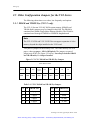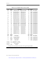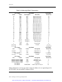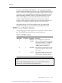
1
Artisan Technology Group is your source for quality
new and certified-used/pre-owned equipment
• FAST SHIPPING AND
DELIVERY
• TENS OF THOUSANDS OF
IN-STOCK ITEMS
• EQUIPMENT DEMOS
• HUNDREDS OF
MANUFACTURERS
SUPPORTED
• LEASING/MONTHLY
RENTALS
• ITAR CERTIFIED
SECURE ASSET SOLUTIONS
SERVICE CENTER REPAIRS
Experienced engineers and technicians on staff
at our full-service, in-house repair center
WE BUY USED EQUIPMENT
Sell your excess, underutilized, and idle used equipment
We also offer credit for buy-backs and trade-ins
www.artisantg.com/WeBuyEquipment
InstraView REMOTE INSPECTION
LOOKING FOR MORE INFORMATION?
Visit us on the web at www.artisantg.com for more
information on price quotations, drivers, technical
specifications, manuals, and documentation
SM
Remotely inspect equipment before purchasing with
our interactive website at www.instraview.com
Contact us: (888) 88-SOURCE | [email protected] | www.artisantg.com
VCL-V
and VCL-M
Graphics Boards User’s Manual
Rastergraf
Rastergraf, Inc.
1804-P SE First St.
Redmond, OR 97756
(541) 923-5530
FAX (541) 923-6575
web: http://www.rastergraf.com
email: [email protected]
Release 2.0
November 8, 2006
Artisan Technology Group - Quality Instrumentation ... Guaranteed | (888) 88-SOURCE | www.artisantg.com
Rastergraf
Artisan Technology Group - Quality Instrumentation ... Guaranteed | (888) 88-SOURCE | www.artisantg.com
Rastergraf
Table of Contents
INTRODUCTION.......................................................................................................... 1-1
THE ORGANIZATION OF THIS MANUAL ..................................................................................................... 1-1
GETTING HELP .......................................................................................................................................... 1-2
BOARD REVISIONS .................................................................................................................................... 1-2
NOTICES .................................................................................................................................................... 1-3
NOTICES .................................................................................................................................................... 1-3
MANUAL REVISIONS ................................................................................................................................. 1-3
CONVENTIONS USED IN THIS MANUAL ..................................................................................................... 1-4
CHAPTER 1 GENERAL INFORMATION ............................................................. 1-1
1.1
1.2
1.3
1.4
1.5
1.6
INTRODUCTION ................................................................................................................................... 1-1
FUNCTIONAL DESCRIPTION ................................................................................................................. 1-2
ADDITIONAL REFERENCES .................................................................................................................. 1-8
GENERAL SPECIFICATIONS FOR THE VCL SERIES ............................................................................... 1-9
MONITOR REQUIREMENTS ................................................................................................................ 1-17
CONFIGURATION INFORMATION ....................................................................................................... 1-18
CHAPTER 2 INSTALLING YOUR RASTERGRAF DISPLAY BOARD ........... 2-1
2.1 INTRODUCTION ................................................................................................................................... 2-1
2.2 UNPACKING YOUR BOARD ................................................................................................................. 2-2
2.3 VCL-V INSTALLATION ....................................................................................................................... 2-3
2.4 VCL-M INSTALLATION .................................................................................................................... 2-11
2.5 OTHER CONFIGURATION JUMPERS FOR THE VCL SERIES ................................................................. 2-16
2.6 CHECKING YOUR DISPLAY ................................................................................................................ 2-23
2.7 RS-232 CONNECTIONS TO THE VCL................................................................................................. 2-24
2.8 PS/2 CONNECTIONS .......................................................................................................................... 2-31
2.9 VIDEO CONNECTIONS TO THE VCL .................................................................................................. 2-35
2.10 HIGH SPEED DATA PORT (VCL-V ONLY)....................................................................................... 2-55
CHAPTER 3 SOFTWARE SUMMARY................................................................... 3-1
3.1 INTRODUCTION ................................................................................................................................... 3-1
3.2 SOFTWARE AVAILABILITY BY PLATFORM AND OS ............................................................................. 3-2
3.3 WRITE POSTING .................................................................................................................................. 3-3
3.4 PX WINDOWS SERVER ........................................................................................................................ 3-4
3.5 GRAPHICS SUBROUTINE PACKAGE...................................................................................................... 3-5
3.6 SMARTPTERM.................................................................................................................................... 3-9
3.7 SOFTWARE DEVELOPMENT PACKAGE................................................................................................ 3-10
CHAPTER 4 THEORY OF OPERATION............................................................... 4-1
4.1
4.2
4.3
4.4
4.5
4.6
4.7
4.8
INTRODUCTION ................................................................................................................................... 4-1
VCL-V SYSTEM DESIGN..................................................................................................................... 4-2
VCL-M SYSTEM DESIGN .................................................................................................................... 4-6
34020 FUNCTIONAL UNIT ................................................................................................................... 4-7
VCL CLOCKS ...................................................................................................................................... 4-9
DISPLAY MEMORY .............................................................................................................................. 4-9
SYSTEM MEMORY ............................................................................................................................. 4-11
PROGRAMMED LOGIC DEVICES ........................................................................................................ 4-11
Artisan Technology Group - Quality Instrumentation ... Guaranteed | (888) 88-SOURCE | www.artisantg.com
Rastergraf
CHAPTER 5 ON-BOARD DEVICES AND MEMORIES ...................................... 5-1
5.1 INTRODUCTION ................................................................................................................................... 5-1
5.2 VMEBUS (VCL-V) CONTROL REGISTERS ........................................................................................... 5-3
5.3 PCI BUS (VCL-M) CONTROL REGISTERS ......................................................................................... 5-10
5.4 LINE ADDRESS REGISTER (LAR) ...................................................................................................... 5-13
5.5 TMS 34020 GRAPHICS SYSTEMS PROCESSOR................................................................................... 5-17
5.6 INITIALIZATION TABLES ................................................................................................................... 5-31
5.7 GENERAL PURPOSE CONTROL REGISTER .......................................................................................... 5-43
5.8 RGB561 - COLOR MAP, CURSORS, AND PIXEL CLOCK ..................................................................... 5-46
5.9 SERIAL I/O PORTS ............................................................................................................................. 5-60
5.10 PC KEYBOARD/MOUSE CONTROLLER (8242PC) ............................................................................ 5-62
5.11 VCL-V HIGH SPEED DATA PORT (HSP)......................................................................................... 5-62
5.12 VCL INTERRUPTS ........................................................................................................................... 5-64
5.13 FLASH EEPROM AND SERIAL EEPROM ....................................................................................... 5-65
CHAPTER 6 TROUBLESHOOTING....................................................................... 6-1
6.1
6.2
6.3
6.4
6.5
6.5
6.6
INTRODUCTION ................................................................................................................................... 6-1
SELECTING AN ADDRESS RANGE FOR THE VCL-V BOARD ................................................................. 6-2
VCL-V MEMORY MAP EXAMPLE ....................................................................................................... 6-4
DOES THIS VCL-V BOARD TALK AT ALL? ........................................................................................... 6-5
GENERAL PROCEDURES ...................................................................................................................... 6-7
DEALING WITH THE PCI BUS .............................................................................................................. 6-9
MAINTENANCE, WARRANTY, AND SERVICE ..................................................................................... 6-10
Artisan Technology Group - Quality Instrumentation ... Guaranteed | (888) 88-SOURCE | www.artisantg.com
Rastergraf
Tables
Table 1-1 Common VCL-V Configurations ................................................................. 1-18
Table 1-2 Common VCL-M Configurations ................................................................ 1-18
Table 2-1 VMEbus graphics board addresses................................................................. 2-4
Table 2-2 CPU board addresses...................................................................................... 2-4
Table 2-3 Interrupt Grant Level...................................................................................... 2-6
Table 2-4 VCL-V DRAM and VRAM Size Jumpers................................................... 2-16
Table 2-5 PTERM Serial Control Options.................................................................... 2-19
Table 2-6 Default Initialization Table Selection Options ............................................. 2-20
Table 2-7 Initialization Table Selection Options .......................................................... 2-21
Table 2-8 Console Connector Pinout............................................................................ 2-26
Table 2-9 Jumpers for Console Port (Port 2) and Port 3 (VCL-V)............................... 2-26
Table 2-10 Jumpers for Console Port (Port 2) and Port 3 (VCL-M) ............................ 2-26
Table 2-11 Serial Mouse Connector Pinout.................................................................. 2-27
Table 2-12 Mouse Port (Port 0) and Port 1 (VCL-V)................................................... 2-28
Table 2-13 Mouse Port (Port 0) and Port 1 (VCL-M) .................................................. 2-28
Table 2-14 LK401 Connector Pinout............................................................................ 2-28
Table 2-15 VCL-M Serial Connector Pinout................................................................ 2-29
Table 2-16 MSE Cable Connections............................................................................. 2-30
Table 2-17 PS/2 Mouse Connector Pinout.................................................................... 2-32
Table 2-18 PC Keyboard Connector Pinout ................................................................. 2-32
Table 2-19 VCL-M Serial Connector Pinout................................................................ 2-33
Table 2-20 MKM Cable Connections........................................................................... 2-34
Table 2-21 VCL-M Video Connector Pinout ............................................................... 2-36
Table 2-22 MVI Cable Connections ............................................................................. 2-37
Table 2-23 VCL-M LVDS Digital Video Connector (J206) ........................................ 2-38
Table 2-23 Digital Output to LVDS Transmitter Conversion ...................................... 2-39
Table 2-24 Video Connector Pinout ............................................................................. 2-40
Table 2-26 How to Connect Unused Digital Input Lines ............................................. 2-43
Table 2-26 VCL Digital Video Connector (J206) ........................................................ 2-45
Table 2-27 NEC NL10276AC20-01 Connections........................................................ 2-46
Table 2-28 NEC NL12810AC20-04 Connections....................................................... 2-47
Table 2-29 Sharp LQ10DX01 Connections) ................................................................ 2-48
Table 2-30 Sharp LQ12D011 Connections) ................................................................. 2-49
Table 2-31 Sharp 640 x 480 Panels .............................................................................. 2-50
Table 2-32 Sharp EL Panel Model LJ64ZU48/9 ......................................................... 2-51
Table 2-33 Panel Side Connector Summary................................................................. 2-52
Table 2-34 Flat Panel Supplier Summary..................................................................... 2-53
Artisan Technology Group - Quality Instrumentation ... Guaranteed | (888) 88-SOURCE | www.artisantg.com
Rastergraf
Table 2-35 HSP VMEbus P2 Connector Pin Connections ........................................... 2-55
Table 3-1 Rastergraf Software and Operating Systems Support .................................... 3-2
Table 3-2 Graphics Subroutine Package Library Routines............................................. 3-6
Table 4-1 VCL-V VMEbus-side PLD Device Summary ............................................. 4-13
Table 4-2 VCL-M PCI/PMC-side PLD Device Summary ........................................... 4-13
Table 4-3 VCL-V and VCL-M 34020-side PLD Device Summary ............................. 4-14
Table 5-1 CSR Bit Summary .......................................................................................... 5-4
Table 5-2 CSR Bit Definitions........................................................................................ 5-5
Table 5-3 XARADR Address Match Register................................................................ 5-6
Table 5-4 DBRADR Address Match Register................................................................ 5-7
Table 5-5 Interrupt Vector Address Register.................................................................. 5-8
Table 5-5 VCL-M PLX9060 Serial EEPROM Listing................................................. 5-12
Table 5-6 LAR Bit Definitions ..................................................................................... 5-13
Table 5-7 VCL-V Side Device Buffer .......................................................................... 5-15
Table 5-8 VCL-M PCI bus Side Device Buffer............................................................ 5-16
Table 5-9 Byte/Word/Longword Mapping ................................................................... 5-21
Table 5-10 LAR/34020 Starting Address Table ........................................................... 5-24
Table 5-11 VCL-V Local Memory Map....................................................................... 5-27
Table 5-12 VCL-M Local Memory Map ...................................................................... 5-28
Table 5-13 34020 and VMEbus Register Offsets (VCLLAR = 400) ........................... 5-29
Table 5-14 34020 and PCI bus Register Offsets (VCLLAR = 400)............................. 5-30
Table 5-15 VCL Option Description ............................................................................ 5-31
Table 5-16 Summary of Initialization Tables ............................................................... 5-32
Table 5-17 Example Initialization Table (1280 x 1024, 110 MHz) ............................. 5-33
Table 5-18 General Purpose Control Register .............................................................. 5-43
Table 5-19 RGB561 registers ....................................................................................... 5-50
Table 5-20 RGB561 - VCL-V/24 Color Map Input Conversion.................................. 5-51
Table 5-21 RGB561 - VCL-x/8 Color Map Input Conversion..................................... 5-52
Table 5-22 Register Summary ...................................................................................... 5-57
Table 5-23 FIFO Control Register FCR0 Bit Assignments.......................................... 5-57
Table 5-24 FIFO Control Register FCR1 Bit Assignments.......................................... 5-58
Table 5-25 FIFO Control Register FCR2 Bit Assignments.......................................... 5-58
Table 5-26 DUART Control Bit Usage for HSP .......................................................... 5-63
Table 5-27 VMEbus Interrupt Functions...................................................................... 5-64
Table 5-28 34020 Interrupt Functions .......................................................................... 5-64
Table 6-1 Common CPU board addresses ...................................................................... 6-3
Table 6-2 Curing General System Faults........................................................................ 6-8
Artisan Technology Group - Quality Instrumentation ... Guaranteed | (888) 88-SOURCE | www.artisantg.com
Rastergraf
Figures
Figure 2-1
Figure 2-2
Figure 2-3
Figure 2-4
Figure 2-5
Figure 2-6
Figure 2-7
Figure 3-1
Figure 4-1
Figure 4-2
CSR Address and Interrupt Grant Level Jumpers......................................... 2-5
Interrupt Priority Jumpers ............................................................................. 2-7
Jumper Locations for the VCL-V ............................................................... 2-10
Jumper Locations for the VCL-M............................................................... 2-15
VCL-V DRAM and VRAM Size Jumpers.................................................. 2-16
VCL-V PTERM Configuration Jumpers (JP401) ....................................... 2-19
VCL-M PTERM Configuration Jumpers (JP301) ...................................... 2-19
Software Development Flow....................................................................... 3-10
VCL-V Block Diagram ............................................................................... 4-16
VCL-M Block Diagram .............................................................................. 4-18
Artisan Technology Group - Quality Instrumentation ... Guaranteed | (888) 88-SOURCE | www.artisantg.com
Artisan Technology Group - Quality Instrumentation ... Guaranteed | (888) 88-SOURCE | www.artisantg.com
Introduction
This introductory chapter contains information about the organization of
this manual, how to get technical support, and the typographical
conventions used throughout the manual.
The Organization of This Manual
This manual provides information about how to configure, install, and
program the Rastergraf 34020-based graphics controllers. Products
covered include the VCL series of 8-bit and 24-bit graphics controllers for
VME and PMC (PCI Mezzanine Card) bus compatible computers. The
boards can be covered in one manual because their feature set is largely
the same, and, as a result, the software is nearly identical.
This manual is broken down into six chapters:
Chapter 1: Overview of the Rastergraf display boards
Chapter 2: Installing Rastergraf display boards
Chapter 3: Summary of Rastergraf's Software Products
Chapter 4: Theory of Operation
Chapter 5: Programming On-board Devices and Memories
Chapter 6: Troubleshooting
Chapter 1 provides interesting background material about Rastergraf
display boards. Understanding the information in the chapter, however, is
not essential for the hardware or software installation.
If you want to perform the installation as quickly as possible, start with
Chapter 2. If you have problems installing the hardware, refer to Chapter 6
for help.
Artisan Technology Group - Quality Instrumentation ... Guaranteed | (888) 88-SOURCE | www.artisantg.com
Rastergraf
Getting Help
This installation manual gives specific steps to take to install your
Rastergraf display board. There are, however, variables specific to your
computer configuration and monitor that this manual cannot address.
Normally, the default values given in this manual will work. If you have
trouble installing or configuring your system, first read Chapter 6,
"Troubleshooting". If this information does not enable you to solve your
problems, do one of the following:
1)
call Rastergraf technical support at (541) 923-5530,
2)
fax your questions to (5410) 923-6475,
3)
or send E-mail to [email protected].
If your problem is monitor related, Rastergraf technical support will need
detailed information about your monitor.
Board Revisions
This manual applies to the following board revision levels:
VCL-V Fab Rev 2, 3
VCL-M Fab Rev 0, 1
Introduction-2
Artisan Technology Group - Quality Instrumentation ... Guaranteed | (888) 88-SOURCE | www.artisantg.com
Rastergraf
Notices
Information contained in this manual is disclosed in confidence and may
not be duplicated in full or in part by any person without prior approval of
Rastergraf, Inc. Its sole purpose is to provide the user with adequately
detailed documentation to effectively install and operate the equipment
supplied. The use of this document for any other purpose is specifically
prohibited.
The information in this document is subject to change without notice. The
specifications of the VCL-V and VCL-M and other components described
in this manual are subject to change without notice. Although it regrets
them, Rastergraf, Inc. assumes no responsibility for any errors or
omissions that may occur in this manual.
Rastergraf, Inc. assumes no responsibility for the use or reliability of
software or hardware that is not supplied by Rastergraf, or which has not
been installed in accordance with this manual.
Trademarks mentioned in this manual are the property of their respective
owners.
The VCL-V and VCL-M are manufactured and sold under license from
Curtiss-Wright Controls Embedded Computing. Contact Rastergraf, Inc.
for additional information.
Copyright © 2006 by Rastergraf, Inc.
Manual Revisions
Revision 1.0 October 17, 1997
Master cloned from VCL-V Manual.
Text altered and expanded to include
the VCL-P and the VCL-M.
Revision 1.1 January 26, 1998
Revisions and cleanup.
Revision 1.2 February 9, 1998
More revisions and cleanup. First full
customer release.
Revision 2.0 October 21, 2006
Delete the VCL-P. Convert from
Peritek names to Rastergraf.
Introduction - 3
Artisan Technology Group - Quality Instrumentation ... Guaranteed | (888) 88-SOURCE | www.artisantg.com
Rastergraf
Conventions Used In This Manual
The following list summarizes the conventions used throughout this
manual.
Code
fragments
Code fragments, file, directory or path names and
user/computer dialogs in the manual are presented in the
courier typeface.
Commands or
program names
Commands, or the names of executable programs, except
those in code fragments, are in bold.
System prompts
and commands
Commands in code fragments are preceded by the system
prompt, a percentage sign (%), the standard prompt in
UNIX's C shell, a dollar sign ($), the OS-9 prompt, or the
hash-mark (#), the standard UNIX prompt for the Super-User.
Note
Note boxes contain information either specific to one or more
platforms, or interesting, background information that is not
essential to the installation.
Caution
Caution boxes warn you about actions that can cause damage
to your computer or its software.
Warning!
Warning! boxes warn you about actions that can cause bodily
or emotional harm.
Keyboard usage
<CR> stands for the key on your keyboard labeled
“RETURN” or “ENTER”
Introduction-4
Artisan Technology Group - Quality Instrumentation ... Guaranteed | (888) 88-SOURCE | www.artisantg.com
Chapter 1
General Information
1.1 Introduction
This chapter provides an overview of the VCL series 8-bit and 24-bit
graphics controllers. Additional sections contain a bibliography,
specifications, monitor requirements, and common configurations.
This is summary information, and is not critical to the one who wishes to
press on to the installation procedures, which are contained in Chapter 2.
Artisan Technology Group - Quality Instrumentation ... Guaranteed | (888) 88-SOURCE | www.artisantg.com
Rastergraf
1.2 Functional Description
The Rastergraf VCL series boards are based on the TMS 34020 32-bit
Graphics System Processor (GSP). The boards offer a high degree of onboard intelligence and functionality, as well as a straightforward frame
buffer interface.
The boards are differentiated chiefly by the bits/pixel of the primary
display memory and by bus support. For example, the VCL-V/8 has 8
bits/pixel in the primary plane and the VCL-V/24 has 24-bits. Both
versions have analog and digital outputs. The VCL-M (PMC version) is
available only in 8-bit/pixel only, so its full model name is VCL-M/8.
The PX Windows and Graphics Subroutine Package software are bus
independent, enabling a user to easily switch between different bus
versions of the VCL.
The feature set of the VCL includes:
●
●
●
●
●
●
●
●
●
●
●
●
●
●
●
●
●
●
●
●
●
●
40 MHz 34020 Graphics Processor
34082 Floating Point Unit (FPU) option (VCL-V only)
RS-232 serial I/O ports and 2 PC (PS/2) compatible ports
4 Kb serial EEPROM plus up to 2 MB autoboot Flash PROM
Up to 32 MB 34020 memory on a single SIMM
Better than 1600 x 1280 displayable analog resolution
Up to 1280 x 1024 displayable digital resolution
LVDS compatible digital output (VCL-M/8 only)
8 bit overlay
Static overlay/repositionable primary display (or vice versa)
Optional multiple display pages
Hardware pan, zoom, and scroll and bitmapped cursors
PLL controlled pixel clock
Genlock option for system wide synchronization (VCL-V only)
Non-interlaced, interlaced (NTSC/PAL), and high refresh rate displays
Optional 32-bit High Speed Data port (VCL-V only)
Optional autoboot console terminal emulator
Low power BiCMOS bus transceivers and Lattice MACH FPGAs
Single 6U VMEbus board or PMC single-wide module
Ruggedized version available
Graphics Subroutine Package
X11R6 X Window System Server
General Information 1-2
Artisan Technology Group - Quality Instrumentation ... Guaranteed | (888) 88-SOURCE | www.artisantg.com
Rastergraf
TMS 34020 Graphics Processor
The TMS 34020 is a CMOS 32-bit processor with hardware support for
graphics operations such as PIXBLT and curve-drawing algorithms.
Included is a complete set of general purpose instructions with addressing
modes tuned to high level languages. In addition to addressing a 512 MB
external memory range, the 34020 contains 30 general purpose 32-bit
registers, stack pointer, and a 512 byte LRU instruction cache. On chip
functions include 64 programmable registers used for CRT timing, I/O
control, and instruction parameters. The 34020 can receive interrupts from
the the host bus and from serial I/O.
The 34020 mediates all host accesses to display and processor memory
and control registers through a byte addressable 32 bit interface port. Bus
transceivers between the 34020 bus and host (VME or PMC) bus support
single and burst 16 and 32 bit data transfers.
The 34020 features single-cycle execution of general purpose instructions
and most common integer arithmetic and Boolean operations from
instruction cache. A 32-bit barrel shifter supports single cycle shift and
rotation for 1 to 32 bits.
The 34020 graphics processing hardware supports pixel and pixel-array
processing. It incorporates two and three operand raster operations with
Boolean and arithmetic operations, XY addressing, window clipping and
checking, 1 to n bits/pixel transforms, transparency, and plane masking.
Operations on single pixels (PIXT instruction) or two-dimensional arrays
(PIXBLT) are supported.
TMS 34082 Floating Point Coprocessor (VCL-V only)
For floating point intensive applications, a socket is provided on the VCLV for a 34082 FPU coprocessor (due to space constraints, the FPU is not
available for the VCL-M). The 34082 conforms to the IEEE floating point
standard 754-1985 for binary floating point single or double precision
addition, subtraction, multiplication, division, square root, and
comparison. In addition, it offers 32-bit integer arithmetic, logical
comparisons, and shifts.
Complex operations for graphics support include: matrix operations (1 x 3,
3 x 3, 1 x 4, and 4 x 4), backface testing, polygon elimination and
clipping, viewport scaling and conversion, 2D and 3D linear interpolation,
2D window compare, 3D volume compare, 2 plane clipping (X, Y, Z), 2
plane color clipping (R, G, B, I), 2D and 3D cubic splines, 3 x 3
convolution, vector operations (add, subtract, dot and cross products,
1-3
General Information
Artisan Technology Group - Quality Instrumentation ... Guaranteed | (888) 88-SOURCE | www.artisantg.com
Rastergraf
magnitude, scaling, normalization and reflection), polynomial expansion,
multiply/accumulate, and 1D and 2D min/max.
Video RAM
The display memories use advanced 4 Mbit (256K x 16) 2-port Video
RAM (VRAM) technology, which gives approximately 95% memory
availability to the 34020 and host processors. A writemask register
supports write protection of bit planes.
The 34020 supports the VRAM accelerated functions such a block write
and fill with special VFILL and VBLT instructions. These can be used to
quickly replicate one and two dimensional patterns in memory, at up to 16
times the single pixel rate. Up to sixteen 8-bit pixels can be written in each
100 ns page mode cycle, resulting in a 160 Mpixel/sec VFILL time. With
the VCL-V/24, which use 32-bit pixels, you get up to 40 Mpixel/sec
VFILL time.
34020 Processor Memory (DRAM and EEPROM)
The 34020 has its own "system" memory, which is independent of the
video memory. However, it does share a common address space with the
display memory and can thus be used for program store or off-screen
display data. The standard size is 4 MB of 0-wait-state DRAM, and is
expandable to 32 MB.
There are four 32-pin IC locations which support up to 2 MB of 0 wait
state Flash EEPROM. Jumpers can be installed which cause the 34020 to
automatically start executing from PROM on power-up. An additional 512
byte serial EEPROM is installed which is used by Rastergraf's programs to
store information necessary at power-up (such as initialization data).
EEPROM sets can be ordered from Rastergraf which include a simple
console terminal emulator combined with the graphics subroutine package
and/or X11R6 X Windows server.
Display Features
The VCL contains a special function control part which allows the display
address for the overlay VRAM to be different from that of the primary
VRAM. This feature is used to support a "waterfall" display wherein a
static (non-moving) overlay status screen has an image in the primary
display memory which is scrolled or panned underneath it. Normally, the
alternatives are to: A, hardware scroll both overlay and primary and using
the 34020, software scroll back the overlay, or B, just software scroll the
primary. In either of these cases, the 34020 has to copy large amounts of
screen data which can result in limited scroll rates. In fact, a static
General Information 1-4
Artisan Technology Group - Quality Instrumentation ... Guaranteed | (888) 88-SOURCE | www.artisantg.com
Rastergraf
overlay/moving primary or moving overlay/static primary can be
supported.
Although not currently supported in Rastergraf software. the VCL can
provide binary vertical zoom (1, 2, 4, 8, 16, 32) and smooth horizontal
zoom.
The VCL display memory data is directed to the monitor via an IBM
RGB561 RAMDAC color map control chip which provides a
programmable 30 bit wide color map (10 bits each red, green, and blue).
The pixel is used as an index into the lookup table, giving 256 colors out
of a palette of 16.7 Million (2 * 24). The 24-bit VCL has a full 16.7
million color selection. A two bit cursor with a 64 x 64 x 2 bit map
function is also included on chip.
Additional color map entries are provided for the 8-bit overlay screen and
2-bit cursors. The analog output DACs are 10 bits per pixel. Additional
gamma correction lookup tables can be enabled to compensate for monitor
characteristics. The analog Red, Green, and Blue signals from the
RAMDAC are connected to a standard composite or VGA type analog
monitor.
The RGB561 also contains digital outputs which can be used to drive
LCD, plasma, or EL flat panel displays. Depending on how the VCL-V is
configured, 1, 4, or 8 bit monochrome or 8, 9, 12, 18, or 24 -bit color can
be supported. In all cases, the MSBs of the internal lookup tables are used.
The VCL-V 8-bit/pixel and 24-bit/pixel VCL drive the flat panel interface
using a direct TTL compatible interface. The VCL-M/8 uses an encoded
LVDS (Low Voltage Differential Signalling) protocol developed by
National Semiconductor and VESA. LVDS allows longer cable lengths
and is more noise tolerant.
Host Bus Interface
The VCL communicates with the VME or PMC host bus processor via a
host bus interface. Graphics board memory and on-board devices are
accessed through control registers and a 1 KB line buffer which are
located in VMEbus A16 space or PMC memory address space. The
VCL-V line buffer can also appear in A24 space.
The VCL-V differs with the VCL-M with respect to the implementation of
the control registers. The following sections detail these differences.
1-5
General Information
Artisan Technology Group - Quality Instrumentation ... Guaranteed | (888) 88-SOURCE | www.artisantg.com
Rastergraf
VCL-V Host Bus Interface
The VCL-V has a four word control register group: The CSR contains
device interrupt enables, line buffer response enable, and 34020 hardware
reset. The LAR is a 16 bit register which maps a portion of the address
space of the graphics board into the 1 KB line buffer. Two additional
registers include programmable line buffer address, interrupt vector
address and programmable extended address (A32) decoder. Access to the
board through the A16 space provides a "lowest common denominator"
access mode which allows the board to be compatible with any host CPU.
In an A16 VMEbus system it is necessary to "window" into on-board
memory because it is so large (maximum memory capacity on the board is
more than 48 MB!) The 1KB window is an efficient way of doing this.
The VCL-V also has a 64 MB window in A32 VMEbus address space
which allows direct access to all on-board memory.
VMEbus D32 block transfers are supported for A16/A24 and A32 address
spaces, which allows up to 256 bytes to be transferred at high speed over
the VMEbus. Another performance feature for the boards is a hardware
byte swapper. When enabled, four 1 KB buffers are mapped to the board
which provide unswapped, byte, word, and long swaps, respectively.
The board has a VMEbus interrupt controller which supports a vectored
interrupt from the 34020.
VCL-M Host Bus Interface
The VCL-M is designed to interface to a host processor which uses the
PCI bus. They use a PLX9060 PCI to Local Bus bridge to interface the
host processor to the 34020 host bus control. The 9060 contains PCI bus,
local bus, and on-chip DMA control registers. By necessity, therefore, the
software specific to setting up the control registers is different from the
VCL-V.
Device interrupt enables, line buffer response enable, 34020 hardware
reset, programmable line buffer address, interrupt vector address and
programmable extended address decoder bits are all contained in the 9060.
The LAR is a separately addressed 16 bit register which maps a portion of
the 34020 address space into the 1 KB line buffer window. Access to the
board through the 1K line buffer space provides a "lowest common
denominator" access mode which allows the board to be compatible with
any host CPU. In some PCI systems (even) it is necessary to "window"
into on-board memory because it is so large (maximum memory capacity
on the board is more than 48 MB!) The 1KB window is actually an
efficient way of doing this.
General Information 1-6
Artisan Technology Group - Quality Instrumentation ... Guaranteed | (888) 88-SOURCE | www.artisantg.com
Rastergraf
The graphics boards also have an 64 MB window which allows direct
access to all on-board memory.
The PLX9060 supports local chained DMA burst transfers between the
host and 34020 memory. Initial testing has shown that for Digital UNIX,
at least, there is no better than a 10% benefit to using DMA. Rastergraf
will evaluate DMA performance on other CPUs and OSs, and support
DMA in its software when and as it is appropriate. Please contact
Rastergraf engineering if you have questions about this.
Peripheral Support
The graphics board has four asynchronous RS-232 serial I/O ports.
Ordinarily, two ports are used to support serial mouse/trackball and
console (with RTS/CTS). The other two ports are not allocated. Each port
can be programmed separately for transmit and receive baud rates up to
38.4 Kb. Each receiver is quadruply buffered to minimize the possibility
of data overrun. Each channel has an internal loopback mode for testing.
The VCL-V uses two Philips SCN2681 DUARTs (Dual UART). The
VCL-M uses a single Philips SCC26C91 QUART (Quad UART).
An 8242PC controller provides PC-compatible keyboard and mouse ports.
PS/2 mini-DIN connectors are used.
The VCL-V (only) can be supplied with a 32-bit High Speed Port (HSP).
When connected to a compatible interface via the P2 VMEbus connector,
the 34020 can pass 32-bit data between the port and 34020 memory.
The Rastergraf graphics boards are highly configurable for special
requirements. In order to ensure optimum performance at the lowest OEM
cost, please contact Rastergraf for quotes for customized feature sets.
1-7
General Information
Artisan Technology Group - Quality Instrumentation ... Guaranteed | (888) 88-SOURCE | www.artisantg.com
Rastergraf
1.3 Additional References
Rastergraf documentation includes User's Manuals, Graphics Subroutine
Package Manual, and Rastergraf PX Windows Server Installation and
User's Guide. Data sheet extracts are available upon request. The
manufacturer sources of this information are:
TMS 34020 User's Guide
Order # SPVU019
Texas Instruments
Customer Response Center
1-800-232-3200
SCN2681AC1A44 Philips Semiconductors
Dual Asynchronous Receiver811 E. Arques Avenue
Transmitter (DUART) Data Sheet
Sunnyvale, CA 94088-3409
SC26C94C1A(800) 234-7381
Quad Asynchronous Receiver
Transmitter (QUART) Data Sheet
ICs for Data Communications Data Handbook
1992, pages 72-92 and 212-243
RGB561 Product Specification
#IOG561DSU-02 (Rev 1.1)
IBM Microelectronics
Route 100
Somers, NY 10589
1-800-IBM-0181
VME64 Specification
VITA
10229 N. Scottsdale Road
Suite B
Scottsdale, AZ 85253
(602) 951-8866
PCI Local Bus 2.1 Specification
PCI Special Interest Group
P.O. Box 14070
Portland, OR 97214
(800) 433-5177
Graphics Textbooks
Fundamentals of Interactive Computer Graphics
Addision Wesley, 1993.
Foley and Van Dam
Principles of Interactive Computer Graphics
McGraw-Hill, 1979
Newman and Sproull
General Information 1-8
Artisan Technology Group - Quality Instrumentation ... Guaranteed | (888) 88-SOURCE | www.artisantg.com
Rastergraf
1.4 General Specifications for the VCL Series
Graphics Processor:
40 MHz TMS 34020 Graphics System Processor has a
complete instruction set 32-bit CPU, vector and pix-blt
functions, and programmable video timing.
Floating Point Unit:
A socket is provided on the VCL-V board for the
companion 40 MHz TMS 34082 Floating-Point Unit (FPU)
coprocessor, which can accelerate floating-point intensive
operations by an order of magnitude. Due to space
limitations, the FPU is not available for the VCL-M.
Non-Display Memory:
Memory is 4 MB of 32-bits/word, byte addressable, nowait state, dynamic RAM. This memory is in the same
memory space as the display memory, so it can hold
program store and off screen display data. It is expandable
in steps of 4, 16 and 32 MB. A 72-pin SIMM is used. A
minimum of 4 MB is required for PX Windows.
EEPROM Memory:
Four 8-bit Flash EEPROMs support 1 wait state firmware
storage of up to 2 MB (total) of 32-bit wide permanent
storage. A user jumper allows any VCL to auto-start from
EEPROM.
A 4 Kbit (512 byte) serial Electrically Eraseable
Programmable Read Only Memory (EEPROM),
programmed via DUART (or QUART) control lines,
supplies non-volatile read-mostly memory for an EPROMbased application to retain some changeable data during
power down.
Video Display:
The IBM RGB561 lookup table (LUT) resolves the display
priority between the primary, overlay, and cursor (last
through first, respectively) screens.
On the 8-bit VCL (e.g. VCL-V/8), both the primary and
overlay word size is 32 bits, and there is 1 byte per pixel.
On the 24-bit VCL (e.g. VCL-V/24, the word size and pixel
size are both 32 bits. Bits 0-7 are Red, bits 8-15 are green,
bits 16-23 are blue, and bits 24-31 are overlay.
1-9
General Information
Artisan Technology Group - Quality Instrumentation ... Guaranteed | (888) 88-SOURCE | www.artisantg.com
Rastergraf
Pixel Clock:
The RGB561 RAMDAC contains a programmable pixel
clock generator. This allows the pixel clock to be set to
vitually any frequency between 5 and 170 MHz. The upper
range can be extended to 220 MHz by special order.
VCL 8 bit Display Memory: The basic display memory size for the 8-bit VCL is 1024 x
1024 8-bit pixels of 32-bits/word, byte addressable, no-wait
state, dual-port VRAM. Most configurations include both
primary and overlay displays. The display memory is
expandable: the /2M option can give either 1280 x 1024
displayable or two pages of 1024 x 1024 pixels. The /4M
option can give one page of 1600 x 1280, two pages of
1280 x 1024, or four pages of 1024 x 1024 pixels. The /8M
option can give two pages of 1600 x 1280, four pages of
1280 x 1024 or eight pages of 1024 x 1024.
VCL 24 bit Display Memory: The standard memory size for the 24-bit VCL is 2048 x
1024 32-bit pixels of 32-bits/word, byte addressable, nowait state, dual-port VRAM. This typically provides a 1280
x 1024 display size. The display memory is expandable: the
/4M option can give one page of 1600 x 1280, two pages of
1280 x 1024 or four pages of 1024 x 1024.
Writemask Register:
A writemask register permits individual bits in display
memory to be write protected. This allows write operations
(as opposed to read-modify-write) on display memory.
Static Display:
The VCL contains a special function which allows the
overlay screen to remain stationary while the primary
screen is moved (by changing the 34020's display start
address). Alternatively, the overlay can move and the
primary can be static. Normally, the 34020 would have to
copy the whole screen from one place to another to
accomplish this effect, which can lead to poor performance
for large screens.
Scroll, Pan, and Zoom:
Scroll - single line (smooth scroll).
Pan - anywhere on 4 pixel boundaries
Zoom: vertical (1, 2, 4, 8, 16, 32)
horizontal: sub-integer, uses the RGB561
PLL to adjust master pixel clock.
General Information 1-10
Artisan Technology Group - Quality Instrumentation ... Guaranteed | (888) 88-SOURCE | www.artisantg.com
Rastergraf
Color Map:
The VCL output uses an IBM RGB561 connected in basic
4:1 mux mode. It supports interlaced and non-interlaced
displays ranging from 640 x 480 up to better than 1600 x
1280. The RGB561 has a 64 x 64 x 2 bitmapped cursor and
a Gamma correction LUT. The DAC outputs are 10-bits.
Both analog and digital outputs are supported.
Digital Output Features:
The digital output is limited to 1280 x 1024 maximum. The
digital output resolution can be programmed to be 1, 4, 8,
9, 12, 18, or 24 bits per pixel.
Dual pixel output mode, required for 1024 x 768 and above
is supported. In this mode, pixel width is limited to 12 bits
(4 bits each Red, Green, Blue).
The VCL-M features the LVDS high speed encoded digital
interface. The LVDS port supports longer cable length and
reduced noise sensitivity.
Serial I/O Ports:
Four asynchronous serial I/O ports are contained in either
two Philips SCN2681 DUARTs or SC26C94 QUART.
Each port can be programmed for transmit and receive
baud rates up to 38.4 Kb. Receive buffers are quadruply
buffered to minimize the possibility of data overrun. The
DUARTs contain one programmable timer/counter and the
QUART has two. Ordinarily, one port is for a serial mouse
and one port is for the console (PTERM). RTS/CTS for the
console port is also included. Two ports are not assigned.
PS/2 Compatible Ports:
An Intel 8242PC controller supports 2 standard PC (PS/2)
ports. They can be used for PS/2 compatible mice and
keyboards (PTERM and PX Windows software support
available). Connection is made via a mini-DIN PS/2
connectors, or, on the VCL-M, via a micro-D-SUB..
Fuse Elements:
All voltages supplied to the serial and digital connectors are
protected either by current limiting resistors or resettable
fuses. The fuse is actually a Positive Temperature
Coefficient (PTC) resistor. It resets automatically when the
overload is removed.
1-11
General Information
Artisan Technology Group - Quality Instrumentation ... Guaranteed | (888) 88-SOURCE | www.artisantg.com
Rastergraf
1.4.1 Specifications for the VCL-V
VCL-V VMEbus Access: All VCL-V on-board registers are accessible to the
VMEbus through a 1 KB Line Buffer in A16 I/O space
using the 16-bit Line Address Register (LAR). Best
performance results if the VMEbus address space supports
D32 transfers. The Line Buffer may be located in A24
space if the host CPU only supports A16/D16. Contact
Rastergraf if you need to use this mode.
A direct A32 address mapping gives a 64 MB window into
board memory. In general, Rastergraf software does not use
the A32 addressing feature.
The graphics board has a four register block in the A16
space which contains the Control Status Register (CSR),
Line Address Register (LAR), Line Buffer Address
Register, Extended Address Register, and Interrupt Vector
Address Register.
VMEbus Interrupts:
The 34020 can cause an interrupt to the VMEbus.
Bus Loading:
Two bus loads
Data Strobe to DTACK:
Times were measured using an HP1650A logic analyzer at
the VME P1 connector, using 1000 test cycles. The 34020
was halted. The host CPU was a Motorola MVME162. You
must add about 150 ns of VMEbus overhead to get the total
cycle time. The long maximum access time results from
access during a memory refresh cycle.
Using the 162's DMA controller running VMEbus long
word block transfers, we measured an average 18 MB/s
write data tranfer rate. The 34020 was set for host bus
block transfer mode and read prefetch disabled.
34020 arbitrated accesses:
Write: min:
140 ns
max:
1.2 us
average: 168 ns
Read: min:
420 ns
max:
2.0 us
average: 497 ns
Analog Video Connections: The VCL-V uses a 15-pin VGA style, with Red, Green
with Composite Sync, and Blue, separate horizontal and
vertical sync. The pixel clock can optionally be output.
Genlock is an option available on the VCL-V. It requires
HSYNC in and VSYNC in. Contact Rastergraf for details
regarding genlock operation.
General Information 1-12
Artisan Technology Group - Quality Instrumentation ... Guaranteed | (888) 88-SOURCE | www.artisantg.com
Rastergraf
Digital Video Connector:
A 68-pin mini-D ribbon type connector supplies TTL level
1, 4, 8, 9, 12, 18, or 24 bit digital, sync, blanking, and +5
to flat panel displays. A variety of monochrome and color
panels have been tested and qualified. Current limited,
sequenced +5 and +12 are also supplied. Contact Rastergraf
about information regarding panel compatibility.
Serial Connector:
DB-9 connectors are provided for the console and mouse
connectors. Secondary serial ports are included on each
channel (thereby giving a total of 4 serial ports). Fused +12
volts is provided on the mouse connector.
PS/2 Connectors:
7 pin Mini-DIN (PS/2) type connectors are provided for the
PC keyboard and PS/2 mouse peripherals. Fused +5 volts is
provided on the connectors.
High Speed Port (HSP):
On the VCL-V (only), a 32-bit port allows the 34020 to
connect to an external device and read data directly into
memory at page-mode speeds (100 ns per transfer). A
simple handshake interface is used to control the external
device. Special routines in the graphics subroutine package
support HSP transfers.
The HSP is connected via the VMEbus P2 connector, using
the VSB pinout for most signals. However, it is not VSB
compatible.
Module Size:
6U Eurocard, 233 mm x 160 mm.
Power Requirements:
+5V +/- 5%, 3.0 A typical.
Environment:
Temperature:
Humidity:
Ruggedization Option:
Although Rastergraf is not formally in the militarized
business, it does offer a "ruggedized" version of the VCLV. Commercial grade components are used. The board is
protected with a conformal coating. It is Miller Stephenson
MS-460A spray-on, and is MIL-I-46058C, Type SR and
MIL-T-152B compliant. All socketed devices, including
the DRAM SIMM and Flash, are soldered in place. The
board is tested under extended temperature conditions:
Temperature:
1-13
0 to 70 degrees C, operating
-55 to +85 degrees C, storage
10% to 90%, non-condensing
-40 to 85 degrees C, operating
-55 to +85 degrees C, storage
General Information
Artisan Technology Group - Quality Instrumentation ... Guaranteed | (888) 88-SOURCE | www.artisantg.com
Rastergraf
1.4.2 Specifications for the VCL-M
VRAM Memory Options:
The small size of the VCL-M limits the choice of display
memory (VRAM), relative to the VCL-V. In fact, the
VCL-M is built in only one standard configuration, which
is with 4 MB of VRAM. It is normally allocated as 2 MB
for primary and 2 MB for overlay. This is sufficient for
1280 x 1024 displays,
Using a special initialization table , the VCL-M can be set
to 1600 x 1200, but due to intrinsic timing overhead, there
is a loss of about 25% in performance for certain graphics
drawing functions.
Alternatively, the VRAM can be allocated to serve as 4 MB
of primary display (no overlay) memory. In this case, you
can have the 1600 x 1200 at no loss of performance. or
have double-buffered (primary only) 1280 x 1024.
DRAM Memory Options:
In the case of DRAM, there are two choices of DRAM size:
16 MB and 32 MB. Unless you are using 1600 x 1200 or
have a lot of pixmaps, 16 MB is usually sufficient.
PCI bus Access:
All VCL-M on-board registers are accessible to the PCI bus
through a PLX9060 PCI to Local Bus Bridge. The 9060
provides programmable address and control registers which
map the 9060's PCI bus related registers and also the
VCL-M's CSR bits, Line Address Register (LAR), and 1
KB Line Buffer functions.
A secondary address mapping supported by the 9060 gives
a 64 MB window into board memory. This feature is useful
for applications which require direct, full frame buffer
access. Note that Rastergraf standard software products do
not use this feature.
On-Board DMA:
The 9060 has two complete on-chip DMA controllers.
They are capable of chain-loading, which means that
scatter-gather mapping can be supported. Initial testing
indicates that unless the transfer block is in excess of a few
KB, the CPU overhead doesn't make DMA worth the
effort..
PCI bus Interrupts:
Both 9060 local DMA controller and the 34020 can cause
an interrupt to the PCI bus.
Bus Loading:
One PCI 2.1 compatible load
General Information 1-14
Artisan Technology Group - Quality Instrumentation ... Guaranteed | (888) 88-SOURCE | www.artisantg.com
Rastergraf
Performance:
Times were measured using an HP1650A logic analyzer at
the PCI connector, using 1000 test cycles. The 34020 was
halted. The host CPU was a Digital 21066 Alpha
AXPpci33 computer.
Using the on-board 9060's DMA controller running 32-bit
block transfers, we have measured an average 18 MB/s
write data tranfer rate across the PCI bus. The 34020 was
set for host bus block transfer mode and read prefetch
disabled. The 34020 is the limiting factor in the bus transfer
speed, and the theoretical maximum is 20 MB/s.
Omitted Features:
The small size of the PMC board outline required the
omission of several secondary features available in the
VCL-V. These include: TMS34082 Floating Point
coprocessor, genlock, 24-bit (true color) version,
SIMM DRAM, and High Speed Port (for digital data
input).
The digital output port is different, as it uses LVDS
instead of standard TTL format to reduce pin count.
Analog Video Connections: The VCL-M uses a 9-pin MDSM micro D-Sub connector
to supply Red, Green with Composite Sync, Blue, and TTL
level horizontal and vertical sync. An adapter cable is
required to allow connection to a VGA or BNC compatible
monitor.
Digital Video Connector:
Digital video is encoded into LVDS (Low Voltage
Differential Signalling) compatible data. Each of the five
LVDS differential pairs carries seven digital video (TTL)
lines. A separate pair carries the PLL clock for the LVDS
system. LVDS allows much longer data cables and reduces
emitted noise.
A twenty pin .050" header is located near the front panel
which can connect to an off-board LVDS micro D ribbon
connector. Contact Rastergraf about information regarding
panel compatibility and LVDS interfacing.
Serial I/O Connector:
1-15
A 15-pin MDSM micro D-Sub connects the four serial
channels via a breakout cable to two offboard DB-9
connectors. The ports are used (nominally) for the console,
mouse, trackball, and serial keyboard.. Ordinarily, the serial
keyboard RS-232 lines are used for RTS/CTS for the
console port. In this case, then, you only have 3 ports.
Fused +12 volts is provided on the mouse connector.
General Information
Artisan Technology Group - Quality Instrumentation ... Guaranteed | (888) 88-SOURCE | www.artisantg.com
Rastergraf
PS/2 Connector:
A 9-pin MDSM micro D-Sub connects via a breakout cable
to two 7 pin Mini-DIN (PS/2) type connectors . These are
provided for the PC keyboard and PS/2 mouse peripherals.
Fused +5 volts is provided on the connectors.
Module Size:
Standard IEEE 1386 PMC bus card, 149 mm x 74 mm.
Power Requirements:
+5V +/- 5%, 1.5 A typical.
Environment:
Temperature:
Humidity:
0 to 70 degrees C, operating
-55 to +85 degrees C, storage
10% to 90%, non-condensing
General Information 1-16
Artisan Technology Group - Quality Instrumentation ... Guaranteed | (888) 88-SOURCE | www.artisantg.com
Rastergraf
1.5 Monitor Requirements
Rastergraf graphics boards can be used with a wide variety of monitors.
For best performance a monitor should have the following features:
●
●
●
●
●
Color RGB with composite sync on green analog video input
Switchable Termination (for monitor loopthrough)
Height, pincushion, width, phase, and position controls
Autotracking horizontal and vertical synchronization
High bandwidth 70 MHz (640 x 480)
135 MHz (1280 x 1024)
180 MHz (1600 x 1280)
● Horizontal refresh rate - 32 KHz (640 x 480)
70 KHz (1280 x 1024)
90 KHz (1600 x 1280)
Note: A standard VGA type (multi-scan) monitor can be plugged directly
into a VCL-V or VCL-M's adapter cable.
VCL-V and VCL-M Standard Display Timing Specifications
Display
Format
Vertical
Refresh
Horizontal
Refresh
Pixel
Clock
640 x 480
1024 x 768
1024 x 1024
1280 x 1024
1280 x 1024
1600 x 1280
60 Hz
60 Hz
70 Hz
67 Hz
72 Hz
60 Hz
31.5 KHz
60 KHz
64 KHz
64 KHz
72 KHz
79 KHz
27 MHz
80 MHz
85 MHz
110 Mhz
125 MHz
170 MHz
See Table 5-14 for more initialization table information.
Composite Video Signal:
1 Volt peak to peak consisting of:
660 mV Reference White +
54 mV Reference Black +
286 mV Sync Level
1-17
General Information
Artisan Technology Group - Quality Instrumentation ... Guaranteed | (888) 88-SOURCE | www.artisantg.com
Rastergraf
1.6 Configuration Information
The basic graphics board includes:
●
●
●
●
●
●
●
●
40 MHz TMS 34020 Graphics Systems Processor,
hardware cursors,
hardware pan, scroll, and zoom
programmable pixel clock
hardware byte swapper (VCL-V)
4 RS-232 data leads only serial ports
2 PS/2 compatible ports
analog and digital video outputs
(digital is an option on the VCL-M)
● interrupts.
Everything else is controlled by the options. Please contact Rastergraf
and/or refer to the short form catalog for more information about
configurations and accessories. The following tables show some common
models.
Table 1-1 Common VCL-V Configurations
Overlay
Model
Memory
VCL-V/24/X16
yes
VCL-V/8/X10
yes
VCL-V/8/X12
yes
VCL-V/8/X16
yes
34082
(FPU)
yes
option
option
option
34020
Memory
32 MB
4 MB
16 MB
16 MB
X Windows
Display
Compatible
Format
yes
1600 x 1280
yes
1024 x 768
yes
1280 x 1024
yes
1600 x 1280
Pixel
Size
24 + 8
8+8
8+8
8+8
Table 1-2 Common VCL-M Configurations
Model
VCL-M/8/X12
VCL-M/8/X16
Overlay
Memory
yes
yes
34082
(FPU)
n/a
n/a
34020
Memory
16 MB
16 MB
X Windows
Display
Compatible
Format
yes
1280 x 1024
yes
1600 x 1280
Pixel
Size
8+8
8+8
Part number notes – see next page.
General Information 1-18
Artisan Technology Group - Quality Instrumentation ... Guaranteed | (888) 88-SOURCE | www.artisantg.com
Rastergraf
Part Number Options:
/Xn
implies at least 4 MB of DRAM
//X10 1280 x 1024 display (1024 x 1024 addressable)
/X12
1280 x 1024 display (2048 x 1024 addressable)
/X16
1600 x 1280 display (2048 x 2048 addressable)
/nSM 34020 system memory in megabytes, where n = 4, 16, or 32
Note: VCL-M is 16 MB or 32 MB only.
/2M
2 pages of 1024 x 1024 (2048 x 1024 addressable pixels) primary
and overlay (this is already part of an X12 version)
/4M
4 pages of 1024 x 1024 (2048 x 2048 addressable pixels) primary
and overlay (this is already part of an X16 version)
/8M
8 pages of 1024 x 1024 (2048 x 4096 addressable pixels) primary
and overlay (VCL-V/8 version only)
/FPU 40 MHz 34082 Floating Point Coprocessor. VCL-V ONLY.
/HSD Digital Output for VCL-M. Standard on VCL-V.
/HSP 32-bit digital input port on P2 connector for VCL-V (only).
1-19
General Information
Artisan Technology Group - Quality Instrumentation ... Guaranteed | (888) 88-SOURCE | www.artisantg.com
Artisan Technology Group - Quality Instrumentation ... Guaranteed | (888) 88-SOURCE | www.artisantg.com
Chapter 2
Installing Your Rastergraf
Display Board
2.1 Introduction
There are 2 steps involved in getting your Rastergraf display board to
work in your system:
·
Unpack and install the Rastergraf display board.
·
Install the software
This chapter shows you how to install the Rastergraf display board in your
computer. The PX Windows Manual and the Graphics Subroutine Package
Manual provide instructions on how to install the software.
Artisan Technology Group - Quality Instrumentation ... Guaranteed | (888) 88-SOURCE | www.artisantg.com
Rastergraf
2.2 Unpacking Your Board
When you unpack your board, inspect the contents to see if any damage
occurred in shipping. If there has been physical damage, file a claim with
the carrier at once and contact Rastergraf for information regarding repair
or replacement. Do not attempt to use damaged equipment.
Caution
Be careful not to remove the board from its antistatic bag until you are
ready to install it. It is preferable to wear a grounded wrist strap whenever
handling computer boards.
Some operating systems require that you reboot your system after
installing a device driver, because only after the reboot will your system
utilize the driver and recognize the board. If yours is such an operating
system, you might like to install PX Windows or the Subroutine Package
before installing the board since you will have to shut down the computer
to install the board anyway. If you want to install the software before
shutting down the computer, proceed to the correct part of the relevant
software manual and return to this chapter afterwards.
Recommendation:
The following sections tell how to install the VCL board and how to
change jumpers. In order to avoid unintended side-effects, it is best not to
change any jumpers (except critical address jumpers) until you are sure the
board works in your system.
Installing Your Rastergraf Display Board 2-2
Artisan Technology Group - Quality Instrumentation ... Guaranteed | (888) 88-SOURCE | www.artisantg.com
Rastergraf
2.3 VCL-V Installation
The VCL-V is designed to plug into any standard VME or VME64
backplanes. The VCL-V will work also correctly in a 5 row DIN
(VME64x) systems, as these connectors have the center 3 rows of
connections in common with the the VME64 backplane.
The VCL-V/24 and VCL-V/8 share virtually all jumper configurations.
They use the identical PC board. They differ only in their plug in parts
such as FPGAs and the VRAM memory module.
The following instructions tell how to modify the VCL-V FAB REV 2 and
REV 3 to a non-standard configuration. Refer to Figure 2-3 Jumper
Option Locations for VCL-V (at the end of this section) for jumper
locations. For wire-wrap changes, only KYNAR or TEFLON, not enamel
or plastic coated, insulated wire should be used.
2.3.1 Checking Board Addresses
Before installing the board in the backplane, you must confirm that the
addresses used by the Rastergraf display board are not used by other
devices in your computer. Since many boards are fully configured after the
operating system boots up, this may not be easy to do. Refer to the
Rastergraf PX Windows and Graphics Subroutine Package manuals for
more installation information.
The Rastergraf VMEbus graphics boards have three address ranges:
● Control Registers
● Line Buffer
● 64 MB Memory Window
Jumper programmable
Software Programmable
Software Programmable
Note
Only the multiprocessor version of the PX Windows server uses the 64MB memory window.
Before installing the board into your backplane, make sure no other
devices in your computer respond to Rastergraf's graphics board
addresses, listed in Table 2-1:
2-3
Installing Your Rastergraf Display Board
Artisan Technology Group - Quality Instrumentation ... Guaranteed | (888) 88-SOURCE | www.artisantg.com
Rastergraf
Table 2-1 VMEbus graphics board addresses
Standard Address
Address
Type
Data Type
Control Registers
xxxxC000-xxxxC00F
A16
D16, D32
Line Buffer
xxxxy000-xxxxy3FF
A16
D8, D16, D32
Full Memory
A0000000-A3FFFFFF
A32
D8, D16, D32
Interrupt Vector
E0
–
D8 interrupter
The xxxx is a placeholder for digits that are processor specific. Some
common values are shown in Table 2-2. Full memory settings are only
used in multiple Rastergraf board configurations. The y in the line buffer
address is a placeholder for a digit which is processor specific. These
addresses are the defaults used by Rastergraf. Only the Control Register
address is set by jumpers on the graphics board. The Line Buffer and Full
Memory addresses and the Interrupt Vector are software configurable.
The table below gives you values for xxxx and y for some common
CPUs.Consult Chapter 6 for information on determining addresses of
boards not shown in the table.
Table 2-2 CPU board addresses
Processor/Mfgr.
Value of xxxx
Value of y
Addressing Modes
Force 68K
FBFF
0
A16
Force SPARC
FBFF
0
A16/D32
Heurikon 68K
0100
8
A16
Motorola 68K,88K
FFFF
8
A16
Themis SPARC
FFFF
0
A16/D32
Sun, HP
0000
8
A16
Installing Your Rastergraf Display Board 2-4
Artisan Technology Group - Quality Instrumentation ... Guaranteed | (888) 88-SOURCE | www.artisantg.com
Rastergraf
2.3.2 CSR Address Jumpers
The address range for the CSR block is jumper selectable to certain
addresses in A16 space. As configured at the factory, bits 4, 5, 14, 15 are
used in the address selection, bits 0-3 are used in the register selection, and
bits 6-13 are hardwired low. If required, bits 6-13 can be some other
pattern - contact Rastergraf if you need this.
Remember that the base addresses for the Line Buffer, Extended Address
Block, and Interrupt Vector are all software programmable. Furthermore,
if you select the Alternate group 12-15, you will conflict with the standard
Line Buffer address (FFFF0000-FFFF03FF) used by Rastergraf software
for the Line Buffer. Section 5.2 has complete information about
programming these registers. Refer also to Chapter 6 and note the
comments concerning use of the Motorola MVME167 and
MVME187.
Figure 2-1 CSR Address and Interrupt Grant Level Jumpers
8-pin resistor pack
GND
GND
GND
GND
GND
GND
GND
A15
A14
A5
A4
VS2
VS1
VS0
Address Selection
VMEbus (Hex)
default jumpers
Standard
Alternate 1
Alternate 2
Alternate 3
Alternate 4-7
Alternate 8-11
Alternate 12-15
xxxxC000-xxxxC00F
xxxxC010-xxxxC01F
xxxxC020-xxxxC02F
xxxxC030-xxxxC03F
xxxx80n0-xxxx80nF
xxxx40n0-xxxx40nF
xxxx00n0-xxxx00nF
A4, A5 installed
A5 installed
A4 installed
-A14, A5, A4
A15, A5, A4
A14, A15, A5, A4
Note: xxxx depends on host processor's A16 VMEbus address space.
2-5
Installing Your Rastergraf Display Board
Artisan Technology Group - Quality Instrumentation ... Guaranteed | (888) 88-SOURCE | www.artisantg.com
Rastergraf
2.3.3 Interrupt Grant and Priority Jumpers
Rastergraf boards are normally configured for interrupt level 3 (IRQ3). If
you change this setting, the device driver needs to be changed accordingly.
Rastergraf boards have a programmable interrupt vector address, which is
usually set by the software to default to E0 (hex). However, some
platforms, such as Sun, permit the vector to be chosen transparently by the
operating system. In these cases, you do not need to specify an interrupt
vector address.
Make sure that any boards which do not use interrupts have their interrupt
pass-grant jumper installed. Conversely, remove the jumpers for all boards
that use interrupts. Finally, make sure you install the jumper in slot 0
IACK to IACKIN. Don't confuse this jumper with the
IACKIN/IACKOUT jumper. On many backplanes, slot 0 IACK to
IACKIN does not have a removable jumper; IACK is always connected to
slot 0 IACKIN.
The VMEbus has a seven level interrupt grant receive/acknowledge
protocol which requires each board to acknowledge that it is responding to
the interrupt grant level that it requested. Three jumpers set this response
level. Refer to the Jumper Location Figure for the VCL-V (above) for the
location of the jumpers. In the table below, 0 equals jumper installed.
Table 2-3 Interrupt Grant Level
Grant Level
1
2
3
4
5
6
7
VS Jumper Number
2
1
0
0
0
1
0
1
0
0
1
1
1
0
0
1
0
1
1
1
0
1
1
1
Default
yes
The VMEbus interrupt request priority is jumper programmable for the
seven levels (1-7). The lower the priority number the less likely the board
will be serviced. The Interrupt Request Priority jumper block the left side
of J1 (VME P1 connector. The pin layout is as follows:
Installing Your Rastergraf Display Board 2-6
Artisan Technology Group - Quality Instrumentation ... Guaranteed | (888) 88-SOURCE | www.artisantg.com
Rastergraf
Caution
The Vector Priority setting must match the Interrupt Request Priority
setting.
Figure 2-2 Interrupt Priority Jumpers
IRQ7
IRQ3
IRQ6
IRQ2
IRQ5
IRQ1
IRQ4
IRQ
J1
2.3.4 Installing the VCL-V Graphics Board
Review Section 2.5, Other Jumper Options for the VCL Series, for other
jumpers which you may need to change.
Use the following procedure to install the Rastergraf display board into the
VMEbus backplane.
1. Shut down the operating system and turn off the power.
Warning!
Never open the computer without turning off the power supply. Unless
internal AC wiring is exposed, leave the power cord plugged in, so as to
ground the computer chassis. You can easily get shocked, ruin computer
parts or both unless you turn off the power. Even with power switched off,
lethal voltages can exist in the equipment.
2. Open the computer and identify the empty slot in the card cage that is
closest to the CPU. Do not leave any slots empty between the graphics
board and the CPU.
2-7
Installing Your Rastergraf Display Board
Artisan Technology Group - Quality Instrumentation ... Guaranteed | (888) 88-SOURCE | www.artisantg.com
Rastergraf
Note
There must not be any open slots between the first and last boards which
use either DMA or interrupts (this includes the Rastergraf display board,
which uses interrupts).
3. Remove the interrupt pass/grant from the board slot.
The shorting jumper for Slot 2 IAKIN/OUT should be removed
(assuming the VCL-V is to be installed in that slot). Shorting jumpers
should be installed for all unused slots
The jumper may be on the front or back of the backplane. Some
backplanes don't have jumpers to remove. The jumper is an integral
part of the slot in such cases. It is activated automatically when the
card is inserted.
4. Wear a grounded wrist strap. Touch a metal part of the computer
chassis, remove the graphics board from its anti static bag, and
immediately slide it into the slot.
Caution
The static electricity that your body builds up normally can seriously
damage the integrated circuits on the graphics board. You should first
touch the metal part of the chassis, which will short circuit the static
charge on your body to ground. It is preferable to wear a grounded wrist
strap whenever handling computer boards.
Handle the graphics board only by its edges. Oils from your hand can
break down the metal used in the circuit board.
5. After making sure the board is seated correctly, tighten the screwlock
on each end of the board.
6. Close the computer and plug the video cable into the monitor and the
graphics board. Make sure to plug the three BNC cables, colored red,
green, and blue, into the monitor's corresponding red, green, and blue
inputs. Also, make sure the 75 ohm switch on the monitor is turned on.
VGA monitors which use a 5-wire cable (which can be obtained on
special order), may also require modified initialization tables.
Installing Your Rastergraf Display Board 2-8
Artisan Technology Group - Quality Instrumentation ... Guaranteed | (888) 88-SOURCE | www.artisantg.com
Rastergraf
2.3.5 Connecting the Mouse, Keyboard, and Console
If you are not using a keyboard or other I/O device, just skip on to Section
2.6 Checking your Display.
PS/2 Mouse and Keyboard Ports
Plug a PS/2 compatible mouse cable into the PS/2 connector (round 6-pin
DIN socket) labeled PS/2 MOUSE.
Plug a PC-AT compatible keyboard with a PS/2 style connector or adapter
into the round DIN 6-pin socket labeled PC KBD.
RS-232 Serial Ports
Plug an RS-232 serial mouse cable into the 9-pin DB-9 male connector
labeled MOUSE. You can also use a trackball in this port.
If you are using the PTERM terminal emulator, plug the console cable
from the computer into the 9-pin female connector labeled CONSOLE.
PTERM supports 9600 baud. Jumpers control the data bits, parity, and
RTS/CTS and XON/XOFF protocol. See Section 2.7. The console port of
your computer should match the VCL-M settings. If you have trouble,
refer to Chapter 6 or contact Rastergraf.
2-9
Installing Your Rastergraf Display Board
Artisan Technology Group - Quality Instrumentation ... Guaranteed | (888) 88-SOURCE | www.artisantg.com
Rastergraf
Figure 2-3 Jumper Locations for the VCL-V
34082 (FPU)
Socket
(optional)
Sections
2.6.1, 2.6.4
& 2.6.6
Section
2.6.2
JP301
JP402
Flash
EEPROM
Sockets
BOOT
Pin 1
J404
PS/2
MS
Byte 0
JP407
JP409
Sections
2.3.2 & 2.3.3
Byte 2
Pin IRQ
Jumper A
Section
2.3.3
JP101
J205
Video
Section
2.6.7
JP102
Byte 3
J402
Console
JP410
JP403
JP404
Byte 1
J401
Serial Mouse
JP405
JP408
J403
PC KB
Section
2.8.1
JP401
J206
Digital Video Out
Installing Your Rastergraf Display Board 2-10
Artisan Technology Group - Quality Instrumentation ... Guaranteed | (888) 88-SOURCE | www.artisantg.com
Rastergraf
2.4 VCL-M Installation
The VCL-M is designed to plug into any IEEE 1386 compatible single
module PMC location. PMC locations are currently supported on VME
and CompactPCI compatible computers and PCI/PMC expander boards.
The VCL-M will work also correctly in a system where the base board is a
PCI motherboard. In this case, you use a Technobox 1586 PMC to PCI
adapter to enable plugging a PMC board (the VCL-M) into a PCI slot.
Although perhaps not suitable for a long term installation, it can be a
convenient thing to do.
The following instructions tell how to modify the VCL-M FAB REV 0
(and above) to a non-standard configuration. Refer to Figure 2-4 Jumper
Option Locations for VCL-M (at the end of this section) for jumper
locations. For wire-wrap changes, only KYNAR or TEFLON, not enamel
or plastic coated, insulated wire should be used.
2.4.1 Checking Board Addresses on the VCL-M
Since the PMC bus (actually, it is really a PCI bus) and the VCL-M are
configured by the operating system and/or BIOS while booting up, there
isn't any hardware to change for the addresses. Refer to the Rastergraf PX
Windows and Graphics Subroutine Package manuals for more
information.
The Rastergraf VCL-M uses registers in the PLX9060 PCI bus to local bus
bridge chip internal register set and also has address ranges outside the
PLX's (internal) address space which give access to the VCL-M's control
registers and memory blocks. The BAR (Base Address Register) sets in
the 9060 are programmed to point to these areas.
The Rastergraf VCL-M device driver loads these registers. And, if you can
determine the actual PCI base address, you should be able to probe the
address spaces with an on-line debugger once the driver code has run.
Section 5.3 has details on how the PLX9060 controls access to the onboard registers.
Since it is not intended for PC type applications, the VCL-M does not
support an x86 BIOS. However, Rastergraf does have autobooting PROM
sets for the VCL-M which will make it load and run Built In Self
Test/terminal emulator (SmartPTERM), PTERM (console emulator), PX
Windows server, or Graphics Subroutine Package programs in its onboard CPU. Contact Rastergraf for more information on these options.
2-11
Installing Your Rastergraf Display Board
Artisan Technology Group - Quality Instrumentation ... Guaranteed | (888) 88-SOURCE | www.artisantg.com
Rastergraf
You will notice that there isn't any good information supplied here which
will allow you to reliably probe the VCL-M addresses. That is because the
ability to do this is absolutely dependent on the CPU board memory map
as implemented by the system OS and the address ranges of the PCI bus as
determined by the CPU hardware. These things change from OS to OS,
board to board, and vendor to vendor, making this simple task a big pain.
Therefore, you have to work closely with your CPU board, the OS's BSP,
and collateral information supplied by Rastergraf and PLX to actually
touch the registers. Fortunately, if you install the PX Windows or
Graphics Subroutine software, the board will show up and you will get
pictures.
2.4.2 Default Interrupt Settings on the VCL-M
Rastergraf boards are configured for interrupt request INTA. Since each
PMC slot maps its interrupt lines to a permuted set of INTA-INTD, the
VCL-M will show up on a different interrupt line, according to the slot it
is plugged into. Therefore, the device driver needs to be changed
accordingly to reflect this. The VCL-M has a programmable interrupt
vector address, which is set by the Rastergraf device driver..
2.4.3 Installing the Graphics Board
Use the following procedure to install the VCL-M into the computer
1. Shut down the operating system and turn off the power.
Warning!
Never open the computer without turning off the power supply. Unless
internal AC wiring is exposed, leave the power cord plugged in, so as to
ground the computer chassis. You can easily get shocked, ruin computer
parts or both unless you turn off the power. Even with power switched off,
lethal voltages can exist in the equipment.
2. Open the computer and remove the CPU board onto which the VCL-M
is to be installed. Find identify an empty PMC location (typically,
there are, at most, two on a given CPU board. In the interest of
allowing air flow, and if you have a choice, try to install the VCL-M in
the location which allows the best airflow through card cage.
Installing Your Rastergraf Display Board 2-12
Artisan Technology Group - Quality Instrumentation ... Guaranteed | (888) 88-SOURCE | www.artisantg.com
Rastergraf
3. If you are using the digital video connector, you may need additional
panel space to mount it, since cable comes off the VCL-M and has to
be routed and installed elsewhere.
4. Wear a grounded wrist strap. Touch a metal part of the computer
chassis, remove the graphics board from its anti static bag, and
immediately slide it into the slot.
Caution
The static electricity that your body builds up normally can seriously
damage the integrated circuits on the graphics board. You should first
touch the metal part of the chassis, which will short circuit the static
charge on your body to ground. It is preferable to wear a grounded wrist
strap whenever handling computer boards.
Handle the graphics board only by its edges. Oils from your hand can
break down the metal used in the circuit board.
5. Remove the blocking plate from computer's front panel, and after
making sure the board is seated correctly, install the four mounting
screws (two near the front and two near the PMC connectors). In a
similar way, install any additional plate for the digital video port.
6. Close the computer and plug the video cable into the monitor and the
graphics board. Make sure to plug the three BNC cables, colored red,
green, and blue, into the monitor's corresponding red, green, and blue
inputs. If you are using a VGA to monitor 15-pin D-Sub cable, then, of
course, plug that end into monitor.
Also, make sure the 75 ohm switch on the monitor is turned on. VGA
monitors which use a 5-wire cable (which can be obtained on special
order), may also require modified initialization tables.
2-13
Installing Your Rastergraf Display Board
Artisan Technology Group - Quality Instrumentation ... Guaranteed | (888) 88-SOURCE | www.artisantg.com
Rastergraf
2.4.4 Connecting the Mouse, Keyboard, and Console
If you are not using a keyboard or other I/O device, just skip on to Section
2.6 Checking your Display.
PS/2 Mouse and Keyboard Ports
The PS/2 ports are available on a 9-pin MDSM micro D-sub. A breakout
cable available from Rastergraf provides the PS/2 connectors.
Plug a PS/2 compatible mouse cable into the PS/2 connector (round 6-pin
DIN socket) labeled PS/2 MOUSE.
Plug a PC-AT compatible keyboard with a PS/2 style connector or adapter
into the round DIN 6-pin socket labeled PC KBD.
RS-232 Serial Ports
The RS-232 serial ports are available on a 15-pin MDSM micro D-sub. A
breakout cable available from Rastergraf provides the 9-pin D-sub
connectors.
Plug an RS-232 serial mouse cable into the 9-pin DB-9 male connector
labeled MOUSE. You can also use a trackball in this port.
If you are using the PTERM terminal emulator, plug the console cable
from the computer into the 9-pin female connector labeled CONSOLE.
PTERM supports 9600 baud. Jumpers control the data bits, parity, and
RTS/CTS and XON/XOFF protocol. See Section 2.7 The console port of
your computer should match the VCL-M settings. If you have trouble,
refer to Chapter 6 or contact Rastergraf.
Installing Your Rastergraf Display Board 2-14
Artisan Technology Group - Quality Instrumentation ... Guaranteed | (888) 88-SOURCE | www.artisantg.com
Rastergraf
Figure 2-4 Jumper Locations for the VCL-M
DRAM
Lo Bank
DRAM
Lo Bank
DRAM
Hi Bank
J303
RS-232
Pin 1
J301
VIDEO
J304
J302
PC MS/KB
DRAM
Hi Bank
Section
2.8.1
Section
2.6.4
JP303
Green LED
JP301
Flash
Hi Word
Yellow LED
Red LED
Flash
Lo Word
BOOT
LVDS
Jumper A
Jumper B
Jumper C
Jumper D
Jumper E
Jumper F
Jumper G
Jumper H
Section
2.6.7
2-15
Installing Your Rastergraf Display Board
Artisan Technology Group - Quality Instrumentation ... Guaranteed | (888) 88-SOURCE | www.artisantg.com
Rastergraf
2.5 Other Configuration Jumpers for the VCL Series
The following subsections cover other, less frequently used options.
2.5.1 DRAM and VRAM Size (VCL-V only)
The VCL-V (but not VCL-M) 34020 system memory (DRAM) and
VRAM display memory may be changed in the field. The DRAM is
contained on a SIMM (Single Inline Memory Module). The VRAM is
contained on a Rastergraf VMEM8 or VMEM24 daughterboard.
Note
The VCL-V/8/X10 and VCL-V/8/X12 do not support expansion of video
memory beyond the chips installed on the VCL board.
Two pairs of jumpers set the memory sizes. The video memory size is in
pages, where one page = 1024 x 1024 pixels. The jumpers are part of
jumper strip JP301 (see Figure 2-5 below): Note that for both the DRAM
and VRAM tables, 0 = Jumper Installed
Figure 2-5 VCL-V DRAM and VRAM Size Jumpers
10 Pin Resistor Pack
BOOT
resv
resv
FORCE
OLAY
resv
D1
D0
V1
V0
GRD
GRD
GRD
GRD
GRD
GRD
GRD
GRD
GRD
Table 2-4 VCL-V DRAM and VRAM Size Jumpers
V1
V0
VRAM Size
D1
D0
DRAM Size
0
0
1 page
0
0
1 or 4 MB
0
1
2 pages
0
1
8 MB
1
0
4 pages
1
0
16 MB
1
1
8 pages
1
1
32 MB
Installing Your Rastergraf Display Board 2-16
Artisan Technology Group - Quality Instrumentation ... Guaranteed | (888) 88-SOURCE | www.artisantg.com
Rastergraf
2.5.2 Flash EEPROM for the VCL-V
The VCL-V requires four 32-pin PLCC Flash EEPROMS. Acceptable
devices include AM28F020-150JC (for 1 MB total) and AM29F040150JC (for 2 MB total). Access time must be less than 150nS. Install a
jumper between pins 1 and 2 of JP402 (see Figure 2-3) when using the
AM29F040 parts. Rastergraf has a program which is available upon
request which can be used to load images into the EEPROMs under
VxWorks and Solaris.
28F020 Program Voltage Enable
In order to program the 28F020 EEPROMs ONLY, a jumper to enable 12
Volts must be installed between pins 2 and 3 of JP402 (see Figure 2-3).
Caution
1) Remove the jumper once you are done programming.
2) DO NOT INSTALL JUMPER WHEN PROGRAMMING 29F040.
2.5.3 Flash EEPROM for the VCL-M
The VCL-M Flash is soldered onto the board, and is therefore not field
changeable. The Flash EEPROMS are either 2 Mbit AM28F400 (for 1 MB
total) or 4 Mbit AM29F800 (for 2 MB total) EEPROMs. Rastergraf has a
program which is available upon request which can be used to load images
into the EEPROMs under VxWorks and Solaris.
2-17
Installing Your Rastergraf Display Board
Artisan Technology Group - Quality Instrumentation ... Guaranteed | (888) 88-SOURCE | www.artisantg.com
Rastergraf
2.5.4 Autoboot Enable (all VCLs)
The VCL can start up from on-board Flash on power-up or anytime
SYSRESET is asserted. NOTE: to avoid unpredictable board operation,
do not install this jumper unless autobooting EEPROMS are installed.
To enable autoboot operation, install a jumper in the BOOT location of
JP301. See Figure 2-3 for the VCL-V or Figure 2-4 for the VCL-M.
2.5.5 Master Pixel Clock Oscillator Frequency (all VCLs)
The VCL boards have a software programmable pixel clock contained in
the IBM RGB561 RAMDAC which can be set up to 170 MHz. Rastergraf
distributes a number of standard initialization tables, and can provide
custom versions upon request. Using a specially upgraded VCL, the pixel
clock can be in excess of 250 MHz.
2.5.6 Force Overlay Jumper (all VCLs)
Actually, there is no FORCEOLAY jumper on the VCL-M, but you
should still read this section.
Background
You can configure the VCL display memory to have equal parts primary
and overlay or to be all primary. You might use the primary-only case if
you don't need overlay and you want as much primary memory as
possible. The effect of disabling overlay memory is to double the primary
memory. Thus, you can increase the display resolution, from, for example,
1024 x 768 to 1280 x 1024. So, you can run an /X10 board as an /X12, or
an /X12 as an /X16 board, as long as you don't need overlay.
Jumper Settings
If the jumper is installed, the OLAYDIS in the GPCR (see Table 5-19) is
overridden and overlay memory is forced on. The jumper prevents you
from programmably enabling overlay memory. Note: the VCL-M doesn't
have a FORCEOLAY jumper, so be careful about the OLAYDIS bit.
If the jumper is removed, then the OLAYDIS bit can be set under
program control. Setting the bit causes all memory to allocated to the
primary only, and overlay cannot be used.
Installing Your Rastergraf Display Board 2-18
Artisan Technology Group - Quality Instrumentation ... Guaranteed | (888) 88-SOURCE | www.artisantg.com
Rastergraf
2.5.7 Selecting PTERM Options (all VCLs)
Figure 2-6 VCL-V PTERM Configuration Jumpers (JP401)
J402
GRD
GRD
GRD
GRD
GRD
GRD
GRD
GRD
A
B
C
D
E
F
G
H
resv
Figure 2-7 VCL-M PTERM Configuration Jumpers (JP301)
GRD
GRD
GRD
GRD
GRD
GRD
GRD
GRD
GND
H
G
F
E
D
C
B
A
BOOT
The XON/XOFF flow control only applies to data being sent to PTERM.
However, PTERM has an input buffer which can handle bursts of up to
8KB without requiring XON/XOFF flow control.
The RTS/CTS flow control is done by programming the UART to enable
auto-control of the RTS/CTS lines. It is unlikely that the CTS signal will
be asserted because the 34020 should be able to service UART interrupts
prior to the next character being received. The RTS signal will control
output from PTERM to the host.
Note:
If RTS is enabled but not connected, PTERM will not transmit to the host.
Table 2-5 PTERM Serial Control Options
2-19
Jumper
Function
Open
Shorted
A
B
C
serial mode
XON/XOFF
RTS/CTS
8 bits/No parity
disabled
disabled
7 bits/Even parity
enabled
enabled
Installing Your Rastergraf Display Board
Artisan Technology Group - Quality Instrumentation ... Guaranteed | (888) 88-SOURCE | www.artisantg.com
Rastergraf
Initialization Tables in PTERM
The PTERM flash EEPROM contains 4 default tables. The Serial
EEPROM, which is a different memory, can contain up to four more
tables. The tables in Serial EEPROM can be changed by reprogramming.
Contact Rastergraf to obtain the necessary software to do this.
When jumper G is not installed, PTERM checks to see if there are any
tables in Serial EEPROM. It will use every table it finds, in place of the
corresponding table in Flash EEPROM. Thus, if there are no tables in
Serial EEPROM, the default tables 0-3 are used; if there is one table in
Serial EERPOM, that table is used in place of Table 0. The table below
shows you how to select one of four standard initialization tables.
When jumper G is installed, PTERM uses the table set in Flash
EEPROM. Thus, if for some reason you don't want to use Serial EEPROM
tables, you can, at least, get to the default table set.
Review:
Remember that if Serial EEPROM has tables loaded, then PTERM will
not follow the table below exactly. But if jumper G is installed, PTERM
will follow this list exactly.
Table 2-6 Default Initialization Table Selection Options
Table
Number
0
1
2
3
4-7
--------- Jumper --------Table
Screen
G
E
D
Name
Dimensions
in
out
out
L*VX168.ibm 1600 x 1280
in
out
in
L*VX128.ibm 1280 x 1024
in
in
out
L*VX108.ibm
1024 x 768
in
in
in
L*VVGA8.ibm
640 x 480
out
in/out in/out Serial EEPROM tables custom
* = 1 for VCL/8, 5 for VCL/24
When Jumper F is not installed, the PTERM screen size is set to be 80
characters x 24 lines. When the jumper is installed, you get a full screen
whose row and columns dimensions are a function of the initialization
table. PTERM reports the dimensions on its startup screen. In order to
make the VT100 emulation mode work correctly with the vi editor, you
need to set the TERM environment variable to TERM=vt100. If you use
the full screen, then you also need to 'stty rows ??? cols ???', where the
rows and cols are the numbers reported by PTERM on its startup screen.
Installing Your Rastergraf Display Board 2-20
Artisan Technology Group - Quality Instrumentation ... Guaranteed | (888) 88-SOURCE | www.artisantg.com
Rastergraf
Other PTERM Features
Self Test
While starting up, PTERM will turn on the yellow Test light. It will then
turn all three lights on. Finally, if all is well, the green Pass light goes on.
If PTERM encounters a problem, it will terminate operation, blink the red
Fail light according to the following table, then stop with the Fail light on.
Table 2-7 Initialization Table Selection Options
Blink Count
2-21
Problem
1
Board was not initialized and board side code was not able to load an
initialization table either from memory or the serial EEPROM.
2
The board side code was unable to determine the board type.
3
The pixel size set to a value other than 8 or 24.
4
The pixel is incorrect for this board configuration.
5
Unable to determine the video width.
6
The video width does not match the VideoWide info variable from
the initialization table.
7
Display size too big. Either DisplayWide is larger than VideoWide
or DisplayHigh is larger than VideoHigh.
8
Initialization table does not match board type
9
Initialization table does not match colormap type
10
not used
11
Bad initialization state
>16
IBM561 software error.
Installing Your Rastergraf Display Board
Artisan Technology Group - Quality Instrumentation ... Guaranteed | (888) 88-SOURCE | www.artisantg.com
Rastergraf
Built-In Self Test and Console Emulator (SmartPTERM)
Rastergraf has released SmartPTERM, which is an Open Firmware
Monitor and BIST System. It is a Flash-based auto-booting monitor that
provides Built In Self Test (BIST), front panel LED diagnostics, and can
boot to PTERM (a simple vi compatible terminal emulator), CLP, or PX
Windows ROM images (included). SmartPTERM can store and modify
initialization tables and configuration data in the VCL’s Serial EEPROM.
The ability to reprogram the serial EEPROM from SmartPTERM requires
that a keyboard to be plugged into the VCL. SmartPTERM's BIST results
can be reported either to the VCL screen or a serial terminal, or read by
the host through a VCL register.
Caution:
Jumper definitions are changed with boards which use SmartPTERM.
Consult the SmartPTERM documentation for correct settings.
Console Emulator (PTERM or SmartPTERM)
The VCL console port is connected to the host CPU serial terminal
connector. The graphics board functions as a terminal on power up. Once
the PX Windows or Graphics Subroutine Package program starts up the
console terminal function goes away and may not be recalled. No "hotkey" provision to dynamically switch between the application program
and the firmware exists at this time. However, in PX Windows, the
firmware may be restarted by first running a special program which kills
the server.
Installing Your Rastergraf Display Board 2-22
Artisan Technology Group - Quality Instrumentation ... Guaranteed | (888) 88-SOURCE | www.artisantg.com
Rastergraf
2.6 Checking your Display
Turn on the power and check your monitor's display.
If your graphics board does not use a PTERM terminal emulator or the
CLP Graphics Subroutine Package autoboot PROM there will be no
display. This is because the board doesn't have an automatic boot-up
sequence to initialize itself.
Only when you boot your computer and the graphics board software has
been downloaded will you see anything. In the case of PX Windows, your
monitor should display a uniform stippled raster and a cross-hair cursor,
which is controlled by the mouse. For the CLP, you have to load both the
sp.ram and a test program (e.g. pk_example) before you will see
anything.
If your graphics board uses the PTERM terminal emulator, a white,
rectangular cursor should appear in the upper left corner of the monitor.
As the computer boots, it should print messages on the screen. If none
appear, make sure the console connector is correctly plugged in and the
console terminal parity and data bits are set correctly (see Jumper
Settings).
Once you have a picture on the screen, you may need to adjust the width,
height, brightness, contrast, and hold controls on your monitor to get a
good, centered image. If these controls don't adjust the image properly, the
parameters used to set the 34020 graphics timing registers might be
wrong. If you encounter display problems with PTERM, the timing
parameters may need to be changed. However, they are not user definable;
they are hard-coded into the PROM. Contact Rastergraf for a different
PROM set to set the correct display timings for your installation.
If you encounter display problems when the X server or CLP is running,
the values in the initialization table you used may not be correct (see the
Section 5.4. You can select a different table or call Rastergraf for
assistance.
If you have any trouble with any part of the installation, refer to Chapter 6.
Otherwise, proceed to the instructions supplied in your software manual.
2-23
Installing Your Rastergraf Display Board
Artisan Technology Group - Quality Instrumentation ... Guaranteed | (888) 88-SOURCE | www.artisantg.com
Rastergraf
2.7 RS-232 Connections to the VCL
Although all the VCLs have RS-232 functions, separate subsections are
provided for connections to the VCL-V and VCL-M. This is because the
front panels for each board are very different.
All VCLs support 4 serial ports. Serial devices are suitable for applications
which require long cables because they use the RS-232C electrical
protocol which can support cable lengths well in excess of 100 feet.
When running PX Windows, typically only two ports are used: one for
Serial Mouse and one for Console (PTERM). The other two ports can be
used to provide a second serial pointing device (e.g. trackball) and serial
(LK401) keyboard. The LK401 is handy when cable lengths are long,
since a PS/2 (PC) keyboard can't drive more than about 10 feet.
In general, the VCLs support Data-Leads-Only RS232C, which means that
the XON/XOFF software protocol must be used to control data flow.
However, RTS/CTS is supported for the console terminal port, if you don't
use the fourth serial port. This is done because the RS-232 gates for it are
used instead to provide RTS and CTS to the Console port.
The two VCL serial connectors are DB-9 type. Each are wired to support
two serial ports. The MOUSE connector has the Serial Mouse (Port 0) and
the LK401 Serial Keyboard (Port 1). The CONSOLE connector has the
Console (Port 2) and the Secondary Pointer (Port 3). The Secondary
Pointer port is available only if the jumpers are not set for RTS/CTS,.
Fused +12 and +5 are provided since the mouse and keyboard require
power. The +5 and +12 are protected by auto-resetting fuses, which are
PTC elements which reset automatically when an overload is removed. .
Important Notes
Total current draw for all fused +5 volt outputs should not exceed .5 A.
Total current draw for all fused +12 volt outputs should not exceed .5 A.
There is a 220 ohm current limiting resistor in the +12 volt line to Mouse
Connector pin 7 and a 470 ohm current limiting resistor in the -12 volt line
to JP405 pin 1 (which can be jumpered to Mouse Connector pin 3).
Silkscreen chamfers at one end of a jumper strip indicates Pin 1.
The Rastergraf Display Subroutine Package (CLP) includes support for
PS/2 mouse and keyboard devices and general purpose serial I/O routines.
It has no specific knowledge of any device connected a serial port. Sample
Installing Your Rastergraf Display Board 2-24
Artisan Technology Group - Quality Instrumentation ... Guaranteed | (888) 88-SOURCE | www.artisantg.com
Rastergraf
programs exist which process keyboard and mouse inputs on the serial
ports, but no "intelligent" keyboard or mouse software is available. That is
why we have PX Windows!
Rastergraf can supply cables and devices - please contact the factory for
ordering information. In the following subsections, Port refers to the way
Rastergraf software identifies the ports.
VCL-V RS-232 Connectors
There are two DB-9 RS-232 connectors used on the VCL-V. The
connectors are mounted to the front panel of the VCL-V.
Front Panel
Name
CONSOLE
MOUSE
Section
2.7.1
2.7.2
Connector Description
Console (PTERM) DB-9 female
Serial Mouse and LK401 DB-9 male
VCL-M RS-232 Connectors
The VCL-M front panel connection for the RS-232 is a 15 pin MDSM
micro D-sub connector. See Section 2.7.3 for the connection details.
A separate cable is required to breakout the RS-232 ports to the Rastergraf
standard DB9 connectors.
Breakout Cable
Name
CONSOLE
MOUSE
2-25
Section
2.7.1
2.7.2
Connector Description
Console (PTERM) DB-9 female
Serial Mouse and LK401 DB-9 male
Installing Your Rastergraf Display Board
Artisan Technology Group - Quality Instrumentation ... Guaranteed | (888) 88-SOURCE | www.artisantg.com
Rastergraf
2.7.1 Console Connector and Jumper Options
The console port uses a female DB9 connector. It can be used with the
optional PTERM and SmartPTERM firmware (see Section 2.5.7).
The console's RTS and CTS pins may be re-jumpered to support a fourth
serial port (Secondary Pointer). PX Windows supports this port using the
Xinput extension. CLP supports it as just another serial port.
See Section 2.7 for information about limitations on current draw
from the connectors.
Table 2-8 Console Connector Pinout
D-Sub Pin Number
1, 4, 6
2
3
5
7
8
9
Description (TX or to means VCL is source)
not used
TX Data to Console (Port 2)
RX Data from Console (Port 2)
Ground
CTS from Console (Port 2) or,
RX Data from Secondary Pointer (Port 3)
RTS to Console (Port 2) or,
TX Data to Secondary Pointer (Port 3)
Optional +5 or +12 volts, .5 A max
Table 2-9 Jumpers for Console Port (Port 2) and Port 3 (VCL-V)
Jumper
JP404 1-2
JP404 2-3
JP403 1-2
JP403 1-3
JP410 1-2 (only)
JP410 2-3 (only)
Console Connector Pin Option
pin 7 to Console (Port 2) CTS
pin 7 to Secondary Pointer (Port 3) RX
pin 8 to Console (Port 2) RTS
pin 8 to Secondary Pointer (Port 3) TX
pin 9 to fused (.5A) +12 volts
pin 9 to fused (.5A) +5 volts
Default
yes
no
yes
no
no
no
Table 2-10 Jumpers for Console Port (Port 2) and Port 3 (VCL-M)
Jumper
JP303 2-4
JP303 4-6
JP303 1-3
JP303 3-5
Console Connector Pin Option
pin 7 to Console (Port 2) CTS
pin 7 to Secondary Pointer (Port 3) RX
pin 8 to Console (Port 2) RTS
pin 8 to Secondary Pointer (Port 3) TX
Default
yes
no
yes
no
Installing Your Rastergraf Display Board 2-26
Artisan Technology Group - Quality Instrumentation ... Guaranteed | (888) 88-SOURCE | www.artisantg.com
Rastergraf
2.7.2 Serial Mouse Connector and Jumper Options
The Serial Mouse connector uses a male pin DB9-connector. It actually
supports two serial ports, the Mouse Port, which can also be used with a
trackball or other pointing device, and the LK401 Port, which is used to
support a serial keyboard.
If you buy the Mouse, Trackball, or Keyboard directly from Rastergraf it
will come tested and prepared to work correctly with Rastergraf software.
Rastergraf can supply the Rastergraf Roller Mouse, which uses a small
rolling ball and mechanical position encoders. A pad is not required, but
can make operation smoother. The Rastergraf Trackball works like an
upside-down roller mouse with a large ball.
A compatible mouse or trackball should use the 5 byte Mouse Systems 3button protocol. A 2 button Microsoft Mouse protocol unit can be
supported with a special command line option when starting the PX
Windows server (see the PX Windows User Manual "Man Page" section).
Most mice and trackballs rely on the current which can be sourced through
the serial port's transmit, RTS, and CTS lines for power. Since the VCL
mouse port just has data leads only, current limited +12 and -12 volts are
supplied to these lines instead.
Note
If you experience difficulty getting a device to work, you may be drawing
too much current from pins 3, 4, or 7. There are current limiting resistors
in series with the power sources for these lines. See Section 2.7.
Table 2-11 Serial Mouse Connector Pinout
D-Sub Pin Number
1
2
3
4
5
6
7
8
9
2-27
Description (TX or to means VCL is source)
not used
RX Data from Mouse (Port 0)
-12 Volts via 470 ohm resistor or,
TX Data to Mouse (Port 0)
Optional +12 Volts via 220 ohm resistor
Ground
Optional RX Data from LK401 (Port 1)
+12 Volts via 220 ohm resistor
Optional TX Data to LK401 (Port 1)
Optional +5 or +12 volts
Installing Your Rastergraf Display Board
Artisan Technology Group - Quality Instrumentation ... Guaranteed | (888) 88-SOURCE | www.artisantg.com
Rastergraf
Table 2-12 Mouse Port (Port 0) and Port 1 (VCL-V)
Jumper
Mouse Connector Pin Option
Default
JP405 1-2
JP405 2-3
JP406 1-2
JP409 1-2 (only)
JP409 2-3 (only)
pin 3 to -12V
pin 3 to Port 0 TX
pin 4 to fused (.5A) +5 volts
pin 9 to fused (.5A) +12 volts
pin 9 to fused (.5A) +5 volts
yes
no
no
no
no
JP407 1-2 pin 6 to LK401 (Port 1) RX no
JP408 1-2
pin 8 to
LK401 (Port 1) TX
no
Notes: Current draw on pins 3, 4 and 7 should not exceed 10 mA.
Table 2-13 Mouse Port (Port 0) and Port 1 (VCL-M)
Jumper
Mouse Connector Pin Option
JP303 9-10
JP303 8-10
pin 3 to -12V
pin 3 to Port 0 TX
Default
yes
no
Notes: Actual connections to the Mouse and LK401 are determined by how the
breakout cable is built. Current draw on pin 3 should not exceed 10 mA.
Rastergraf LK401 Serial Keyboard
The Rastergraf Serial Keyboard is a modified DEC LK401-AA unit. It is
especially suited for applications which require long cables. It is a 4800
baud unit, and supplies a keyswitch matrix code. The LK401 uses an RJ11
4 pin (handset) modular phone connector. You will have to build an
adapter cable to go from the VCL-M breakout cable's DB9 to the LK401's
modular-type RJ11 connector.
Rastergraf software will detect the presence of either a PC compatible
keyboard or an LK401 compatible keyboard. If both are installed the
default is the LK401.
Table 2-14 LK401 Connector Pinout
RJ11 Pin Number
1
2
3
4
Description (TX or to means VCL is source)
TX Data to Serial Keyboard
Fused +12 Volts
Ground
RX Data from Serial Keyboard
Installing Your Rastergraf Display Board 2-28
Artisan Technology Group - Quality Instrumentation ... Guaranteed | (888) 88-SOURCE | www.artisantg.com
Rastergraf
2.7.3 VCL-M Serial Connector
Due to space limitations, the VCL-M uses a 15-pin ITT Cannon MDSM
(MDSM-15PE-Z10) connector for the serial port connections. It is
necessary to build a breakout cable to make connections to standard
devices. Rastergraf can supply the cable or you can build it yourself.
You can get a 3 foot pigtail from ITT Cannon which has the MDSM
connector and a shielded twisted pair cable already made up. All you have
to do is wire the other end. The part number is CA111972-11.
Note: due to a layout error, the pin which is marked on the PCB with a
square, indicating pin 1, is on the wrong pin. It is actually on pin 8. The
pin list below shows the correct ITT Cannon pin numbers. Just ignore the
pin 1 square on the PCB.
Table 2-15 VCL-M Serial Connector Pinout
MDSM Pin Number
1
2
3
4
5
6
7
8
9
10
11
12
13
14
15
Description (TX or to means VCL is source)
Ground
RX Data from Secondary Pointer (Port 3)
Ground
RX Data from Console (Port 2)
Ground
RX Data from LK401 (Port 1)
Ground
RX Data from Mouse (Port 0)
TX Data to Secondary Pointer (Port 3)
+12 Volts via 220 ohm resistor
TX Data to Console (Port 2)
+5 Volts via PTC fuse. .5A max.
TX Data to LK401 Port 1
-12 Volts via 470 ohm resistor
TX Data to VCL Mouse (Port 0)
MSE-2/2 VCL-M to DB9 Breakout Cable
The MSE cable is the MDSM to dual DB9 Serial I/O cable. The MDSM
end plugs into the VCL-M and is retained with jackscrews. The DB9 ends
plugs into the computer side of a Serial Mouse, etc. The following table
provides the wiring information.
2-29
Installing Your Rastergraf Display Board
Artisan Technology Group - Quality Instrumentation ... Guaranteed | (888) 88-SOURCE | www.artisantg.com
Rastergraf
Table 2-16 MSE Cable Connections
MDSM
Pin
Number
or means jumper controlled;
TX or to means VCL is source
Console
DB9 Pin
Number
1, 3
Ground
5
2
Console CTS (Port 2) or
RX Data from Secondary Pointer (Port 3)
RX Data from Console (Port 2)
7
Console RTS (Port 2) or
TX Data to Secondary Pointer (Port 3)
TX Data to Console (Port 2)
8
4
9
11
Name
3
2
Mouse
DB9 Pin
Number
5, 7
Ground
5
6
6
8
RX Data from LK401 Serial Keyboard
(Port 1)
RX Data from Serial Mouse (Port 0)
10
+12 Volts via 220 ohm resistor
4, 7
13
TX Data to LK401 Serial Keyboard
(Port 1)
-12 Volts via 470 ohm resistor or
TX Data to Serial Mouse (Port 0)
8
15
2
3
Installing Your Rastergraf Display Board 2-30
Artisan Technology Group - Quality Instrumentation ... Guaranteed | (888) 88-SOURCE | www.artisantg.com
Rastergraf
2.8 PS/2 Connections
In this manual, PS/2 and PC compatible are used synonomously. PS/2
denotes the smaller, 6 pin mini-DIN connector which was first used on the
PS/2 computers, and now in wide use because it is half the size of the
original PC 5 pin DIN connector. The electrical and software protocols are
identical. Rastergraf can supply cables and devices - please contact the
factory for ordering information. .
All VCLs support two PS/2 ports and include +5 power. The power lines
are protected by auto-resetting fuses. These are PTC elements which reset
automatically when an overload is removed
PS/2 devices are especially suited for desktop applications because they
use TTL levels which cannot support cable lengths over 10 feet. Third
party active cable extenders are available to overcome this limitation.
The Rastergraf Display Subroutine Package (CLP) includes PC Mouse
and PC Keyboard routines. Sample programs exist which process
keyboard and mouse inputs, but no other keyboard or mouse software is
available for CLP. That is why we have PX Windows!
VCL-V PS/2 Connectors
Two 6 pin mini-DIN connectors are used on the VCL-V. They are
mounted on the front panel.
Front Panel
Name
PS/2 MOUSE
PC KBD
Section
Connector Description
2.8.1
mini-DIN PC Mouse
2.8.2
mini-DIN PC Keyboard
VCL-M PS/2 Connectors
Although there is a front panel connector on the VCL-M for the PS/2
ports, it is a 9 pin MDSM micro D-sub connector. A separate cable is
required to breakout the PS/2 ports to the standard mini-DIN connectors.
Breakout Cable
Connector Name
PS/2 MOUSE
PC KBD
2-31
Section
2.8.1
2.8.2
Connector Description
mini-DIN PC Mouse
mini-DIN PC Keyboard
Installing Your Rastergraf Display Board
Artisan Technology Group - Quality Instrumentation ... Guaranteed | (888) 88-SOURCE | www.artisantg.com
Rastergraf
2.8.1 PS/2 Mouse and Trackball
If you buy a PS/2 Mouse or Trackball directly from Rastergraf it will
come tested and prepared to work correctly with Rastergraf PX Windows.
A compatible mouse or trackball should be a 3 button Mouse Systems
protocol (5 byte) device. A 2 button Microsoft Mouse protocol unit can be
supported with a special command line option when starting the PX
Windows server (see the PX Windows User Manual "Man Page" section.
Rastergraf can supply the Rastergraf PS/2 Mouse, which uses a small
rolling ball and mechanical position encoders. A pad is not supplied, but
can sometimes make the roller mouse operation smoother.
Table 2-17 PS/2 Mouse Connector Pinout
PS/2 Mini-DIN Pin Number
1
2, 6
3
4
5
Description
Bidirectional Mouse Data
not used
Ground
Fused +5 Volts, .5A max
Bidirectional Mouse Clock
2.8.2 PS/2 Keyboard
The Rastergraf PC Keyboard is a standard PC type keyboard.
Rastergraf uses the mini-DIN PS/2 keyboard connector. If you use a
standard PC keyboard, you will need to get a PC DIN to PS/2 mini-DIN
adapter, which is often included with the keyboard, but if not, is readily
available.
Table 2-18 PC Keyboard Connector Pinout
PS/2 Mini-DIN Pin Number
1
2, 6
3
4
5
Description
Bidirectional Keyboard Data
not used
Ground
Fused +5 Volts, .5A max
Bidirectional Keyboard Clock
Installing Your Rastergraf Display Board 2-32
Artisan Technology Group - Quality Instrumentation ... Guaranteed | (888) 88-SOURCE | www.artisantg.com
Rastergraf
2.8.3 VCL-M PS/2 Connector
Due to space limitations, the VCL-M uses a 9-pin ITT Cannon MDSM
(MDSM-9PE-Z10) connector for the serial port connections. It is
necessary to build a breakout cable to make connections to standard
devices. Rastergraf can supply the cable or you can build it yourself.
You can get a 3 foot pigtail from ITT Cannon which has the MDSM
connector and a shielded twisted pair cable already made up. All you have
to do is wire the other end. The part number is CA111972-22.
Note: due to a layout error, the pin which is marked on the PCB with a
square, indicating pin 1, is on the wrong pin. It is actually on pin 5. The
pin list below shows the correct ITT Cannon pin numbers. Just ignore the
pin 1 square on the PCB.
Table 2-19 VCL-M Serial Connector Pinout
MDSM Pin Number
1
2
3
4
5
6
7
8
9
Description
Bidirectional Keyboard Data
Bidirectional Keyboard Clock
not used
Bidirectional Mouse Data
Bidirectional Mouse Clock
Ground
Fused +5 Volts, .25A max
Fused +5 Volts, .25A max
Ground
MKM-2/2 VCL-M to PS/2 Breakout Cable
The MKM cable is the MDSM to dual PS/2 cable. The MDSM end plugs
into the VCL-M and is retained with jackscrews. The PS/2 ends plugs into
the computer side of a PS/2 (PC Comaptible Mouse and/or Keyboard.
The following table provides the wiring information.
2-33
Installing Your Rastergraf Display Board
Artisan Technology Group - Quality Instrumentation ... Guaranteed | (888) 88-SOURCE | www.artisantg.com
Rastergraf
Table 2-20 MKM Cable Connections
MDSM
Pin
Number
or means jumper controlled;
TX or to means VCL is source
Mouse
PS/2 Pin
Number
4
Bidirectional Mouse Data
1
not used
2, 6
9
Ground
3
8
Fused +5 Volts, .5A max
4
5
Bidirectional Mouse Clock
5
Name
Keyboard
PS/2 Pin
Number
1
Bidirectional Keyboard Data
1
not used
2, 6
6
Ground
3
7
Fused +5 Volts, .5A max
4
2
Bidirectional Keyboard Clock
5
Installing Your Rastergraf Display Board 2-34
Artisan Technology Group - Quality Instrumentation ... Guaranteed | (888) 88-SOURCE | www.artisantg.com
Rastergraf
2.9 Video Connections to the VCL
Although all the VCLs have analog and digital video out, separate sections
are provided for connections to the VCL-V and VCL-M. This is because
the front panels for each board are very different. In addition, the VCL-M
digital video protocol differs from the other boards.
VCL-V Video Connectors
The VCL-V has a standard high density 15-pin D-sub for analog video and
a 68-pin mini-D ribbon connector for digital video. The connectors are
mounted to the front panel of the VCL-V.
Front Panel
Name
VIDEO
DIGITAL VIDEO OUT
Section
2.9.3
2.9.4
Connector Description
VGA-style HDB-15 video
Digital Video Mini-D ribbon
VCL-M Video Connectors
The VCL-M front panel connector for the analog video is a 9-pin MDSM
micro D-sub connector. A separate cable is required to adapt to a standard
VGA connector.
The digital video output is optional on the VCL-M. A 20-pin .050"
connector is used for digital video and is located just behind the front
panel. An LVDS compatible ribbon cable can be connected to the header.
Connector
Name
VIDEO
DIGITAL VIDEO OUT
2-35
Section
2.9.1
2.9.2
Connector Description
MDSM 9-pin micro D-sub
Digital Video Mini-D ribbon
Installing Your Rastergraf Display Board
Artisan Technology Group - Quality Instrumentation ... Guaranteed | (888) 88-SOURCE | www.artisantg.com
Rastergraf
2.9.1 Analog Video Connector (VCL-M)
The video connector for the VCL-M is a 9 pin MDSM micro D-sub. An
adapter cable is required to make the transition from the 9-pin MDSM to a
standard VGA connector.
You can get a 3 foot pigtail from ITT Cannon which has the MDSM
connector and a shielded twisted pair cable already made up. All you have
to do is wire the other end. The part number is CA111972-22.
The R, G, and B video outputs are driven by the RAMDAC, which is
capable of driving terminated cable (75 ohms) to standard RS-330/IRE
levels. Cable length should be limited to 50 feet unless you use low loss
RG-59.
You must use the correct initialization table, since a VGA monitor
depends on the sync polarities to determine operating frequency. If you
use the Rastergraf VGA-3/20 VGA to BNC cable, only composite signals
are carried to the monitor, and it will "autoscan", if the monitor is so
equipped.
Note that the VCL-M does not support Genlock.
Note: due to a layout error, the pin which is marked on the PCB with a
square, indicating pin 1, is on the wrong pin. It is actually on pin 5. The
pin list below shows the correct ITT Cannon pin numbers. Just ignore the
pin 1 square on the PCB.
Table 2-21 VCL-M Video Connector Pinout
MDSM Pin Number
1
2
3
4
5
6
7
8
9
Description
VSYNC
HSYNC
Blue
Green
Red
Sync Ground
Blue Ground
Green Ground
Red Ground
MVI-2/2 VCL-M to VGA Breakout Cable
The MVI cable is the MDSM to VGA cable. The MDSM end plugs into
the VCL-M and is retained with jackscrews. The VGA end plugs into the
computer side of a VGA cable. The following table provides the wiring
information.
Installing Your Rastergraf Display Board 2-36
Artisan Technology Group - Quality Instrumentation ... Guaranteed | (888) 88-SOURCE | www.artisantg.com
Rastergraf
Table 2-22 MVI Cable Connections
MDSM End
2-37
VGA End
Name
Pin
Number
Name
1
VSYNC
14
V/CSYNCOUT
2
HSYNC
13
HSYNCOUT
3
Blue
3
Blue
4
Green
2
Green
5
Red
1
Red
6
Sync Ground
10
Sync Ground
7
Blue Ground
8
Blue Ground
8
Green Ground
7
Green Ground
9
Red Ground
6
Red Ground
Pin
Number
Installing Your Rastergraf Display Board
Artisan Technology Group - Quality Instrumentation ... Guaranteed | (888) 88-SOURCE | www.artisantg.com
Rastergraf
2.9.2 Digital Video Connector (VCL-M)
Digital video is encoded into LVDS (Low Voltage Differential Signaling)
compatible data. Each of the five LVDS differential pairs carries seven
digital video (TTL) lines. A separate pair carries the PLL clock for the
LVDS system. LVDS allows longer data cables and reduces emitted noise.
The VCL-M uses a 90CF581 FPD-Link transmitter from National
Semiconductor. Data sheets and application notes are available on the web
page (http://www.nationalsemi.com). You can also contact Rastergraf for
information regarding panel compatibility and LVDS interfacing.
The LVDS output can be taken from a low profile, two row, twenty-pin (2
x 10) .050" header which is located near the front panel. You may want to
use 3M's Mini D Ribbon receptacle (board side), #10220-1210VE which
is intended for LVDS applications. Due to space limitations, we didn't.
The cable connector is a 10320 series part. 3M Tech Support is 800-2255373.
The LVDS protocol can support either 18 bit (6 bit RGB) or 24 bit (8 bit
RGB). In the case of 18 bit, LVDS Clock and Data Pairs 0-2 are used. The
24-bit mode adds Data Pair 3. Unfortunately, the standard LVDS/TTL pin
mapping provided for the 24-bit part ('CF581) won't work on an 18 bit
panel. Rastergraf has remapped the pinout so that there is compatibility.
LVDS requires that the length of all pairs must be closely matched. If you
look at the VCL-M's LVDS header, you will see that some of the traces
have turns and twists in them to equalize the lengths. Be sure to observe
this equal length practice when you build cables or adapters for LVDS.
Table 2-23 VCL-M LVDS Digital Video Connector (J206)
VCL-M Pin
Signal Name
3
4
7
8
11
12
19
20
15
16
1,2,5,6,9,10
13,14,17,18
03
02
01
00
15
14
13
12
07
06
GND
GND
Description
LVDS Data Pair 0
LVDS Data Pair 0
LVDS Data Pair 1
LVDS Data Pair 1
LVDS Data Pair 2
LVDS Data Pair 2
LVDS Data Pair 3
LVDS Data Pair 3
LVDS Clock Pair H
LVDS Clock Pair L
Ground
Ground
Installing Your Rastergraf Display Board 2-38
Artisan Technology Group - Quality Instrumentation ... Guaranteed | (888) 88-SOURCE | www.artisantg.com
Rastergraf
The table shown below shows the mapping between the actual 90CF581
pins, labeled TXIN00 - TXIN27 and Rastergraf's dual 4 bit/pixel and
single 8 bit/pixel modes. In addition, the equivalent TXINs for a 6 bit part
(such as the 90CF561) are shown so that you can see that the low six bits
of each 8 bit/pixel mode set match correctly.
Table 2-23 Digital Output to LVDS Transmitter Conversion
90CF581
TXIN
20
19
18
15
17
16
22
21
12
09
08
07
11
10
14
13
03
02
01
00
05
27
06
04
6-bit Equivalent
TXIN
15
14
13
12
17
16
09
08
07
06
11
10
03
02
01
00
05
04
Description
Encoded on LVDS
Dual Pixel Name
Single Pixel Name
Data Pair
Blue Pixel B, bit 3
Blue Pixel B, bit 2
Blue Pixel B, bit 1
Blue Pixel B, bit 0
Blue Pixel A, bit 3
Blue Pixel A, bit 2
Blue Pixel A, bit 1
Blue Pixel A, bit 0
Green Pixel B, bit 3
Green Pixel B, bit 2
Green Pixel B, bit 1
Green Pixel B, bit 0
Green Pixel A, bit 3
Green Pixel A, bit 2
Green Pixel A, bit 1
Green Pixel A, bit 0
Red Pixel B, bit 3
Red Pixel B, bit 2
Red Pixel B, bit 1
Red Pixel B, bit 0
Red Pixel A, bit 3
Red Pixel A, bit 2
Red Pixel A, bit 1
Red Pixel A, bit 0
Blue Pixel bit 3
Blue Pixel bit 2
Blue Pixel bit 1
Blue Pixel bit 0
Blue Pixel bit 7
Blue Pixel bit 6
Blue Pixel bit 5
Blue Pixel bit 4
Green Pixel bit 3
Green Pixel bit 2
Green Pixel bit 1
Green Pixel bit 0
Green Pixel bit 7
Green Pixel bit 6
Green Pixel bit 5
Green Pixel bit 4
Red Pixel bit 3
Red Pixel bit 2
Red Pixel bit 1
Red Pixel bit 0
Red Pixel bit 7
Red Pixel bit 6
Red Pixel bit 5
Red Pixel bit 4
2
2
1
1
3
3
2
2
1
1
1
0
3
3
1
1
0
0
0
0
3
3
0
0
90CF581
TXIN
6-bit Equivalent
TXIN
Description
Encoded on LVDS
Data Pair
23
26
24
25
FPSHIFT
20
18
19
FPSHIFT
Panel Power Enable
/Composite Blank
/Horizontal Sync
/Vertical Sync
Pixel Clock
3
2
2
2
CLK
2-39
Installing Your Rastergraf Display Board
Artisan Technology Group - Quality Instrumentation ... Guaranteed | (888) 88-SOURCE | www.artisantg.com
Rastergraf
2.9.3 VGA Analog Video Connector (VCL-V)
The video connector is a VGA style compressed 15 pin D-SUB. The R, G,
and B video outputs are driven by the RAMDAC, which is capable of
driving terminated cable (75 ohms) to standard RS-330/IRE levels. Cable
length should be limited to 50 feet unless you use low loss RG-59.
A VGA monitor can be plugged in directly, using a standard VGA
connector. You must use the correct initialization table, since a VGA
monitor depends on the sync polarities to determine operating frequency.
If you use the Rastergraf VGA-3/20 VGA to BNC cable, only composite
signals are carried to the monitor, and it will "autoscan", if the monitor is
so equipped. ).
The direction and polarity of the Vertical/Composite Sync and Horizontal
Sync are controlled by the General Purpose Control Register (see Section
5.5.
Table 2-24 Video Connector Pinout
Pin
Description
1
6
Red
Red Ground
2
7
Green
Green Ground
3
8
Blue
Blue Ground
4, 5, 15
9
n/c
Ground
11
12
HSYNCIN (connected only for genlock)
VSYNCIN (connected only for genlock)
10
13
14
SYNC Ground
HSYNCOUT (programmable polarity)
V/CSYNCOUT (programmable polarity
Notes for Genlock (VCL-V)
Genlock is a special order option which requires additional components to
be added to the board. Separate TTL level, active low, horizontal and
vertical sync input signals are required. Please contact Rastergraf if you
are interested in using this feature. .
Installing Your Rastergraf Display Board 2-40
Artisan Technology Group - Quality Instrumentation ... Guaranteed | (888) 88-SOURCE | www.artisantg.com
Rastergraf
2.9.4 Digital Video Connector (VCL-V)
Unfortunately, the one thing that is common about flat panel displays is
that no two panels have the same connector pinout. Even within one
manufacturer's line, almost every panel has a different connector and/or
pinout, and the timing requirements are often different too. Rastergraf has
chosen a pinout derived from the NEC NL128102AC20-05 1280-x 1024
12-bit two pixel/clock digital flat panel, which has a convenient and
representative pinout.
While Rastergraf has qualified a number of panels, it is impossible to do
them all. Therefore, in order to aid you, the user, Rastergraf can take on
loan from your company a panel of the sort you wish to use. We can
qualify it and develop the timing initialization table for it. Be sure to
obtain a complete data sheet from the manufacturer before attempting to
use the panel. If you want Rastergraf to help you determine compatibility,
we will need a copy of the data sheet.
Digital Panels and Bits/Pixel Support
Please note that although we follow the NEC pinout, it does not follow
that we do not support 18 or 24 bit panels. At this stage of development in
the flat panels, 640 x 480 panels go up to 24 bits/pixel, and one pixel is
clocked into the panel at a time. With 1024 x 768 and 1280 x 1024 panels,
the practice is to clock two 12-bit pixels in at a time.
VCL Digital Panel Connector Part Numbers
The connector used for the digital video connector is a 68-pin mini D
ribbon connector. The board side connector is a 3M N10268-52E2VC or
Harting 60110685140. The cable side connector is a 3M 10168-6000EC,
Harting 60130685200, or Fujitsu FCN247R068G/E. Connectors for the
Panel side are summarized at the end of this section.
2-41
Installing Your Rastergraf Display Board
Artisan Technology Group - Quality Instrumentation ... Guaranteed | (888) 88-SOURCE | www.artisantg.com
Rastergraf
Cable Assembly Notes
Since the 68-pin connector uses a .050 pitch interface, the connector and
cable do require some handling care. Unless you have the special tools,
you will probably have to have the cables made outside.
If you look at the pinout shown in Table 2-25, you will see that it has a
ground between every signal. Note that by convention, pin 1 and pin 2 are
next to each other on the same side of the connector. Pin 35 is exactly
opposite pin 1. You can use either ribbon cable or discrete twisted pair
wiring to build the cable.
If you use discrete wiring pairs, we recommend that you pair the signal
with the adjacent ground pin (e.g. pin 1 with pin 2).
You will notice, however, that the connector signals are assigned in such a
way as to yield grounds both opposite and adjacent to signals. That is,
pins 1, 3, 5 .. 33 are signals, as are pins 36, 38, ...68. This means that you
get twisted pairs going across the connector too. You have to remember
then that the signals are going to alternate: 1, 36, 3, 38, and so on.
With ribbon cable, the cable assembly, which is made for a 68-pin
connector of this type, can be done in two ways. Only one way is correct:
First
Second
This is the right way: two .050" space ribbon cables are made,
one cable is pressed into pins 1-34, and the other into pins 3568. Grounds are properly interspersed with signals.
This is the wrong way: a single .025" space ribbon cable is
pressed onto all the pins. Grounds are paired with grounds!
Warning
Please follow the cabling recommendations. You may come to grief if you
do not. Grounds must be paired with signals.
What to do With Unused or Extra Data Lines
If your panel doesn't use all the data lines from the VCL-V, don't include
the unused data lines in your cable assembly. It serves no good purpose to
have unused digital video data lines driving extra noise onto the cable. If
you do encounter noise or jitter problems in your display, you may want to
add terminations at the panel end of the cable. Limiting the cable length to
less than 2.5 feet will help ensure reliable operation.
Panels which do not make full use of the VCL's 12 or 24 bit/pixel output
should connect the data lines from the VCL starting from the VCL's high
order data line (7). For example, if you have a panel which just has 3
Installing Your Rastergraf Display Board 2-42
Artisan Technology Group - Quality Instrumentation ... Guaranteed | (888) 88-SOURCE | www.artisantg.com
Rastergraf
bits/color (9 color inputs total), connect the VCL's Red, Green, and Blue
data lines as follows:
for 24-bit output mode: VCL bit 7 to Panel bit 2, 6 to 1, and 5 to 0.
for 12-bit output mode: VCL bit 3 to Panel bit 2, 2 to 1, and 1 to 0.
Leave the unused data lines unconnected at the VCL end. You will
probably have to make the cable out of twisted pairs since, unless you split
it up, ribbon cable will force you to pick up extra lines.
Alternatively, you may have a panel which has more input bits than the
VCL output can supply. This can happen if you are using the two pixel, 12
bit/pixel (4 bit/color) output mode which is common for 1024 x 768 and
1280 x 1024 panels. There are panels which have 18 or 24 bits/pixel (6 or
8 bits/color). In two pixel/clock mode, the VCL supplies 4 bits/color, so
you have 2 or 4 extra bits to deal with. Rastergraf recommends that for a
given color, you connect, starting with the high order unused bit, one to
one, to the high order used bits, MSB justified. Here are two examples:
Table 2-26 How to Connect Unused Digital Input Lines
18 bit/Color Panel
12 bit Panel
Panel
Bit
VCL
Bits
Panel
Bits
VCL
Pins
R, G, B 5
R, G, B 3
R, G, B 7
R, G, B 3
R, G, B 4
R, G, B 2
R, G, B 6
R, G, B 2
R, G, B 3
R, G, B 1
R, G, B 5
R, G, B 1
R, G, B 2
R, G, B 0
R, G, B 4
R, G, B 0
R, G, B 1
R, G, B 3
R, G, B 7
R, G, B 3
R, G, B 0
R, G, B 3
R, G, B 6
R, G, B 2
R, G, B 5
R, G, B 1
R, G, B 4
R, G, B 1
Power Sequencing
Rastergraf recommends that you evaluate the power requirements of your
panel, including power sequencing, very carefully. It is tempting to use the
graphics board to source power to the panel, because it can make the
installation nice and neat. But, panels tend to draw a fair amount of power
and generate considerable electrical noise. This can lead to problems
which may be difficult to track down.
2-43
Installing Your Rastergraf Display Board
Artisan Technology Group - Quality Instrumentation ... Guaranteed | (888) 88-SOURCE | www.artisantg.com
Rastergraf
The VCL-V (only) does include sequenced +5 and +12 on the digital
connector. 1 A (max) may be drawn from each source. MOSFET switches
controlled by a digital timer supply +5, then +12, to the connector.
The VCL-M encodes a single, overall enable line in the LVDS output.
Backlight Power and Control
The digital panels also require a backlight so that the display is visible.
Typically, the backlight is two or more small fluorescent lights powered
by an inverter which runs off the +12 volt supply. Some panels require
+24 volts. You will have to have a separate power supply to take care of
this.
Because of the (typically) high current draw and the noise which can be
fed back from the inverter supply, Rastergraf advises you to run a separate
power supply line to the inverter power input. Do not use the sequenced
+12 supply from the VCL 68-pin connector.
Some panels may have separate brightness and display enable controls.
Although the VCL does have a blanking signal, it does not provide any
support for brightness adjust.
Caution
Some example connection tables are shown on the following pages. They
are believed to be accurate. Please verify them against the data sheet
which you received with your panel. Please contact Rastergraf if you have
any questions or difficulties.
Installing Your Rastergraf Display Board 2-44
Artisan Technology Group - Quality Instrumentation ... Guaranteed | (888) 88-SOURCE | www.artisantg.com
Rastergraf
Table 2-26 VCL Digital Video Connector (J206)
VCL
Pin
38
5
40
7
42
9
44
11
46
13
48
15
50
17
52
19
54
21
56
23
58
25
60
27
Signal
Name
03
02
01
00
15
14
13
12
07
06
05
04
19
18
17
16
11
10
09
08
23
22
21
20
Description
Dual Pixel Name Single Pixel Name
Blue Pixel B, bit 3
Blue Pixel bit 3
Blue Pixel B, bit 2
Blue Pixel bit 2
Blue Pixel B, bit 1
Blue Pixel bit 1
Blue Pixel B, bit 0
Blue Pixel bit 0
Blue Pixel A, bit 3
Blue Pixel bit 7
Blue Pixel A, bit 2
Blue Pixel bit 6
Blue Pixel A, bit 1
Blue Pixel bit 5
Blue Pixel A, bit 0
Blue Pixel bit 4
Green Pixel B, bit 3 Green Pixel bit 3
Green Pixel B, bit 2 Green Pixel bit 2
Green Pixel B, bit 1 Green Pixel bit 1
Green Pixel B, bit 0 Green Pixel bit 0
Green Pixel A, bit 3 Green Pixel bit 7
Green Pixel A, bit 2 Green Pixel bit 6
Green Pixel A, bit 1 Green Pixel bit 5
Green Pixel A, bit 0 Green Pixel bit 4
Red Pixel B, bit 3
Red Pixel bit 3
Red Pixel B, bit 2
Red Pixel bit 2
Red Pixel B, bit 1
Red Pixel bit 1
Red Pixel B, bit 0
Red Pixel bit 0
Red Pixel A, bit 3
Red Pixel bit 7
Red Pixel A, bit 2
Red Pixel bit 6
Red Pixel A, bit 1
Red Pixel bit 5
Red Pixel A, bit 0
Red Pixel bit 4
VCL Signal
Pin Name Description
37
GND signal ground
6
GND signal ground
39
GND signal ground
8
GND signal ground
41
GND signal ground
10
GND signal ground
43
GND signal ground
12
GND signal ground
45
GND signal ground
14
GND signal ground
47
GND signal ground
16
GND signal ground
49
GND signal ground
18
GND signal ground
51
GND signal ground
20
GND signal ground
53
GND signal ground
22
GND signal ground
55
GND signal ground
24
GND signal ground
57
GND signal ground
26
GND signal ground
59
GND signal ground
28
GND signal ground
VCL
Pin
29
3
36
1
Signal
Name
den
Hsync
Vsync
CLK
Description
/Composite Blank*
/Horizontal Sync
/Vertical Sync
Pixel Clock
VCL Signal
Pin Name Description
28
GND signal ground
4
GND signal ground
35
GND signal ground
2
GND signal ground
33,34,67
31,64,66
62,63,68
30,32,65
+5 V sequenced +5, 1A max
+12 V sequenced +12, 1A max
-not connected
GND
Ground
* This pin can be a no connect or connected to VCL signal /Composite Blank
2-45
Installing Your Rastergraf Display Board
Artisan Technology Group - Quality Instrumentation ... Guaranteed | (888) 88-SOURCE | www.artisantg.com
Rastergraf
Table 2-27 NEC NL10276AC20-01 Connections
Pin
38
5
40
7
42
9
44
11
46
13
48
15
50
17
52
19
54
21
56
23
58
25
60
27
VCL Signal
Name
BB3
BB2
BB1
BB0
BA3
BA2
BA1
BA0
GB3
GB2
GB1
GB0
GA3
GA2
GA1
GA0
RB3
RB2
RB1
RB0
RA3
RA2
RA1
RA0
3
36
1
33
29
67
2-28 even
35-61 odd
Hsync
Vsync
CLK
VCC
CBLANK
+5 V
GND
GND
VCL Signal
Pin
Name
33,34,67
+5 V
31,64,66
+12 V
connect to supply
connect to supply
no connect
62
GND
NL10276AC20-01
Name
Description
BB3
Blue Pixel B, bit 3
BB2
Blue Pixel B, bit 2
BB1
Blue Pixel B, bit 1
BB0
Blue Pixel B, bit 0
BA3
Blue Pixel A, bit 3
BA2
Blue Pixel A, bit 2
BA1
Blue Pixel A, bit 1
BA0
Blue Pixel A, bit 0
GB3
Green Pixel B, bit 3
GB2
Green Pixel B, bit 2
GB1
Green Pixel B, bit 1
GB0
Green Pixel B, bit 0
GA3
Green Pixel A, bit 3
GA2
Green Pixel A, bit 2
GA1
Green Pixel A, bit 1
GA0
Green Pixel A, bit 0
RB3
Red Pixel B, bit 3
RB2
Red Pixel B bit 2
RB1
Red Pixel B, bit 1
RB0
Red Pixel B, bit 0
RA3
Red Pixel A, bit 3
RA2
Red Pixel A, bit 2
RA1
Red Pixel A, bit 1
RA0
Red Pixel A, bit 0
Hsync
Vsync
CLK
DE
DESEL
POWC
GND
GND
/Horizontal Sync
/Vertical Sync
Pixel Clock
Blanking Enable
Composite Blank
Panel Enable
Signal Ground
Signal Ground
NL10276AC20-01
Name
Description
VCC
sequenced +5
VDD1
sequenced +12
VDD2
backlight +12
GNDB
backlight Ground
BRTH,BRTL
connect pins via 1K pot
BRTC
backlight enable
NL10276AC20-01
Pin (CN1)
33
35
37
39
9
11
13
15
41
43
45
47
17
19
21
23
49
51
53
55
25
27
29
31
61
57
7
59
58
6
8-62 even
35-61 odd
NL10276AC20-01
Pin (CN1)
4
5
1,2,3
63,64,65
67 to 68
66
Installing Your Rastergraf Display Board 2-46
Artisan Technology Group - Quality Instrumentation ... Guaranteed | (888) 88-SOURCE | www.artisantg.com
Rastergraf
Table 2-28 NEC NL12810AC20-04 Connections
VCL Analog Video Signal
Pin
Name
1
Red
2
Green
3
Blue
6
Ground
7
Ground
8
Ground
9
Ground
10
Ground
13
HSYNCOUT
14
VSYNCOUT
5
Ground
VCL Analog Video Signal
Pin
Name
no connect
NL12810AC20-04
Name
Description
Red
Analog Red
Green
Analog Green
Blue
Analog Blue
GND
Red Ground
GND
Green Ground
GND
Blue Ground
GND
HSYNC Ground
GND
VSYNC Ground
H-SYNC
Horizontal Sync
V-SYNC
Vertical Sync
GND
Clock Ground
NL12810AC20-04
Name
Description
various
no connect
VCL Analog Video Signal
NL12810AC20-04
Pin
Name
Name
Description
4
S5V #
VCC
sequenced +5
15
S12V #
-sequenced +12
connect to supply via relay
VDD1
+10 volts
connect to supply via relay
VDD2
+23 volts
connect to supply via relay
VDDC
+12 volts (backlight)
no connect
BRTH,BRTL
connect pins via 1K pot
4
S5V #
BRTC
backlight enable
5
GND
GND
Ground
connect to supply
GND
Ground
NL12810AC20-04
Pin (CN1)
15
16
17
5
6
7
3
4
13
14
1
NL12810AC20-04
Pin (CN2)
1-8
NL12810AC20-04
Pin (CN3)
1
relay *
3
5
7
9 to 10
11
2
4,6,8
# Requires special factory installed jumpers
* use S12V (sequenced +12V) from the VCL to control the VDDn voltages
2-47
Installing Your Rastergraf Display Board
Artisan Technology Group - Quality Instrumentation ... Guaranteed | (888) 88-SOURCE | www.artisantg.com
Rastergraf
Table 2-29 Sharp LQ10DX01 Connections)
VCL Signal
Pin
Name
38
BB3
5
BB2
40
BB1
42
BA3
9
BA2
44
BA1
46
GB3
13
GB2
48
GB1
50
GA3
17
GA2
52
GA1
54
RB3
21
RB2
56
RB1
58
RA3
25
RA2
60
RA1
6-26 even
GND
37-59 odd
VCL Signal
Pin
Name
1
CLK
3
Hsync
36
Vsync
33,34,67
+5 V
31,64,66
+12 V
2,4,30,32,35,65
GND
no connect
VCL Signal
Pin
Name
connect to power supply
no connect
connect to power supply
LQ10DX01
Name
Description
B12
Blue Pixel B, bit 2
B11
Blue Pixel B, bit 1
B10
Blue Pixel B, bit 0
B01
Blue Pixel A, bit 2
B01
Blue Pixel A, bit 1
B00
Blue Pixel A, bit 0
G12
Green Pixel B, bit 2
G11
Green Pixel B, bit 1
G10
Green Pixel B, bit 0
G02
Green Pixel A, bit 2
G01
Green Pixel A, bit 1
G00
Green Pixel A, bit 0
R12
Red Pixel B, bit 2
R11
Red Pixel B bit 1
R10
Red Pixel B, bit 0
R02
Red Pixel A, bit 2
R01
Red Pixel A, bit 1
R00
Red Pixel A, bit 0
GND
Ground
LQ10DX01
Pin (CN1)
21
20
19
18
17
16
14
13
12
11
10
9
7
6
5
4
3
2
1,8,15
LQ10DX01
Name
Description
CK
Pixel Clock
HSYNC*
/Horizontal Sync
VSYNC*
/Vertical Sync
Vcc
sequenced +5
Vdd
sequenced +12
GND
Ground
-no connect
LQ10DX01
Pin (CN2)
2
4
6
9,13,14,15
10,11,12
1,3,5 (share)
7,8
LQ10DX01
Name
Description
Vhigh
Backlight +12
-no connect
Vlow
Ground
LQ10DX01
Pin (CNA, CNB)
1
2
3
Note: Sharp has a breakout kit for the LQ10DX01: part number is FPC-LQ10DX01
Installing Your Rastergraf Display Board 2-48
Artisan Technology Group - Quality Instrumentation ... Guaranteed | (888) 88-SOURCE | www.artisantg.com
Rastergraf
Table 2-30 Sharp LQ12D011 Connections)
VCL Signal
Name
Name
38
BB3
5
BB2
40
BB1
42
BA3
9
BA2
44
BA1
46
GB3
13
GB2
48
GB1
50
GA3
17
GA2
52
GA1
54
RB3
21
RB2
56
RB1
58
RA3
25
RA2
60
RA1
3
Hsync
36
Vsync
1
CLK
2-26 even
GND
35-59 odd
VCL Signal
Pin
Name
33,34,67
+5 V
31,64,66
+12 V
no connect
30,32,65
GND
VCL Signal
Pin
Name
connect to power supply
connect to power supply
connect to power supply
no connect
no connect
LQ12D011
Description
Pin (CN1)
B12
Blue Pixel B, bit 2
B11
Blue Pixel B, bit 1
B10
Blue Pixel B, bit 0
B01
Blue Pixel A, bit 2
B01
Blue Pixel A, bit 1
B00
Blue Pixel A, bit 0
G12
Green Pixel B, bit 2
G11
Green Pixel B, bit 1
G10
Green Pixel B, bit 0
G02
Green Pixel A, bit 2
G01
Green Pixel A, bit 1
G00
Green Pixel A, bit 0
R12
Red Pixel B, bit 2
R11
Red Pixel B bit 1
R10
Red Pixel B, bit 0
R02
Red Pixel A, bit 2
R01
Red Pixel A, bit 1
R00
Red Pixel A, bit 0
HSYNC*
/Horizontal Sync
VSYNC*
/Vertical Sync
CK
Pixel Clock
GND
Ground
LQ12D011
Name
Vcc
Vdd
-GND
Description
sequenced +5
sequenced +12
no connect
Ground
LQ12D011
Name
Description
Vdd
Backlight +12
Vctl
Backlight enable
GND
Ground
-no connect
DIMh,DIMl
connect pins via 1K pot
LQ12D011
Pin (CN1)
30
29
28
26
25
24
22
21
20
18
17
16
14
13
12
10
9
8
6
4
2
1,3,5,7,
15,19,23,27
LQ12D011
Pin (CN2)
5,6
1,2
9-12,14,15
3,4,7,8,13
LQ12D011
Pin (CN3)
1
2
3
4
5,6
Milgray Electronics (see last page of this section for address) has an engineering kit for
the LQ12D011: the part number is Milgray #RT-42.
2-49
Installing Your Rastergraf Display Board
Artisan Technology Group - Quality Instrumentation ... Guaranteed | (888) 88-SOURCE | www.artisantg.com
Rastergraf
Table 2-31 Sharp 640 x 480 Panels
VCL connector
Pin
Signal Name
56
RA1
21
RA2
54
RA3
48
GA1
13
GA2
46
GA3
40
BA1
5
BA2
38
BA3
29*
/Blank
3
/Hsync
36
/Vsync
1
CLK
PX Windows
Signal Name
R5
R6
R7
G5
G6
G7
B5
B6
B7
n/a
n/a
n/a
n/a
LQ10D011 LQ10DH11 LQ10DH15 LQ10D021
Pin
Pin
Pin
Pin
3
4
4
CN1-5
4
3
3
CN1-6
5
6
6
CN1-7
7
8
8
CN1-9
8
7
7
CN1-10
9
10
10
CN1-11
11
12
12
CN1-13
12
11
11
CN1-14
13
14
14
CN1-15
--22
CN2-5
15
16
16
CN1-3
17
18
18
CN1-4
1
2
2
CN1-1
55
22
53
47
14
45
39
6
37
28
4
37
2
Ground
Ground
Ground
Ground
Ground
Ground
Ground
Ground
Ground
Ground
Ground
Ground
Ground
n/a
n/a
n/a
n/a
n/a
n/a
n/a
n/a
n/a
n/a
n/a
n/a
n/a
6
6
6
10
10
10
14
14
14
-16
16
2
5
5
5
9
9
9
13
13
13
15
15
15
1
5
5
5
9
9
9
13
13
13
15
15
15
1
2
2
2
8
8
8
12
12
12
2
8
8
2
33,34,67
31,64,66
30,32,65
+5
+12
Ground
Lighting
n/a
n/a
n/a
n/a
18
20
19
Backlit
17
19
20
Backlit
17
19
20
Backlit
CN2-1,2
-CN2-3,4
Edgelit
Installing Your Rastergraf Display Board 2-50
Artisan Technology Group - Quality Instrumentation ... Guaranteed | (888) 88-SOURCE | www.artisantg.com
Rastergraf
Table 2-32 Sharp EL Panel Model LJ64ZU48/9
VCL
Pin
15
16
48
47
13
14
46
45
19
20
52
51
17
18
50
49
3
4
36
35
1
2
Power Supply
33,67,34
connect to supply
30,65,32
VCL
Signal Name
GB0
GND
GB1
GND
GB2
GND
GB3
GND
GA0
GND
GA1
GND
GA2
GND
GA3
GND
/Hsync
GND
/Vsync
GND
CLK
GND
+5 volts
+24 volts
Ground
Standard
Pin Name
24
14
23
14
22
14
21
14
20
14
19
10
18
10
17
10
11
10
9
14
13
12
Sharp
Pin Name
B2
B7
A2
B7
B3
B7
A3
B7
B4
B7
A4
B9
B5
B9
A5
B9
A8
B9
A9
B8
A7
B8
Sharp
Signal Name
D10
GND
D11
GND
D12
GND
D13
GND
D00
GND
D01
GND
D02
GND
D03
GND
HSYNC*
GND
VSYNC*
GND
2CLK
GND
3,4
5,6
7,8
A12,B12
A11,B11
A10,B10
VL
VD
GND
Logic/power connector is a standard dual row standard .1" connector
2-51
Installing Your Rastergraf Display Board
Artisan Technology Group - Quality Instrumentation ... Guaranteed | (888) 88-SOURCE | www.artisantg.com
Rastergraf
Table 2-33 Panel Side Connector Summary
Sharp
Panel Model Connector
Type
Manufacturer
LQ10DX01
CN1
21 pin, Bd to Bd Hirose
CN2
15 pin, Bd to Bd Hirose
CNA, CNB
3 pin
Honda
LQ12D011
CN1
CN2
CN3
30 pin, 1 mm FPC
15 pin, 1 mm FPC
6 pin, 2.5 mm
LJ64ZU48/9
CN1
26 pin, .1" dual row
LQ10D011,
LQ10DH11,
LQ10DH15
CN1
"
CN2, CN3
22 pin, 2 mm
"
8 pin
Hirose
JAE
Molex
DF11-22DS-2C
LX-DC22
51005-0800
LQ10D021,
LQ9D011
CN1
CN2
CNA-CND
15 pin, .05"
6 pin, .05"
2 pin
Hirose
Hirose
JST
DF13-15S-1.25C
DF13-6S-1.25C
S2B-EH
NEC
Panel Model
Connector
NL10276AC20-01
CN1
Type
Elco
Elco
JST
Model Number
DF9B-21S-1V
DF9B-15S-1V
QZ-19-3MYL
006200 307 032 800
006200 157 032 800
EHR-6
3M CHG-2026-001010-KCP
Manufacturer Model Number
68 pin Mini D (?)
3M
10168-6000EC (?)
NL128102AC20-04 CN1
(1280 analog)
CN2
CN3
20 pin Mini D
8 pin
11 pin
3M
JAE
JAE
10120-6000EC
IL-Z-8S-S125C3
IL-S-11S-S2C2-S
NL128102AC20-05 CN1
(1280 digital)
CN2
68 pin Mini D
16 pin
3M
JSt
10168-6000EC
S16B-PHDSS
Other manufacturers of display panels include Plasmaco, Planar, and
Mitsubishi.
Installing Your Rastergraf Display Board 2-52
Artisan Technology Group - Quality Instrumentation ... Guaranteed | (888) 88-SOURCE | www.artisantg.com
Rastergraf
Table 2-34 Flat Panel Supplier Summary
Connectors
Company Address
Phone
FAX
3M
6801 River Place Blvd.
Austin, TX 78726
(800) 225-5373
(512) 984-1800
(800) 325-5329
Elco
Huntington Industrial Park
Huntington, PA 16652
(814) 643-0700
(814) 643-0426
Hirose
2688 Westhills Court
Simi Valley, CA 93065-6235
(805) 522-7958
(805) 522-3217
JAE
142 Technology Drive
Irvine, CA 92718
(714) 753-2600
(714) 753-2699
JST
1200 Business Center Drive
Prospect, IL 60056
(708) 803-3300
(708) 803-4918
Molex
2222 Wellington Ct.
Lisle, IL 60532
(708) 969-4550
(708) 969-1352
Company Address
Phone
FAX
Parlex
(603) 893-0040
FPC Cable
7 Industrial Way
Salem, New Hampshire
Engineering Kits (adapters for Sharp's weird connectors)
Company Address
Phone
FAX
Milgray
(408) 456-0900
(408) 456-0300
2860 Zanker Rd.
Ste. 209
San Jose, CA 95134
Examples: Engineering kit for the Sharp LQ12D011 is Milgray #RT-42
2-53
Installing Your Rastergraf Display Board
Artisan Technology Group - Quality Instrumentation ... Guaranteed | (888) 88-SOURCE | www.artisantg.com
Rastergraf
Table 2-34 Flat Panel Supplier Summary (continued)
Display Panels
Company Address
Phone
Mitsubishi
c/o QCI
2216 O'Toole Avenue
San Jose, CA 95131
(408) 432-1070
FAX
NEC
4677 Old Ironsides Dr.
Suite 450
Santa Clara, CA 95054
(800) 366-9782
FastFacts (800) 366-0476
Sharp
5700 NW Pacific Rim Blvd.
Suite 2
Camas, WA 98607
(206) 834-2500
(206) 834-8903
Installing Your Rastergraf Display Board 2-54
Artisan Technology Group - Quality Instrumentation ... Guaranteed | (888) 88-SOURCE | www.artisantg.com
Rastergraf
2.10 High Speed Data Port (VCL-V Only)
The output buffers on the User Equipment (UE) will be 74ACT374 (FCT,
BCT, and ABT are OK), with 64 mA output drivers terminated with
220/330 resistors on the UE. Input signals (from the graphics board to the
UE) will be conditioned by a hysteresis device such as a 74F14. See
Section 5.9 for HSP signal functions.
Table 2-35 HSP VMEbus P2 Connector Pin Connections
Signal Name
Pin
Polarity
Direction
UE Type
DATA_00
A1
active high
VCL input
74ACT374
DATA_01
C1
active high
VCL input
74ACT374
DATA_02
A2
active high
VCL input
74ACT374
DATA_03
C2
active high
VCL input
74ACT374
DATA_04
A3
active high
VCL input
74ACT374
DATA_05
C3
active high
VCL input
74ACT374
DATA_06
A4
active high
VCL input
74ACT374
DATA_07
C4
active high
VCL input
74ACT374
DATA_08
A5
active high
VCL input
74ACT374
DATA_09
C5
active high
VCL input
74ACT374
DATA_10
A6
active high
VCL input
74ACT374
DATA_11
C6
active high
VCL input
74ACT374
DATA_12
A7
active high
VCL input
74ACT374
DATA_13
C7
active high
VCL input
74ACT374
DATA_14
A8
active high
VCL input
74ACT374
DATA_15
C8
active high
VCL input
74ACT374
DATA_16
A9
active high
VCL input
74ACT374
DATA_17
C9
active high
VCL input
74ACT374
DATA_18
A10
active high
VCL input
74ACT374
DATA_19
C10
active high
VCL input
74ACT374
DATA_20
A11
active high
VCL input
74ACT374
DATA_21
C11
active high
VCL input
74ACT374
DATA_22
A12
active high
VCL input
74ACT374
DATA_23
C12
active high
VCL input
74ACT374
DATA_24
A13
active high
VCL input
74ACT374
DATA_25
C13
active high
VCL input
74ACT374
DATA_26
A14
active high
VCL input
74ACT374
DATA_27
C14
active high
VCL input
74ACT374
DATA_28
A15
active high
VCL input
74ACT374
DATA_29
C15
active high
VCL input
74ACT374
DATA_30
A16
active high
VCL input
74ACT374
DATA_31
C16
active high
VCL input
74ACT374
REL
C25
active low
VCL output
74F14/LS244
HSL
C28
active low
VCL output
74F14/LS244
VSL
C27
active low
VCL output
74F14/LS244
PRDYL
C26
active low
VCL input
74LS244
GND A17, A25, A26, A27, C17, C18, C19, C20, C24, B2, B12, B22, B31
VCC B1, B13, B32
2-55
Board Type
74ACT652
74ACT652
74ACT652
74ACT652
74ACT652
74ACT652
74ACT652
74ACT652
74ACT652
74ACT652
74ACT652
74ACT652
74ACT652
74ACT652
74ACT652
74ACT652
74ACT652
74ACT652
74ACT652
74ACT652
74ACT652
74ACT652
74ACT652
74ACT652
74ACT652
74ACT652
74ACT652
74ACT652
74ACT652
74ACT652
74ACT652
74ACT652
74ACT244
74ACT244
74ACT244
74F14/LS244
Installing Your Rastergraf Display Board
Artisan Technology Group - Quality Instrumentation ... Guaranteed | (888) 88-SOURCE | www.artisantg.com
Artisan Technology Group - Quality Instrumentation ... Guaranteed | (888) 88-SOURCE | www.artisantg.com
Chapter 3
Software Summary
3.1 Introduction
This chapter provides an overview of Rastergraf's software offerings.
Rastergraf also has Software Product Descriptions and complete Technical
Manual sets for the PX Windows and Graphics Subroutine Package
products.
Rastergraf provides software for the VCL including Rastergraf PX
Windows (X11R6 X Windows Server), 34020 Compiler Tools,
Rastergraf's Open Firmware based Built In Self Test (BIST), terminal
emulator (PTERM) and booter (SmartPTERM), and finally, a
comprehensive Graphics Subroutine Package (generically CLP). The
following table summarizes the current availability. Contact Rastergraf if
your choice is not shown.
Artisan Technology Group - Quality Instrumentation ... Guaranteed | (888) 88-SOURCE | www.artisantg.com
Rastergraf
3.2 Software Availability by Platform and OS
Table 3-1 Rastergraf Software and Operating Systems Support
Operating
System
Current OS
Version
CPU Type
PX Windows
Subroutine
Package
HPUX
LynxOS
Digital Unix
OS9
pSOSystem
Solaris
SunOS
Unison
VxWorks
VxWorks.
VxWorks
VxWorks
10.10
2.5
4.0
3.0
2.0
2.5
4.1.4
3.2
5.3
5.3
5.2
5.2
PA/RISC
PowerPC
Alpha
68K
68K
SPARC
SPARC
68K
68K
PowerPC
MIPS
SPARC
yes
yes
yes
yes
yes
yes
yes
yes
yes
yes
yes
yes
no
no
yes
yes
yes
yes
yes
no
yes
yes
no
no
In addition to being available by FTP and on CD-ROM media, the board
side of PX Windows, SmartPTERM, and CLP Subroutine Package can be
provided in PROM. Jumpers permit the board to "autoboot" into the
terminal emulator for use as a console terminal (see Section 3.4 below).
Software Summary 3-2
Artisan Technology Group - Quality Instrumentation ... Guaranteed | (888) 88-SOURCE | www.artisantg.com
Rastergraf
3.3 Write Posting
Features of many of the newer CPU designs include pipelining and write
posting. The CPU, which is much faster than the host bus interface, is
allowed to store (or post) a write operation to the CPU board's Host bus
controller. The controller takes care of the write within the timing
requirements of the Host bus. Pipelining is a procedure whereby the CPU
can process more than one instruction at a time. As a result, instructions
are not necessarily completed in the order that they were started.
In the case of sequential accesses to the Host bus, which the Rastergraf
boards use, it can happen that the a write of the Rastergraf display board
Line Buffer can occur before a write to the Line Address Register (LAR)
has been completed. If you had wanted to change the LAR and then write,
you are not guaranteed that this has happened. This results in incorrect
operation. The way to get around this is to immediately read back the data
which has been written to the LAR, which flushes the pipeline and ensures
correct operation. Since this is a problem just for the LAR, the
performance impact is minor.
Rastergraf can supply its software with the read after write operation
already incorporated. When ordering software, be sure to specify the CPU.
Known offenders include 68K, PowerPC, Alpha, and MIPS based CPUs.
3-3
Software Summary
Artisan Technology Group - Quality Instrumentation ... Guaranteed | (888) 88-SOURCE | www.artisantg.com
Rastergraf
3.4 PX Windows Server
Rastergraf's PX Windows Server is a Motif client compatible X Windows
X11R6 board based server for a variety of Operating Systems (see Table
3-1). All functions of the server are actually executed by the 34020, which
maximizes performance and eliminates many host processor
responsibilities.
Rastergraf supplies the hardware specific parts of the X Window System,
which is the server. Rastergraf has written its own highly optimized
graphics layer for the 34020. The software is broken up into 2 functional
parts: the board-based X server and the CPU host side "stub program"
which provides a communication link between the server, clients, and the
CPU network and file system resources.
The board side server code also provides complete support for PCcompatible keyboard or LK401-AA keyboard and Microsoft 2-button and
Mouse Systems 3-button compatible pointing devices (i.e. mouse or
trackball).
X Windows is a machine independent network based windowing system.
It divides graphics functions into two parts:
1) The server, which controls the hardware dependent functions such as
the mouse, keyboard or trackball, and graphics display; and
2) The client(s), which is (are) the actual programs which the user wants
to interact with. This might include a terminal emulator, desktop
publishing program, or an image processing package. The client
application is usually linked with the standard XLIB library which
manages the actual communications between clients and the server.
Most operating systems come supplied with a local xlib and a standard
client package. Many also come with the Motif window manager. Contact
your OS vendor for specifics on what they supply.
Under certain circumstances and for particular operating systems,
Rastergraf can supply an extended version of PX Windows which includes
a client side package (including Motif). As this software is currently in
development, please contact Rastergraf for availability.
Software Summary 3-4
Artisan Technology Group - Quality Instrumentation ... Guaranteed | (888) 88-SOURCE | www.artisantg.com
Rastergraf
3.5 Graphics Subroutine Package
The Graphics Subroutine Package (hereinafter referred to as CLP),
comprises a significant "value-added" component for the Rastergraf
display controllers. It is intended for the user who wishes to interface an
application program directly to the board.
CLP is a library of subroutines which run under a shell on the graphics
board and provide functions for the board. CLP is based on the TI
math/graphics library. Modified and enhanced by Rastergraf, the package
contains over 250 subroutines. It is designed to allow the user to program
the board without having to contend with all the hardware details.
All font characters are software defined patterns which are drawn in the
graphics memory. The subroutine package supplies about 40 bit-mapped
fonts which are from TI. They include contemporary and typewriter styles
in different weights and pitches. CLP has a second set of fonts which are
derived from X Window System fonts. A utility program is available
which can convert X fonts over to CLP.
CLP is compatible with BSD and System V Unix and many real-time
operating systems. Operating systems using memory management must
allow the user to map to the portions of the I/O page where the board
registers are accessed. The packages will map the I/O page for operating
systems using memory management.Two versions of CLP are included:
a) A hybrid version wherein a front end process running in the host
computer interprets subroutine calls and directs commands to be
executed by the 34020 on the graphics board. In some cases it is more
efficient to directly execute these functions, so the 34020 is not used.
b) A board based version for standalone programs. The user links the
CLP with an application program developed with Rastergraf's Program
Development Package (compiler, assembler, and linker - see section
3.2). CLP and the application runs entirely on the graphics board.
Other software shipped with CLP includes initialization, demo programs,
34020 downloader, and 34020 utilities. Most programs are supplied in
source and executable and are written in C.
A list of the Graphics Subroutine Package library functions is shown on
the following page.
3-5
Software Summary
Artisan Technology Group - Quality Instrumentation ... Guaranteed | (888) 88-SOURCE | www.artisantg.com
Rastergraf
Table 3-2 Graphics Subroutine Package Library Routines
Note: Routines may be listed in more than one category.
Array Conversion Routines:
fix_to_float, fix_to_long, fix_to_short, float_to_fix, long_to_fix,
short_to_fix.
Board-side Runtime Support:
strxfrm.
Color Palette Routines:
cmmr_command, cmmr_readmask, cmmrblk, cmmw_command,
cmmw_readmask, cmmwblk, hlsrd, hlsrgb, hlswrt, rgbhls, rgbrd, rgbwrt,
wndwrd, nw_ wndwrd, wndwwrt, nw_wndwwrt.
Configuration Information:
getframeinfo, boardinfo, videoinfo, xferbuf_resize, readjumpers, setleds,
GetInfoValue, get_timeout, set_timeout
Device and Memory Access Routines:
peek, peek_breg, rcsr, rlar, rmem, rregs, size_mem, wcsr, wlar, wmem,
wregs, poke, poke_breg.
Double Precision Math Routines:
bessel, erf, erfc, gamma, hypot, j0, j1, jn, y0, y1, yn.
Font Management Routines:
download_font, download_fontfile, get_font_max, install_font,
nw_install_font, select_font, nw_ select_font, unload_font.
Graphics Attribute Routines:
get_patn_max, get_pmask, get_ppop, get_psize, get_transp, install_patn,
nw_install_patn, select_patn, set_color0, set_color1, get_color0,
get_color1, set_pensize, set_pmask, set_ppop, transp_off, transp_on.
Graphics Cursor Routines:
curctl, curmov, cursor, gcurs_reset.
Graphics Fill Routines:
bound_fill, fill_convex, fill_oval, fill_piearc, fill_polygon, fill_rect,
nw_fill_convex, nw_patnfill_convex, patnfill_convex, patnfill_oval,
patnfill_piearc, patnfill_polygon, patnfill_rect, seed_fill, seed_patnfill.
Software Summary 3-6
Artisan Technology Group - Quality Instrumentation ... Guaranteed | (888) 88-SOURCE | www.artisantg.com
Rastergraf
Table 3-2 Graphics Subroutine Package Library Routines (continued)
Graphics Frame Routines:
frame_oval, frame_rect, patnframe_oval, patnframe_rect.
Graphics Line Drawing Routines:
draw_line, draw_oval, draw_ovalarc, draw_piearc, draw_point,
draw_polyline, draw_rect, pen_line, pen_ovalarc, pen_piearc, pen_point,
pen_polyline, pr_draw_polygon_abs, pr_draw_polygon_rel,
pr_draw_polyline_abs, pr_draw_polyline_rel, pr_pen_polygon_abs,
pr_pen_polygon_rel, pr_pen_polyline_abs, pr_pen_polyline_rel,
xy_draw_polygon_abs, xy_draw_polygon_rel, xy_draw_polyline_abs,
xy_draw_polyline_rel, xy_pen_polygon_abs, xy_pen_polygon_rel,
xy_pen_polyline_abs, xy_pen_polyline_rel.
Graphics Memory Routines:
pixmap_select, plmov, plovl, plpri, pixmap_alloc, pixmap_free,
pixmap_copy, pixmap_xxxid, pixmap_info, pixmap_read, pixmap_write.
Graphics Patterned Line Drawing Routines:
init_patn, patnpen_line, patnpen_ovalarc, patnpen_piearc, patnpen_point,
patnpen_polyline, pr_patnpen_polygon_abs, pr_patnpen_polyline_abs,
pr_patnpen_polygon_rel, pr_patnpen_polyline_rel, styled_line,
xy_patnpen_polygon_abs, xy_patnpen_polygon_rel,
xy_patnpen_polyline_abs, xy_patnpen_polyline_rel.
High Speed Port Routines:
hsp_init, hsp_isr, hsp_planemask, hsp_ppop, hsp_transparency,
hsp_direction, hsp_position, hsp_start, hsp_speed, hsp_duration, hsp_stop
Host Only Routines:
bootboard, clrsys, devint, gcntl, GetErrval, initboard, info, info_options,
int_mode, loadtask, mapboard, poll_mode, sysint.
Image Change Routines:
pan, panplane, panplanerl, panrl, wpan, wpanw.
Initialization Routines:
clear_screen, init_grafix, init_text, init_video, nw_ init_video, init_vuport.
Miscellaneous Routines:
delay, lib_id, lmo, rmo, wait_line, wait_scan, xytoaddr, gettimeout,
settimeout
3-7
Software Summary
Artisan Technology Group - Quality Instrumentation ... Guaranteed | (888) 88-SOURCE | www.artisantg.com
Rastergraf
Table 3-2 Graphics Subroutine Package Library Routines (continued)
Off_Screen Pixmap:
pixmap_primaryid, pixmap_overlayid, pixmap_movieid, pixmap_alloc,
pixmap_free, pixmap_info, pixmap_copy, pixmap_select,
pixmap_currentid, pixmap_read, pixmap_write
Pixel Routines:
bit_expand, get_pixel, get_rect, move_pixel, move_rect, put_pixel,
put_rect, rdcol, rdmem, rdplcol, rdplmem, rep_pixel, wrtcol, wrtmem,
wrtplcol, wrtplmem, zoom_rect.
PS/2 Mouse Routines:
ps2_init, ps2_read, ps2_peek, ps2_error, ps2_flush, ps2_mouse_position,
ps2_set_kdbleds, ps2_mouse_warp
Serial I/O Routines:
sio_break, sio_error, sio_iflush, sio_init, sio_oflush, sio_peek, sio_read,
sio_write.
Text Attribute Routines:
add_text_space, char_high, char_wide_max, get_ascent, get_descent,
get_first_ch, get_last_ch, get_leading, get_width.
Text Output Routines:
clr_draw_string, clrw_draw_string, draw_char, draw_string,
nw_draw_char, nw_draw_string.
Three-D Transformation Routines:
copy_matrix, copy_vertex, init_matrix, perspec, rotate, scale, transform,
translate, vertex_to_point.
Viewport Routines:
close_vuport, copy_vuport, cpw, get_vuport_max, init_vuport,
move_vuport, nw_close_vuport, nw_copy_vuport, nw_select_vuport,
nw_size_vuport, open_vuport, select_vuport, set_cliprect, set_origin,
size_vuport.
Software Summary 3-8
Artisan Technology Group - Quality Instrumentation ... Guaranteed | (888) 88-SOURCE | www.artisantg.com
Rastergraf
3.6 SmartPTERM
Rastergraf can supply SmartPTERM, which is an Open Firmware based
Monitor and BIST System. It is a Flash-based auto-booting monitor that
provides Built In Self Test (BIST), front panel LED diagnostics, and can
boot to PTERM (a simple vi compatible terminal emulator), CLP, or PX
Windows ROM images (included).
SmartPTERM can store and modify initialization tables and configuration
data in the VCL’s Serial EEPROM.
Rastergraf's PTERM is a terminal emulator for use as a simple interface
where a console terminal is not available. It is not a comprehensive VT100
emulator but can be used effectively in the vi editor or as a terminal
emulator.
PTERM can also be used to initiate an OS boot procedure. Once the OS is
up, PX Windows can be started, whereupon PTERM ceases to function.
Console terminal output can be redirected to an xterm window, By
running a special program, PX Windows can be killed and PTERM
restarted. There is, at this time, no hot-key function to permit dynamic
switching.
A cable is connected between the host computer's console port and the
graphics board Console Port. In addition, a Rastergraf keyboard must be
connected to either the graphics board's LK401 or PC Keyboard port. The
program runs the console link at 9600 baud, selects automatically between
PC Keyboard or LK401 Keyboard and can be jumper configured for 7 or 8
bit data, and RTS/CTS or XON/XOFF. See Section 2.6.7 for a complete
description of PTERM jumpers and functions.
3-9
Software Summary
Artisan Technology Group - Quality Instrumentation ... Guaranteed | (888) 88-SOURCE | www.artisantg.com
Rastergraf
3.7 Software Development Package
A SunOS-based C compiler, cross-assembler, and linker for user written
34020 applications is available from Rastergraf. Its general characteristics
are described below. Contact Rastergraf for availability.
Figure 3-1 Software Development Flow
C source files
C compiler
|
object files
assembler
source
|
|
archiver
assembler
|
|
object
libraries
COFF object
files
V
V
graphics
subroutine
library
linker
---->
Software Summary 3-10
Artisan Technology Group - Quality Instrumentation ... Guaranteed | (888) 88-SOURCE | www.artisantg.com
Rastergraf
Features of the 34020 Development Tools
● Standard Kernighan and Ritchie C Compiler with extensions - compiles
standard C programs as defined by The C Programming Languge. This
is a full-featured optimizing compiler, using advanced techniques for
generating efficient, compact assembly code. The compiler supports
these standard extensions: enumeration types, structure assignments,
passing structures to functions, and returning structures from functions.
● Assembly Language output is generated by the compiler from the C
source. An interlist utility associates each C source line with its
corresponding assembly code output. The Assembler translates the
assembly language source output from the compiler into 34020
machine language object files. The Linker combines all object files into
a single executable module.
● The archiver allows you to collect a group of source or object modules
into a library. It also permits you to modify a library by deleting,
replacing, extracting, or adding members. It is functionally equivalent
to ar (Unix).
3-11
Software Summary
Artisan Technology Group - Quality Instrumentation ... Guaranteed | (888) 88-SOURCE | www.artisantg.com
Artisan Technology Group - Quality Instrumentation ... Guaranteed | (888) 88-SOURCE | www.artisantg.com
Chapter 4
Theory of Operation
4.1 Introduction
Section 1.2 contains a complete Functional Description. Please refer to
that section before continuing with this chapter, which contains a
somewhat detailed look at the proprietary parts of the VCL design. We
depend on the manufacturer's data sheets to provide information about
standard devices such as color map chips and DUARTs and so they are
not covered here. Chapter 5 does have some application specific
information.
This manual deals with both of Rastergraf's VCL series 34020-based
graphics boards. The awkward places which result are in having to
delineate differences between boards, while maintaining a coherent flow
in the material. The most significant differences arise out of the variety of
bits/pixel options: 24 bit true color for the VCL-V/24, and 8 bit color for
the VCL-V/8 and VCL-M/8. While reading this material. you may want to
refer to the block diagrams appended to this chapter. In the following
sections host bus means VMEbus or PCI bus.
This chapter has the following sections:
4.2
4.3
4.4
4.5
4.6
4.7
4.8
VCL-V System Design
VCL-M System Design
34020 Functional Unit
Master Clock
Display Memory
System Memory
Summary of Programmed Devices
Artisan Technology Group - Quality Instrumentation ... Guaranteed | (888) 88-SOURCE | www.artisantg.com
Rastergraf
4.2 VCL-V System Design
The following discussion assumes a working knowledge of the VMEbus.
For detailed information concerning operation of the VMEbus, please
refer to the Section I.3, Additional References.
VMEbus Interface
Rather than use a commercial VMEbus interface controller such as the
VIC064 or the SCV64, Rastergraf uses a proprietary chip set which is
tailored to the interface requirements of the 34020. Implemented in 3 high
density AMD MACH FPGA devices, the chip set includes control signals
for the VMEbus bus drivers, address decoders for the VMEbus,
Control/Status Register (CSR), Line Address Register (LAR), Line Buffer
Address Register (DBRADR), Extended Address Register (XAR),
Interrupt Vector Address Register (IVAR), an interrupt controller,
VMEbus/34020 arbitrator and a byte swapper (see Section 5.5.5).
The VMEbus is an asynchronous bus, consisting of 32-bit bidirectional
address and data busses, a 6-bit address modifier code, and 5 primary
control lines. The VCL has two devices connected to the VMEbus: a bus
address register (BAR) and 32-bit bidirectional data transceiver. The BAR
is actually part of a MACH231, which latches the address bits, provides
A16, A24, and A32 address decode ranges, and block transfers as
determined by the CSR programmable address decoder registers.
System Arbitration
One of the most important pieces of logic on the VCL is the system
arbitrator. The function of the arbitrator is to allow the VMEbus to access
the non-34020 related functions on the VCL and to provide handshaking
between the 34020 and the VMEbus for 34020 related functions.
The VCL has four addressable registers (CSR group) on the VMEbus side
of the board and 8 devices on the 34020 side (34020, writemask register,
color map/cursor controller, 2 DUART serial I/O chips, PC Keyboard
controller, and general purpose control register. Although the VMEbus
can access the 34020 side devices, the 34020 cannot access the CSR
group. Separate device address decoders are therefore required to select
the 34020 devices. Note that because they are all on the 34020 "side" of
the board, the arbitrator is not required for 34020 access to display or
processor memory or any device (except the CSR group, which the 34020
can't access anyway). Arbitration is required for VMEbus access to any
part of the board.
Theory of Operation 4-2
Artisan Technology Group - Quality Instrumentation ... Guaranteed | (888) 88-SOURCE | www.artisantg.com
Rastergraf
Control Register Decoding (CSRREQ)
CSRREQ is used to request non-34020 related functions (CSR group).
When the arbitrator receives a valid request it grants access by asserting
VSTRB and gating the address and data onto the board's internal busses.
Once the operation is complete (about 100 ns) DTACK is set, terminating
the VMEbus request.
Line Buffer Decoding (IOREQ)
IOREQ is used to request 34020 related functions. A valid LAR and an
offset into the line buffer address block will select a unique address in the
34020 address space. The following diagram illustrates the mapping.
CMA
25
24 23 22 21 20 19 18 17 16 15 14 13 12 11 10 9 8 7 6 5 4 3 2
LAR
15
14 13 12 11 10 9 8 7 6 5 4 3 2 1 0
LAD 29/28 27 26 25 24 23 22 21 20 19 18 17 16 15 14 13 12 11 10 9 8 7 6 5
Notes: CMA is VMEbus address, LAR is Line Address Register and LAD
is 34020 address bus. LAD 31 and 30 are tied high, 29 and 28 are wired
together.
Address Decoding
The address decoder provides 3 signals: IOREQ, CSRREQ, and BFREQ.
IOREQ and CSRREQ provide decoding for the A16 space addresses (CSR
and I/O window). In the case of the I/O window, MEMON must be set to
enable board response and the I/O window can be enabled to appear in
A24 space instead of A16. BFREQ is the decode for A32 space addresses.
When
[(IOREQ*MEMON)
+ CSRREQ
+ (BFREQ*XMEMON)*!IACK] * AS * DSn = 1
[where + means logical OR, and * means logical AND]
then, VREQ is set. It can be assumed that a valid address has been clocked
into the address register and data is already set up on the VMEbus (for
write) or the CPU is waiting to receive data from the board (read). VREQ
is used to request control of the VCL-V by the VMEbus. The operation of
the arbitrator in this case is described in the Section 4.5.
The low 10 bits of the BAR are always active on the VCL's internal CMA
bus. If the VMEbus address is an A16 space address, the LAR is gated
onto CMA 10-25. If, instead, the address is an A32 address, bits 10-25 of
the BAR are gated onto the CMA bus.
4-3
Theory of Operation
Artisan Technology Group - Quality Instrumentation ... Guaranteed | (888) 88-SOURCE | www.artisantg.com
Rastergraf
Note: XMEMON disables the VCL’s A32 address decoder until it is set by
a user program, since it is cleared on power-up or system reset. Rastergraf
software doesn't use extended addressing except in multiprocessing Sun
and Motorola PX Windows systems.
Control Registers
The 4 word CSR/LAR group and a 1 KB line buffer are all in the A16
space. A control bit can be used to enable A24 operation for the line buffer
when the VMEbus host doesn't support A16/D32 transfers. D32 capability
is important because long word data transfers will go twice as fast.
The CSR provides basic control over the board, including 34020 reset, line
buffer response enable, A24 enable, A32 enable, hardware byte swapper
enable, and interrupt enable. The LAR selects which 1 KB section of
memory or block of device registers is accessed through the line buffer.
The line buffer mechanism is used instead of direct addressing because the
internal memory capacity of the VCL is in excess of 48 MB, which is a
substantial amount of address space, one that is outside the reach of both
A16 and A24 bus masters. Alternatively, the VCL can respond to a 64 MB
section of A32 VMEbus address space, which might be convenient for a
disk controller. Note that, in general, Rastergraf software uses only the
A16 and A24 space addressing modes.
VMEbus Block Mode
The VMEbus supports a high-speed data transfer method known as block
mode. According to the specification, up to 64 contiguous long words may
be transferred using the technique of implied addressing. However, the
VCL can support as many transfers as you wish.
Using the Address Modifier control lines, the bus master signals its intent
to initiate block transfers. It supplies a memory starting address and the
bus slave (i.e. the VCL), using the 34020's block transfer function,
supplies its own addresses, which increments after each memory cycle.
This allows the bus master to skip the address output cycle, which can
result in significantly higher data transfer rates.
Theory of Operation 4-4
Artisan Technology Group - Quality Instrumentation ... Guaranteed | (888) 88-SOURCE | www.artisantg.com
Rastergraf
Data Bus Transceivers and the Byte Swapper
The 74BCT16652 BiCMOS high drive low power registered bidirectional
bus transceivers provide a 32-bit path for data transfers between the
VMEbus processor and the on-board devices during programmed I/O
cycles. Since the board, as a VMEbus slave, must support D32, D16 and
D8 bus transfers, the byte swapper, which sits in the data path, is used to
pass 32 bit data straight to the 34020 side or to multiplex data from the
high data bits to the low data bits for D16 and D8 transfers. Note that
accessing the CSR group with D32 instead of D16 will result in bytes 0
and 1 undefined.
The MACH445 FPGA controls the state of the 74BCT16652s and the byte
swapper when the VMEbus is master. The 74BCT16652 output register,
which drives the VMEbus, is edge triggered. It is clocked at the end of a
read cycle to hold data read from an on-board device. DTACK*READ
allows the 74BCT16652s to drive the VMEbus. The 74BCT16652 inputs,
which receive data from the VMEbus, latch the data at the end of the write
cycle. The 34020 will read the data out of the transceivers later. The
34020 will delay its response if a second write occurs before the 34020
has finished the first one.
VMEbus Interrupt Controller
The on-board interrupt controller supports an interrupt from the 34020 to
the VMEbus host. Interrupt level is jumper selectable.
The interrupt controller FPLA is a D08 RORA (Release On Register
Access) interrupter. It may be used with a D08 interrupt handler, which is
the most common interrupter type, and includes CPUs that use the
"VIC068" chip.
If the board is not requesting an interrupt and it receives an IAKI it will
drive IAKO. As IAKI is internally synchronized it may take up to two
34020 clocks (50 ns) to drive IAKO after receipt of IAKI. IAKO is
asynchronously reset (immediately negated) upon the negation of AS, as
required by the VME specification. When the 34020 sets its HINT
interrupt flag, and the DEVINTEN in the CSR is set, the board will drive
one of IRQ1 through IRQ7 lines, depending on the IRQ jumper option
selection. The VME interrupt handler will then drive (true) VIACK,
IACKO, and AS, and drive (true or false) A01-A03, LWORD, DS1, and
DS0, depending if it wants a D32, D16, or D08 Status ID. A01-A03 reflect
the interrupt priority the interrupt handler is acknowledging. When the
interrupt controller receives these signals it compares A01-A03 with the
vector priority select jumpers (VPSEL0-2). If there is not a match it will
drive IAKO as outlined above. If there is a match it will cause a read of
4-5
Theory of Operation
Artisan Technology Group - Quality Instrumentation ... Guaranteed | (888) 88-SOURCE | www.artisantg.com
Rastergraf
the 8 bit Interrupt Vector Register (IVAR). The board will drive the
contents of the IVAR into bits 0-7 of the transceivers. Bits D08-D31 are
not driven by the board. They are pulled high by the VMEbus terminators.
The interrupt cycle then terminates as a normal read cycle. The interrupt
handler uses the vector number read from the board to point to an
exception routine address. As the interrupter is a RORA device, the
exception routine should negate (or toggle) the DEVINTEN bit in the
CSR. The exception routine then executes its function and ends with an
RTE (return from exception) instruction.
4.3 VCL-M System Design
The following discussion assumes a working knowledge of the PCI bus.
For detailed information concerning operation of the PCI bus, please refer
to the Section I.3, Additional References.
PCI bus Interface
A PLX9060 PCI to local bus bridge is used to make the interface between
the 34020 controlled logic of the VCL-M and the PMC (acutally a PCI)
bus. In addition to providing the actual 32-bit data path between the VCL
and the PCI bus, the PLX9060 does the PCI/local address mapping and
decoding. It has on-chip FIFOs for buffering data, and two DMA
controllers which can transfer data between the on-board memory and
other PCI bus resources. The functions of the PLX9060 are documented in
the data sheet. Section 5.3 also has VCL specific information regarding
the use of the 9060.
The functions of the PLX9060 are supplemented by a MACH231 PLD
which supports control signals for the PLX9060, address decoders for the
VCL's local Control/Status Register (CSR) and Line Address Register
(LAR), and PLX9060/34020 arbitrator.
The VCL-M uses the PLX9060 PCI interface chip to provide the PCI
interface to the graphics controller. This chip is PCI 2.1 compliant. PCI
signals connect to the PLX9060 only. The placement and routing is PCI
2.1 compliant. The PLX9060 connects the PCI bus to the TI34020 local
bus via support logic supplied by an AMD MACH231SP. The standard
board provides a 16 bit LAR for maximum software compatibility with
previous software. An additional MACH211SP, standard on CGS boards,
is required to support a 19 bit LAR(Line Address Register).
The PLX9060 has decodes for: PCI Configuration Registers, Runtime
Registers, Local Address Space, and Expansion ROM. The VCL-M does
not need to use the Expansion ROM decode. Except for the PCI
Configuration Registers, which have a fixed size and address, each decode
Theory of Operation 4-6
Artisan Technology Group - Quality Instrumentation ... Guaranteed | (888) 88-SOURCE | www.artisantg.com
Rastergraf
has a Base Address Register (BAR) associated with it. The PLX9060 also
has DMA Registers, which are only accessable via Local Address Space.
Control Registers
Unlike the VCL-V, the CSR functions are assumed by the PLX9060. The
9060 provides the VCL CSR functions 34020 reset, line buffer response
enable, and interrupt enable. Refer to Chapter 5 and the PLX9060 data
book for more details about the 9060.
The LAR selects which 1 KB section of memory or block of device
registers is accessed through the line buffer. The line buffer mechanism is
used instead of direct addressing because the internal memory capacity of
the VCL is in excess of 48 MB.
Since only 1 KB of address space is required to access any of the VCL
devices, this design has been applied successfully across many bus
interfaces. While the added overhead to "chop up" transfers into 1KB
increments is not significant for a CPU controller, it is sometimes
inconvenient for DMA controllers. Therefore, the VCL can also respond
to a linear 64 MB section of PCI address space. Note that Rastergraf
software supports only the 1 KB address mode.
The 9060 supports interrupts between the PCI bus and the 34020, and also
allows the local DMA controller to interrupt the PCI bus when a transfer is
complete.
PLX 9060 DMA Controllers
The VCL-M can autonomously transfer data between VCL memory and
some other PMC device by using the PLX9060's two DMA controllers.
Each controller can "chain load", which means that once started, the DMA
engine can load its parameters from local (34020) memory, run the data
transfer, then load up another set of parameters, etc. In this way, the DMA
can implement a scatter-gather mapping, such that data can be transferred
between virutally contiguous/physically discontiguous CPU memory
blocks and VCL memory.
4.4 34020 Functional Unit
The 34020 section is the same for all VCLs and can be considered as a
unit unto itself. Although differing in some internal details such as amount
of memory and I/O devices, this section operates the same on all boards as
far as the host bus interface is concerned.
4-7
Theory of Operation
Artisan Technology Group - Quality Instrumentation ... Guaranteed | (888) 88-SOURCE | www.artisantg.com
Rastergraf
It includes display and 34020 (system) memory, writemask register, color
maps (which one is installed depends on configuration), two DUARTs
(VCL-V) or one QUART (VCL-M) serial I/O, 8242PC keyboard
controller, and local memory and device decoding. The two sections have
little to do with one another except for passing data back and forth - once
loaded with a program and started, the 34020 can run independently of the
host. Note that the 34020 cannot directly interact with the host bus, in
other words, it can't act as a bus master. Of course, on the VCL-M, the
PLX9060's DMA controllers can partially compensate for this. Except for
the CSR group, the 34020 has complete control over the functions of the
board. The host bus, going through the 34020 "host interface", also has
ready access to those functions. The 34020 provides a very fast and
efficient interface to the host, supporting byte operations and translating
host bus 8, 16, and 32-bit accesses into the 34020's native 32-bit
environment.
The 34020/host bus arbitrator allows the host (PCI/PMC or VME) bus to
access not only the CSR group but also the 34020-side devices. The 34020
participates in the termination of those cycles, since it must synchronize
them to its own bus activity. The latching bus transceivers are actually
controlled by the 34020, which reads or writes them in conjunction with
the completion of the cycle requested by the arbitrator.
When the arbitrator receives the request from the host bus, it asserts the
34020 control lines (HCS, HWR, HRD) and waits until the 34020
responds, typically within 100 ns. If data is being read from the 34020
side, then that data is loaded into the host bus/34020 32-bit bus
transceivers when the 34020 responds. If data is being written to the
34020 side, the bus transceivers are latched into the 34020-side 32-bit
address/bus, where it is loaded directly into memory or a device. Once the
reply phase is entered, the arbitrator singals to the host bus that the 34020
has completed the transaction.
34020 Data and Address Buses
The 34020 has a multiplexed address/data bus (MAD) which supplies 32
bit data to memory and devices. The 34020 address is actually a bit
address, not the more customary byte address. Thus, 34020 address line 5
corresponds to host bus address 2. 34020 address lines 0-4 are not used to
address memory. 4 CAS lines are used instead to select 1 to 4 bytes of the
data bus. The host bus address line 1 and Upper and Lower Data Strobes
are used for byte selection.
The 34020 also has a separate multiplexed row and column address bus
which is used for the dynamic RAMs and video RAMs, both of which
have multiplexed address inputs. In order to ensure retention of the data in
Theory of Operation 4-8
Artisan Technology Group - Quality Instrumentation ... Guaranteed | (888) 88-SOURCE | www.artisantg.com
Rastergraf
the VRAMs, each row of the 512 rows of data in the memories must be
refreshed every 8 ms. They are refreshed using the CAS before RAS
refresh mode, which is controlled by the 34020's DRAM refresh logic.
This mode utilizes a refresh counter internal to the memory chip. When
CAS is asserted before RAS (the opposite of the normal order), the
memory chip executes a self-refresh cycle.
In general though, devices themselves (e.g. color maps) are only eight bits
wide, so the device registers, while located on 32-bit boundaries, have at
most 8 valid bits.
4.5 VCL Clocks
There are several clock sources on the VCL: a 40 MHz clock for the
34020 and host bus/34020 arbitrator, a programmable phase locked loop
(PLL) pixel clock (included in the RGB561 or in an ICS1562 for genlock),
and a 14.7456 MHz reference oscillator for the pixel clock PLL with a
divide-by-4 to provide a 3.6864 MHz clock for the DUARTs (or
QUART).
Phase Locked Loop (PLL) Clock
The VCL incorporates a programmable pixel clock oscillator in the
RGB561 color map chip which is used in most cases. However, since the
561 does not support a genlock function, a separate PLL chip must be used
in this case (ICS1562-201AM). Genlock is not available on the VCL-M.
In either case, a PLL allows the user to program virtually any frequency
pixel clock up to more than 170 MHz. A special order version of the VCL
can boost this limit to 220 MHz. The PLL uses a 10 MHz oscillator as its
reference clock to drive an internal phase-locked loop (PLL).
34020 Video and Processor Clock Synchronization
The 34020, among all of its nice features, has separate processor and video
clocks. It has internal synchronizers which make this work. The 1562
supports a "genlock" feature, which allows the pixel clock to be
synchronized (locked) to external horizontal and vertical signals. This
works in conjunction with the 34020 to provide a completely genlocked
system.
4.6 Display Memory
The display memories chips are expressly designed for high speed
graphics applications. These devices are called video RAMs (VRAMs).
They are like ordinary DRAMs, but they also contain an internal 256 x 16
4-9
Theory of Operation
Artisan Technology Group - Quality Instrumentation ... Guaranteed | (888) 88-SOURCE | www.artisantg.com
Rastergraf
line buffer. During a special data transfer cycle, an entire row address
worth of data is loaded into this line buffer. The VRAMs have a mode
control input (DT/OE), which is used to trigger a data transfer. When
DT/OE is active when RAS is asserted, a data transfer cycle occurs. The
row address selects a line of data, and the column address selects the
starting position within that line. The data are then shifted out by a serial
clock, 16 bits/clock appearing at the outputs.
Since the internal VRAM buffer needs to be loaded only once per line
time, the VRAM is available for random access operations at all other
times. There is a small additional overhead time for memory refresh,
which occurs about once every 15 us. Thus, VRAM availability for
external access is about 95% as compared to about 35% for DRAM.
The VMEbus accesses the memory via the 34020 host interface which
includes two 74BCT16652 bus transceivers. The 34020 accesses the
memory via its 32 bit data bus and multiplexed (row and column) address
bus. Access is controlled by the 34020.
The VCL display memory size is a function of the board type and the
display configuration. Except for special cofigurations, the VRAM is
contained on a daughterboard which contains the correct amount of the
VRAM for the configuration.
VCL-V/8 and VCL-M/8 Display Memory
On these boards, the pixel memory size is 8 bits for both primary and
overlay. Each long word contains 4 pixels, starting pixel 0 located in byte
0 (bits 0-7). Separate address spaces are allocated for the primary and
overlay memories.
For a VCL with a 640 x 480 display, the minimum primary video
memory is 1 MB of byte-addressable memory. Using a VMEM8
daughterboard, video memory is expandable to 8 MB (overlay takes a
comparable amount).
The VCL-V/8 baseboard can hold up to 2 MB each of primary and
overlay memory. The VCL-M/8 is limited to 4 MB (total) of VRAM, and
has no VMEM option..
VCL-V/24 Display Memory
On the boards, pixel memory size is 24 bits for primary and 8 bits for
overlay. The primary and overlay share the same address space: the
primary uses the low 24 bits of each word (Red is byte 0, Green is byte 1,
and Blue is byte 2), and the overlay uses the top 8 bits (byte3). For this
Theory of Operation 4-10
Artisan Technology Group - Quality Instrumentation ... Guaranteed | (888) 88-SOURCE | www.artisantg.com
Rastergraf
reason, the writemask is very useful on the 24 bit VCL. Due to space
limitations, there is no 24-bit VCL-M.
On a VCL-V/24 with a 1280 x 1024 display, the video memory is 8 MB,
and is expandable to 16 MB.
4.7 System Memory
The 34020 has its own private 32-bit memory which is independent of the
video RAM (VRAM) configuration and timing. Obviously, the writemask
register is not used with system memory, because it would cause
unpredictable operation of the board. The system memory resources for
the VCL are comprehensive, and consist of four components: SIMM
sockets for field upgradability and Flash EEPROM. Section 5.3.4 has
address ranges and memory maps for the DRAM and EEPROM
memories.
SIMM Sockets
The VCL-V is built with a 72-pin SIMM socket because it allows
considerable manufacturing flexibility. 4 MB, 16 MB, and 32 MB units
can be fitted into the same slot, with only jumper changes required to
accommodate the different capacities. Rastergraf makes some of its own
SIMMs because most commercial vendors do not make modules short
enough. The SIMM must not exceed .95 inches in overall height.
Note that due to space constraints, the VCL-M has soldered-in memory.
Using 64 Mb DRAMs, the memory options are 16 MB and 32 MB.
Flash EEPROM
The Flash EEPROM uses four 150 ns 32-pin PLCC 8-bit wide parts, for a
maximum capacity of 2 MB. The VCL-M uses two 16-bit parts in order to
reduce package count.
The VCL is designed to permit on-board reprogramming. Rastergraf can
supply software which you can use to load new images into Flash.
4.8 Programmed Logic Devices
Virtually all logic on the VCL is contained in commercial parts such the
34020, bus buffers, and programmed parts. The board uses several AMD
MACH Programmed Logic Devices (PLDs). This section outlines the
functions implemented by them.
4-11
Theory of Operation
Artisan Technology Group - Quality Instrumentation ... Guaranteed | (888) 88-SOURCE | www.artisantg.com
Rastergraf
AMD MACH Programmed Logic Devices
The VCL-V uses AMD MACH211, MACH231, and MACH445 PLDs.
All parts use EEPROM technology, which permits easy
reprogrammability. Starting with VCL-V Fab Rev 2, the PLDs are In
System Programmable (ISP), which means that they are soldered onto the
board and programmed via a special programming connector. All VCL-M
boards use ISP.
The MACH parts use two to eight 26V16 building blocks linked by a
partially implemented crossbar switch. Registered and asynchronous I/O
pins abound, and I/O and buried register per pin capability, global clocks
and resets are included. The MACH445 adds input registers.
Theory of Operation 4-12
Artisan Technology Group - Quality Instrumentation ... Guaranteed | (888) 88-SOURCE | www.artisantg.com
Rastergraf
Table 4-1 VCL-V VMEbus-side PLD Device Summary
Part
Number
VCL234
Device
Type
MACH445
VCL78
MACH231
Description
A16, A24, A32 space VMEbus decoder, CSR bits 0-15,
LAR bits 0-15, A16/A24 DBR (line buffer address) bits 013, XAR (A32 space address) bits 0-5, VEC (interrupt
vector) bits 0-7. PLD outputs drive 34020 host address
lines CMA 10-25. Data lines DA0-DA15 are I/O's for the
registers and output bits 0-7 of the interrupt vector.
Generates byte swap and bus control for VCL10. Enables
A24 and A32 VME block transfers.
VMEbus arbitrator and bus control. Address modifier
decoder. Generates 34020 autoboot/CRTCON, byte selects
and chip select. Control VMEbus 74BCT16652 bus
transceivers. Interrupt arbitrator. Transmits 34020 interrupt
to VMEbus. Buffers VMEbus address lines 2-9.
Table 4-2 VCL-M PCI/PMC-side PLD Device Summary
Part
Number
VCL23478
4-13
Device
Type
MACH445
Description
VCL address decoder, LAR bits 0-15, A16/A24 DBR (line
buffer address) bits 0-13. PLD outputs drive 34020 host
address lines CMA 10-25. Data lines DA0-DA15 are I/O's
for the registers. Generates 34020 autoboot/CRTCON, byte
selects and chip select. Control PLX/34020 74BCT16652
bus transceivers. Transmits 34020 interrupt to 9060.
Theory of Operation
Artisan Technology Group - Quality Instrumentation ... Guaranteed | (888) 88-SOURCE | www.artisantg.com
Rastergraf
Table 4-3 VCL-V and VCL-M 34020-side PLD Device Summary
Part
Number
VCL10
Device
Type
MACH231
VCL1
MACH231
Provides LRDY and BUSFLT to 34020. Supplies address
decoders for color maps, cursors, HSP, general purpose
control register, PC Keyboard, and serial I/O. Has input
jumpers for DRAM size and 8 bit/pixel (VCL-/8) or 32bit/pixel (VCL-/24) VRAM. Supplies RAS lines for
graphics and system memory. Decodes LAD0-3 for page
mode writes, refresh, VRAM special functions (shift
register load, writemask, block fill, color register, ), and
FPU select. Provides modified SF line to VRAMs for
correct special function operation. Controls 74BCT16652
hidden writemask register. Provides chip select and special
address decoding shift for autobooting PROMS.
VCL191
MACH231
Controls access to the RGB561 RAMDAC microprocessor
port. Latches the digital video data which is shared across
that port. Formats the data for the digital video output.
Pipelines the blanking and horizontal and vertical sync.
Supplies the sync control functions of the General Purpose
Control Register (GPCR).
VCL192
MACH211
Supplies the pixels/VCLK, external sync/genlock and
ICS1562 3-wire control interface functions of the General
Purpose Control Register (GPCR). ICS1562 is used as the
pixel clock in genlock applications.
Description
Functions as a 32-bit registered bus transceiver with byte,
word, and long data swapping. All data passing between
host bus and 34020 side goes through this device.
VCL9MACH231Decodes LAD0-3 to support VRAM block write for the
VCL-V/24. Takes the two low
order 34020 low address lines
and CAS lines and recodes
them according to the VCLV/24 memory architecture to
correctly select up to four
pixels in a VRAM for
simultaneous writing from the
VRAM color register.
VCL11
MACH211
Supplies CAS lines for display and system memory.
Different versions for VCL-/24 and VCL-/8.
Theory of Operation 4-14
Artisan Technology Group - Quality Instrumentation ... Guaranteed | (888) 88-SOURCE | www.artisantg.com
Rastergraf
VCL20
4-15
MACH231
Supports Static Display feature for different primary and
overlay starting addresses. Also required for VCL-/8/8M.
Theory of Operation
Artisan Technology Group - Quality Instrumentation ... Guaranteed | (888) 88-SOURCE | www.artisantg.com
Rastergraf
Figure 4-1 VCL-V Block Diagram
Theory of Operation 4-16
Artisan Technology Group - Quality Instrumentation ... Guaranteed | (888) 88-SOURCE | www.artisantg.com
4-17
VME
Bus
Transceivers
32
Device Interrupts
Bus Transceivers
and
Byte Swapper
Line
Address
Register
Timing
Generator
System
Arbitrator
CSR, LAR,
34020
Address
Decoder
32
High Speed
Data Port
via P2
Multiplexed
Address
Buffers
34020
GSP
32
4-32 MB
System
Memory
DUARTs
R G B
2-16 MB
Display
Memory
128
PLL pixel clock,
Color LUTs,
Cursors, & DACs
Digital Video
VCL-V Block Diagram
1-2 MB
EEPROM
8242PC
RS-232
PC1 PC2 CH1 CH2 CH3 CH4
Bus
Transceivers
&
Writemask
Register
Address
Decoder
&
Latch
34082
FPU
Rastergraf
Theory of Operation
Artisan Technology Group - Quality Instrumentation ... Guaranteed | (888) 88-SOURCE | www.artisantg.com
VMEbus
Rastergraf
Figure 4-2 VCL-M Block Diagram
Theory of Operation 4-18
Artisan Technology Group - Quality Instrumentation ... Guaranteed | (888) 88-SOURCE | www.artisantg.com
4-19
PLX9060
PCI to local
bus bridge
32
Device Interrupts
Bus
Transceivers
Line
Address
Register
Timing
Generator
System
Arbitrator
CSR, LAR,
34020
Address
Decoder
32
32
Multiplexed
Address
Buffers
34020
GSP
16-32 MB
System
Memory
QUART
RS-232
R G B
2-4 MB
Display
Memory
64
PLL pixel clock,
Color LUTs,
Cursors, & DACs
LVDS
Digital Video
VCL-M/8 Block Diagram
1-2 MB
EEPROM
8242PC
Bus
Transceivers &
Writemask
Register
Address
Decoder
&
Latch
PC1 PC2 CH1 CH2 CH3 CH4
Rastergraf
Theory of Operation
Artisan Technology Group - Quality Instrumentation ... Guaranteed | (888) 88-SOURCE | www.artisantg.com
PMC (PCI) Bus
Rastergraf
Theory of Operation 4-20
Artisan Technology Group - Quality Instrumentation ... Guaranteed | (888) 88-SOURCE | www.artisantg.com
Chapter 5
On-board Devices and
Memories
5.1 Introduction
As with the other chapters, this one covers all the VCLs. Most of the
features are common, so the number of exceptions does not get out of
control. Operating on the assumption that most users have either PX
Windows or CLP, generally available detailed device specific information
has been omitted.
This chapter covers the special programming features of the individual
devices used on the VCL. It is intended to supply information unique to
the board or to the application of a particular chip. Section 1.2 provides a
list of appropriate publications which include manufacturer's data sheets
and manuals.
Rastergraf offers a variety of software to support the VCL in both Unix
and real-time environments. These offerings are covered in detail in
Chapter 3. Software includes:
● demo programs,
● SmartPTERM: Built-In-Self-Test (BIST) and console (PTERM),
● CLP: Comprehensive Graphics Subroutine Package, and,
● PX WIndows: X Windows X11R6 server.
Artisan Technology Group - Quality Instrumentation ... Guaranteed | (888) 88-SOURCE | www.artisantg.com
Rastergraf
Note
Please read these sections before starting on this chapter:
Section 1.2
Chapter 2
Chapter 3
Chapter 4
Functional description of the VCL-V board.
Installation
Summary of software support from Rastergraf.
Theory of operation
This chapter includes the following sections:
5.1
5.2
5.3
5.4
5.5
5.6
5.7
5.8
5.9
5.10
5.11
5.12
5.13
Introduction
VMEbus (VCL-V) Control Registers
PCI bus (VCL-M) Control Registers
Line Address Register (LAR)
TMS 34020 Graphics Systems Processor
Initialization Tables
General Purpose Control Register
RGB561 High Resolution Analog/Digital RAMDAC
Serial I/O Ports
PC Keyboard Controller
High Speed Port (HSP)
VCL Interrupts
Flash EEPROM and Serial EEPROM
On-board Devices and Memories 5-2
Artisan Technology Group - Quality Instrumentation ... Guaranteed | (888) 88-SOURCE | www.artisantg.com
Rastergraf
5.2 VMEbus (VCL-V) Control Registers
5.2.1 VME Control/Status Register
The control registers and I/O window lie in a region of the VMEbus
address space reserved for peripheral devices and is usually to be found in
A16 space. The I/O window can also be placed in A24 space. Multiuser
operating systems (i.e. Unix) do not automatically allow a user to access
the VMEbus or physical memory. All Rastergraf software (including
CLP and PX Windows) include special mapping calls to give access to
that part of the VMEbus where the board addresses are located.
The VMEbus interface is implemented as a 1024 byte byte-addressable
raster line buffer (DBR) and a 4 word CSR group (16-bit word, long word
boundaries, VMEbus bits 0-15) in A16 space (the DBR can also be in A24
space - see Sections 5.2.1 and 5.2.4). For the sake of compatibility over
numerous CPUs and OS's (or as one might say, the lowest common
denominator) A16 space is the most general, and there is a minimal
performance impact for using the line buffer. Thus Rastergraf software
supports A16/A24 space addressing only. The standard addresses are
shown in Section 2.4.1. For linear address access to the entire board, it can
also respond to a 64 MB byte-addressable section of the 32-bit VMEbus
memory map. Contact Rastergraf for assistance in determining when it is
appropriate to use A32 space.
High speed VMEbus block transfers are supported for accesses to the A24
and A32 (64 MB block). Using the 34020's implied address mode, this
permits up to 64 long words to be transferred over the VMEbus with only
one address cycle. See 4.2 for more information.
Hardware byte swapping is now included in the VCL-V. This can be used
to advantage in transferring large blocks of data between the big-endian
VMEbus and the little-endian VCL (see Section 5.3 for more information.
Note
When byte swapping is enabled the 1KB line buffer expands to 4KB and
the 64 MB block expands to 256 MB.
5-3
On-board Devices and Memories
Artisan Technology Group - Quality Instrumentation ... Guaranteed | (888) 88-SOURCE | www.artisantg.com
Rastergraf
The CSR group consists of 4 registers:
Relative
Offset
Register
Mnemonic
Description
0
4
8
CSR
LAR
XARADR
DBRADR
VECADR
General Control
Line Address Register
A32 Address Match Register
A16/A24 Address Match Register
Interrupt Vector Address Register
C
Section
Reference
5.2.2
5.4
5.2.3
5.2.4
5.2.5
The XAR/DBRADR and VECADR registers allow all VMEbus address
areas to which the board responds to be programmable except for the CSR
base address, which is (necessarily) jumper selected from 16 different
combinations (see Section 2.2.1).
Note
CSR group registers should be accessed as words, not long words,
because the high word will not read back useful data.
5.2.2 Control/Status Register Bits(CSR)
Table 5-1 CSR Bit Summary
Bit
15
14
8-13
7
Mnemonic
spare
REVFLAG
spare
A24EN
6
CRTCON
5
MEMON
4
XMEMON
3 A1624SWAPEN
2
VINTEN
1
A32SWAP
0
XARSEL
Function
reads back 0
reads back set
not used, reads back 0
clear = A16 DBR access,
set = A24 DBR access
turns on the 34020
enables the DBR addresses
Enables 32-bit address response.
Enables A16 and A24 swap mode
VMEbus interrupt enable
Enables A32 swap mode
Select XAR register access
R/W Reset
no
no
no
no
no
no
yes
yes
yes
yes
yes
yes
yes
yes
sysreset
sysreset
sysreset
sysreset
sysreset
sysreset
sysreset
sysreset
On-board Devices and Memories 5-4
Artisan Technology Group - Quality Instrumentation ... Guaranteed | (888) 88-SOURCE | www.artisantg.com
Rastergraf
Table 5-2 CSR Bit Definitions
REVFLAG
used by software to determine that this is a board with
PC Keyboard and byte swapper capability. This bit
reads back set.
A24EN
allows the 1K DBR address range to respond in A24
space. The CSR is still only addressable in A16 space.
CRTCON
turns on the 34020. It must be set before the 34020 has
been loaded with its timing parameters (See Section
5.4). When CRTCON is reset, the 34020 internal
register set is held cleared.
MEMON
allows the board to respond to the 1KB DBR (line
buffer) address range.
XMEMON
allows the board to respond to the 32-bit address range.
A1624SWAPEN Enables byte swapping in the DBR A16 or A24 address
range. Note that when this bit is set, the DBR address
range expands to 4 KB (from 1 KB).
VINTEN
allows the 34020 on the board to interrupt the VMEbus.
When entering the interrupt service routine, VINTEN
should be cleared. To avoid spurious interrupts, be sure
that the 34020's interrupt request flag has dropped
before reenabling VINTEN.
Interrupts are level sensitive, i.e. if VINTEN is enabled
after a device interrupt has been asserted, the VMEbus
will be interrupted immediately. The VMEbus interrupt
request goes away only if the VINTEN is cleared.
Device interrupts are latched if VINTEN is on.
5-5
A32SWAPEN
Enables byte swapping in the 64 MB window's A32
address range. Note that when this bit is set, the
address range expands to 256 MB (from 64 MB).
XARSEL
selects the XAR register for access through the dual
function XAR/DBRADR address match registers (CSR
group, offset 8). See Section 5.2.4.
On-board Devices and Memories
Artisan Technology Group - Quality Instrumentation ... Guaranteed | (888) 88-SOURCE | www.artisantg.com
Rastergraf
5.2.3 A32 Address Map and the XARADR Address Register
The VCL has an extended addressing function which allows a VMEbus
host to linearly access the board through a 64 MB block in A32 space.
You can access all on-board devices and memory through this block.
Except for PX Windows multiprocessor drivers, Rastergraf software does
not use A32 access.
In order for the A32 space on the board to respond the XARADR register
must be set up with a valid address, the 34020 must be initialized, and
CSR bit XMEMON must be set.
Caution
Do not set XMEMON until after the XARADR has been set up.
The hardware byte-swapping function can be enabled for A32 space. You
must first set the A32SWAPEN bit in the CSR. Note that the A32 space
usage increases to 256 MB when A32 byte swapping is enabled. The
reason for this is revealed in Section 5.3.5, which contains detailed
information on the byte swapping.
The XARADR/DBRADR Address Match Registers are programmed
through a single register in the CSR block. Which register is accessed
through the register slot is controlled by the XARSEL bit in the CSR..
When XARSEL = 1, the XARADR address match register is selected.
Table 5-3 XARADR Address Match Register
A32 Space
Address Bit
26
27
28
29
30
31
--
XARADR
Data Bit
0
1
2
3
4
5
6-31
R/W
yes
yes
yes
yes
yes
yes
reads 0
Reset
SYSRESET
SYSRESET
SYSRESET
SYSRESET
SYSRESET
SYSRESET
no
Note
When A32SWAPEN is set, XARADR 0 and 1 are don't care.
On-board Devices and Memories 5-6
Artisan Technology Group - Quality Instrumentation ... Guaranteed | (888) 88-SOURCE | www.artisantg.com
Rastergraf
5.2.4 A16/A24 Address Map and DBRADR Address Register
The VCL's A16/A24 (I/O/standard) addressing function allows the board
to respond for the line buffer (DBR) in A16 (or A24) space. In order for
the A16/A24 space on the board to respond the DBRADR register must
be set up with a valid address, the 34020 must be initialized, and CSR bit
MEMON must be set.
The only reason for selecting A24 space is if your CPU doesn't support
D32 (long word) accesses in A16 space. You will pay a small (10-20%)
performance penalty for running D16 only. Rastergraf software must be
explicity told to use A24 space, because the A24EN bit in the CSR must
be set. Note that the 4 register CSR block can only respond in A16 space.
To enable A24 response, turn off MEMON, set the DBRADR to match the
upper 14 bits of the A24 address, then set both MEMON and A24EN. The
hardware byte-swapping function can be enabled for A16/A24 space. You
must first set the A1624SWAPEN bit in the CSR. Note that the A16/A24
space usage increases to 4 KB when byte swapping is enabled. The
reason for this is revealed in Section 5.3.5, which contains detailed
information on the byte swapping.
The XARDBR/DBRADR Address Match Registers are programmed
through a single register in the CSR block. Which register is accessed
through the register slot is controlled by the XARSEL bit in the CSR..
When XARSEL = 0, the DBRADR address match register is selected.
Remember that MEMON in CSR also has to be set. The size of the
DBRADR register varies as a function of A24 and byte-swapping (see
Table 5-2).
Table 5-4 DBRADR Address Match Register
A16/A24
VMEbus
Address Bit
DBRADR
Data Bit
R/W
Reset
10-23
--
0-13
14-31
yes
reads 0
SYSRESET
no
Note
When A1624SWAPEN is set, DBRADR 0, 1 are don't care.
When A24EN is clear, DBRADR 6-13 are don't care.
5-7
On-board Devices and Memories
Artisan Technology Group - Quality Instrumentation ... Guaranteed | (888) 88-SOURCE | www.artisantg.com
Rastergraf
5.2.5 VECADR Interrupt Vector Address Register
The interrupt vector address which the board supplies to the VMEbus
during an interrupt acknowledge cycle is also programmable. Now, it
should be pointed out that this is not literally the address to which the CPU
will vector, but a 1 of 256 index, which is left shifted 2 bits by the CPU
and then used as the vector address. Bits 0-7 in this register correspond to
vector addresses in the range 0 to 1020. Remember that VINTEN in CSR
also has to be set before you will get an interrupt from the board. Also,
some processors require that the low 2 bits of VECADR be 0 to vector
correctly. Bits 8-15 in VECADR read zero. Sections 2.4.2, 2.4.3, and 5.10
have more information on interrupts.
Table 5-5 Interrupt Vector Address Register
VECADR Data Bit
0
1
2
3
4
5
6
7
VMEbus Address Bit
0
1
2
3
4
5
6
7
5.2.6 VMEbus Block Transfers (BLT)
The BLT data transfer supports D32 only. BLT is supported for both A24
and A32 accesses (A16 BLTs are not defined). The 34020 itself generates
the addresses, so the HINC bit (12) in the TI HSTCTLH register must be
set, otherwise the same location is accessed repetitively. This bit can be
left on all the time. If HINC is always on then non-BLT reads will be
faster if sequential, possibly slower if random. If HINC is always on then
non-BLT writes will be unaffected if HPFW[HSTCTLH] is clear (default),
possibly slower if HPFW[HSTCTLH] is set.
Additional note on using VMEbus block transfers
To address the TI HSTCTLH register:
1) Set LAR to 0 (LAR is usually at VMEbus address 0xFFFFC004)
2) Access the HSTCTLH at VMEbus offset 0x22 (from line buffer base,
thus, 0xFFFF8022 - assuming line buffer base is 0xFFFF8000). Set Bit
12 (HINC) in that register location.
On-board Devices and Memories 5-8
Artisan Technology Group - Quality Instrumentation ... Guaranteed | (888) 88-SOURCE | www.artisantg.com
Rastergraf
Note: Bit 12 is little endian bit 12, and it is bit 12 (i.e. 0x1000), not the
12th bit (rather it is the 13th bit). USE A BIT SET instruction - DO
NOT JUST WRITE A WORD OF ZEROES WITH BIT 12 SET.
Also, use a D16, not a D32 transfer.
3) Note that ONLY 32-bit transfers can be done.
4) Rastergraf has measured an average 18 MB/s transfer rate using the
MVME162 DMA controller in block tansfer mode.
5-9
On-board Devices and Memories
Artisan Technology Group - Quality Instrumentation ... Guaranteed | (888) 88-SOURCE | www.artisantg.com
Rastergraf
5.3 PCI bus (VCL-M) Control Registers
PLX9060
The PLX9060 has decodes for: PCI Configuration Registers, Runtime
Registers, Local Address Space, and Expansion ROM. The VCL-M
does not need to use the Expansion ROM decode. Except for the PCI
Configuration Registers, which have a fixed size and address, each decode
has a Base Address Register (BAR) associated with it. The PLX9060 also
has DMA Registers, which are only accessible via Local Address Space.
Configuration Registers
The PCI Configuration Registers are accessed by PCI bus configuration
cycles. The addresses are 0 to 0x3C (as are all PCI devices). The slot
decode is system dependent. These registers are usually accessed after a
hardware reset by firmware (e.g. BIOS). This is when the BARs are
assigned. They are written with -1, then read to determine their size
requirements, then written with their base addresses. Refer to the PCI
specification for detailed information. Some of the PCI Configuration
Registers are loaded upon reset by a serial EEPROM on the VCL-M. This
happens before the registers are accessed by the firmware. These are:
Device ID, Vendor ID, Class Code, Revision ID, Max_lat, Min_Gnt,
Interrupt Pin, and Interrupt Line. Certain Runtime Registers are also
loaded which affect the BARs. See Table 5-3 for the values Rastergraf's
EEPROM loads these registers with. The PCI Configuration Registers can
also be accessed through Local Address Space.
Runtime Registers
The Runtime Registers are divided into two sections: Local
Configuration Registers [0x00-0x2C], and Shared Runtime Registers
[0x40-0x6C]. The Local Configuration Registers control Local Address
Space and Expansion ROM range, bus control, and remapping. These
registers are loaded by the Serial EEPROM upon system reset. The Shared
Runtime Registers control mailboxes, doorbells and interrupt control. The
VCL-M does not need to use mailboxes or doorbells because the TI34020
can not access the PLX9060. Refer to the PLX9060 data sheet for detailed
information. See Table 5.1 for the values loaded into the registers by
Rastergraf's EEPROM.
On-board Devices and Memories 5-10
Artisan Technology Group - Quality Instrumentation ... Guaranteed | (888) 88-SOURCE | www.artisantg.com
Rastergraf
Local Address Space
The Local Address Space maps to 1 of 3 spaces, depending on the address
remapping.
When the Local Address Space bits [31,30] are mapped to [0,0], (default)
the Local Address Space range only needs to be 2K. The first 1K will be
the LAR (256 redundant 32 bit locations). The second 1K will be the DBR
(Data Buffer Register). This is a 1K window to any address on the
TI34020 side of the VCL-M. Bits 0-15 of the LAR map to TI34020 (bit)
address bits 13-28 (equivalent to a byte address of bits 10-25). TI34020
address bits 28 and 29 are tied together, and bits 30 and 31 are tied high.
When the Local Address Space bits [31,30] are remapped to [0,1], the
LAR is bypassed. In this case the Local Address Space range could be any
value (from 128 bytes to 4 GB), as the Local Address Space remapping
register can be programmed to take the place of the LAR. A 128MB
window would be a good size for this window.
Finally, when the Local Address Space bits [31,30] are remapped to [1,0],
the Local Address Space is mapped to the PCI Configuration Registers
[0x000-0x03C], Local Configuration Registers [0x080-0x0AC], Runtime
Registers [0x0C0-0x0EC], and the DMA registers [0x100-0x130].
Expansion ROM
In theory you might be able to set up the Expansion ROM address space to
one of these three address spaces, so that two of the three spaces was
available at any given time. Individual system quirks (e.g. ROM writes
disallowed) might cause problems with this technique, however.
Note that if your operating system can not change the BARs then the only
way to change Local Address Space range is to reprogram the serial
EEPROM. This can be done via a Runtime Register. Rastergraf has
software to do this.
Note the serial EEPROM has some unused locations.
5-11
On-board Devices and Memories
Artisan Technology Group - Quality Instrumentation ... Guaranteed | (888) 88-SOURCE | www.artisantg.com
Rastergraf
Table 5-5 VCL-M PLX9060 Serial EEPROM Listing
plx_load.tab
format: EEPROM address (white space) local register address
(white space) data
(white space) optional comment
lcr address = 0xff means no eeprom <-> lcr mapping exists
data lines must start with digit - other lines ignored
0x00
0x02
0x04
0x06
0x08
0x0a
0x0c
0x0e
0x10
0x12
0x14
0x16
0x18
0x1a
0x1c-0x22
0x24
0x26
0x28
0x2a
0x2c
0x2e
0x02
0x00
0x0c
0x08
0x3e
0x3c
0xc2
0xc0
0xc6
0xc4
0x82
0x80
0x86
0x84
0xff
0x92
0x90
0x96
0x94
0x9a
0x98
0xB300
0x10F0
0x0380
0x0000
0x0000
0x0100
0x0000
0x0000
0x0000
0x0000
0xffff
0xf800
0x0000
0x0001
0x0000
0x0000
0x0000
0x0000
0x0000
0xf003
0x0143
0x30
0x32
0x34
0x36
0x38
0x3a
0x3c
0x3e
0x40
0x42
0x44-0x7e
0x9e
0x9c
0xa2
0xa0
0xa6
0xa4
0xaa
0xa8
0xae
0xac
0xff
0x0000
0x0000
0x0000
0x0000
0x0000
0x0000
0x0000
0x0000
0x0000
0x0000
0x0000
Device ID for VCL-M
Vendor ID (Rastergraf)
MSW Class Code (display - other type)
LSW Class Code & Revision
Maximum Latency, Minimum Gnt
Interrupt Pin, Interrupt Line Routing
MSW Mailbox 0
LSW Mailbox 0
MSW Mailbox 1
LSW Mailbox 1
MSW PCI to local addr range (2K)
LSW PCI to local addr range (2K)
MSW PCI to local addr remap
LSW PCI to local addr remap (dec enabld)
spare eeprom data
MSW ROM address range
LSW ROM address range
MSW ROM remap & BREQ control
LSW ROM remap & BREQ control
MSW local bus ctrl (coplt transfers,JX)
LSW local bus control (prefetch disabled,
ready enabled, JX)
MSW local to PCI memory decode range
LSW local to PCI memory decode range
MSW local to PCI decode
LSW local to PCI decode
MSW local to PCI IO decode range
LSW local to PCI IO decode range
MSW local to PCI control & remap
LSW local to PCI control & remap
MSW local to PCI CFG control
LSW local to PCI CFG control
spare eeprom data
Important register bits in the PLX EEPROM Control Register
(offset 0x6c):
Bit 16: CRTCON. Clear holds 34020 reset.
Bit 29: Reload Configuration Registers from EEPROM when
toggled 0 to 1.
Bit 30: Reset. Toggle 1 to 0 to restart PTERM. It also
resets local config registers, so if Bit 30 is toggled 1 to
0 then Bit 29 should also be toggled 0 to 1.
On-board Devices and Memories 5-12
Artisan Technology Group - Quality Instrumentation ... Guaranteed | (888) 88-SOURCE | www.artisantg.com
Rastergraf
5.4 Line Address Register (LAR)
The LAR selects a memory or device register group on the board and
permits a 1K Byte segment to be accessed through the DBR. Fully
configured, the board contains a number of programmable devices, each of
which has between 2 and 16 control registers. The board uses spare LAR
values (0 and 400) to permit access to all of these devices through the
DBR line buffer. See Section 5.2.3 for A32 addressing information.
Note
The 34020 must be initialized prior to accessing memories or devices.
Table 5-6 LAR Bit Definitions
LAR
0
34020 internal device registers. See Section 5.5 and 5.6 for
more information.
400
Device Buffer - color map, DUARTs (VCL-M: QUART), PC
Keyboard controller, General Purpose Control Register.
800
High Speed Data input port (HSP) - special VCL-V only
2000-2FFF
Video RAM
5-13
Memory Selected
Up to 2 MB of Flash EEPROM, using four 512 KB devices.
VCL-V/8, VCL-M/8
4000-5FFF
Primary (8-bit) graphics RAM - 1024 pixels for each LAR
value. 1K x 1K pixels is 1 MB or 1024 LARs. Memory is byte
addressable and writemask applies.
6000-7FFF
Overlay (8-bit) graphics RAM - 1024 pixels for each LAR
value. Same characteristics as Primary graphics RAM.
On-board Devices and Memories
Artisan Technology Group - Quality Instrumentation ... Guaranteed | (888) 88-SOURCE | www.artisantg.com
Rastergraf
Table 5-6 LAR Bit Definitions (continued)
Video RAM
LAR
4000-7FFF
VCL-/24
Memory Selected
Graphics RAM - bits 0-23 are primary (RBG) true color
memory, bits 24-29 are overlay and window type table, bits
30-31 are r/w but not used. 256 pixels for each LAR value. 1K
x 1K pixels is 4 MB or 4096 LARs. Memory is byte
addressable and writemask applies.
System RAM
1K bytes for each LAR value. Used for the 34020 program
store. Memory is not displayable. Byte addressable. 1 MB of
memory is 1024 LARs. Memory capacity is expandable to 32
MB. See Section 5.3.4 for information on 34020 memory
access.
Memory Installed
LAR ranges
4 MB
8 MB
16 MB
32 MB
F000-FFFF
E000-FFFF
C000-FFFF
8000-FFFF
5.4.1 Device Register Access
The board devices (and memory) are accessed through the 1 KB line
buffer in the A16/A24 space. The 34020 registers are available when LAR
= 0. See Section 5.3.7 for 34020 side addressing of devices and memory.
The color map, General Purpose Control Register, PC Keyboard
controller, HSP interface, and 2681 DUARTs are accessible when LAR =
400. Although most of the devices are just 8 bits, they are placed on long
word (4 byte) boundaries, which simplifies addressing by the 34020,
which controls their addressing. Having initialized the 34020 and set the
CSR MEMON bit, these registers appear as shown on the next page:
Note: Except where noted, LAR=400 devices are byte (D8) addresses.
Convert to D16 address by subtracting 1. Convert to D32 address by
subtracting 3.
On-board Devices and Memories 5-14
Artisan Technology Group - Quality Instrumentation ... Guaranteed | (888) 88-SOURCE | www.artisantg.com
Rastergraf
Table 5-7 VCL-V Side Device Buffer
5-15
Selected
by LAR
Relative
Address
Device
See
Section Function
0000
0-7F
34020
0000
2C-2F
400
3-F
RBG561
5.8
The high resolution color map
processes the primary, overlay,
and cursor pixel data into 8-bit
Red, Green with Sync, and Blue
analog video outputs. The 561
also includes on-chip 2-bit
bitmap cursor, gamma LUT,
digital output, and PLL pixel
clock.
400
20-2F
8242PC
5.10
The 8242PC is an Intel 8042
programmed with the Phoenix
MultiKey keyboard BIOS.
400
C0-DF
DAC FIFO
5.8
The DAC FIFO buffers data
transfers to the RGB561.
400
400
103-13F
143-17F
DUART A
DUART B
5.9
400
1C0
The 2681 Dual Aynchronous
Receiver/Transmitters
(DUARTs) provide RS-232 ports
for mouse or trackball, LK401type keyboard, and console, etc,
User Jumper inputs, and control
bits for programming the Serial
EEPROM
16 or 32 bit access only.
This register is used to set the dot
clock frequency for static display
feature, genlock, and some video
output options.
800-BFF
0-3FC
5.5
WRITEMASK 5.5.2
General Purpose 5.7
Control Register
HSP
5.11
The 34020 provides control and
video timing registers.
The writemask register supports
display memory bit plane write
protection.
16 or 32 bit access only.
High Speed Port (optional)
allows the 34020 to directly copy
data into memory via a 32-bit
port connected to VMEbus P2
connector.
On-board Devices and Memories
Artisan Technology Group - Quality Instrumentation ... Guaranteed | (888) 88-SOURCE | www.artisantg.com
Rastergraf
Table 5-8 VCL-M PCI bus Side Device Buffer
Selected Relative
by LAR Address
0000
0000
400
400
400
400
400
400
0-7C
Device
34020
See
Section Function
5.5
The 34020 provides control
and video timing registers.
20-2C WRITEMASK 5.5.2 The writemask register
supports display memory bit
plane write protection.
0-C
RBG561
5.8 The high resolution color map
processes the primary,
overlay, and cursor pixel data
into 8-bit Red, Green with
Sync, and Blue analog video
outputs. The 561 also includes
on-chip 2-bit bitmap cursor,
gamma LUT, digital output,
and PLL pixel clock.
20-2C
8242PC
5.10 The 8242PC is an Intel 8042
programmed with the Phoenix
MultiKey keyboard BIOS.
C0-DC
DAC FIFO
5.8 The DAC FIFO buffers data
transfers to the RGB561.
100-1DF
QUART
5.9 The 26C94 Quad UART
(QUART) provide RS-232
ports for mouse, trackball,
LK401-type keyboard, and
console, etc. and control bits
for programming the Serial
EEPROM
1C0 General Purpose 5.7 32-bit access only.
Control Register
This register is used to set the
dot clock frequency for static
display feature and some
video output options.
1E0
User Jumpers
Bits 16-32 Valid.
Bit 16 = Jumper A, etc.
The User Jumpers are read by
Rastergraf software to
determine startup parameters.
On-board Devices and Memories 5-16
Artisan Technology Group - Quality Instrumentation ... Guaranteed | (888) 88-SOURCE | www.artisantg.com
Rastergraf
5.5 TMS 34020 Graphics Systems Processor
The Texas Instruments 34020 Graphics System Processor (GSP) is a
general-purpose, 32-bit programmable processor with specialized
graphics instructions and a 512 byte LRU instruction cache. It includes a
full set of video timing control registers. The 34020 has a 32-bit processor
data (LAD) bus which is connected directly to the 34082 FPU and to a set
of two 74BCT16652 16-bit bus transceivers which act as buffers between
the low drive capability LAD bus and the high load memory/device
(MAD) bus.
A 34020's 32-bit host address bus and 34020 to VMEbus data multiplexers
support a low latency interface between the VMEbus and the 34020,
memory, and devices. The 34020 takes care of arbitration and data and
address bus control for the host interface. Commands, status, display
parameters, graphics drawing, refresh, and display update address data are
all passed over these common busses.
The 34020 operates on memory in byte, word or long word segments. It
also supports page-mode read and write memory accesses for maximum
memory performance. For graphics memory, color register, block fill and
writemask functions are supported. The writemask operation is write
enable per bit enable function which allows direct writes instead of readmodify-writes).
The 34020 derives its timing from a clock which is independent of the
video clock. In fact, the standard clock is 40 MHz, while the typical video
clock is 110 MHz. The 34020 has internal synchronizers which take care
of VRAM memory accesses (CPU clock synchronous) and VRAM shift,
load, and blank functions (video clock synchronous). The 34020 has
inputs for the VRAM shift and load clocks so that it can keep track of
blanking. Section 4.2 covers the high speed video clock generation.
An interesting consequence of the dual clock nature of the 34020 is that if
you read a register driven by the pixel clock (e.g. VCOUNT), you will get
erratic results. You have to read the comparison flag or use interrupts to
get correct results. The reason for this is simple: the VCOUNT register
can change state in the middle of a 34020 read cycle. Its operations are
totally asynchronous to the 34020 CPU clock.
The purpose of this section is to supplement the well written and already
complete information provided in the 34020 User's Guide, especially in
the areas which relate to display timing and memory interface. The 34020
User's Guide is a necessary adjunct to a comprehensive understanding of
5-17
On-board Devices and Memories
Artisan Technology Group - Quality Instrumentation ... Guaranteed | (888) 88-SOURCE | www.artisantg.com
Rastergraf
this device and can be ordered from TI or Rastergraf (see Section 1.2).
Rastergraf offers in-depth software support, which is covered in Chapter 3.
Note that the 34020 registers can be accessed as long words in D32 mode
by the VMEbus (when the LAR=0), consistent with the register
organization shown in the 34020 User's Guide. When accessing 34020
registers from the VMEbus as 16-bit words, the order of the registers is
reversed from what is shown in the 34020 manual. PCI Bus accesses do
not have this problem.
34020 side
address
0
2
4
6
etc.
VME word
address
2
0
6
4
etc
5.5.1 34082 Floating Point Coprocessor
The 34082 Floating Point Unit (FPU) chip can be installed in the socket
provided on the board. When properly utilized, it can significantly
enhance performance. TI compiler/assembler switches must be set to use
it. Since the chip select for the FPU always responds, you must run an
FPU instruction. An uncompleted operation will reveal its absence. The
Coprocessor ID# for the 34082 is 0. The VCL-M does not support the
34082.
The 34082 conforms to the IEEE floating point standard P754 R10.0 for
high level math functions. In addition, it offers transcendental functions
(trigonometrics, hyperbolics, exponentials, logarithmics, etc.) and nontranscendental functions (absolute values, square roots, negate, etc.)
performed to 32-bit, 64-bit, or 80 bit precision.
Typical instructions sequences also include copying data between the
34020 and the FPU, accessing memory, and executing internal instuction
microcode. See Section 1.2 for a complete description of the functions of
the FPU.
5.5.2 Writemask Register
The 34020 writemask register is a 32-bit read/write register located in the
TI register buffer (LAR = 0). It is used to enable any or all of the bit
planes in graphics memory (VRAM). This memory has a write-per-bit
feature which allows bit planes to be selectively write enabled. The
complement of the bits to be write-enabled is loaded into this register (i.e.
On-board Devices and Memories 5-18
Artisan Technology Group - Quality Instrumentation ... Guaranteed | (888) 88-SOURCE | www.artisantg.com
Rastergraf
bit set = write disabled). The writemask register has no effect on system
memory.
The 34020 actually maintains a writemask register internally which is
intended to be passed to VRAMs which support a "persistent writemask"
function. It depends on a special function of the VRAMs which involves
passing the contents of the 34020 writemask register into the VRAMs,
where the data is stored until changed by the 34020. Since regular
VRAMs only hold the writemask data for the current cycle, the standard
34020 writemask function won't work. Therefore, the VCL has an
auxiliary writemask register. It is buried inside the 74BCT16652
registered bus transceivers which pass data between the 34020 local data
bus (LAD) and the 34020 common memory and device data bus (MAD
bus). The 74BCT16652s hold the writemask data (essentially acting as the
VRAM writemask holding register) and gate it onto the MAD bus at the
beginning of every VRAM cycle.
Writing the 74BCT16652 writemask register is a bit of a trick: When a
program writes into the 34020 writemask register, the 34020 executes a
special cycle to update the VRAM writemask holding register. A PLD
detects this cycle and stores this data in the 74BCT16652s.
5.5.3 VRAM Color Register and Block Fill Special Function
There are a few instructions (VBLT, VFILL, and VLCOL) which can only
be used with Video RAMs (VRAMs) which support so-called VRAM
special functions, which include block write and color register support.
Rastergraf PX Windows software automatically detects and uses special
functions if the board's VRAM can support them.
The Color Register is used in conjunction with the VRAM block fill mode
which allows up to 4 adjacent locations in the VRAM to be written in one
cycle. In this way, large areas with repetitive patterns can be written at a
considerable higher rate that normal.
5.5.4 Memory Types and Sizes
The VCL-V can have a maximum of 16 MB of 4 Mbit VRAM display
memory contained on a field replaceable VMEM8 or VMEM24
daughterboard.
With the VCL-V/8/X10 and VCL-V/X12 configurations, 2 or 4 MB of
VRAM are soldered directly on the base board. Due to space constraints,
the VCL-M/8 video memory, which is soldered on the board, is limited to
4 MB.
5-19
On-board Devices and Memories
Artisan Technology Group - Quality Instrumentation ... Guaranteed | (888) 88-SOURCE | www.artisantg.com
Rastergraf
The VCL-V also has 32 MB of 34020 system memory capacity contained
on a field replaceable Single Inline Memory Module (SIMM). In addition,
locations are provided for Flash EEPROM devices (see Sections 2.6.2,
2.6.3, and 5.13 for more information). The memory combinations are
flexible so that the experienced user may tailor memory tailored to the
application. Please contact Rastergraf to discuss your requirements.
The 34020 shares access to the display and system memories with the
VMEbus by means of the 34020's host interface. When accessed by the
VMEbus or 34020, the display and system RAM are byte addressable.
The board memories can be accessed by the VMEbus in one of two ways:
A 1 KB "window" in A16 or A24 space which gives access to memory
selected by the LAR (see Section 5.2) or a 64 MB block in A32 space.
When used, the hardware byte-swapper quadruples these memory sizes.
The 34020 addresses long (32-bit) words, so masking must be done to
limit the operation to a single byte or less (if desired). The masking may
be done by setting the proper bit field size in the 34020, or, if the
operation is to be performed on the display memory, by using the
writemask register (see Section 5.3.3).
5.5.5 Byte Ordering and the VCL-V Hardware Byte Swapper
The infamous big endian/little endian dilemma must be dealt with here.
Big endian means that the least significant byte (Byte 0) is assigned to the
high order (DA24-DA31) data lines. Conversely, little endian means that
the least significant byte (Byte 0) is assigned to the low order (DA0-DA7)
data lines. The merits of one way or the other are truly religious, and
therefore we won't talk about that. However, we do have deal with the
consequences.
The 34020 is intrinsically a little endian device. The VMEbus is big
endian. Although the 34020 does have a big endian mode there is a
performance penalty for using it. Therefore, the VCL is designed to run
little endian. A programmable byte swapper is included in the VCL-V to
alleviate some of the CPU overhead that is otherwise incurred.
On-board Devices and Memories 5-20
Artisan Technology Group - Quality Instrumentation ... Guaranteed | (888) 88-SOURCE | www.artisantg.com
Rastergraf
This section contains three parts:
a) a discussion of the VMEbus and 34020 byte ordering issues
b) example code for software byte swapping
c) a discussion of the new hardware byte swapper
5.5.5a VMEbus and 34020 Byte Order Mapping
The VMEbus observes reversed byte polarity relative to the 34020 and the
board internal bus. It considers its byte 0 (A0/A1 = 00) to be the high byte,
data bits 24-31, while its byte 3 (A0/A1 = 11) is the low byte, data bits 07. Since the VMEbus can do byte and word operations on board
memories, care must be taken that bytes are not inadvertently swapped.
Long word operands are stored by the VMEbus with the high order word
(bytes 0 and 1) preceding the low order word (bytes 2 and 3) in memory,
the reverse of the 34020. The TI cross assembler/compiler tools will
supply the object code in big or little endian. The Rastergraf downloader
and software are written for little endian. The VMEbus must use an odd
address for byte access of 8-bit devices (e.g. color map and DUART).
Table 5-9 Byte/Word/Longword Mapping
VME
Address
34020 Byte
Address
Data
Lines
Byte Addressing
0
1
2
3
3
2
1
0
24 - 31
16 - 23
8 - 15
0-7
Word Addressing
0
2
2
0
16 - 31
0 - 15
Long Addressing
0
0
0 - 31
5.5.5b Example Code for Software Byte Swapping
If you consider the graphics memory as a 2D array of bytes, and index into
it as a byte matrix, the byte order will be reversed relative to the 34020
byte sense. This can be dealt with easily by Exclusive-ORing the low two
bits of the index pointer. In "C" this would be:
primem [y][x^3] = pv
5-21
;where primem is the memory.
On-board Devices and Memories
Artisan Technology Group - Quality Instrumentation ... Guaranteed | (888) 88-SOURCE | www.artisantg.com
Rastergraf
5.5.5c The Hardware Byte Swapper
A hardware byte swapper has been included in the VCL-V design. The
swapper can give between 5 and 15% performance boost under PX
Windows. The swap mode expands the address space and allow multiple
mappings to the same physical memory. This permits swap modes to be
changed on-the-fly without changing control bits. The only penalty is
memory space requirements on the VMEbus, which jumps by 4 times.
A16/A24 Swap Modes
If A1624SWAPEN is set then the 1 KB DBR expands to 4 contiguous 1
KB DBRs and the lower 2 bits of the DBRADR are don't care. The 4 KB
block must start on a 4 KB boundary. Each DBR points to the same
memory on the board, but with a different swap mode:
offset
0x000
0x400
0x800
0xC00
swap mode
none
byte
word
both
A32 Swap Modes
If A32SWAPEN is set then the 64 MB space expands to 4 contiguous 64
MB spaces and the lower 2 bits of the XARADR are don't care. The 256
MB block must start on a 256 MB boundary. Each 64 MB space points to
the same memory on the board, but with a different swap mode:
offset
0x00000000
0x04000000
0x08000000
0x0C000000
swap mode
none
byte
word
both
On-board Devices and Memories 5-22
Artisan Technology Group - Quality Instrumentation ... Guaranteed | (888) 88-SOURCE | www.artisantg.com
Rastergraf
Swap Mode examples
ABCD refers to 4 bytes 0-3 big endian or 3-0 little endian. Swap mode
examples may be verified by writing in each mode and reading back in
none mode or by writing in none mode and reading back in each mode.
The examples reflect D32 accesses, however the swapper works correctly
for D8 and D16 accesses as well. UATs also work but are not
recommended because they may not give the results that you expect. In
particular, a string of bytes written to the board using UATs will end up
non-contiguous.
mode
none
byte
word
both
write
ABCD
ABCD
ABCD
ABCD
data on board
ABCD
BADC
CDAB
DCBA
5.5.5d The VCL-M and Byte Swapping
Since the PCI bus is little endian, it is not really necessary to include a
hardware byte swapper for the VCL-M. However, since the CPUs are
generally big endian, Rastergraf is evaluating whether it is desirable to
provide this function on future revisions of the VCL-M.
5.5.6 Virtual Memory, Page Faults, and Autoincrement Registers
When copying data into host memory from the color map autoincrementing registers (color palettes) one must be careful about page
faulting on a virtual memory machine. Before reading the color map, you
should "touch" the variable(s) you are copying into to ensure that they are
in CPU memory. If you don't do this, you may get a page fault which
would force a retry of the instruction. Since the color map has already
been read when the page fault occurs, you will end up reading the color
palette too many times.
5.5.7 34020 Memory and Device Addresses
This section covers the 34020 address equivalents for the board on-board
memory and devices. The 34020 address is a bit address, not a byte
address. In the case of 34020 internal registers, this means that the
smallest increment in the 34020 space is 10 (hex). The 34020 uses the
concept of field size (FE) to control the amount of data which is
transferred at one time (this applies to memory and registers). This
parameter is set up with special 34020 instructions. The field size for
accessing 34020 internal registers should be 16 (bits). If it is 32, the
register following the one meant to be accessed will also get changed (this
5-23
On-board Devices and Memories
Artisan Technology Group - Quality Instrumentation ... Guaranteed | (888) 88-SOURCE | www.artisantg.com
Rastergraf
is actually desirable with the timing registers). Table 5-12 lists all of the
board device registers in the 34020 address space.
To ease program development, the 34020 system memory appears in two
places in the 34020 memory map - at the top and the bottom. This is done
because while the VMEbus/LAR addressing can only access the 34020
memory at the top of 34020 address space, it can, in fact, be desirable to
have 34020 programs execute starting at 34020 address 0. Therefore, the
board address decoder permits system memory to appear in two places. As
long as you write relocatable (position independent) code, you could even
switch between the spaces dynamically.
If you have 1 MB system memory, this means that the both the top and the
bottom of the 34020 address spaces have the same 1 MB of memory.
However, for larger system memory configurations, this is not true.
Thinking of a memory block starting from the bottom of the address
space, the top of that memory block will map to the top of the address
space.
Table 5-10 LAR/34020 Starting Address Table
LAR
TMS34020
address
High Low
34020 Registers
0
C000 0000
Device Registers
400
C080 0000
High Speed Port
0800
C100 0000
EEPROM
2000
C400 0000
Primary Display Memory 1st 2 MB
2nd 2 MB
3rd 2 MB
4th 2 MB
4000
4800
5000
5800
C800
C900
CA00
CB00
0000
0000
0000
0000
On-board Devices and Memories 5-24
Artisan Technology Group - Quality Instrumentation ... Guaranteed | (888) 88-SOURCE | www.artisantg.com
Rastergraf
Table 5-10 LAR/34020 Starting Address Table (continued)
Overlay Display Memory 1st 2 MB
2nd 2 MB
3rd 2 MB
4th 2 MB
6000
6800
7000
7800
CC00
CD00
CE00
CF00
0000
0000
0000
0000
System Memory, referenced to the top of the 34020 address space
System Memory
1 MB
4 MB
8 MB
16 MB
32 MB
LAR
Last Valid
TMS34020
address
high low
FC00
F000
E000
C000
8000
FF80
FE00
FC00
F800
F000
0000
0000
0000
0000
0000
System Memory, referenced to the bottom of the 34020 address space
System Memory
(1 MB)
(4 MB)
(8 MB)
(16 MB)
(32 MB)
n/a
n/a
n/a
n/a
n/a
007F
01FF
03FF
07FF
0FFF
FFFF
FFFF
FFFF
FFFF
FFFF
n/a - these addresses are not accessible to the VMEbus.
5.5.8 Sample VMEbus Address Calculations
This section is intended to help you figure out what VMEbus addresses the
board appears at. All addresses are calculated by adding a host CPU's
(A16 or A32) VMEbus base address + an offset. In this example, A16
VMEbus is the base address which the host CPU has mapped to the
VMEbus A16 space (see Section 6.2) and is of the form A16 VMEbus =
abcd 0000. In many systems, A16 space is mapped to high memory, so
let's assume that A16 VMEbus = FFFF0000. A32 VMEbus is the base
address which the host CPU has mapped to the VMEbus A32 space (see
Section 6.2) and will be A32 VMEbus = xy00 0000. Fot this example,
let's assume xy = 10.
5-25
On-board Devices and Memories
Artisan Technology Group - Quality Instrumentation ... Guaranteed | (888) 88-SOURCE | www.artisantg.com
Rastergraf
Calculating the VCL-V CSR and DBR Base Addresses
The VCL-V's CSR group A16 address has a jumper selectable base
address which we assume here to be C000 (set by jumpers in Section
2.4.1). Therefore, the board appears at the 32-bit address: A16 VMEbus
+ C000, so we would get FFFFC000.
The DBRADR is a register containing the high 6 bits of the DBR A16
address (see Section 5.2.4). The actual VMEbus offset value = D offset =
DBRADR*400h. Let us assume D offset = 8000 (DBRADR = 20). The
board appears at the 32-bit address: A16 VMEbus + D offset, so we
would get FFFF8000.
Calculating the VCL-V A32 Base Address
The XARADR is a register containing the high 6 bits of the A32 extended
address (see Section 5.2.3). The actual VMEbus offset value = X offset =
XAR*400000h. Let us assume X offset = 8000 0000 (XARADR = 20).
The board appears at the 32-bit address: A32 VMEbus + X offset, so we
would get 1000 0000 + 8000 0000 = 9000 0000.
On-board Devices and Memories 5-26
Artisan Technology Group - Quality Instrumentation ... Guaranteed | (888) 88-SOURCE | www.artisantg.com
Rastergraf
Table 5-11 VCL-V Local Memory Map
A16
VMEbus
abcd C000abcd C00A
5-27
CSR, LAR, XARADR,
DBRADR, VECADR
A32
VMEbus+
X offset
A16
VMEbus+
D offset
LAR
34020
address
34020
zero-based
addresses
for system
RAM
0
abcd 0000abcd 007E
000
C000 0000C000 03E0
34020 Internal
Registers
10 0000
abcd 0003abcd 03BF
400
C080 0000C080 0DE0
20 0000
abcd 0000
0800
C100 0000
Device Buffer:
color map, DUARTs,
PC Keyboard/Mouse,
General Purpose
Control Register
High Speed Port
80 0000
abcd 0000abcd 03FF
20002FFF
C400 0000C5FF FFE0
Flash EEPROM
100 0000
abcd 0000abcd 03FF
40007FFF
C800 0000CFFF FFE0
100 0000
abcd 0000abcd 03FF
4000- C800 00005FFF CBFF FFE0
180 0000
abcd 0000abcd 03FF
6000- CC00 00007FFF CFFF FFE0
3C0 0000
abcd 0000abcd 03FF
F000F3FF
FE00 0000FE7F FFE0
0000 0000007F FFFF
3D0 0000
abcd 0000abcd 03FF
F400F7FF
FE80 0000FEFF FFE0
0080 000000FF FFFF
VCL-V/24
1K x 1K x 32
Primary/Overlay
Display Plane
Four Pages
VCL-V/8
1K x 1K x 8
Primary Display Plane
Eight Pages
VCL-V/8
1K x 1K x 4
Overlay Display Plane
Eight Pages
34020 System Memory
Bottom 1 MB
(4 MB Config.)
Low-mid 1 MB
(4 MB Config.)
3E0 0000
abcd 0000abcd 03FF
F800FBFF
FF00 0000- 0100 0000FF7F FFE0 017FF FFFF
3F0 0000
abcd 0000abcd 03FF
FC00- FF80 0000FFFF FFFF FFE0
0180 000001FF FFFF
High-mid 1 MB
(4 MB Config.)
Top 1 MB
(all versions)
On-board Devices and Memories
Artisan Technology Group - Quality Instrumentation ... Guaranteed | (888) 88-SOURCE | www.artisantg.com
Rastergraf
Table 5-12 VCL-M Local Memory Map
PCI
Full
Window
+ X offset
PCI bus
1 KB
Window
+ D offset
LAR
34020
address
34020
zero-based
addresses
for system
RAM
0
0000-007E
000
C000 0000C000 03E0
34020 Internal
Registers
10 0000
0003-03BF
400
C080 0000C080 0DE0
80 0000
0000-03FF
20002FFF
C400 0000C5FF FFE0
Device Buffer:
color map, DUARTs,
PC Keyboard/Mouse,
General Purpose
Control Register
Flash EEPROM
100 0000
0000-03FF
4000- C800 00005FFF CBFF FFE0
180 0000
0000-03FF
6000- CC00 00007FFF CFFF FFE0
3C0 0000
0000-03FF
F000F3FF
FE00 0000FE7F FFE0
0000 0000007F FFFF
3D0 0000
0000-03FF
F400F7FF
FE80 0000FEFF FFE0
0080 000000FF FFFF
3E0 0000
0000-03FF
F800FBFF
FF00 0000- 0100 0000FF7F FFE0 017FF FFFF
3F0 0000
0000-03FF
FC00- FF80 0000FFFF FFFF FFE0
0180 000001FF FFFF
1K x 1K x 8
Primary Display Plane
Eight Pages
1K x 1K x 4
Overlay Display Plane
Eight Pages
34020 System Memory
Bottom 1 MB
(4 MB Config.)
Low-mid 1 MB
(4 MB Config.)
High-mid 1 MB
(4 MB Config.)99
Top 1 MB
(all versions)
On-board Devices and Memories 5-28
Artisan Technology Group - Quality Instrumentation ... Guaranteed | (888) 88-SOURCE | www.artisantg.com
Rastergraf
Table 5-13 34020 and VMEbus Register Offsets (VCLLAR = 400)
VMEbus Byte
TMS34020 Offset from
Address
DBR Base
high low
Address
VCL-V Color map/Cursor/PLL Pixel Clock
Address Register (low byte)
Address Register (high byte)
Data Buffer for control, cursor, overlay
Data Buffer for primary color palette
C080
C080
C080
C080
0
20
40
60
3
7
B
F
C080
C080
100
120
23
27
C080
C080
C080
C080
C080
C080
C080
C080
C080
C080
C080
C080
C080
C080
C080
C080
w00
w20
w40
w60
w80
wA0
wC0
wE0
x00
x20
x40
x60
x80
xA0
xC0
xE0
m+03
m+07
m+0B
m+0F
m+13
m+17
m+1B
m+1F
m+23
m+27
m+2B
m+2F
m+33
m+37
m+3B
m+3F
Miscellaneous control bits (D16 or D32 access) C080
E00
1C2
VCL-V Keyboard/Mouse Controller
Data Buffer
Control/Status Register
VCL-V serial port controllers
Mode Registers 1A and 2A
Status/Clock Register A
Command Register A
Receive/Transmit A Buffers
Input Port/Auxiliary Control
Interrupt Status/Mask Registers
Counter/Timer Upper Registers
Counter/Timer Lower Registers
Mode Registers 1B and 2B
Status/Clock Register B
Command Register B
Receive/Transmit B Buffers
Reserved
Not used
Stop Counter
Start Counter
For DUART A: m = 100, w = 8, x = 9
For DUART B: m = 140, w = A, x = B
VCL-V General Purpose Control Register
5-29
On-board Devices and Memories
Artisan Technology Group - Quality Instrumentation ... Guaranteed | (888) 88-SOURCE | www.artisantg.com
Rastergraf
Table 5-14 34020 and PCI bus Register Offsets (VCLLAR = 400)
PCI bus Byte
TMS34020 Offset from
Address
DBR Base
high low
Address
VCL-M Color map/Cursor/PLL Pixel Clock
Address Register (low byte)
Address Register (high byte)
Data Buffer for control, cursor, overlay
Data Buffer for primary color palette
C080
C080
C080
C080
0
20
40
60
0
4
8
C
C080
C080
100
120
20
24
C080
C080
C080
C080
C080
C080
C080
C080
C080
C080
C080
C080
C080
C080
C080
C080
w00
w20
w40
w60
w80
wA0
wC0
wE0
x00
x20
x40
x60
x80
xA0
xC0
xE0
m+00
m+04
m+08
m+0C
m+10
m+14
m+18
m+1C
m+20
m+24
m+28
m+2C
m+30
m+34
m+38
m+3C
VCL-M Keyboard/Mouse Controller
Data Buffer
Control/Status Register
VCL-M Serial Port Controllers
Mode Registers 1A and 2A
Status/Clock Register A
Command Register A
Receive/Transmit A Buffers
Input Port/Auxiliary Control
Interrupt Status/Mask Registers
Counter/Timer Upper Registers
Counter/Timer Lower Registers
Mode Registers 1B and 2B
Status/Clock Register B
Command Register B
Receive/Transmit B Buffers
Reserved
Not used
Stop Counter
Start Counter
For QUART:
m = 100, w = 8, x = 9 for ports 0 and 1, and
m = 140, w = A, x = B for ports 2 and 3
VCL-M General Purpose Control Register
Miscellaneous control bits (16 or 32-bit access) C080
E00
1C0
F00
1E0
VCL-M User Jumper Input Register
Bits 16-23 valid, Jumper A on Bit 16, etc.
C080
On-board Devices and Memories 5-30
Artisan Technology Group - Quality Instrumentation ... Guaranteed | (888) 88-SOURCE | www.artisantg.com
Rastergraf
5.6 Initialization Tables
The 34020 must be programmed to generate the proper video timing for
the hardware configuration and display format. This section includes a list
of precalculated timing tables and their applicability. You can check pin
13 (horizontal) and pin 14 (vertical) on the video connector for correct
timing intervals. If you think that the table you are using is incorrect or
you don't know which table to use please call Rastergraf. The following
table summarizes the notation for board features.
Table 5-15 VCL Option Description
Option Type
/X10
/X12
/X16
Description
Analog/Digital, 1024 x 768, X Compatible
Analog/Digital, 1280 x 1024, X Compatible
Analog/Digital, 1600 x 1280, X Compatible
(Digital is limited to 1280 x 1024)
The table on the following lists some common initialization tables by
board and oscillator type. This listing is accurate as of the time of manual
publication.
The .ibm file suffix means that the PLL pixel clock in the RGB561 color
map is used.
Although not shown in this table, the file suffix can also be .ics. In that
case, it means that the ICS1562 programmable pixel clock is used instead
of the 561’s clock. This is usually only for genlock or slow pixel clock
applications.
5-31
On-board Devices and Memories
Artisan Technology Group - Quality Instrumentation ... Guaranteed | (888) 88-SOURCE | www.artisantg.com
Rastergraf
Table 5-16 Summary of Initialization Tables
Filename
Board Model
Configuration
L1VVGA8.ibm
VCL-n/8
VGA 640x480
L1VX108.ibm
VCL-n/8
1024x768
L1V1x18.ibm
VCL-n/8
1024x1024
L1VX128.ibm
VCL-n/8
1280x1024
L1VX168.ibm
VCL-n/8
1600x1280
L1Vsn38.ibm
VCL-n/8
Sun Mode 3
L2VFP28.ibm
VCL-n/8
Flat Panel 1024x768
L2VFP38.ibm
VCL-n/8
Flat Panel 1280x1024
L3VFP08.ibm
VCL-n/8
Flat Panel VGA 640x480
L5VVGA9.ibm VCL-n/24
VGA 640x480
L5VX109.ibm
VCL-n/24
1024x768
L5V1x19.ibm
VCL-n/24
1024x1024
L5VX129.ibm
VCL-n/24
1280x1024
L5VX169.ibm
VCL-n/24
1600x1280
L5Vsn39.ibm
VCL-n/24
Sun Mode 3
L6VFP29.ibm
VCL-n/24
Flat Panel 1024x768
L6VFP39.ibm
VCL-n/24
Flat Panel 1280x1024
L7VFP09.ibm
VCL-n/24 Flat Panel VGA 640x480
Frequency
Type
27 MHz
Analog
80 MHz
Analog
100 MHz
Analog
110 MHz
Analog
170 MHz
Analog
107 MHz
Analog
27 MHz
Digital
110 MHz
Digital
27 MHz Anal & Dig
27 MHz
Analog
80 MHz
Analog
100 MHz
Analog
110 MHz
Analog
170 MHz
Analog
107 MHz
Analog
27 MHz
Digital
110 MHz
Digital
27 MHz Anal & Dig
Decoding the Filename Characters:
Characters 1-2
Format
L1
8-bit analog
L2
8-bit digital
L3
8-bit analog and digital
L5
24-bit analog
L6
24-bit digital
L7
24-bit analog and digital
Character 3 is always V
Display
Vertical
Characters 4-6
Format
Refresh
VGA
640 x 480
60 Hz
X10
1024 x 768
70 Hz
1x1
1024 x 1024
60 Hz
X12
1280 x 1024
60 Hz
X16
1600 x 1280
60 Hz
Horizontal
Refresh
31.5 KHz
60 KHz
64 KHz
64 KHz
79 KHz
Pixel
Clock
27 MHz
80 MHz
85 MHz
110 Mhz
170 MHz
Character 7 is 8 for VCL-/8 board, and 9 for VCL-/24 board
The following two pages contain an actual Rastergraf timing table as
generated by Rastergraf's in-house timing table program, VIDP. This table
applies to the VCL-V/8/X12. It is included only for illustrative purposes.
On-board Devices and Memories 5-32
Artisan Technology Group - Quality Instrumentation ... Guaranteed | (888) 88-SOURCE | www.artisantg.com
Rastergraf
Table 5-17 Example Initialization Table (1280 x 1024, 110 MHz)
!Rastergraf-Initialization
!Generated with the following command line options:
!bi bt VCL1 canned L-X12-561 isvme y duarts 2 scsi n overlay n halt y
! 1024 lines * 1280 pixels, non-interlaced
!561 derived frequency of: 110.000000 MHz
!actual frequencies: horizontal: 63.953488 KHz, vertical: 60.562016 Hz
! Version of generator: /main/68 Wed Nov 1 10:40:59 PST 1995
TI34020_BI:
0x34
0x110a
! config
0x10
0x0040
! dpyctl
0x16
0x0000
! controla
0x5c
0x007f
! dpymsk
0x1e
0x0000
! hstctll
0x20
0x8000
! hstctlh
0x40
0x0000
! dpystl
0x42
0xc800
! dpysth
0x22
0x0000
! intenb
0x24
0x0000
! intpend
0x26
0x0000
! convsp
0x28
0x0000
! convdp
0x2c
0x0000
! pmaskl
0x2e
0x0000
! pmaskh
0x30
0x0000
! convmp
0x14
0x01ff
! dpyint
0x58
0x0000
! scount
0x48
0x4000
! dincl
0x4a
0x0000
! dinch
! The following are the vertical timing parameters.
0x0
5
! vesync
0x4
28
! veblnk
0x8
1052
! vsblnk
0xc
1055
! vtotal
! The following are the horizontal timing parameters.
0x2
23
! hesync
0x6
48
! heblnk
0xa
208
! hsblnk
0xe
214
! htotal
0x4e
190
! heserr
0x2a
0x8
! psize
!
GPCR:
! GENERAL PURPOSE CONTROL REGISTER
0x0
0x81000008
! GPC register
! Next block is cursor control register block
IBM561:
0x021
0xad
! PLL VCO Divider
0x022
0x05
! PLL Reference
0x082
0x10
! Divided Dot Clock
0x020
0x02
! Sync Control
0x001
0x29
! Conf1
0x002
0x19
! Conf2
0x003
0x40
! Conf3
0x004
0x00
! Conf4
0x021
0x00
! PLL VCO Divider - hack
0x021
0xad
! PLL VCO Divider - hack hack
5-33
On-board Devices and Memories
Artisan Technology Group - Quality Instrumentation ... Guaranteed | (888) 88-SOURCE | www.artisantg.com
Rastergraf
Table 5-17 Example Initialization Table (continued)
TI34020_BI:
0x10
0xd047
!
! Information region
INFO:
"CMMType"
0x0080
!
"CURSType" 0x0080
!
"Overlay"
0
"VideoWide"
2048
!
"VideoHigh"
1024
!
"DisplayWide" 1280
!
"DisplayHigh" 1024
!
"NumDuarts"
2
"DlutSize"
0
"DlutCurs"
0
"HasScsi"
0
"MovieMeg"
0
"MovieHigh"
0
"MovieWide"
0
"FlagBits0"
0
DONE:
dpyctl
IBM561
IBM561
width of video memory
height of video memory
width of displayed part of video memory
height of displayed part of video memory
Note: Locations 12, 18-1C, 36, 3C, 4C, 50-5A, 5E, 68-7E reserved
On-board Devices and Memories 5-34
Artisan Technology Group - Quality Instrumentation ... Guaranteed | (888) 88-SOURCE | www.artisantg.com
Rastergraf
5.6.1 Application Note: Tweaking 34020 Initialization Parameters
Ordinarily, you should be able to use one of the initialization tables shown
in the list on the previous pages. However, it may be that small
adjustments are required. This section gives you some advice on how to
do this. You can also supply Rastergraf with a filled-in copy of the
monitor parameters sheet which follow this section. We can then provide
you with a complete, correct calculated version.
Most monitors have adjustments for Horizontal Frequency, Horizontal
Position, Horizontal Size, Vertical Frequency, Vertical Position and
Vertical Size. It is recommended that the monitor adjustments be tried
before changing values in the initialization table.
To change the horizontal frequency:
Indications that the horizontal frequency needs to be changed are an
unviewable picture with diagonal lines. Some monitors display no picture
when the horizontal frequency is out of its bandwidth. The same
symptoms can be caused by no sync at all, so make sure that the cables are
connected correctly and that the monitor is configured correctly. The VCL
default output is sync-on-green.
The horizontal frequency is controlled by HTOTAL. The number of
diagonal lines is an indication of how close you are, fewer lines are closer,
more lines are farther. Changing the horizontal frequency will also affect
the vertical frequency.
Decrease the horizontal frequency by making HTOTAL larger. This will
generally result in a wider picture. Increase the horizontal frequency by
making HTOTAL smaller. HTOTAL must be larger than HSBLNK.
HSERR must be smaller than HTOTAL. Once the correct value of
HTOTAL is found, reduce or increase HSERR by the amount you change
HTOTAL.
To change the horizontal position:
To shift the image left subtract an equal amount from HEBLNK and
HSBLNK. HEBLNK must be larger than HESYNC. To shift the image
right add an equal amount to HEBLNK and HSBLNK. HSBLNK must be
less than HTOTAL.
5-35
On-board Devices and Memories
Artisan Technology Group - Quality Instrumentation ... Guaranteed | (888) 88-SOURCE | www.artisantg.com
Rastergraf
To change the number of pixels:
To display less pixels make the difference between HEBLNK and
HSBLNK smaller. To display more pixels make the difference between
HEBLNK and HSBLNK larger. HEBLNK must be larger than HESYNC.
HSBLNK must be less than HTOTAL.
To change the width of the image:
There are 3 ways to change the width (horizontal size) of the image.
1) Display more pixels. The aspect ratio remains the same.
2) Change the oscillator frequency. You will need to contact Rastergraf
for advice and assistance. All the timing parameters will need to be
recalculated.
3) Change the horizontal frequency. Increasing the horizontal frequency
will result in a wider image decreasing it will result in a narrower
image. Changing the horizontal frequency will also affect the vertical
frequency.
To change the vertical frequency:
Indications that the vertical frequency needs to be changed are a picture
which rolls up or down. Sometimes the appearance is of multiple pictures,
one on top of another, with multiple horizontal lines. An excessively slow
vertical frequency will cause the image to flicker. Some monitors display
no picture when the vertical frequency is out of it's bandwidth. The same
symptoms can be caused by no sync at all, make sure that the cables are
connected correctly and that the monitor is configured correctly. The
default output is sync-on-green.
It is best to calculate VTOTAL based on the monitors specified vertical
scan rate. If that is not possible you can try adjusting it by this method.
There are two ways to change the vertical frequency.
1) Change the horizontal scan rate. As vertical timings are in units of
horizontal lines, the vertical rate will change proportionately.
2) Change VTOTAL. To decrease the vertical frequency make VTOTAL
larger. To increase the vertical frequency make VTOTAL smaller.
VTOTAL must be larger than VSBLNK.
On-board Devices and Memories 5-36
Artisan Technology Group - Quality Instrumentation ... Guaranteed | (888) 88-SOURCE | www.artisantg.com
Rastergraf
To change the vertical position:
To shift the image up subtract an equal amount from VEBLNK and
VSBLNK. VEBLNK must be larger than VESYNC. To shift the image
down add an equal amount to VEBLNK and VSBLNK. VSBLNK must be
less than VTOTAL.
To change the number of lines:
To display fewer lines make the difference between VEBLNK and
VSBLNK smaller. To display more lines make the difference between
VEBLNK and VSBLNK larger. VEBLNK must be larger than VESYNC.
VSBLNK must be less than VTOTAL.
To change the height of the image:
There are 2 ways to change the height (vertical size) of the image.
1) Display more lines. The aspect ratio remains the same.
2) Change the vertical frequency. Increasing the vertical frequency will
result in a shorter image, decreasing it will result in a taller image.
Declaration
Rastergraf is dedicated to making your application work. We can assist in
creating special initialization tables for specific monitors and other output
devices. If you need help it would be very useful if you can gather the data
requested in the following form before calling us.
5-37
On-board Devices and Memories
Artisan Technology Group - Quality Instrumentation ... Guaranteed | (888) 88-SOURCE | www.artisantg.com
Rastergraf
Request for Timing Table
Submit to:
Rastergraf Corporation
1804-P SE First Street
Redmond, OR 97756 USA
TEL: (541) 923-5530
FAX: (541) 923-6475
email: [email protected]
Company Information
Company Name_______________________________
Contact______________________________________
Phone Number_____________________
Fax Number________________________
email______________________________
Monitor Information
Monitor Brand____________________ Model Number__________________
VCL Information
Model Number____________________ Serial Number__________________
Horizontal Timing Information
Note: Horizontal timings may be given in pixel units (if given) or time units.
Horizontal Pixels per Line Displayed____________________
Pixel Time or Frequency (optional)____________________
Horizontal Total Line Time or Frequency____________________
Horizontal Front Porch____________________
Horizontal Sync Width____________________
Horizontal Back Porch____________________
Vertical Timing Information
Note: Vertical timings may be given in line units or time units.
Vertical Lines Displayed__________
Interlaced? (Yes/No)________
Vertical Lines Total or Frequency (Field Rate)_________
Vertical Lines Total or Frequency (Frame Rate)________
(same as Field Rate unless interlaced)
Vertical Front Porch____________________
Vertical Sync Width____________________
Vertical Back Porch____________________
Sync Information
Composite Sync on Green (Yes/No)________
If Not Composite Sync on Green:_________
Sync Format (Composite or Separate Horizontal and Vertical)_______________
Sync Polarity (+ or -): Composite:_____
Horizontal:_____ Vertical:_____
Additional Notes
_____________________________________________________________
_____________________________________________________________
_____________________________________________________________
_____________________________________________________________
On-board Devices and Memories 5-38
Artisan Technology Group - Quality Instrumentation ... Guaranteed | (888) 88-SOURCE | www.artisantg.com
Rastergraf
5.6.2 Vertical and Horizontal Zoom
Neither CLP (Graphics Subroutine Package) nor PX Windows support
dynamoc zoom. A zoomed display is achieved by re-initializing the board
with a different table.
Vertical Zoom
Except when the static display function is selected (see Section 5.4.3), the
primary and overlay graphics screens are zoomed together vertically
through bits 0-4 of 34020 register DINCL. This is a binary zoom, factors
1, 2, 4, 8, 16, 32. Due to a bug in the 34020, vertical zoom does not
work properly in interlaced displays.
Horizontal Zoom
Because the VCL uses a programmable Phase Locked Loop (PLL) pixel
clock, horizontal zoom is accomplished by loading a new master pixel
clock into the the PLL and reprogramming the 34020 horizontal display
parameters. Ordinarily, the PLL is located in the RGB561. However, when
genlock is used, the ICS1562, an external chip, is used. The 1562 is
programmed through the General Purpose Control Register.
5.6.3 Static Display
The VCL series boards have a special circuit which allows the primary
and overlay graphics screens to have different starting addresses.
Depending on bits set in the GPCR (see Section 5.5), either the overlay or
the primary remains at a fixed position (essentially, DPYST = 0) while the
other display's starting address is changed (see Section 5.4.4). This is
useful for "waterfall" displays which require a significant amount of
stationary status information, some of which may occasionally be updated,
as well as an image or stripchart which is constantly moving. Hardware
controlled screen positioning (scroll and pan) requires only a small
amount of overhead as opposed to screen copies which would otherwise
be required to move the image.
Static Display is most commonly used with the CLP subroutine package,
but can be used under particular circumstances in PX Windows. Contact
Rastergraf for more information about this option.
Note: Static Display mode is not supported for interlaced displays.
5-39
On-board Devices and Memories
Artisan Technology Group - Quality Instrumentation ... Guaranteed | (888) 88-SOURCE | www.artisantg.com
Rastergraf
5.6.4 Panning and Scrolling
Panning and scrolling are techniques used to provide a window into a
larger memory than can be displayed. This method is also called roaming.
The display X (pan) and Y (scroll) starting points are changed, allowing
new data areas to be displayed. This function is appropriate on the VCL
with expanded (8 MB) memory or when using a display format of less
than 1024 x 1024.
DPYST Registers
The 32-bit TMS34020 Display Control Register, DPYST is used to
change the display start address (refer to Table 5-15 Example
Initialization Table). The value loaded is the first address in the frame
buffer which will give visible data, and points to the upper left hand corner
of the display.
The DPYST register is a 32-bit register but the low order 5 bits are
reserved. The value loaded into the register is dependent on the frame
buffer architecture and the RAMDAC. In the case of the VCL, each
VRAM shift loads four pixels at one time into the RGB561 RAMDAC for
output sequencing. This implies a minimum of 4 pixels pan resolution.
Also to be taken into account is the nominal bits/pixel: for example, the
VCL-V/8 is 8 bits/pixel and the VCL-V/24 is 32 bits/pixel. This
difference is accounted for by a multiplier of 8 or 32. A pan address is
calculated as follows:
DPYSTnew = (desired offset in increments of 4) x (bits/pixel)
Thus, in order to pan the display by four pixels on a VCL-V/8 you add
0x20 to DPYSTL, on the VCL-V/24 you add 0x80.
DINC Registers and Midline-Reload
The DINC register determines the horizontal memory width. You must set
DINC = video wide x bits/pixel. Video wide is the logical memory width
(e.g. 2048 or 1024). If midline-reload is enabled, then DINC can be set to
be exactly the visble display width (video wide = display wide).
Otherwise, it must be a multiple of 1024 (1K) pixels. Using midline-reload
and setting DINC to the display width would allow you to use 2 MB of
VRAM to get 1600 x 1280 instead of 4 MB.
While using midline reload in this way can save you money, you can
experience a significant performance decrease. Certain graphics operations
such as ConVertx XY to Linear (CVxXYL) are dependent on the screen
pitch.
On-board Devices and Memories 5-40
Artisan Technology Group - Quality Instrumentation ... Guaranteed | (888) 88-SOURCE | www.artisantg.com
Rastergraf
For example, if you have a display which has the memory array on binary
boundaries, e.g. a 1280 x 1024 active display inside a 2048 x 1024 video
memory (video wide = 2048, display wide = 1280), the CVxXYL
instruction executes in 2 machine cycles. But, if you use midline-reload
and make DINC= video wide = display wide = 1280, then CVxXYL will
take 3 machine cycles. Now for the killer: if the display wide is not a sum
of two powers of 2 (e.g. 1600), the CVxXYL goes to 15 cycles! This
translates to a real world performance loss of about 30%. Thus, it is faster
(although not cheaper) to have a memory array of 2048 x 1024 pixels.
Note:
If the video wide is > 1024 or ≠ 2n then you must use midline-reload
because of the requirements of the VRAM used on the VCL. See the
34020 User's Manual, Chapter 9, for more information.
Wraparound Effects when Panning
Wraparound occurs when, as you pan horizontally, the data at the end of
the line appears at the beginning of the line. The only way on the VCL to
get an exact horizontal wraparound, where data on a given line wraps to
the beginning of the same line is to run with video wide = 1024 and not
use midline-reload.
Various strange effects result when panning the display if video wide =
display wide and/or if midline reload is enabled.
If video wide ≠ 1024, then panning past the end of video wide will wrap
the display to the next scan line. Also, the last scan line of each 1 MB of
display memory will wrap to the first scan line.
If video wide = 1024/n and midline-reload is not on, then panning past the
end of video wide will wrap n lines back every n lines.
Just for information, if you are using Static Display (see Section 5.6.3 and
5.7), the static display can be set to one screen width (1K, 2K, 4K, or 8K),
while DINC, which controls the other display, can be set to some other
value.
Scroll
To scroll, you must add the value of DINC to DPYSTRT. If you scroll up
(by adding , the line going off the top will appear at the bottom when you
reach the end of memory.
5-41
On-board Devices and Memories
Artisan Technology Group - Quality Instrumentation ... Guaranteed | (888) 88-SOURCE | www.artisantg.com
Rastergraf
The appearance of smooth vertical scrolling can be obtained by
synchronizing the scrolling with Vertical Sync. If DPYST is changed
during the vertical retrace interval then the screen will move smoothly. It
is important that the registers be changed immediately after vertical sync.
Some jerkiness in the scrolling may be observed if there is a significant
delay. Note that for interlaced displays the screen(s) must be scrolled 2
lines at a time, not 1 as is the case for non-interlaced display.
Static Display and Scrolling
As discussed in Sections 5.6.3 and 5.7, the VCL can be programmed to
support a stationary primary or overlay while the overlay or primary
(respectively) is panned or scrolled. By setting the correct bits in the
GPCR (Section 5.7) you choose whether the primary or the overlay is to
remain fixed. Then, you use the DPYST registers to move the other
display around.
Static Display and Panning
If you want to hold a screen static and horizontal pan the other, and
midline reload is on, then you must also set the GPCR register bit MLPEN
and change DPYMASK to double the number of reload cycles (from 512
pixels to 256 pixels – yes, you read it right). In the table, x is V, P, or M,
and y is V or P.
Board Type
VCL-x/8
VCL-y/24
MLPEN clear
MLPEN set
Set DPYMASK bit 6
Clear DPYMASK bit 6
Set DPYMASK bit 8
Clear DPYMASK bit
8
This results in a performance hit because it increases the number of
midline reload cycles, so don't use this function unless you need to.
On-board Devices and Memories 5-42
Artisan Technology Group - Quality Instrumentation ... Guaranteed | (888) 88-SOURCE | www.artisantg.com
Rastergraf
5.7 General Purpose Control Register
The General Purpose Control Register (GPCR) contains control bits for
the Static Display option, the optional ICS1562 PLL (for genlock), and
miscellaneous sync polarity and video timing control bits.
The pixel clock is generated with a programmable Phase-Locked Loop
(PLL) oscillator. The PLL is located either in the RGB561 RAMDAC or
when genlock (external sync) is required, an ICS1562. The RGB561 PLL
is programmed via its microprocessor port. The ICS1562 is programmed
using the GPCR.
The GPCR supports D16/D32 cycles only (i.e. not byte addressable). Bits
0-15 and bits 16-31 are at board side relative (byte) addresses 0 and 2
respectively. Of course, the offsets are reversed for VMEbus (big-endian)
accesses. They can also be accessed as a single long word at address 0.
Table 5-18 General Purpose Control Register
Bit Mnemonic R/W Function
31 OLAYDIS R/W This bit is R/W only on VCL-/8s which do not
use the VMEM8 daughterboard. When set, all
VRAM is allocated to primary (no overlay);
when clear, divides VRAM in half for primary
and overlay display.
reads 0 R only On versions which use VMEM8 or VMEM24.
29,30 Blink 0,1 R/W See Section 5.6 for more information.
Blink 1
Blink 0
Blink Rate
1
1
slow (VS/64)
1
0
medium (VS/32)
0
1
fast (VS/16)
0
0
no blink
Note: VS = Vertical Sync Frequency
28
MLPEN R/W Mid Line Pan ENable. MLPEN must be set for
horizontal static panning if midline reload is
enabled (as it will be if video wide ≠ 1024).
DPYMASK must also be changed. See Section
5.6.4.
5-43
On-board Devices and Memories
Artisan Technology Group - Quality Instrumentation ... Guaranteed | (888) 88-SOURCE | www.artisantg.com
Rastergraf
Table 5-18 General Purpose Control Register (continued)
Bit Mnemonic R/W Function
27
SDEN
R/W Static Display ENable. When SDEN is set and
PSEN is clear, overlay is static (not pannable).
When PSEN is also set, primary is static.
When SDEN is clear, primary and overlay are
both pannable. See Sections 5.4.3 and 5.4.4.
26
PSEN
R/W Primary Static ENable. See SDEN.
24,25 SDINC0,1 R/W Static Display "DINC".
SDINC1 SDINC0
video wide
1
1
8K
1
0
4K
0
1
2K
0
0
1K
23 IDHERE R/W Allows s/w to verify that ID register is here
because this bit is R/W on Rev 2 or 3 VCL-V
and on all VCL-M boards.
16-22 IDREG0-6 R only Bus/Revision register
20-22 BT0-2 R only Indicates Bus Type.
BT2
BT1
BT0
Bus Type
1
0
0
VMEbus
0
0
0
reserved
x
1
x
PMC Bus
x
0
1
reserved
19
reserved R only unused, reads 0. Must write with 0..
16-18 RV0-2 R only Three bit code to indicates Board Fab Revision.
RV2 RV1
RV0 Board Revision
0
0
0
Rev 0
.
.
.
.
0
1
1
Rev 3
1
x
x
not used yet
15
reserved W only Must write with 0.
14 DSKEW R/W Set to force 30 pixels of skew between Digital
port horizontal and vertical sync leading edges.
13 DVSPOL R/W Set to make Digital vertical sync high active.
12 DHSPOL R/W Set to make Digital horizontal sync high active.
On-board Devices and Memories 5-44
Artisan Technology Group - Quality Instrumentation ... Guaranteed | (888) 88-SOURCE | www.artisantg.com
Rastergraf
Table 5-18 General Purpose Control Register (continued)
11 12BITMODE R/W Set for two 12-bit pixel/clock mode on Digital
port. Clear for one 24-bit pixel/clock mode.
10 DCLKPOL R/W Digital Clock Polarity.
Set for Digital output data to be valid on the
rising edge of the Digital Output Clock.
Clear for data to be valid on the falling edge.
9 GENLOCK R/W When the Genlock option is installed, this bit
enables Genlock when set. 34020 DPYCTL
register must be programmed first.
8
DEN
R only Reads 0 when video blanking is asserted.
7,3 PVCLK2,1 R/W Bits are programmed in units of 1 VCLK.
Note: 34020 horizontal timing parameters are
in terms of VCLK.
PVCLK2 PVCLK1 pixels/VCLK
1
don't care
4
0
1
8
0
0
16
6 VCMODE R/W Vertical/Composite Mode for J3 pin 14
clear = vertical sync, set = composite sync
5 VSCSPOL R/W Vertical/Composite Sync Polarity for J3 pin 14
clear = active low, set = active high
4
HSPOL
R/W Horizontal Sync Polarity for J3 pin 13
clear = active low, set = active high
For a 5 wire VGA cable, set the sync polarities
so the monitor can select the right line mode.
GPCR Bit
480 lines 400 lines 350 lines
HSPOL
clear
set
clear
VSCSPOL
clear
clear
set
VCMODE
clear
clear
clear
2 ICSHERE
R
High if ICS1562 chip is installed.
ICSHOLD W Connected to the HOLD line if a 1562 is used.
1
32HI
R
Reads high for VCL-/24.
ICSDATA W Connected to the DATA line if a 1562 is used.
0 VCLFLAG R
Reads back 0 ONLY if it is a VCL.
ICSCLK
W Connected to the CLK line if a 1562 is used.
5-45
On-board Devices and Memories
Artisan Technology Group - Quality Instrumentation ... Guaranteed | (888) 88-SOURCE | www.artisantg.com
Rastergraf
5.8 RGB561 - Color Map, Cursors, and Pixel Clock
Note:
This section describes the features of the RGB561. Some of these features
are not directly used or supported in the Rastergraf PX Windows or CLP
Graphics Subroutine Package.
PX Windows does not support window type tables or multiple color
maps.
The CLP Graphics Subroutine Package has the potential to support
some unused RGB561 functions by virtue of special subroutine calls
which allow you to access any internal register.
The composite video output is generated by the IBM RGB561 RAMDAC.
The RGB561 is used in two different modes, depending on whether the
VCL is configured for 8 bits per pixel or 24 bits/pixel. It provides
individual color maps for the red, green, and blue planes in 24 bit mode,
and supports a pseudo color translation of 8 bits into a full 24 bits, 8 bits
each for red, green, and blue. It has a 1024 entry lookup table (LUT) for
primary and overlay and 12 entries for cursor colors. Programmable
Window Attribute Tables (WATs) select the starting address in the LUT
and other parameters for both primary and overlay. An additional gamma
correction LUT precedes the output DACs.
The RGB561 converts the pixel data coming from the display memory
into analog voltages which drive the display monitor. A separate data path
takes the 8 MSBs of the R, G, and B and sends them out a 12-bit digital
data port. The 24 bits are divided into high and low nybbles 12-bit words.
There are two ways to make this conversion: true color and pseudo color.
Color Map Operation for the VCL-/24
The VCL-/24, by virtue of its 24-bit pixel size, supports true color mode.
This gives a full range (8 bits each Red, Green, and Blue) of color
selection for each pixel, in other words, 16.7 million colors. Every pixel
on a 1280 x 1024 display can be a unique value. 24 bits of display
memory, divided into 8-bit Red, Green, and Blue sections, are required for
true color displays. In order to allow modification of color balance (e.g.
gamma correction) each 8-bit section is coupled to its own secondary 8-bit
in/10-bit out gamma lookup table (inside the 561).
On-board Devices and Memories 5-46
Artisan Technology Group - Quality Instrumentation ... Guaranteed | (888) 88-SOURCE | www.artisantg.com
Rastergraf
Color Map Operation for the VCL-/8
Because each pixel has only 8 bits, the VCL-/8 provides the more
common pseudo color mode. The 8-bit input to the RGB561 is mapped to
a 1024 entry x 24 bit (8 bits each Red, Green, and Blue) output lookup
table. This gives a selection of 256 colors from the full range of 16.7
million colors. In order to allow modification of color balance (e.g.
gamma correction) each 8-bit section is coupled to its own secondary 8-bit
in/10-bit out gamma lookup table (inside the 561).
Rastergraf software normally allocates the 1024 entry color map as
follows:
Pixel Value
Display Function
0-255
256-511
512-767
768-1023
Primary
Overlay
Primary Blink
Overlay Blink
Graphics Cursor
The RGB561 has a two bit graphics cursor. It contains a 64 x 64 x 2 bit
map, position match registers, and counters triggered by the dot clock and
referenced to horizontal and vertical sync. By setting the correct internal
control bits, the RGB561 can supply a bit-map cursor and/or a cross-hair
cursor. The display window for the cross-hair is programmable.
The cursor coordinates are a function of the color map load clock (which
makes a transition every 4 pixel times) and horizontal and vertical syncs
(which clear the cursor's X and Y position counters. It then counts load
pulses to position itself along the horizontal axis and counts horizontal
sync pulses to determine vertical position. The position match registers
compare a programmed value (corresponding to an X-Y position on the
screen) to the counters. When coincidence occurs, the cursor output
become active and select one of the three cursor colors. Since the cursor
clock is referenced to HSYNC and VSYNC, you can derive the relative
0,0 position from the 34020 timing initialization table (see Section 5.4).
One complication of the hardware cursor is that interlaced displays
confuse the cursor's vertical timing. The result is that, unless special
measures are taken, it is "zoomed" vertically (by a factor of two) for
interlace displays. The RGB561 has an internal control bit which can be
set for interlaced mode which then makes it work correctly.
5-47
On-board Devices and Memories
Artisan Technology Group - Quality Instrumentation ... Guaranteed | (888) 88-SOURCE | www.artisantg.com
Rastergraf
Overlay and Cursor Color and Priority
In addition to the 8 or 24 bit primary input, the RGB561 contains
additional table entries for the 8-bit graphics overlay planes and 3 entries
for the 2-bit cursor. Each table entry is a 24 bit value (8 bits each for R, G,
and B). For both the cursor and overlay planes, pixel intersections between
any of the planes results in a unique color, so that the pixels will still be
visible. This is because the overlay has a higher priority than the primary
input in selecting an output color value. In other words, as long as the data
bits going into the overlay inputs are NON-ZERO, they will select a color
for a particular pixel position. The cursor has priority over both primary
and overlay pixels.
Setting control bits the 561 splits the overlay plane into overlay/underlay
mode. Several combinations are available.
Window Attribute Tables (WAT)
The RGB561 contains window attribute tables which allow the user to
specify on a pixel by pixel basis many of the attributes of the frame buffer
including pixel size for primary and overlay and frame buffer A/B
mapping. Except for a special VCL-/8LC configuration and blink, the
VCL software does not support the use of the WATs.
Using the WAT with the Primary Only VCL-/8
Special versions of VCL-/8 combine the primary and overlay memory as
one 2K x 1K or 2K x 2K primary (only) pixel display. A control bit
switches between Window Attribute Table (WAT) entry 0 and 1 on a top
half/bottom half screen period. WAT0 points to the overlay port and
WAT1 points to the primary port. Both WATs point to the same area in
the color map. In detail:
LWID = 2 (only 1 bit is actually used),
WID0 = memory page1, WID1 = memory page 0
AUX-OL-WAT1 has overlay disabled,
AUX-OL-WAT0 has overlay enabled,
OL-WAT0 has transparency set to opaque (OL-WAT1 is don't care),
FB-WAT and OL-WAT start address are the same.
On-board Devices and Memories 5-48
Artisan Technology Group - Quality Instrumentation ... Guaranteed | (888) 88-SOURCE | www.artisantg.com
Rastergraf
Using the WAT for Blink
The RGB561 does not have a blink register, so you can't easily assign a
given bit plane to blink. In order to rectify this, the VCL has an external
blink function. A programmable rate blink bit, controlled by the GPCR, is
wired to the second bit of the Window Attribute Table control bits. When
you enable the blink, the pixel attribute is toggled between WAT 0 and
WAT 2. You can then program the WAT2 entry to point to a different
section of the color map and blink to different colors.
Pixel Clock and Output
The RGB561 also contains a programmable Phase Locked Loop (PLL)
which is used to generate the pixel clock internal to the the chip. It also
supplies a local pipeline reset, differential ECL level dot clock and load
clock for the RGB561 and the VRAM and 34020 shift/load clocks. The
IBM PLL is used except for genlock or slow clock (pixel clock <16 MHz)
applications, where a separate ICS1562 must be used.
On each loadclock pulse, the RGB561 latches four pixels of primary
screen data plus four pixels for overlay. The data is synchronized
internally through another register, and then fed pixel-by-pixel through the
chip. Additional mode control bits (window type) are also latched at each
pixel time but they are normally not used on the VCL. They are only used
in a bankswitch mode for blink or when the 2 or 4 MB of on-board
VRAM are used (normally, VRAM is contained on a separate
daughterboard).
Digital Output
The RGB561 provides a 24-bit digital output function by sending 12 bits
at a time through a multifunction port. The high 4 bits of each color are
put out at the rising edge of the digital data clock, and the low 4 bits are
valid at the falling edge. 8 bits of the multifunction port double as the
microprocessor data interface, the other 4 bits are only for digital output.
The result of this is that if the digital port function is being used the
RGB561 can only be programmed during blanking. Otherwise, the image
on the flat panel will be disrupted and the IBM registers will be clobbered.
RGB561 Programming
The RGB561 internal register set and LUTs are accessed via a four single
byte register/data buffer group programmed through the device buffer
(VCLLAR = 400). Each byte is located on a long-word boundary. The
first two bytes make a 16 bit address register. Byte 3 and Byte 4 are data
buffers for the register, cursor, and color and gamma lookup tables.
5-49
On-board Devices and Memories
Artisan Technology Group - Quality Instrumentation ... Guaranteed | (888) 88-SOURCE | www.artisantg.com
Rastergraf
In order to make loading of the RGB561 as fast as possible, the address
register autoincrements after each access to one of the data buffer bytes. In
the case of access to control registers, the address register increments after
each access. If you set the high bit in the high byte of the address register,
autoincrementing is disabled. It takes 1 byte-wide data buffer access to
load a control register or cursor functions. Because the gamma and
window attribute table (WAT) functions are 10 bits wide, it takes 2
accesses to load each entry. Finally, since each color map entry has an 8bit Red, Green, and Blue component, it takes 3 accesses to load it.
All registers (but not LUTS) are cleared by reset. The details of the
internal control registers are documented in the RGB561 data sheet.
RGB561 Access Register Summary
There are four register entries which are accessed by the 34020 or the host
bus. The RGB561 data sheet details the internal register set.
Table 5-19 RGB561 registers
VMEOffset
PCI Offset Mnemonic Function
3
7
0
4
ADRLO &
ADRHI
Low and High bytes of the 16 bit
address register. Autoincrements after
each access. Setting bit 7 of ADRHI
disables the autoincrement. Note:
ADRLO must be loaded first.
B
8
REGDBR
Data buffer for control registers, some
of the WAT registers, cursor pixmap
and control.
F
C
PALET
Data buffer for main and cursor color
maps, gamma tables, the rest of the
WAT registers, and palette (R or W).
Note
When using the digital output mode, access to the RGB561 must be
restricted to vertical and horizontal blanking times.
On-board Devices and Memories 5-50
Artisan Technology Group - Quality Instrumentation ... Guaranteed | (888) 88-SOURCE | www.artisantg.com
Rastergraf
Figure 5-1 RGB561 – VCL-V/24 Display Memory Bit Assignments
RGB561 - VCL-V/24
True Color RAMDAC
PLL pixel clock
3 color bit-mapped cursor
WT0-7, pixel 0-3, unused
display data bits
24-31 ------16-23 ------8-15 ------0-7 --------
------>
------>
------>
------>
D0-D23
OL0-OL7, pixel 0-3
B0 - B7, pixel 0-3
B
G0 - G7, pixel 0-3
G
R0 - R7, pixel 0-3
R
Video Outputs
-----> Digital
------> Blue
------> Green
------> Red
(RGB561 latches 4 pixels at a time)
The following table and block diagram show what color value you get
depending on the various inputs to the color map.
Table 5-20 RGB561 - VCL-V/24 Color Map Input Conversion
Cursor
Value
.
.
5-51
0
0
.
0
0
.
0
1
2
3
Primary
Overlay Input
Input R G B
0
0
.
0
1
.
FF
xx
xx
xx
0
a
.
FF
xx
.
xx
xx
xx
xx
0
b
.
FF
xx
.
xx
xx
xx
xx
0
c
.
FF
xx
.
xx
xx
xx
xx
Color Value
R, G, B palettes
R, G, B palettes
R, G, B palettes
overlay palette entry 1
overlay palette entry FF
cursor palette entry 1
cursor palette entry 2
cursor palette entry 3
On-board Devices and Memories
Artisan Technology Group - Quality Instrumentation ... Guaranteed | (888) 88-SOURCE | www.artisantg.com
Rastergraf
Figure 5-2 RGB561 - VCL-x/8 Display Memory Bit Assignments
On-board VRAM
bank select
----->
RGB561 - VCL-x/8
Pseudo Color RAMDAC
PLL pixel clock
3 color bit-mapped cursor
WT0, pixel 0-3,
WT1-7, pixel 0-3, unused
display data bits
overlay
24-31---16-23---8-15---0-7 ---primary
24-31---16-23---8-15---0-7 ----
----->
----->
----->
----->
Overlay Pixel 3
Overlay Pixel 2
Overlay Pixel 1
Overlay Pixel 0
Video Outputs
D0-D23
----->
----->
----->
----->
Primary Pixel 3
Primary Pixel 2
Primary Pixel 1
Primary Pixel 0
B
G
R
-----> Digital
------> Blue
------> Green
------> Red
(RGB561 latches 4 pixels at a time)
Table 5-21 RGB561 - VCL-x/8 Color Map Input Conversion
Cursor
Value
Graphics
Overlay
Input
Primary
Screen
Input
0
.
0
0
.
0
1
2
3
0
.
0
1
.
FF
xx
xx
xx
00
.
FF
xx
.
xx
xx
xx
xx
Color Value
primary palette entry 0
.
primary palette entry FF
overlay palette entry 1
.
overlay palette entry FF
cursor palette entry 1
cursor palette entry 2
cursor palette entry 3
On-board Devices and Memories 5-52
Artisan Technology Group - Quality Instrumentation ... Guaranteed | (888) 88-SOURCE | www.artisantg.com
Rastergraf
5.6.1 RGB561 DAC FIFO
Introduction
The VCL uses the IBM RGB561 DAC chip, which is a fine chip, but has
some limitations. One of these is that updating the color map during active
display time can cause some "sparkle" on the screen. Another problem is
that the digital output bus is shared with the MPU bus. This means that the
DAC can not be accessed when driving a digital display, except during
blanking. A third problem is that the chip select signal for the DAC needs
to have a time duration relative to the pixel speed. This means that the
chip that generates the DAC chip select needs to generate enough wait
states to match the slowest pixel speed that may need to be supported.
These wait states slow down the maximum rate that data can be moved to
the DAC when running faster pixel clocks.
These problems affect software performance, because in order to update
the DAC cleanly the program must poll the blanking bit, then do its writes.
Only a limited number of writes can be done during blanking, after which
the program must poll for another scan line. Write latency due to host
requests, screen refreshes, and DRAM refreshes all combine to limit the
number of writes that can be done during blanking.
To address these limitations we add the FIFO. The FIFO provides an
alternate way to get data to the DAC. Data can be written to the FIFO with
no wait states. The FIFO is synchronized to the video clock, so it can
efficiently feed the DAC at the fastest possible rate. The FIFO can also
feed the DAC during blanking only.
The FIFO provides a parallel path to the DAC, so the DAC can still be
accessed in the usual way. However, the programmer must be careful not
to access the DAC when the FIFO is feeding the DAC. The two paths are
asynchronous and do not know about each other, so conflicts would result.
Fortunately, it is easy to determine when the FIFO is done, via a status bit:
EF, aka Empty Flag.
Using the FIFO
The FIFO and DAC should be initialized before use. Refer to the
following sections and Tables 5-20 through 5-23 for more details.
Method 1. Poll EF (Empty Flag) before each access and only write data
when the FIFO is empty. This is inefficient, because it takes 2
accesses minimum for each DAC write, and the FIFO never
gets loaded with more than 1 value.
5-53
On-board Devices and Memories
Artisan Technology Group - Quality Instrumentation ... Guaranteed | (888) 88-SOURCE | www.artisantg.com
Rastergraf
Method 2. Poll AFF (Almost Full Flag) before each access and only write
data when the FIFO is not full. This is not as inefficient as
method 1, but it still takes 2 accesses minimum for each DAC
write.
Method 3. Program the FIFO so that AFF or AEF (Almost Full Flag or
Almost Empty Flag) reflect some specific number of words
left, 64 for example. Then do that many accesses to the FIFO
before checking the flag. This is more efficient than method 1
or 2 but won't use the whole FIFO. There is a tradeoff between
how many writes you can do before checking the flag and how
much of the FIFO you can use.
Method 4. Combine method 2 and 3. Use the AEF to know you can write
"n" number of words without checking between accesses, then
when the FIFO is almost full check AFF before each access.
Method 5. Program the FIFO (and DUART1) to generate an interrupt on
AFF. In the interrupt routine wait for AFF to be clear, then
return. This method lets you write the FIFO at full speed with
no checks, and also lets you use the entire FIFO.
These are just some examples of how the FIFO can be used. There may be
other ways to use the FIFO as well. Use whatever method(s) that seem
appropriate for your situation.
Accessing the FIFO
DAC
The DAC should be initialized before using the FIFO because the FIFO
needs the video timing generator running to operate. The DAC can be
accessed in the usual way, except it may not be accessed when the FIFO is
running. You can tell when the FIFO is running because EF will be clear.
The FIFO will not run when both FDM1 and FDM0 are clear.
RESET
The FIFO should be reset before being used, and before accessing the
DAC. Reset the FIFO by writing any value (including 0) to FCR0. The
FIFO state after reset is the internal pointers are reset, EOR = 7, FOR = 7,
EF = 1, AEF = 1 and AFF = 0. A reset also clears all FCRn R/W bits.
On-board Devices and Memories 5-54
Artisan Technology Group - Quality Instrumentation ... Guaranteed | (888) 88-SOURCE | www.artisantg.com
Rastergraf
FIOR
The purpose of FIOR is to set the point at which the almost empty flag
(AEF) and the almost full flag (AFF) turn on. The EOR (Empty Offset
Register) controls the AEF turn on point, and the FOR (Full Offset
Register) controls the AFF turn on point. It takes 4 accesses to the FIOR to
write to both registers. The registers are accessed sequentially in this
order: EOR (LSB), EOR (MSB), FOR (LSB), FOR (MSB), after which
the cycle repeats. Resetting the FIFO resets the internal pointer to EOR
(LSB) and sets both EOR and FOR to 7.
FIOR can only be accessed when FIOREN is set. FIOR may not be read
when the FIFO is running (EF = 0 and (FDM1 = 1 or FDM0 = 1)). FIOR
may not be read when running DAC in digital output mode except during
blanking.
FDR
Data written to FDRn will be subsequently written to DACn. The order is
preserved. Data reads from FDRn are undefined. FDRn can only be
accessed when FIOREN is clear. FDRn should not be written when the
FIFO is full.
Interrupts
Interrupts for the VCL-V are via DUART1 IP3. This used to be user
jumper "G" (bit position 6). User jumper "G" is moved to DUART 0 IP6.
Interrupts are not latched, except in the DUART IPCR.
Interrupts for the VCL-M are assigned to QUART bit IOD1.
FIFO Size
The actual FIFO size may be 64, 256, 512, 1K, 2K or 4K words. The
effective FIFO size is 1/2 the actual size. This is because each FDRn write
takes 2 FIFO locations, 1 for the address and 1 for the data. Therefore
FIFO Full Flag (from the FIFO) is not provided because FF = 0 does not
mean that it is permissible to write to the FDR, as the FIFO might overrun.
To use AFF as a Full Flag, set FOR to 1.
5-55
On-board Devices and Memories
Artisan Technology Group - Quality Instrumentation ... Guaranteed | (888) 88-SOURCE | www.artisantg.com
Rastergraf
Testing
FIFO Present Test
Write a 0 to FCR0. This resets the FIFO.
Read a 3 from FCR0. EF and AEF are set.
Read a 0 from DUART 1 IP3. No interrupt request from FIFO.
Write a 1 to FCR1. EFIE is set.
Read a 1 from DUART 1 IP3. An interrupt request from FIFO.
A diagnostic test can be run. Board side software could use a subset of this
to test for the presence of the FIFO. Note this is only a diagnostic test, not
a functional test.
Diagnostic Test
Write a 0 to FCR0. This resets the FIFO.
Read a 3 from FCR0. EF and AEF are set.
Test the R/W bits in FCR1 if interrupts in DUART1 for IP3 are disabled.
Write a 0 to FCR1. FIFO interrupts are disabled.
Test the R/W bits in FCR2.
Write a 4 to FCR2. FIOREN is set.
Read a 7 from FIOR. EOR(LSB) set to default.
Read a 0 from FIOR. EOR(MSB) set to default.
Read a 7 from FIOR. FOR(LSB) set to default.
Read a 0 from FIOR. FOR(MSB) set to default.
FIFO Sizing Test
Write a 0 to FCR0. This resets the FIFO.
A FIFO size test can be run. The FIFO may have a depth of 64, 256, 512,
1K, 2K or 4K words. The depth can be determined by the number of R/W
bits in the EOR or FOR; 5 bits for the 64 word part, 7 bits for the 256
word, 8 bits for the 512, etc. Note that the non-R/W bits are intended to,
but not guaranteed to, read 0.
Another method of determing the FIFO size is to set NMODE (disables
FIFO to DAC writes) then writing FDRn until the ORF flag is set,
counting the writes. If the FIFO is initially empty the actual FIFO size is
((number of writes-1) times 2).
Remember, because each FDRn write takes 2 FIFO locations, the usable
FIFO size is 1/2 the actual FIFO size.
On-board Devices and Memories 5-56
Artisan Technology Group - Quality Instrumentation ... Guaranteed | (888) 88-SOURCE | www.artisantg.com
Rastergraf
Table 5-22 Register Summary
Mnemonic Offset
FCR0
0x00
FCR1
0x04
FCR2
0x08
FIOR
FDR0
0x0C
0x10
FDR1
0x14
FDR2
0x18
FDR3
0x1C
Function
This register reads EF, AEF, AFF, and ORF.
Writing this register resets the FIFO.
Contains FIFO interrupt generation control bits
EFIE, AEFIE, AFFIE, and ORFIE.
Contains FIFO control bits FDM1, FDM0 and
FIOREN.
This is actually 2 registers, EOR and FOR
FIFO Data Register 0. Data written to this register
get written to DAC register 0 via the FIFO.
FIFO Data Register 1. Data written to this register
get written to DAC register 1 via the FIFO.
FIFO Data Register 2. Data written to this register
get written to DAC register 2 via the FIFO.
FIFO Data Register 3. Data written to this register
get written to DAC register 3 via the FIFO.
Base Address: device space at offset 0xC0
Table 5-23 FIFO Control Register FCR0 Bit Assignments
Bit Mnemonic R/W
Name and Function
4-7
RSVD Read only ReSerVeD. Writing 1 or 0 causes FIFO
reset. Read undefined.
3
ORF Read only Overrun Flag. Writing 1 or 0 causes FIFO
reset. Normally reads 0. This bit will read 1
if the FIFO overruns.
2
AFF
Read only Almost Full Flag. Set means Almost Full.
Writing 1 or 0 causes FIFO reset.
1
AEF
Read only Almost Empty Flag. Set means Almost
Empty. Writing anything causes FIFO reset.
0
EF
Read only Empty Flag. Set means Empty. Writing
anything causes FIFO reset.
5-57
On-board Devices and Memories
Artisan Technology Group - Quality Instrumentation ... Guaranteed | (888) 88-SOURCE | www.artisantg.com
Rastergraf
Table 5-24 FIFO Control Register FCR1 Bit Assignments
Bit Mnemonic
4-7
RSVD
3
ORFIE
R/W
no
yes
2
AFFIE
yes
1
AEFIE
yes
0
EFIE
yes
Name and Function
ReSerVeD. Write 0. Read undefined.
Overrun Flag Interrupt Enable..
0 = interrupt disabled, 1 = interrupt enabled.
Almost Full Flag Interrupt Enable
0 = interrupt disabled, 1 = interrupt enabled.
Almost Empty Flag Interrupt Enable.
0 = interrupt disabled, 1 = interrupt enabled.
Empty Flag Interrupt Enable
0 = interrupt disabled, 1 = interrupt enabled.
Table 5-25 FIFO Control Register FCR2 Bit Assignments
Bit Mnemonic
4-7
RSVD
3
RSVD
R/W
no
yes
2
FIOREN
yes
1
FDM1
yes
Name and Function
ReSerVeD. Write 0. Read undefined.
This R/W bit is reserved. Write 0 only.
Assume read undefined.
FIOR ENable. Must be set to access FIOR.
It may not be set when the FIFO is active
(EF = 0 and (MODE0 = 1 or MODE1 = 1)).
FIFO Dump Mode 1. Along with FDM0,
controls DAC update mode as per Operation
Mode Table.
FDM1 FDM0 MODE DAC/FIFO Function *
0
0
N
DAC is not updated
0
1
B
DAC is updated during
blanking (analog mode)
1
0
D
DAC is updated during
blanking (digital mode)
1
1
A
DAC is updated always
0
FDM0
yes
FIFO Dump Mode 0. Along with FDM1,
controls DAC update mode as per Operation
Mode Table.
* See MODE notes on next page.
On-board Devices and Memories 5-58
Artisan Technology Group - Quality Instrumentation ... Guaranteed | (888) 88-SOURCE | www.artisantg.com
Rastergraf
DAC/FIFO Loading Mode Notes
When Mode is N, the FIFO can be loaded, but the DAC will not be
updated until the MODE is changed. The FIFO can also be flushed by
writing FCR0.
When Mode is B, the DAC is updated during blanking. This gets rid of the
"sparkle" problem. This is the suggested mode for analog output.
When Mode is D, the DAC is updated when the digital output is tristated
during blanking. This mode is required when digital output is enabled.
When Mode is A, the DAC is updated as fast as possible, regardless of
blanking. This mode MUST NOT be used when the DAC is in Digital
mode.
There may be a latency of up to 16 pixel clock times for FDMn writes to
take effect, including changing of the flags.
5-59
On-board Devices and Memories
Artisan Technology Group - Quality Instrumentation ... Guaranteed | (888) 88-SOURCE | www.artisantg.com
Rastergraf
5.9 Serial I/O Ports
The VCL has four serial ports. The VCL-V uses two Philips SCN2681
dual serial I/O port chips (DUARTs) and the VCL-M uses one Philips
SCC26C94 QUART, which has all four ports in one chip. From a serial
I/O programming standpoint, the registers for the QUART map to the two
DUARTs except for some special interrupt registers which are above the
second DUART's address space. However, the mapping of the I/O
(auxiliary) control bits, which are used not only for RTS and CTS but also
a variety of functions local to the VCL, are different between the QUART
and the DUART.
Each DUART contains two independent asynchronous serial I/O ports.
Each port can be programmed separately for transmit and receive baud
rates, with a maximum baud rate of 38 Kb. The receive buffers are
quadruply buffered, to minimize the possibility of data overrun. The serial
interface provides data-leads only RS-232 as well as internal loopback (for
testing). To obtain more understanding of the DUART and/or QUARTs,
please refer to the data sheets available from the manufacturer (see Section
1.2 or contact Rastergraf)
The DUARTs and QUART use a 3.6864 MHz oscillator for the master
clock. Each DUART has internal divider chains provide a full range of
software programmable baud rates and timer periods.
44-pin DUARTs are used on the VCL-V. Some control lines are reserved
for HSP operations and for programming the serial EEPROM (see Section
5.11). Unused inputs are connected to pullups and jumper pin blocks for
use as user inputs. Three control outputs are used to drive red, yellow, and
green LEDs.'
The RS-232 interface is provided by a MAX208/238 CMOS quad EIA
RS-232 receiver/transmitter. This chip provides four transmit/receive
complete channels as well as built in slew rate control. The chip also
includes +/- 10 volt charge pump generators to supply the necessary
RS-232 voltage swings and clamping diodes for protection against static
charges on both inputs and outputs.
Each DUART contains 16 register locations, several of which are either
read or write only. The register number shown in the table below is added
to the DUART base address (in the device buffer) to obtain the actual
location. The values enable TX, RX, no parity, 8 bits/char, no loop, no
RTS or CTS, 1 stop bit, 38.4 KB based on external clock (3.6864 MHz),
and no interrupts.
On-board Devices and Memories 5-60
Artisan Technology Group - Quality Instrumentation ... Guaranteed | (888) 88-SOURCE | www.artisantg.com
Rastergraf
Each DUART has a single interrupt request line which is connected to the
34020 X2P interrupt pin. Internally, an interrupt can be caused by break,
receiver full, and transmit ready for either channel . Externally, an
interrupt can be caused by one of the two DUART input lines which
function as change of state interrupts from the PC Keyboard controller.
The interrupt mask register (IMR) filters out unwanted interrupts. A
complementary interrupt status register holds the ANDs of the request(s)
and the corresponding IMR bit.
While there are general purpose serial I/O routines in the CLP Subroutine
Package, CLP has no knowledge of a mouse or keyboard. For the mouse,
you will have to take the 5 byte packets and convert them into cursor
motion on the screen. If you use an LK401 type keyboard with CLP, you
will have to generate a scan-code to ASCII translation table because the
LK401 is not ASCII (neither is a PC Keyboard).
5-61
On-board Devices and Memories
Artisan Technology Group - Quality Instrumentation ... Guaranteed | (888) 88-SOURCE | www.artisantg.com
Rastergraf
5.10 PC Keyboard/Mouse Controller (8242PC)
The VCL includes a PC Keyboard/Mouse controller chip. This is an Intel
8042 preprogrammed with the Phoenix Multikey keyboard/mouse BIOS.
It supports both AT and XT keyboards and the PS/2 mouse. The PC
Keyboard is supported in the CLP Graphics Subroutine Package. Please
refer to the CLP manual for details.
8242PC interrupts are processed through the DUART (or QUART)
change of state inputs. This is convenient because the DUART drives the
34020 device interrupt pin directly. Care must be taken when accessing
these bits, as they clear on read.
The keyboard and mouse connections are via mini-DIN PS/2 style
connectors. Bidirectional clock and data lines communicate with an
intelligent keyboard scan controller. Both chips must arbitrate and re-send
if there is a collision on the clock/data lines.
5.11 VCL-V High Speed Data Port (HSP)
The HSP is a 32-bit input port connected to the VMEbus P2 which allows
the 34020 to transfer data from User Equipment (UE) into on-board
memory. The HSP is available only by special order and its use must be
qualified by the factory to ensure that the application is appropriate for the
HSP hardware and software design. The Graphics Subroutine Package
(CLP) includes subroutines to support the HSP functions. Refer to the
CLP manual for detailed information. Section 2.5.3 has the connector
pinout listing and suggests some appropriate bus receiver types.
A two port memory, located in the UE, will store the image. In the case of
the VCL-V/8, DATA_00H - DATA_31H carry four bytes of pixel data,
where pixel 0, the leftmost pixel on the display, is carried on DATA_00H
- DATA_07H. DATA_00H is the LSB. In the VCL-V/24, DATA_00H DATA_31H carry one pixel. Four additional control signals are defined
(all low active): outputs: VSL, HSL, and REL; and input: PRDYL.
Under control of the 34020, a line of data is written into the VCL display
memory at a position determined by software. Frames are transferred at a
rate determined by software and can be as often as 30 times per second
with a 640 x 480 display frame. A write-mask register protects any or all
bits in the display memory from being written during the transfer process.
Experiment has shown that data can be transferred at a sustainable rate of
one 640 8-bit pixel line in about 67 us. Thus, there is ample margin to
satisfy the data transfer requirements and still perform routine graphic
On-board Devices and Memories 5-62
Artisan Technology Group - Quality Instrumentation ... Guaranteed | (888) 88-SOURCE | www.artisantg.com
Rastergraf
functions. The control lines use four spare control lines lines in DUART0.
All bits are read or write only. The lines are as follows:
Table 5-26 DUART Control Bit Usage for HSP
Address R/W Mnemonic Function
113
R only
IPCR
DUART0 Input Port Change Register
Bit 0
PRDYL allows the UE to tell the VCL-V when it has the
first long word of pixel data available to be read.
PRDYL must be driven high within 150 ns of HSL going
low if data is not ready. PRDYL low indicates that data
is ready and that REL may be activated. Software will
poll PRDYL before initiating the transfer sequence, and
will not activate REL until PRDYL goes low. Once the
software starts reading the data, PRDYL is ignored until
the next HSL cycle is started.
W only
ACR
DUART0 Auxiliary Control Register
Bit 0
VSL going low indicates preparation to read a new
frame. VSL is a static bit controlled by software. No
transitions will occur on VSL unless frames are being
transferred to the VCL-. No set duty cycle is ascribed to
VSL. Its period depends on the size of the frames being
transferred. Only the falling edge is important.
Bit 1
HSL going low indicates preparation to transfer a line
of data. The first data of a line should be presented to
the HSP data bus in response. When frames of data are
not being transferred, a programmable timer on the
board will ensure a reliable stream of HSL pulses which
the UE can use for refresh. When frames are being
acquired, HSL will be activated before each line by the
software. The period is a function of the time it takes to
transfer a line of data. HSL may have a varied duty
cycle and only the falling edge is important.
Bit 2
REL is low indicates that data is being read from the
buffer. New data may be presented as soon as REL goes
low: no hold time is required. Data should be valid 20 ns
before REL goes low. REL will be low for 62.5 ns (it
shouldn't matter to the UE what this is). REL is inactive
when frames are not being transferred. Only the falling
edge of REL is important.
5-63
On-board Devices and Memories
Artisan Technology Group - Quality Instrumentation ... Guaranteed | (888) 88-SOURCE | www.artisantg.com
Rastergraf
5.12 VCL Interrupts
The VCL provides prioritized interrupts for use with the 34020 and the
host CPU. The host bus can be interrupted by the 34020. Interrupt sources
for the 34020 are the DUART (or QUART), host bus, and line count.
Vertical Sync is not supported because the 34020 has internal registers
which support interrupt on any line.
Interrupt enables are handled at the device level. The host bus receives a
single interrupt from the 34020. A host bus interrupt enable in the VCL-V
CSR - VINTEN is used to disable interrupts to the VMEbus. See note
about VINTEN in Table 5-2. See Section 5.2.5 for information about the
VMEbus Interrupt Vector Address. Interrupts to the PCI bus (VCL-M) are
controlled by the PLX9060.
The following table provides information regarding the interrupts.
For the 34020 side interrupts, all device interrupts are OR'd into X2P
interrupt (see 34020 internal registers INTENB and INTPEND). This
means that you have to poll the DUART (or QUART) to find out who
interrupted. Figure 6-1 in the 34020 manual has a complete Vector
Address Map.
Table 5-27 VMEbus Interrupt Functions
Interrupt
Source
VMEbus Standard
Addresses (assumes VECADR = 40)
34020
100
Table 5-28 34020 Interrupt Functions
Interrupt
Source
34020 autovector
address
34020 INTPEND
register name
DUART
34082 FPU
FFFF FFA0
FFFF FFC0
X2P
X1P
On-board Devices and Memories 5-64
Artisan Technology Group - Quality Instrumentation ... Guaranteed | (888) 88-SOURCE | www.artisantg.com
Rastergraf
5.13 Flash EEPROM and Serial EEPROM
Flash EEPROM
The VCL-V has four locations for installing 32-pin PLCC EEPROMs. The
devices can range in capacity from 16K x 8 to 512K x 8.
The VCL-M has two locations for installing 48-pin TSOP EEPROMs. The
devices can range in capacity from 256K x 16 to 512K x 16.
The EEPROMs are wired as a full 32-bit wide memory to the 34020.
Although one wait state is required (because of the EEPROM access time)
performance is quite good: memory cycle time is 300 ns, 50% longer than
normal for a non-page acceess. The VCL can accommodate any of the
sizes mentioned without jumpers. Smaller devices simply repeat.
Rastergraf has developed procedures for generating PROM-based
software and loading EEPROMs with the code, using a PC and a BP
Microsystems Programmer. We also have a VxWorks, SunOS/Solaris, and
HP-UX based program for loading code into the EEPROM when they are
already installed. Please contact Rastergraf for more information. As part
of Rastergraf's software offerings, a Built In Self Test/ terminal emulator
(SmartPTERM), a terminal emulator (PTERM), PX Windows X11R6
server, and CLP Graphics Subroutine Package can be supplied in
EEPROM.
A control bit, initialized by host bus RESET and buried in the 34020
address decoder, allows the flash memory to respond to the highest 1 MB
section of 34020 memory instead of the DRAM. The VCL can "autoboot"
on power-up or reset when enabled by a jumper (see Section 2.4.5).
Although the program boots from highest memory, it cannot continue
running there. Therefore, using relocatable code, the program must "jump"
to normal EEPROM address space. Once this happens, the control bit
changes state so as to allow DRAM to takes its normal place. DRAM can
be set up in advance of this since it also responds at the bottom of 34020
address space. Thus trap vectors and other code can be set up prior to
making the jump.
Autoboot capability is highly desirable when a "single tube" system is
required. In this case, the board can boot up to its terminal emulator and
print out messages from the console port (when the VCL console port is
connected to the host CPU console port). Simple editing can also be done.
5-65
On-board Devices and Memories
Artisan Technology Group - Quality Instrumentation ... Guaranteed | (888) 88-SOURCE | www.artisantg.com
Rastergraf
Serial EEPROM
The graphics board includes an IC position for an Atmel AT93C66 (or
equivalent) 4 Kb (512 bytes) Serial Electrically Erasable Programmable
Read Only Memory (EEPROM). Rastergraf uses this device to store board
parameters, special initialization tables, and serial number. The
programming of the Serial EEPROM is done through control lines on the
DUARTs or QUART.
Programming on the VCL-V
DUART
Signal Name
EEPROM
Mnemonic
DUART1 - OP1
DUART1 - OP2
DUART1 - IP6
DUART0 - OP4
ECLK
EDIN
EDOUT
ECS
Description
Serial EEPROM clock
Serial EEPROM data input
Serial EEPROM data output
Serial EEPROM chip select
The EEPROM is programmed using a four wire protocol. The protocol for
programming the EEPROM is delineated in the data sheet. In general, the
method for accessing the EEPROM is to use OP2 to clock commands and
data into or out of the EEPROM, with data from the EEPROM being read
in on IP6 or written into the EEPROM on OP2. OP4 is toggled during a
write or erase cycle so that the EEPROM will put status on OP2. This is
necessary because the EEPROM takes about 1 ms to write or erase data.
Programming on the VCL-M
QUART
Signal Name
IOA3
IOB2
IOB3
IOA2
EEPROM
Mnemonic
SK
DI
DO
CS
Description
Serial EEPROM clock
Serial EEPROM data input
Serial EEPROM data output
Serial EEPROM chip select
The EEPROM is programmed using a four wire protocol, which is
delineated in the data sheet. In general, the method for accessing the
EEPROM is to use IOA3 to clock commands and data into or out of the
EEPROM, with data from the EEPROM being read in on IOB3 or written
into the EEPROM on IOB2. IOA2 is toggled during a write or erase cycle
so that the EEPROM will put status on IOB2. This is necessary because
the EEPROM takes about 1 ms to write or erase data.
On-board Devices and Memories 5-66
Artisan Technology Group - Quality Instrumentation ... Guaranteed | (888) 88-SOURCE | www.artisantg.com
Chapter 6
Troubleshooting
6.1 Introduction
This chapter contains information which should assist you in tracking
down installation and functional problems with your board. Most sections
are devoted to the VCL-V (VME) version.
6.2 Selecting an Address Range for the VCL-V Board
6.3 VCL-V Memory Map Address Example
6.4 Does this VCL-V board talk at all?
6.5 Dealing with the PCI bus
6.6 General procedures
6.7 Maintenance, Warranty, and Service
Artisan Technology Group - Quality Instrumentation ... Guaranteed | (888) 88-SOURCE | www.artisantg.com
Rastergraf
6.2 Selecting an Address Range for the VCL-V Board
Note
It is necessary to determine the correct address ranges of your CPU before
you attempt to run the Rastergraf software. If you are unable to do so,
even after reading this section, please contact Rastergraf for assistance.
Most CPU boards used on the VMEbus have a 32-bit physical address
space, even if the CPU chip itself only puts 24 bits (i.e. 68000 or 68010).
Normally a bus controller chip (such as the VIC068 or SCV64), located on
the CPU board, converts the CPU chip's physical addresses to VMEbus
addresses. Certain blocks of VMEbus address space are assigned to A16,
A24, and A32 VMEbus address types. Unfortunately, since the VMEbus
specification does not dictate a memory map for the address types, each
manufacturer's board has its own assignments.
Clearly, knowledge of the details of the processor board memory map are
important: you need to know the map in order to test out the board.
Normally, the CPU board's boot PROM will set up the A16, A24, and A32
address space assignments in its local bus controller. If a controller chip
isn't used, then the map will be hardwired into the CPU board design.
For A16 space, the high 16 bits of the CPU chip's address space is
determined by the memory map (and thus the bus controller). What this
means is that although the CSR block in the graphics board itself only sees
the VMEbus address bits A1-A15, you actually use a 32-bit address in the
CPU chip to address the board. The high 16 bits of the address is
predetermined by the bus controller as corresponding to an A16 segment.
Given the broad range of computers which support the VMEbus, it is
impossible to cover installation on all of them. However, we have
provided in the following table a representative sampling. The table below
summarizes the relevant A16, A24, and A32 spaces. All boards support
A24 spaces too, and the graphics board can use it. This would only be
necessary if your CPU doesn't support A16/D32 accesses. D32 accesses
give the best data transfer performance. If you encounter difficulty, please
do not hesitate to contact the factory for assistance.
6-2
Troubleshooting
Artisan Technology Group - Quality Instrumentation ... Guaranteed | (888) 88-SOURCE | www.artisantg.com
Rastergraf
Table 6-1 Common CPU board addresses
Manufacturer
Address Ranges
Resource
Comments
Force CPU-30 and
CPU-40
00400000-F9FFFFFF
VSB/VME
A32, D32
FBFF0000-FBFF7FFF
VME Short I/O
A16, D32
00400000-F9FFFFFF
VSB/VME
A32, D32
FBFF0000-FBFF7FFF
VME Short I/O
A16, D32
80000000-EFFFFFFF
VSB/VME
A32, D32
F1000000-F100FFFF
VME Short I/O
A16, D32
DRAMsize-01000000
VME Standard
A24, D32
Force SPARC CPU's
GMS V36 and V46
Motorola
MVME147S
Motorola
MVME162/167/187/
188/197
Themis SPARC
CPU's
01000000-EFFFFFFF
VME Extended
A32, D32
FFFF0000-FFFFFFFF
VME Short I/O
A16, D16
F0000000-FEFFFFFF
VME
A24/A32, D32
FFFF0000-FFFFFFFF
VME Short I/O
A16, D32
04000000-FCFFFFFF
VME Extended
A32, D32
FFFF0000-FFFFFFFF
VME Short I/O
A16, D32
Troubleshooting 6-3
Artisan Technology Group - Quality Instrumentation ... Guaranteed | (888) 88-SOURCE | www.artisantg.com
Rastergraf
6.3 VCL-V Memory Map Example
The following paragraphs assume Motorola MVME167. This Single
Board Computer (SBC) has a 68040, serial and parallel I/O, memory,
SCSI, and Ethernet. Its specifications are similar to SBCs made by other
firms.
The Motorola 142/167 memory maps are programmed in the debugger
(ENV command) for A24, A32, D16, and D32 functions. Contact
Rastergraf for more information. The CPU's have an undocumented
register which responds at offset 10 in A16 space, so Rastergraf boards
cannot use the bottom of A16 space. Also, the 167 may be configured by
operating system software to support only A16/D16 transfers. The
Rastergraf device driver writes the correct value in VMEchip2.
The graphics board CSR block and 1 KB Line Buffer both reside in A16
space. The CSR block base address is controlled by 4 jumpers (see Section
II.4.1), which give 16 possible address offsets within the A16 space.
Normally, the offset is C000, giving a MVME CPU address of FFFFC000
for the CSR block. Now, the Line Buffer has an address offset determined
by a programmable register in the CSR block. These bits correspond to
address lines 10-15 for A16 and lines 10-23 for A24. On the MVME
CPU's, Rastergraf uses is 8000, giving a CPU address of FFFF8000 for
A16.
The graphics board also can respond to a 64 MB window in A32 space,
giving access to the entire on-board memory. In this case, a programmable
register in the CSR block allows you program the address of that window.
The 6 bits in this register correspond to the high 6 bits of the A32 address.
In the MVME CPU, A32 space extends up to MVME CPU address
F0000000. Normally, we place the board at A0000000.
It is important to remember that the addresses which the graphics board
responds to are a function of the VMEbus address and the address
modifier codes. The address modifier codes must be asserted such that the
board's CSR group and Line Buffer spaces are in A16 space and the
extended memory block appears in A32 space. Not surprisingly, the
address modifier codes are set up by the CPU board's bus controller.
The graphics board responds to D8, D16 and D32 accesses in A16 space
and D8, D16, and D32 accesses in A32 space. However, bytes 0 and 1
(bits 16-31) are undefined for D32 accesses to the CSR block. Byte (D8)
writes to the CSR block have no effect; only D16 and D32 writes will
change these registers. Byte reads, however, do return the correct data.
6-4
Troubleshooting
Artisan Technology Group - Quality Instrumentation ... Guaranteed | (888) 88-SOURCE | www.artisantg.com
Rastergraf
6.4 Does this VCL-V board talk at all?
Note
Most 680xx-based CPU boards use some variation of the Motorola
debugger for base level communications and diagnostics. The
installation/debug section uses the Motorola version of the debugger in the
examples.
It is a great help in determining the cause of a board problem if you have
either the PTERM or autobooting CnP PROM, because if you get a
display on power up it is a reassurance that the board probably works. If
you don't have a PROM, then you are running blind, especially if this is a
new installation.
Typical equipment required for the test is a suitable monitor (analog RGB
with sync on green) and a MVME167-based computer with Unix System
V. Rastergraf supports QIC-150 cartridge tape distribution media.
If you have problems with the board responding, you may have an address
conflict. This section tells you how to check to be sure there are no other
devices which respond to its addresses. The board in this example follows
MVME167 VMEbus address assignments with respect to A16, A24, and
A32 areas. If you are not using a 167, see Chapter ? for other CPU board
addresses. The graphics board responds to A16 and A32 bus masters (but
not A24 unless specially enabled). The standard addresses for the
graphics board are:
MVME167
Physical Address
Control Registers FFFFC000-FFFFC00F
Line Buffer
FFFF8000-FFFF83FF
Full Memory
A0000000-A3FFFFFF
* optional - set by control bit in CSR
Address Type
Data Type
A16
A16/A24*
A32
D16, D32
D8, D16, D32
D8, D16, D32
The MVME167 debugger can be used to determine whether there are
address conflicts. Except for the graphics board CSR base address itself,
all address areas are software programmable. If you want to use the
console debugger to examine the physical address areas that the board will
occupy, do not allow the computer to boot. Using the following procedure:
Troubleshooting 6-5
Artisan Technology Group - Quality Instrumentation ... Guaranteed | (888) 88-SOURCE | www.artisantg.com
Rastergraf
Note
This procedure requires that the graphics board is not plugged in.
enter MM FFFFC000;L
<CR> ;examines one CSR location
enter MM FFFF8000;L
<CR> ;examines the line buffer base address
You will get an "Exception: Access Fault (Local Off Board)" if there is
no device already installed which uses the board's addresses. This is what
should happen for both of these attempted memory examine operations.
Note
Now install the board following the procedure in Section 2.3.
Power up and don't let the debugger boot the operating system. Use the
debugger to verify that board registers can now be read (see below). The
Line Buffer cannot be read until the MEMON enable bit in the graphics
board CSR is set. Since we can't use the bottom of A16 space in a 167 (or
187), it is also necessary to load the Line Buffer Address Register (LBAR,
at FFFFC008). This is because the register comes up zero.
enter
receive
enter
receive
enter
MM FFFFC000;W
<CR>
FFFFC000 4000?
60
<CR> ;sets MEMON and CRTCON
**WARNING:NO MATCH** ;error because the 4000 bit is always set
.
<CR> ;end the dialog
enter
receive
enter
receive
enter
MM FFFFC008;W
FFFFC008 0000?
20
FFFFC00A 0020?
.
<CR>
<CR> ;set line buffer address to FFFF8000
<CR> ;end the dialog
enter MD FFFF8000:400;B <CR> ;dumps 1024 bytes starting at FFFF8000
receive a bunch of bytes
enter MD FFFF8022:1;W
receive FFFFC008 8010
enter .
<CR> ;dumps the 34020 HSTCTLH register
;this is the right value for a halted 34020
<CR> ;end the dialog
You will get an error message (which is not what you want) if there is no
response. If indeed the board appears to be dead, call Rastergraf for
further assistance.
6-6
Troubleshooting
Artisan Technology Group - Quality Instrumentation ... Guaranteed | (888) 88-SOURCE | www.artisantg.com
Rastergraf
6.5 General Procedures
The VCL boards were designed with reliability and durability in mind.
Nevertheless, it may happen that a problem will occur. This section is
devoted to aiding the user in tracking down the problem efficiently and
quickly.
You may be able to locate minor problems without technical assistance.
Before placing a service call, try to solve the problem by following the
directions given below, in Table 6-2. If the problem can not be remedied,
Rastergraf can then issue a Return Material Authorization (RMA) so that
the board can be returned to the factory for quick repair.
It can happen that installing a new board will overload the computer's
power supply if the power supply margins are exceeded. The first step in
ascertaining if this is the problem is to calculate a power supply budget.
This involves adding up the power requirements of each board in the
system to see if you are within specification. Consult your computer's
technical manual for information on how to correctly determine this. A
typical VCL will draw about 2 amps at +5 volts.
When attempting to verify that the power supply is working properly, it is
not unusual to unplug everything and measure the supply without a load.
While this practice is acceptable for linear supplies, switching supplies
(which are very commonly used in computers) require a certain load
before proper regulation is achieved. Typically, at least 5 Amps must be
drawn from the +5 volt supply before the +12 volt supplies will give the
proper readings.
It can also happen that if you build your own cables and you short +12 or
+5 to ground on the connector you may trigger the auto-resetting fuse
which protect power supply pins when an overload occurs. These fuses are
actually PTC elements which reset automatically when an overload is
removed.
You may also wish to refer to the following sections:
2.2, 2.3
2.4
3
5.4
6.6
Installation and Checkout
Jumper Changes
Software Summary
Initialization Tables
Maintenance, Warranty, and Service
Troubleshooting 6-7
Artisan Technology Group - Quality Instrumentation ... Guaranteed | (888) 88-SOURCE | www.artisantg.com
Rastergraf
Table 6-2 Curing General System Faults
Fault
Possible Cause
Corrective Action
Control Panel dead On/Off switch unlit
No AC power
Check power cord. It may have been
dislodged when installing board.
On/Off Switch lit
No DC power
Check for correct +5 and +12 volts.
Cannot Boot
Cable(s) dislodged
During installation an unrelated cable
can get dislodged.
Cannot read Rastergraf Improperly inserted,
distribution media
damaged, or incorrect
media.
Check insertion and position. Take
care that media is "mounted"
properly. Unix distribution uses TAR
format.
No message on
console terminal or
messages are garbled
Terminal disconnected
or not configured
properly.
Make sure cable between terminal
and computer is plugged into proper
terminal port. Put terminal into Local
mode and verify operation.
System crashes or you
get a "Trap" message
Software not installed
correctly
Check installation procedures. See
Software Release Notes.
No image on Monitor
COAX cables not
connected properly or
monitor is not on.
Check BNC cables, replace if
necessary. Be sure to initialize board
with correct initialization table.
Image is smeared or
doing flip-flops
Sync signals missing or
monitor sync failure.
Make sure monitor accepts sync on
green, that monitor is terminated, and
the hold controls are adjusted
properly. Make sure that R,G,and B
cables do go to R,G and B inputs.
Check initialization parameters.
PX Windows Server is Graphics board to Host
very slow to start up.
CPU interrupts are not
Mouse movement is
being serviced.
fast but windows are
slow to open.
No response to mouse
motion and/or
keyboard entry.
6-8
Check interrupt pass/grant jumpers.
Check operating system for correct
interrupt configuration.
Keyboard or mouse
Check cabling. Reload software.
cable not plugged in. PX
Windows board side
server is crashed.
Troubleshooting
Artisan Technology Group - Quality Instrumentation ... Guaranteed | (888) 88-SOURCE | www.artisantg.com
Rastergraf
6.5 Dealing with the PCI Bus
Because of the nature of the PCI protocol and the way support has been
implemented in the Operating Systems for PCI bus devices such as the
VCL-P and VCL-M, it is not possible to follow the same debugging
strategies.
In fact, there are no address jumpers for these boards. Everything is
configured in software through a set of on-board registers, which control
the characteristics of the board as required by the PCI Specification.
The information used to program these registers is supplied to Operating
System (OS) specific functions by Rastergraf's software. Ordinarily,
several address map translations occur, including the CPU physical and
virtual address maps and the CPU to PCI bridge address map.
The result of this is that the operation of the PCI board (either VCL-P or
VCL-M) is very sensitive to the host CPU, as no standards have been
adopted which guarantee, or even imply, universality among CPU boards,
even if they use the sam e CPU and PCI bridge. Therefore, it is vital to
ensure that Rastergraf can vouch for the board's operation in a particular
CPU before you go crazy trying to figure out why it doesn't. Please
contact us ([email protected] or 541-923-5530) if you have
problems.
Troubleshooting 6-9
Artisan Technology Group - Quality Instrumentation ... Guaranteed | (888) 88-SOURCE | www.artisantg.com
Rastergraf
6.6 Maintenance, Warranty, and Service
Maintenance
The VCL requires no regular service, but if used in a particularly dirty
environment, periodic cleaning with dry compressed air is recommended.
Because of the heat generated by normal operation of the graphics board
and other boards in the system, forced crossflow ventilation is required. If
forced ventilation is not used IC temperatures can rise to 60 degrees C or
higher. Such high temperature operation causes IC failures and reduced
MTBF. With proper forced air cooling IC temperatures will be less than
35 degrees C.
Warranty
The VCL graphics boards are warranted to be free from defects in material
or manufacture for a period of 1 year from date of shipment from the
factory. Rastergraf's obligation under this warranty is limited to replacing
or repairing (at its option) any board which is returned to the factory
within this warranty period and is found by Rastergraf to be defective in
proper usage. This warranty does not apply to modules which have been
subjected to mechanical abuse, electrical abuse, overheating, or other
improper usage. This warranty is made in lieu of all other warranties
expressed or implied. All warranty repair work will be done at the
Rastergraf factory.
Return Policy
Before returning a module the customer must first request a Return
Material Authorization (RMA) number from the factory. The RMA
number must be enclosed with the module when it is packed for shipment.
A written description of the trouble should also be included.
Customer should prepay shipping charges to the factory. Rastergraf will
prepay return shipping charges to the customer. Repair work is normally
done within ten working days from receipt of module.
6-10
Troubleshooting
Artisan Technology Group - Quality Instrumentation ... Guaranteed | (888) 88-SOURCE | www.artisantg.com
Rastergraf
Out of Warranty Service
Factory service is available for modules which are out of warranty or
which have sustained damage making them ineligible for warranty repair.
A flat fee will be charged for normal repairs and must be covered by a
valid purchase order. If extensive repairs are required, Rastergraf will
request authorization for an estimated time and materials charge. If
replacement is required, additional authorization will be requested.
All repair work will be done at the Rastergraf factory in Redmond,
Oregon, unless otherwise designated by Rastergraf.
Troubleshooting 6-11
Artisan Technology Group - Quality Instrumentation ... Guaranteed | (888) 88-SOURCE | www.artisantg.com
Artisan Technology Group - Quality Instrumentation ... Guaranteed | (888) 88-SOURCE | www.artisantg.com
Rastergraf
Index
1 Mb/4 Mb DRAM, 4-11
16 Mb DRAM, 4-11
256 MB Window, 5-6
32-bit addressing, 5-4
32-bit memory, 5-6
34020, 4-2, 5-17
34020 and PCI bus Register
Offsets(VCLLAR = 400), 5-30
34020 and VMEbus Register
Offsets(VCLLAR = 400), 5-29
34020 device addresses, 5-23
34020 display calculations, 5-31
34020 interrupt functions, 5-64
34020 memory addressing, 5-23
34082, 5-18
3D transformation routines, 3-8
64 MB Window, 5-6
8242PC, 5-62
A16, 6-2
A16 space, 5-25
A16/A24 Mapping, 5-7
A1624SWAPEN, 5-4
A24, 6-2
A24EN, 5-4
A32, 6-2
A32 space, 5-25
A32SWAPEN, 5-4
Additional References, 1-8
address bus, 4-8
address decoder, 4-2
Address Match Registers, 5-7
address space, 2-4
analog color map, 1-5
array
conversion routines, 3-6
auto-increment, 5-23
base address calculation, 5-25
baud rate (see DUART and QUART), 17
big endian, 5-20
block mode, 4-4
block transfers, 5-3
board-side
runtime support, 3-6
bus architecture, 4-8
byte sense, 5-20
byte swapper, 5-22
Byte/Word/Longword Mapping, 5-21
color map, 5-46
color palette and controller routines, 3-6
color register, 5-19
Common Board Configurations, 1-18
Common CPU board addresses, 6-3, 6-8
CompactPCI, 0-1
configuration information, 3-6
Configuration Information, 1-18
Console (Port 2), 2-29
Console connector, 2-26
Control Registers, 5-3
conventions used in manual, 1-4
CPU board addresses, 2-4
CRTCON, 5-4
CSR, 4-2
CSR, 5-4
CSR Address and Interrupt Grant Level
Jumpers, 2-5
CSR Bit Definitions, 5-5
CSR Bit Summary, 5-4
CSR group addresses, 5-3
cursor, 3-6
D16, 6-2
D32, 6-2
DAC FIFO, 5-53
data bus, 4-8
DBR, 5-14
DBRADR Address Match Register, 5-7
DBRADR Registers, 5-7
device addresses, 5-23
device and memory access routines, 3-6
device buffer, 5-14
device selection, 4-3
digital color map, 1-5
Digital Output to LVDS Transmitter
Conversion, 2-39
Artisan Technology Group - Quality Instrumentation ... Guaranteed | (888) 88-SOURCE | www.artisantg.com
Rastergraf
Digital Panel Cable Assembly Notes, 242
Digital Video Connector), 2-41
display memories, 1-3, 4-9, 5-19
double precision math routines, 3-6
DRAM and VRAM Size Jumpers, 2-16
DUART, 1-7, 5-60
DUART Control Bits used by HSP, 5-63
EEPROM, 1-9
EL gray scale panel, 2-51
EPROM, 4-11
Example Intialization Table (1280 x
1024), 5-33
extended addressing, 5-6
external sync, 4-9
External sync, 2-40
FIFO Control Register FCR0 Bit
Assignments, 5-57
FIFO Control Register FCR1 Bit
Assignments, 5-58
FIFO Control Register FCR2 Bit
Assignments, 5-58
Flash EEPROM, 5-65
flat panel display, 2-50, 2-51
Flat Panel Supplier Summary, 2-53
floating point (FPU), 1-3, 5-18
fonts
management routines, 3-6
Force CPU-30 and CPU-40, 6-3
Force Overlay Jumper, 2-18
Force SPARC CPU's, 6-3
functional description, 1-2
fuse, 1-11, 6-7
Fuse, 2-24, 2-31
General Purpose Register, 5-43
General Specifications, 1-9
Genlock, 2-40
GMS V36 and V46, 6-3
graphics
attributes routines, 3-6
cursor routines, 3-6
fill routines, 3-6
frame routines, 3-7
line drawing routines, 3-7
memory routines, 3-7
patterned line drawing routines, 3-7
graphics board
console port, 2-14
Graphics Subroutine Package Library
Routines, 3-6
High Speed Data Port (HSP), 2-55, 5-62
High Speed Digital Input Port
routines, 3-7
horizontal zoom, 5-39
host-only routines, 3-7
HSP VMEbus P2 Connector Pin
Connections, 2-55
I/O window, 5-14
initial testing, 2-2
initialization routines, 3-7
Initialization Table Selection Options, 220
initialization tables, 5-31
5 wire VGA monitors, 2-8, 2-13
Installation, 2-3
installation into a Motorola MVME167
computer, 6-5
interlaced display, 5-41
Interrupt Grant Level, 2-6
Interrupt Priority Jumpers, 2-7
interrupt settings, 2-6, 2-12
interrupt vector, 4-5
interrupt vector address, 2-6, 2-12
Interrupt Vector Address Register, 5-8
Interrupt Vector Register, 5-8
interrupts, 4-5, 5-4, 5-64
Jumper Locations for the VCL-M, 2-15
Jumper Locations for the VCL-V, 2-10
LAR, 4-2, 5-13
LAR Bit Definitions, 5-13
LAR/34020 Starting Address Table, 524
Line Buffer, 5-7
little endian, 5-20
LK401 Connector Pinout, 2-28
LK401 Port, 2-27
LK401 Serial Keyboard (Port 1), 2-29
LQ10D011, 2-50
LQ10D021, 2-50
LQ10DH11, 2-50
LQ10DH15, 2-50
Maintenance, 6-10
Artisan Technology Group - Quality Instrumentation ... Guaranteed | (888) 88-SOURCE | www.artisantg.com
Rastergraf
master clock, 4-9
MEMON, 5-4
midline reload, 5-40
mini-DIN, 2-31, 2-32
miscellaneous routines, 3-7
Monitor Requirements, 1-17
monitors
5-wire, 2-8, 2-13
Motorola MVME147S, 6-3
Motorola MVME167, 6-3
Motorola MVME187, 188, 197, 6-3
Mouse Port, 2-27
NEC NL10276AC20-01 Connections, 246
NEC NL12810AC20-04 Connections, 247
off-screen pixmaps, 3-8
overlay, 5-48
page fault, 5-23
pan, 5-40
Panel Side Connector Summary, 2-52
PC Keyboard Controller, 5-62
PCI, 0-1
PCI bus Side Device Buffer, 5-16
Peritek Mouse, 2-27, 2-32
Peritek Software and Operating Systems
Support, 3-2
pipelining, 3-3
pixel routines, 3-8
PMC, 0-1
PMC bus
installation, 2-11
Port 0, 2-27, 2-29
Port 1, 2-27, 2-29
Port 2, 2-26, 2-29
Port 3, 2-29
Port 3, 2-26
programmable logic devices (PLDs), 411
PS/2, 2-31, 2-32
PS/2 Keyboard Port, 2-33
PS/2 Mouse Port, 2-33
ps2 mouse routines, 3-8
PTC, 1-11, 2-24, 2-31
PTERM Serial Control Options, 2-19
QUART, 1-7, 5-60
RAMDAC, 5-46
Register Summary, 5-57
Request for Timing Table, 5-38
Return Policy, 6-10
REVFLAG, 5-4
RGB561, 5-46
RGB561 - VCL-/24 Color Map Input
Conversion, 5-51
RGB561 - VCL-/24 Display Memory
Bit Assignments, 5-51
RGB561 - VCL-/8 Color Map Input
Conversion, 5-52
RGB561 - VCL-/8 Display Memory Bit
Assignments, 5-52
RGB561 registers, 5-50
RS-232 (see DUART and QUART), 1-7
scroll, 5-40
Secondary Pointer (Port 3), 2-29
Serial EEPROM, 5-66
serial I/O routines, 3-8
Serial Mouse (Port 0), 2-29
Serial Mouse Connector, 2-27
Service, 6-11
SGI Iris 4D, 6-3
Sharp 640 x 480 Panels, 2-50
Sharp EL Panel Model LJ64ZU48/9, 251
Sharp LQ10DX01 Connections, 2-48
SharpLQ12D011 Connections, 2-49
SIMM, 4-11
smooth scroll, 5-41
Software Development Flow, 3-10
static display, 1-4
Static Display, 5-39
static overlay, 5-39
static primary, 5-39
Summary of Initialization Tables, 5-32
system arbitrator, 4-2
system memory, 4-11, 5-14, 5-19
Table 5-4 XAR Address Match
Register, 5-6
technical support, 1-2
text
attribute routines, 3-8
output routines, 3-8
TFT-LCD color panel, 2-50
Artisan Technology Group - Quality Instrumentation ... Guaranteed | (888) 88-SOURCE | www.artisantg.com
Rastergraf
Themis SPARC CPU's, 6-3
Tweaking 34020 Initialization
Parameters, 5-35
underlay, 5-48
unpacking your graphics board, 2-2
VCL Digital Video Connector (J206), 245
VCL Option Description, 5-31
VCL-M Block Diagram, 4-18
VCL-M Local Memory Map, 5-28
VCL-M LVDS Digital Video Connector
(J206), 2-38
VCL--M PCI/PMC-side PLD Device
Summary, 4-13
VCL-M PLX9060 Serial EEPROM
Listing, 5-12
VCL-M PS/2 Breakout Cable, 2-33
VCL-M PS/2 Connector Pinout, 2-33
VCL-M Serial Breakout Cable, 2-29
VCL-M VGA Breakout Cable, 2-36
VCL-M Video Connector Pinout, 2-36
VCL-M/8 for PMC bus, 1-2
VCL-V and VCL-M 34020-side PLD
Device Summar, 4-14
VCL-V Block Diagram, 4-16
VCL-V Local Memory Map, 5-27
VCL-V VMEbus-side PLD Device
Summary, 4-13
VECADR, 5-8
vertical zoom, 5-39
VGA cables, 5-45
VGA connector, 2-36, 2-40
Video connector, 2-36, 2-40
Video Connector Pinout, 2-40
video RAMs (VRAMs), 4-9
viewport
routines, 3-8
VINTEN, 5-4
VLBLT, VFILL, VLCOL, 5-19
VMEbus, 4-2, 4-5, 5-3
installation, 2-3
interrupt pass/grant jumper, 2-7
VMEbus address ranges, 2-3
VMEbus addressing, 6-2
VMEbus Block Transfers (BLT), 5-8
VMEbus graphics board addresses, 2-4
VMEbus interrupt functions, 5-64
VMEbus Side Device Buffer, 5-15
VMEbus/34020 address conversion, 523
Warranty, 6-10
What to do With Unused or Extra Data
Lines, 2-42
window-type table, 5-50
write posting, 3-3
writemask register, 5-18
XARSEL, 5-4
XMEMON, 5-4
zoom modes, 5-39
Artisan Technology Group - Quality Instrumentation ... Guaranteed | (888) 88-SOURCE | www.artisantg.com
Artisan Technology Group is your source for quality
new and certified-used/pre-owned equipment
• FAST SHIPPING AND
DELIVERY
• TENS OF THOUSANDS OF
IN-STOCK ITEMS
• EQUIPMENT DEMOS
• HUNDREDS OF
MANUFACTURERS
SUPPORTED
• LEASING/MONTHLY
RENTALS
• ITAR CERTIFIED
SECURE ASSET SOLUTIONS
SERVICE CENTER REPAIRS
Experienced engineers and technicians on staff
at our full-service, in-house repair center
WE BUY USED EQUIPMENT
Sell your excess, underutilized, and idle used equipment
We also offer credit for buy-backs and trade-ins
www.artisantg.com/WeBuyEquipment
InstraView REMOTE INSPECTION
LOOKING FOR MORE INFORMATION?
Visit us on the web at www.artisantg.com for more
information on price quotations, drivers, technical
specifications, manuals, and documentation
SM
Remotely inspect equipment before purchasing with
our interactive website at www.instraview.com
Contact us: (888) 88-SOURCE | [email protected] | www.artisantg.com