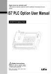
1
Right choice for ultimate yield
LSIS strives to maximize customers' profit in gratitude of choosing us for your
partner.
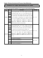
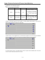
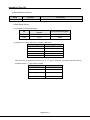
iS7 PLC Option User Manual
SV-iS7 PLC Option Card
z Read
this manual carefully before
installing, wiring, operating, servicing
or inspecting this equipment.
z Keep
this manual within easy reach
for quick reference.
Chapter 1 General
1.1 Guide to Use This Manual··············································································1 - 1
1.2 Features ·······································································································1 - 2
1.3 Terminology ··································································································1 - 3
Chapter 2 system Configuration
2.1 Overall System Configuration ······································································2 - 1
2.1.1 Basic System ·······················································································2 - 1
2.1.2 Product Block Diagram ········································································2 - 2
2.2 Exterior of Product ························································································ 2 – 3
Chapter 3 General Specification
3.1 General Specification ···················································································3 - 1
Chapter 4 CPU Function
4.1 CPU Performance Specification ···································································4 - 1
4.2 Operation Processing ···················································································4 - 2
4.2.1 Operation Processing Method ·····························································4 - 2
4.2.2 Operation Processing at Momentary Power Failure Occurrence ··········4 - 3
4.2.3 Scan Time ····························································································4 - 3
4.2.4 Scan Watchdog Timer ··········································································4 - 4
4.2.5 Timer Processing ·················································································4 - 4
4.2.6 Counter Processing ··············································································4 - 7
4.3 Program ········································································································4 - 9
4.3.1 Classification of Program ·····································································4 - 9
4.3.2 Program Execution Procedure ···························································4 - 10
4.3.3 Interrupt Program ··········································································
4 - 11
4.3.4 Error Handling ··················································································· 4 – 13
4.4 Operation Mode ··························································································4 - 14
4.4.1 RUN mode ·························································································4 - 14
4.4.2 STOP mode ························································································4 - 15
4.4.3 PAUSE mode ·····················································································4 - 15
4.4.4 Operation mode change method ·······················································4 - 15
4.5 Function ······································································································4 - 17
4.5.1 Self-diagnosis ·····················································································4 - 17
4.5.2 Forced Input/Output On/Off function…………………………………… ·4 - 17
4.5.3 Direct I/O operation function ······························································4 - 20
4.5.4 System Error History ··········································································4 - 20
4.6 Memory Configuration ················································································4 - 22
4.7 RTC Function ·····························································································4 - 23
4.7.1 Usage···································································································4 - 23
Chapter 5
Input and Output Function
5.1 Input and Output Specification ·····································································5 - 1
5.2 Digital Input Specification ············································································ 5 – 2
5.3 Digital Output Specification ········································································· 5 – 4
Chapter 6 Usage of Various Function
6.1 Built-in Functions ························································································· 6 – 1
6.1.1 Pulse Catch Function ···········································································6 - 1
6.1.2 Input Filter Function ·············································································6 - 3
6.1.3 External Interrupt Function·····································································6 - 4
6.1.4 PID Control Function············································································· 6 – 6
Chapter 7 Exclusive Functions for iS7 Inverter Control/Monitoring
7.1 Outline and Installation···················································································7 - 1
7.1.1 Outline and Major Components of the Product ····································7 - 1
7.1.2 Detail description of the components ···················································7 - 3
7.2 Functions of PLC option card exclusively for iS7 inverter ····························7 - 9
7.2.1 List of the special D registers for iS7 inverter control and monitoring ···7 - 9
7.2.2 Control (PLC Option Æ Inverter)·························································7 - 10
7.2.3 Monitoring (PLC Option Inverter) ····················································7 - 14
Chapter 8 Modbus Communication
8.1 Modbus Communication··············································································· 8 – 1
8.1.1 Introduction ····························································································8 - 1
8.1.2 Basic Specification ···············································································8 - 1
8.1.3 Parameter Setting ················································································8 - 4
8.1.4 Instruction
·························································································· 8 – 6
Chapter 9 Maintenance
9.1 Maintenance and Inspection ········································································9 - 1
9.2 Daily Inspection······························································································9 - 1
Chapter 10 Troubleshooting
10.1 Basic Procedures of Troubleshooting ························································10 - 1
10.2 Troubleshooting··························································································10 - 1
10.2.1 Troubleshooting flowchart used when the ERR LED is flickering······10 - 2
10.2.2 Troubleshooting flowchart used when the RUN LED turns off. ·········10 - 3
10.2.3 Troubleshooting flowchart used when the I/O part doesn’t operate normally
······················································································································10 - 4
10.2.4 Troubleshooting flowchart used when a program cannot be written to the CPU
part ················································································································10 - 6
10.3 Troubleshooting Questionnaire ··································································10 - 7
10.4 Troubleshooting and Countermeasure ·····················································10 - 8
10.4.1 Input circuit troubles and corrective actions·······································10 - 8
10.4.2 Output circuit troubles and corrective actions ··································10 - 9
10.5 Error Code List ······················································································· 10 - 11
Appendix
Appendix 1. System Definitions ·························································Appendix 1 - 1
Appendix 2. Flag List··········································································· Appendix 2 – 1
Appendix 3. Control and Monitoring Specific Inverter Data ·················Appendix 3 - 1
Appendix 4. Common Area Parameter of iS7 Inverter·························Appendix 4 - 1
Safety Instructions
SAFETY INSTRUCTIONS
Before using the product …
For your safety and effective operation, please read the safety instructions thoroughly before using the product.
► Safety Instructions should always be observed in order to prevent accidents or risks with the safe and
proper use of the product.
► Instructions are separated into “Warning” and “Caution”, and the meaning of the terms is as follows;
Warning
This symbol indicates the possibility of serious injury or death if some applicable
instruction is violated
Caution
This symbol indicates the possibility of slight injury or damage to products if some
applicable instruction is violated
► The marks displayed on the product and in the user’s manual have the
following meanings.
Be careful! Danger may be expected.
Be careful! Electric shock may occur.
► The user’s manual should be kept available and accessible to any user of the product even after it’s been
read.
1
Safety Instructions
Design Precautions
Warning
Install a safety circuit external to the PLC that keeps the entire system safe even when
there are problems with the external power supply or the PLC module. Otherwise,
serious trouble could result from erroneous output or erroneous operation.
- Outside the PLC, construct mechanical damage preventing interlock circuits such as
emergency stop, protective circuits, positioning upper and lower limits switches and
interlocking forward/reverse operation.
When the PLC detects the following problems, it will stop calculation and turn off all output in
the case of watchdog timer error, module interface error, or other hardware errors.
However, one or more outputs could be turned on when there are problems that the PLC
CPU cannot detect, such as malfunction of output device (relay, transistor, etc.) itself or I/O
controller. Build a fail safe circuit exterior to the PLC that will make sure the equipment
operates safely at such times. Also, build an external monitoring circuit that will monitor any
single outputs that could cause serious trouble.
Make sure all external load connected to output does NOT exceed the rating of output
module.
Overcurrent exceeding the rating of output module could cause fire, damage or erroneous
operation.
Build a circuit that turns on the external power supply when the PLC main module
power is turned on.
If the external power supply is turned on first, it could result in erroneous output or erroneous
operation.
2
Safety Instructions
Safety Instructions for design process
Caution
Do not bunch the control wires or communication cables with the main circuit or power wires, or
install them close to each other. They should be installed 100mm (3.94inch) or more from each
other.
Installation Precautions
Caution
Use the PLC option card in an environment that meets the general specification contained in
this manual or datasheet.
Using the PLC option card in an environment outside the range of the general specifications could
result in electric shock, fire, erroneous operation, and damage to or deterioration of the product.
Completely turn off the power supply before loading or unloading the module.
Not doing so could result in electric shock or damage to the product.
Make sure all modules are loaded correctly and securely.
Not doing so could cause a malfunction, failure or drop.
Make sure I/O and extension connector are installed correctly.
Poor connection could cause an input or output failure.
When install the PLC option card in environment of much vibration, be sure to insulate the
PLC option card from direct vibration.
Not doing so could cause electric shock, fire, and erroneous operation.
Be sure to there are no foreign substances such as conductive debris inside the module.
Conductive debris could cause fires, damage, or erroneous operation.
3
Safety Instructions
Wiring Precautions
Warning
Completely turn off the external power supply when installing or placing wiring.
Not doing so could cause electric shock or damage to the product.
Make sure that all terminal covers are correctly attached.
Not attaching the terminal cover could result in electric shock.
Caution
Be sure that wiring is done correctly be checking the product’s rated voltage and the terminal
layout.
Incorrect wiring could result in fire, damage, or erroneous operation.
Tighten the terminal screws with the specified torque.
If the terminal screws are loose, it could result in short circuits, fire, or erroneous operation.
Be sure to ground the FG or LG terminal to the protective ground conductor.
Not doing so could result in erroneous operation.
Be sure there are no foreign substances such as sawdust or wiring debris inside the module.
Such debris could cause fire, damage, or erroneous operation.
4
Safety Instructions
Startup and Maintenance Precautions
Warning
Do not touch the terminals while power is on.
Doing so could cause electric shock or erroneous operation.
Switch all phases of the external power supply off when cleaning the module or retightening
the terminal or module mounting screws.
Not doing so could result in electric shock or erroneous operation.
Do not charge, disassemble, heat, place in fire, short circuit, or solder the battery.
Mishandling of battery can cause overheating or cracks which could result in injury and fires.
Caution
Do not disassemble or modify the modules.
Doing so could cause trouble, erroneous operation, injury, or fire.
Switch all phases of the external power supply off before mounting or removing the module.
Not doing so could cause failure or malfunction of the module.
Use a cellular phone or walky-talky more than 30cm (11.81 inch) away from the PLC option
card.
Not doing so can cause a malfunction.
Disposal Precaution
Caution
When disposing of this product, treat it as industrial waste.
Not doing so could cause poisonous pollution or explosion.
5
Chapter 1 General
Chapter 1 General
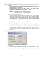
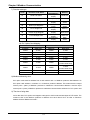
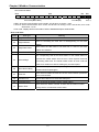
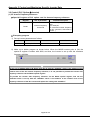
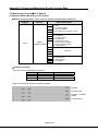
1.1 Guide to Use This Manual
This manual includes specifications, functions and handling instructions for the PLC
option card for dedicated iS7 inverter. This manual is divided up chapters as follows:
No.
Title
Chapter 1
General
Chapter 2
Chapter 3
System
Contents
Describes configuration of this manual, unit’s for features
and terminology.
Describes available units and system configuration in the
Configuration
General
iS7 PLC option card.
Describes general specifications of units used in the PLC
Specification
option card.
Chapter 4
CPU
Chapter 5
Input and Output
Describes each kind of Manufactured goods’ usage and
Usage of Various
specifications.
Chapter 6
Functions
iS7 Inverter
Chapter 7
Control/Monitoring
Describes
Communication
Maintenance
Chapter 10
Troubleshooting
Appendix 1
System Definitions
Appendix 2
Flag List
Control and
Appendix 3
Monitoring Specific
Appendix 4
function
which
is
card.
Describes the items to be checked for long-term normal
operation of the iS7 PLC option card.
Describes the various operation errors and corrective
actions.
Describes
parameter
setting
for
basic
I/O
and
communications module.
Describes the types and contents of various flags.
Describes enables control or monitoring of the specific
data of inverter.
Inverter Data
Common Area
important
Describes the built-in communication function of PLC option
Function
Chapter 9
most
control/monitoring of PLC option card of iS7 inverter.
Function
Chapter 8
the
Describes the common area parameter of iS7 inverter need
Parameter of iS7
ed for control/monitoring of iS7 inverter.
Inverter
Remark
-. This manual does not describe the programming method. For their own functions, refer
to the related user's manuals.
1-1
Chapter 1 General
1.2 Features
1) iS7 PLC option card is compact type which is integrated the function of CPU, Input and output,
and communication function. PLC option card has features of below described.
(1) High speed processing
High speed processing of 0.1μs/Step
(2) Various built-in functions
PLC option card can perform the various system by just using the one option card.
• Fast processing applications
- Pulse catch: Allows the option card to read a pulse which has a width as small as 10 ㎲.
- External interrupt: Using in various applications with built-in 6 interrupt input that
high-priority event which requires immediate responses.
• The input filter function helps to reduce the possibility of false input conditions from
external noise, such as signal chattering. The filter time can be programmed from 0 to
1000ms.
• Using RS-232C and RS-485 built-in port, the option card can connect with external
devices, such as personal computers or monitoring devices and communicate 1:N
with external device.
• Using built-in PID control function, PID control system can be constructed without
using separate PID module.
(3) Battery-less
The user’s program can be saved permanently without battery, because it is stored in
EEPROM.
(4) When program is edited during processing, it is stored in EEPROM automatically.
(5) It supports the Master function at Modbus-RTU protocol.
(6) It can easily do On/Off of the system, using RUN/STOP switch.
(7) it can save the program permanently in EEPROM by easy editing with KGLWIN.
(8) Strong self-diagnostic function
It can detect the cause of errors with more detailed error codes.
(9) It can prevent unintentional reading and writing, using password.
(10) Various program execution functions
External and internal interrupt program as well as scan program can be executed by
setting the execution condition. Therefore, user can set various program execution
modes.
1-2
Chapter 1 General
1.3 Terminology
The following table gives definition of terms used in this manual.
Terms
Definition
Remarks
A programming and debugging tool for the MASTER-K
KGLWIN
series. It executes program creation, edit, compile and
-
debugging (A computer software).
I/O Image Area
Internal memory area of the CPU module which is used
to hold I/O statuses.
-
Abbreviation of ‘Real Time Clock’. It is used to call
RTC
-
general IC that
contains clock function.
Supervises the pre-set execution times of programs and
Watchdog Timer
warns if a program is not completed within the pre-set
time.
1-3
-
Chapter 2 System Configuration
Chapter 2 System Configuration
2.1 System Configuration
2.1.1 Basic System
Input points
6 Points (NPN/PNP))
Output points
Relay output 4 points
RS232C
RS485
Display LED
Switch
1 port (Program download from KGLWIN)
1 port (Modbus-RTU Master/Slave)
2 ea (Green: RUN LED, Red: ERROR LED)
3 step switch for RUN, PAU/REM, STOP
Clock function
Built-in RTC (Real Time Clock)
Data Back-up
Data of latch area and RTC data through using CR2032 lithium
battery)
2-1
Chapter 2 System Configuration
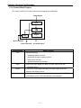
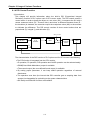
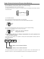
2.1.2 Product Block Diagram
PLC option card for iS7 inverter series’ block diagram is as following.
Input Signal
Input
CPU
Comm
Output
Built-in RS-485
Built-in RS-232C I/F Output Signal
Classification
CPU
Main Function
• Signal processing
-. Operating System function
-. Application program saving function
-. Data saving function
-. Application execution function
Input
• Convert the input signal and data to proper signal level from
controlled device.
Output
• Convert the output signal and data to proper signal level from
actuator and display device.
Communication
•
Configure the 1:1 communication system to connect with PADT
(KGLWIN) or built-in RS-232C/RS485 communication.
2-2
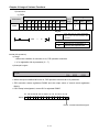
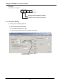
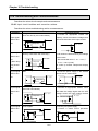
Chapter 2 System Configuration
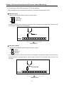
2.2 Exterior of Product
Symbol
Name
Usage
LED1
RUN LED
On state: Local Run (SW1 position is RUN) or Remote Run (SW1
position is PAU/REM) and Select the RUN icon at KGLWIN.
LED2
ERR LED
1) Flickering : It flickering when Error is occurred.
2) OFF : It is Off at normal operation.
SW1
Mode Switch
1) RUN position : Program Execution
2) PAU/REM position : Temporary stop, Remote Rung/Stop
Execution etc.
3) STOP position : Program Stop
1) Factory default state. Do not use other setting. Please
contact LSIS customer service center.
Normal
State
J1
PLC OS Download
Jumper
2) Do not operate the jumper as below setting. Please
contact LSIS customer service center.
OS Download mode
J2
Terminal Selection
Jumper
1) ON: Select the communication terminal resistor of RS485.
(Built-in resistor 120 ohm.)
2) OFF: None
2-3
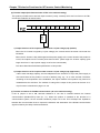
Chapter 2 System Configuration
Symbol
Name
Usage
1) NPN mode: Connect terminal input (P00~P05) with 24G.
NPN mode
J3
NPN/PNP
Selection jumper
2) PNP mode: Connect the terminal input (P00~P05) with
24P.
PNP mode
CON1
Battery
TB1
RS232C
communication
connector
Battery Insertion
part
Terminal Blcok
Connector to communicate with KGLWIN
1) Function : Maintaining of the Latch area data and RTC
data at power failure
2) Battery type: Coin type lithium battery (CR2032)
3) Life : about 4 years with power off (normal temperature,
capacity 220mAh assumed)
1: S+(RS485)
3: 24G
5: Terminal InputP01
7: Terminal InputP03
9: Terminal InputP05
11: 24P (output 24V)
12: Terminal Output P40
14: Terminal Output P41
16: Terminal Output P42
18: Terminal Output P43
2-4
2: S-(RS485)
4: Terminal InputP00
6: Terminal InputP02
8: Terminal InputP04
10: 24G
13: Terminal Output P40C
15: Terminal Output P41C
17: Terminal Output P42C
19: Terminal Output P43C
Chapter 3 General Specifications
Chapter 3 General Specifications
3.1 General Specifications
The following table shows the general specifications of the PLC option card for iS7 inverter series.
No.
Item
Specifications
References
Operating ambient
1
Temperature
Storage ambient
2
Temperature
Operating ambient
3
Humidity
Storage ambient
4
Humidity
Vibrations
5
Shocks
6
Noise Immunity
7
0 ~ 55 °C
-
−25 ~ +70 °C
-
5 ~ 95%RH, non-condensing
-
5 ~ 95%RH, non-condensing
-
Occasional vibration
Frequency
Acceleration
10 ≤ f < 57Hz
−
9.8m/s2 {1G}
57 ≤ f ≤ 150Hz
Continuous vibration
Frequency
Acceleration
10 ≤ f < 57Hz
−
2
57 ≤ f ≤ 150Hz 4.9m/s {0.5G}
Atmosphere
9
Altitude
10
11
Amplitude
0.035mm
−
10 times for
each
X, Y, Z axis
-
IEC 61131-2
• Maximum shock acceleration: 147 m/s2 {15G}
• Duration time: 11ms
• Pulse wave: half sine pulse (3 shocks per axis, on X, Y, Z axis)
IEC 61131-2
Square wave
Impulse noise
± 1,500 V
LSIS’ Internal
Standard
Voltage: 4 kV ( Discharge by contact )
IEC 61131-2,
IEC 1000-4-2
27 ~ 500 MHz, 10 V/m
IEC 61131-2,
IEC 1000-4-3
Power
supply
Voltage
2kV
IEC 61131-2
IEC 1000-4-4
Electronic
discharge
Radiated
electromagnetic
field noise
Fast transient &
Burst noise
8
Amplitude
0.075mm
−
Sweep count
Item
Digital I/O/Analog I/O
Communication Interface
1kV
Free of corrosive gases and excessive dust
-
Up to 2,000m
-
Pollution degree
Less than 2
-
Cooling method
Air-cooling
-
REMARK
1) IEC (International Electrotechnical Commission): An international civilian institute who establishes
international standards in the area of electric and electronics.
2) Pollution degree: An indicator, which indicates pollution degree, which determine insulation
performance of equipment.
* Pollution degree 2: Normally, only non-conductive pollution occurs. Occasionally, however, a
temporary conductivity caused by condensation shall be expected.
3-1
Chapter 4 CPU Function
Chapter 4 CPU Function
4.1 CPU Performance Specification
The following table shows the general specifications of the PLC option card of iS7 inverter.
Item
Specifications
Program Control Method
Remark
Cyclic execution of stored program, Time-driven interrupt, Processdriven interrupt
-
I/O Control Method
Indirect mode(Refresh method), Direct by program command
-
Program Language
Ladder Diagram Program, Instruction List Program
-
29
-
223 Instructions (note 1)
-
Program Capacity
2 ksteps
-
I/O Points
Digital Input 6 points/Digital Output (Relay) 4 points
-
Number
Instruction
of Basic
Application
P
P000 ~ P0005 (External Input), P0040 ~ P0043 (External Output)
M
M000 ~ M191F
K
K000 ~ K31F
Keep Relay
L
L000 ~ L63F
Link Relay
F
F000 ~ F63F
Special Relay
Memory
I/O Relay
Internal Relay
- 100ms: T000 ~ T191 (192 points)
Device
T
- 10ms: T192 ~ T250 (59 points)
Timer
- 1ms: T251 ~ T255 (5 points), Adjustable by parameter setting
C
C000 ~ C255
S
S00.00 ~ S99.99
Step Relay
D
D0000 ~ D4999
Data Register
Counter
Operation Methods
RUN, STOP, PAUSE
-
Self-diagnosis Functions
Detects errors of scan time, memory, I/O and power supply
-
Data Back-up Method at
Data of Latch and RTC area at basic parameter is reserved when
Power Interruption
power is turned Off/On with mercury battery (CR2032).
PID Control
Function
Cnet I/F
Built-in
Function
-
Controlled by commands, Relay and PRC auto tuning,
PWM output, manual output, adjustable operation scan time,
-
Anti-windup, SV-Ramp, Delta MV, Position and Velocity algorithm
MODBUS protocol supported (RS-485 1 port)
-
6 points
-
Input Filter
0 ~ 1000 ms (Adjustable via Basic Parameter)
-
RTC Function
Year/Month/Day/Time/Minute/Second (Available to set by KGLWIN)
-
Function
External
Interrupt
(note 1)
Except for DRCV, DSND, HMDA, HMDAP, HMDB, HMDBP, HSC, HSCST, PLSOUT, POSCTR, POSDST, POSIST,
POSJOG, POSORG, POSPRS, POSSOR, POSVEL, PWM, SCAL, SCALP, SND8, SNDCOM Instructions
4-1
Chapter 4 CPU Function
4.2 Operation Processing
4.2.1 Operation Processing Method
1) Cycle operation
A PLC program is sequentially executed from the first step to the last step, which is called scan. This sequential
processing is called cyclic operation. Cyclic operation of the PLC option card continues as long as conditions
do not change for interrupt processing during program execution. This processing is classified into the following
stages:
Stages
Processing
Operation Start
-
Stage for the start of a scan processing. It is executed only one
Initialization
time when the power is applied or reset is executed. It executes
the following processing.
▶ I/O reset
▶ Execution of self-diagnosis
▶ Data clear ▶ Allocating I/O address and type
Input Image Area Refresh
Input conditions are read and stored into the input image area
before it starts processing.
Program operation processing
Program starts
Program is sequentially executed from the first step to
the last step Program operation processing.
Program ends
Output image area refresh
The contents stored in the output image area is output to output
part when operation processing of a program is finished.
END processing
Stage for return processing after the CPU part has finish
ed 1 scan.
The END processing following processing is executed.
▶ Self-diagnosis
▶ Change present values of timer and counter, etc.
▶ Processing data communications between computer
link module and communications module.
▶ Checking the switch for mode setting.
2) Interrupt operation method
If a situation occurs which is requested to be urgently processed during execution of a PLC progra
m, this operation method processes immediately the operation, which corresponds to interrupt progr
am. The signal, which informs the CPU of those urgent conditions is called interrupt signal. The C
PU has two kinds of interrupt operation methods, which are internal and external interrupt signal me
thods.
4-2
Chapter 4 CPU Function
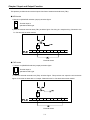
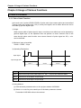
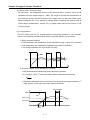
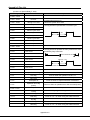
4.2.2 Operation Processing at Momentary Power Failure Occurrence
The momentary power failure occurs when the input line voltage to the power supply falls down
below the rated voltage. When momentary power failure occurs within 10ms, the PLC option card
maintain operation processing. But if it exceeds 10ms, PLC option card stops processing and all
output turns off. And The re-start process is executed as the power is re-applied.
1) Momentary power failure within 10 ms
→ The operation processing is maintained.
Input
Power
Momentary power failure
within 1Oms
2) Momentary power failure exceeding 10 ms
→ The re-start process is executed as the power is
re-applied.
Input
Power
Power failure exceeding
Remark
1) Momentary power failure
The PLC option card defining power failure is a state that the voltage of power has been
lowered outside the allowable variation range of it. The momentary power failure is a power
failure of short interval (several to tens ms).
4.2.3 Scan Time
The processing time from a 0 step to the 0 step of next scan is called scan time.
1) Expression for scan time
Scan time is the sum of the processing time of scan program that the user has written, of the
task program processing time and the PLC option card internal processing time.
(1) Scan time = Scan program processing time + Interrupt program processing time +
PLC option card internal processing time
• Scan program processing time = The processing time used to process a user program
that is not specified to a task program.
• Interrupt program processing time = Total of the processing time of interrupt programs
executed during one scan.
• PLC option card internal processing time = Self-diagnosis time + I/O refresh time + Inte
rnal data processing time + Communications service proce
ssing time
4-3
Chapter 4 CPU Function
(2) Scan time differs in accordance with the execution or non-execution of interrupt progr
ams and communication processing, etc.
2) Scan time monitoring
Scan time is stored in the following system flag area.
• F50 : Maximum scan time (unit: 1 ms)
• F51 : Minimum scan time (unit: 1 ms)
• F52 : Current scan time (unit: 1 ms)
4.2.4 Scan Watchdog Timer
1) Watchdog timer is used to detect a delay which is attributable to abnormal operation of
sequence program. (Watchdog time is set in menu of basic parameter of KGLWIN.)
2) When watchdog timer detects an exceeding of preset watchdog time, the operation of P
LC option card is stopped immediately and all output is off.
3) If an exceeding of preset watchdog time is expected in sequence program, use ‘WDT’
instruction. ‘WDT’ instruction makes elapsed watchdog time to zero.
4) In order to clear watchdog error, restart the PLC option card or change mode to STOP.
Remark
- Setting range of watchdog : 10 ~ 6,000ms (unit : 10ms)
4.2.5 Timer Processing
The PLC option card use up count timer. There are 5 timer instructions such as On-delay
Timer (TON), Off-delay Timer (TOFF), Integral (TMR), Monostable (TMON), Retreggerable
(TRTG). The measuring range of 100msec timer is 0.1 ~ 6553.5 seconds, 10msec timer is
0.01 ~ 655.35 seconds.
Txxx
Txxx
xxxxx
Timer Preset Value
Timer Contact Number
Timer Type
4-4
Chapter 4 CPU Function
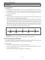
1) Current value update and Contact On/Off of On Delay Timer
The current value of timer is updated when the input condition of TON instruction turns On. When the
current value reaches the preset value (current value = preset value), the timer output relay (Txxx)
turns On.
Timer Output Relay
Timer Preset Value
(PT)
t0
t1
t2 t3
t1
t0+PT
Timer Current Value
(ET)
t0
t5
t4
t4+PT
t1
t2 t3
t4
t5
t5
2) Current value update and Contact On/Off of Off Delay Timer
The timer output relay (Txxx) is turned On when the input condition of TOFF is turned On. When the
input condition is turned off, the current value starts to decrease. The timer output relay (Txxx) is
turned Off when the elapsed time reaches to preset time (current value = preset value). Timer
diagram of Off Delay Timer is as below.
Timer Input
Condition
t1
t0
Timer Output Relay
t0
Timer Preset Value (PT)
t2
t1+PT
t3
t4
t5
t2
t5+PT
Timer Current Value (ET)
t1
t5
t3
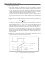
3) Current value update and Contact On/Off of Integral Timer
The current value will be increased when input condition is turned On. Timer output relay is turned
On when the current value reaches to timer preset value. Timer output relay turned On keeps the
status before reset input is turned On. Timer diagram of Integral timer is as below.
Timer Input
Condition
t0
t1
t4
t2
Timer Output Relay
t4+PT
PT=t1-t0+t3-t2
Timer Preset Value (PT)
Timer Current Value (ET)
t0
t1
t2
t4
t3
Timer Reset Input
4-5
Chapter 4 CPU Function
4) Current value update and Contact On/Off of Monostable Timer
In general, its operation is same as off-delay timer. However, the change of input condition is ignored
while the timer is operating (decreasing). When current value reaches preset value the timer output
relay is turned off and current value is cleared. Timer diagram of Monostablel timer is as below.
Timer Input
Condition
t0
t1
t2
t3
t4
t2
t2+PT
t4
Timer Output Relay
Timer Preset Value
(PT)
t0
Timer Current Value
(ET)
t0
t0+PT
t1
t4+PT
t4
t2
5) Current value update and Contact On/Off of Retriggerable Timer
The operation of retriggerable timer is same as that of monostable timer. Only difference is that the
retriggerable timer is not ignore the input condition of TRTG instruction while the timer is operating
(decreasing). The current value of retriggerable timer will be set as preset value whenever the input
condition of TRTG instruction is turned on.
Timer Input
Condition
t2
t0
t3
Timer Output Relay
t2
Timer Preset Value
(PT)
Timer Current Value
(ET)
t0
t2=PT
t3
t1
t3=PT
t4
Remark
Timing Error
- The Maximum timing error of timers of PLC option card is ‘1 scan time + the time from 0 step to timer instruction’
4-6
Chapter 4 CPU Function
4.2.6 Counter Processing
The counter counts the rising edges of pulses driving its input signal and counts once only
when the input signal is switched from off to on. PLC option card have 4 counter instructions
such as Up Counter (CTU), Down Counter(CTD), Up/Down Counter (CTUD), and Ring
Counter (CTR). The followings shows brief information for counter operation.
• Up Counter (CTU) increases the current value.
• Down Counter (CTD) decreases the current value.
• Up/Down Counter (CTUD) compares the 2 input conditions’ value.
• Ring Counter (CTR) clear the current value as 0 when current value reaches to set value by
increasing the current value.
1) Current value update and Contact On/Off
(1) Up Counter
• Input Condition (U), Reset Condition (R), and preset value must be existed.
-. The counter output relay is turned on when the current value reaches the preset value.
-. When the reset input is turned on, the counter output relay and current value is cleared as 0.
(2) Down Counter
• Input Condition (U), Reset Condition (R), and preset value must be existed.
-. When reset signal is turned on, current value reaches to preset value and output relay is
turned off.
-. The counter output relay is turned on when the current value reaches 0.
(3) Up/Down Counter
• 2 kinds of Input Condition, Reset Condition and Preset Value must be existed.
-. When Reset signal is inputted, current value is turned to 0.
-. The current value is increased with the rising edge of up-count input signal, and
decreased with the rising edge of down-count input signal.
-. The counter output relay is turned on when the current value is equal or greater than the
preset value otherwise off.
4-7
Chapter 4 CPU Function
(4) Ring Counter
• Input Condition (D), Reset Condition (R), and preset value must be existed.
-. The current value is increased with the rising edge of the counter input signal, and the
counter output relay is turned on when the current value reaches the preset value. Then
the current value and counter output relay is cleared as 0 when the next counter input
signal is applied.
2) Maximum Counting Speed of Counter
The maximum counting speed of counter is determined by the length of scan time. Counting
is possible only when the on/off switching time of the counter input signal is longer than scan
time.
Max. Counting Speed
C max =
1
n
× (− )
100
tS
n : Duty (%)
t S : Scan Time [s]
Duty is the ratio of the input signal’s on time to off time as a percentage.
On
Off
Off
T1
T1 ≤ T2, n =
T1 > T2, n = -
T2
T1
T1+T2
T2
T1+T2
4-8
X 100 [%]
X 100 [%]
Chapter 4 CPU Function
4.3 Program
4.3.1 Classifications of Program
All functional elements need to execute a certain control process are called as a ‘program’. In PLC
option card, a program is stored in the EEPROM mounted on a CPU module or flash memory of a
external memory module. The following table shows the classification of the program.
Program type
Scan program
Description
The scan program is executed regularly in every scan
The TDI programs are executed with a constant time interval specified
Time-driven
with parameter setting as below case.
interrupt program
▶ If process time is needed faster than average 1 scan time,
(TDI)
▶ If process time is needed longer than average 1 scan time,
▶ If process time is needed with constant time interval,
Process driven
interrupt program
(PDI)
High speed counter
driven interrupt
program (HSCDI)
• The PDI programs are executed when external interrupt input is
applied.
• This interrupt programs are executed when comparison task signal is
applied.
Subroutine
• The subroutine programs are executed when they are called by the
program
scan program with a CALL instruction.
4-9
Chapter 4 CPU Function
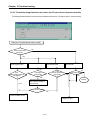
4.3.2 Program Execution Procedure
The following diagram shows that how the CPU module process programs when the CPU
module is powered on or switched to
RUN mode.
Start Processing
Subroutine Program
PDI Program
Scan Program
TDI Program
It is executed when
the condition is
satisfied.
End Processing
1) Scan Program
(1) Function
-. The scan program is executed regularly in every scan from 0 step to last step.
-. When interrupts has occurred, CPU pauses scan program and executes corresponding
interrupt program first.
-. When this interrupt program finished, scan program is to resume.
2) Interrupt Program
(1) Function
-. When an interrupt occurs, the CPU module will stop the current operation and execute the
corresponding interrupt routine first. After finish the interrupt routine, the CPU resume the
sequence program from the stopped step.
(2) Type
• PLC Option card provides 2 types of interrupt.
- The TDI (Time driven interrupt) occurs with the constant period
- The PDI (Process driven interrupt) occurs with the status of external input.
4 - 10
Chapter 4 CPU Function
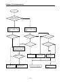
4.3.3 Interrupt Program
It describes the program structure of KGLWIN and Interrupt program to help your understanding
of Interrupt function of PLC option card . (Please refer to KGLWIN user manual for KGLWIN
programming.)
Scan Program
Interrupt 1
Interrupt routine 1
(Program 1)
Interrupt 2
Interrupt routine 2
(Program 2)
Interrupt routine 3
Interrupt 3
Interrupt 2
(Program 3)
(Program 2)
Interrupt routine 2
Interrupt 4
(Program 4)
Interrupt routine 4
Remark
-. Interrupt routine should be written after END instruction.
END
-. An interrupt factor that has higher priority occurs while
other interrupt that has lower priority are executing, the
interrupt routine of lower priority will be stopped and the
interrupt of higher priority will be executed first.
-. All interrupts’ status is Disable when power is applied.
-. To execute an interrupt routine, use the EI instruction to
enable the corresponding interrupt.
4 - 11
Chapter 4 CPU Function
1) Parameter Setting
2) Time-driven Interrupt
Time-driven interrupt occurs periodically with the constant interval assigned in parameter setting. In PLC
option card of iS7 inverter series, Available TDI is P000 ~ P007 (8 points) assigned in parameter setting
and period can be designated for each other.
3) Process-driven Interrupt
Available Process-driven interrupt is P000 ~ P005 (6 points) assigned in parameter setting.
In the parameter setting window, TDINT indicates time driven interrupt and INT indicates process
driven interrupt. (Edge setting can select Up, Down, Up/Down of input signal when Process-driven
interrupt is selected.)
Remark
-. Interrupt signal is ignored when self-interrupt occurs more than 2 times during interrupt processing is
executing.
Interrupt executing
Interrupt signal
(ex : rising edge)
It is ignored.
It process the only final signal.
-. Interrupt program is available to maximum 8 points. If Process-driven interrupt used one, Time-driven interrupt
can use maximum 7 points.
4 - 12
Chapter 4 CPU Function
4.3.4 Error Handling
1) Classification of Errors
Errors occur due to various causes such as PLC option card system defect, system configuration
fault or abnormal operation result. Errors are classified into fatal error mode, which stops system
operation for system stability, and ordinary error mode, which continues system operation with inf
orming the user of its error warning.
The main factors that occurs the PLC option card error are given as followings.
• PLC option card hardware defect
• System configuration error
• Operation error during execution of the user programs
• External device malfunction
2) Operation mode at error occurrence
In case of error occurrence, the PLC option card write the error contents the correspond
ing flags and stops or continues its operation complying with its operation mode.
(1) PLC option card hardware defect
The system enters into the STOP state if a fatal error such as the CPU module def
ect has occurred, and continues its operation if an ordinary error such as operation
error has occurred.
(2) System configuration error
This error occurs when the PLC option card hardware configuration differs from the c
onfiguration defined in the PLC option card. The system enters into the STOP state.
(3) Operation error during execution of the user programs
It the numeric operation error of these errors occurs during execution of the user pr
ogram, its contents are marked on the error flags and the system continues its oper
ation. If operation time overruns the watchdog time or I/O modules loaded are not n
ormally controlled, the system enters into the STOP state.
(4) External device malfunction
The PLC option card user program detects malfunctions of external devices. If a fatal
error is detected the system enters into the STOP state, and if an ordinary error is
detected the system continues its operation.
Remark
1) In occurrence of a error, the state is to be stored in the representative system error
flag F006.
2) For details of flags, refer to Troubleshooting.
4 - 13
Chapter 4 CPU Function
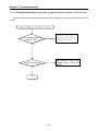
4.4 Operation Mode
The CPU operates in one of the three modes - RUN, STOP, and PAUSE mode. The followi
ng describes operation processing in each operation mode.
4.4.1 RUN mode
In this mode, programs are normally operated.
The first scan start in the RUN
Initialize data area according to the
preset restart mode.
Check the program and determine it
can be executed or not.
Execute input refresh
Execute programs and Interrupt
tasks
Check the availability of expansion
units
Execute communication and internal
i
Execute output refresh
No
Operation mode is changed?
Yes
Operate with new mode.
4 - 14
Chapter 4 CPU Function
1) Processing when the operation mode is changed.
Initialization of data area is executed when the first scan starts and The possibility of exec
ution of the program is decided with check on its effectiveness.
2) Operation processing contents
I/O Refresh and program operation are executed.
(1) Interrupt programs are executed with the detection of their start-up conditions.
(2) Normal or abnormal operation and mounting conditions of the loaded module are checked.
(3) Communications service or other internal operations are processed.
4.4.2 STOP mode
In this mode, program are not operated. It can transfer the program via KGLWIN in Remote STOP mode.
In this mode, programs are not operated.
1) Processing when the operation mode is changed.
The output image area is cleared and output refresh is executed.
2) Operation processing contents
(1) I/O refresh is executed.
(2) Normal or abnormal operation and mounting conditions of the loaded module are checked.
(3) Communications service or other internal operations are processed.
4.4.3 PAUSE mode
In this mode, the program operation is temporarily stopped. If it returns to the RUN mode, the o
peration continues from the state before the stop.
1) Processing when the operation mode changes
Data registers and input image areas are not cleared and the operating conditions just before t
he mode change is maintained.
2) Operation processing contents
(1) I/O refresh is executed.
(2) Normal or abnormal operation and mounting conditions of the loaded module are checked.
(3) Communications service or other internal operations are processed.
4.4.4 Operation mode change method
1) Operation mode change method
The following method is used to change the operation mode.
(1) Change by the mode key of the PLC option card for iS7.
(2) Change by the KGLWIN connected with communication port of PLC option card’s CPU.
(3) Change by the ‘STOP’ instruction, during program execution.
4 - 15
Chapter 4 CPU Function
2) Operation mode change by mode key
The method of operation mode change by mode key is as below table.
Mode Setting Key Position
RUN
STOP
Operation Mode
Local RUN
Local STOP
Remote RUN: Select Run icon at KGLWIN
PAU / REM
Remote STOP: Select STOP icon at KGLWIN
Remote PAUSE: Select PAUSE icon at KGLWIN
Remark
If the operation mode changes from RUN mode to local RUN mode by the mode setting
key, the PLC option card operates continuously without stopping.
4 - 16
Chapter 4 CPU Function
4.5 Function
4.5.1 Self-diagnosis
1) Function
(1) The self-diagnosis function permits the CPU module of PLC option card to detect its own errors.
(2) Self-diagnosis is carried out when an error occurs during PLC option card power supply is turne
d on or operating process. If an error is detected, the system stops operation to prevent faulty
PLC option card operation.
2) Watchdog Timer
The watch dog timer is an internal timer of a PLC option card to detect the error of hardware and a
sequence program. it is changeable with parameter setting.
The CPU resets the watch dog timer before step 0 is executed (after the END processing is finished).
When the END instruction has not been executed within the set value due to an error occurred in the
PLC option card or the delay of a sequence program, the watch dog timer will times out. When a
watch dog timer error is occurred, all outputs of the PLC option card are turned OFF, and the ERR
LED of the CPU will flickers. (RUN LED will be turned OFF) Therefore, when use FOR ~ NEXT or
CALL instruction, insert WDT instruction to reset the watch dog timer.
0
WDT
WDT Reset
WDT Reset
END
0
END
WDT
3) Error History
When error occurs in CPU, Corresponding error code is stored in special relay F006.
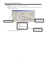
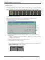
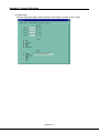
4.5.2 Forced Input/Output On/Off function
It is possible to input/output a designated data regardless of the program operation results. When used
with OUTOFF instruction simultaneously, OUTOFF is prior to Forced I/O On/Off.
1) Forced I/O setting
-. Forced I/O on/off setting is applied to input area and output area.
-. Forced I/O on/off should be set for each input and output, the setting operates from the time t
hat Force I/O setting enable’ is set.
-. This setting can be done when I/O modules are not really loaded.
4 - 17
Chapter 4 CPU Function
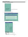
-. Select the ’Set forced I/O’ from KGLWIN
Select ‘Set Forced IO’.
-. Select the I/O area and then double click.
Set ‘forced I/O data’ by bit.
Set ‘forced I/O data enable’ by bit.
4 - 18
Chapter 4 CPU Function
-. When forced I/O set enables, forced I/O function is executing.
Click
2) Special data register for forced I/O
The contents of forced I/O setting is registered to special data register as below.
It is possible to use ‘forced I/O function’ to program.
Items
Special Device
All Forced I/O enable
Forced I/O enable area by bit
Forced I/O set data
M1910
D4700 (Contact Input Enable Area)
D4704 (Contact Output Enable Area)
D4800 (Contact Input Data Area)
D4804 (Contact Output Data Area)
3) Force on/ off Processing timing and method
(1) Forced Input
After data have been read from input modules, at the time of input refresh the data of
the junctions which
have been set to force on/off will be replaced with force setting d
ata to change the input image area. And then, the user program will be executed with
real input data and force setting data.
(2) Force Output
When a user program has finished its execution the output image area has the operatio
n results. At the time of output refresh the data of the junctions which have been set to
force on/off will be replaced with force setting data and the replaced data will be output.
However, the force on/off setting does not change the output image area data while it c
hanges the input image area data.
4 - 19
Chapter 4 CPU Function
(3) Precaution
yTurning the power off and on, changes of the operation mode or operation by reset s
witch does not change the previous force on/off setting data. They remain within the
CPU module and operation is executed with the same data.
y Forced I/O data will not be cleared even in the STOP mode.
y When setting new data, disable every I/O settings using the setting data clear function
and set the new data.
Remark
-. For detailed operation, refer to the KGLWIN user’s Manual Chapter 7 ‘Force I/O setting.
4.5.3 Direct I/O operation function
This function is useful when reads an input relay’s state directly during execution of a program
and uses in the operation, or write the operation result directly to an output relay. Direct
input/output is executed by the ‘IORF’ instruction. If this instruction is used, the input/output
image area will be directly updated and applied to the continuing operations.
4.5.4 System Error History
When the system is stopped by error occurrence, the CPU stores the error occurrence time and
error code to the special data register area.
1) Special data register for Error history
The most recent 16 error occurring times and error codes are stored in the special data
register. If 17th error is occurred, the first error is erased and 17th error history is stored.
Error
Stored
Device
Area
Error Occurred Point
D4901 ~ D4904
The 1st error information
D4905 ~ D4908
The 2nd error information
:
:
D4961 ~ D4964
The 16th error information
2) Description of each word
Data area
Contents
Description
D4900
H0001
Error occurred point
D4901
H0305
Year : 03,
Month : 5
D4902
h2812
Date : 28,
Hour : 12
D4903
h3030
Minute : 30,
D4904
h0001
Second : 30
Error code (h0001)
4 - 20
Chapter 4 CPU Function
3) Clear error data
Use a ‘data clear’ function of KGLWIN.
REMARK
Refer to the KGLWIN user’s Manual Chapter 7, for details.
4 - 21
Chapter 4 CPU Function
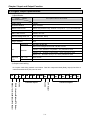
4.6 Memory Configuration
The CPU module includes two types of memory that are available by the user. One is pr
ogram memory, which is used to store the user programs written to implement a system
by the user. The other is data memory, which stores data during operation.
Bit Data Area
0
~
Word Data Area
F
P00
D0000
I/O relay
“P”
P63
M000
M191
K00
(3,040 points)
Special
“M”
T000
T255
T000
Keep relay
K31
F00
F63
L00
L63
(512 points)
“K”
“F”
Link relay
(1,024 points)
T255
C000
C255
C000
“L”
T250
T251
T255
C000
Reserved for special
Timer preset value
(256 words)
(256 words)
Counter preset value
(256 words)
C255
S00
Timer (100ms)
192 points
“D”
Counter elapsed
T000
T191
T192
“T”
value
Step Controller
(100 x 100 steps)
S99
S00.00~S99.99
Timer (10ms)
59 points
“T”
Timer (1ms)
5 points
“T”
Counter
C255
Parameter setting area
Data Register
Timer elapsed value
Special relay
(1,024 points)
FFFF
“M”
auxiliary
relay
~
D4500
D4999
Auxiliary relay
M189
M190
0000
User Program Area
“C”
4 - 22
“S”
Word
User Program Area
Chapter 4 CPU Function
4.7 RTC Function
PLC option card for iS7 inverter series supplies RTC(Real Time Clock) module for the timescheduling control. Clock operation by the RTC function is continued with a super capacitor
when the CPU is powered off. The time of RTC is updated in every scan by operation
information of system flag.
4.7.1 Usage
1) Read/Setting of RTC data
1) Read RTC data
(1) Read RTC data from KGLWIN
-. Select Online –Write Information – Set PLC Clock in menu.
Following message box will be displayed.
4 - 23
Chapter 4 CPU Function
(2) Read RTC data from special register
The followings are the memory address of preset data.
Description
Special register
Area (Word)
Upper byte
Data
(BCD format)
Lower byte
F053
Lower 2 digits of year
Month
H0207
F054
Day
Hour
H2313
F055
Minute
Second
H5020
F056
Higher 2 digits of year
Date
H2002
Example : 2002. 07. 23. 13:50:20, Tuesday
(3) Date expression
Number
0
1
Date
Sunday
Monday
2
3
Tuesday Wednesday
4
5
6
Thursday
Friday
Saturday
2) Time Error
±5 second / 1 month
Remark
1) If RTC stops or error occurs, write new data to the RTC then error is called off.
2) There is no written clock data in the RTC when shipped.
3) Before using RTC module, write clock data to the RTC first.
4) If the range of time is exceeded, RTC is not operated. Ex)14 month 32 day 25 hour
4 - 24
Chapter 5 Input and Output Function
Chapter 5 Input and Output Function
5.1 Input and Output Specification
Digital input that PLC option card of iS7 inverter offers are made to use both electric current sink and
electric current source. (NPN/PNP types) To keep using the coil load as an output module, maximum
opening and shutting frequency is 1 second On and 1 second Off.
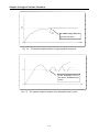
The following diagram shows maximum life relay for relay output.
Frequency (×10,000)
100
50
30
20
10
AC 125 Resistor Load
AC 30 Resistor Load
AC 250 Resistor Load
0.5
1
2
3
5
10
Opening/shutting of electric current (A)
5-1
100
Chapter 5 Input and Output Function
5.2 Digital Input Specification
1) Specification
Specification
Model
PLC Option Card of iS7 Inverter
Number of Input Points
6 Points
Insulation Methods
Photo-coupler Insulation
Rated Input Voltage
DC24V
Rated Input Current
7mA
Operating Voltage Range
DC20.4 ~ 28.8V (Ripple: less than 5%)
Max. simultaneous input points
100% simultaneously On
On Voltage / On Current
DC19V or higher / 5.7 mA or higher
Off Voltage / Off Current
DC6V or lower / 1.8 mA or lower
Input Impedance
About 3.3 kΩ
Response
Off → On
15ms or less (note1)
Time
On → Off
15ms or less (note1)
6 points / COM
Common Terminal
(note1)
It can be set from 0 ms to 1000 ms at KGLWIN.
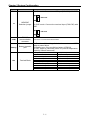
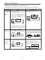
2) Input circuit diagram
PLC option card wiring method is as follows. DC input specifications offered by PLC option card is to
be used for both electric current sink and electric current source. Detailed description of terminal
block TB1 of product is as below figure.
24 V Output
5-2
24V 출력
24GND
24GND
RS485
: Modbus-RTU
마스터
RS485(-)
(-)단자
terminal
Modbus-RTU
Master
RS485
: Modbus-RTU
마스터
RS485 (+)
(+) 단자
terminal
Modbus-RTU
Master
6 terminal inputs
4 terminal outputs
Chapter 5 Input and Output Function
This product provides the six terminal inputs P00~P05 of external terminal block (TB1).
◆ NPN mode
1) Set the J3 (NPN/PNP selection jumper) as below figure.
Terminal input is
operated to NPN type.
2) Wire the external terminal bock (TB1) as below figure. P0 wiring is a sample wiring. Please do wire
P1~P5 terminal as same method.
External Switch
◆ PNP mode
1) Set the J3 (NPN/PNP selection jumper) as below figure.
Terminal input is
operated to PNP type.
2) Wire the external terminal bock (TB1) as below figure. This products can output the 24V as below
figure. P0 terminal is wired with 24 V output. Please do wire P1~P5 terminal as same method
External Switch
5-3
Chapter 5 Input and Output Function
5.3 Digital Output Specification
1) Specification
Model
Specification
PLC Option Card of iS7 Inverter
Output Points
4 points
Insulation Method
Relay Insulation
Rated Load Vol./Cur.
DC24V / 2A (resistor load), AC220V / 2A (COS Ψ = 1) /1 point 5A/COM
Min. Load Vol./Cur.
DC5V / 1mA
Max. Load Vol./Cur.
AC250V, DC110V
Current leakage when off
0.1mA (AC220V, 60Hz)
Max.On/Off Frequency
1,200 times / hour
Surge Absorber
None
Mechanical
More than 20,000,000
Rated on/off voltage/current load 100,000 or more
Life
Electrical
AC200V / 1.5A, AC240V / 1A (COSΨ = 0.7) 100,000 or more
AC200V / 1A, AC240V / 0.5A (COSΨ = 0.35) 100,000 or more
DC24V / 1A,
Response
Off → On
10 ms or less
Time
On → Off
12 ms or less
DC100V / 0.1A (L / R = 7ms) 100,000 or more
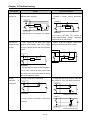
2) Output circuit wiring
PLC option card wiring method is as follows. Total four output terminals (Relay output) P40~P43 of
external terminal block (TB1) can be used.
5-4
24V
24 V 출력
Output
24GND
24GND
RS485(-)
(-) 단자
terminal
Modbus-RTU
Master
RS485
: Modbus-RTU
마스터
RS485 (+)
(+) terminal
Modbus-RTU
Master
RS485
단자 : Modbus-RTU
마스터
6 terminal inputs
4 terminal outputs
Chapter 5 Input and Output Function
Load
5-5
Chapter 6 Usage of Various Functions
Chapter 6 Usage of Various Functions
6.1 Built-in Functions
6.1.1 Pulse Catch Function
In the main unit, 6 points (P0000~P0005) of pulse catch input contact points are internalized.
Through using this contact point, 150 μs, short pulse signal, can be taken which can not be
executed by general digital input.
1) Usage
When narrow width of pulse signal is input, a trouble occurs which can not be detected by
general digital input, so the operation does not perform as user's intention. But in this
case through pulse catch function even narrow interval of pulse signal as 150 ㎲ min.
can be detected.
2) Minimum input pulse width.
P0000 ~ P0005 : 150μs
3) Operating Explanation
Input signal
Input image data
Scan 1
Step
Scan 2
Scan 3
Executing Contents
scan1
CPU senses input when pulse signal, min. 150 ㎲, is input, then saves the status.
scan2
used to turn on the region of input image
scan3
used to turn off the region of input image
4) Using Method
(1) Click the basic parameter twice on the project window of KGLMIN
(2) Select no. to use for pulse catch input of the basic parameter window.
For details of KGLWIN refers to the manual.
6-1
Chapter 6 Usage of Various Functions
Remark
1) Pulse catch input contact points operate as general digital input if they are not designated
as pulse catch input.
2) Pulse catch input contact points can be used 6 points from P000 to P005.
6-2
Chapter 6 Usage of Various Functions
6.1.2
Input Filter function
External input of PLC option card selects Input Filter Time from the range of 0-1000ms of
KGLWIN. Credibility secured system may be established by adjustment of input correction no.
through using environment
1) Usage
Input signal status affects the credibility of system in where noise occurs frequently or
pulse width of input signal affects as a crucial factor. In this case, the user sets up the
proper input on/off delay time, then the trouble by miss operation of input signal may be
prevented because the signal which is shorter than set up value is not adopted.
2) Operation
Input Filter Time
Input Signal
Input Image Data
Time
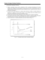
Input Signal
Input Image Data
The narrower width pulse than input filter time is not considered as input signal
3) Using method
(1) Click twice the basic parameter on the project window of KGLWIN.
(2) The value of filter can be set up as one of 1ms unit to the Input Filter Time of the
basic parameter window. (Input Filter Time is set up as default value of 10ms)
(3) Set up Input Filter Time is conformed to all input.
6-3
Chapter 6 Usage of Various Functions
6.1.3 External Interrupt Function
PLC option card for iS7 inverter Series can perform 6 points of external contact interrupt by
using input of main unit without special interrupt module.
1) Usage
This function is useful to execute a high speed execution regardless of scan time.
2) External Interrupt processing time
ㆍ P0 ~ P5 : 10μs
Remark
-. Above Interrupt processing time not include the program processing time of
external interrupt itself. It can be delayed by the processing time of interrupt
program.
3) Operation Explanation
External input signal
Scan program
In case of occurrence of
external interrupt signal
pause being executed scan
program and process
interrupt program.
Scan program
External contact
interrupt
program
End the interrupt
program process then
resume to execute
scan program.
4) Function
(1) Max. 6 points can be used to external interrupt input within P000 ~ P005.
(2) The number of external interrupt can be set max. 6. Namely, the number of external interrupt
is decreased by Time-driven Interrupt.
(3) The execution conditions of external interrupt is divided into following 3 kinds.
- Rising edge : Interrupt occurs at rising edge of external Interrupt contact point.
- Falling edge : Interrupt occurs at falling edge of external Interrupt contact point.
- Rising & falling edge : Interrupt occurs at both edges of external Interrupt contact point.
6-4
Chapter 6 Usage of Various Functions
5) Usage
(1) Click twice the parameter on the project window of KGLWIN.
(2) Designate contact point, no. of priority and movement condition of the task program which is
moved by interrupt inputting.
Time driven Interrupt
execution periodic set
Interrupt Type Setting
Interrupt input executing
condition
◎ Rising
◎ Falling
◎ Rising/Falling
Time driven Interrupt
execution periodic set
For the details , refer to KGLWIN manual.
6-5
Chapter 6 Usage of Various Functions
6.1.4 PID Control Function
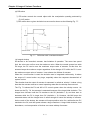
1) Introduction
This chapter will provide information about the built-in PID (Proportional Integral
Derivative) function of PLC option card of iS7 inverter series. The PID control means a
control action in order to keep the object at a set value (SV). It compares the SV with a
sensor measured value (PV : Present Value) and when a difference between them (E :
the deviation) is detected, the controller output the manipulate value (MV) to the actuator
to eliminate the difference. The PID control consists of three control actions that are
proportional (P), integral (I), and derivative (D).
Manual MV
Set Value
Present Value
MV
SV
PID
calculation
Manipulation
value
D/A
Automated MV
converting
module
Control
object
PV
A/D
converting
Sensor
The characteristics of the PID function of PLC option card for iS7 inverter is as following;
• The PID function is integrated into the CPU module.
• P operation, PI operation, PID operation and On/Off operation can be selected easily.
• PWM(Pulse Width Modulation) output is available.
• The manual output (the user-defined forced output) is available.
• By setting proper parameter, it can keep stable operation regardless of external
disturbance.
• The operation scan time (the interval that PID controller gets a sampling data from
actuator) is changeable for optimizing to the system characteristics.
• SV Ramp and Delta MV function are available.
6-6
Chapter 6 Usage of Various Functions
2) Specification
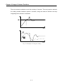
(a) Proportional Operation (P operation)
① P action means a control action that obtains a manipulate value which is
proportional to the deviation (E : the difference between SV and PV)
MV = K P × E
② The deviation (E) is obtained by difference between SV and PV and the formula of
deviation is as following;
MV = Kp × [SV − PV ]
where,
Kp: the proportional constant (gain),
SV: set value,
PV: present value
③ If the Kp is too large, the PV reaches to the SV swiftly, but it may cause a bad effect
like oscillations.
④ If the Kp is too small, oscillation will not occur. However, the PV reaches the SV
slowly and an offset may appear between PV and SV as shown in the Fig. 7.2.
⑤ The manipulation value (MV) varies from 0 to 4,000. User can define the maximum
value of MV (MV_MAX) and minimum value (MV_MIN) within the range 0 ~ 4,000.
⑥ When an offset remains after the system is stabilized, the PV can be reached to the
SV by adding a certain value. This value is called as bias value, and user can define
the bias value.
: Deviation
: Manipulating value
Deviation(E)
Manipulate value (MV)
Time
Fig 7.1 MV by P operation
: Kp is too large
PV
Oscillation
: Kp is too small
SV
Offset
Time
Fig. 7.2 The relation between Proportional constant (Kp) and present value (PV)
6-7
Chapter 6 Usage of Various Functions
(b) Integral Operation (I Operation)
① With integral operation, the manipulate value (MV) is increased or decreased
continuously in accordance time in order to eliminate the deviation between the SV
and PV. When the deviation is very small, the proportional operation can not produce
a proper manipulate value and an offset remains between PV and SV. The integral
operation can eliminate the offset value even the deviation is very small.
The period of the time from when the deviation has occurred in I action to when the
MV of I action become that of P action is called Integration time and represented as
Ti.
② Integral action when a constant deviation has occurred is shown as the following Fig.
7.3.
MV =
Kp
Edt
Ti ∫
As shown in the expression, Integral action can be made stronger or weaker by
adjusting integration time (Ti) in
I action. That is, the more the integration time (the
longer the integration time) as shown in Fig. 7.4, the less the quantity added to or
subtracted from the MV and the longer the time needed for the PV to reach the SV.
As shown in Fig. 7.5, when the integration time given is short, the PV will approach
the SV in short time since the quantity added or subtracted become increased. But, if
the integration time is too short, then oscillations occur, therefore, the proper P and I
value is requested.
③ Integral action is used in either PI action in which P action combines with I action or
PID action in which P and D actions combine with I action.
Fig. 7.3
The integral action with constant deviation
6-8
Chapter 6 Usage of Various Functions
It takes long time to
get the set value.
Fig. 7.4
The system response when a long integration time given
If the integration time is
too short, oscillations will
occur.
Fig. 2.6 The system response when a short integration time given
Fig. 7.5
The system response when a short integration time is given
6-9
Chapter 6 Usage of Various Functions
(c) Derivative operation (D action)
① When a deviation occurs, due to alteration of SV or external disturbances, D action
restrains the changes of the deviation by producing MV which is proportioned with the
change velocity (a velocity whose deviation changes at every constant interval) in order to
eliminate the deviation.
② D action gives quick response to control action and has an effect to reduce swiftly the
deviation by applying a large control action (in the direction that the deviation will be
eliminated) at the earlier time that the deviation occurs.
③ D action can prevent the large changes of control object due to external conditions.
④ The period of time from when the deviation has occurred to when the MV of D action
becomes the MV of P action is called derivative time and is represented as Td.
⑤ The D action when a constant deviation occurred is shown as Fig. 7.6
Fig. 7.6
Derivative action with a constant deviation
6-10
Chapter 6 Usage of Various Functions
(d) PID action
① PID action controls the control object with the manipulation quantity produced by
(P+I+D) action.
② PID action when a given deviation has occurred is shown as the following Fig. 7.7.
Fig. 7.7
PID action with a constant deviation
(e) Integral windup
All devices to be controlled, actuator, has limitation of operation. The motor has speed
limit, the valve can not flow over the maximum value. When the control system has wide
PV range, the PV can be over the maximum output value of actuator. At this time, the
actuator keeps the maximum output regardless of the change of PV while the PV is over
the maximum output value of actuator. It can shorten the lifetime of actuator.
When the I control action is used, the deviation term is integrated continuously. It makes
the output of I control action very large, especially when the response characteristic of
system is slow.
This situation that the output of actuator is saturated, is called as ‘windup’. It takes a long
time that the actuator returns to normal operating state after the windup was occurred.
The Fig. 7.8 shows the PV and MV of PI control system when the windup occurs. As
shown as the Fig. 7.8, the actuator is saturated because of the large initial deviation. The
integral term increase until the PV reaches to the SV (deviation = 0), and then start to
decrease while the PV is larger than SV (deviation < 0). However, the MV keeps the
saturated status until the integral term is small enough to cancel the windup of actuator.
As the result of the windup, the actuator will output positive value for a while after the PV
reached to the SV, and the system shows a large overshoot. A large initial deviation, load
disturbance, or miss-operation of devices can cause windup of actuator.
6-11
Chapter 6 Usage of Various Functions
There are several methods to avoid the windup of actuator. The most popular methods
are adding another feedback system to actuator, using the model of actuator and stop
integrating when actuator is saturated.
PV
SV
10
시간
Time
MV
Integral
Term
시간
Time
Fig. 7.8 Example of integral windup
6-12
Chapter 6 Usage of Various Functions
3) Realization of PID control on the PLC option card
In this chapter, it will describe how to get the digitized formula of the P, I, and D terms.
(a) P control
The digitized formula of P control is as following;
P (n) = K [SV (n) − PV (n)]
n : sampling number
K : proportional gain constant
b : reference value
SV : set value
PV : present value
(b) I control
The continuous formula of I control is as following;
I (t ) =
K
Ti
t
∫ e(s)ds
: integral term
0
K : proportional gain constant
Ti : integral time
e(s) : deviation value
By derivation about t, we can obtain;
dI K
= e
dt Ti
where, e = (SV – PV) : deviation value
The digitized formula is as following;
I (n + 1) − I (n) K
= e( n )
h
Ti
I (n + 1) = I (n) +
where,
h : sampling period
Kh
e( n )
Ti
(c) D control
The continuous formula of derivative term is as following;
Td d
dy
× D + D = − KTd
N dt
dt
N : high frequency noise depression ration
y : the object to be controlled (PV)
6-13
Chapter 6 Usage of Various Functions
4) Instruction and Parameter Setting
For the PID operation of PLC option card, following 2 instruction are included in the
KGLWIN software.
No.
Name
Description
1
PID8
Perform the PID operation
2
PID8AT
Perform the auto tuning operation
(a) PID8 instruction parameter setting and explanation.
(1) Scan Time
Scan time is the period of reading data (sampling), and also 10 times scaled up.
The range of sampling time is 0.1 ~ 10 seconds, and actual input range is 0 ~ 100.
Generally, scan time of Digital PID control should be less than 1/10 of time constant
of system response for better performance. Time constant is the time taken the
system’s step response reaches to the 63% of steady state.
(2) Operation Mode
Select automatic or manual operating mode. (Setting range: 0, 1 or D area)
(3) Manual Operate range
When manual operation is designates , manual operation value designates.
(input range : 0 ~ 4000)
(4) Output Limit Value
Designates minimum and maximum values of available manipulate value.
(range : 0 ~ 4000)
6-14
Chapter 6 Usage of Various Functions
(5) High Frequency Noise Depression Ratio
High frequency noise removal ratio is used for derivative control operation, and shows
the ratio of high frequency noise depression. If there is a lot of high frequency noise in
the control system, select the value as higher value.
Otherwise, leave the 1. The range of parameter is 0 ~ 10 and it is not scaled up, so
input the designated value directly. (it is possible that parameter value designates ‘D’
area also)
(6) Proportional gain
It is the ratio of proportional operation. Proportional gain is the 100 times scaled up
value. (Setting range: 1~10000)
(7) Derivative time and integral time
I_TIME and D_TIME are 10 times scaled up. For example, input 18894 if the
designated I_TIME value is 1889.4. The range of actual input is 0 ~ 20000. (it is
possible that parameter value designates ‘D’ area also)
(8) Mode command set (P, I, D control)
Following 7 operation modes are available.
No.
1
2
3
4
5
6
EN_P
EN_I
EN_D
PWM output
Operation
1(Enable)
0(Disable)
0(Disable)
0(Disable)
P operation
1(Enable)
1(Enable)
0(Disable)
0(Disable)
PI operation
1(Enable)
1(Enable)
1(Enable)
0(Disable)
PID operation
1(Enable)
0(Disable)
0(Disable)
1(Enable)
P operation/PWM output
1(Enable)
1(Enable)
0(Disable)
1(Enable)
PI operation/PWM output
1(Enable)
1(Enable)
1(Enable)
1(Enable)
PID operation/PWM output
7
On/Off operation
0(Disable)
0(Disable)
0(Disable)
0(Disable)
• Other operation modes, such as PD or I, are not permitted..
• If PWM output is selected, Manupulated value is outputted PWM output to designated output.
(9) PWM set
PWM(Pulse Width Modulation) is a output method which changes on-off duty of output
pulses by calculated manipulation value. Fig 7.9 shows example of PWM output.
Using PWM output, PID control system can be constructed easily without D/A
conversion module and power regulator.
When PWM is designates , ‘scan time’ item is disabled and ‘PWM’ items can be
designated. In this case, scan time is set to designated PWM output period. The range
of PWM output period is 1 ~ 10 seconds, and actual input range is 10 ~ 100. PWM
output point is only available for output contact of main unit.
6-15
Chapter 6 Usage of Various Functions
(10) Bias
The Bias data is used for the compensation of offset in the proportional control. The
range of input is 0 ~ 4000 or D area.
Be cautious that The actual range of Bias is –2000 ~ 2000. namely, 0~2000
represents 0 ~ +2000 and 2001 ~ 4000 represents -1 ~ -2000.
Example>
If offset(SV-PV) is 100 → Bias should be 100.
If offset(SV-PV) is -100 → Bias should be 2100.
(11) SV (Setting Value), PV(Present Value)
SV (setting value : the designated value) and PV (process value : present value) of
PID operation have the range 0 ~ 4000. The range can be set with the value of
data register. (Present value only can be set by data register.) Setting value means
the designated value to control and present value means the current value of
controlled device from sensor.
(12) PID algorithm
In PLC option card for iS7 inverter, two types of PID algorithm are available. The
velocity form(Speed) and positioning form.
Velocity form(Speed) operates incremental manners. Namely, it calculates the
change(∆n) required from previous manipulate value(MVn-1), but positioning form
calculates an absolute manipulate value(MVn) every sampling steps. Generally,
The velocity form is suited for the system in which load change is slow like
temperature control system, and positioning form is useful for system which’s load
change is fast.
(b) PID8AT instruction parameter setting and explanation.
(1) Scan time
S_TIME is the period of reading data (sampling), and 10 times scaled up for more
precious operation. The range of sampling time is 0.1 ~ 10 seconds, and actual input
range is 0 ~ 100.
6-16
Chapter 6 Usage of Various Functions
(2) Setting Value, Process Value
SV (set value : the designated value) and PV (process value : present value) of PID
operation have the range integer 0 ~ 4000. The range is set with the consideration of
the resolution of A/D and D/A module of PLC option card (12 bits) and offset value.
When setting the SV or PV, please be careful when converting the analog value of
control object (temperature, velocity, etc.) to digital value that are the output of A/D
convert module.
(3) Tuning method
The PLC option card for iS7 inverter perform auto-tuning operation in two methods.
One is relay response method and the other is process reaction curve method.
1) Relay response method
• PID parameters are obtained by On/Off operation during 1 cycle of PV variation.
• PID parameters are obtained by amplitude and period of oscillation
• The On/Off operation will occur at the SV value.
MV
Period
SV
Amplitude
2) Process reaction curve method(PRC method).
• PID parameters are obtained by step response of process.
• It is useful fo r time 1st order time delay system expressed as following
K
e − Ls
Ts + 1
• Obtained parameters may not accurate if the process can’t approximated to 1st
order system, In this case, use relay response method.
Time delay(L)
4000
MV
80% of SV
63% of SV
Time
6-17
Chapter 6 Usage of Various Functions
5) Instruction
(1) PID8
Available device
Flag
Instruction
No. of
M
P
K
L
F
T
C
S
D
n
O
S1
O
#
D
integer
Steps
Error
(F110)
5
O
Zero
(F111)
Carry
(F112)
O
PID8
Flag Set
Error
(F110)
PID8
n
S1
Error flag turns on when designating
area is over and the instruction isn’t
executed.
Designation
n
Registration No. at parameter(0~7)
S1
Execution status registration area
■ PID8 (PID operation)
a) Usage
• When the condition of execution is on, PID operation executes.
• ‘n’ is registration No.at parameter( 0 ~ 7)
b) Example Program
• When the input condition M0 turns on, PID operation executes at no.2 parameter.
• PID execution status registrates D0000 and the output value of control result registrates
D0001.
• If SV Ramp is designated, current SV is registrate D0005
bF bE bD bC bB bA b9 b8 b7 b6 b5 b4 b3 b2 b1 b0
D0000
Done : normal execution signal
6-18
Chapter 6 Usage of Various Functions
(2) PID8AT
Available device
Flag
No. of
Instruction
M
PID8AT
P
K
L
F
T
C
S
D
n
O
S1
O
inte
ger
#
D
Steps
Error
(F110)
5
O
O
Zero
(F111)
Carry
(F112)
Flag Set
PID8AT
n
Error
(F110)
S1
Error flag turns on when designating
area is over and the instruction isn’t
executed.
Designation
n
Registration No. at parameter(0~7)
S1
Execution status registration area
■ PID8AT (Auto-tuning by parameter)
a) Usage
• When the condition of execution is on, PID auto tuning operation executes and calculates
P,I,D constant.
• ‘n’ is registration No.at parameter( 0 ~ 7)
• S1 is execution status and P,I,D constant registration area.
b) Example program
• When the input condition M0 turns on, PID operation executes at no.2 parameter.
• PID execution status stores D0000 and the output value of control result stores D0001
and P,I,D constant sequentially store D002(P),D003(I),D004(D).
bF bE bD bC bB bA b9 b8 b7 b6 b5 b4 b3 b2 b1 b0
D0000
Auto tuning end bit
Done : normal execution signal
6-19
Chapter 6 Usage of Various Functions
6) Example Program
(1) System Configuration
Expansion I/O or
Remote I/O
PLC option card for
iS7 inverter series
KGL-WIN
Above V 3.4
Present Value
(PV: DC4~20mA)
RS-232C
Signal Converter
Manipulated Value
Temp. Sensor
(MV: DC4~20mA)
Electric Oven
(0~200 ℃)
Heater
TPR
(2) Initial Setting
a) PID Control function (parameter setting by built-in function of PLC option card)
■ Operation Scan Time: set by 1 second (Setting value = 10)
■ Operation mode: Automatic setting
■ Output Limit Value: Max. = 4000, Min. = 0
■ Manipulated Value setting: Set by 0 (Automatic operation mode)
■ High Frequency Noise Removal setting: set by 10
■ Setting Value (when Resistor Thermal Detector sensor is used)
960(60 oC),1120(70 oC),1280(80 oC),1600(100 oC)
■ Current value setting: D4980
(Temporary D area to save the current temperature measured by temperature
sensor)
■ BIAS setting: 0 (If only P control is used, input proper value other 0)
■ P,I,D Algorithm setting: Select proper algorithm.
(If PWM output is needed, select related item)
■ PWM period, Contact Setting: In case of PWM output is set, input the proper
period and output relay value.
6-20
Chapter 6 Usage of Various Functions
b) Auto-tuning Control function
(parameter setting by built-in function of PLC option card)
■ Setting Value (when Resistor Thermal Detector sensor is used)
960(60 oC),1120(70 oC),1280(80 oC),1600(100 oC)
■ Operation Scan Time: Set by 1 second (Setting value = 10)
■ Present Value setting: D4980
(Temporary D area to save the current temperature measured by temperature
sensor)
■ Tuning method:
Relay response method
c) Remote I/O (A/D Converter)
■ Input range: DC 4~20 mA
■ Data saving area of converted value of A/D: D4980
d) Remote I/O (D/A Converter)
■ Output range: DC 4~20 mA
■ Data saving area of converted value of D/A: D4982
(3) Program Explanation
a) PID operation explanation (without Auto-tuning function)
• Measure current temperature (-200~600°C) by RTD module then digital conversion
value(0 ~ 4000) is stored to D4980
• PID8 instruction will calculate manipulate value (MV : 0 ~ 4000) based on PID
parameter settings (P_GAIN, I_TIME, D_TIME, etc.) and PV from RTD module.
Then, the calculated MV is output to the channel 0 of D/A module. (PID operation
Done bit: bit0)
• D/A module will convert the MV to analog signal and output to the actuator (power
converter).
b)PID operation explanation (with A/T function)
• Measure current temperature (-200~600°C) by RTD module then digital
conversion value(0 ~ 4000) is stored to D4980
• PID8AT instruction will calculate manipulate value (MV : 0 ~ 4000) based on the
SV and PV from RTD module. Simultaneously, the PID8AT instruction will
calculate P,I and D parameters.
• The END bit of auto tuning status device will be 1 when the auto tuning is
completed. Then, PLC option card will start PID operation with PID parameters
that are calculated by Auto-tuning function.
6-21
Chapter 6 Usage of Various Functions
(4) Parameter Setting and Program
a) In case of using PID function only
When PWM set is selected, Scan
When PWM is designated, this window
time parameter is disabled and
is activated and PID function operates
this value is ignored.
by PWM period.
When M0 turns on,
PID operation executes at no.0
parameter.
When M0 turns off,
CPU stop PID operation
and output 0 to D/A.
module.
6-22
The manipulated value is
out to D/A module.
Chapter 6 Usage of Various Functions
b) In case of using combined function of PID operation and Auto tuning.
This program shows the PID operation with the Auto-tuning value of P, I, and D. After
Auto-tuning is completed, PID operation will start with calculated PID parameter
When RPC Method is
selected, the scan time
fixed to 1 sec.
As a result of PID8AT execution,
Proportional gain(P), Derivative
time(D), Integral time(I) are
stored D0102, D0103, D0104.
6-23
Chapter 6 Usage of Various Functions
When auto tuning ends at
D0010, M0001 turns on and
When M0000 turns on, auto
tuning starts.
Calculated P,I,D parameters are
saved to D0012, D0013, D0014.
PID control starts.
6-24
When
M0001
output 0 to D4982.
turns
off,
Chapter 7 Exclusive Functions for iS7 Inverter Control/Monitoring
Chapter 7 Exclusive Functions for iS7 Inverter Control/Monitoring
7.1 Outline and Installation
7.1.1 Outline and Major Components of the Product
SW1
LED1, LED2
CON1
Battery
Housing
J3
T/B 1
J2
Symbol
Name
Description
LED1
RUN LED
ON state: local run (SW1 is at RUN position) or remote run (SW1
is at PAU/REM position, and RUN icon is selected in KGLWIN)
LED2
ERR LED
1) Blink: flickers in error condition.
2) OFF: in normal condition for operation.
SW1
Mode Selection
Switch
1) RUN position: program running
2) PAU/REM position: pause, executing remote run/stop, etc.
3) STOP position: program stopped
1) The default jumper at product delivery. Only manufacturer’s A/S
personnel are allowed to change the default setting. Keep the
setting as shown below.
J1
J2
PLC OS Download
Jumper
Terminal Selection
Jumper
Normal
Mode
1) ON: select RS485 communication terminal resistance (internal
120ohm resistor).
2) OFF: do not select RS485 communication terminal resistance.
7-1
Chapter 7 Exclusive Functions for iS7 Inverter Control/Monitoring
Symbol
Name
Description
1) NPN mode: connects terminal block input (P00~P05) and 24G.
for details, see page 7-5.
Terminal
input acts
as NPN.
NPN/PNP Selection
Jumper
J3
2) PNP mode: connects terminal block input (P00~P05) and 24P.
for details, see page 7-5.
Terminal
input acts
as PNP.
CON1
RS232C
Communication
Connector
Battery
Battery Housing
TB1
External Terminal
Block
Connector for connection with KGLWIN
1) Function: in case of power failure, maintain the data of the latch
area of PLC option and RTC time data.
2) Battery type: coin-type lithium ion battery (CR2032)
3) Service life: approx. 4 years in power-off state (at room
temperature, battery capacity 220mAh)
1: S+(RS485)
2: S-(RS485)
3: 24G
4: Terminal input P00
5: Terminal input P01
6: Terminal input P02
7: Terminal input P03
8: Terminal input P04
9: Terminal input P05
10: 24G
11: 24P (external 24V output)
12: Terminal output P40
13: Terminal output P40C
14: Terminal output P41
15: Terminal output P41C
16: Terminal output P42
17: Terminal output P42C
18: Terminal output P43
19: Terminal output P43C
Detail outline of the external terminal block (TB1) is shown below.
7-2
24V Output
출력
24GND
24GND
RS485
: Modbus-RTU
마스터
RS485 (-)
(-) 단자
Terminal
: Modbus RTU
RS485
(+) Terminal
단자 : Modbus-RTU
마스터
RS485 (+)
: Modbus RTU
6 TB outputs
4 TB outputs
Chapter 7 Exclusive Functions for iS7 Inverter Control/Monitoring
7.1.2 Detail description of the components
(1) Mode Selection Switch (SW1 in the outline drawing)
The SW1 shown in the product outline drawing is for mode selection.
PLC Option
Settings of the Mode Selection Switch and KGLWIN
Operation Status
Local Run
1. Mode selection switch: RUN position
1. Mode selection switch: set to AU/REM position.
Run
Remote
2. Select the icon shown below (in the circle).
Run
Local Stop
1. Mode selection switch: STOP position
1. Mode selection switch: set to PAU/REM position.
Stop
Remote
2. Select the icon shown below (in the circle).
Stop
Local
1. Mode selection switch: move to PAU/REM position during Local run.
1. Mode selection switch: set to PAU/REM position.
Pause
Remote
2. Select the icon shown below (in the circle).
(2) Display LED (LED1, LED2 in the outline drawing)
LED1(RUN LED) and LED2(ERR LED) are designated in the outline drawing.
Classification
RUN LED
ERR LED
STOP Status
OFF
OFF
RUN Status
ON
OFF
Heavy Error
-
Light Error
-
Program Error
-
Error in communication
with the inverter (Note 1)
Remark
RUN LED remains ON,
not blinking
ON(100ms)/OFF(100m
See 10.5 Error Code
s), blinking
List.
ON(500ms)/OFF(500m
See 10.5 Error Code
s), blinking
List.
ON(1000ms)/OFF(1000
See 10.5 Error Code
ms), blinking
List.
ON(500ms)/OFF(500m
ON(500ms)/OFF(500m
RUN LED and ERR
s), blinking
s), blinking
LED blink at the same
intervals (500ms).
(Note 1)
the inverter and PLC option card maintain data communication. This error occurs if the inverter fails to
response to the PLC option card within specified time (approx. 300ms), due to an external cause such as
noise.
7-3
Chapter 7 Exclusive Functions for iS7 Inverter Control/Monitoring
(3) Serial (RS232C) Communication (CON1 in the outline drawing)
This part is designated with CON1 in the outline drawing.
In the RS232C used in this PLC option, No. 2 and No.3 lines are cross-linked as shown below, while No.
5 is interconnected.
1) For KGLWIN download
User can download the ladder program made out in the KGLWIN.
The related jumper is J1, which must be set up as shown below (default set position)
Normal
Mode
2) For CPU OS download (please contact A/S center if you have to change the setting)
This function is not available for users. Contact our A/S center.
Download
Caution! User must not make the
mode
setting shown in the left!
(4) RS485 (Modbus-RTU Protocol: Master) Communication (S+ and S- terminals of the
TB1 in the outline drawing)
In the product outline drawing, the S+ (RS485 + terminal) and S-terminal (RS485 –terminal) of the TB1
(external terminal block.
RS485 (-) Terminal: Modbus-RTU Master
RS485 (+) Terminal: Modbus-RTU Master
The standard Modbus-RTU protocol is supported in this product, and it is the master protocol. The
Remote I/O, inverter, etc., built-in with Modbus-RTU (Slave) can be configured as the lower level.
7-4
Chapter 7 Exclusive Functions for iS7 Inverter Control/Monitoring
(5) Terminal input (P00~P05 terminals of TB1 in the drawing)
Total 6 terminal inputs are supported from P00~P05 on the external terminal block (TB1).
◆ NPN (Sink) mode
1) Set the J3 (NPN/PNP selection jumper) as shown below.
Terminal
inputs are in
NPN mode
2) Connect the wires to the external terminal block (TB1). The figure below shows PO connection only
for convenience (same for P1~P5 terminals).
External Switch
◆ PNP (Source) Mode
1) Set up the J3 (NPN/PNP selection jumper) as shown below.
Terminal
inputs are in
PNP mode.
2) Connect the wires to TB1 as shown below. As illustrated, this product provides a 24V output from
the terminal block. In the figure below, the 24V output is used for PO connection (same for the P1~P5
terminals).
External Switch
7-5
Chapter 7 Exclusive Functions for iS7 Inverter Control/Monitoring
(6) Terminal output (P40~P43 terminals of TB1 in the outline drawing)
This product provides total 4 terminal output contacts (4 relay contacts) which are P40~P43 on the TB1.
Connection method is as shown below.
Load
1) Output functions of PLC option under inverter LV (low voltage) trip (default)
When the iS7 inverter is tripped by LV(low voltage), the contacts which have been ON remain the
ON status.
When the iS7 inverter is fully discharged and the power supply to the control board of this product is
cut-off, the outputs from the contact points become OFF. (Note: larger iS7 inverter capacity gives
longer time from LV trip to power supply cut-off to the control board).
The above describes the default specifications of this product.
2) Output functions of PLC option under inverter LV (low voltage) trip (application)
If the inverter has large capacity, the time elapsed form the inverter’s LV trip to the power supply to
the control board of this product is cut-off is relatively long, e.g., 10 or more seconds. Therefore,
according to the requirement of the installation, the output contacts of this product may have to be
isolated before the said time. The method of cutting off the output of this product at the time of LV
trip of inverter is described in page 7-27~28.
(7) Terminal resistance for RS485 communication (J2 in the outline drawing)
If the J2 jumper is set to ON, terminal resistance of 120 ohm is inserted between the internal
communication (Modbus-RTU) lines (S+, S-). When this product is installed at the terminal of a
communication system, set the terminal resistance jumper J2 to ON. This will adjust the impedance
between the communication lines to improve the distortion and attenuation of the RS485 communication
signals caused by the delay in data transmission.
7-6
Chapter 7 Exclusive Functions for iS7 Inverter Control/Monitoring
(8) Battery Housing
1) Battery specification
Coin-type, lithium ion battery (Type: CR2032).
2) Service life of battery
A new battery (capacity 220mAh, at 20℃) can supply power to this product for about 4 years without
external power supply. When the external power supply is ON, the battery is not discharged.
3) Data maintained by battery power during external power failure
- all the data in the latch area set up by KGLWIN
- clock data (internal RTC)
4) Battery discharge check
Turn on the power of this product. Go to No. 73 (Real Time) in the CNF group of the iS7 inverter using
the loader of the iS7. If the present time is “2000/01/01 00:00,” the battery needs to be replaced.
The same will be displayed at power turn OFF/ON if no battery is installed.
5) Battery replacement
- Turn the power supply of the iS7 inverter to OFF.
- Remove iS7 inverter cover. Remove the cover of this product, too.
- Remove discharged battery carefully.
- Insert a new battery and push it down with a thumb.
- Turn on the power of the iS7 inverter.
- Connect CON1 with the RS232C cable. In the KGLWIN menu, select “Online Æ Write Data Æ Clock
Data.” Enter present time and check that the time displayed on the CNF73(Real Time) is correct.
7-7
Chapter 7 Exclusive Functions for iS7 Inverter Control/Monitoring
7.2 Functions of PLC Option Card exclusively for iS7 Inverter
7.2.1 List of the special D registers for iS7 inverter control and monitoring
Classific
ation
Area
D4454
Description
Ref. Page
Using the digital loader of the inverter, register the addresses
D4455 (see Appendix, page 4, App. 4-6, 4-7) of the parameters (max. 8)
D4456 of the common area of the inverter, which will be controlled by the
D4457
Control
D4458
PLC option card, in the APO60~67 (PLC Wr Data 1~8). These
inverter parameters corresponding to the registered addresses 7-11 ~ 7-17
(max. 8) can be modified by writing specific values in the special
D4459 area registers (D4454:APO60, D4455:APO61, D4456:APO62,
D4460 D4457:APO63, D4458:APO64, D4459:APO65, D4460:APO66,
D4461 D4461:APO67) allocated to each parameter.
D4474
Using the digital loader of the inverter, register the addresses
D4475 (see Appendix, page 4, App. 4-1, 4-5) of the parameters (max. 8)
D4476 of the common area of the inverter, which will be controlled by the
D4477
D4478
D4479
Monitoring
PLC option card, in the APO76~83 (PLC Rd Data 1~8).
Read the inverter parameters in the addresses (max. 8) and write 7-18 ~ 7-24
them in the PLC special area registers (D4474:APO76,
D4475:APO77, D4476:APO78, D4477:APO79, D4478:APO80,
D4480 D4479:APO81, D4480:APO82, D4481:APO83) allocated to each
D4481 of them.
D4490 iS7 Inverter Trip Information -1
D4491 iS7 Inverter Trip Information -2
D4492 iS7 Inverter Trip Information -3
D4493 iS7 Inverter Trip Information -4
7-8
7-25 ~ 7-26
Chapter 7 Exclusive Functions for iS7 Inverter Control/Monitoring
7.2.2 Control (PLC Option Æ Inverter)
(1) iS7 Inverter Frequency Reference
PLC option can change the inverter’s frequency reference. Here, the DRV07 (Freq Ref Src) must be se to
“PLC.”
▶ Common area of the iS7 inverter
Referring to the parameters (exclusively for control) of inverter common area in the “App. 4-6, page 4,
Appendix,” the addresses of the common area of the inverter frequency reference are as follows.
Common Area Address
Name
Remark
0x380
Inverter Command Freq.
Common Area (Write) address for iS7
▶ Special D registers of PLC for inverter control corresponding to APO60 ~ 67
Register
D4454
D4455
D4456
D4457
D4458
D4459
D4460
D4461
Use of the Register
Data to be inputted in the common area parameter
address set up by APO60 (PLC Wr Data1)
Data to be inputted in the common area parameter
address set up by APO61 (PLC Wr Data2)
Data to be inputted in the common area parameter
address set up by APO62 (PLC Wr Data3)
Data to be inputted in the common area parameter
address set up by APO63 (PLC Wr Data4)
Data to be inputted in the common area parameter
address set up by APO64 (PLC Wr Data5)
Data to be inputted in the common area parameter
address set up by APO65 (PLC Wr Data6)
Data to be inputted in the common area parameter
address set up by APO66 (PLC Wr Data7)
Data to be inputted in the common area parameter
address set up by APO67 (PLC Wr Data8)
Remark
PLC
OptionÆInverter(control)
PLC
OptionÆInverter(control)
PLC
OptionÆInverter(control)
PLC
OptionÆInverter(control)
PLC
OptionÆInverter(control)
PLC
OptionÆInverter(control)
PLC
OptionÆInverter(control)
PLC
OptionÆInverter(control)
▶ Application and exemplary program
1) Set up the inverter parameters as shown below. In the APO60(PLC Wr Data1), enter the “0380Hex”
which is the address (page 4, “App. 4-6, Appendix) of the common area of the inverter frequency
reference.
Code
Function Name
Setting Value
DRV07
Freq Ref Src
PLC
APO60
PLC Wr Data1
0380 Hex
2) APO60 (PLC Wr Data1) corresponds with D4454 which is the special register of the PLC option by 1:1
relation. Since the APO60 (PLC Wr Data1) is registered with the common area address (0380Hex) of the
inverter frequency reference, a specific value inputted in the D4454 in ladder program, the value will be
the frequency reference of the inverter.
In the sample ladder program below, if the contact point of the M0000 is ON, the inverter will be set up
with the frequency reference of 37.00Hz.
7-9
Chapter 7 Exclusive Functions for iS7 Inverter Control/Monitoring
(2) iS7 Inverter Operation Reference
PLC option can provide operation reference to an inverter.
▶ Common area of inverter
Referring to the parameters (exclusively for control) of inverter common area in the “App. 4-6, page 4,
Appendix,” the addresses of the common area of the inverter operation reference are as follows.
Common Area
Address
0x0382
Function
Detailed Description
Inverter Run Command
BIT0
0: Stop command 1: Run command
BIT1
0: Reverse operation
1: Forward operation
BIT2
0Æ1 : Fault Reset
BIT3
0Æ1 : Free-run to stop
1Æ0: Fault reset of Free-run to stop
▶ Special D registers of PLC for inverter control corresponding to APO60 ~ 67
Register
D4454
D4455
D4456
D4457
D4458
D4459
D4460
D4461
Use of the Register
Data to be inputted in the common area parameter
address set up by APO60 (PLC Wr Data1)
Data to be inputted in the common area parameter
address set up by APO61 (PLC Wr Data2)
Data to be inputted in the common area parameter
address set up by APO62 (PLC Wr Data3)
Data to be inputted in the common area parameter
address set up by APO63 (PLC Wr Data4)
Data to be inputted in the common area parameter
address set up by APO64 (PLC Wr Data5)
Data to be inputted in the common area parameter
address set up by APO65 (PLC Wr Data6)
Data to be inputted in the common area parameter
address set up by APO66 (PLC Wr Data7)
Data to be inputted in the common area parameter
address set up by APO67 (PLC Wr Data8)
Remark
PLC
OptionÆInverter(control)
PLC
OptionÆInverter(control)
PLC
OptionÆInverter(control)
PLC
OptionÆInverter(control)
PLC
OptionÆInverter(control)
PLC
OptionÆInverter(control)
PLC
OptionÆInverter(control)
PLC
OptionÆInverter(control)
▶ Application and exemplary program
1) 1) Set up the inverter parameters as shown below. In the APO60(PLC Wr Data1), enter the
“0382Hex” which is the address (page 4, “App. 4-6, Appendix) of the common area of the inverter
operation reference.
Code
Function Name
Set Value
DRV01
Cmd Frequency
11.52 Hz
DRV06
Cmd Source
PLC
DRV07
Freq Ref Src
Keypad-1
APO60
PLC Wr Data1
0382 Hex
2) APO60 (PLC Wr Data1) corresponds with D4454 which is the special register of the PLC option by 1:1
relation. Since the APO60 (PLC Wr Data1) is registered with the common area address (0382Hex) of the
inverter operation reference, a specific value inputted in the D4454 in ladder program, the value will be
the operation reference of the inverter.
7-10
Chapter 7 Exclusive Functions for iS7 Inverter Control/Monitoring
3) In the ladder program below, when the M0002 contact is ON, the inverter operates forward at the
frequency of 11.52Hz (frequency 11.52Hz reference from keypad).
(3) Using inverter digital output contact points (basic 10: 3 points, with 10 extensions: basic
10 + 3 points) as the digital output contact points of PLC option.
◎ Number of output contact points (iS7 internal output points + extended IO output points)
Type
Number of Digital Output points
Basic I/O/O
2 points (Relay output)+1point (TR output)
Expansion I/O
3points (Relay output)
Total points
6 points
The digital output points (relay output contact points) of PLC option is 4 points. If more digital output points
are required, you can make use of extended digital output points (3 relay output points) in addition to the
points (2 relay points, 1 TR points) built in the inverter. In detail, in addition to the 4 basic digital output points
(relay outputs) built-in the PLC option card, 6 output points (9 relay points, 1 TR point) comprising the 3 basic
digital output points (2 relay points, 1 TR point) built-in the iS7 inverter and the 3 relay output points of the
extension I/O board are available for the PLC option.
▶ Inverter parameter setting
The inverter digital output to be used by the PLC option must be set to “None.”
Code
Function Name
Set Value
OUT31
Relay 1
None
OUT32
Relay 2
None
OUT33
Q1
None
▶ Common area of inverter
Referring to the parameters (exclusively for control) of inverter common area in the “App. 4-6, page 4,
Appendix,” the addresses of the common area of the inverter’s digital outputs are as follows.
Common Area
Address
0x0386
Function
Inverter Digital
Output
Detailed Description
BIT0
0: Relay1 OFF
1: Relay1 ON
BIT1
0: Relay2 OFF
1: Relay2 ON
BIT2
0: Q1 OFF
1: Q1 ON
BIT3
0: Q2 OFF
1: Q2 ON
BIT4
0: Q3 OFF
1: Q3 ON
BIT5
0: Q4 OFF
1: Q4 ON
7-11
Remark
0x0386
Chapter 7 Exclusive Functions for iS7 Inverter Control/Monitoring
▶ Special D registers of PLC for inverter control corresponding to APO60 ~ 67
Register
D4454
D4455
D4456
D4457
D4458
D4459
D4460
D4461
Use of the Register
Remark
Data to inputted in the common area parameter
address set up by AP060 (PLC Wr Data 1).
Data to inputted in the common area parameter
address set up by AP061 (PLC Wr Data 2).
Data to inputted in the common area parameter
address set up by AP062 (PLC Wr Data 3).
Data to inputted in the common area parameter
address set up by AP063 (PLC Wr Data 4).
PLC option → Inverter
(Control)
PLC option → Inverter
(Control)
PLC option → Inverter
(Control)
PLC option → Inverter
(Control)
Data to inputted in the common area parameter
address set up by AP064 (PLC Wr Data 5).
Data to inputted in the common area parameter
address set up by AP065 (PLC Wr Data 6).
Data to inputted in the common area parameter
address set up by AP066 (PLC Wr Data 7).
Data to inputted in the common area parameter
address set up by AP067 (PLC Wr Data 8).
PLC option → Inverter
(Control)
PLC option → Inverter
(Control)
PLC option → Inverter
(Control)
PLC option → Inverter
(Control)
▶ Application and exemplary program
1) Set up the inverter parameters as follows. In the APO60 (PLC Wr Data1), enter 0386Hex which is the
common area address of the inverter digital output (page 4, “App. 4-6, Appendix).
Code
Function Name
Set Value
OUT31
Relay 1
None
OUT32
Relay 2
None
APO60
PLC Wr Data1
0386 Hex
2) APO60 (PLC Wr Data1) corresponds with the D4454 which is the special register of PLC option by 1:1
relation. Since the APO60 (PLC Wr Data1) is currently registered with the common area address
(0386Hex) of the virtual multi-function output of the inverter, if a specific value is entered in the D4454 by
the ladder program, the value will be the digital output of the inverter.
3) In the sample program below, if D4454 is written with h0003, 30A-30C of Relay1 and AXA-AXC of
Relay2 are short-circuited. And then, if D4454 is written with h0000, the 30A-30C and AXA-AXC of
Relay2 are opened.
7-12
Chapter 7 Exclusive Functions for iS7 Inverter Control/Monitoring
(4) Writing other common area parameters frequently used
(e.g.: acceleration and deceleration times, etc.)
PLC option can write all the common area parameters of inverter.
In this manual, PLC option will set up (write) acceleration and deceleration times.
▶ Inverter common area
Referring to the parameters (exclusively for control) of inverter common area in the “App. 4-6, page 4,
Appendix,” the addresses of the common area of the inverter acceleration and deceleration time are as
follows.
Common Area
Function
Detailed Description
0x0383
Acceleration Time
Setting of Acceleration Time
0x0384
Deceleration Time
Setting of Deceleration TIme
Address
▶ Special D registers of PLC for inverter control corresponding to APO60 ~ 67
Register
D4454
D4455
D4456
D4457
D4458
D4459
D4460
D4461
Use of the Register
Data to inputted in the common area parameter
address set up by AP060 (PLC Wr Data 1).
Data to inputted in the common area parameter
address set up by AP061 (PLC Wr Data 2).
Data to inputted in the common area parameter
address set up by AP062 (PLC Wr Data 3).
Data to inputted in the common area parameter
address set up by AP063 (PLC Wr Data 4).
Data to inputted in the common area parameter
address set up by AP064 (PLC Wr Data 5).
Data to inputted in the common area parameter
address set up by AP065 (PLC Wr Data 6).
Data to inputted in the common area parameter
address set up by AP066 (PLC Wr Data 7).
Data to inputted in the common area parameter
address set up by AP067 (PLC Wr Data 8).
Remark
PLC option →Inverter (Control)
PLC option →Inverter (Control)
PLC option → Inverter (Control)
PLC option → Inverter (Control)
PLC option → Inverter (Control)
PLC option → Inverter (Control)
PLC option → Inverter (Control)
PLC option → Inverter (Control)
▶ Application and exemplary program
1) Set up inverter parameters as follows; in the APO60 (PLC Wr Data1), enter 0383Hex which is the
common area address (page 4, “App. 4-6, Appendix) of inverter acceleration time, and in the APO61
(PLC Wr Data2), enter 0384Hex which is the common area address (page 4, “App. 4-6, Appendix) of
inverter deceleration time.
Code
APO60
APO61
Function Name
Set Value
PLC Wr Data1
0383 Hex
PLC Wr Data2
0384 Hex
7-13
Chapter 7 Exclusive Functions for iS7 Inverter Control/Monitoring
3) The APO60 (PLC Wr Data1) and APO61 (PLC Wr Data2) correspond to D4454 and D4455 which are
the special registers of PLC option, respectively, by 1:1 relation.
Because, the APO60 (PLC Wr Data1) and APO61 (PLC Wr Data2) are registered with the common
area address (0383Hex) of inverter acceleration time and the common area address (0384Hex) of
inverter deceleration time, respectively, if a specific value is entered in D4454 or D4455, the value will be
inverter’s acceleration or deceleration time, respectively.
2) When the sample program below is executed, inverter acceleration time (DRV03:Acc Time) will be
changed to 12.5sec and the deceleration time (DRV04:Dec Time) will be changed to 14.3sec.
7-14
Chapter 7 Exclusive Functions for iS7 Inverter Control/Monitoring
7.2.3 Monitoring (PLC Option Í Inverter)
(1) Using inverter digital input points as the digital input points of PLC option
Maximum 11 digital input points of inverter (with basic 10 points mounted: 8 points, with 10 extension points:
basic 10 + 3 points) can be used as the digital input points of PLC option. Or, the status (0 or 1) of inverter
digital input points can be used simply for monitoring function.
▶ Common area of inverter
Referring to the parameters (exclusively for monitoring) of inverter common area in the “App. 4-2, page 4,
Appendix,” the addresses of the common area of the inverter digital input status are as follows.
Common Area
Address
0320 Hex
Function
Information of
Inverter Digital
Input Point
Detailed Description
Remark
BIT0
BIT1
BIT2
BIT3
BIT4
BIT5
BIT6
BIT7
0: P1 OFF
0: P2 OFF
0: P3 OFF
0: P4 OFF
0: P5 OFF
0: P6 OFF
0: P7 OFF
0: P8 OFF
1: P1 ON
1: P2 ON
1: P3 ON
1: P4 ON
1: P5 ON
1: P6 ON
1: P7 ON
1: P8 ON
BIT8
0: P9 OFF
1: P9 ON
BIT9
0: P10 OFF
1: P10 ON
BIT10
0: P11 OFF
1: P11 ON
Built-in (IN65)
Built-in (IN66)
Built-in (IN67)
Built-in (IN68)
Built-in (IN69)
Built-in (IN70)
Built-in (IN71)
Built-in (IN72)
In case expansion I/O is
installed (IN73)
In case expansion I/O is
installed (IN74)
In case expansion I/O is
installed (IN75)
▶ Special D registers of PLC for inverter status monitoring corresponding to APO76 ~ 83
Register
D4474
D4475
D4476
D4477
D4478
D4479
D4480
D4481
Use of the Register
Data of common area parameter address is
saved set up by APO76 (PLC Rd Data1).
Data of common area parameter address is
saved set up by APO77 (PLC Rd Data2).
Data of common area parameter address is
saved set up by APO78 (PLC Rd Data3).
Data of common area parameter address is
saved set up by APO79 (PLC Rd Data4).
Data of common area parameter address is
saved set up by APO80 (PLC Rd Data5).
Data of common area parameter address is
saved set up by APO81 (PLC Rd Data6).
Data of common area parameter address is
saved set up by APO82 (PLC Rd Data7).
Data of common area parameter address is
saved set up by APO83 (PLC Rd Data8).
Remark
Inverter → PLC option
(Monitoring)
Inverter → PLC option
(Monitoring)
Inverter → PLC option
(Monitoring)
Inverter →PLC option
(Monitoring)
Inverter → PLC option
(Monitoring)
Inverter → PLC option
(Monitoring)
Inverter → PLC option
(Monitoring)
Inverter →PLC option
(Monitoring)
▶ Application and exemplary program
1) Set up inverter parameters as follows. Especially, enter 320Hex which is the inverter digital input
status address (App. 4-2. page 4, Appendix) in the APO76 (PLC Rd Data1).
Code
Function Name
Set Value
APO76
PLC Rd Data1
0320 Hex
7-15
Chapter 7 Exclusive Functions for iS7 Inverter Control/Monitoring
2) The APO76 (PLC Rd Data1) corresponds by 1:1 with the D4474 which is the special register of PLC
option. Therefore, the value in the D4474 is the data (inverter digital input status) stored in the
0320Hex which is the address of the inverter digital input status registered in the APO76 (PLC Rd
Data1).
3) For an example with the ladder program below, PLC option can monitor the digital input status (0 or
1) of the inverter.
Status of P1 (IN65):
0 (Off), 1 (On)
Status of P2 (IN66):
0 (Off), 1 (On)
Status of P8 (IN72):
0 (Off), 1 (On)
4) When the inverter’s multifunction input P1 is ON, the P0062 coil is excited as shown below.
Status of P1 (IN65):
0 (Off), 1 (On)
Status of P2 (IN66):
0 (Off), 1 (On)
Status of P8 (IN72):
0 (Off), 1 (On)
5) When the inverter’s multifunction input P2 is ON, the P0063 coil is excited as shown below.
Status of P1 (IN65):
0 (Off), 1 (On)
Status of P2 (IN66):
0 (Off), 1 (On)
Status of P8 (IN72):
0 (Off), 1 (On)
6) When the inverter’s multifunction input P8 is ON, the P0064 coil is excited as shown below.
Status of P1 (IN65):
0 (Off), 1 (On)
Status of P2 (IN66):
0 (Off), 1 (On)
Status of P8 (IN72):
0 (Off), 1 (On)
Caution
The scanning frequency of PLC option card reading the digital input points of inverter is approximately
10ms.
7-16
Chapter 7 Exclusive Functions for iS7 Inverter Control/Monitoring
(2) Monitoring inverter operation statuses (forward/reverse, constant speed,
accelerating/decelerating, stopped, etc)
It is possible to monitor the operation status of iS7 inverter, and make out a ladder program for the sequence
suitable for the operation status with PLC option card.
▶ Common area of inverter
Referring to the parameters (exclusively for monitoring) of inverter common area in the “App. 4-1, page 4,
Appendix,” the addresses of the common area of the inverter operation status are as follows.
Common Area
Address
Function
Detailed Description
BIT0
BIT1
BIT2
BIT3
BIT4
BIT5
BIT6
0305 Hex
Inverter Operation
Status
BIT7
BIT8
BIT9
BIT10
BIT11
BIT8
BIT9
BIT10
BIT11
0: Stop
1: Forward operation
2: Reverse operation
3: DC operation (or 0 speed control)
1: During speed searching
2: Accelerating
3: Constant speed
4: Decelerating
5: Deceleration to stop
6: During H/W OC restraint
7: During S/W OC restraint
8: Dwell operating
Reserved
0: Normal Status
4: Warning Status
8: Fault Status
▶ Special D registers of PLC for inverter status monitoring corresponding to APO76 ~ 83
Register
D4474
D4475
D4476
D4477
D4478
D4479
D4480
D4481
Use of the Register
Data of common area parameter address
saved set up by APO76 (PLC Rd Data1).
Data of common area parameter address
saved set up by APO77 (PLC Rd Data2).
Data of common area parameter address
saved set up by APO78 (PLC Rd Data3).
Data of common area parameter address
saved set up by APO79 (PLC Rd Data4).
Data of common area parameter address
saved set up by APO80 (PLC Rd Data5).
Data of common area parameter address
saved set up by APO81 (PLC Rd Data6).
Data of common area parameter address
saved set up by APO82 (PLC Rd Data7).
Data of common area parameter address
saved set up by APO83 (PLC Rd Data8).
7-17
Remark
is Inverter → PLC option
(Monitoring)
is Inverter → PLC option
(Monitoring)
is Inverter → PLC option
(Monitoring)
is Inverter → PLC option
(Monitoring)
is Inverter → PLC option
(Monitoring)
is Inverter → PLC option
(Monitoring)
is Inverter → PLC option
(Monitoring)
is Inverter → PLC option
(Monitoring)
Chapter 7 Exclusive Functions for iS7 Inverter Control/Monitoring
▶ Application and exemplary program
1) Set up inverter parameters as follows. Especially, enter 0305Hex which is the address of the inverter
operation status (app. 4-1, page 4, Appendix) in the APO76 (PLC Rd Data1).
Code
Function Name
Set Value
Remark
DRV01
Cmd Frequency
12.00 Hz
-
DRV06
Cmd Source
Keypad
-
DRV07
Freq Ref Src
Keypad-1
-
APO76
PLC Rd Data1
0305 Hex
-
2) The APO76 (PLC Rd Data1) corresponds by 1:1 with the PLC option’s special register D4474.
Therefore, the value in the D4474 is the data (current operation status of the inverter) stored in 0305Hex
which is the address of the inverter operation status registered in the APO76 (PLC Rd Data1).
3) For an example with the ladder program below, PLC option can monitor the current operation status
(stop, accelerating, decelerating, constant speed, etc.) of the inverter.
Stop Status
Forward Accelerating
Constant
Forward
Speed
for
Forward Decelerating
4) In stopped status, the D4474 is “h0000” (see common area of inverter)
Stop Status
Forward Accelerating
Constant
Forward
Speed
for
Forward Decelerating
5) Now, press the FWD key on the digital loader of the inverter to provide it with forward operation
reference. During forward operation, the D4474 is h0021 (see common area of inverter)
Stop Status
Forward Accelerating
Constant
Forward
Speed
for
Forward Decelerating
7-18
Chapter 7 Exclusive Functions for iS7 Inverter Control/Monitoring
6) During forward constant speed, the D4474 is h0031 (see common area of inverter)
Stop Status
Forward Accelerating
Constant
Forward
Speed
for
Forward Decelerating
7) With the digital loader of the inverter, change DRV01 (Cmd Frequency) to 5.00 Hz for forward
deceleration. During forward deceleration, the D4474 is h0041 (see common area of inverter)
Stop Status
Forward Accelerating
Constant
Forward
Speed
for
Forward Decelerating
(3) Monitoring the current output frequency of inverter
It is possible to monitor the current output frequency of iS7 inverter, and make out a ladder program for the
sequence suitable for the operation frequency in PLC option card.
▶ Common area of inverter
Referring to the parameters (exclusively for monitoring) of inverter common area in the “App. 4-1, page 4,
Appendix,” the addresses of the common area of the inverter’s current output frequencies are as follows.
Common Area Address
0x0311
Function
Output
Frequency
Detailed Description
Current Output Frequency
Monitoring
▶ Special D registers of PLC for inverter status monitoring corresponding to APO76 ~ 83
Register
D4474
D4475
D4476
D4477
D4478
D4479
D4480
D4481
Use of the Register
Data of common area parameter address
saved set up by APO76 (PLC Rd Data1).
Data of common area parameter address
saved set up by APO77 (PLC Rd Data2).
Data of common area parameter address
saved set up by APO78 (PLC Rd Data3).
Data of common area parameter address
saved set up by APO79 (PLC Rd Data4).
Data of common area parameter address
saved set up by APO80 (PLC Rd Data5).
Data of common area parameter address
saved set up by APO81 (PLC Rd Data6).
Data of common area parameter address
saved set up by APO82 (PLC Rd Data7).
Data of common area parameter address
saved set up by APO83 (PLC Rd Data8).
7-19
Remark
is Inverter → PLC option
(Monitoring)
is Inverter → PLC option
(Monitoring)
is Inverter → PLC option
(Monitoring)
is Inverter → PLC option
(Monitoring)
is Inverter → PLC option
(Monitoring)
is Inverter → PLC option
(Monitoring)
is Inverter → PLC option
(Monitoring)
is Inverter → PLC option
(Monitoring)
Chapter 7 Exclusive Functions for iS7 Inverter Control/Monitoring
▶ Application and exemplary program
1) Set up inverter parameters as follows. Especially, enter 0311Hex which is the address of the
inverter’s current output frequency (app. 4-1, page 4, Appendix) in the APO76 (PLC Rd Data1).
Code
Function Name
Set Value
Remark
DRV01
Cmd Frequency
29.00 Hz
-
DRV06
Cmd Source
Keypad
-
DRV07
Freq Ref Src
Keypad-1
-
APO76
PLC Rd Data1
0311 Hex
-
2) The APO76 (PLC Rd Data1) corresponds by 1:1 with the PLC option’s special register D4474.
Therefore, the value in the D4474 is the data (current output frequency of the inverter) stored in
0311Hex which is the address of the inverter output frequency registered in the APO76 (PLC Rd
Data1).
3) For an example with the ladder program below, PLC option can monitor the current output frequency
of the inverter.
4) Press FWD on the digital loader of he inverter for forward operation up to 29.00Hz.
5) The value 2900 is inputted into the D4474 as shown below.
6) Set the DRV01 (Cmd Frequency) to 30.00Hz. Now, the D4474 is changed to 03000 and the M0024
relay is turned ON.
7-20
Chapter 7 Exclusive Functions for iS7 Inverter Control/Monitoring
(4) Monitoring the current trip status of iS7 inverter
PLC option card can monitor up to 4 active trips of iS7 inverter. If a further trip occurs, it will over-write the
oldest trip.
◎ iS7 inverter trip list
Trip
No.
Trip
No.
Trip Type
Trip
No.
HW Diag
16
-
32
1
Arm Short
17
NTC
2
OC
18
Fan Lock
3
OV
19
4
External Trip
20
0
Trip Type
5
Trip Type
Opt1(Slot1) Trip
48
-
33
Opt2(Slot2) Trip
49
-
34
Opt3(Slot3) Trip
50
-
IPO
35
IO Board Trip
51
-
UL
36
Expansion IO Trip
52
-
21
PTC
37
-
53
-
Fuse Open
22
Para WR Trip
38
-
54
-
7
Ground Fault
23
Pre PID Fail
39
-
55
-
8
OH
24
40
Encoder Board Trip
56
-
9
Eth
25
-
41
Over Speed
57
-
10
OL
26
-
42
Speed
Trip
58
-
External Brake
6
-
Trip
No.
Trip Type
-
11
-
27
-
43
12
-
28
-
44
13
59
-
60
29
-
45
61
LV
PO
30
-
46
-
62
Lost
(Comm.)
Cmd
15
IOL
31
-
47
-
63
Lost
(Keypad)
Cmd
-
-
-
-
255
No Trip
-
HW OCS
BX
14
-
-
Deviation
▶ Special D register of PLC for monitoring inverter trip information
Special Register
Description
D4490
Inverter Trip Save Area 1
D4491
Inverter Trip Save Area 2
D4492
D4493
Inverter Trip Save Area 3
Inverter Trip Save Area 4
When the iS7 inverter is powered on, the special D register (D4490~D4493) for inverter trip monitoring is
initialized to 0x00FF. The order of storing inverter trip information is D4490 Î D4491 Î D4492 Î
D4493. Up to 4 inverter trips can be stored, and the 5th will overwrite D4490, and the 6th will overwrite
D4491. In this manner, new inverter trip data are stored in the special D register.
7-21
Chapter 7 Exclusive Functions for iS7 Inverter Control/Monitoring
▶ Application and exemplary program
1) Make out following program with the KGLWIN. Check that the IN68 (P4 Define) is set to External Trip,
and turn on the multifunction input P4 to trigger an External Trip. The D4490 area becomes 4 (External
trip), as shown below.
Inverter Trip
Save Area 1
Inverter Trip
Save Area 2
Inverter Trip
Save Area 3
Inverter Trip
Save Area 4
3) Check that the IN67 (P3 Define) is set to BX, and turn on the multifunction input P3 to create BX. The
D4491 area becomes 60 (BX), as shown below.
Inverter Trip
Save Area 1
Inverter Trip
Save Area 2
Inverter Trip
Save Area 3
Inverter Trip
Save Area 4
7-22
Chapter 7 Exclusive Functions for iS7 Inverter Control/Monitoring
(5) Isolating PLC option output when the inverter is tripped by LV (Low Voltage)
As described in page 7-7, (6) Terminal output, the method of isolating PLC output when the inverter is
tripped by LV (Low Voltage) is described below with an exemplary program.
▶ Common area of inverter
Referring to the parameters (exclusively for monitoring) of inverter common area in the “App. 4-4, page 4,
Appendix,” the addresses of the common area of the inverter level type trip information are as follows.
Common Area
Address
0x332
Function
Level Type Trip
Information
Detailed Description
BIT0
BIT1
BIT2
BIT3
BIT4
BIT5
BIT6
BIT7
BIT8
BIT9
BIT10
BIT11
BIT8
BIT9
BIT10
BIT11
BX
LV
Lost Command
KPD Lost Command
-
▶ Special D registers of PLC for inverter status monitoring corresponding to APO76 ~ 83
Register
D4474
D4475
D4476
D4477
D4478
D4479
D4480
D4481
Use of the Register
Remark
Data to inputted in the common area parameter Inverter Î PLC option
address set up by AP076 (PLC Rd Data 1).
(Monitoring)
Data to inputted in the common area parameter Inverter Î PLC option
address set up by AP077 (PLC Rd Data 2).
Data to inputted in the common area parameter
address set up by AP078 (PLC Rd Data 3).
Data to inputted in the common area para3meter
address set up by AP079 (PLC Rd Data 4).
Data to inputted in the common area parameter
address set up by AP080 (PLC Rd Data 5).
Data to inputted in the common area parameter
address set up by AP081 (PLC Rd Data 6).
Data to inputted in the common area parameter
address set up by AP082 (PLC Rd Data 7).
Data to inputted in the common area parameter
address set up by AP083 (PLC Rd Data ).
7-23
(Monitoring)
Inverter Î PLC option
(Monitoring)
Inverter Î PLC option
(Monitoring)
Inverter Î PLC option
(Monitoring)
Inverter Î PLC option
(Monitoring)
Inverter Î PLC option
(Monitoring)
Inverter Î PLC option
(Monitoring)
Chapter 7 Exclusive Functions for iS7 Inverter Control/Monitoring
▶ Application and exemplary program
1) Set up inverter parameters as follows.
Code
Function Name
Set Value
Remark
If the BIT0 of OUT30 is 1, the
LV trip signal (1 for trip trigger,
OUT30
Trip Out Mode
011
0 for trip reset) is sent to PLC
option via the common area
(0x332).
Set up the common area
APO76
PLC Rd Data1
0332 Hex
address (0x332) which has
level type trip data.
2) Make out following program with the KGLWIN. In normal operation status without LV trip, all of the
P0040~P0043 contact point outputs are in ON status.
3) When inverter LV trip is triggered (the 2nd bit of the D4474 register in which the common area address
0x332 is registered is turned ON), the output from the P0000~P0040 points are turned OFF.
For a large capacity inverter, if the digital outputs of the PLC option must be isolated at the LV trip of the
inverter, the above described method can be used.
7-24
Chapter 8 Modbus Communication
8.1 Modbus Communication
8.1 Introduction
PLC option card of iS7 inverters’ built-in communication supports Modbus, the Modicon
product’s communication protocol. It supports ASCII mode, using ASCII data and RTU mode
using Hex data. Function code used in Modbus is supported by instruction and especially
function code 01, 02, 03, 04, 05, 06, 15 and 16. Refer to "Modicon Modbus Protocol Reference
Guide"
8.1.2 Basic Specification
1) ASCII Mode
(1) It communicates, using ASCII data.
(2) Each frame uses ': (colon: H3A)', for header, CRLF (Carriage Return-Line Feed : H0D
H0A), for tail.
(3) It allows Max. 1 second interval between characters.
(4) It checks errors, using LRC.
(5) Frame structure (ASCII data)
Item
Header
Address
Function
code
Data
LRC
Tail
(CR/LF)
Size
1 byte
2 bytes
2 bytes
n bytes
2 bytes
2 bytes
2) RTU mode
(1) It communicates, using hex data.
(2) There's no header and tail. It starts with address and finishes frame with CRC.
(3) It has at least 3.5 character times between two frames.
(4) It ignores the current frame when 1.5 character times elapse between characters.
(5) It checks errors, using 16 bit CRC.
(6) Frame structure (hex data)
Item
Address
Function code
Data
CRC
Size
1 byte
1 bytes
n bytes
2 bytes
Remark
1) The size constituting 1 letter is 1 character. So 1 character is 8 bits that is 1 byte.
2) 1 character time means the time lapsed for sending 1 character.
Ex) Calculation of 1 character time at 1200 bps.
1200 bps means that it takes 1 second to send 1200 bits.
To send 1 bit, 1 sec/1200 bits = 0.83 ms.
Therefore, 1 character time is 0.83ms * 8 bits = 6.64ms.
3) 584, 984 A/B/X executes frame division, using intervals of more than 1 sec without LRC
in processing internally.
8-1
Chapter 8 Modbus Communication
3) Address area
(1) PLC option card supports 0 to 31.
4) Function code area
(1) PLC option card supports only 01, 02, 03, 04, 05, 06, 15, and 16 among Modicon products’
function code.
(2) If the response format is Confirm+(ACK), it uses the same function code.
(3) If the response format is Confimr-(NCK), it returns as it sets the 8th bit of function code as 1.
Ex) If function code is 03,
- Only function code is written here because only function codes are different.
[Request]
0000 0011 (H03)
[Confirm+]
0000 0011 (H03)
[Confirm-]
1000 0011 (H83)
It returns as it sets the 8th bit of
function code of request frame.
5) Data area
(1) It sends data, using ASCII data (ASCII mode) or hex (RTU mode).
(2) Data is changed according to each function code.
(3) Response frame uses data area as response data or error code.
6) LRC Check/CRC Check area
(1) LRC (Longitudinal Redundancy Check): It works in ASCII mode. It takes 2 complement from sum
of frame except header or tail to change into ASCII code,
(2) CRC (Cyclical Redundancy Check): It works in RTU mode. It uses 2-byte CRC check rules.
Remark
1) All numerical data can use hexadecimal, decimal, and binary type. If we convert decimal 7
and 10 into each type:
Hexadecimal: H07, H0A or 16#07, 16#0A
Decimal: 7, 10
Binary: 2#0111, 2#1010
8-2
Chapter 8 Modbus Communication
7) Function code type
Code
Function Code Name
01
Read Coil Status
02
Read Input Status
03
Read Holding Registers
04
Read Input Registers
05
Force Single Coil
06
Preset Single Register
15
Force Multiple Coils
16
Preset Multiple Registers
Modicon PLC
Data Address
0XXXX(bitoutput)
Remark
Read bits
1XXXX(bit-input)
Read bits
4XXXX(wordoutput)
3XXXX(wordinput)
0XXXX(bitoutput)
4XXXX(wordoutput)
0XXXX(bitoutput)
4XXXX(wordoutput)
Read
words
Read
words
Write bit
Write word
Write bits
Write
words
◈ PLC Option Card Mapping
Bit area
Word area
Address
Data area
Address
Data area
h0000
P area
h0000
P area
h1000
M area
h1000
M area
h2000
L area
h2000
L area
h3000
K area
h3000
K area
h4000
F area
h4000
F area
h5000
T area
h5000
T area
(current value area)
h6000
C area
h6000
C area
(current value area)
-
-
h7000
S area
-
-
h8000
D area
8) Modbus addressing rules
PLC option card starts its address from 0 and matches with 1 of Modicon products' data address. So
PLC option card address n matches n+1 of Modicon products' address. This means that the output
contact point 1 (0001) of Modicon products is marked as communication address 0 and the input
contact point 1 (0001) of Modicon products is marked as communication address 0 in PLC option card.
9) The size of using data
As for data size, PLC option card supports 128 bytes in ASCII mode and 256 bytes in RTU mode. The
maximum size of the Modicon products is different from each other’s kind. So refer to "Modicon
Modbus Protocol Reference Guide."
8-3
Chapter 8 Modbus Communication
10) Wiring
Use S+ and S - terminals.
RS485(-) terminal: Modbus-RTU Master
RS485(+) terminal: Modbus-RTU Master
8.1.3 Parameter Setting
1) Setting communication parameter
(1) Open a new project file at KGLWIN.
z iS7 should be selected in PLC type.
z Open a new project file for each of the master and the slave.
(2) Select a communication parameter at KGLWIN and double click to open the following window.
If communication mode is ASCII,
Be sure to set 7bit.
8-4
Chapter 8 Modbus Communication
Set the contents as follows.
Item
Station No.
Baud Rate
Data Bit
Parity Bit
Stop Bit
Time out in
Master Mode
Modbus
Master/ Slave
Transmission
Mode
Setting Contents
Set a number between 0 to 31 (Don’t assign no. 0 as broadcasting station
lest it may be a cause for mistaken operation)
Set one from 1200, 2400, 4800, 9600, 19200, 38400, or 57600 bps.
Set 7 or 8.
ASCII mode: Set as 7 bits.
RTU mode: Set as 8 bits.
Set as one of None, Even, or Odd.
Set 1 or 2 bit(s).
When parity bit is set: Set as 1 bit.
When parity bit isn’t set: Set as 2 bits.
• It’s the time waiting a responding frame since the master MK80S main
unit sends a request frame.
• The default value is 500ms.
• It must be set in consideration of the max. periodical time for
sending/receiving of the master PLC.
• If it’s set smaller than the max. send/receive periodical time, it may
cause communication error.
If it is set as the master, it’s the subject in the communication system. If
it’s set as the slave, it only responds to the request frame of the master.
Select ASCII mode or RTU mode.
8-5
Chapter 8 Modbus Communication
8.1.4 Instruction
Available device
Instruction
D
#
O
O
O
O
O
O
O
O
O
O
O
M
P
K
L
F
T
C
S1
O
O
O
O
O
O
S2
O
O
O
O
S3
O
O
O
O
S
D
Ch
MODCOM
No.
of
integer
steps
O
7
Error
(F110)
Flag
Zero
(F111)
Carry
(F112)
O
Designation
Ch
MODCOM Ch S1 S2 S3
S1
`
S2
Flag
F110
Error flag turns On when #D area is
over.
S3
Designated communication channel
(Ch 0, Ch 1)
Device which is registered
communication parameter
Device which stored communication
data
Device which stored communication
status
1) Function
• It transfer the saved data in designated S1 device via Modbus protocol. (3 Word)
• Designates the first address of the device which will store the received data in S2.
Î According to the S1 function code,
In case of reception, it designates the first address of device to store the received data.
In case of transmission, it designates the first address of device to store the trasmitted data.
• Communication status is saved in S3.
2) Program Example
F0012
[ MOV
h0301
D0000 ]
Designate slave station No. (Upper byte)
and Function code (Lower byte) of reading.
[ MOV
h0013
D0001 ]
Designates the address.
[ MOV
h0025
D0002 ]
Designates number of reading.
M0020
[ MODCOM 1 D0000 D1000 M100 ]
If M0020 turns On, it start the Modbus
communication with stored modbus parameter
in D000 via Channel 1 and save the received data
at D1000. M100 saves the communication error
information
When it operates as slave selected in Modbus setting of parameter setting, PLC option card responses
to master station without commands. And When operates as master, PLC option card sends data in S1
with MODBUS protocol at rising edges of execution condition.
8-6
Chapter 8 Modbus Communication
• S3 format is as below.
Bit15
Bit 8
Bit1
Error Bit (Bit1)
Error Code (Bit8 ~Bit15)
Bit0
NDR(Bit)
• NDR : when the communication ends normally, this bit turns on during 1 scan.
• Error bit: when communication error occurs, this bit turns on during 1 scan. At that time, error code
stores bit 8 ~ bit 15.
• Error code : Displays the Error information. Refer to detailed description as below table.
Error Code Table
Code
Error type
01
Illegal Function
02
Illegal Address
03
Illegal Data Value
04
Slave Device Failure
Meaning
Error in inputting function code in instruction.
Error of exceeding the area limit of reading/writing on the slave
station.
Error when the data value to be read from or write on the slave
station isn’t allowed.
Error status of the slave station.
It’s a responding code of the slave station for the master station to
05
Acknowledge
prevent the master station time-out error, when request command
processing takes time. The master station marks an error code and
waits for a certain time without making any second request.
Error when request command processing takes too much time. The
06
Slave Device Busy
07
Time Out
08
Number Error
Errors when data is 0 or more than 256 bytes
09
Parameter Error
Error of setting parameters (mode, master/ slave)
10
Station Error
master should request again.
Error when exceeds the time limit of the communication parameter
as it communicates.
Error when the station number of itself and the station number
set by the S1 of instruction are the same.
8-7
Chapter 8 Modbus Communication
Example Program 1
The master reads status of the Coil 00020 ~ 00056 of the slave station no. 17. The Coil of the slave
station is supposed to be as follows and the data that are read is saved in data register D1000.
Coil
Status
Hex
Hex
Status
Hex
59
58
57
56
55
54
53
52
51
50
49
48
47
46
45
44
43
42
41
40
X
X
X
1
1
0
1
1
0
0
0
0
1
1
1
0
1
0
1
1
39
38
37
36
35
34
33
32
31
30
29
28
27
26
25
24
23
22
21
20
0
0
1
0
0
1
1
0
1
0
1
1
1
1
0
0
1
1
0
1
1
2
B
6
0
B
E
C
B
D
The status of Coil 57, 58, 59 is redundancy.
Data is sent starting from the low bit by byte unit. If the deficient bit of a byte is filled with 0.
An example of sending the above data is as the following example 1.
Example 1) CD B2 0E 1B
①
②
③
④
① It designates slave station and function code (No. of station : h11(17) , function code : h01)
② Address setting
- Address ‘0’ at MODBUS protocol means address ‘1’ actually .So if you want to designate
address ‘20’, write address ‘19’
③ Reading number setting (Reading number is 37 from 20 to 56.)
④ This is MODBUS Communication instruction.
채널 1 을 통해서 D000 ~ D002 까지 설정된 형식으로 통신하고 받는 데이터는 D1000 부터 저장
하는 설정입니다.
- Data is sent starting from the low bit by byte unit. If the deficient bit of a byte is filled with 0. An
example of sending the above data is as follows.
Example 1) CD 6B B2 0E 1B
Device
D1000
D1001
D1002
Stored data
h CD 6B
h B2 CE
h 00 1B
8-8
Chapter 8 Modbus Communication
Example program 2
The master reads status of the input contact 10197 ~ 10218 of the slave station no. 17.
The input contact of the slave station is supposed to be as follows and the data that are read is
saved in Internal relay M015.
Input
Status
Hex
Input
Status
Hex
10220
10219
10218
10217
10216
10215
10214
10213
10212
10211
10210
10209
X
X
1
1
0
1
0
1
1
1
0
1
10208
10207
10206
10205
10204
10203
10202
10201
10200
10199
10198
10197
1
0
1
1
1
0
1
0
1
1
0
0
3
B
5
A
D
C
• The status of input contact 10219, 10220 is redundancy
• Data is sent starting from the low bit by byte unit. If the deficient bit of a byte is filled with 0. An
example of sending the above data is as follows.
Example 2) AC DB 35
①
②
③
④
① It designates slave station and function code (No. of station : h11(17) , function code : h02 )
② Address setting
- Address ‘0’ at MODBUS protocol means address ‘1’ actually. So if you want to designate
address ‘10197’, write address ‘10196’
③ Reading number setting (Reading number is 22 from 10197 to 10220.)
④ This is MODBUS Communication instruction.
- The data transmission starts lower byte. The remnant part of byte is filled with ‘0’
⑤ Stored data at D200, D201 are:
Device
Stored data
D200
h AC DB
D201
h 00
8-9
35
Chapter 8 Modbus Communication
Example Program 3
The master writes 4 words data of D1000 ~ D1003 to output register 40000 of the slave station no. 10.
①
②
③
④
① It designates slave station and function code (No. of station: h0A(10) , function code : h10 )
② Address setting
- Address ‘0’ of function code ‘16’ at MODBUS protocol actually means address ‘40000’.
③ Writing number setting (Writing number is 4 because 4 words will be written.)
④ This is MODBUS Communication instruction.
- It writes the 4 words data from D1000 to D1003 which the type is set in D0000 to D0002 via
channel 1.
8-10
Chapter 8 Modbus Communication
Example Program 4
The master writes 1 word data of PLC option card in D1000 to output register 40000 of the slave station
no. 10.
①
②
③
④
① It designates slave station and function code (No. of station: h0A(10) , function
code: h06 )
② Address setting
- Address ‘0’ of function code ‘16’ at MODBUS protocol actually means address
‘40000’.
③ Save the D1000 data to D0002.
④ This is MODBUS Communication instruction.
- Write the D1000 data via channel 0.
8-11
Chapter 9 Maintenance
Chapter 9 Maintenance
Be sure to perform daily and periodic maintenance and inspection in order to maintain the PLC
option card of iS7 inverter in best conditions.
9.1
Maintenance and Inspection
The I/O module mainly consists of semiconductor devices and its service life is semi-permanent. However,
periodic inspection is requested for ambient environment may cause damage to the devices. When
inspecting one or two times per six months, check the following items.
Check Items
Ambient
environment
Judgment
Temperature
0 ~ + 55°C
Humidity
5 ~ 95%RH
Vibration
No vibration
Use vibration resisting rubber or the vibration
prevention method.
No play allowed
Securely enrage the hook.
No loose allowed
Retighten terminal screws.
− 15% to 10%
Hold it with the allowable range.
Check the number of
Spare parts and their
Store conditions
Cover the shortage and improve the conditions
Play of modules
Connecting conditions of
terminal screws
Change rate of input
voltage
Spare parts
9.2
Corrective Actions
Adjust the operating temperature and humidity
with the defined range.
Daily Inspection
The following table shows the inspection and items which are to be checked daily.
Check Items
Connecting
conditions of terminal
block
Check Points
check for loose mounting
screws
Check the distance between
solderless terminals
Run LED
Check that the LED is ON
during Run
ERR LED
Check that the LED is OFF
during Run
LED
9-1
Judgment
Screws should not be loose
Proper clearance should be
provided
ON
(flickering or Off indicates an
error)
OFF(ON indicates an error)
Correctiv
e Actions
Retighten
Screws
Correct
-
Chapter 10 Troubleshooting
Chapter 10 Troubleshooting
The following explains contents, diagnosis and corrective actions for various errors that can occur during system
operation.
10.1 Basic Procedures of Troubleshooting
System reliability not only depends on reliable equipment but also on short downtimes in the event of
faults.
The short discovery and corrective action is needed for speedy operation of the system. The following
shows the basic instructions for troubleshooting.
1) Visual checks
Check the following points.
• Machine operating condition (in stop and operating status)
• Power On/Off
- Status of I/O devices
- Condition of wiring (I/O wires, extension and communications cables)
- Display states of various indicators (such as POWER LED, RUN LED, ERR. LED and I/O
LED).
After checking them, connect peripheral devices and check the operation status of the PLC
option card and the program contents.
2) Trouble Check
Observe any change in the error conditions during the following.
• Switch to the STOP position, and then turn the power on and off.
3) Narrow down the possible causes of the trouble where the fault lies, i.e.:
• Inside or outside of the PLC?
• I/O module or another module?
• PLC option card program?
10.2 Troubleshooting
This section explains the procedure for determining the cause of troubles as well as the errors and
corrective actions
Errors
Is the ERR LED flicke
ring?
Flowchart used when the ERR LED is flickering.
Are the RUN LED turn
ed OFF?
Flowchart used when the RUN turned OFF.
I/O module doesn’t op
erate properly
Flowchart used when the output load of the output
module doesn’t turn on.
Program cannot be wri
tten
Flowchart used when a program can’t be written to
the PLC option card.
10-1
Chapter 10 Troubleshooting
10.2.1 Troubleshooting flowchart used when the ERR LED is flickering
The following flowchart explains corrective action procedure to be used when the ERR LED is flickering
during operation.
ERR LED flickering.
Check the error code, with
connected KGLWIN.
Yes
Warning error?
No
See
App-2
“System
Warning
Flag”
and
remove the cause of the
error
Yes
Is ERR LED still flicking
No
Write down the
Troubleshooting
Questionnaires and contact the
nearest service center.
Complete
Remark
If warning error appears and PLC option card doesn’t stop, corrective action is needed
promptly. If not, it may cause the system to fail.
10-2
Chapter 10 Troubleshooting
10.2.2 Troubleshooting flowchart used when the RUN LED turns off.
The following flowchart explains corrective action procedure to treat the lights-out of RUN LED
when the power is supplied, operation starts or operation is in the process.
RUN LED is off.
Turn the power unit off and on.
No
Is RUN LED off?
Yes
Contact the nearest service
center.
10-3
Complete
Chapter 10 Troubleshooting
10.2.3 Troubleshooting flowchart used when the I/O part doesn’t operate normally.
The following flowchart explains corrective action procedure used when the I/O module doesn’t operate normally.
When the I/O module doesn’t work normally.
Is the indicator LED of
the P40 on?
No
Yes
Measure the voltage of
power supply in P40
Replace the connector of
the terminal board
Correct wiring
No
No
Is the
voltage of power supply for
load applied?
No
Check the status of P40
by KGLWIN.
Is the
terminal connector
appropriate?
Is the output
wiring correct
No
Is it in normal condition?
Yes
Yes
Continue
Separate the external wiring,
then check the condition of
output module.
Yes
Is it in normal condition?
No
Yes
Check the status of P40
Replace the Unit
10-4
Yes
Chapter 10 Troubleshooting
Continue
Are the indicator LEDs of
the P000 and P001?
No
Yes
Check the P000, P001
terminal voltage with
tester.
Check the P000, P001
terminal voltage with
tester.
Is the value normal?
Is the value normal?
Is the
terminal screw tightened
securely?
Yes
No
No
Yes
Yes
Yes
Yes
Is the condition
of the terminal board connector
appropriate?
Is input wiring correct?
Separate the external
wiring switch, then check
the status by forced input.
Is the value normal?
No
No
Correct wiring
Retighten the
terminal screw.
Replace the
terminal board
connector.
Yes
Yes
Unit replacement
is needed
Check the status of
P000 and P001.
Check from the beginning
Unit replacement is
needed
10-5
Chapter 10 Troubleshooting
10.2.4 Troubleshooting flowchart used when a program cannot be written to the CPU part
The following flowchart shows the corrective action procedure used when a program cannot be written to the PLC
module.
Program cannot be written to the PC CPU
Is the mode-setting switch set
to remote STOP?
No
Switch to the remote S
TOP mode and execute
the program write.
Yes
Is ERR. LED blinking?
Yes
No
Complete
10-6
After reading error code by using
peripheral device, correct the
contents.
Chapter 10 Troubleshooting
10.3 Troubleshooting Questionnaire
When problems have been met during operation of the PLC Option Card of iS7 inverter series, please
write down this Questionnaires and contact the service center via telephone or facsimile.
y For errors related to special or communication modules, use the questionnaire included in the
User’s manual of the unit.
1. Telephone & FAX No
Tell)
FAX)
2. Using equipment model:
3. Details of using equipment
Option Card model: .(
) Serial No.(
)
KGLWIN version No. used to compile programs: (
)
4.General description of the device or system used as the control object:
5. The kind of the base unit:
− Operation by the mode setting switch (
),
− Operation by the KGLWIN or communications (
),
− External memory module operation
),
(
6. Is the ERR. LED of the CPU module turned ON? Yes(
), No(
)
7. KGLWIN error message:
8. Used initialization program: initialization program (
)
9. History of corrective actions for the error message in the article 7:
10. Other tried corrective actions:
11. Characteristics of the error
y Repetitive(
environment(
): Periodic(
), Related to a particular sequence(
)
y Sometimes(
): General error interval:
12. Detailed Description of error contents:
10-7
), Related to
Chapter 10 Troubleshooting
10.4 Troubleshooting and Countermeasures
Describes the various circuit example and countermeasure.
10.4.1 Input circuit troubles and corrective actions
Describes the various troubleshooting and its countermeasures.
Condition
Cause
Leakage current of external device
(Such as a drive by non-contact switch)
Corrective Actions
y Connect an appropriate resistor and
capacity, which will make the voltage lower
Input signal
doesn’t turn
AC input
off.
C
across the terminals of the input module.
Leakage current
AC input
R
C
~
External device
R
~
Input signal
Leakage current of external device
(Drive by a limit switch with neon lamp)
doesn’t turn
current value.
off.
AC input
C
(Neon lamp
Input signal
doesn’t turn
− Recommended value C : 0.1 ~ 0.47 ㎌
Leakage current
R: 47 ~ 120 Ω (1/2W)
R
may be still
on)
y CR values are determined by the leakage
Or make up another independent display
~
External device
circuit.
Current leakage due to line capacity of wiring
y Locate the power supply on the external
cable.
device side as shown below.
off.
AC input
AC input
Leakage current
~
External device
Input signal
doesn’t turn
External device
~
Current leakage of external device (Drive by
y Connect an appropriate resistor, which
switch with LED indicator)
will make the voltage higher than the OFF
off.
DC input
Leakage current
voltage across the input module terminal
and common terminal.
R
DC input
R
External device
Input signal
doesn’t turn
y Sneak current due to the use of two different
y Use only one power supply.
power supplies.
y Connect a sneak current prevention
DC input
off.
diode.
L
E
DC input
E1
E
E
y E1 > E2, sneaked.
10-8
L
Chapter 10 Troubleshooting
10.4.2 Output circuit troubles and corrective actions
The following describes possible troubles with input circuits, as well as their corrective actions.
Condition
Cause
Corrective Action
When the output
yLoad is half-wave rectified inside (in some
y Connect resistors of tens to hundreds KΩ
is off, excessive
cases, it is true of a solenoid)
across the load in parallel.
voltage is
yWhen the polarity of the power supply is as
applied to the
shown in ①, C is charged. When the polarity is
load.
as shown in ②, the voltage charged in C plus
R
the line voltage are applied across D. Max.
D
voltage is approx. 2√2.
C
R
D
C
R
~
Load
~
Load
*) If a resistor is used in this way, it does not
pose a problem to the output element. But it may
make the performance of the diode (D), which is
built in the load, drop to cause problems.
The load
y Current leakage by surge absorbing circuit,
y Connect C and R across the load, which are of
doesn’t turn off.
which is connected to output element in parallel.
resistors of tens KΩ. When the wiring distance
from the output module to the load is long, there
Output
C
R
may be a leakage current due to the line
Load
capacity.
C
R
~
Leakage current
R
Load
Load
When the load
y Current leakage by surge absorbing circuit,
y Drive the relay using a contact and drive the C-
is C-R type
which is connected to output element in parallel.
R type timer using the since contact.
timer, time
constant
y Use other timer than the C−R contact some
Output
timers have half-ware rectified internal circuits
Load
fluctuates.
C
R
Leakage current
~
therefore, be cautious.
Output
10-9
T
X
Timer
~
Chapter 10 Troubleshooting
Condition
Cause
Corrective Action
The load does y Sneak current due to the use of two y Use only one power supply.
different power supplies.
y Connect a sneak current prevention
not turn off.
diode.
Output
Output
Load
Load
E1
E2
E
E
E1<E2, sneaks. E1 is off (E2 is on), sneaks.
If the load is the relay, etc, connect a
counter-electromotive voltage absorbing
code as shown by the dot line.
The load off
y Over current at off state [The large y Insert a small L/R magnetic contact and
response time
solenoid current fluidic load (L/R is large) drive the load using the same contact.
is long.
such as is directly driven with the transistor
output.
Outpu
Outpu
Off current
Loa
Loa
E
y The off response time can be delayed by
one or more second as some loads make
the current flow across the diode at the off
time of the transistor output.
Output
transistor
is
Surge current of the white lamp
y To suppress the surge current, make the
Output
dark current of 1/3 to 1/5 rated current flow.
destroyed.
Output
E1
E
R
Sink type transistor output
Output
A surge current of 10 times or more when
turned on.
R
E
Source type transistor output
10-10
Chapter 10 Troubleshooting
10.5 Error Code List
Error Type
Internal
system
error
OS ROM
error
OS RAM
error
Data RAM
error
Program
RAM error
Gate array
error
OS WDT
error
Common
RAM error
Message
Code
(F006)
Corrective Actions
Stop
Fault of some area of operating ROM,
or H/W defect
h0002
Stop
Internal system ROM is defected
h0003
Stop
Internal system RAM is defected
h0004
Stop
Data RAM is defected
h0005
Stop
Program RAM is defected
G/A Error
h0006
Stop
Defect of dedicated LSI for sequence
instruction processing
OS WDT
error
h0008
Stop
CPU OS watch dog error
Stop
Common RAM interface error
Contact the service
center.
h000B
Stop
Instructions unreadable by the CPU
are included. (during execution)
Contact the service
center.
h000C
Stop
Read to/Write from the inserted Flash
memory is not performed.
Check and replace the
flash memory.
A written parameter has changed, or
checksum error
Correct the content of the
parameter.
OS ROM
Error
OS RAM
Error
DATA RAM
Error
PGM RAM
Error
Common
RAM Error
h0009
OP
Error
Operation
Error
Operation
Error
WDT Over
WDT Over
h0031
Error
of
Program
Change
during run.
Program
Check Error
PGM Change
Error
h0032
PGM Change
Error
h0033
Code
Check
Error
Code Check
Error
h0040
Code
User Memory
Error
Parameter
Error
h0020
Stop
h0030
Missing the
RET
instruction
in the
program.
Cause
h0001
System Error
Instruction
code error
Flash
memory
error(during
execution)
Parameter
Error
Missing the
END
instruction
in
the
program
CPU
State
Miss END
Error
Stop
(Continu
e)
Stop
Stop
Continue
An error has occurred at program
change during run.
An error has occurred while checking a
program.
Contact the service
center.
Contact the service
center.
Contact the service
center.
Contact the service
center.
Contact the service
center.
Turn the power off and
restart
the
system.
Contact
the
service
center
Correct the content of the
error step.
Check the maximum scan
time of the program and
modify the program or
insert programs.
Program replacement has
not been completed during
run.
Correct the error.
Stop
An instruction unreadable by the CPU is
included.
Stop
The program does not have the END
instruction.
Insert the END instruction
at the bottom of the
program.
The subroutine does not has the RET
instruction at its bottom.
Insert the RET
instruction.
h0041
h0042
Miss RET
Error
· • A digit of other than 0 to 9 has met
during BCD conversion.
• An operand value is outside the defined
operand range.
Scan time has overrun the watch dog
time.
Contact the service
center.
Stop
10-11
Correct the error step.
Chapter 10 Troubleshooting
Error Type
Missing the
SBRT
instruction in
the subroutine
program.
Message
Miss SBRT
Error
Code
(F006)
CPU
State
Cause
Corrective Actions
h0043
Stop
The subroutine does not has the
SBRT instruction.
Insert the SBRT
instruction.
The JMP ~
JME instruction
error
JMP(E) Error
h0044
Stop
The JMP ~ JME instruction error
Correct the JMP ~ JME
instruction.
The FOR ~
NEXT
instruction error
FOR~NEXT
Error
h0045
Stop
The FOR ~ NEXT instruction
error
Correct the FOR ~ NEXT
instruction.
The MCS ~
MCSCLR
instruction error
MCS~MCSCL
R Error
h0046
Stop
The MCS ~ MCSCLR instruction
error
Correct the MCS ~
MCSCLR instruction.
The MPUSH ~
MPOP
instruction error
MPUSH ~
MPOP Error
h0047
Stop
The MPUSH ~ MPOP instruction
error
Correct the MPUSH ~
MPOP instruction
Dual coil error
DUAL COIL
Error
h0048
Stop
Timer or counter has been
duplicated.
Correct timer, counter.
Syntax error
Syntax Error
h0049
Stop
Input condition error, or too much
use of LOAD or AND(OR) LOAD.
Check and correct the
program.
10-12
Appendix 1 System Definitions
Appendix 1 System Definitions
(1) Connect Option
You should set the communication port (COM1∼4) to communicate with PLC option card.
• Select the Project-Option-Connection Option in menu.
• Default Connection is RS-232C interface.
• For detailed information about Connection Option, refer to KGLWIN Manual.
Appendix 1-1
Appendix 1 System Definitions
(2) Editor Option
- This function is to set the time interval for Auto saving (Range : 0 ~60 min)
- Automatically saved file is saved in the current directory.
- The file is automatically deleted when the program window is closed. Therefore, if a
program cannot be saved by "Program Error" before program is not saved, you can
recover some program by loading auto saved file.
- This function is to set the time interval for Auto saving.
- When set to 0, auto save function is disabled.
Appendix 1-2
Appendix 1 System Definitions
(3) Page Setup
You can select print option when printing out the project. (margin, cover, footer)
Appendix 1-3
Appendix 1 System Definitions
2) Basic Parameters
The basic parameters are necessary for the operation of the PLC option card.
Set the ‘Latch area’, ‘Timer boundary’, ‘Watchdog timer’, ‘PLC operation mode’, ‘Input setting’,
‘Pulse catch’
(1) Latch area setting
Set the retain area on the inner device.
(2) Timer boundary setting
Set the 100ms/10ms/1ms timer boundary.
(If 100ms and 10ms timer are set, the rest of timer area is allocated 1ms automatically)
(3) Watchdog timer setting
For the purpose of the watch of normal program execution,.
This parameter is used to set the maximum allowable execution time of a user program in
order to supervise its normal or abnormal operation. (Setting range is 10ms ~ 6000ms)
(4) Input setting
Set the input filter constant and input catch contact point
Appendix 1-4
Appendix 2 Flag List
Appendix 2 Flag List
1) Special Relay F Area
Relay
Function
Description
F0000
RUN mode
Turns on when the CPU in the RUN mode.
F0001
Program mode
Turns on when the CPU in the Program mode
F0002
Pause mode
Turns on when the CPU in the Pause mode
F0006
Remote mode
Turns on when the CPU in the Remote mode
F0007
-
-
F0008 ~ F0009
-
-
F000B ~ F000E
-
-
F000F
F0010
Execution of the STOP
Turns on when the STOP instruction is being operated.
instruction
Always On
Always On
F0011
Always Off
Always Off
F0012
1 Scan On
1 Scan On
F0013
1 Scan Off
1 Scan Off
F0014
Every Scan toggle
Every Scan toggle
F0015 ~ F001F
-
-
F0025 ~ F002F
-
-
F0030
Fatal Error
Turns on when a fatal error has occurred.
F0031
Warning Error
Turns on when an ordinary error has occurred.
F0032
WDT Error
F0033
I/O combination error
Turns on when a watch dog timer error has occurred.
Turns on when an I/O error has occurred.
(When one or more bit(s) of F0040 to F005F turns on)
F0034
Abnormal Battery Voltage
Error
Turns on when a battery voltage is lower than set level.
F0035 ~ F0038
-
F0039
Normal
backup
Turns on when the data backup is normal.
operation
RTC data error
Turns on when the RTC data setting error has occurred.
Turns on during program edit while running the
Program editing
program.
Turns on when a program edit error has occurred while
Program edit error
running the program.
F003A
F003B
F003C
-
Appendix 2-1
Appendix 2 Flag List
(Continue to Special Relay F Area)
Relay
Function
Description
F003D ~ F003F
-
-
F0040 ~ F005F
I/O error
I/O module has been mounted or dismounted, the
corresponding bit turns on.
F0060 ~ F006F
Storing error code
F0090
20-ms cycle clock
F0091
100-ms cycle clock
F0092
200-ms cycle clock
F0093
1-sec cycle clock
F0094
2-sec cycle clock
F0095
10-sec cycle clock
F0096
20-sec cycle clock
F0097
60-sec cycle clock
F0098 ~ F009F
Stores the system error code
Turning On/Off is repeated with a constant cycle.
On
Off
-
F0100
User Clock 0
F0101
User Clock 1
F0102
User Clock 2
F0103
User Clock 3
F0104
User Clock 4
F0105
User Clock 5
F0106
User Clock 6
F0107
User Clock 7
-
Turning On/Off is repeated as many times as the scan
specified by Duty instruction.
DUTY F010x N1 N2
N2 scan Off
On
Off
N1 scan On
F0108 ~ F101F
-
-
F0110
Operation error flag
Turns on when an operation error has occurred.
F0111
Zero flag
Turns on when the operation result is “0”.
F0112
Carry flag
Turns on when a carry occurs due to the operation.
F0113
All outputs off
Turns on when an output instruction is executed.
F0115
Operation error flag
Turns on when an operation error has occurred.(Latch)
(Latch)
F0116 ~ F011F
-
-
F0120
LT flag
Turns on if S1 < S2 when using the CMP instruction.
F0121
LTE flag
Turns on if S1 ≤ S2 when using the CMP instruction.
F0122
EQU flag
Turns on if S1 = S2 when using the CMP instruction.
F0123
GT flag
Turns on if S1 > S2 when using the CMP instruction.
F0124
GTE flag
Turns on if S1 ≥ S2 when using the CMP instruction.
F0125
NEQ flag
Turns on if S1 ≠ S2 when using the CMP instruction.
Appendix 2-2
Appendix 2 Flag List
(Continue to Special Relay F Area)
Relay
Function
F0126 ~ F013F
-
F0140 ~ F014F
FALS number
Description
-
The error code generated by FALS instruction is
stored to this flag.
F150 ~ F16F
-
-
F170 ~ F173
-
-
F180 ~ F183
-
-
F190 ~ F193
-
-
F0200~ F020F
-
-
F0210~ F021F
-
-
F0220~ F022F
-
-
F0230~ F023F
-
-
F0240~ F024F
-
-
F250 ~ F49F
-
-
F0500~ F050F
Maximum scan time
Stores the maximum scan time.
F0510~ F051F
Minimum scan time
Stores the minimum scan time.
F0520~ F052F
Present scan time
Stores the present scan time.
F0530~ F053F
Clock data (year/month)
Clock data (when RTC option module is installed.)
F0540~ F054F
Clock data (day/hour)
Clock data (when RTC option module is installed.)
F0550~ F055F
F0560~ F056F
Clock data
(minute/second)
Clock data
(hundred year/day of the
week)
F0570~ F058F
-
F0590~ F059F
Storing error step
F0600~ F063F
-
Clock data (when RTC option module is installed.)
Clock data (when RTC option module is installed.)
Stores the error step of the program.
-
Appendix 2-3
Appendix 2 Flag List
2) Internal Memory M area
Relay
Function
Description
M1910
Forced I/O Setting Bit
Enables forced I/O.
3) Data Relay D area
(1) D register for Forced I/O setting
I/O
Forced I/O designation
register
Forced I/O data register
P000
D4700
D4800
P004
D4704
D4804
(2) System error history (when RTC module is attached)
Relay
Description
D4900
Error pointer
D4901
Year, Month
D4902
Day, Time
D4903
Minute, Second
D4904
Error code
Stop time can be registered maximum 16. If 17th stop is occurred, first stored stop data will be
erased and then 17th stop data is inputted.
Relay
Error Pointer
D4901 ~ D4904
First System Stop
D4905 ~ D4908
Second System Stop
~
~
D4961 ~ D4964
16th system Stop
Appendix 2-4
Appendix 3 Control and Monitoring Specific Inverter Data
Appendix 3 Control and Monitoring Specific Inverter Data
With the method described in “7.2 Exclusive iS7 Inverter Functions of PLC Option Card (page 7-10
~ 7-24)” of this User Manual, enter the address of the data for control or monitoring (AP065~69) in No.
60~69 of the APO group, using the digital loader of the inverter.
In this appendix, another method which enables control or monitoring of the specific data of inverter
(control: frequency and operation reference, monitoring: output frequency and operation status
monitoring) without setting up No. 60~69 of the APO group is described.
3.1 List of the special D register fixed for the control/monitoring of inverter
Function
Area
D4450
Description
Provide inverter with references (STOP, FWD, REV, Fault
Refer to Appendix 3-3
Reset, emergency stop).
Control
D4451 Provide inverter with operation frequency reference.
D4470
Monitoring
Page to Refer
Monitor the present status of the inverter (forward/reverse
Refer to Appendix 3-2
Refer to Appendix 3-4
operation, constant speed, decelerating, stopped, etc.)
D4471 Monitor the present output frequency of the inverter.
Appendix 3-1
Refer to Appendix 3-6
Appendix 3 Control and Monitoring Specific Inverter Data
3.2 Control (PLC Option Î Inverter)
(1) iS7 Inverter Frequency Reference
▶ Special D register of PLC option card for inverter frequency reference
Special D
Register
D4451
Use of parameter
Detailed Description
Inverter Frequency
Command
Inverter Frequency Command x
100
(For example,
To command inverter frequency
30 Hz command, write 3000 in
D4451. )
▶ Exemplary program
1) Set up inverter parameters as follows.
Code
Function Name
Set Value
Remark
DRV07
Freq Ref Src
PLC
-
2) Make out a ladder program as shown below. When the M0000 contact point is ON, the
special D register is written with 4000, and thus, the inverter is set up with the reference
frequency 40.00Hz.
Caution
If any one of APO60~64(PLC Wr Data1~5) is set up with the “0380Hex” which is the address of the
common area of the iS7 inverter frequency reference, it is not possible to provide the inverter with
frequency reference via the D4451 special register.
To provide the inverter with frequency reference via the D4451 special register, find out the
parameter which is set up with the “0380Hex” which is the address of the common area of the
frequency reference of the iS7 inverter and replace the setting with “0000Hex.”
Appendix 3-2
Appendix 3 Control and Monitoring Specific Inverter Data
(2) iS7 Inverter Operation Reference
▶ Special D register of PLC option card for inverter operation reference
Special D
Register
Use of parameter
Detailed Description
BIT0
Inverter Operation
Command
D4470
BIT1
BIT2
BIT3
0: Stop Command
1: Run Command
0: Reverse Operation
1: Forward Operation
0Æ1 : Fault Reset
0Æ1 : Free-run to stop
1Æ0: Fault Reset of Free-run to stop
▶ Exemplary program
1) Set up inverter parameter as follows.
Code
Function Name
Set Value
DRV01
Cmd Frequency
10.00 Hz
DRV06
Cmd Source
PLC
DRV07
Freq Ref Src
Keypad-1
2) Run the KGLWIN and make out a ladder program as follows. When the M0001 contact is ON,
the special D register is written with “1.” Consequently, the inverter is operated in reverse
direction (see “List of PLC Special D Registers for Inverter Operation Reference” above).
Caution
If any one of APO60~64(PLC Wr Data1~5) is set up with the “0382Hex” which is the address of
the common area of the iS7 inverter operation reference, it is not possible to provide the inverter
with operation reference via the D4450 special register.
To provide the inverter with operation reference via the D4450 special register, find out the
parameter which is set up with the “0382Hex” which is the address of the common area of the
operation reference of the iS7 inverter and replace the setting with “0000Hex.”
Appendix 3-3
Appendix 3 Control and Monitoring Specific Inverter Data
3.3 Monitoring (Inverter Î PLC Option)
(1) Operation Status Monitoring of iS7 Inverter
▶ Special D register of PLC option card for inverter operation status monitoring
Special D
Register
Function
Detailed Description
BIT0
BIT1
BIT2
BIT3
BIT4
BIT5
BIT6
Inverter
BIT7
Operation Status
D4470
0: Stop
1: Forward operation
2: Reverse operation
3: DC operation (or 0 speed control)
1: During speed searching
2: Accelerating
3: Constant speed
4: Decelerating
5: Deceleration to stop
6: During H/W OC restraint
7: During S/W OC restraint
8: Dwell operating
BIT8
BIT9
Reserved
BIT10
BIT11
BIT8
BIT9
BIT10
BIT11
0: Normal Status
4: Warning Status
8: Fault Status
▶ Exemplary program
1) Set up iS7 inverter parameters as follows.
Code
DRV01
DRV06
DRV07
Function Name
Cmd Frequency
Cmd Source
Freq Ref Src
Set Value
12.00 Hz
Keypad
Keypad-1
2) Run the KGLWIN and make out following program.
Stopped
Forward Accel.
Forward Constant
Speed.
Forward Decel.
Appendix 3-4
Appendix 3 Control and Monitoring Specific Inverter Data
3) In stop condition, D4470 is “h0000” (see “List of PLC option card Special D Registers for Inverter
Operation Status Monitoring” above).
4) Now, press the “FWAD” key on the digital loader of the inverter to a give forward operation reference.
During forward acceleration, D4470 is “h0021” (see “List of PLC option card Special D Registers for
Inverter Operation Status Monitoring” above).
Stopped
Stopped
ForwardAccel.
Accel.
Forward
Forward Constant
Constant
Forward
Speed.
Speed.
Forward Decel.
Decel.
Forward
5) While in constant speed in forward operation, D4470 is “h0031” (see “List of PLC option card Special D
Registers for Inverter Operation Status Monitoring” above).
Stopped
Forward Accel.
Forward Constant
Speed.
Forward Decel.
6) On the digital loader of the inverter, change DRV01 (Cmd Frequency) into “5.00 Hz” for forward
deceleration. In this mode, D4470 is “h0041” (see “List of PLC option card Special D Registers for Inverter
Operation Status Monitoring” above).
Stopped
Forward Accel.
Forward Constant
Speed.
Forward Decel.
Appendix 3-5
Appendix 3 Control and Monitoring Specific Inverter Data
(2) iS7 Inverter Output Frequency Monitoring
▶ Special D register of PLC option card for inverter output frequency monitoring
Special D
Register
Function
Detailed Description
D4471
Output Freq.
Current output Freq. x 100
(Ex. If D4471 value is 3125,
current output freq. is 31.25 Hz.)
▶ Exemplary program
1) Set up iS7 inverter parameters as follows.
Code
DRV01
DRV06
DRV07
Function Name
Cmd Frequency
Cmd Source
Freq Ref Src
Set Value
29.00 Hz
Keypad
Keypad-1
2) Run the KGLWIN and make out following program.
3) On the inverter’s digital loader, press “FWD” for forward operation to 29.00Hz.
4) Now, the D4471 will read “2900” as shown below.
5) Set up DRV01 (Cmd Frequency) to “30.00Hz.” The D4471 will be changed to “03000” and the M0024
relay will be ON.
Appendix 3-6
Appendix 4 Common Area Parameter of iS7 Inverter
Appendix 4 Common Area Parameter of iS7 Inverter
4.1 Common Area Parameter (for Monitoring)
Address
0x0300
Parameter
Inverter Model
Scale
-
Unit
-
R/W
R
0x0301
inverter capacity
-
-
R
0x0302
Inverter input
voltage / power
supply type
(single phase, 3
phase)
/ cooling method
-
-
R
-
-
R
-
-
-
0x0303
0x0304
0x0305
0x0306
inverter S/W
version
Reserved
Inverter operating
status
inverter operating,
frequency
command source
-
-
R
-
-
R
Detailed Description
iS7 : 000Bh
0.75kW: 3200h
1.5kW: 4010h
2.2kW: 4022h
3.7kW: 4037h
5.5kW: 4055h
7.5kW: 4075h
11kW: 40B0h
15kW: 40F0h
18.5kW: 4125h
22kW: 4160h
30kW: 41E0h
37kW: 4250h
45kW: 42D0h
55kW: 4370h
75kW: 44B0h
110kW: 46E0h
160kW: 4A00h
220kW: 4DC0h
315kW: 53B0h
375kW: 5770h
200V single phase open air cooling : 0220h
200V 3 phase open air cooling : 0230h
200V single phase forced cooling : 0221h
200V 3 phase forced cooling : 0231h
400V single phase open air cooling : 0420h
400V 3 phase open air cooling : 0430h
400V single phase forced cooling : 0421h
400V 3 phase forced cooling : 0431h
Ex) Ver1.02 : 0102h
BIT15
BIT14
BIT13
BIT12
BIT11
BIT10
BIT9
BIT8
BIT7
BIT6
BIT5
BIT4
BIT3
BIT2
BIT1
BIT0
BIT15
BIT14
BIT13
BIT12
BIT11
BIT10
BIT9
BIT8
BIT7
BIT6
BIT5
BIT4
Appendix 4-1
0 : normal status
4 : Warning status
8 : Fault status(operates according to set
value of PRT-30 Trip Out Mode)
None
1:speed search
2:accelerating
3:steady speed
4:decelerating
5:decelerating stop 6:H/W OCS
7:S/W OCS
8:dwell operating
0 : stop
1 : forward operating
2 : reverse operating
3 : DC operating(0 speed control)
operating command source
0:keypad
1:communication option
2:App/PLC
3:built-in485
4:terminal block 5:reserved
6:Auto 1
7:Auto 2
- frequency command source
0:keypad speed 1:keypad torque
2~4:Up/Down operating speed
5: V1 6: I1 7: V2 8: I2
Appendix 4 Common Area Parameter of iS7 Inverter
Address
Parameter
Scale
Unit
R/W
BIT3
BIT2
BIT1
BIT0
0x0307
0x0308
0x0309
~0x030
F
0x0310
0x0311
0x0312
0x0313
0x0314
0x0315
0x0316
0x0317
0x0318
0x0319
0x031A
0x031B
0x031C
0x031D
0x031E
~0x031
F
0x0320
0x0321
keypad S/W
version
keypad Title
version
Detailed Description
9: Pulse 10: built-in485
11:communication option 12: App(PLC)
13: Jog 14: PID
15~22 : Auto Step
25~39 : sequential frequency
-
-
R
(Exercise) 0x0100 : Version 1.00
-
-
R
0x0101 : Version 1.01
-
-
-
-
output current
output frequency
output RPM
motor feedback
speed
output voltage
DC Link voltage
output power
output Torque
PID reference
PID feedback
Show poles of
first motor
Show poles of
second motor
Show poles of
selected motor
Select Hz/rpm
0.1
0.01
0
A
Hz
RPM
R
R
R
-
0
RPM
R
0.1
0.1
0.1
0.1
0.1
0.1
V
V
kW
%
%
%
R
R
R
R
R
R
-
-
R
Show poles of first motor
-
-
R
Show poles of second motor
-
-
R
Show poles of selected motor
-
-
R
0 : Hz unit
Reserved
-
-
-
Reserved
Digital Input
Information
Digital Output
Information
-
-
R
-
-
R
-32768 [RPM] ~ 32767 [RPM] (direction)
-
1 : rpm unit
-
BIT15
BIT14
BIT13
BIT12
BIT11
BIT10
BIT9
BIT8
BIT7
BIT6
BIT5
BIT4
BIT3
BIT2
BIT1
BIT0
BIT15
BIT14
BIT13
BIT12
BIT11
BIT10
BIT9
BIT8
Appendix 4-2
None
None
None
None
None
P11 (Expansion IO Terminal Input 3)
P10 (Expansion IO Terminal Input 2)
P9 (Expansion IO Terminal Input 1)
P8 (Basic IO Terminal Input 8)
P7 (Basic IO Terminal Input 7)
P6 (Basic IO Terminal Input 6)
P5 (Basic IO Terminal Input 5)
P4 (Basic IO Terminal Input 4)
P3 (Basic IO Terminal Input 3)
P2 (Basic IO Terminal Input 2))
P1 (Basic IO Terminal Input 1)
None
None
None
None
None
None
None
None
Appendix 4 Common Area Parameter of iS7 Inverter
Address
Parameter
Scale
Unit
R/W
Detailed Description
BIT7
BIT6
BIT5
BIT4
BIT3
BIT2
BIT1
BIT0
BIT15
BIT14
BIT13
BIT12
BIT11
BIT10
BIT9
0x0322
Virtual Digital Input
Information
BIT8
-
-
R
BIT7
BIT6
BIT5
BIT4
BIT3
BIT2
BIT1
BIT0
0x0323
0x0324
0x0325
0x0326
0x0327
0x0328
0x0329
0x032A
0x032B
0x032C
0x032D
0x032E
0x032F
0x0330
Show selected
Motor
AI1
AI2
AI3
AI4
AO1
AO2
AO3
AO4
Reserved
Reserved
Reserved
Reserved
latch type trip
information-1
-
-
R
0.01
0.01
0.01
0.01
0.01
0.01
0.01
0.01
-
%
%
%
%
%
%
%
%
-
R
R
R
R
R
R
R
R
-
-
-
R
None
None
Q4 (Expansion IO Relay Output 3)
Q3 (Expansion IO Relay Output 2)
Q2 (Expansion IO Relay Output 1)
Q1 (Basic IO TR Output1)
Relay2 (Basic IO Relay Output 2)
Relay1 (Basic IO Relay Output1)
0: OFF State 1: ON State
(COM85:Virtual DI16)
0: OFF State 1: ON State
(COM84:Virtual DI15)
0: OFF State 1: ON State
(COM83:Virtual DI14)
0: OFF State 1: ON State
(COM82:Virtual DI13)
0: OFF State 1: ON State
(COM81:Virtual DI12)
0: OFF State 1: ON State
(COM80:Virtual DI11)
0: OFF State 1: ON State
(COM79:Virtual DI10)
0: OFF State 1: ON State
(COM78:Virtual DI9)
0: OFF State 1: ON State
(COM77:Virtual DI8)
0: OFF State 1: ON State
(COM76:Virtual DI7)
0: OFF State 1: ON State
(COM75:Virtual DI6)
0: OFF State 1: ON State
(COM74:Virtual DI5)
0: OFF State 1: ON State
(COM73:Virtual DI4)
0: OFF State 1: ON State
(COM72:Virtual DI3)
0: OFF State 1: ON State
(COM71:Virtual DI2)
0: OFF State 1: ON State
(COM70:Virtual DI1)
0: First motor, 1:Second motor
analog input1
analog input2
analog input3
analog input4
analog output1
analog output2
analog output3
analog output4
BIT1
5
BIT1
Appendix 4-3
(basic I/O)
(basic I/O)
(extended I/O)
(extended I/O)
(basic I/O)
(basic I/O)
(extended I/O)
(extended I/O)
-
Fuse Open Trip
Overheat Trip
Appendix 4 Common Area Parameter of iS7 Inverter
Address
0x0331
0x0332
0x0333
Parameter
latch type trip
information-2
Level Type Trip
Information
H/W Diagnosis
Trip Inforamtion
Scale
-
Unit
-
R/W
R
-
-
R
-
-
R
Detailed Description
4
BIT1
3
BIT1
2
BIT11
BIT1
0
BIT9
BIT8
BIT7
BIT6
BIT5
BIT4
BIT3
BIT2
BIT1
BIT0
BIT15
BIT14
BIT13
BIT12
BIT11
BIT10
BIT9
BIT8
BIT7
BIT6
BIT5
BIT4
BIT3
BIT2
BIT1
BIT0
BIT15
BIT14
BIT13
BIT12
BIT11
BIT10
BIT9
BIT8
BIT7
BIT6
BIT5
BIT4
BIT3
BIT2
BIT1
BIT0
BIT15
BIT14
BIT13
BIT12
BIT11
BIT10
Appendix 4-4
Arm Short
External Trip
Overvoltage Trip
Overcurrent Trip
NTC Trip
Overspeed Deviation
Overspeed
input open phase trip
output open pahse trip
Ground Fault Trip
E-Thermal Trip
Inverter Overload Trip
Underload Trip
Overload Trip
None
None
None
Slot3 option board contact failure
Slot2 option board contact failure
Slot1 option board contact failure
No motor trip
External break trip
basic IO board contact failure
Pre PID Fail
Parameter Write error
None
FAN Trip
PTC(Thermal sensor) Trip
Encoder Error Trip
MC Fail Trip
None
None
None
None
None
None
None
None
None
None
None
None
Keypad Lost Command
Lost Command
LV
BX
None
None
None
None
None
None
Appendix 4 Common Area Parameter of iS7 Inverter
Address
0x0334
0x0335
~0x033
F
0x0340
0x0341
0x0342
0x0343
0x0344
0x0345
0x0346
~0x034
9
0x034A
0x034B
0x034C
Parameter
Scale
Unit
R/W
Warning
Information
-
-
R
Reserved
-
-
-
On Time Date
On Time Minute
Run Time Date
Run Time Minute
Fan Time Date
Fan Time Minute
-
Day
Min
Day
Min
Day
Min
R
R
R
R
R
R
Reserved
-
-
-
Option 1
Option 2
-
-
R
R
Option 3
-
-
R
BIT9
BIT8
BIT7
BIT6
BIT5
BIT4
BIT3
BIT2
BIT1
BIT0
BIT15
BIT14
BIT13
BIT12
BIT11
BIT10
BIT9
BIT8
BIT7
BIT6
BIT5
BIT4
BIT3
BIT2
BIT1
BIT0
Detailed Description
None
None
None
None
None
Gate Drive Power Loss
Watchdog-2 Error
Watchdog-1 Error
EEPROM Error
ADC Error
None
None
None
None
None
None
Auto Tunning Failure
Keypad Lost
encoder mis-connected
encoder mis-mounted
DB
FAN Operation
Lost command
Inverter Overload
Underload
Overload
-
Days when inverter is ON
Minutes with total days on time subtracted
Total days when the inverter operates the motor
Minutes with total days Run time subtracted
Total days when the fan operates
Minutes with total days Fan time subtracted
0: None
3: Profibus
7: RNet
10: PLC
23: Encorder
Appendix 4-5
1,2: Reserved
4,5,6: Reserved
8,9: Reserved
20: External IO-1
Appendix 4 Common Area Parameter of iS7 Inverter
4.2. Inverter Common Area Parameter (Control)
Address
0x0380
0x0381
Parameter
frequency
command
RPM command
Scale
0.01
Unit
Hz
R/W
R/W
1
RPM
R/W
Detailed Description
Command Frequency Setting
Command RPM Setting
Changed from 0 to 1: Free-run to stop
Changed from 0 to 1: Trip Reset
0: Reverse Command
BIT1
1: Forward Command
0: STOP Command
BIT0
1: RUN Command
Ex) Forward run command:0003h,
Reverse run command:0001h
Acceleration time setting
Deceleration time setting
BIT1 0: OFF Command 1: ON Command
5
(COM65:Virtual DI16)
BIT1 0: OFF Command 1: ON Command
4
(COM64:Virtual DI15)
BIT1 0: OFF Command 1: ON Command
3
(COM63:Virtual DI14)
BIT1 0: OFF Command 1: ON Command
2
(COM62:Virtual DI13)
0: OFF Command 1: ON Command
BIT11 (COM61:Virtual DI12)
BIT1 0: OFF Command 1: ON Command
0
(COM60:Virtual DI11)
0: OFF Command 1: ON Command
BIT9 (COM59:Virtual DI10)
0: OFF Command 1: ON Command
BIT8 (COM58:Virtual DI9)
0: OFF Command 1: ON Command
BIT7 (COM57:Virtual DI8)
0: OFF Command 1: ON Command
BIT6 (COM56:Virtual DI7)
0: OFF Command 1: ON Command
BIT5 (COM55:Virtual DI6)
0: OFF Command 1: ON Command
BIT4 (COM54:Virtual DI5)
0: OFF Command 1: ON Command
BIT3 (COM53:Virtual DI4)
0: OFF Command 1: ON Command
BIT2 (COM52:Virtual DI3)
0: OFF Command 1: ON Command
BIT1 (COM51:Virtual DI2)
0: OFF Command 1: ON Command
BIT0 (COM50:Virtual DI1)
0 : OFF Command
1 : ON Command
BIT5 (Expansion IO, OUT36:
Q4 Define is “None”)
0 : OFF Command
1 : ON Command
BIT4 (Expansion IO, OUT35: Q3 Define is
“None”)
0 : OFF Command
1 : ON Command
BIT3 (Expansion IO, OUT34: Q2 Defineis
“None”)
BIT3
BIT2
0x0382
operating
command
-
-
R/W
0x0383
0x0384
accelerating time
decelerating time
0.1
0.1
sec
sec
R/W
R/W
0x0385
virtual digital
input control
(0:Off, 1:On)
-
-
R/W
0x0386
digital output
control
(0:Off, 1:On)
-
-
R/W
Appendix 4-6
Appendix 4 Common Area Parameter of iS7 Inverter
Address
Parameter
Scale
Unit
R/W
0x0387
0x0388
Reserved
PID reference
PID feedback
value
0.1
%
R/W
0.1
%
R/W
Reserved
-
-
-
Torque Ref
Fwd Pos Torque
Limit
Fwd Neg Torque
Limit
Rev Pos Torque
Limit
Rev Neg Torque
Limit
Torque Bias
0.1
%
R/W
forward motor ring torque limit
0.1
%
R/W
forward regenerative torque limit
0.1
%
R/W
reverse motor ring torque limit
0.1
%
R/W
reverse regenerative torque limit
0.1
%
R/W
torque Bias
0.1
%
R/W
PID reference command released
Reserved
-
-
-
0x0389
0x038A
~0x038
F
0x0390
0x0391
0x0392
0x0393
0x0394
0x0395
0x0396
~0x039
9
0x039A
0x039B
0x039C
0x039D
Anytime Para
Monitor Line-1
Monitor Line-2
Monitor Line-3
Detailed Description
0 : OFF Command
1 : ON Command
BIT2
(Basic IO, OUT33: Q1 Define 이 “None”)
0 : OFF Command
1 : ON Command
BIT1
(Basic IO, OUT32: Relay2 is “None”)
0 : OFF Command
1 : ON Command
BIT0
(Basic IO, OUT31: Relay1 is “None”)
PID reference command released
PID feedback value
torque command
CNF-20 of iS7 value setting
CNF-21 of iS7 value setting
CNF-22 of iS7 value setting
CNF-23 of iS7 value setting
Appendix 4-7
LS values every single customer.
Quality and service come first at LSIS.
Always at your service, standing for our customers.
■ HEAD OFFICE
LS tower, Hogye-dong, Dongan-gu, Anyang-si,
Gyeonggi-do 1026-6, Korea
http://eng.lsis.biz
■ LS Industrial Systems (Shanghai) Co., Ltd. >> China
Address: Room E-G, 12th Floor Huamin Empire Plaza,
No. 726, West Yan’an Road, Shanghai, China
Tel. (82-2)2034-4689, 4888 Fax.(82-2)2034-4648
■ LS Industrial Systems Tokyo Office >> Japan
Address: 16F, Higashi-Kan, Akasaka Twin Towers 17- 22,
2-chome, Akasaka, Minato-ku, Tokyo 107-8470, Japan
Tel: 86-21-5237-9977
■ LS Industrial Systems(Wuxi) Co., Ltd. >> China
Address: 102-A National High & New Tech Industrial
Development Area, Wuxi, Jiangsu, China e-mail: [email protected]
Tel: 81-3-3582-9128
Fax: 81-3-3582-2667
e-mail: [email protected]
■ LS Industrial Systems Dubai Rep. Office >> UAE
Address: P.O.BOX-114216, API World Tower, 303B, Sheikh
Tel: 86-510-534-6666 Fax: 86-510-522-4078
■ LS Industrial Systems Beijing Office >> China
Address: B-tower 17th Floor, Beijing Global Trade Center building,
No. 36, BeiSanHuanDong-Lu, DongCheng-District, Beijing, China
Zayed road, Dubai, UAE.
e-mail: [email protected]
Tel: 971-4-3328289 Fax: 971-4-3329444
■ LS-VINA Industrial Systems Co., Ltd. >> Vietnam
Address: LSIS VINA Congty che tao may dien Viet-Hung
Tel: 86-10-5825-6025
■ LS Industrial Systems Guangzhou Office >> China
Address: Room 1403, 14F, New Poly Tower, 2 Zhongshan Liu
Rad, Guangzhou, China
e-mail: [email protected]
Dong Anh Hanoi, Vietnam
e-mail: [email protected]
Tel: 84-4-882-0222 Fax: 84-4-882-0220
■ LS Industrial Systems Hanoi Office >> Vietnam
Address: Room C21, 5th Floor, Horison Hotel, 40 Cat Linh,
Tel: 86-20-8326-6754 Fax: 86-20-8326-6287
■ LS Industrial Systems Chengdu Office >> China
Address: Room 2907, Zhong Yin B/D, No. 35, Renminzhong(2)Road, Chengdu, China
e-mail: [email protected]
Hanoi, Vietnam
Tel: 84-4-736-6270/1 Fax: 84-4-736-6269
■ Dalian LS Industrial Systems co., Ltd, >> China
Address: No. 15 Liaohexi 3 Road, economic and technical
Tel: 86-28-8612-9151 Fax: 86-28-8612-9236
■ LS Industrial Systems Qingdao Office >> China
Address: 12th Floor, Guodong building, No52 Jindun Road,
Chengdu, China
e-mail: [email protected]
development zone, Dalian, China
e-mail: [email protected]
Tel: 86-411-8273-7777 Fax: 86-411-8730-7560
Tel: 86-532-580-2539
※ LS Industrial Systems constantly endeavors to improve its product so that
Information in this manual is subject to change without notice.
ⓒ LS Industrial systems Co., Ltd 2009 All Rights Reserved.
Fax: 86-532-583-3793
SV-iS7 PLC Option /2009.04