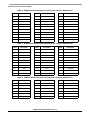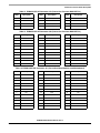
1
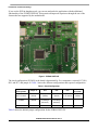
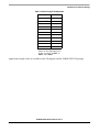
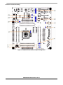
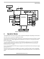
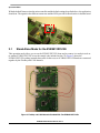
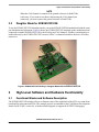
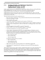
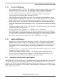
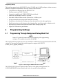
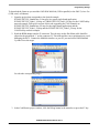
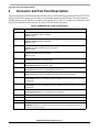
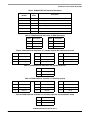
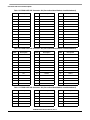
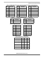
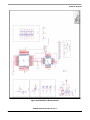
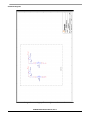
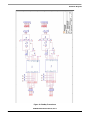
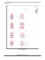
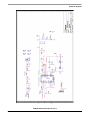
Freescale Semiconductor
User Manual
Document Number: EVB9S12XF512UM
Rev. 0, 06/2007
EVB9S12XF512E User Manual
by: Daniel Morfin
Guadalajara, Jal. Mexico
1
Introduction and Default
Settings
This kit contains everything you need to get started using
the EVB9S12XF512E, including a description of the pin
function of test points, jumpers, and connectors. This
document guides you through the steps necessary to
download your own program using a downloading tool
and connection. You can test the EVB9S12XF512E with
the sample code supplied on a data CD or with your own
application, which can be downloaded into the MCU.
This evaluation board (EVB) supports the M9S12XF512
in the 112 LQFP and 64 LQFP packages.
This EVB can work in two modes: stand alone and
daughter.
The stand-alone mode is used to program and test the
device assembled in the board. This allows you to create
and debug the application you want to use and to
integrate it into the system.
© Freescale Semiconductor, Inc., 2007. All rights reserved.
Contents
1
2
3
4
5
6
7
Introduction and Default Settings . . . . . . . . . . . . . . . . . . 1
Operation Modes . . . . . . . . . . . . . . . . . . . . . . . . . . . . . . . 5
2.1 Stand-Alone Mode for the EVB9S12XF512E . . . . . 6
2.2 Daughter Mode for EVB9S12XF512E . . . . . . . . . . . 7
High-Level Software and Hardware Functionality . . . . . . 7
3.1 Functional Blocks and Software Description . . . . . . 7
3.2 Hardware Functionality Description. . . . . . . . . . . . 11
Programming Settings . . . . . . . . . . . . . . . . . . . . . . . . . . 12
4.1 Programming Through Background
Debug Mode Tool . . . . . . . . . . . . . . . . . . . . . . . . . 12
Connector and Test Point Description. . . . . . . . . . . . . . 18
Schematic Diagrams . . . . . . . . . . . . . . . . . . . . . . . . . . . 24
Additional Information . . . . . . . . . . . . . . . . . . . . . . . . . . 30
7.1 Product Summary Pages. . . . . . . . . . . . . . . . . . . . 30
7.2 Datasheets . . . . . . . . . . . . . . . . . . . . . . . . . . . . . . 30
7.3 Tool Summary Pages . . . . . . . . . . . . . . . . . . . . . . 30
Introduction and Default Settings
If you use the EVB in daughter mode, you can run and probe the application with the additional
functionality of the EVB9S12XEP100. This permits an improved experience through the use of the
features that are supported by the motherboard.
Figure 1. EVB9S12XF512E
The clock configuration (XCLKS) in the board is determined by five components: resistors R17, R18,
R19, and R77, and jumper J6. Table 1 shows the different configurations and required configuration.
Table 1. Clock Configuration
Clock
Configuration
Jumper J6
R17
R18
Loop-controlled
Pierce oscillator
Position 2–3
(default)
Not populated
(default)
Populated 0 Ω
(default)
Populated
Not populated
2.2 K (default)
(default)
Full-swing Pierce
oscillator
Position 2–3
(default)
Populated
(according to
datasheet)
Populated
(according to
datasheet)
Not populated Populated 0 Ω
External clock
Position 1–2
Don’t care
Don’t care
R19
Don’t care
R77
Assembly
Populated 0 Ω
Table 2 shows the default jumper configuration for the EVB9S12XF512E.
EVB9S12XF512E User Manual, Rev. 0
2
Freescale Semiconductor
Introduction and Default Settings
Table 2. Default Jumper Configuration
Jumper
2–3
J5 MODC 1
1–2
J6 XTAL
2–3
J4 MODA
J7 MODB
1
Position
1
1
2–3
J9 SW2
Connected
J10 SW3
Connected
J26
Connected
J27 RESET
Connected
J30
Connected
J31
Connected
J32
Connected
Table 20 describes the modes the
S12XF can have depending on the
position of jumpers J4 MODA, J5
MODB, and J7 MODC.
Application example codes are available on the CD shipped with the EVB9S12XF512E package.
EVB9S12XF512E User Manual, Rev. 0
Freescale Semiconductor
3
Introduction and Default Settings
Figure 2. EVB9S12XF512E Default Jumper Configuration
EVB9S12XF512E User Manual, Rev. 0
4
Freescale Semiconductor
Operation Modes
Power supply
(J25/motherboard)
J32
SW4
SBC (+5 V
power supply)
D12
J26
SW1 reset
J27
SBC (CAN
transceiver)
J4 MOD A
J5 MOD C
Processing unit
S12XFR/S12SXF
J7 MOD B
J30
J31
BDM
connector
FlexRay
transceiver
FlexRay
transceiver
Crystal
Oscillator
J9
J6
Pushbuttons
LEDs
J10
8
4x28
Pins from
processing unit
4x36
Pins to
mother board
Figure 3. EVB9SXF512E Block Diagram
2
Operation Modes
The EVB9S12XF512E can be used in two modes: stand alone and daughter. Depending on which mode is
used, there are two ways power is supplied to the board.
In the stand-alone mode (default jumper configuration), slide switch SW4 must be in the STAND_ALONE
position and a 12 VDC voltage supply must be connected to J25, which is a 2.1 mm power jack with a
positive-center polarity.
To use the EVBMC9S12XF512E with the EVB9S12XEP100 motherboard, select the DAUGHTER
position in slide switch SW4 and disconnect jumper J26. The EVB9S12XF512E is powered by the
motherboard with a 5 V supply.
For powering the EVB9S12XF512E, the power supply from the motherboard or the external power supply
must not exceed 12 V.
If the EVB is going to be used as a daughter card, connect it carefully but firmly on the corresponding
connectors of the motherboard. Use the configuration and programming procedures of the motherboard
guide.
EVB9S12XF512E User Manual, Rev. 0
Freescale Semiconductor
5
Operation Modes
With the default firmware into the microcontroller and the default settings described above, the application
should run. The signals in the different connectors and the LEDs provide feedback on the evaluation board.
Figure 4. Stand Alone/Daughter Mode Switch
2.1
Stand-Alone Mode for the EVB9S12XF512E
This operation mode allows you to use the EVB9S12XF512E alone and to connect it to analysis tools or
to another EVB9S12XF512E to test the sample code included on the CD. Figure 5 shows the
EVB9S12XF512E working in stand-alone mode. In this case, two EVB9S12XF512E boards are connected
together by the FlexRay and CAN channels.
Figure 5. FlexRay and CAN Networks Enabled With Two EVB9S12XF512Es
EVB9S12XF512E User Manual, Rev. 0
6
Freescale Semiconductor
High-Level Software and Hardware Functionality
NOTE
When the CAN channel is connected, the ground reference for both EVBs
is the same. If you want to test them without using the CAN channel (not
connected), you must connect the ground reference of both EVBs.
2.2
Daughter Mode for EVB9S12XF512E
To use the EVB9S12XF512E in daughter mode, you need a EVB9S12XEP100 motherboard with the same
pin distribution and placement. Figure 6 shows one EVB9S12XF512E mounted on the motherboard and
connected to another EVB9S12XF512E by the FlexRay and CAN channels. FlexRay communication is
enabled directly by the EVB9S12XF512E, because SofTec’s evaluation board does not have a FlexRay
transceiver.
Figure 6. EVB9S12XF512E Working in Daughter Mode with the EVB9S12XEP100
3
High-Level Software and Hardware Functionality
3.1
Functional Blocks and Software Description
The EVB9S12XF512E includes software to illustrate some of the capabilities of the EVB, as a stand-alone
board and for interconnected EVBs. The example projects are intended for the CodeWarrior Development
Studio for HCS12(X) version 4.6, with the included upgrade to support the S12XF512 debugging.
EVB9S12XF512E User Manual, Rev. 0
Freescale Semiconductor
7
High-Level Software and Hardware Functionality
3.1.1
Low-Speed Stand-Alone Application
(EVB9S12XF512E_StandAlone_LS.mcp)
In this project, the EVB9S12XF512E is configured to operate as an isolated board. Its local
communication modules and the input/output capabilities are exercised to allow basic tests of the EVB
hardware integrity and verify the code downloading procedure.
The main functions performed in this example project are:
• Real-time interrupt configured to 500 ms period and used as the base time for the task scheduler
• SPI master operating at 500 kHz
• System basis chip (SBC) initialized in debug mode
• FlexRay module configured for wake-up frames transmission at 1.25 Mbit/s
• IRQ detection when SW2 is pressed, interrupt service indicated by toggling D26
• Input capture IOC7 stimulated by SW3, interrupt serviced by the XGATE and indicated by
toggling D24
• Microcontroller successive tasks are separated by 1 s intervals, the general-purpose LEDs are
activated by columns to indicate the task executed in this sequence:
— LEDs D22, D27, and D29
— LEDs D23, D25, and D28 (FlexRay wake-up frames transmission)
— LEDs D24 and D26
3.1.2
Low-Speed FlexRay Network Application
(EVB9S12XF512E_Node1_LS.mcp/
EVB9S12XF512E_Node2_LS.mcp)
This example requires two EVB9S12XF512E boards because each acts as a FlexRay node, exchanging
frames in a simple network. One EVB must be programmed using the EVB9S12XF512E_Node1_LS.mcp
project and the other must be programmed with the EVB9S12XF512E_Node2_LS.mcp code. Also,
FlexRay channels must be properly connected between the EVBs.
The main functions performed in this example project are:
• Real-time interrupt configured to 500 ms period and used as the base time for the task scheduler
• SPI master operating at 500 kHz
• SBC initialized in debug mode
• FlexRay module fully configured for frames transmission and reception at 1.25 Mbit/s; in Node1
the FlexRay events are interrupt driven, but in Node2 there is a polling procedure for the frames
handling
• LED indicators D22, D27, and D29 are sequentially turned on at 1 s intervals.
• FlexRay activity and frames interchange is indicated by the fast toggling of LEDs D23, D25, and
D28 at 1 s intervals; to ease visual perception, these LEDs are turned on each time the RTI is
serviced and turned off when a FlexRay function is performed.
For Node1, the LED activation is:
EVB9S12XF512E User Manual, Rev. 0
8
Freescale Semiconductor
High-Level Software and Hardware Functionality
•
•
3.1.3
— Slot 1 transmission, D23
— Slot 4 reception, D25
— Slot 62 reception, D28
For Node2, the LED activation is:
— Slot 1 reception, D23
— Slot 4 transmission, D25
— Slot 62 transmission, D28
IRQ detection when SW2 is pressed, interrupt service indicated by toggling D26
Input capture IOC7 stimulated by SW3, interrupt serviced by the XGATE and indicated by
toggling D24
Full-Speed Stand-Alone Application
(EVB9S12XF512E_StandAlone_FS.mcp)
In this example project the EVB9S12XF512E is configured to operate as an isolated board. Its local
communication modules and the input/output capabilities are exercised to allow basic tests of the EVB
hardware integrity and to verify the code downloading procedure.
The main functions performed in this example project are:
•
•
•
•
•
•
•
•
•
Real-time interrupt configured to 75 ms period and used as the base time for the task scheduler
SPI master operating at 2.5 MHz
SBC initialized in debug mode
CAN module configured for internal loopback transmission and reception at 500 kbit/s rate
FlexRay module configured for wake-up frames transmission
Periodic XGATE access to SBC through SPI channel, 75 ms period
Microcontroller successive tasks are separated by 225 ms intervals for a total period of 900 ms, the
general-purpose LEDs are activated by columns to indicate the task executed in the following
sequence:
— CAN internal loopback transmission/ reception, LED indicators D22, D27 and D29
— FlexRay wake-up frames transmission, LED indicators activated D23, D25 and D28
— D24 and D26 toggled
— LED indicators off
IRQ detection when SW2 is pressed, interrupt service indicated by toggling D26
Input capture IOC7 stimulated by SW3, interrupt serviced by the XGATE and indicated by
toggling D24
EVB9S12XF512E User Manual, Rev. 0
Freescale Semiconductor
9
High-Level Software and Hardware Functionality
3.1.4
Full-Speed FlexRay and CAN Network Application
(EVB9S12XF512E_Node1_FS.mcp/
EVB9S12XF512E_Node2_FS.mcp)
In this example you must use two EVB9S12XF512Es, because each one will act as a CAN and FlexRay
node exchanging frames in a simple network. One EVB must be programmed using the
EVB9S12XF512E_Node1_FS.mcp project. The other must be programmed with the
EVB9S12XF512E_Node2_FS.mcp code (this files are in the EVB9S12XF512E_Node1_FS.zip and
EVB9S12XF512E_Node2_FS.zip files, respectively). The CAN and FlexRay channels must be properly
connected between the EVBs.
The main functions performed in this example project are:
• Real-time interrupt configured to 75 ms period and used as the base time for the task scheduler
• SPI master operating at 2.5 MHz
• SBC initialized in debug mode
• CAN module configured for transmission and reception at 500 kbit/s rate
• FlexRay module fully configured for frames transmission and reception at 10 Mbit/s; in Node1 the
FlexRay events are interrupt driven, whereas in Node2 there is a polling procedure for the frames
handling
• LED D22 toggled each time the RTI is serviced (75 ms period)
• Periodic XGATE access to SBC through SPI channel (75 ms period)
• CAN frames transmission every 150 ms, LED D27 activated
• CAN reception is interrupt based, LED D29 is activated to indicate a CAN frame received
• FlexRay activity is indicated by the fast toggling of LEDs D23, D25, and D28; to ease visual
perception, these LEDs are turned on each time the RTI is serviced and turned off when a FlexRay
function is performed; for Node1 the LED activation is as follows:
— Slot 1 transmission, D23
— Slot 4 reception, D25
— Slot 62 reception, D28
For Node2 the LED activation is as follows:
— Slot 1 reception, D23
— Slot 4 transmission, D25
— Slot 62 transmission, D28
• IRQ detection when SW2 is pressed, interrupt service indicated by toggling D26
• Input capture IOC7 stimulated by SW3, interrupt serviced by the XGATE and indicated by
toggling D24
The described example projects consist of software modules divided into low-level basic subroutines near
the peripheral’s operation and handling of input/output lines, and high-level modules that define the
functional behavior of the EVB. The example software modules and the related files are described in the
next sections. Complementary software documentation can be accessed through the file index.html in the
subfolder \Doxygen\html in each example project folder.
EVB9S12XF512E User Manual, Rev. 0
10
Freescale Semiconductor
High-Level Software and Hardware Functionality
3.1.5
•
•
•
•
•
•
3.1.6
•
•
•
3.2
Low-Level Modules
Initial configuration (CPU.c, CPU.h)—This module has defined the initial conditions for the S12X
operation: bus clock PLL driven, IPLL for the FlexRay module, peripherals configuration,
interrupt settings for the real-time interrupt, PE0/XIRQ, and input capture on PT7/IOC7.
XGATE configuration and interrupts handling (xgate.cxgate, xgate.h)—The peripheral
co-processor services the input capture interrupt at PT7/IOC7.
General-purpose input output (GPIO_macros.h)—The output tasks are implemented as macros
that allow simple port handling. These macros are used to display output patterns to the general
purpose LEDs in the EVB to indicate the current operation mode and the occurrence of events.
SPI driver (SPI_driver.c, SPI_driver.h)—This module contains basic serial peripheral interface
subroutines, configuration of the SPI module as a master , and read and write functions for handling
the SBC.
System basis chip driver (SBC_driver.c, SBC_driver.h)—This module contains a set of functions
to configure the SBC CAN transceiver.
FlexRay unified driver (Fr_UNIFIED.c, Fr_UNIFIED_cfg.c, Fr_UNIFIED.h,
Fr_UNIFIED_cfg.h, Fr_UNIFIED_types.h)—The driver contains a set of functions in charge of
the FlexRay channel’s configuration, transmission, and reception of FlexRay messages. For proper
use of the driver and information regarding the node’s configuration, refer to the documentation
and example programs generated when the FlexRay UNIFIED driver is installed.
High-Level Modules
Interrupt service routines (Interrupts.c, Interrupts.h, Vectors.h)—Transitions generated through
pushbuttons SW2 and SW3, connected to PE0/XIRQ and PT7/IOC7 inputs, are individually
detected as interrupts and its occurrence is indicated by toggling LEDs D24 or D26. This module
also contains the service routines related to the scheduler and handling of CAN and FlexRay
interrupts.
Scheduler (Scheduler.c)—This module is called by the S12XF real-time interrupt service routine.
It assigns time frames for LEDs activation.
FlexRay frames handler (FlexRay_handler.c)—The FlexRay module configuration and the
functions related to timing and frames exchange are contained in this module, following an
interrupt-based scheme for Node1 and a poll-driven approach in Node2.
Hardware Functionality Description
The EVB9S12XF512E has support for one CAN channel and two FlexRay channels (for 112 pin package
only; the 64 pin package has one FlexRay channel). For the CAN channel the inputs can be seen on
connectors TP7 (CANL) and TP8 (CANH). The inputs of the FlexRay Channel A are on connector J11
and the outputs are on connector J12.The FlexRay Channel B inputs are on connector J14 and the output
can be seen on connector J15.
EVB9S12XF512E User Manual, Rev. 0
Freescale Semiconductor
11
Programming Settings
The board has support for the M9S12XF512 in the 112 LQFP and 64 LQFP packages, with no necessary
hardware configuration adjustments. The major features of the board are:
• CAN transceiver integrated into the SBC MC33742
• FlexRay transceivers (NXP TJA1080)
• Connection capability with EVB9S12XEP100 motherboard.
• Stand-alone and daughter modes of operation.
• Selectable 4 MHz oscillator module (socketed) or a 4 MHz crystal.
• All microcontroller pins mirrored on connectors for testing.
• Possibility to disconnect the FlexRay ports from the transceivers for other applications.
• Double protection to avoid shortages when changing from stand-alone mode to daughter mode.
• Reset inputs for both the microcontroller and the SBC (through jumper J27).
• Eight user LEDs and two push buttons
4
Programming Settings
4.1
Programming Through Background Debug Mode Tool
NOTE
Jumper J27 must be disconnected before programming. After programming,
reconnect J27 to enable the reset line for the SBC.
The steps described to program the device are intended for CodeWarrior Development Studio for HC12X,
version 4.6. You must also install the included upgrade to support the S12XF512
(CW46_XF512_upgrade_beta0.zip).
Debug Interface
USB
EVB9s12XF512E
BDM Multilink or Multilink Cyclone Pro
Figure 7. Connecting the EB9S12XF512E to a Host
The EVB9S12XF512E has pre-flashed code for the low-seed stand-alone application. The
S12XFSTARTERKITE has pre-flashed code for the low-speed FlexRay application.
EVB9S12XF512E User Manual, Rev. 0
12
Freescale Semiconductor
Programming Settings
To download the firmware you need the P&E BDM Multilink (USB or parallel) or the P&E Cyclone Pro
(USB, serial, or Ethernet).
1. Open the project that corresponds to the desired example:
EVB9S12XF512E_StandAlone_LS.mcp for low-speed single board application,
EVB9S12XF512E_Node1_LS.mcp or EVB9S12XF512E_Node2_LS.mcp for the CAN/FlexRay
network example. Full-speed versions of this code supporting the CAN channels are
EVB9S12XF512E_StandAlone_FS.mcp for the single-board applications and the
EVB9S12XF512E_Node1_FS.mcp and the EVB9S12XF512E_Node2_FS.mcp for the
CAN/FlexRay network example.
2. Hook the BDM adapter into the J2 connector. The red stripe on the flat ribbon cable should be
aligned to the pin marked ‘1’ on the connector J2. This indicated the correct polarization to avoid
damaging the MCU. Connect the Multilink interface to your PC port and select P&E Multilink
Cyclone Pro as the target.
Or select the corresponding target:
3. In the CodeWarrior project window, click the Debug button in the menu bar or press the F5 key.
EVB9S12XF512E User Manual, Rev. 0
Freescale Semiconductor
13
Programming Settings
4. If the board is powered and the BDM connections is correct, the True-Time Simulator & Real-Time
Debugger application starts and this window appears:
5. Next, this warning message window appears:
6. Click OK. A final window appears, showing the progress of the device programming.
7. After the flash programming process finishes, unplug the BDM connector and reconnect J27.
If an error occurs during the process, one of the following windows could appear:
EVB9S12XF512E User Manual, Rev. 0
14
Freescale Semiconductor
Programming Settings
8. To correct the issue, confirm that the correct device is selected within the True-Time Simulator &
Real-Time Debugger:
9. Select the proper device from the pull-down list:
10. If the MC9S12XF512 is not shown, run the CW46_XF512_upgrade_beta0.zip upgrade.
EVB9S12XF512E User Manual, Rev. 0
Freescale Semiconductor
15
Programming Settings
11. Next, set the connection speed by choosing Set Communication Speed from the Multilink Cyclone
Pro menu.
12. The following window appears. Enter the clock divider value and check the Auto detect option or
use the equations shown to calculate the divider depending on the connection method (the
oscillator frequency for the M9S12XF512 is 4 MHz):
13. The clock interface configuration is verified and, if necessary, the selected processor and
connection method should be fixed:
EVB9S12XF512E User Manual, Rev. 0
16
Freescale Semiconductor
Programming Settings
Use the parameters shown :
14. Click OK. The connection is re-attempted automatically. The physical channel for the connection
can be modified if the problem persists. Select MultiLinkCyclonePro from the menu bar and
choose Communication to open the communication settings in the application:
15. Choose the corresponding communication port and press the OK. The connection is attempted one
more time.
EVB9S12XF512E User Manual, Rev. 0
Freescale Semiconductor
17
Connector and Test Point Description
5
Connector and Test Point Description
This section describes the function of the different jumpers and switches present in the EVB9S12XF512E.
It also describes the signals on each of the test points and connectors of the board. The input signals to
FlexRay transceivers A and B are available via test points of J11 and J14. A single-row connector of nine
pins can be assembled to the board in J11 and J14 for pin header test points.
Table 3. EVB9SI2XF512E Jumpers and Switches
Jumper name
Functional Description
J4
Position 1–2: MODA in MCU is enabled.
Position 2–3: MODA in MCU is disabled.
Other: Not valid
J5
Position 1–2: MODB in MCU is enabled.
Position 2–3: MODB in MCU is disabled.
Other: Not valid
J6
Position 1–2: Oscillator drives MCU.
Position 2–3: 4 MHz or 40 MHz crystal drives MCU.
Other: Not valid
J7
Position 1–2: MODC in MCU is enabled.
Position 2–3: MODC in MCU is disabled.
Other: Not valid
J9
Connected: Enables push button SW2.
Not connected: Disables push button SW2.
J10
Connected: Enables push button SW3.
Not connected: Disables push button SW3.
J26
Connected: Power to the board will be supplied by the 5 V supply of the SBC.
Not connected: Power will be supplied by the motherboard.
J27
Connected: Connects the *RESET signal to the reset pin of U4 (SBC).
Not connected: Disconnects the *RESET signal from the reset pin of U4 (SBC).
J30
Connected: The pins from FlexRay Channel A are connected to U2 (FlexRay transceiver A).
Not connected: The pins from FlexRay Channel A of MCU are disconnected from U2 (FlexRay
transceiver A).
J31
Connected: The pins from FlexRay Channel B are connected to U3 (FlexRay transceiver B).
Not connected: The pins from FlexRay Channel B of MCU are disconnected from U3 (FlexRay
transceiver B).
J32
Connected: Enables the use of D12 (power-on indicator).
Not connected: Disables the use of D12 (power-on indicator).
SW1
Reset signal to the MCU and/or SBC (connected to SBC through J27).
SW2
Test pushbutton.
SW3
Test pushbutton.
SW4
STAND_ALONE: Enables the evaluation board to be used as a stand-alone device.
DAUGHTER: Enables the evaluation board to draw power from the motherboard when it is
connected as a daughter board.
EVB9S12XF512E User Manual, Rev. 0
18
Freescale Semiconductor
Connector and Test Point Description
Table 4. EVB9S12XF512E Test Point Description
Test Point
Number
Signal
Name
TP1, TP2, TP6
GND
TP3
RX
Receive signal of SCI module (PS0)
TP4
TX
Transmit signal of SCI module (PS1)
TP5
+5V
5 V power supply output
TP7
CANL
Low line of the SBC’s CAN transceiver
TP8
CANH
High line of the SBC’s CAN transceiver
Description
System ground, electrical reference test point
Table 5. EVB9S12XF512E Connector J2 (BDM Connector)
PIN#
Description
PIN#
Description
1
BKGD
4
RESET
2
GND
5
NC
3
NC
6
VDD
Table 6. EVB9S12XF512E Connector J11 (FlexRay Input A) Not assembled in board
PIN#
Description
PIN#
Description
PIN#
Description
1
RXEN_A
4
STBN_A
7
TXEN_A
2
ERRN_A
5
BGE_A
8
TXD_A
3
Wake_A
6
RXD_A
9
EN_A
Table 7. EVB9S12XF512E Connector J12 (FlexRay Output A)
PIN#
Description
1
BP_A
2
BM_A
Table 8. EVB9S12XF512E connector J14 (FlexRay Input B)
PIN#
Description
PIN#
Description
PIN#
Description
1
RXEN_B
4
STBN_B
7
TXEN_B
2
ERRN_B
5
BGE_B
8
TXD_B
3
Wake_B
6
RXD_B
9
EN_B
Table 9. EVB9S12XF512E connector J15 (FlexRay output B) not assembled in board
PIN#
Description
1
BP_B
2
BM_B
EVB9S12XF512E User Manual, Rev. 0
Freescale Semiconductor
19
Connector and Test Point Description
Table 10. EVB9S12XF512E Connector J17 (One-to-One Pins from M9S12XF512)
PIN#
Description
PIN#
Description
PIN#
Description
1
PP1
11
PJ0
20
PT6
2
PP0
12
PJ1
21
PT7
3
PD3
13
PJ2
22
PJ3
4
PD2
14
VDDF
23
PJ4
5
PD1
15
VSS1
24
PJ5
6
PD0
16
VSSX3
25
PJ6
7
PT0
17
VDDX3
26
PJ7
8
PT1
18
PT4
27
PB0
9
PT2
19
PT5
28
PB1
10
PT3
Table 11. EVB9S12XF512E Connector J18 (One-to-One Pins from M9S12XF512)
PIN#
Description
PIN#
Description
PIN#
Description
1
BKGD
11
PH7
20
EXTAL
2
PE7
12
VDDX2
21
XTAL
3
PE6
13
VSSX2
22
TEST
4
PE5
14
VSS3
23
PA0
5
PE4
15
VDDR
24
PA1
6
PE3
16
RESET*
25
PA2
7
PE2
17
VDDPLL
26
PA3
8
PH4
18
XFC
27
*IRQ/PE1
9
PH5
19
VSSPLL
28
PE0
10
PH6
Table 12. EVB9S12XF512E Connector J19 (One-to-One Pins from M9S12XF512)
PIN#
Description
PIN#
Description
PIN#
Description
1
PH0
11
PAD00
20
PAD12
2
PH1
12
PAD08
21
PAD05
3
PH2
13
PAD01
22
PAD13
4
PH3
14
PAD09
23
PAD06
5
PA4
15
PAD02
24
PAD14
6
PA5
16
PAD10
25
PAD07
EVB9S12XF512E User Manual, Rev. 0
20
Freescale Semiconductor
Connector and Test Point Description
Table 12. EVB9S12XF512E Connector J19 (One-to-One Pins from M9S12XF512)
PIN#
Description
PIN#
Description
PIN#
Description
7
PA6
17
PAD03
26
PAD15
8
PA7
18
PAD11
27
VDDA
9
VDD2
19
PAD04
28
VRH
10
VSS2
Table 13. EVB9S12XF512E Connector J20 (One-to-One Pins from M9S12XF512)
PIN#
Description
PIN#
Description
PIN#
Description
1
VRL
11
PM7
20
VDDX1
2
VSSA
12
PM6
21
PD5
3
PS0
13
PM5
22
PD4
4
PS1
14
PM4
23
PP7
5
PS2
15
PM3
24
PP6
6
PS3
16
PM2
25
PP5
7
PS4
17
PM1
26
PP4
8
PS5
18
PM0
27
PP3
9
PS6
19
VSSX1
28
PP2
10
PS7
Table 14. EVB9S12XF512E Connector J21 (One-to-One Name/Sockets from Motherboard)
PIN#
Description
PIN#
Description
PIN#
Description
1
PM7
13
PT2
25
BKGD
2
PM6
14
PT3
26
VDDX2
3
PM5
15
VDDF
27
VSSX2
4
PM4
16
VSS1
28
NC
5
NC
17
PT4
29
NC
6
NC
18
PT5
30
NC
7
NC
19
PT6
31
NC
8
NC
20
PT7
32
PB0
9
NC
21
NC
33
PB1
10
NC
22
NC
34
NC
11
PT0
23
NC
35
NC
12
PT1
24
NC
36
PP0
EVB9S12XF512E User Manual, Rev. 0
Freescale Semiconductor
21
Connector and Test Point Description
Table 15. EVB9S12XF512E Connector J22 (One-to-One Name/Sockets from Motherboard)
PIN#
Description
PIN#
Description
PIN#
Description
1
PP1
13
PE6
25
NC
2
PP2
14
PE5
26
NC
3
PP3
15
PE4
27
NC
4
NC
16
VSSX2
28
NC
5
NC
17
VDDX2
29
PD0
6
NC
18
*RESET
30
PD1
7
NC
19
VDDPLL
31
PD2
8
NC
20
NC
32
PD3
9
NC
21
VSSPLL
33
PE3
10
NC
22
NC
34
PE2
11
NC
23
NC
35
*IRQ/PE1
12
PE7
24
VSSPLL
36
PE0
Table 16. EVB9S12XF512E Connector J23 (One-to-One Name/Sockets from Motherboard)
PIN#
Description
PIN#
Description
PIN#
Description
1
PA0
13
NC
25
PAD04
2
PA1
14
NC
26
PAD12
3
PA2
15
VDD2
27
PAD05
4
PA3
16
VSS2
28
PAD13
5
PA4
17
PAD00
29
PAD06
6
PA5
18
PAD08
30
PAD14
7
PA6
19
PAD01
31
PAD07
8
PA7
20
PAD09
32
PAD15
9
VSS3
21
PAD02
33
NC
10
VDDX3
22
PAD10
34
NC
11
PD4
23
PAD03
35
VDDA
12
PD5
24
PAD11
36
VRH
Table 17. EVB9S12XF512E Connector J24 (One-to-One Name/Sockets from Motherboard)
PIN#
Description
PIN#
Description
PIN#
Description
1
VRL
13
PS2
25
NC
2
VSSA
14
PS3
26
NC
3
NC
15
PS4
27
NC
4
NC
16
PS5
28
PM1
5
NC
17
PS6
29
PM0
EVB9S12XF512E User Manual, Rev. 0
22
Freescale Semiconductor
Connector and Test Point Description
Table 17. EVB9S12XF512E Connector J24 (One-to-One Name/Sockets from Motherboard)
PIN#
Description
PIN#
Description
PIN#
Description
6
NC
18
PS7
30
VSSX1
7
NC
19
NC
31
VDDX1
8
NC
20
NC
32
NC
9
NC
21
NC
33
PP7
10
NC
22
NC
34
PP6
11
PS0
23
NC
35
PP5
12
PS1
24
NC
36
PP4
Table 18. EVB9S12XF512E Connector J29 (HSCAN Connector)
PIN#
Description
PIN#
Description
1
CANH Bus_SBC
3
GND
2
CANL Bus_SBC
4
NC
Table 19. EVB9S12XF512E Connector J33 (DIP 14 Socket for Oscillator)
PIN#
Description
PIN#
Description
1
GND
8
OSC OUT
2
NC
9
NC
3
NC
10
NC
4
GND
11
OSC OUT
5
NC
12
NC
6
NC
13
NC
7
GND
14
VDD
Table 20. Chip Modes for M9S12XF512
Chip Modes
MODC
MODB
MODA
Normal single chip
1
0
0
Special single chip
0
0
0
Emulation single chip
0
0
1
Normal expanded
1
0
1
Emulation expanded
0
1
1
Special test
0
1
0
EVB9S12XF512E User Manual, Rev. 0
Freescale Semiconductor
23
Schematic Diagrams
NOTE
These operation modes for the M9S12XF512 are entered by using jumpers
J4 MODA, J5 MODB, and J7 MODC.
6
Schematic Diagrams
Figure 8 through Figure 12 in this section show the schematic diagram of the EVB9S12XF512E.
EVB9S12XF512E User Manual, Rev. 0
24
Freescale Semiconductor
Schematic Diagrams
Figure 8. MC9S12XF512 Microcontroller
EVB9S12XF512E User Manual, Rev. 0
Freescale Semiconductor
25
Schematic Diagrams
Figure 9. Power Supply Conditioning and Push Buttons
EVB9S12XF512E User Manual, Rev. 0
26
Freescale Semiconductor
Schematic Diagrams
Figure 10. FlexRay Transceivers
EVB9S12XF512E User Manual, Rev. 0
Freescale Semiconductor
27
Schematic Diagrams
Figure 11. Signal Pins
EVB9S12XF512E User Manual, Rev. 0
28
Freescale Semiconductor
Schematic Diagrams
Figure 12. Power Supply
EVB9S12XF512E User Manual, Rev. 0
Freescale Semiconductor
29
Additional Information
7
Additional Information
This section contains links to the product summary pages, data sheets, and other useful information for the
EVB9S12XF512E.
7.1
•
•
7.2
•
•
•
7.3
•
•
•
•
Product Summary Pages
Freescale M9S12XF512:
http://www.freescale.com/webapp/sps/site/prod_summary.jsp?code=MC9S12XF512
Freescale MC33742:
http://www.freescale.com/webapp/sps/site/prod_summary.jsp?code=MC33742
Datasheets
Freescale MC9S12XF512 Reference Manual:
http://www.freescale.com/files/microcontrollers/doc/ref_manual/MC9S12XF512V1RM.pdf
Freescale MC33742: http://www.freescale.com/files/analog/doc/data_sheet/MC33742.pdf
NXP Homepage: http://www.nxp.com/
Tool Summary Pages
Freescale S12XF Starter Kit (S12XFSTARTERKITE)
http://www.freescale.com/webapp/sps/site/prod_summary.jsp?code=S12XFSTARTERKITE
Freescale S12XF Evaluation Board (EVB9S12XF512E)
http://www.freescale.com/webapp/sps/site/prod_summary.jsp?code=EVB9S12XF512E
EVB9S12XF512E User Manual, Rev. 0
30
Freescale Semiconductor
THIS PAGE IS INTENTIONALLY BLANK
EVB9S12XF512E User Manual, Rev. 0
Freescale Semiconductor
31
How to Reach Us:
Home Page:
www.freescale.com
Web Support:
http://www.freescale.com/support
USA/Europe or Locations Not Listed:
Freescale Semiconductor, Inc.
Technical Information Center, EL516
2100 East Elliot Road
Tempe, Arizona 85284
+1-800-521-6274 or +1-480-768-2130
www.freescale.com/support
Europe, Middle East, and Africa:
Freescale Halbleiter Deutschland GmbH
Technical Information Center
Schatzbogen 7
81829 Muenchen, Germany
+44 1296 380 456 (English)
+46 8 52200080 (English)
+49 89 92103 559 (German)
+33 1 69 35 48 48 (French)
www.freescale.com/support
Japan:
Freescale Semiconductor Japan Ltd.
Headquarters
ARCO Tower 15F
1-8-1, Shimo-Meguro, Meguro-ku,
Tokyo 153-0064
Japan
0120 191014 or +81 3 5437 9125
[email protected]
Asia/Pacific:
Freescale Semiconductor Hong Kong Ltd.
Technical Information Center
2 Dai King Street
Tai Po Industrial Estate
Tai Po, N.T., Hong Kong
+800 2666 8080
[email protected]
For Literature Requests Only:
Freescale Semiconductor Literature Distribution Center
P.O. Box 5405
Denver, Colorado 80217
1-800-441-2447 or 303-675-2140
Fax: 303-675-2150
[email protected]
Document Number: EVB9S12XF512UM
Rev. 0
06/2007
Information in this document is provided solely to enable system and software
implementers to use Freescale Semiconductor products. There are no express or
implied copyright licenses granted hereunder to design or fabricate any integrated
circuits or integrated circuits based on the information in this document.
Freescale Semiconductor reserves the right to make changes without further notice to
any products herein. Freescale Semiconductor makes no warranty, representation or
guarantee regarding the suitability of its products for any particular purpose, nor does
Freescale Semiconductor assume any liability arising out of the application or use of any
product or circuit, and specifically disclaims any and all liability, including without
limitation consequential or incidental damages. “Typical” parameters that may be
provided in Freescale Semiconductor data sheets and/or specifications can and do vary
in different applications and actual performance may vary over time. All operating
parameters, including “Typicals”, must be validated for each customer application by
customer’s technical experts. Freescale Semiconductor does not convey any license
under its patent rights nor the rights of others. Freescale Semiconductor products are
not designed, intended, or authorized for use as components in systems intended for
surgical implant into the body, or other applications intended to support or sustain life,
or for any other application in which the failure of the Freescale Semiconductor product
could create a situation where personal injury or death may occur. Should Buyer
purchase or use Freescale Semiconductor products for any such unintended or
unauthorized application, Buyer shall indemnify and hold Freescale Semiconductor and
its officers, employees, subsidiaries, affiliates, and distributors harmless against all
claims, costs, damages, and expenses, and reasonable attorney fees arising out of,
directly or indirectly, any claim of personal injury or death associated with such
unintended or unauthorized use, even if such claim alleges that Freescale
Semiconductor was negligent regarding the design or manufacture of the part.
RoHS-compliant and/or Pb-free versions of Freescale products have the functionality
and electrical characteristics as their non-RoHS-compliant and/or non-Pb-free
counterparts. For further information, see http://www.freescale.com or contact your
Freescale sales representative.
For information on Freescale’s Environmental Products program, go to
http://www.freescale.com/epp.
Freescale™ and the Freescale logo are trademarks of Freescale Semiconductor, Inc.
All other product or service names are the property of their respective owners.
© Freescale Semiconductor, Inc. 2007. All rights reserved.