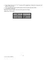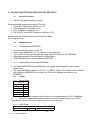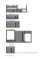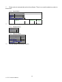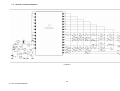
1
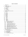
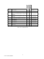
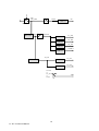
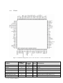
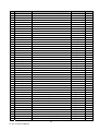
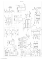
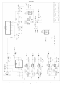
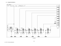
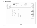
20” TFT TV
SERVICE MANUAL
(17MB18)
TABLE OF CONTENTS
1.
INTRODUCTION ...................................................................................................................................3
Scope .................................................................................................................................................3
General Features ...............................................................................................................................3
2.
SYSTEM BUILDING BLOCKS ..............................................................................................................4
2.1. Analog Front End ...............................................................................................................................4
2.1.1. Tuner...........................................................................................................................................4
2.1.2. SAW Filters .................................................................................................................................5
2.2. Back End............................................................................................................................................5
2.3. Side Board(s) .....................................................................................................................................8
2.3.1. Keypads ......................................................................................................................................8
2.3.2. IR&Led Board .............................................................................................................................8
2.4. Power .................................................................................................................................................8
3.
IC AND COMPONENT DESCRIPTIONS ............................................................................................11
3.1. Basic IC List .....................................................................................................................................11
3.2. UOCIII ..............................................................................................................................................11
3.2.1. Pinout........................................................................................................................................12
3.3. PW1306 ...........................................................................................................................................16
3.3.1. Pinout........................................................................................................................................16
3.4. M29W800AT ....................................................................................................................................25
3.5. DS90C385........................................................................................................................................25
3.6. P15V330 ..........................................................................................................................................25
3.7. 74HC4052 ........................................................................................................................................25
3.8. TA1366FG........................................................................................................................................26
3.9. TDA7056A........................................................................................................................................26
3.10.
TDA1308 ......................................................................................................................................26
3.11.
LM1117.........................................................................................................................................27
3.12.
24LC32 .........................................................................................................................................27
3.13.
24LC21 .........................................................................................................................................27
3.14.
74LVC541.....................................................................................................................................28
3.15.
SAA3010T ....................................................................................................................................28
3.16.
MC34167 ......................................................................................................................................29
3.17.
TFMS5360....................................................................................................................................29
3.18.
Board Connectors, Headers & Jumpers.......................................................................................29
3.18.1.
Analog PC Connector (PL400)..............................................................................................29
3.18.2.
Scart Connector (PL401) ......................................................................................................30
3.18.3.
S-Video Connector (JK403) ..................................................................................................30
3.18.4.
LVDS Panel Connector(1x20 PL179) ...................................................................................30
3.18.5.
TTL Panel Connector -Even (2x17 PL177)...........................................................................31
3.18.6.
TTL Panel Connector -Odd (2x17 PL178) ............................................................................31
3.18.7.
Panel Inverter Connector (1x11 PL176) ...............................................................................31
3.18.8.
Keypad Card Connector (1x5 PL175)...................................................................................32
3.18.9.
Optional Keypad Connector to UOC (1x2 PL 202) ...............................................................32
3.18.10. LED & IR Receiver Connector (1x6 PL202)..........................................................................32
3.18.11. Optional Rocker Sw. Connector (1x4 PL500) .......................................................................32
3.18.12. PROMJet Connector (2x25 PL101) ......................................................................................32
3.18.13. Side HP Connector for Side-card Option (PL405) ................................................................32
3.18.14. Side AV Connector for Side-card Option (PL406) ................................................................33
3.18.15. Side SVHS Connector for Side-card Option (PL407) ...........................................................33
4.
SERVICE MENU SETTINGS ..............................................................................................................34
4.1. UOCIII Service Menu .......................................................................................................................34
4.1.1. UOCIII Service Menu Settings..................................................................................................34
4.1.2. Tuner AGC Alignment...............................................................................................................38
4.1.3. DCXO Alignment.......................................................................................................................38
4.2. PW1306 Service Menu ....................................................................................................................38
4.2.1. UOC Horizontal Position...........................................................................................................39
4.2.2. UOC Calibration........................................................................................................................39
4.2.3. PW1306 PC Input ADC Calibration ..........................................................................................39
1.1.
1.2.
i
17” TFT TV Service Manual
19/11/2003
4.2.4. Init NVM ....................................................................................................................................40
4.2.5. Initial APS .................................................................................................................................40
4.2.6. Country .....................................................................................................................................40
4.2.7. Language ..................................................................................................................................40
4.2.8. Menu Background.....................................................................................................................40
4.2.9. Remote Control.........................................................................................................................40
4.3. Panel Type Change Shortcut...........................................................................................................40
5.
PRODUCTION SETTINGS AND FACTORY DEFAULTS...................................................................42
5.1. Production Schedule ........................................................................................................................42
5.2. EEPROM Settings............................................................................................................................42
5.2.1. Creating Master EEPROM........................................................................................................42
5.2.2. Creating Mass Production EEPROM........................................................................................42
5.3. TV Menu...........................................................................................................................................42
5.3.1. Picture Menu.............................................................................................................................42
5.3.2. Audio Menu...............................................................................................................................42
5.3.3. Window Menu ...........................................................................................................................43
5.3.4. Options Menu............................................................................................................................43
5.3.5. Settings Menu ...........................................................................................................................43
5.4. PC Mode Menu ................................................................................................................................43
5.4.1. Picture Menu.............................................................................................................................43
5.4.2. Audio Menü...............................................................................................................................44
5.4.3. Window Menu ...........................................................................................................................44
5.4.4. Options Menü............................................................................................................................44
6.
BLOCK DIAGRAM...............................................................................................................................45
7.
CIRCUIT DIAGRAMS ..........................................................................................................................47
7.1. 17MB18 Main Board Schematics.....................................................................................................47
7.2. Keypad Schematics .........................................................................................................................52
7.3. IR&LED Board Schematics..............................................................................................................53
7.4. Remote Controller Schematics ........................................................................................................54
ii
17” TFT TV Service Manual
19/11/2003
1.
INTRODUCTION
1.1. Scope
The document covers 20” (17MB18) chassis building blocks, basic features, service menu settings, and the other
information needed by service personal.
1.2. General Features
The system is a 14” to 20” TFT LCD TV solution with UOCIII Versatile Signal Processor and PW1306 Video Image
Processor chip-set on 4-layer PCB. The TV will support PAL/SECAM B/G/D/K/I/L/L’.
The other general default features of the TV are as listed below:
• 1 Full Scart input (with SVHS support)
• 1 SVHS input through standard S-Video interface.
• 1 CVBS input through standard RCA jack
• 75 ohms antenna input
• D-Sub 15 PC Input
• GERMAN + NICAM STEREO
• <3W S/B Power Consumption from mains supply
• 2x3W Speaker Output Power @16 Ohm spks; HP Output, Stereo Audio line out
• Stereo Audio line in
• Equalizer
• IR Control (RC5)
• OSD;Menu Languages ENG, FRA, GER, ITA, SPA, POR, TUR, SWE, DEN, FIN, NOR, POL, HUN, CZE, BUL,
ARA, PER, RUS (subject to change and be grouped)
• Teletext
• 2H/4H Comb Filter
• White balance settings (warm/normal/cool) for TV&PC
• Full AIR&CABLE band coverage
• Auto Shut down
2.
SYSTEM BUILDING BLOCKS
17MB18 chassis main blocks are as follows:
•
Analog Front End
: UOCIII (Microcontroller + Video Proccessor + Sound Proccessor + IF), CTI, Tuner, SAW
filters, Audio Amp., DAC
•
Back End
: PW1306(Microcontroller, Scaler, OSD, Keyboard/IR Interface)
•
Side Board(s)
: Keyboards, IR/LED Boards, TTL Panel Interface Cards, VCbCr Input Board (Optional)
2.1.
Analog Front End
17MB18 Main Board consists of two major blocks. The first block is analog front-end and this block is handled by
UOCIII chip that is highly multifunctional. This IC does demodulation of Video & Audio from Tuner IF, CVBS, Audio,
RGB, SVHS input selection and processing. It has an audio processor that supports equalizer or tone control, volume
control, AVL, surround effect etc and supplies amplifier, headphone and CVBS & audio line outputs. It handles video
processing such as colour standard detection and demodulation, picture alignment (brightness, contrast, colour etc.). The
IC also does teletext decoding with 10 pages text memory. After video processing, the processed video is applied to
PW1306 chip in RGB format.
The TV Tuner is an asymmetrical IF output type and is PLL controlled. For multistandard reception, a switchable SAW
filter is used as the sound filter and it is controlled by SAW_SW output from UOC. After the SAW filter block, IF signal
is applied to UOC IF inputs (VIFIN[1,2] and SIF[1,2]).
As UOCIII can handle all the audio processing, there is no need for additional audio processor solution on the board.
UOC supports three Audio outputs. These outputs are assigned to Headphone, Speaker and Scart Audio line outputs. The
board employs TDA7056A and TDA1308 to drive speaker and headphone outputs respectively. As another dedicated
output for Audio Line out from jack is not possible in UOC, this line out signal is obtained by using I2S input DAC
CS4335. UOCIII I2S output is converted to anolog signal by DAC CS4335.
2.1.1.Tuner
As the thickness of the TV set has a limit, a horizontal mounted tuner with longer connector is used in the
product. The tuning is available through the digitally controlled I2C bus (PLL). Below you will find info on the
Asymmetrical Tuner in use.
General description:
The tuner meets a wide range of applications. It is a combined VHF, UHF tuner suitable for CCIR systems
B/G, H, L, L’, I and I’. The low IF output impedance drives a wide variety of SAW filters with sufficient
suppression of triple transient.
Features:
• Small sized UHF/VHF tuners
• Systems CCIR: B/G, H, L, L’, I and I’; OIRT: D/K
• Digitally controlled (PLL) tuning via I2C-bus
• Off-air channels, S-cable channels and Hyper band
• ZS(AE) Aerial source impedance (unbalanced) 75 Ohm
PIN
1
2
3
4
5
6
7
8
9
SYMBOL
DESCRIPTION
AGC
TU
AS
SCL
SDA
n.c.
Automatic Gain Control Voltage 4 ±0.1
Tuning voltage monitor (output)
I 2C-Bus Address Select
I 2C-Bus Serial Clock
I 2C-Bus Serial Data
Not Connected
Vs
ADC
VST
Supply Voltage +5V ±0.125
ADC Input
Fixed tuning Supply Voltage +33V ±0.5
10
11
M1,M2,M3,
M4
I.F out 2
I.F out 1
Symmetrical I.F output 2 / Do not connect for asymmetrical
Asymmetrical I.F Output / Symmetrical I.F output 1
GND
Mounting Tags (Ground)
2.1.2.
SAW Filters
K3953M is an IF Filter for Video Applications. The package is SIP5K. Supported standards are B/G, D/K, I,
L/L’.
K9656M is an IF Filter for Audio Applications. The package is SIP5K. Supported standards are B/G, D/K, I,
L/L’.
2.2.
Back End
The Back End section is handled by PW1306 chip. This IC has built in ADC’s for RGB and SOY support. The RGB input
can handle standard interlaced RGB output from UOC, PC VGA RGB input. As only 1 set of ADC is present in PW1306
these sources should be multiplexed.
All the multiplexing operations are controlled by PW1306 via YUV_TV_SW (58) and VGA_TV_SW (57) signals.
A: VGA _TV_SW
B: YUV _TV_SW
A
B
SYNC SOURCE
0
0
UOC
0
1
VGA
1
0
YcbCr
1
1
NOT USED
Table 2: H/V Sync Multiplexing Table
The video output from PW1306 is a 48-bit digital RGB bus format and made available on two separate connectors with
TTL control signals (i.e. HS, VS, CLK, etc.). This digital output is intended to interface to TTL compatible display
devices. As PW1306 does not have integrated LVDS transmitter, 24 bit (even part of RGB) video output and TTL control
signals from PW1306 are also inputted to DS90C385 LVDS IC to produce single pixel LVDS output for LVDS
compatible LCDs.
Backlight control is also possible via PW1306 Porta7 pin (PWMOUT, PL176-10), that is a variable duty-cycle pulse
generator output.
5
17” TFT TV Service Manual
19/11/2003
MUX BLOCK
TV_[HS,VS]
PC_[HS,VS]
AHSYNC
AVSYNC
MUX
74HC4052D
HD_[HS,VS]
Control Signals:
VGA_TV_SW
YUV_TV_SW
YCbCr
[R,G,B]OUT
VIDEO
SWITCH
P15V330
TV_[R,G,B]AIN
VIDEO
SWITCH
P15V330
V[R,G,B]IN
RGB
Figure 1: MUX Block.
6
17” TFT TV Service Manual
19/11/2003
RF in
SAW
UOCIII
VFIN (24,25)
Y4(51)
C4(52)
CVBS3/Y3(58)
AUDIOIN5L(34)
AUDIOIN5R(35)
C2(59)
CVBS2/Y2(55)
IFVO(43)
AUDIOUTSL(36)
AUDIOUTSR(37)
S-Video in
CVBS in
Scart
AUDIOIN3L(56)
AUDIOIN3R(57)
TV_HS
TV_VS
Audio in
74HC14
VDRA,HOUT(23,67)
FBLIN
AUDOUTHP[L,R](62,63)
HP DRIVER
TDA1308
AUDOUTLS[L,R](60,61)
AUDIO
AMPLIFIER
2xTDA7056
FBLIN
R,G,B(78,79,80)
[R,G,B]IN
CTI/
LTI
SANDC
[Y,U,V]OUT(74,75,76)
YUV(72,71,70)
I2SDO2(104)
I2SCLK(103)
I2SWS(102)
YCbCr
Y
Audio
line out
[R,G,B]OUT(85,86,87)
HD_[HS,VS]
[R,G,B]OUT
MACROVISION
SYNC
SEPARATOR
EL1883
DAC
CS4335
MUX
BLOCK
Comunication
Signals:
I2C and Handhake
[YUV,VGA]_SW
PORTD[5,6](58,57)
[H,V]SYNC(65,64)
PC_[HS,VS]
PC in
SDA_U, SCL_U
EEPROM
PW1306
A[H,V]SYNC
V[R,G,B]IN
[R,G,B]AIN(37,43,50)
RGB
MACROVISION
PORTD7(56)
D[R,G,B]E[0-7],
DHS,DVS,DEN,DCLK
PORTA7(201)
D[R,G,B]O[0-7]
LVDS
DS90C385
Buffer
PANEL
Figure 2: TV system block diagram.
7
17” TFT TV Service Manual
19/11/2003
2.3.
Side Board(s)
Keypads
2.3.1.
The keypads (17TK15, 16, 17, 20, 21) for 17MB18 main board are listed in the Table below. (They have the same connector
pinning though):
Key Name
Power
Stand-by
TV/AV
Menu
Type
Soft sw.
Tact sw.
Tact sw.
Tact sw.
Program-
Tact sw.
Program+
Tact sw.
Volume-
Tact sw.
Volume+
Tact sw.
Function
Power shut-down and turn on
Switch between stand-by and turn on modes.
Input source select button.
Display main menu on the screen. If any menu is
active, display the upper menu. If main menu is
active, turn menu off.
Go to the lower program at any time in TV mode.
In menu mode, go to down menu item.
Go to the upper program at any time in TV mode.
In menu mode, go to up menu item.
Decrease the volume level in the volume. In menu
mode, go to left menu item.
Increase the volume level in the volume. In menu
mode, go to right menu item.
17”
21
X
X
X
X
X
X
X
Connector PL1 on keypads (connected to the connector PL175 on the main board):
Pin No:
Name
Pin No:
Name:
1
Volume+
6
Program+
2
Volume7
Program3
Ground
8
Menu
4
Not Connected*
9
TV/AV
5
Ground
10
Stand-by/Shut-down
*Reserved: It can be +5V in the future designs if needed.
2.3.2.
IR&Led Board
IR&LED board contains LED indicator(s) to show TV’s status (Red for stand-by, green for normal operation) and one IR
receiver to get remote control instructions. All the IR&LED boards have the same circuit and connector pinning but the
different mechanical structure to fit different cabinets (see the related section for schematics and connector pinning).
2.4. Power
SIGNAL
SUPPLIED ICs
OFF AT STDBY
ALWAYS ON
Several linear regulators and switches are used to generate several separate analog and digital voltage supplies such as +5, +3.3,
+1.8, etc. (Please check the Figure 3, and Table 3 for power management details.)
12V_INV
Panel Inverter
-
-
IC410, IC411 Audio Amplifiers
X
12VA
8
17” TFT TV Service Manual
SUPPLY
PSU
PSU
OFF AT STDBY
IC200 TA1366FG
X
IC203 UOC, TU200 Tuner, Sync Circuit, IC401
Headphones, IC402 MUX Block, IC400 DDCEEPROM
X
VCC5A
V3_3A
IC203 UOC, IC175 Keypad I/O, IC101 I2CEEPROM
V3_3D
IC100 PW1306, IC102 Flash, IC176 LVDS, ,
X
IC500, LM1117
V1_8D
IC100 PW1306
X
IC501, LM1117
V1_8A
IC100 PW1306
X
IC504, LM1117
VADC3
IC100 PW1306
X
IC503, LM1117
V1_8V1
IC203 UOC
X
V1_8V2
IC203 UOC
X
9V
VPP
Panel Display Electronics
LM1117
X
X
9
SUPPLY
IC505, MC3416
Table 3: Power management table.
17” TFT TV Service Manual
ALWAYS ON
SUPPLIED ICs
SIGNAL
IC502, LM1117
12V
12V_INV
12VA
9V
LM1117
IRF7314
MC34167
VCC5
VCC5A
V3_3D
LM1117
V1_8D
LM1117
V1_8A
LM1117
VADC3
LM1117
V3_3A
V1_8V1
LM1117
V1_8V2
VCC5A
or
V3_3D
or
12VA
10
17” TFT TV Service Manual
VPP
3.
IC AND COMPONENT DESCRIPTIONS
3.1. Basic IC List
No
IC203
IC100
IC102
IC176
IC103
IC405, IC402
IC404
IC200
IC410, IC411
IC401
IC500/1/2/3/4,
IC201
IC400
IC101
Title
UOCIII
PW1306
MT28F800B3W
DS90C385
EL1883
P15V330
74HC4052
TA1366FG
TDA7056A
TDA1308
LM1117
Description
Versatile Signal Processor
Video Image Processor with Analog Interface
Flash Memory
Programmable LVDS Transmitter
Sync Separator
Wide Bandwidth 2-channel Multiplexer/Demultiplexer
Dual 4-channel Analog Multiplexer
LTI/CTI IC
Class AB Mono 3W Power Amplifier
Class AB Stereo Headphone Driver
Linear Regulator
24LC21
24LC32
Serial Electrically Erasable PROM
3.2. UOCIII
The UOCIII series combines the functions of a Video Signal Processor (VSP) together with a FLASH embedded
TEXT/Control/Graphics m-Controller (TCG m-Controller) and US Closed Caption decoder. In addition the following functions
can be added:
• Adaptive digital (4H/2H) PAL/NTSC combfilter
• Teletext decoder with 10 page text memory
• Multi-standard stereo decoder
• BTSC stereo decoder
• Digital sound processing circuit
• Digital video processing circuit
The UOC III series consists of the following 3 basic concepts:
• Stereo versions. These versions contain the TV processor with a stereo audio selector, the TCG m-Controller, the multistandard stereo or BTSC decoder, the digital sound processing circuit and the digital video processing circuit. Options are
the adaptive digital PAL/NTSC comb filter and a teletext decoder with 10 page text memory.
• AV stereo versions. These versions contain the TV processor with stereo audio selector and the TCG m-Controller. Options
are the digital sound processing circuit, the digital video processing circuit, the adaptive digital PAL/NTSC comb filter and
a teletext decoder with a 10 page text memory.
• Mono sound versions. These versions contain the TV processor with a selector for mono audio signals and the TCG mController. Options are the adaptive digital PAL/NTSC combfilter and a teletext decoder with 10 page text memory.
11
17” TFT TV Service Manual
Pinout
3.2.1.
Figure 6: UOCIII Pin configuration “stereo” and “AV-stereo” versions with Audio DSP
STEREO +AV
STEREO
AV STEREO
NO AUDIO
DSP
MONO
VSSP2
1
1
1
ground
VSSC4
2
2
2
ground
VDDC4
3
3
3
digital supply to SDACs (1.8V)
VDDA3(3.3V)
4
4
4
supply (3.3 V)
VREF_POS_LSL
5
-
-
positive reference voltage SDAC (3.3 V)
VREF_NEG_LSL+HPL
6
-
-
negative reference voltage SDAC (0 V)
VREF_POS_LSR+HPR
7
-
-
positive reference voltage SDAC (3.3 V)
SYMBOL
12
17” TFT TV Service Manual
DESCRIPTION
VREF_NEG_HPL+HPR
8
AV STEREO
NO AUDIO
DSP
-
VREF_POS_HPR
9
XTALIN
SYMBOL
STEREO +AV
STEREO
MONO
DESCRIPTION
-
negative reference voltage SDAC (0 V)
-
-
positive reference voltage SDAC (3.3 V)
10
10
10
crystal oscillator input
XTALOUT
11
11
11
crystal oscillator output
VSSA1
12
12
12
ground
VGUARD/SWIO
13
13
13
V-guard input / I/O switch (e.g. 4 mA current
sinking capability for direct drive of LEDs)
DECDIG
14
14
14
decoupling digital supply
VP1
15
15
15
1stsupply voltage TV-processor (+5 V)
PH2LF
16
16
16
phase-2 filter
PH1LF
17
17
17
phase-1 filter
GND1
18
18
18
ground 1 for TV-processor
SECPLL
19
19
19
SECAM PLL decoupling
DECBG
20
20
20
bandgap decoupling
EWD/AVL (1)
21
21
21
East-West drive output or AVL capacitor
VDRB
22
22
22
vertical drive B output
VDRA
23
23
23
vertical drive A output
VIFIN1
24
24
24
IF input 1
VIFIN2
25
25
25
IF input 2
VSC
26
26
26
vertical sawtooth capacitor
IREF
27
27
27
reference current input
GNDIF
28
28
28
ground connection for IF amplifier
SIFIN1/DVBIN1 (2)
29
29
29
SIF input 1 / DVB input 1
SIFIN2/DVBIN2 (2)
30
30
30
SIF input 2 / DVB input 2
AGCOUT
31
31
31
tuner AGC output
EHTO
32
32
32
EHT/overvoltage protection input
AVL/SWO/SSIF/
REFO/REFIN (2)(3)
33
33
33
Automatic Volume Levelling / switch output /
sound IF input / subcarrier reference output /
external reference signal input for I signal mixer for
DVB operation
AUDIOIN5
-
-
34
audio 5 input
AUDIOIN5L
34
34
-
audio-5 input (left signal)
AUDIOIN5R
35
35
-
audio-5 input (right signal)
AUDOUTSL
36
36
-
audio output for SCART/CINCH (left signal)
AUDOUTSR
37
37
-
audio output for SCART/CINCH (right signal)
DECSDEM
38
38
38
decoupling sound demodulator
QSSO/AMOUT/AUDEEM
39
39
39
QSS intercarrier output / AM output / deemphasis
(front-end audio out)
GND2
40
40
40
ground 2 for TV processor
PLLIF
41
41
41
IF-PLL loop filter
(2)
13
17” TFT TV Service Manual
STEREO +AV
STEREO
AV STEREO
NO AUDIO
DSP
MONO
42
42
42
43
43
43
DVBO/FMRO (2)
44
44
-
VCC8V
45
45
45
8 Volt supply for audio switches
AGC2SIF
46
-
-
AGC capacitor second sound IF
VP2
47
47
47
2ndsupply voltage TV processor (+5 V)
48
48
48
IF video output / selected CVBS output / CVBS
input
AUDIOIN4
-
-
49
audio 4 input
AUDIOIN4L
49
49
-
audio-4 input (left signal)
AUDIOIN4R
50
50
-
audio-4 input (right signal)
CVBS4/Y4
51
51
51
CVBS4/Y4 input
C4
52
52
52
chroma-4 input
-
-
53
audio 2 input
AUDIOIN2L/SSIF (3)
53
53
-
audio 2 input (left signal) / sound IF input
AUDIOIN2R
54
54
-
audio 2 input (right signal)
CVBS2/Y2
55
55
55
CVBS2/Y2 input
AUDIOIN3
-
-
56
audio 3 input
AUDIOIN3L
56
56
-
audio 3 input (left signal)
AUDIOIN3R
57
57
-
audio 3 input (right signal)
CVBS3/Y3
58
58
58
CVBS3/Y3 input
C2/C3
59
59
59
chroma-2/3 input
AUDOUTLSL
60
62
-
audio output for audio power amplifier (left signal)
AUDOUTLSR
61
63
-
SYMBOL
SIFAGC/DVBAGC (2)
DVBO/IFVO/FMRO (2)
IFVO/SVO/CVBSI (2)
AUDIOIN2
DESCRIPTION
AGC sound IF / internal-external AGC for DVB
applications
Digital Video Broadcast output / IF video output /
FM radio output
Digital Video Broadcast output / FM radio output
AUDOUT/AMOUT/FMOU
T
AUDOUTHPL
-
-
62
-
-
audio output for audio power amplifier (right
signal)
audio output / AM output / FM output, volume
controlled
audio output for headphone channel (left signal)
AUDOUTHPR
63
-
-
audio output for headphone channel (right signal)
CVBSO/PIP
64
64
64
SVM
65
65
65
scan velocity modulation output
62
CVBS / PIP output
FBISO/CSY
66
66
66
flyback input/sandcastle output or composite H/V
timing output
HOUT
67
67
67
horizontal output
VSScomb
68
68
68
ground connection for comb filter
VDDcomb
69
69
69
supply voltage for comb filter (5 V)
VIN (R/PRIN2/CX)
70
70
70
UIN (B/PBIN2)
71
71
71
YIN (G/YIN2/CVBS-YX)
72
72
72
Y-input for YUV interface (2nd G input / Y input or
CVBS/YXinput))
YSYNC
73
73
73
Y-input for sync separator
14
17” TFT TV Service Manual
V-input for YUV interface (2ndR input / PRinput or
CXinput)
U-input for YUV interface (2ndB input / PB input)
YOUT
74
AV STEREO
NO AUDIO
DSP
74
UOUT (INSSW2)
75
75
75
VOUT (SWO1)
76
76
76
INSSW3
77
77
77
U-output for YUV interface (2ndRGB / YPBPR
insertion input)
V-output for YUV interface (general purpose
switch output)
3rdRGB / YPBPR insertion input
R/PRIN3
78
78
78
3rdR input / PRinput
G/YIN3
79
79
79
3rdG input / Y input
B/PBIN3
80
80
80
3rdB input / PBinput
GND3
81
81
81
ground 3 for TV-processor
VP3
82
82
82
3rdsupply for TV processor
BCLIN
83
83
83
beam current limiter input
BLKIN
84
84
84
black current input
RO
85
85
85
Red output
GO
86
86
86
Green output
SYMBOL
STEREO +AV
STEREO
MONO
74
DESCRIPTION
Y-output (for YUV interface)
BO
87
87
87
Blue output
VDDA1
88
88
88
analog supply for TCG m-Controller and digital
supply for TV-processor (+3.3 V)
VREFAD_NEG
89
89
89
negative reference voltage (0 V)
VREFAD_POS
90
90
90
positive reference voltage (3.3 V)
VREFAD
91
-
-
GNDA
92
92
92
ground
VDDA(1.8V)
93
93
93
analogue supply for audio ADCs (1.8 V)
VDDA2(3.3)
94
94
94
supply voltage SDAC (3.3 V)
reference voltage for audio ADCs (3.3/2 V)
VSSadc
95
95
95
ground for video ADC and PLL
VDDadc(1.8)
96
96
96
supply voltage video ADC and PLL
INT0/P0.5
97
97
97
external interrupt 0 or port 0.5 (4 mA current
sinking capability for direct drive of LEDs)
P1.0/INT1
98
98
98
port 1.0 or external interrupt 1
P1.1/T0
99
99
99
port 1.1 or Counter/Timer 0 input
VDDC2
100
100
100
digital supply to core (1.8 V)
VSSC2
101
101
101
ground
P0.4/I2SWS
102
-
-
-
102
102
103
-
-
-
103
103
104
-
-
-
104
104
105
-
-
-
105
105
P0.4
P0.3/I2SCLK
P0.3
P0.2/I2SDO2
P0.2
P0.1/I2SDO1
P0.1
15
17” TFT TV Service Manual
port 0.4 or I2S word select
port 0.4
port 0.3 or I2S clock
port 0.3
port 0.2 or I2S digital output 2
port 0.2
port 0.1 or I2S digital output 1
port 0.1
106
AV STEREO
NO AUDIO
DSP
-
-
106
106
port 0.0
P1.3/T1
107
107
107
port 1.3 or Counter/Timer 1 input
P1.6/SCL
108
108
108
port 1.6 or I2C-bus clock line
P1.7/SDA
109
109
109
port 1.7 or I2C-bus data line
VDDP(3.3V)
110
110
110
supply to periphery and on-chip voltage regulator
(3.3 V)
P2.0/TPWM
111
111
111
port 2.0 or Tuning PWM output
P2.1/PWM0
112
112
112
port 2.1 or PWM0 output
P2.2/PWM1
113
113
113
port 2.2 or PWM1 output
P2.3/PWM2
114
114
114
port 2.3 or PWM2 output
P3.0/ADC0
115
115
115
port 3.0 or ADC0 input
P3.1/ADC1
116
116
116
port 3.1 or ADC1 input
VDDC1
117
117
117
digital supply to core (+1.8 V)
DECV1V8
118
118
118
decoupling 1.8 V supply
P3.2/ADC2
119
119
119
port 3.2 or ADC2 input
P3.3/ADC3
120
120
120
port 3.3 or ADC3 input
STEREO +AV
STEREO
SYMBOL
P0.0/I2SDI1/O
P0.0
MONO
-
DESCRIPTION
port 0.0 or I2S digital input 1 or I2S digital output
VSSC/P
121
121
121
digital ground for m-Controller core and periphery
P2.4/PWM3
122
122
122
port 2.4 or PWM3 output
P2.5/PWM4
123
123
123
port 2.5 or PWM4 output
VDDC3
124
124
124
digital supply to core (1.8V)
VSSC3
125
125
125
ground
P1.2/INT2
126
126
126
port 1.2 or external interrupt 2
P1.4/RX
127
127
127
port 1.4 or UART bus
P1.5/TX
128
128
128
port 1.5 or UART bus
3.3.
PW1306
The PW1306 Video Image Processor is a “system-on-a-chip ” that oversamples and processes RGB or YPbPr video from
analog video decoders. The PW1306 integrates video processing, including deinterlacer and video enhancement filters with a
triple ADC. Analog RGB or YPbPr in PC graphics, standard, or high-definition video can be displayed in either 4:3 or 16:9
formats.
•
•
•
•
•
•
Supports analog video decoders with triple 8-bit Analog-to-Digital Converters (ADCs) up to 140 MSPS conversion rate
Supports Sync-on-Green (SOG), Sync-on-Luma (SOY),and Composite sync inputs
1080i/720p/480p HDTV; 480i and 576i NTSC/PAL SDTV; PC graphics (up to SXGA)
YPbPr/YCbCr/YUV-to-RGB Color Space Converter with programmable coefficients
On-chip, bitmap-based, OSD controller with on-chip memory
24/30/48-bit RGB output with 135 MPixels/second maximum output rate
3.3.1.
Pinout
This section lists the pin functions for the PW1306 208-pin PQFP package. Pin types include:
• I/O SR5 (I/O slew rate-controlled,5V input tolerant)
16
17” TFT TV Service Manual
•
•
•
•
•
•
•
•
•
•
•
•
•
I/O D5 (bidirectional, 5-volt tolerant with pull-down)
I/O U5 (bidirectional, 5-volt tolerant with pull-up)
ID 5 (input, 5-volt tolerant with pull-down)
OS (output with fixed slew-rate control)
AI (analog input, 5-volt tolerant)
DI (digital input, 5-volt tolerant)
DIS (digital input, 5-volt tolerant, Schmitt trigger)
I (XTALIN)
(XTALOUT)
P (power)
NC (no connect)
BOD (bidirectional open drain)
OSR (output with slew rate)
Figure 8: PW1306 Pin configuration.
Signal
Pin
Type
RAIN
37
AI
GAIN
43
AI
BAIN
50
AI
Function
Red/Green/Blue Analog Inputs. These pins receive the Red, Green and Blue, or
YPbPr/YCbCr/YUV analog signals from the analog video source. For proper
operation of the clamp feature, these inputs must be AC-coupled.
17
17” TFT TV Service Manual
Signal
Pin
Type
Function
SOGIN
44
AI
Analog Sync-On-Green or Sync-On-Luma input. Allows recovery of the HSYNC
signal when this pin is AC-coupling to the Green (Red or Blue) analog signal source.
If not used, this pin should be left unconnected.
FILT
23
AI
External PLL Loop Filter. When using the on-chip PLL, this pin must be connected to
an external filter network.
HSYNC
65
DIS
Horizontal Synchronization Input. This digital input signal controls the horizontal scan
frequency by synchronizing the start of the horizontal scan. The logic polarity of this
signal is controlled by the HSPOL bit.
VSYNC
64
DIS
Vertical Synchronization Input. This digital signal controls the vertical scan
frequency.
DCLK
106
OSR
DPort Pixel Clock. Output clock for the display port pixel data. DCLK is enabled by
the DCLKEN bit and can be inverted by the DCPOL bit. DCLK can be set to run at ½
pixel rate, for dual pixel output mode, by setting the DCK2EN bit. The internal DCLK
clock domain can be disabled by the DCLKOFF bit to reduce power consumption.
DCLKNEG
107
OSR
DPort Pixel Clock.
DVS
101
OS
DPort Vertical Sync. DVS can be either active-high or active-low depending on the
VSPOL bit. Width and timing is controlled by the VPLSE and VDLY registers.
DHS
102
OS
DPort Vertical Sync. DHS can be either active-high or active-low depending on the
HSPOL bit. Sync width can be controlled by the HPLSE register.
DEN
103
OS
DPort Pixel Enable. This signal is active whenever valid data is present. The polarity
is specified by the DENPOL bit.
DER0
98
OSR
DER1
97
OSR
DER2
94
OSR
DER3
93
OSR
DEPort Red Pixel Data. In dual pixel output mode these pins are the EVEN red
outputs.
DER4
92
OSR
DER5
91
OSR
DER6
90
OSR
DER7
89
OSR
18
17” TFT TV Service Manual
Signal
Pin
Type
DEG0
88
OSR
DEG1
87
OSR
DEG2
86
OSR
DEG3
85
OSR
Function
DEPort Green Pixel Data. In dual pixel output mode these pins are the EVEN green
outputs.
DEG4
82
OSR
DEG5
81
OSR
DEG6
80
OSR
DEG7
79
OSR
DEB0
78
OSR
DEB1
77
OSR
DEB2
74
OSR
DEB3
73
OSR
DEPort Blue Pixel Data. In dual pixel output mode these pins are the EVEN blue
outputs.
DEB4
71
OSR
DEB5
70
OSR
DEB6
67
OSR
DEB7
66
OSR
VCLK
72
I/O D5
VPEN
55
I/O D5
DVPort Pixel Clock. The VCLK pin is used for DV port image capture. The polarity
can be selected by the VCLKPOL bit.
DVPort Pixel Enable. Used when external flow control capture mode is enabled by
the EXTFCE bit. When VPEN is active, the input data is valid. The polarity can be
selected by the PENPOL bit. Use of this pin allows non-contiguous input data.
19
17” TFT TV Service Manual
Signal
Pin
Type
Function
PORTD(7:0) can be used as GPO (Output Only).
PORTD[0-7]
[5663]
I/O
DOR0
131
I/O
SR5
DOR1
130
I/O
SR5
DOR2
129
I/O
SR5
DOR3
128
I/O
SR5
DOR4
127
I/O
SR5
DOR5
126
I/O
SR5
DOR6
125
I/O
SR5
DOR7
124
I/O
SR5
DOG0
121
I/O
SR5
DOG1
120
I/O
SR5
DOG2
119
I/O
SR5
DOG3
118
I/O
SR5
DOG4
117
I/O
SR5
DOG5
116
I/O
SR5
DOG6
115
I/O
SR5
DOG7
114
I/O
SR5
DOB0
113
I/O
SR5
DOB1
112
I/O
SR5
DOPort Red Pixel Data. In dual pixel output mode these pins are the ODD red
outputs. In single pixel output mode these pins are not used.
DOPort Green Pixel Data. In dual pixel output mode these pins are the ODD green
outputs. In single pixel output mode these pins are not used.
DOPort Blue Pixel Data. In dual pixel output mode these pins are the ODD blue
outputs. In single pixel output mode these pins are not used.
20
17” TFT TV Service Manual
Signal
Pin
Type
DOB2
111
I/O
SR5
DOB3
110
I/O
SR5
DOB4
109
I/O
SR5
DOB5
108
I/O
SR5
DOB6
100
I/O
SR5
DOB7
99
I/O
SR5
WR
195
I/O D5
Write Enable. Low indicates a write to external RAM or other devices.
RD
196
I/O D5
Read Enable. Low indicates a read to external RAM or other devices.
ROMOE
197
OS
ROM Output Enable. Low output indicates a read from external ROM.
ROMWE
198
OS
ROM Write Enable. Low indicates a write to external ROM.
CS0
199
I/O D5
Miscellaneous Chip Select 0. Low selects external devices.
Miscellaneous Chip Select 1. When EXTRAMEN=0, low selects external devices.
Chip select for external RAM. When EXTRAMEN=1, low selects external RAM.
(RAMCS)
CS1
200
I/O D5
NMI
194
ID 5
A1
193
A2
192
A3
191
A4
190
A5
189
A6
188
A7
183
A8
182
A9
181
A10
180
A11
179
I/O
D5
I/O
D5
I/O
D5
I/O
D5
I/O
D5
I/O
D5
I/O
D5
I/O
D5
I/O
D5
I/O
D5
I/O
D5
Function
Non-Maskable Interrupt. A high input triggers a non-maskable interrupt to the on-chip
microprocessor.
Microprocessor address bus output bits (19:1).
21
17” TFT TV Service Manual
Signal
Pin
A12
178
A13
177
A14
176
A15
175
A16
164
A17
163
A18
162
A19
161
D0
160
D1
159
D2
158
D3
157
D4
156
D5
155
D6
154
D7
153
D8
152
D9
151
D10
150
D11
149
D12
148
D13
145
D14
144
D15
143
PORTA0
208
Type
I/O
D5
I/O
D5
I/O
D5
I/O
D5
I/O
D5
I/O
D5
I/O
D5
I/O
D5
I/O
D5
I/O
D5
I/O
D5
I/O
D5
I/O
D5
I/O
D5
I/O
D5
I/O
D5
I/O
D5
I/O
D5
I/O
D5
I/O
D5
I/O
D5
I/O
D5
I/O
D5
I/O
D5
I/O
U5
Function
Microprocessor 16-bit bidirectional data bus.
General-purpose I/O port bit controlled by PADAT0 and PAEN0. This pin has one
other possible function when EXTRAMEN=1. When EXTRAMEN=1 and PAEN0=0,
PORTA1 is microprocessor address bit 0 (A0).
22
17” TFT TV Service Manual
Signal
Pin
Type
Function
General-purpose I/O port bit controlled by PADAT1 and PAEN1. This pin has one
other possible function when EXTRAMEN=1. When EXTRAMEN=1 and PAEN1=0,
PORTA1 is microprocessor byte-high enable (BHEN)
PORTA1
207
I/O
U5
PORTA2
206
I/O
U5
General-purpose I/O port bit controlled by PADAT2 and PAEN2.
PORTA3
205
I/O
U5
General-purpose I/O port bit controlled by PADAT3 and PAEN3. This pin can also
function as an external clock source for DCLK (DCLKEXT) when both the internal
PLLs are disabled or when DPLLBYP=1.
PORTA4
PORTA5
PORTA6
204
203
202
I/O
U5
I/O
U5
General-purpose I/O port bit controlled by PADAT4 and PAEN4. This pin has one
other possible function when IREN=1. When IREN=1 and PAEN4=1, this pin can
function as an input to the on-chip IR receiver 0. (IRRCVR0)
General-purpose I/O port bit controlled by PADAT5 and PAEN5. This pin has other
possible functions depending on the IREN, EIEN registers. When EIEN=1 and
PAEN5=1, this pin can function as an external interrupt to the on-chip CPU. When
IREN=1 and PAEN5=1, this pin can function as an input to the on-chip IR receiver 1
(IRRCVR1). When DPLLBYP=1 and PAEN=0, this pin becomes the output of the
DCLK PLL. This output can be routed through an external spread spectrum chip and
then back into port A3 (DCLK input) to implement spread spectrum.
I/O
U5
General-purpose I/O port bit controlled by PADAT6 and PAEN6. This pin has one
other possible function when PREF1EN=1. When PREF1EN=1 and PAEN6=0,
PORTA6 is a variable duty-cycle pulse reference generator (PWM) output controlled
by PREF1HI and PREF1LO.
General-purpose I/O port bit controlled by PADAT7 and PAEN7. This pin has one
other possible function when PREF0EN=1. When PREF0EN=1 and PAEN7=0,
PORTA7 is a variable duty-cycle pulse reference generator (PWM) output controlled
by PREF0HI and PREF0LO.
PORTA7
201
I/O
D5
RXD
53
I/O U5
Serial Receive Data. RXD is the serial receive data for the on-chip serial port. This
pin can also function as the 2-wire master data pin when 2WMEN=16.
TXD
54
I/O U5
Serial Transmit Data. TXD is the serial transmit data for the on-chip serial port. This
pin can also function as the 2-wire master clock output pin when 2WMEN=16.
TESTEN
137
ID 5
Test Mode Enable. Connect to ground for normal operation.
RESET_N
132
BOD
Reset Output. RESET_N is a bidirectional pin that can be used to either drive
external logic in the system or receive an external reset signal.
XI
169
I
Crystal Input. Connect to external crystal. XI can also function as the MCLK input
LVTTL-level signal from an external oscillator.
23
17” TFT TV Service Manual
Signal
Pin
Type
XO
170
O
Crystal Output. Connect to external crystal.
P
1.8V digital core power.
P
Digital core ground.
P
3.3V digital I/O power.
P
Digital I/O ground.
VDD1
VSS
VDDQ3
VSSQ
75,
95,
135,
146,
173,
184
76,
96,
136,
147,
174,
185
68,
83,
104,
122,
133,
171,
186
69,
84,
105,
123,
134,
172,
187
Function
VDDPA1
167
P
1.8V analog clock generator power.
VDDPA2
165
P
1.8V analog clock generator power.
VSSPA1
168
P
Clock generator analog ground.
VSSPA2
166
P
Clock generator analog ground.
P
1.8V PLL power.
P
PLL ground.
P
1.8V ADC digital power.
P
ADC digital ground.
P
1.8V ADC PLL power.
P
ADC PLL ground.
P
3.3V ADC analog power.
PVD
PGND
DVDD1
DGND1
ALVDD
ALGND
AVDD
22,
24,
26
21,
25,
27
1, 3,
20
2, 4,
19
28,
29
30,
31
6,
18,
32,
33,
36,
39,
41,
46,
48,
24
17” TFT TV Service Manual
Signal
Pin
Type
Function
52
AGND
9,
12,
34,
35,
38,
40,
42,
45,
47,
49,
51
P
ADC analog ground.
3.4. M29W800AT
Low Voltage Single Supply Flash Memory to store PW1306 code.
ELECTRONIC SIGNATURE
– Manufacturer Code: 20h
– Top Device Code, M29W800AT: D7h
3.5.
DS90C385
The DS90C385 transmitter converts 28 bits of LVCMOS/ LVTTL data into four LVDS (Low Voltage Differential Signaling)
data streams. A phase-locked transmit clock is transmitted in parallel with the data streams over a fifth LVDS link. Every cycle
of the transmit clock 28 bits of input data are sampled and transmitted. At a transmit clock frequency of 85 MHz, 24 bits of
RGB data and 3 bits of LCD timing and control data (FPLINE, FPFRAME, DRDY) are transmitted at a rate of 595 Mbps per
LVDS data channel. Using a 85 MHz clock, the data throughput is 297.5 Mbytes/sec.
• 20 to 85 MHz shift clock support
• Tx power consumption <130 mW (typ) @85MHz Grayscale
• Supports VGA, SVGA, XGA and Dual Pixel SXGA.
• Up to 2.38 Gbps throughput
• Up to 297.5 Megabytes/sec bandwidth
• PLL requires no external components
•
Compatible with TIA/EIA-644 LVDS standard
3.6. P15V330
The PI5V330 is a true bidirectional Quad 2-channel multiplexer/demultiplexer that is for both RGB and composite video
switching applications.
• 200 MHz bandwidth
• 3 Ohm on-resistance
• Switching at 10 ns
• 100 mA output current
3.7. 74HC4052
The 74HC/HCT4052 are dual 4-channel analog multiplexers/demultiplexers with common select logic. Each multiplexer has
four independent inputs/outputs (nY0 to nY3) and a common input/output (nZ). The common channel select logics include two
digital select inputs (S0 and S1) and an active LOW enable input (E).
• Wide analog input voltage range: ± 5 V.
• Low “ON” resistance:
25
17” TFT TV Service Manual
80 Ohm (typ.) at VCC - VEE = 4.5 V
70 Ohm (typ.) at VCC - VEE = 6.0 V
60 Ohm (typ.) at VCC - VEE = 9.0 V
3.8. TA1366FG
TA1366FG is an Analog Y Cb Cr picture signal improver in a 24-pin SSOP plastic package. TA1366FG functions are
controlled via I2C bus.
• YCbCr 2inputs
• Through mode (Y bandwidth: 0dB@30MHz)
• Y block
• Sharpness
• SRT (LTI)
• Y Group Delay Correction (Shoot balance)
• Color Detail Enhancer (CDE) and Noise Detection
• Cb/Cr block
• Color SRT (CTI)
• Green Stretcher
3.9. TDA7056A
The TDA7056A is a mono BTL output amplifier with DCvolume control. It is designed for use in TV and monitors.
• Mute mode, No switch-on and off clicks,
• Thermal protection,
• Short-circuit proof,
• ESD protected on all pins.
3.10. TDA1308
The TDA1308 is an integrated class AB stereo headphone driver contained in an SO8, DIP8 or a TSSOP8 plastic package.
• Wide temperature range
• No switch on/off clicks
• Low power consumption
• Short-circuit resistant
PIN
1
2
3
4
5
6
7
8
SYMBOL
OUTA
INA(neg)
INA(pos)
VSS
INB(pos)
INB(neg)
OUTB
VDD
DESCRIPTION
Output A (Voltage swing)
Inverting input A
Non-inverting input A
Negative supply
Non-inverting input B
Inverting input B
Output B (Voltage swing)
Positive supply
26
17” TFT TV Service Manual
PIN VALUE
Min : 0.75V, Max : 4.25V
Vo(clip) : Min : 1400mVrms
2.5V
0V
2.5V
Vo(clip) : Min : 1400mVrms
Min : 0.75V, Max : 4.25V
5V, Min : 3.0V, Max : 7.0V
3.11. LM1117
The LM1117 is a series of low dropout voltage regulators with a dropout of 1.2V at 800mA of load current. The output voltage
is adjusted according to the formula shown in Figure 9.
• Available in 1.8V, 2.5V, 2.85V, 3.3V, 5V, and Adjustable Versions
• Current Limiting and Thermal Protection
• Output Current 800mA
• Line Regulation 0.2% (Max)
• Load Regulation 0.4% (Max)
• Temperature Range
• LM1117 0°C to 125°C
• LM1117I -40°C to 125°C
Figure 9: Basic adjustable regulator
3.12. 24LC32
24LC32 is a 4K x 8 (32Kbit) Serial Electrically Erasable PROM capable of operation across a broad voltage range (2.5V to 6.0V).
3.13. 24LC21
24LC21 is a 128 x 8 bit Electrically Erasable PROM. This device is designed for use in applications requiring storage and serial
transmission of configuration and control information.
27
17” TFT TV Service Manual
3.14. 74LVC541
The 74LVC541A is an octal non-inverting buffer/line driver with 5 V tolerant inputs/outputs. The 3-state outputs are
controlled by the output enable inputs OE1and OE2.
• 5 V tolerant inputs/outputs; for interfacing with 5 V logic
• Wide supply voltage range from 2.7 to 3.6 V
• CMOS low-power consumption
• Direct interface with TTL levels
INPUT
OE1
OE2
L
L
An
L
OUTPUT
Yn
L
L
L
H
H
X
H
X
Z
H
X
X
Z
Pin no
1
2, 3, 4, 5, 6, 7,
8, 9
11, 12, 13, 14,
15, 16, 17, 18
19
10
20
Symbol
A0 to A7
Name and function
Output Enable Input
Data Inputs
Y0 to Y7
Data Outputs
2A1 to 2A4
1Y1 to 1Y4
Data Inputs
Data Outputs
Output Enable Input
Ground (0V)
Positive Supply Voltage
OE1
OE2
GND
VCC
3.15. SAA3010T
The SAA3010 is intended as a general purpose (RC-5) infrared remote control system for use where a low voltage supply
and a large debounce time are expected. The device can generate 2048 different commands and utilizes a keyboard with
a single pole switch for each key. The commands are arranged so that 32 systems can be addressed, each system
containing 64 different commands. The circuit response to legal (one key pressed at a time) and illegal (more than one
key pressed at a time) keyboard operation is specified in the section “Keyboard operation”.
• Low voltage requirement
• Biphase transmission technique
• Single pin oscillator
• Test mode facility
Pin
Mnemonic
Function
1
2
3
7
X7 (IPU)
SSM (I)
Z0-Z3 (IPU)
MDATA (OP3)
8
9-13
DATA (OP3)
DR7-DR3
(ODN)
VSS
DR-2-DR0
(ODN)
OSC (I)
TP2 (I)
TP1 (I)
X0-X6 (IPU)
VDD(I)
sense input from key matrix
sense mode selection input
sense inputs from key matrix
generated output data modulated with 1/12 the oscillator frequency at a 25%
duty factor
generated output information
Scan drivers
14
15-17
18
19
20
21-27
28
Ground (0V)
Scan drivers
Oscillator input
test point 2
Test point 1
Sense inputs from key matrix
Voltage supply
Note:
28
17” TFT TV Service Manual
(I): Input,
(IPU): input with p-channel pull-up transistor,
(ODN): output with open drain n-channel transistor
(OD3): output 3-state
3.16. MC34167
The MC34167, MC33167 series are high performance fixed frequency power switching regulators that contain the
primary functions required for dc–to–dc converters. This series was specifically designed to be incorporated in step–
down and voltage–inverting configurations with a minimum number of external components and can also be used
cost effectively in step–up applications.
These devices consist of an internal temperature compensated reference, fixed frequency oscillator with on–chip
timing components, latching pulse width modulator for single pulse metering, high gain error amplifier, and a high
current output switch.
Protective features consist of cycle–by–cycle current limiting, under voltage lockout, and thermal shutdown. Also included is a
low power standby mode that reduces power supply current to 36 mA.
• Output Switch Current in Excess of 5.0 A
• Fixed Frequency Oscillator (72 kHz) with On–Chip Timing
• Provides 5.05 V Output without External Resistor Divider
• Precision 2% Reference
• 0% to 95% Output Duty Cycle
• Cycle–by–Cycle Current Limiting
• Under voltage Lockout with Hysteresis
• Internal Thermal Shutdown
• Operation from 7.5 V to 40 V
• Standby Mode Reduces Power Supply Current to 36 mA
• Economical 5–Lead TO–220 Package with Two Optional Leadforms
• Also Available in Surface Mount D 2 PAK Package
• Moisture Sensitivity Level (MSL) Equals 1
3.17. TFMS5360
The TFMS5360 is a miniature receiver for infrared remote control systems.
• Photo detector and preamplifier in one.
• 36 KHZ
• Pin diode and preamp
• IR filter.
3.18. Board Connectors, Headers & Jumpers
3.18.1. Analog PC Connector (PL400)
Pin #
1
2
3
13
14
12
15
9
5,6,7,8,10
4,11
Logic
Analog
Analog
Analog
TTL
TTL
TTL
TTL
Power
Ground
No Connect
I/O
I
I
I
I
I
I/O
I
I
Signal Description
Red Component
Green Comp.
Blue Comp.
Horizontal Sync
Vertical Sync
I2C Data
I2C Clock
+5V
29
17” TFT TV Service Manual
Impedance
75Ω
75Ω
75Ω
3.18.2. Scart Connector (PL401)
Pin Signal
1
SCOR1
2
SCIR1
3
SCOL1
4
5
6
SCIL1
7
BIN
8 STATAV1
9
10
11
GIN
12
13
14
15
RIN
16
FBLIN
17
18
19
20
21
Description
Audio output (right)
Audio input (right)
Audio output (left)
Ground (audio)
Ground
Audio input (left)
Blue input
Function select (AV control)
Ground
Not connected
Green input
Not connected
Ground (red)
Ground (blanking)
Red input or Chrominance
input
RGB switching control
Ground (video input &
output)
Ground (RGB switching
control)
CVBSO2 Video output (composite)
Video input (composite) or
Y1SCART
Luminance input
Common ground (shield)
Signal level
0.5V rms
0.5V rms
0.5V rms
0.5V rms
0.7V
0.7V
-
Impedance
<1kohm
>10kohm
<1kohm
>10kohm
75ohms
>10kohm
75ohms
-
0.7V / 0.3V
75ohms
High (1-3V) - RGB
Low (0-0.4V) - Composite
75ohms
-
-
-
-
1V including sync
75ohms
1V including sync
75ohms
-
-
3.18.3. S-Video Connector (JK403)
Pin
1
2
3
4
Signal
Ground
Ground
Luminance
Chrominance
Impedance
75Ω
75Ω
3.18.4. LVDS Panel Connector(1x20 PL179)
Pin
1
2
3
4
5
6
7
8
9
10
11
12
13
14
15
Symbol
NC
LVDS_GND
TXOUT3+
TXOUT3LVDS_GND
TXCLKOUT0+
TXCLKOUT0LVDS_GND
TXOUT2+
TXOUT2LVDS_GND
TXOUT1+
TXOUT1LVDS_GND
TXOUT0+
Description
Ground
LVDS Signal(+)
LVDS Signal(-)
Ground
LVDS Signal(+)
LVDS Signal(-)
Ground
LVDS Signal(+)
LVDS Signal(-)
Ground
LVDS Signal(+)
LVDS Signal(-)
Ground
LVDS Signal(+)
30
17” TFT TV Service Manual
Pin
16
17
18
19
20
Symbol
TXOUT0LVDS_GND
LVDS_GND
VPP
VPP
Description
LVDS Signal(-)
Ground
Ground
Power Supply (+5 or +3.3V)
Power Supply (+5 or +3.3V)
3.18.5. TTL Panel Connector -Even (2x17 PL177)
Pin
1
2
3
4
5
6
7
8
9
10
11
12
13
14
15
16
17
Symbol
DBE6
DBE7
DBE4
DBE5
GND
DBE3
DBE1
DBE2
GND
DBE0
DGE6
DGE7
DGE4
DGE5
GND
DGE3
DGE1
Description
Blue
Blue
Blue
Blue
Ground
Blue
Blue
Blue
Ground
Blue
Green
Green
Green
Green
Ground
Green
Green
Pin
18
19
20
21
22
23
24
25
26
27
28
29
30
31
32
33
34
Symbol
DGE2
GND
DGE0
DRE6
DRE7
DRE4
DRE5
GND
DRE3
DRE1
DRE2
DEN
DRE0
DHS
DVS
DCLK
DCLK
Description
Green
Ground
Green
Red
Red
Red
Red
Ground
Red
Red
Red
Red
3.18.6. TTL Panel Connector -Odd (2x17 PL178)
Pin
1
2
3
4
5
6
7
8
9
10
11
12
13
14
15
16
17
Symbol
DBO7
DBO6
DBO5
DBO4
GND
DBO3
DBO2
DBO1
DBO0
GND
DGO7
DGO6
DGO5
DGO4
GND
DGO3
DGO2
Description
Blue
Blue
Blue
Blue
Ground
Blue
Blue
Blue
Blue
Ground
Green
Green
Green
Green
Ground
Green
Green
Pin
18
19
20
21
22
23
24
25
26
27
28
29
30
31
32
33
34
Symbol
DGO1
DGO0
GND
DRO7
DRO6
DRO5
DRO4
GND
DRO3
DRO2
DRO1
DRO0
GND
VPP
VPP
VPP
VPP
Description
Green
Green
Ground
Red
Red
Red
Red
Ground
Red
Red
Red
Red
Ground
Power Supply (+5 or +3.3V)
Power Supply (+5 or +3.3V)
Power Supply (+5 or +3.3V)
Power Supply (+5 or +3.3V)
3.18.7. Panel Inverter Connector (1x11 PL176)
Pin
1,2,3
4
5
6,7
Symbol
12V_INV
GND
GND
GND
Description
Inverter power supply
Ground
Ground
Ground
31
17” TFT TV Service Manual
Pin
8
9
10
11
Symbol
BKLON
GND
PWMOUT
GND
Description
Ground
Brightness control
Ground
3.18.8. Keypad Card Connector (1x5 PL175)
Pin
1
2
3
4
5
Symbol
Key1
Key2
GND
VCC5A (Analog +5V)
GND
Pin
6
7
8
9
10
Symbol
Key3
Key4
Key5
Key6
Key7 or PWR_KEY
3.18.9. Optional Keypad Connector to UOC (1x2 PL 202)
Pin
1
2
Description
Data
Ground
3.18.10. LED & IR Receiver Connector (1x6 PL202)
Pin
1
2
3
Symbol
ON/OFF or PWR_KEY
GND
LED2
Description
Digital
Led1 output
Pin
4
5
6
Symbol
LED1
IRRCVR
VCC5
Description
Led2 output
IR signal input
Digital
3.18.11. Optional Rocker Sw. Connector (1x4 PL500)
Pin
1,2
3,4
Description
+12V External Power Supply In from JK500
Switched +12V
3.18.12. PROMJet Connector (2x25 PL101)
Pin
1,2
3
4
5
6
7, 9, 11, 13
Symbol
NC
A[1]
V3_3D
GND
ROMOE
D[0-3]
ROM output enable
Data
8, 10, 12, 14
15
16, 18, 20, 22
17, 19, 21, 23
D[8-11]
V3_3D
D[4-7]
D[12-15]
GND
V3_3D
24
25
Description
Not connected
Address
Digital 3.3V
Pin
27-28
29-30
31-32
33-34
35,36,37
38
Symbol
A[15-16]
A[13-14]
A[11-12]
A[9-10]
NC
ROMWE
Data
Digital 3.3V
Data
Data
39
40,42
41
43-44
Digital 3.3V
45-46
47-48
49-50
V3_3D
NC
A[19]
A[8],A[1
8]
A[6-7]
A[4-5]
A[2-3]
3.18.13. Side HP Connector for Side-card Option (PL405)
Pin
1
2
3
Signal
Ground
HP-Right
Ground
Pin
4
5
6
Signal
HP-Left
Ground
HP switching signal HP_SW
32
17” TFT TV Service Manual
Description
Address
Address
Address
Address
Not connected
ROM write
enable
Digital 3.3V
Not connected
Address
Address
Address
Address
Address
3.18.14. Side AV Connector for Side-card Option (PL406)
Pin
1
2
3
Signal
Ground
Left Audio in
Ground
Pin
4
5
6
Signal
Right Audio in
Ground
CVBS in
3.18.15. Side SVHS Connector for Side-card Option (PL407)
Pin
1
2
3
Signal
Y-Luma
Ground
C-Chroma
33
17” TFT TV Service Manual
4. SERVICE MENU SETTINGS
4.1.
•
UOCIII Service Menu
Turn on the TV.
Press “Menu” (M) and “4” ”7” “2” “5” buttons of RC respectively. The following menu will
displayed on the screen.
•
000
GTV 3.2.1
EurAsia TVSub
00000000
01000000
11000101
00000000
•
05.01
00111100
01100100
01100100
01100100
Enter register index number directly from RC or use P/CH + and P/CH – buttons in order to
go any register setting.
Press Volume + and Volume - buttons of RC in order to change the register value
Press “TV” button from RC in order to turn the UOC service menu off.
•
•
UOCIII Service Menu Settings
Check the following register values in the table from UOCIII Service Menu. Change them if
they are not the same with the table below.
4.1.1.
•
No:
Name:
0
EurAsia TVSub
1
Init TV
2
3
ISP Mode
DCXO
4
DCXO Auto
5
6
7
8
9
10
11
12
13
14
15
16
Track. mode
Rotation
Hor. Shift
HBL
WBF
WBR
WSS
Gld-SCART
Col Fe
Col AV1
Col AV1S
Col AV2
17
Col AV2S
18
19
20
21
22
23
24
25
BLOR
BLOG
RGB
YSECAM
YNTSC
YPAL
YAV1
YAV2
Function:
Sets the UOC default values and turns the tv to
Stdby
Sets the TV into ISP state.
DCXO crystal alignment
Automatic DCXO frequency alignment. When it is
set to 1; UOC automaticaly calculates DCXO
values and writes it to item number 3.
WSS (Wide Screen Siganling) enable
Color Saturation adjustment for RF input
Color Saturation adjustment for Scart CVBS input
Color Saturation adjustment for AV CVBS input
Color Saturation adjustment for for SVHS S-video
input.
“Y delay” setting. (SECAM) (0-15)
“Y delay” setting. (NTSC) (0-15)
“Y delay” setting. (PAL) (0-15)
“Y delay” setting. (SCART) (0-15)
“Y delay” setting. (FAV) (0-15)
34
17” TFT TV Service Manual
Group:
GTV 3.2.1
Default:
05.01
GTV 3.2.1
0
GTV 3.2.1
Crystal alignment
0
70
Crystal alignment
0
Geometry
Geometry
Geometry
Zoom
Zoom
Zoom
Zoom Options
Zoom Options
Colour alignment
Colour alignment
Colour alignment
Colour alignment
0
31
32
0
4
8
1
1
32
32
32
32
Colour alignment
32
Colour alignment
Colour alignment
Colour alignment
Video
Video
Video
Video
Video
32
32
14
8
8
8
4
4
No:
26
27
28
29
30
31
32
33
34
35
36
37
38
39
40
41
42
43
44
45
46
47
48
49
50
51
52
53
54
55
56
57
58
59
60
61
62
63
64
65
66
67
68
69
70
71
72
73
74
Name:
YSVHS1
YSVHS2
ACL
MUS
PWL
CB
BPS
FCO
PeakFreqPAL443
PeakFreqPALM
PeakFreqPALN
PeakFreqNTSC443
PeakFreqNTSCM
PeakFreqSECAM
PeakFreqAV
Blackstretch
Bluestretch
Whitestretch
Transfer Rato
PeakRatioOvShot
Tint NTSC
OSO
FSL
HP2
SoftClipLevel
OP AUDIO CONFIG
OP BILING
OP HP
OP EQUAL
OP DOLBY
OP TRUSUR
OP DUB DBE
OP BBE
AVL-LEV
AVL-WGT
AVL-MOD
AVLE
LOUD-NA
LOUD-CH
BBE-CONT
BBE-PROC
OP CLIP
DEC-LEV
MONO-LEV
NIC-LEV
ADC-AM-L
ADC-AV-L
BGSCAL DEC
BGSCAL MONO
Function:
“Y delay” setting. (0-15)
“Y delay” setting. (S-Video) (0-15)
AVL level setting
AVL weight setting
AVL response time setting
AVL enable/disable
FM German Str. Prescale setting
FM Mono Prescale setting
Nicam Str. Prescale setting
AM Mono Prescale setting
Scart/Line in Prescale setting
35
17” TFT TV Service Manual
Group:
Video
Video
Bit Control
Bit Control
Bit Control
Bit Control
Bit Control
Bit Control
Video
Video
Video
Video
Video
Video
Video
Video options
Video options
Video options
Video Option
Video
Video
Bit Control
Bit Control
Bit Control
Bit Control
Audio options
Audio options
Audio options
Audio options
Audio options
Audio options
Audio options
Audio options
Audio
Audio
Audio
Audio
Audio
Audio
Audio
Audio
Audio
Audio
Audio
Audio
Audio
Audio
Audio
Audio
Default:
4
4
0
0
8
0
0
0
1
1
1
1
1
1
1
1
0
0
1
2
31
0
0
0
0
2
1
1
1
0
0
0
0
1
1
3
1
5
1
7
7
0
23
23
17
21
18
0
0
No:
75
76
77
78
79
80
81
82
83
84
85
86
87
88
89
90
91
92
93
94
95
96
97
98
99
100
101
102
103
104
105
106
107
108
109
110
111
112
113
114
115
116
117
118
119
120
121
122
123
Name:
BGSCAL NIC
BGSCAL SAP
MSCAL DEC
MSCAL MONO
MSCAL NIC
MSCAL SAP
LSCAL DEC
LSCAL MONO
LSCAL NIC
LSCAL SAP
E2D
FFI
CMUTE
PA-BA-VO
PA-TR-VO
PA-LM-VO
PA-ST-VO
PA-LO-VO
PA-B1-VO
PA-B2-VO
PA-B3-VO
PA-B4-VO
PA-B5-VO
PA-BA-MU
PA-TR-MU
PA-LM-MU
PA-ST-MU
PA-LO-MU
PA-B1-MU
PA-B2-MU
PA-B3-MU
PA-B4-MU
PA-B5-MU
PA-BA-TH
PA-TR-TH
PA-LM-TH
PA-ST-TH
PA-LO-TH
PA-B1-TH
PA-B2-TH
PA-B3-TH
PA-B4-TH
PA-B5-TH
AGC Speed
AGC Take over
OIF
IF
SVO
GD
Function:
Audio
Audio
Audio
Audio
Audio
Audio
Audio
Audio
Audio
Audio
Audio
Audio
Audio
Audio Preset
Audio Preset
Audio Preset
Audio Preset
Audio Preset
Audio Preset
Audio Preset
Audio Preset
Audio Preset
Audio Preset
Audio Preset
Audio Preset
Audio Preset
Audio Preset
Audio Preset
Audio Preset
Audio Preset
Audio Preset
Audio Preset
Audio Preset
Audio Preset
Audio Preset
Audio Preset
Audio Preset
Audio Preset
Audio Preset
Audio Preset
Audio Preset
Audio Preset
Audio Preset
Tuning
Tuning
Tuning
Tuning
Bit Control
Bit Control
AGC speed setting
AGC setting
IF Demodulator OffSet
IF Frequency
36
17” TFT TV Service Manual
Group:
Default:
0
0
0
0
0
0
0
0
0
0
0
0
1
31
15
1
5
0
21
50
55
45
34
34
39
1
5
1
52
47
29
29
45
36
34
1
5
0
47
45
42
45
42
1
27
32
2
0
1
No:
124
125
126
127
128
129
130
131
132
133
134
135
136
137
138
139
140
141
142
143
144
145
146
147
148
149
150
151
152
153
154
155
156
157
158
159
160
161
162
163
164
165
166
167
168
169
170
171
172
Name:
BPB
BPB2
RGB-IN
DVD1-IN
AV2-IN
DVD2-IN
AV1S-IN
AV1D-IN
AV2S-IN
CBVS-OUT
INCL-AV
TXT-ON
TXT-SPLIT
TXT-H-POS
TIM-REM
TIM-SLP
TIM-SW
TIM-OFF
TIM-SKP
TIM-RT
FM Radio
PWR-SAVING
PWR-PERF
PWR-REST
PWR-ONKEY
Factory Mode
CombFil
BlueBlackNoMute
ATS
EVG
DFL
XDT
AKB
OSVE
CL
LCD-BRT
LCD-CON
LCD-CON-FE
LCD-CON-AV1
LCD-CON-AV1S
LCD-CON-AV2
LCD-CON-AV2S
RBL
EGL
LPG
PGR
PGG-CVBS
PGG-RGB
PGB
Function:
Combfilter enable/disable
UOC Brightness
UOC Contrast
RF frontend contrast adjust.
Scart CVBS contrast adjust.
AV CVBS contrast adjust.
S-Video input contrast adjust.
UOC Red Contrast
UOC Green Contrast for CVBS input
UOC Green Contrast for RGB input
UOC Blue Contrast
37
17” TFT TV Service Manual
Group:
Source Switching
Source Switching
Source Switching
Source Switching
Source Switching
Source Switching
Source Switching
Source Switching
Source Switching
Source Switching
Source Switching
Teletext options
Teletext options
Teletext options
Timer options
Timer options
Timer options
Timer options
Timer options
Timer options
FM Radio options
Power options
Power options
Power options
Power options
GTV 3.2.1
Video options
Video options
Installation opt.
Bit Control
Bit Control
Bit Control
Bit Control
Bit Control
Colour alignment
Sub System
Sub System
Sub System
Sub System
Sub System
Sub System
Sub System
Sub System
Sub System
Sub System
Sub System
Sub System
Sub System
Sub System
Default:
0
0
1
0
1
0
0
0
1
1
0
1
1
11
1
1
1
1
1
1
1
1
3
0
1
0
1
0
1
0
0
0
1
0
10
36
32
30
32
32
32
32
0
0
1
32
32
34
32
Tuner AGC Alignment
In this part, tuner AGC alignment procedure is described.
A TV pattern generator with RF output and volt-meter are needed for this alignment.
4.1.2.
Test Set-up
“NICAM Stereo” and 60 dB PAL B/G RF signal from pattern generator will be applied.
Frequency must be set to 224.25 MHz.
•
•
•
•
Turn on the TV and measure the AGC voltage from Tuner Pin1 without plugging in any
RF input (Around 4.12V).
Apply “NICAM Stereo” and 60 dB(1 mV) PAL B/G RF signal to the tuner input.
Enter UOC service menu (as described above), and go to “AGC Take over” setting by
pressing “1” “1” “8”.
Measure AGC voltage from Tuner Pin1. By pressing Volume +/-; adjust AGC voltage so
that the measured value at this step should be 0,5V less than the value measured at first
step (Around 3.5V).
DCXO Alignment
If this alignment has not properly been done, some front end RF problems can be observed such
as Nicam stereo / mono sound switching, low RF reception and color separation performance.
4.1.3.
Test Set-up
This alignment will be performed just after Tuner AGC Alignment. Apply “NICAM Stereo” and 60
dB PAL B/G RF signal from pattern generator. Frequency must be set to 224.25 MHz.
•
•
•
•
•
4.2.
•
•
•
•
•
Turn on the TV.
Enter UOC service menu (as described above), and go to “DCXO Auto” setting.
Set “DCXO Auto” value to “1” by pressing “Volume +”.
TV will automatically align the DCXO (Digital Controlled Xtal Oscillator) value.
Then TV automatically re-sets “DCXO Auto” value to “0”. This indicates that DCXO
Alignment successfully completed.
PW1306 Service Menu
In order to work with PW service menu:
Press “Menu” (M) and “4” ”7” “2” “6” buttons of RC respectively.
Make the desired settings.
Press “Menu” (M) from RC to turn off the PW Service menu
The menu has the following structure:
Service Menu
Service Submenu1
Service Submenu2
Service Submenu3
Dclock Polarity
Falling Init NVM
Country
***
UOC Hposition
*
Initial APS
off Language
***
Pannel Type
LG17WXGA_V3
ADC_Calibration
Menu Background Opaque
UOC_Calibration
Remote Control
***
**
*
**
***
This value indicetes the horisontal positioning of the picture.
In this row “Software version and date is mentioned”
These will be changed according to the DI.
38
17” TFT TV Service Manual
•
It is possible to move by using “UP”, “DOWN”, “LEFT” and “RIGHT” RC buttons in this menu
structure.
UOC Horizontal Position
Press “DOWN” RC button at “Service Submenu 1” to highlight “UOC Hposition”
Set the proper value to fit the applied pattern to screen by using “LEFT” and ”RIGHT” buttons.
4.2.1.
•
•
UOC Calibration
Apply 11 Vertical bar Grey-scale pattern with black on the left and white on the right side of
the picture(as seen below) from CVBS input.
Press RC “AV” button, and switch to CVBS input and observe the pattern applied.
Enter to PW1306 service menu.
Press RC “DOWN” button at “Service Submenu 1” and highlight “UOC Calibration”.
Press RC “RIGHT” button to start calibration.
4.2.2.
•
•
•
•
•
PW1306 PC Input ADC Calibration
Connect your TV with your PC and press RC “PC” button and observe the image.
Press “M” to display Menu and select “Options” by using right button of RC.
Press “Down” button of the RC and activate “auto adjustment”.
Press right button of the RC to perform “auto adjustment” and press “M” to exit from Menu.
Apply black on the left, white on the right(as seen below) XGA@60Hz (1024x768) pattern
from PC.
Enter PW1306 service menu as described above.
Press RC “DOWN” button at “Service Submenu 1” and highlight “ADC Calibration”.
Press RC “RIGHT” button to start calibration.
4.2.3.
•
•
•
•
•
•
•
•
39
17” TFT TV Service Manual
4.2.4.
Init NVM
• Press RC “RIGHT” button at “Service Submenu 1” and switch to “Service Submenu 2”
• Press RC “DOWN” button and highlight “”Init NVM”
• Press RC “RIGHT” button to set TV to initial settings. Next time TV is turned on, default
settings will be loaded to TV.
Initial APS
• Press RC “RIGHT” button at “Service Submenu 1” and switch to “Service Submenu 2”
• Press RC “DOWN” button and highlight “”Initial APS”
Press RC “RIGHT” and “LEFT” buttons to set Initial APS to “on” or “off”.(When Initial APS is set
to “on” TV will display “Initial APS” menu at first time it is turned on)
4.2.5.
•
•
•
•
Country
Press RC “RIGHT” button at “Service Submenu 1” and switch to “Service Submenu 2”
Press RC “RIGHT” button at “Service Submenu 2” and switch to “Service Submenu 3”
Press RC “DOWN” button and highlight ”Country”
Press RC “RIGHT” and “LEFT” buttons to set the desired country option.
•
•
•
•
Language
Press RC “RIGHT” button at “Service Submenu 1” and switch to “Service Submenu 2”
Press RC “RIGHT” button at “Service Submenu 2” and switch to “Service Submenu 3”
Press RC “DOWN” button and highlight ”Language”
Press RC “RIGHT” and “LEFT” buttons to set the desired language option.
•
•
•
•
Menu Background
Press RC “RIGHT” button at “Service Submenu 1” and switch to “Service Submenu 2”
Press RC “RIGHT” button at “Service Submenu 2” and switch to “Service Submenu 3”
Press RC “DOWN” button and highlight “Menu Background”.
Press RC “RIGHT” and “LEFT” buttons to set menu background to “opaque” or translucent.
•
•
•
•
Remote Control
Press RC “RIGHT” button at “Service Submenu 1” and switch to “Service Submenu 2”
Press RC “RIGHT” button at “Service Submenu 2” and switch to “Service Submenu 3”
Press RC “DOWN” button and highlight ”Remote Control”
Press RC “RIGHT” and “LEFT” buttons to set the desired remote control option.
4.2.6.
4.2.7.
4.2.8.
4.2.9.
4.3.
Panel Type Change Shortcut
As 17MB18 software supports from 14” to 20” panel types, it is possible not to see anything on
the screen after Init NVM as the default panel type is 15” in the software. That s why, a hidden
menu is needed to change supported panel from a hidden menu which is not shown on the
screen.
In order to work with PW panel type selection shortcut service menu:
40
17” TFT TV Service Manual
•
Press “Menu” (M) and “4” ”7” “2” “7” buttons of RC respectively. (Caution! No visual menu will
appear on the screen)
• Press individual panel type selection digit to select the panel (see below table).
• Turn off the TV from RC.
When the TV turns on again, it will come with new panel settings.
Hidden Menu Panel types:
Panel type selection
digit
0
1
2
Panel
15” Samsung
20” CMO
17” LG
41
17” TFT TV Service Manual
5. PRODUCTION SETTINGS AND FACTORY DEFAULTS
5.1.
•
Production Schedule
UOCIII Programming before test Jig
Settings that will be performed on the Test Jig.
• Tuner AGC Alignement (Section 4.1.2).
• DCXO Alignement (Section 4.1.3)
• UOC Calibration (Section 4.2.2)
• PW1306 PC Input ADC Calibration (Section 4.2.3)
Settings that will be performed on the Production Band
DDC programming.
•
•
•
•
•
5.2.
EEPROM Settings
5.2.1.
Creating Master EEPROM
Load the new SW version to the TV.
Place empty EEPROM to IC101 position of the mainboard.
Turn on the TV.SW will automatically assign the initial values to the EEPROM.
Adjust the settings of Service Menu and User Menu.
This EEPROM can be used as Master EEPROM.
5.2.2.
•
•
Creating Mass Production EEPROM
The Master EEPROM prepared like above is copied and multiplied to use in mass
production.
The copy EEPROM is placed on IC 101 of 17MB18. (When TV is turned on the software
will realise that EEPROM is not empty, so SW will not change the values in the
EEPROM.)
5.3.
TV Menu
Picture Menu
Picture
brightness
*
contrast
*
filter
sharp
sharpness
51
color
64
Tint
xx
*
Brightness and contrast values will be left unchanged after the UOC Calibration.
xx
Tint value is determined automatically by software and is active in only NTSC
channels. So there is no need to adjust any value in this section.
5.3.1.
5.3.2.
Audio Menu
volume
Audio
29
42
17” TFT TV Service Manual
balance
AVL
49
On
extended audio features
Feature
**
headphone equalizer
effect
normal volume 10
**
sound style
user balance 49
Will be left unchanged as they are adjusted in the EEPROM.
Window Menu
Window
image size
auto
white tone
normal
dynamic skin tone
off
5.3.3.
Options Menu
Options
menu background
opaque
Language
***
room lighting
bright
sleep time
0
child lock
off
Will be changed according to the DI.
5.3.4.
***
Settings Menu
Installation
5.3.5.
****
Channel Setup
APS
program number
**** country ***
program name
****
aps
manual search
****
standard
Auto
store
****
frequency
****
fine tuning
****
program skip
Off
teletext language
Europe
teletext region
West
Will change according to the user and the country it is used.
5.4.
PC Mode Menu
Picture Menu
Picture
brightness
*
contrast
*
filter
Sharp
phase
**
frequency
50
Brightness and contrast values will be left unchanged after the UOC Calibration
5.4.1.
*
43
17” TFT TV Service Manual
**
Phase value is automatically set by the software. There is no need to adjust any value in
this section.
5.4.2.
***
Audio Menü
Audio
volume
29
balance
49
AVL
on
extended audio features
Feature
headphone Equilizer
Effect
normal volume 10
***
sound style
user
balance 49
Will be left unchanged as they are adjusted in the EEPROM.
Window Menu
Window
H-Position 50
V-Position 50
5.4.3.
Options Menü
Options
menu background opaque
Language
****
room lighting
normal
auto adjustment
child lock
off
Will be changed according to the DI.
5.4.4.
****
44
17” TFT TV Service Manual
6. BLOCK DIAGRAM
Line
RF
SAW
TDA7056A
TDA1308
DAC
I2S
TTL(48)
Y/
S-video in
UOC
CVB
Audio
PW1306
DRGB(24)
Audio In L/R
Scart
DEN, DCLK,
DVS, DHS
RGB,
YUV out
FB
Side
FBLIN
RGB
YUV in
RGB
VGA_TV_ SW
TA1366
LTI/CTI
Optional YCbCr input
from scart
Optional YCbCr input
PI5
V330
PC in
45
17” TFT TV Service Manual
YUV_TV_SW
PI5
V330
P
A
N
E
L
7. CIRCUIT DIAGRAMS
7.1.
17MB18 Main Board Schematics
17MB18-2/001
47
17” TFT TV Service Manual
17MB18-2/002
48
17” TFT TV Service Manual
17MB18-2/003
49
17” TFT TV Service Manual
17MB18-2/004
50
17” TFT TV Service Manual
17MB18-2/005
51
17” TFT TV Service Manual
7.2.
Keypad Schematics
17TKXX
52
17” TFT TV Service Manual
7.3.
IR&LED Board Schematics
17LDXX
53
17” TFT TV Service Manual
7.4.
Remote Controller Schematics
11UK10-2
54
17” TFT TV Service Manual