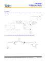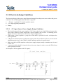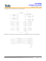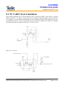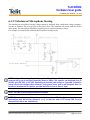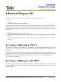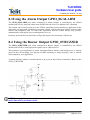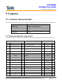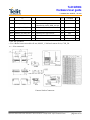
1
Telit GE864
Hardware User guide
1vv0300694, Rev. ISSUE#2, - 19/12/05
Telit
GE864
Hardware User Guide
© Telit Communications S.p.A. 2005
Reproduction forbidden without written authorization of Telit Communications – All Right reserved – Right of modification reserved
page 1 of 60
Telit GE864
Hardware User guide
1vv0300694, Rev. ISSUE#2, - 19/12/05
Contents
1
OVERVIEW
4
2
HARDWARE COMMANDS
5
Turning ON the GE864
5
2.1
2.2
Turning OFF the GE864
2.2.1
Hardware shutdown
7
7
2.3
7
3
3.1
Hardware Unconditional Reboot
POWER SUPPLY
Power Supply Requirements
9
9
3.2
General Design Rules
3.2.1
Electrical design Guidelines
3.2.1.1 + 5V input Source Power Supply Design Guidelines
3.2.1.2 + 12V input Source Power Supply Design Guidelines
3.2.1.3 Battery Source Power Supply Design Guidelines
3.2.1.4 Battery Charge control Circuitry Design Guidelines
3.2.2
Thermal Design Guidelines
3.2.3
Power Supply PCB layout Guidelines
9
10
10
11
12
12
14
14
4
16
ANTENNA
4.1
Antenna Requirements
16
4.2
Antenna PCB line Guidelines
17
4.3
Antenna installation Guidelines
18
5
SERIAL PORT
19
5.1
RS232 level translation
21
5.2
5V UART level translation
23
6
MICROPHONE
25
6.1
Microphone line Characteristic and requirements
25
6.2
General Design Rules
28
Reproduction forbidden without written authorization of Telit Communications – All Right reserved – Right of modification reserved
page 2 of 60
Telit GE864
Hardware User guide
1vv0300694, Rev. ISSUE#2, - 19/12/05
6.3
Microphone Biasing
6.3.1
Balanced Microphone biasing
6.3.2
Unbalanced Microphone biasing
28
29
30
6.4
Microphone buffering
6.4.1
Buffered Balanced Mic.
6.4.2
Buffered Unbalanced (Single Ended) Mic.
31
31
33
7
36
7.1
SPEAKER
Speaker lines characteristics and requirements
36
7.2
General Design rules
7.2.1
Noise Filtering
38
39
7.3
Handset earphone design
39
7.4
Hands Free earphone (low power) design
41
7.5
Car Kit speakerphone design
41
8
GENERAL PURPOSE I/O
43
8.1
Using a GPIO pad as INPUT
43
8.2
Using a GPIO pad as OUTPUT
43
8.3
Using the Alarm Output GPIO_06/ALARM
44
8.4
Using the Buzzer Output GPIO_07/BUZZER
44
9
CAMERA
45
9.1
Camera characteristics
9.1.1
Camera interface connectors
9.1.2
EVB for Transchip camera support
9.1.3
Example usage script for camera
45
45
47
48
10
49
CONFORMITY ASSESSMENT ISSUES
DOCUMENT CHANGE LOG
50
ANNEX A – EVK2 SCHEMATICS
51
ANNEX B - CAMERA EVB SCHEMATICS
57
Reproduction forbidden without written authorization of Telit Communications – All Right reserved – Right of modification reserved
page 3 of 60
Telit GE864
Hardware User guide
1vv0300694, Rev. ISSUE#2, - 19/12/05
1 Overview
The aim of this document is the description of some hardware solutions useful for developing a
product with the Telit GE864 module.
In this document all the basic functions of a mobile phone will be taken into account; for each one
of them a proper hardware solution will be suggested and eventually the wrong solutions and
common errors to be avoided will be evidenced. Obviously this document can not embrace the
whole hardware solutions and products that may be designed. The wrong solutions to be avoided
shall be considered as mandatory, while the suggested hardware configurations shall not be
considered mandatory, instead the information given shall be used as a guide and a starting point for
properly developing your product with the Telit GE864 module. For further hardware details that
may not be explained in this document refer to the Telit GE864 Product Description document
where all the hardware information is reported.
NOTICE
(EN) The integration of the GE864 GSM/GPRS cellular module within user application shall be done according
to the design rules described in this manual.
(IT) L’integrazione del modulo cellulare GSM/GPRS GE864 all’interno dell’applicazione dell’utente dovrà
rispettare le indicazioni progettuali descritte in questo manuale.
(DE) Die Integration des GE864 GSM/GPRS Mobilfunk-Moduls in ein Gerät muß gemäß der in diesem Dokument
beschriebenen Konstruktionsregeln erfolgen
(SL) Integracija GSM/GPRS GE864 modula v uporabniški aplikaciji bo morala upoštevati projektna navodila,
opisana v tem priročniku.
(SP) La utilización del modulo GSM/GPRS GE864 debe ser conforme a los usos para los cuales ha sido
diseñado descritos en este manual del usuario
(FR) L'intégration du module cellulaire GE864 GSM/GPRS dans l'application de l'utilisateur sera faite selon les
règles de conception décrites dans ce manuel
(HE)
The information presented in this document is believed to be accurate and reliable. However, no responsibility is
assumed by Telit Communication for its use, nor any infringement of patents or other rights of third parties which may
result from its use. No license is granted by implication or otherwise under any patent rights of Telit Communication
other than for circuitry embodied in Telit products. This document is subject to change without notice.
Reproduction forbidden without written authorization of Telit Communications – All Right reserved – Right of modification reserved
page 4 of 60
Telit GE864
Hardware User guide
1vv0300694, Rev. ISSUE#2, - 19/12/05
2 Hardware Commands
2.1 Turning ON the GE864
To turn on the GE864 the pad ON# must be tied low for at least 1 second and then released.
The maximum current that can be drained from the ON# pad is 0,1 mA.
A simple circuit to do it is:
ON#
R1
Q1
Power ON impulse
R2
GND
NOTE: don't use any pull up resistor on the ON# line, it is internally pulled up. Using pull up resistor
may bring to latch up problems on the GE864 power regulator and improper power on/off of the
module. The line ON# must be connected only in open collector configuration.
NOTE: In this document all the lines that are inverted, hence have active low signals are labeled with a
name that ends with a "#" or with a bar over the name.
NOTE: The GE864 turns fully on also by supplying power to the Charge pad (provided there's a battery
on the VBATT pads).
Reproduction forbidden without written authorization of Telit Communications – All Right reserved – Right of modification reserved
page 5 of 60
Telit GE864
Hardware User guide
1vv0300694, Rev. ISSUE#2, - 19/12/05
For example:
1- Let's assume you need to drive the ON# pad with a totem pole output of a +3/5 V microcontroller
(uP_OUT1):
2- Let's assume you need to drive the ON# pad directly with an ON/OFF button:
Reproduction forbidden without written authorization of Telit Communications – All Right reserved – Right of modification reserved
page 6 of 60
Telit GE864
Hardware User guide
1vv0300694, Rev. ISSUE#2, - 19/12/05
2.2 Turning OFF the GE864
The turning off of the device can be done in three ways:
•
by software command (see GE864 Software User Guide)
• by hardware shutdown
When the device is shut down by software command or by hardware shutdown, it issues to the
network a detach request that informs the network that the device will not be reachable any more.
2.2.1 Hardware shutdown
To turn OFF the GE864 the pad ON# must be tied low for at least 1 second and then released.
The same circuitry and timing for the power on shall be used.
The device shuts down after the release of the ON# pad.
TIP: To check if the device has powered off, the hardware line PWRCTL should be monitored. When
PWRCTL goes low, the device has powered off.
2.3 Hardware Unconditional Reboot
To unconditionally Reboot the GE864, the pad RESET# must be tied low for at least 200
milliseconds and then released.
The maximum current that can be drained from the ON# pad is 0,15 mA.
A simple circuit to do it is:
RESET#
Unconditional Reboot
impulse
GND
Reproduction forbidden without written authorization of Telit Communications – All Right reserved – Right of modification reserved
page 7 of 60
Telit GE864
Hardware User guide
1vv0300694, Rev. ISSUE#2, - 19/12/05
NOTE: don't use any pull up resistor on the RESET# line nor any totem pole digital output. Using pull
up resistor may bring to latch up problems on the GE864 power regulator and improper functioning of
the module. The line RESET# must be connected only in open collector configuration.
TIP: The unconditional hardware reboot should be always implemented on the boards and software
should use it as an emergency exit procedure.
For example:
1- Let's assume you need to drive the RESET# pad with a totem pole output of a +3/5 V
microcontroller (uP_OUT2):
Reproduction forbidden without written authorization of Telit Communications – All Right reserved – Right of modification reserved
page 8 of 60
Telit GE864
Hardware User guide
1vv0300694, Rev. ISSUE#2, - 19/12/05
3 Power Supply
The power supply circuitry and board layout are a very important part in the full product design and
they strongly reflect on the product overall performances, hence read carefully the requirements and
the guidelines that will follow for a proper design.
3.1 Power Supply Requirements
The GE864 power requirements are:
•
Nominal Supply Voltage:
3.8 V
•
Max Supply Voltage:
4.2 V
•
Supply voltage range:
3.4 V - 4.2 V
•
Max Peak current consumption (impulsive):
1.9 A
•
Max Average current consumption during GPRS transmission (rms):
500 mA
•
Max Average current consumption during VOICE/CSD transmission (rms):
270 mA
•
Average current during Power Saving:
≈ 4 mA
•
Average current during idle (Power Saving disabled)
≈ 19 mA
The GSM system is made in a way that the RF transmission is not continuous, else it is packed into
bursts at a base frequency of about 216 Hz, the relative current peaks can be as high as about 2A.
Therefore the power supply has to be designed in order to withstand with these current peaks
without big voltage drops; this means that both the electrical design and the board layout must be
designed for this current flow.
If the layout of the PCB is not well designed a strong noise floor is generated on the ground and the
supply; this will reflect on all the audio paths producing an audible annoying noise at 216 Hz; if the
voltage drop during the peak current absorption is too much, then the device may even shutdown as
a consequence of the supply voltage drop.
TIP: The electrical design for the Power supply should be made ensuring it will be capable of a peak
current output of at least 2 A.
3.2 General Design Rules
The principal guidelines for the Power Supply Design embrace three different design steps:
- the electrical design
- the thermal design.
- the PCB layout.
Reproduction forbidden without written authorization of Telit Communications – All Right reserved – Right of modification reserved
page 9 of 60
Telit GE864
Hardware User guide
1vv0300694, Rev. ISSUE#2, - 19/12/05
3.2.1 Electrical design Guidelines
The electrical design of the power supply depends strongly from the power source where this power
is drained. We will distinguish them into three categories:
•
+5V input (typically PC internal regulator output)
•
+12V input (typically automotive)
•
Battery
3.2.1.1 + 5V input Source Power Supply Design Guidelines
•
The desired output for the power supply is 3.8V, hence there's not a big difference between the
input source and the desired output and a linear regulator can be used. A switching power
supply will not be suited because of the low drop out requirements.
•
When using a linear regulator, a proper heat sink shall be provided in order to dissipate the
power generated.
•
A Bypass low ESR capacitor of adequate capacity must be provided in order to cut the current
absorption peaks close to the GE864, a 100μF tantalum capacitor is usually suited.
•
Make sure the low ESR capacitor on the power supply output (usually a tantalum one) is rated
at least 10V.
•
A protection diode should be inserted close to the power input, in order to save the GE864 from
power polarity inversion.
An example of linear regulator with 5V input is:
Reproduction forbidden without written authorization of Telit Communications – All Right reserved – Right of modification reserved
page 10 of 60
Telit GE864
Hardware User guide
1vv0300694, Rev. ISSUE#2, - 19/12/05
3.2.1.2 + 12V input Source Power Supply Design Guidelines
•
The desired output for the power supply is 3.8V, hence due to the big difference between the
input source and the desired output, a linear regulator is not suited and shall not be used. A
switching power supply will be preferable because of its better efficiency especially with the 2A
peak current load represented by the GE864.
•
When using a switching regulator, a 500kHz or more switching frequency regulator is
preferable because of its smaller inductor size and its faster transient response. This allows the
regulator to respond quickly to the current peaks absorption.
•
For car PB battery the input voltage can rise up to 15,8V and this should be kept in mind when
choosing components: all components in the power supply must withstand this voltage.
•
A Bypass low ESR capacitor of adequate capacity must be provided in order to cut the current
absorption peaks, a 100μF tantalum capacitor is usually suited.
•
Make sure the low ESR capacitor on the power supply output (usually a tantalum one) is rated
at least 10V.
•
For Car applications a spike protection diode should be inserted close to the power input, in
order to clean the supply from spikes.
•
A protection diode should be inserted close to the power input, in order to save the GE864 from
power polarity inversion. This can be the same diode as for spike protection.
An example of switching regulator with 12V input is:
Reproduction forbidden without written authorization of Telit Communications – All Right reserved – Right of modification reserved
page 11 of 60
Telit GE864
Hardware User guide
1vv0300694, Rev. ISSUE#2, - 19/12/05
3.2.1.3 Battery Source Power Supply Design Guidelines
•
The desired nominal output for the power supply is 3.8V and the maximum voltage allowed is
4.2V, hence a single 3.7V Li-Ion cell battery type is suited for supplying the power to the Telit
GE864 module.
The three cells Ni/Cd or Ni/MH 3,6 V Nom. battery types or 4V PB types MUST NOT BE
USED DIRECTLY since their maximum voltage can rise over the absolute maximum voltage
for the GE864 and damage it.
NOTE: DON'T USE any Ni-Cd, Ni-MH, and Pb battery types directly connected with GE864. Their use
can lead to overvoltage on the GE864 and damage it. USE ONLY Li-Ion battery types.
•
A Bypass low ESR capacitor of adequate capacity must be provided in order to cut the current
absorption peaks, a 100μF tantalum capacitor is usually suited.
•
Make sure the low ESR capacitor (usually a tantalum one) is rated at least 10V.
•
A protection diode should be inserted close to the power input, in order to save the GE864 from
power polarity inversion. Otherwise the battery connector should be done in a way to avoid
polarity inversions when connecting the battery.
•
The battery capacity must be at least 500mAh in order to withstand the current peaks of 2A; the
suggested capacity is from 500mAh to 1000mAh.
3.2.1.4 Battery Charge control Circuitry Design Guidelines
The charging process for Li-Ion Batteries can be divided into 4 phases:
•
Qualification and trickle charging
•
Fast charge 1 - constant current
•
Final charge - constant voltage or pulsed charging
• Maintenance charge
The qualification process consists in a battery voltage measure, indicating roughly its charge status.
If the battery is deeply discharged, that means its voltage is lower than the trickle charging
threshold, then the charge must start slowly possibly with a current limited pre-charging process
where the current is kept very low with respect to the fast charge value: the trickle charging.
During the trickle charging the voltage across the battery terminals rises; when it reaches the fast
charge threshold level the charging process goes into fast charge phase.
During the fast charge phase the process proceeds with a current limited charging; this current limit
depends on the required time for the complete charge and from the battery pack capacity. During
this phase the voltage across the battery terminals still raises but at a lower rate.
Once the battery voltage reaches its maximum voltage then the process goes into its third state:
Final charging. The voltage measure to change the process status into final charge is very
important. It must be ensured that the maximum battery voltage is never exceeded, otherwise the
battery may be damaged and even explode. Moreover for the constant voltage final chargers, the
constant voltage phase (final charge) must not start before the battery voltage has reached its
maximum value, otherwise the battery capacity will be highly reduced.
Reproduction forbidden without written authorization of Telit Communications – All Right reserved – Right of modification reserved
page 12 of 60
Telit GE864
Hardware User guide
1vv0300694, Rev. ISSUE#2, - 19/12/05
The final charge can be of two different types: constant voltage or pulsed. GE864 uses constant
voltage.
The constant voltage charge proceeds with a fixed voltage regulator (very accurately set to the
maximum battery voltage) and hence the current will decrease while the battery is becoming
charged. When the charging current falls below a certain fraction of the fast charge current value,
then the battery is considered fully charged, the final charge stops and eventually starts the
maintenance.
The pulsed charge process has no voltage regulation, instead the charge continues with pulses.
Usually the pulse charge works in the following manner: the charge is stopped for some time, let's
say few hundreds of ms, then the battery voltage will be measured and when it drops below its
maximum value a fixed time length charging pulse is issued. As the battery approaches its full
charge the off time will become longer, hence the duty-cycle of the pulses will decrease. The
battery is considered fully charged when the pulse duty-cycle is less than a threshold value,
typically 10%, the pulse charge stops and eventually the maintenance starts.
The last phase is not properly a charging phase, since the battery at this point is fully charged and
the process may stop after the final charge. The maintenance charge provides an additional charging
process to compensate for the charge leak typical of a Li-Ion battery. It is done by issuing pulses
with a fixed time length, again few hundreds of ms, and a duty-cycle around 5% or less.
This last phase is not implemented in the GE864 internal charging algorithm, so that the battery
once charged is left discharging down to a certain threshold so that it is cycled from full charge to
slight discharge even if the battery charger is always inserted. This guarantees that anyway the
remaining charge in the battery is a good percentage and that the battery is not damaged by keeping
it always fully charged (Li-Ion rechargeable battery usually deteriorate when kept fully charged).
Last but not least, in some applications it is highly desired that the charging process restarts when
the battery is discharged and its voltage drops below a certain threshold, GE864 internal charger
does it.
As you can see, the charging process is not a trivial task to be done; moreover all these operations
should start only if battery temperature is inside a charging range, usually 5°C - 45°C.
The GE864 measures the temperature of its internal component, in order to satisfy this last
requirement, it's not exactly the same as the battery temperature but in common application the two
temperature should not differ too much and the charging temperature range should be guaranteed.
NOTE: For all the threshold voltages, inside the GE864 all threshold are fixed in order to maximize LiIon battery performances and do not need to be changed.
NOTE: In this application the battery charger input current must be limited to less than 400mA. This
can be done by using a current limited wall adapter as the power source.
Reproduction forbidden without written authorization of Telit Communications – All Right reserved – Right of modification reserved
page 13 of 60
Telit GE864
Hardware User guide
1vv0300694, Rev. ISSUE#2, - 19/12/05
3.2.2Thermal Design Guidelines
The thermal design for the power supply heat sink should be done with the following specifications:
•
Average current consumption during transmission @PWR level max (rms): 500mA
•
Average current consumption during transmission @ PWR level min (rms): 100mA
•
Average current during Power Saving:
4mA
•
Average current during idle (Power Saving disabled)
19mA
NOTE: The average consumption during transmissions depends on the power level at which the
device is requested to transmit by the network. The average current consumption hence varies
significantly.
TIP: The thermal design for the Power supply should be made keeping a average consumption at the
max transmitting level during calls of 500mA rms.
Considering the very low current during idle, especially if Power Saving function is enabled, it is
possible to consider from the thermal point of view that the device absorbs current significantly
only during calls.
If we assume that the device stays into transmission for short periods of time (let's say few minutes)
and then remains for a quite long time in idle (let's say one hour), then the power supply has always
the time to cool down between the calls and the heat sink could be smaller than the calculated one
for 500mA maximum RMS current, or even could be the simple chip package (no heat sink).
Moreover in the average network conditions the device is requested to transmit at a lower power
level than the maximum and hence the current consumption will be less than the 500mA, being
usually around 150mA.
For these reasons the thermal design is rarely a concern and the simple ground plane where the
power supply chip is placed can be enough to ensure a good thermal condition and avoid
overheating.
For the heat generated by the GE864, you can consider it to be during transmission 1W max during
CSD/VOICE calls and 2W max during class10 GPRS upload.
This generated heat will be mostly conducted to the ground plane under the GE864, you must
ensure that your application can dissipate it.
3.2.3 Power Supply PCB layout Guidelines
As seen on the electrical design guidelines the power supply shall have a low ESR capacitor on the
output to cut the current peaks and a protection diode on the input to protect the supply from spikes
and polarity inversion. The placement of these components is crucial for the correct working of the
circuitry. A misplaced component can be useless or can even decrease the power supply
performances.
Reproduction forbidden without written authorization of Telit Communications – All Right reserved – Right of modification reserved
page 14 of 60
Telit GE864
Hardware User guide
1vv0300694, Rev. ISSUE#2, - 19/12/05
•
The Bypass low ESR capacitor must be placed close to the Telit GE864 power input pads or in
the case the power supply is a switching type it can be placed close to the inductor to cut the
ripple provided the PCB trace from the capacitor to the GE864 is wide enough to ensure a
dropless connection even during the 2A current peaks.
•
The protection diode must be placed close to the input connector where the power source is
drained.
•
The PCB traces from the input connector to the power regulator IC must be wide enough to
ensure no voltage drops occur when the 2A current peaks are absorbed. Note that this is not
made in order to save power loss but especially to avoid the voltage drops on the power line at
the current peaks frequency of 216 Hz that will reflect on all the components connected to that
supply, introducing the noise floor at the burst base frequency. For this reason while a voltage
drop of 300-400 mV may be acceptable from the power loss point of view, the same voltage
drop may not be acceptable from the noise point of view. If your application doesn't have audio
interface but only uses the data feature of the Telit GE864, then this noise is not so disturbing
and power supply layout design can be more forgiving.
•
The PCB traces to the GE864 and the Bypass capacitor must be wide enough to ensure no
significant voltage drops occur when the 2A current peaks are absorbed. This is for the same
reason as previous point. Try to keep this trace as short as possible.
•
The PCB traces connecting the Switching output to the inductor and the switching diode must
be kept as short as possible by placing the inductor and the diode very close to the power
switching IC (only for switching power supply). This is done in order to reduce the radiated
field (noise) at the switching frequency (100-500 kHz usually).
•
The use of a good common ground plane is suggested.
•
The placement of the power supply on the board should be done in such a way to guarantee that
the high current return paths in the ground plane are not overlapped to any noise sensitive
circuitry as the microphone amplifier/buffer or earphone amplifier.
•
The power supply input cables should be kept separate from noise sensitive lines such as
microphone/earphone cables.
Reproduction forbidden without written authorization of Telit Communications – All Right reserved – Right of modification reserved
page 15 of 60
Telit GE864
Hardware User guide
1vv0300694, Rev. ISSUE#2, - 19/12/05
4 Antenna
The antenna connection and board layout design are the most important part in the full product
design and they strongly reflect on the product overall performances, hence read carefully and
follow the requirements and the guidelines for a proper design.
4.1 Antenna Requirements
As suggested on the Product Description the antenna and antenna line on PCB for a Telit GE864
device shall fulfil the following requirements:
ANTENNA REQUIREMENTS
Frequency range
Standard Dual Band GSM/DCS frequency
range or
Standard Tri Band GSM/DCS/PCS frequency
range if used for all three bands
Bandwidth
80 MHz in GSM & 170 MHz in DCS & 140
MHz PCS band
Gain
Gain < 3dBi
Impedance
50 ohm
Input power
> 2 W peak power
VSWR absolute
max
<= 10:1
VSWR
recommended
<= 2:1
When using the Telit GE864, since there's no antenna connector on the module, the antenna must be
connected to the GE864 through the PCB with the antenna pad.
In the case that the antenna is not directly developed on the same PCB, hence directly connected at
the antenna pad of the GE864, then a PCB line is needed in order to connect with it or with its
connector.
Reproduction forbidden without written authorization of Telit Communications – All Right reserved – Right of modification reserved
page 16 of 60
Telit GE864
Hardware User guide
1vv0300694, Rev. ISSUE#2, - 19/12/05
This line of transmission shall fulfil the following requirements:
ANTENNA LINE ON PCB REQUIREMENTS
Impedance
50 ohm
Max Attenuation
0,3 dB
No coupling with other signals allowed
Cold End (Ground Plane) of antenna shall be equipotential to
the GE864 ground pins
Furthermore if the device is developed for the US market and/or Canada market, it shall comply to
the FCC and/or IC approval requirements:
This device is to be used only for mobile and fixed application. The antenna(s) used for this
transmitter must be installed to provide a separation distance of at least 20 cm from all persons and
must not be co-located or operating in conjunction with any other antenna or transmitter. EndUsers must be provided with transmitter operation conditions for satisfying RF exposure
compliance. OEM integrators must ensure that the end user has no manual instructions to remove
or install the GE864 module. Antennas used for this OEM module must not exceed 3dBi gain for
mobile and fixed operating configurations.
4.2 Antenna PCB line Guidelines
•
Ensure that the antenna line impedance is 50 ohm;
•
Keep the antenna line on the PCB as short as possible, since the antenna line loss shall be less
than 0,3 dB;
•
Antenna line must have uniform characteristics, constant cross section, avoid meanders and
abrupt curves;
•
Keep, if possible, one layer of the PCB used only for the Ground plane;
•
Surround (on the sides, over and under) the antenna line on PCB with Ground, avoid having
other signal tracks facing directly the antenna line track;
•
The ground around the antenna line on PCB has to be strictly connected to the Ground Plane by
placing vias once per 2mm at least;
•
Place EM noisy devices as far as possible from GE864 antenna line;
•
Keep the antenna line far away from the GE864 power supply lines;
•
If you have EM noisy devices around the PCB hosting the GE864, such as fast switching ICs,
take care of the shielding of the antenna line by burying it inside the layers of PCB and
surround it with Ground planes, or shield it with a metal frame cover.
•
If you don't have EM noisy devices around the PCB of GE864, by using a strip-line on the
superficial copper layer for the antenna line, the line attenuation will be lower than a buried one;
Reproduction forbidden without written authorization of Telit Communications – All Right reserved – Right of modification reserved
page 17 of 60
Telit GE864
Hardware User guide
1vv0300694, Rev. ISSUE#2, - 19/12/05
4.3 Antenna installation Guidelines
•
Install the antenna in a place covered by the GSM signal.
•
The Antenna must be installed to provide a separation distance of at least 20 cm from all
persons and must not be co-located or operating in conjunction with any other antenna or
transmitter;
•
Antenna shall not be installed inside metal cases
•
Antenna shall be installed also according Antenna manufacturer instructions.
Reproduction forbidden without written authorization of Telit Communications – All Right reserved – Right of modification reserved
page 18 of 60
Telit GE864
Hardware User guide
1vv0300694, Rev. ISSUE#2, - 19/12/05
5 Serial Port
The serial port on the Telit GE864 is the core of the interface between the module and OEM
hardware. Several configurations can be designed for the serial port on the OEM hardware, but the
most common are:
- RS232 PC com port
- microcontroller UART @ 2.8V - 3V (Universal Asynchronous Receive Transmit)
- microcontroller UART@ 5V or other voltages different from 2.8V
Depending from the type of serial port on the OEM hardware a level translator circuit may be
needed to make the system work. The only configuration that doesn't need a level translation is the
2.8V UART.
The serial port on the GE864 is a +2.8V UART with all the 7 RS232 signals. It differs from the PCRS232 in the signal polarity (RS232 is reversed) and levels. The levels for the GE864 UART are
the CMOS levels:
Absolute Maximum Ratings -Not Functional
Parameter
Min
Max
Input level on any
digital pad when on
-0.3V
+3.75V
Input voltage on
-0.3V
analog pads when on
+3.0 V
Operating Range - Interface levels (2.8V CMOS)
Level
Min
Max
Input high level VIH 2.1V
3.3V
Input low level
0.5V
VIL 0V
Output high level VOH 2.2V
3.0V
Output low level VOL 0V
0.35V
Reproduction forbidden without written authorization of Telit Communications – All Right reserved – Right of modification reserved
page 19 of 60
Telit GE864
Hardware User guide
1vv0300694, Rev. ISSUE#2, - 19/12/05
The signals of the GE864 serial port are:
RS232
Pin
Number
Signal
GE864 Pad
Number
Name
Usage
1
DCD dcd_uart
42
Data Carrier Detect
Output from the GE864 that indicates the
carrier presence
2
RXD tx_uart
38
Transmit line *see Note
Output transmit line of GE864 UART
3
TXD rx_uart
37
Receive line *see Note
Input receive of the GE864 UART
4
DTR dtr_uart
39
Data Terminal Ready
Input to the GE864 that controls the DTE
READY condition
5
GND
8-17-28-3645-48-50-56
Ground
ground
6
DSR dsr_uart
43
Data Set Ready
Output from the GE864 that indicates the
module is ready
7
RTS rts_uart
40
Request to Send
Input to the GE864 that controls the
Hardware flow control
8
CTS cts_uart
41
Clear to Send
Output from the GE864 that controls the
Hardware flow control
9
RI ri_uart
44
Ring Indicator
Output from the GE864 that indicates the
incoming call condition
NOTE: According to V.24, RX/TX signal names are referred to the application side, therefore on the
GE864 side these signal are on the opposite direction: TXD on the application side will be connected
to the receive line (here named TXD/ rx_uart ) of the GE864 serial port and viceversa for RX.
TIP: For a minimum implementation, only the TXD and RXD lines can be connected, the other lines can
be left open provided a software flow control is implemented.
The signals in the UART connector on the EVK2 are:
DCD
RXD
TXD
DTR
GND
DSR
RTS
CTS
RI
GND
Reproduction forbidden without written authorization of Telit Communications – All Right reserved – Right of modification reserved
page 20 of 60
Telit GE864
Hardware User guide
1vv0300694, Rev. ISSUE#2, - 19/12/05
5.1 RS232 level translation
In order to interface the Telit GE864 with a PC com port or a RS232 (EIA/TIA-232) application a
level translator is required. This level translator must
- invert the electrical signal in both directions
- change the level from 0/3V to +15/-15V
Actually, the RS232 UART 16450, 16550, 16650 & 16750 chipsets accept signals with lower levels
on the RS232 side (EIA/TIA-562) , allowing for a lower voltage-multiplying ratio on the level
translator. Note that the negative signal voltage must be less than 0V and hence some sort of level
translation is always required.
The simplest way to translate the levels and invert the signal is by using a single chip level
translator. There are a multitude of them, differing in the number of driver and receiver and in the
levels (be sure to get a true RS232 level translator not a RS485 or other standards).
By convention the driver is the level translator from the 0-3V UART level to the RS232 level, while
the receiver is the translator from RS232 level to 0-3V UART.
In order to translate the whole set of control lines of the UART you will need:
- 5 driver
- 3 receiver
NOTE: The digital input lines working at 2.8VCMOS have an absolute maximum input voltage of 3,75V;
therefore the level translator IC shall not be powered by the +3.8V supply of the module. Instead it
shall be powered from a +2.8V / +3.0V (dedicated) power supply.
This is because in this way the level translator IC outputs on the module side (i.e. GE864 inputs) will
work at +3.8V interface levels, stressing the module inputs at its maximum input voltage.
This can be acceptable for evaluation purposes, but not on production devices.
NOTE: In order to be able to do in circuit reprogramming of the GE864 firmware, the serial port on the
Telit GE864 shall be available for translation into RS232 and either it's controlling device shall be
placed into tristate, disconnected or as a gateway for the serial data when module reprogramming
occurs.
Only RXD, TXD, GND and the On/off module turn on pad are required to the reprogramming of the
module, the other lines are unused.
All applicator shall include in their design such a way of reprogramming the GE864.
Reproduction forbidden without written authorization of Telit Communications – All Right reserved – Right of modification reserved
page 21 of 60
Telit GE864
Hardware User guide
1vv0300694, Rev. ISSUE#2, - 19/12/05
An example of level translation circuitry of this kind is:
the RS232 serial port lines are usually connected to a DB9 connector with the following layout:
Reproduction forbidden without written authorization of Telit Communications – All Right reserved – Right of modification reserved
page 22 of 60
Telit GE864
Hardware User guide
1vv0300694, Rev. ISSUE#2, - 19/12/05
5.2 5V UART level translation
If the OEM application uses a microcontroller with a serial port (UART) that works at a voltage
different from 2.8 - 3V, then a circuitry has to be provided to adapt the different levels of the two
set of signals. As for the RS232 translation there are a multitude of single chip translators, but since
the translation requires very few components, then also a discrete design can be suited. For example
a possible inexpensive translator circuit for a 5V driver can be:
and for a 5V receiver:
Reproduction forbidden without written authorization of Telit Communications – All Right reserved – Right of modification reserved
page 23 of 60
Telit GE864
Hardware User guide
1vv0300694, Rev. ISSUE#2, - 19/12/05
NOTE: The UART input line TXD (rx_uart) of the GE864 is NOT internally pulled up with a resistor, so
there may be the need to place an external 47KΩ pull-up resistor, either the DTR (dtr_uart) and RTS
(rts_uart) input lines are not pulled up internally, so an external pull-up resistor of 47KΩ may be
required.
A power source of the internal interface voltage corresponding to the 2.8VCMOS high level is
available at the VAUX pad, whose absolute maximum output current is 100mA.
Pull-up resistors can be connected to the VAUX pad provided that the pulled-up lines are GE864
input lines connected to open collector outputs in order to avoid latch-up problems on the GE864.
Care must be taken to avoid latch-up on the GE864 and the use of this output line to power
electronic devices shall be considered with care, especially for devices that generate spikes and
noise such as level translators, digital ICs or microcontroller, failure in any of these condition can
severely compromise the GE864 functionality.
NOTE: The input lines working at 2.8VCMOS can be pulled-up with 47KΩ resistors that can be
connected directly to the VAUX line.
NO disturbing devices should be powered with the VAUX line, otherwise the module functionality may
be compromised.
Reproduction forbidden without written authorization of Telit Communications – All Right reserved – Right of modification reserved
page 24 of 60
Telit GE864
Hardware User guide
1vv0300694, Rev. ISSUE#2, - 19/12/05
6 Microphone
The microphone circuitry is the more noise sensitive and its design and layout must be done with
particular care.
6.1 Microphone line Characteristic and
requirements
The Telit GE864 provides two audio paths for the microphone and the earpiece: the internal and the
external audio paths. Only one of the two paths can be active at a time and it is selectable by
hardware line AXE or by AT command. The audio characteristics of the two paths are slightly
different and this should be kept in mind when designing. The internal audio path should be used
for handset function, while the external audio path is suited for hands free function (car kit).
Both microphone paths from the Telit GE864 are balanced and the OEM circuitry should be
designed balanced to reduce the common mode noise typically generated on the ground plane,
however for particular OEM application needs also an unbalanced circuitry can be used.
The microphone input lines characteristics are:
internal microphone path
•
line coupling:
AC ( 100nF cond.)
•
line type:
balanced
•
differential input resistance:
25kΩ
•
line nominal sensitivity:
50 mVrms
•
max input voltage:
360 mVrms
•
microphone nominal sensitivity/analog gain suggested:
-45 dBVrms/Pa / +24dB
•
echo canceller type:
handset
external microphone path
•
line coupling:
AC ( 100nF cond.)
•
line type:
balanced
•
differential input resistance:
25kΩ
•
line nominal sensitivity:
3 mVrms
•
max input voltage:
22 mVrms
•
microphone nominal sensitivity/analog gain suggested:
-45 dBVrms/Pa / +10dB
•
echo canceller type:
car kit hands free
Reproduction forbidden without written authorization of Telit Communications – All Right reserved – Right of modification reserved
page 25 of 60
Telit GE864
Hardware User guide
1vv0300694, Rev. ISSUE#2, - 19/12/05
TIP: Due to the difference in the echo canceller type, the internal audio path is suited for handset
applications while the external audio path is suited for car kit hands free. The headset applications
should be made by using the external audio path but DISABLING the echo canceller by software AT
command. If the echo canceller is left active with the headset, then some echo might be introduced by
the echo cancel algorithm.
The nominal sensitivity of the line indicates the voltage level on the GE864 pads that should be
present during "normal spoken" conditions: for a handset a voice signal coming from the mouth of
the talker at 7 cm of distance from the microphone, producing an acoustic pressure of -4,7 dBPa (@
1 kHz) on the microphone membrane.
For example:
With the internal mic. having the suggested nominal sensitivity -45dBVrms/Pa
at the "normal spoken" conditions: -4.7dB Pa on the microphone membrane.
At that acoustic pressure the voltage output from the microphone is:
Voltage Output (dB) = ( -45) + (-4.7) = -49.7 dBVrms
corresponding to:
Voltage Output = 10 ( -49.7 / 20 ) = 3.3* 10 -3 Vrms
by having the microphone gain set to +24 dB (corresponding to 15.8 times) the signal in the
nominal conditions on the input mic. pads of the GE864 will be:
Voltage @ GE864_mic = 3.3 * 10 -3 * 15.8 = 51 mVrms
During the spoken conditions the signal varies according to the volume of the voice of the talker,
usually a rough thumb rule for the dynamic range may be considered:
* +20dB (10 times) at maximum voice level (talker screaming)
* -50 dB (1/300 times) at minimum voice level (talker whispering).
For the handsfree/car kit microphone the voice attenuation due to the distance between the
microphone and the talker must be taken into account when designing the microphone amplifier.
For a car cabin usually the distance between the talker and the mic. is about 50cm; in these
conditions the attenuation can be considered as a thumb rule around 20dB.
Another thing to consider, especially for cabin car use, is the fact that the external mic. will pick up
also ambient noise; to overcome this problem it is preferable to set the gain of the microphone 10dB
lower with respect to the calculated value for a nominal sensitivity. The corresponding reduction in
signal level will be compensated by an increased voice volume of the talker which will speak louder
because of the ambient noise.
Reproduction forbidden without written authorization of Telit Communications – All Right reserved – Right of modification reserved
page 26 of 60
Telit GE864
Hardware User guide
1vv0300694, Rev. ISSUE#2, - 19/12/05
For the headset we shall distinguish two different types: the headsets having the microphone
sustained close to the mouth and the headsets having the microphone on the earpiece cable.
The same considerations for the additional voice attenuation due to the distance from the
microphone and the noise pick up can be made for the headset having the microphone on the
earpiece cable, while the other kind of headset shall be threaten as an handset.
For example:
With the external mic. having the suggested nominal sensitivity -45dBVrms/Pa
at the "normal spoken" conditions: -4.7dB Pa at 7 cm from the mouth of the talker and with a
further attenuation of 20dB due to the distance from the microphone (about 50 cm).
At that acoustic pressure the voltage output from the microphone is:
Voltage Output (dB) = ( -45) + (-4.7) - 20 = -69.7 dBVrms
corresponding to:
Voltage Output = 10 ( -69.7 / 20 ) = 3.3* 10 -4 Vrms
by having the microphone gain set to +10 dB (corresponding to 3 times) the signal in the nominal
conditions on the input external mic. pads of the GE864 will be:
Voltage @ GE864__extmic = 3.3 * 10 -4 * 3 = 1 mVrms
Hence in these conditions the signal level on the input pads of the external mic. of the GE864 is 10
dB (3 times) lower than the nominal, as suggested.
The microphones usually need a biasing network that provides the necessary DC current to the mic.,
this will be explained further on.
In the EVK2 all the microphone input jacks have the hot wire connected to the central pole.
Reproduction forbidden without written authorization of Telit Communications – All Right reserved – Right of modification reserved
page 27 of 60
Telit GE864
Hardware User guide
1vv0300694, Rev. ISSUE#2, - 19/12/05
6.2 General Design Rules
There are several configurations for the audio path, but the most effective difference is between
balanced and unbalanced microphone.
It is highly recommended to keep the whole microphone path balanced even if this means having 2
wires connecting the microphone instead of one needed (plus ground) in the unbalanced case. The
balanced circuitry is more suited because of its good common mode noise rejection, reducing the
216 Hz burst noise produced during the GSM transmissions.
•
Where possible use balanced microphone circuitry
•
Keep the microphone traces on the PCB and wires as short as possible.
•
If your application requires an unbalanced microphone, then keep the lines on the PCB
balanced and "unbalance" the path close to the microphone wire connector if possible.
•
For the microphone biasing voltage use a dedicated voltage regulator and a capacitor multiply
circuit.
•
Make sure that the microphone traces in the PCB don't cross or run parallel to noisy traces
(especially the power line)
•
If possible put all around to the microphone lines a ground trace connected to the ground plane
by several vias. This is done in order to simulate a shielded trace on the PCB.
•
The biasing circuit and eventually the buffer can be designed in the same manner for the
internal and external microphones.
6.3 Microphone Biasing
The electret microphones usually need a biasing voltage to work properly. Refer to your
microphone provider for the characteristics required.
NOTE: The microphones have a hot wire were the positive biasing must be connected, usually it is
indicated by a + sign or a red point. If the polarity of the bias is reversed, then the microphone will not
work properly. For this reason be sure to respect the mic. biasing polarity.
Reproduction forbidden without written authorization of Telit Communications – All Right reserved – Right of modification reserved
page 28 of 60
Telit GE864
Hardware User guide
1vv0300694, Rev. ISSUE#2, - 19/12/05
6.3.1 Balanced Microphone biasing
The balanced microphone bias voltage should be obtained from a dedicated voltage regulator, in
order to eliminate the noise present on the power lines. This regulator can be the same for all the
audio paths. The microphone should be supplied from a capacitor multiply circuit.
For example a circuit for the balanced microphone biasing can be:
NOTE: In the balanced application the resistors R2 and R3 must have the same value to keep the
circuit balanced.
NOTE: The cable to the microphone should not be shielded, instead a twisted pair cable shall be used.
NOTE: The microphone sensitivity changes with the value of R2 and R3. Usually the microphones are
characterized with 2kΩ biasing resistance, so try to keep the sum of R2 and R3 around 2kΩ. Refer to
your microphone manufacturer for the mic. characteristics.
Reproduction forbidden without written authorization of Telit Communications – All Right reserved – Right of modification reserved
page 29 of 60
Telit GE864
Hardware User guide
1vv0300694, Rev. ISSUE#2, - 19/12/05
6.3.2 Unbalanced Microphone biasing
The unbalanced microphone biasing voltage should be obtained from a dedicated voltage regulator,
in order to eliminate the noise present on the power lines. This regulator can be the same for all the
audio paths. The microphone should be supplied from a capacitor multiply circuit.
For example a circuit for the unbalanced microphone biasing can be:
NOTE: In the unbalanced application the capacitor C3 shall be > 200nF otherwise the frequency
response will be cut at low band frequencies (down to 300Hz). This capacitor can be placed close to
the MIC- pad (EXT_MIC- or INT_MIC- depending on the audio path chosen) or if possible it should be
placed close to the shielded cable connector. If the ground return path is well designed, then it is
possible to eliminate the C3 capacitor, provided the buffer is close to the mic. input.
NOTE: The cable to the microphone should be shielded.
NOTE: The microphone sensitivity changes with the value of R2. Usually the microphones are
characterized with 2kΩ biasing resistance, so try to keep the value of R2 around 2kΩ. For mic.
characteristics refer to the manufacturer.
Reproduction forbidden without written authorization of Telit Communications – All Right reserved – Right of modification reserved
page 30 of 60
Telit GE864
Hardware User guide
1vv0300694, Rev. ISSUE#2, - 19/12/05
6.4 Microphone buffering
As seen previously, a microphone shall be connected to the input pads of the GE864 through a
buffer amplifier that boosts the signal level to the required value.
Again the buffered microphone circuitry can be balanced or unbalanced. Where possible it is
always preferable a balanced mic. solution. The buffering circuit shall be placed close to the
microphone or close to the microphone wire connector.
6.4.1 Buffered Balanced Mic.
A sample circuit can be:
This circuit has a gain of 15 times (+24 dB), and is therefore suited for the internal mic. input,
having a microphone with a sensitivity close to the suggested one (-45 dBVrms/Pa), if the used
microphone has a different sensitivity, or if the buffer is connected to the external mic. input, then a
gain adjustment shall be done by changing resistors R604-R605 and R606-R607 and as a
consequence the capacitors C636 and C637 to maintain the bandwidth 150-8000 (-3dB).
The buffer gain is given by the formula:
Gain =
R604 R606
=
R605 R607
The C636 and C637 capacitors are placed in order to cut off the gain at higher frequencies than the
transmitted GSM band, the cutoff frequency (-3dB) should be 8 kHz in order to have -1dB at 4kHz.
Reproduction forbidden without written authorization of Telit Communications – All Right reserved – Right of modification reserved
page 31 of 60
Telit GE864
Hardware User guide
1vv0300694, Rev. ISSUE#2, - 19/12/05
The cutoff frequency is given by the formula:
freq. =
1
1
=
[Hz]
2π * R 604 * C 637 2π * R606 * C 636
For example:
- Let's assume you have a microphone with these characteristics:
- sensitivity -45 dBVrms/Pa
and you want to use it in the internal mic. audio path.
With the mic. having nominal sensitivity -45dBVrms/Pa at the "normal spoken" conditions: -4.7dB Pa
at 7 cm from the mouth of the talker.
At that acoustic pressure the voltage output from the microphone is:
Mic Voltage Output (dB) = ( -45) + (-4.7) = -49.7 dBVrms
corresponding to:
Mic_Voltage_Output = 10 ( -49.7 / 20 ) = 3.3* 10 -3 Vrms
in order to have a signal of 50 mVrms on the GE864 internal mic. inputs then the buffer must have a
gain of:
Voltage @ GE864_intmic/ Mic_Voltage_Output = (50 * 10 -3 )/( 3.3 * 10 -3 ) = 15
Hence in these conditions the signal level on the input pads of the internal mic. of the GE864 is 24
dB (15 times) higher than the microphone output and therefore the buffer has to gain 24 dB.
The corresponding values for the resistors on the buffer could be ( if we keep the input resistance
10kΩ )
R604 = R606 = gain* R603= gain* R605 = 15* 10 = 150 kΩ
The commercial values of 150kΩ & 10kΩ are then chosen.
As a consequence the values of the capacitors C636 and C637 shall be:
C636=C637= 1/ (2π*8000*R606)= 132 *10 -12 F
A commercial value of 100pF is then chosen.
Reproduction forbidden without written authorization of Telit Communications – All Right reserved – Right of modification reserved
page 32 of 60
Telit GE864
Hardware User guide
1vv0300694, Rev. ISSUE#2, - 19/12/05
6.4.2 Buffered Unbalanced (Single Ended) Mic.
A sample schematic for a buffered unbalanced (single ended) microphone can be:
The schematic does not include the required mic. biasing circuitry. For the biasing the same circuit
as seen before can be used; to be noticed that the capacitor C3 on the unbalanced biasing circuit is
not anymore needed if this Buffered design is used.
Two different configurations are used, one inverting and the other not inverting, hence an additional
+6dB (2 times) gain is achieved by doubling the mic. signal path.
The gain of the not inverting buffer is given by the formula:
R719
R720
and hence it cannot be less than 1. In the example shown the gain of the not inverting buffer is 1,5
(4dB).
While the gain of the inverting buffer is given by the formula:
Gain = 1 +
R 711
R708
As shown in the balanced buffered mic. the gain adjustments can be done by changing R719 - R720
and R708 - R711 and as a consequence the capacitors C726 and C727.
Gain =
Reproduction forbidden without written authorization of Telit Communications – All Right reserved – Right of modification reserved
page 33 of 60
Telit GE864
Hardware User guide
1vv0300694, Rev. ISSUE#2, - 19/12/05
The bandwidth (-3dB) is given by the approximated formula (considering C725 >> C726) :
1
1
=
[Hz]
2π * R719 * C 726 2π * R711* C 727
The buffer bandwidth at -3dB shall be 8kHz.
Note that the biasing of the operational amplifier is given for the inverting amplifier by the series
divider R714-R715. The 100nF capacitor C719 is needed to filter the noise that could be coupled to
that divider. For the not inverting operational the biasing is given by a different divider R715-R717
with the capacitor C720 and through a series resistor R718 of 470KΩ.
freq. =
For example:
- Let's assume you have a microphone with these characteristics:
- sensitivity -45 dBVrms/Pa
and you want to use it in the external mic. audio path.
With the mic. having nominal sensitivity -45dBVrms/Pa at the "normal spoken" conditions: -4.7dB Pa
but at 50 cm from the mouth of the talker an additional 20 dB loss shall be considered.
At that acoustic pressure the voltage output from the microphone is:
Mic Voltage Output (dB) = ( -45) + (-4.7) -20 = -69.7 dBVrms
corresponding to:
Mic_Voltage_Output = 10 ( -69.7 / 20 ) = 3.3* 10 -4 Vrms
in order to have a signal of 1 mVrms (10 dB lower than the nominal input for the GE864 external
mic. path) on the GE864 internal mic. inputs then the buffer must have a gain of:
Voltage @ GE864_intmic/ Mic_Voltage_Output = (1 * 10 -3 )/( 3.3 * 10 -4 ) = 3
Hence in these conditions the signal level on the input pads of the internal mic. of the GE864 is 10
dB (3 times) higher than the microphone output and therefore the buffer has to gain 10 dB.
To calculate the resistor values it must be kept in mind that balancing the line will double the signal
and hence already add +6 dB, therefore the buffer must gain only 1.5 times.
The corresponding values for the resistors on the buffer could be ( if we keep the input resistance
10kΩ )
R711 = gain* R708= 1.5* 10 = 15 kΩ
R719 = (gain -1) * R720 = (1.5 -1) * 10 = 5 kΩ
The commercial values of 15kΩ & 5.6kΩ are then chosen.
As a consequence the values of the capacitors C726 and C727 shall be:
Reproduction forbidden without written authorization of Telit Communications – All Right reserved – Right of modification reserved
page 34 of 60
Telit GE864
Hardware User guide
1vv0300694, Rev. ISSUE#2, - 19/12/05
C726= 1/ (2π*8000*R719)= 3.5 *10 -9 F
C727= 1/ (2π*8000*R711)= 1,2 *10 -9 F
The commercial values of 3.3nF and 1nF are then chosen.
Reproduction forbidden without written authorization of Telit Communications – All Right reserved – Right of modification reserved
page 35 of 60
Telit GE864
Hardware User guide
1vv0300694, Rev. ISSUE#2, - 19/12/05
7 Speaker
7.1 Speaker lines characteristics and requirements
The Telit GE864 provides two audio paths for both the microphone and the earpiece: the internal
and the external audio paths. Only one of the two paths can be active at a time and it is selectable by
hardware line AXE or by AT command. The audio characteristics of the two paths are slightly
different and this should be kept in mind when designing your application. The internal audio path
should be used for handset function, while the external audio path is suited for hands free function
(car kit).
Both speaker outputs from the Telit GE864 are bridged type and the OEM circuitry shall be
designed bridged to reduce the common mode noise typically generated on the ground plane and to
get the maximum power output from the device; however for particular OEM application needs also
a single ended circuitry can be designed.
The GE864 speaker output lines characteristics are:
internal speaker path ( EAR_MT+ , EAR_MT- )
•
line coupling:
DC
•
line type:
bridged
•
speaker impedance (operating conditions):
≥ 16 Ω ± 5% @ 1kHz
•
minimum load impedance:
15 Ω
•
signal bandwidth:
150 - 8000 Hz @ -3 dB
•
maximum differential output:
850 mVrms
•
rated output power:
10 mW
•
maximum power output:
30 mW
•
volume level steps (SW):
- 2 dB
•
number of volume steps(SW):
10
Reproduction forbidden without written authorization of Telit Communications – All Right reserved – Right of modification reserved
page 36 of 60
Telit GE864
Hardware User guide
1vv0300694, Rev. ISSUE#2, - 19/12/05
external speaker path ( EAR_HF+ , EAR_HF- )
•
line coupling:
DC
•
line type:
bridged
•
speaker impedance (operating conditions):
≥ 16 Ω ± 15% @ 1kHz
•
minimum load impedance:
15 Ω
•
signal bandwidth:
150 - 8000 Hz @ -3 dB
•
maximum differential output:
425 mVrms
•
rated output power:
2.5 mW
•
maximum power output:
7.5 mW
•
volume level steps (SW):
- 2 dB
•
number of volume steps (SW):
10
The EVK2 v.1.2 audio output characteristics are:
internal/external ear single ended
•
line coupling:
AC
•
line type:
single ended referred to GND
•
speaker impedance (operating conditions):
≥8Ω
•
minimum load impedance:
8Ω
•
signal bandwidth:
150 - 8000 Hz @ -3 dB
•
maximum output:
800 mVrms
•
maximum power output:
80 mW @ 8 Ω
•
THD+N
1% @ 80mW
internal/external ear bridged
•
line coupling:
DC
•
line type:
bridged not referred to GND
•
speaker impedance (operating conditions):
≥8Ω
•
minimum load impedance:
8Ω
•
signal bandwidth:
150 - 8000 Hz @ -3 dB
•
maximum output:
1.6 Vrms
•
maximum power output:
320 mW @ 8 Ω
•
THD+N
1% @ 330mW
Reproduction forbidden without written authorization of Telit Communications – All Right reserved – Right of modification reserved
page 37 of 60
Telit GE864
Hardware User guide
1vv0300694, Rev. ISSUE#2, - 19/12/05
high power external ear
•
line coupling:
DC
•
line type:
bridged not referred to GND
•
speaker impedance (operating conditions):
≥4Ω
•
minimum load impedance:
4Ω
•
signal bandwidth:
150 - 8000 Hz @ -3 dB
•
maximum power output:
6W
•
THD+N
10% @ 6 W
7.2 General Design rules
There are several configurations for the audio output path, but the various design requirements can
be grouped into three different categories:
•
handset earphone (low power, typically a handset)
•
hands free earphone (low power, typically a headset)
•
car kit speakerphone (high power, typically a speaker)
The three groups have different power requirements, usually the first two applications need only
few mW of power, which can be directly drained from the GE864 pads, provided a suited speaker is
used. This direct connect design is the cheaper and simpler solution and will be suited for the most
of the earphone design requirements. There's no need to decouple the output ear lines if a suited
earpiece is connected. For the last group, the speakerphone, a power amplifier is required to raise
the output power up to 5-10W required in a car cabin application.
All the designs shall comply with the following guidelines:
•
Where possible use a bridged earphone circuitry, to achieve the maximum power output from
the device.
•
Keep the earphone traces on the PCB and wires as short as possible.
•
If your application requires a single ended earpiece and you want a direct connection, then
leave one of the two output lines open and use only the other referred to ground. Remember
that in this case the power output is 4 times lower than the bridged circuit and may not be
enough to ensure a good voice volume.
•
Make sure that the earphone traces in the PCB don't cross or run parallel to noisy traces
(especially the power line)
•
The cable to the speaker shall be a twisted pair with both the lines floating for the bridged
output type, shielded with the shield to ground for the single ended output type.
Reproduction forbidden without written authorization of Telit Communications – All Right reserved – Right of modification reserved
page 38 of 60
Telit GE864
Hardware User guide
1vv0300694, Rev. ISSUE#2, - 19/12/05
7.2.1 Noise Filtering
The I/O of the PCB should have a noise filter close to the connector, to filter the high frequency
GSM noise. The filter can be a Π of 2 capacitor and a inductance, with the one capacitor of 39pF 0603 case , and the other capacitor of 1nF - 0603; the inductance shall have a value of 39μH .
7.3 Handset earphone design
As seen previously, a 16Ω speaker can be directly connected to the output pads EAR_MT+ and
EAR_MT- of the GE864.
This solution is often the more cost effective, reducing the components count to a minimum. There
are several limitations to the use of this solution: speaker direct connect imposes the speaker
characteristics to be almost exactly the suggested ones, otherwise the power output may be reduced
(if speaker impedance is bigger than 16Ω) or the GE864 ear port may be damaged (if speaker
impedance is less than 15Ω).
The other limitation of the speaker direct connection is the power output capability of the GE864
which is limited and for some particular applications may not be enough.
For these reasons, when the power output of the GE864 is not enough or if the speaker
characteristics are different from the suggested, then it is preferable to use an amplifier to increase
the power and current output capabilities.
Again the output from the GE864 is bridged and both lines should be used, where possible, as
inputs to the power amplifier. This ensures a higher common mode rejection ratio, reducing the
GSM current busts noise on the speaker output.
In this case the EAR_MT lines from the GE864 should be AC coupled with a capacitor of 100nF.
It is always desirable to have a mute control on the amplifier, in order to turn it off while the device
is not sending signal to the output, in this manner the amplifier background noise which may be
audible during idle conditions is cut off.
A principle schematic may be:
Reproduction forbidden without written authorization of Telit Communications – All Right reserved – Right of modification reserved
page 39 of 60
Telit GE864
Hardware User guide
1vv0300694, Rev. ISSUE#2, - 19/12/05
The resulting gain and high pass cut can be obtained with the formula:
Gain =
freq. =
R3
R2
1
[Hz]
2π * R3 * C 4
And an example of internal Ear amplifier is:
Reproduction forbidden without written authorization of Telit Communications – All Right reserved – Right of modification reserved
page 40 of 60
Telit GE864
Hardware User guide
1vv0300694, Rev. ISSUE#2, - 19/12/05
Some amplifier require a low impedance load at high frequency in order to avoid auto oscillation,
this can be made with a capacitor (100nF) in series with a resistor (15Ω).
When designing your application, remember to provide an adequate bypass capacitor to the
amplifier and place it close to the power input pin of the IC, keeping the traces as short as possible.
7.4 Hands Free earphone (low power) design
The same design considerations made for the handset are valid for the hands free earphone, the only
difference is that the external ear audio output level from the GE864 is 6dB lower than the internal
one, so the gain of the amplifier must be 6dB higher to provide the same audio level.
7.5 Car Kit speakerphone design
For the car kit speaker phone function the power output requirement is usually at least 4W,
therefore an amplifier is needed to boost the GE864 output.
The design of the amplifier shall comply with the following guidelines:
•
The input to the amplifier MUST be taken from the external audio path (EAR_HF+, EAR_HF-)
of the GE864, because of its echo canceller parameters suited to a car cabin use.
•
The amplifier shall have a gain of 30-40 times ( 29-32 dB) to provide the desired output power
of 5-10W with the signal from the GE864 external audio output lines (EAR_HF).
•
If the amplifier has a fixed gain then it can be adjusted to the desired value by reducing the input
signal with a resistor divider network.
•
The amplifier shall have a mute control to be used while not in conversation. This results in two
benefits: eliminating the background noise when not in conversation and saving power.
•
The power to the amplifier should be decoupled as much as possible from the GE864 power
supply, by either keeping separate wires and placing bypass capacitors of adequate value close
to the amplifier power input pads.
•
The biasing voltage of the amplifier shall be stabilised with a low ESR (e.g. a tantalum)
capacitor of adequate value.
NOTE: The GE864 audio path connected to the car kit hands free amplifier MUST be the external one
(EAR_HF), otherwise the echo cancellation will not be done due to the difference in the echo canceller
characteristics of the GE864 internal audio path from the external audio path.
Reproduction forbidden without written authorization of Telit Communications – All Right reserved – Right of modification reserved
page 41 of 60
Telit GE864
Hardware User guide
1vv0300694, Rev. ISSUE#2, - 19/12/05
An example of car kit amplifier schematic can be:
Reproduction forbidden without written authorization of Telit Communications – All Right reserved – Right of modification reserved
page 42 of 60
Telit GE864
Hardware User guide
1vv0300694, Rev. ISSUE#2, - 19/12/05
8 General Purpose I/O
The general purpose I/O pads can be configured to act in three different ways:
- input
- output
- alternate function (internally controlled)
Input pads can only be read and report the digital value (high or low) present on the pad at the read
time; output pads can only be written or queried and set the value of the pad output; an alternate
function pad is internally controlled by the GE864 firmware and acts depending on the function
implemented.
Not all GPIO pads support all these three modes:
- GPIO_06/ALARM supports all three modes and can be input, output, alarm output (Alternate
function)
- GPIO_07/BUZZER supports all three modes and can be input, output, buzzer output (Alternate
function)
8.1 Using a GPIO pad as INPUT
The GPIO pads, when used as inputs, can be connected to a digital output of another device and
report its status, provided this device has interface levels compatible with the 2.8V CMOS levels of
the GPIO.
If the digital output of the device to be connected with the GPIO input pad has interface levels
different from the 2.8V CMOS, then it can be connected to GPIO1 or can be buffered with an open
collector transistor, provided a 47KΩ pull-up resistor is connected as seen in the paragraph 5.2
5V UART Level translation.
8.2 Using a GPIO pad as OUTPUT
The GPIO pads, when used as outputs, can drive 2.8V CMOS digital devices or compatible
hardware. When set as outputs, the pads have a push-pull output and therefore the pull-up resistor
may be omitted.
Reproduction forbidden without written authorization of Telit Communications – All Right reserved – Right of modification reserved
page 43 of 60
Telit GE864
Hardware User guide
1vv0300694, Rev. ISSUE#2, - 19/12/05
8.3 Using the Alarm Output GPIO_06/ALARM
The GPIO_06/ALARM pad, when configured as Alarm Output, is controlled by the GE864
module and will rise when the alarm starts and fall after the issue of a dedicated AT command.
This output can be used to power up the GE864 controlling microcontroller or application at the
alarm time, giving you the possibility to program a timely system wake-up to achieve some periodic
actions and completely turn off either the application and the GE864 during sleep periods,
drammatically reducing the sleep comsumption to few μA.
In battery powered devices this feature will greatly improve the autonomy of the device.
8.4 Using the Buzzer Output GPIO_07/BUZZER
The GPIO_07/BUZZER pad, when configured as Buzzer Output, is controlled by the GE864
module and will drive with appropriate square waves a Buzzer driver.
This permits to your application to easily implement Buzzer feature with ringing tones or melody
played at the call incoming, tone playing on SMS incoming or simply playing a tone or melody
when needed by your application.
A sample interface scheme is included below to give you an idea of how to interface a Buzzer to the
GPIO_07/BUZZER.
NOTE: To correctly drive a buzzer a driver must be provided, its characteristics depend on the Buzzer
and for them refer to your buzzer vendor.
Reproduction forbidden without written authorization of Telit Communications – All Right reserved – Right of modification reserved
page 44 of 60
Telit GE864
Hardware User guide
1vv0300694, Rev. ISSUE#2, - 19/12/05
9 Camera
9.1 Camera characteristics
The GE864 module provides a direct support for digital cameras with the following characteristics:
Type:
TRANSCHIP TC5747
Technology:
CMOS COLOR camera
Max picture size:
VGA 480x640 pixels landscape
Output format:
JPEG
Sensitivity:
4 Lux
9.1.1Camera interface connectors
The interface connection between GE864 and camera is provided by the 24-pads ZIF connector.
GE864
Ball
Signal
ZIF 52437-2472
I/O
Function
Pin
Signal
I/O
C6
CAM_SCL/IIC_SCL
O
I2C bus serial clock
1
SCLK
I
-
GND
-
Ground
2
AGND
I
-
VCC_MAIN_CAM
O
External 2.8V Regulator enable
controlled by CAM_PWR_ON pin
3
AVDD28*
I
C9
TGPIO_09/CAM_RST
O
Camera Reset
4
RESET_N
I
F8
MON1/CAM_CLK
O
Clock
5
CLK_IN**
I
-
GND
-
Ground
6
DGND
I
-
n.c
-
-
7
DOUT_0
I/O
-
n.c
-
-
8
DOUT_1
I/O
-
n.c
-
-
9
DOUT_2
I/O
-
n.c
-
-
10
DOUT_3
I/O
-
n.c
-
-
11
DOUT_4
I/O
-
n.c
-
-
12
DOUT_5
I/O
-
n.c
-
-
13
DOUT_6
I/O
-
n.c
-
-
14
DOUT_7
I/O
-
n.c
-
-
15
DOUT_8
I/O
-
n.c
-
-
16
VCLKOUT
O
Reproduction forbidden without written authorization of Telit Communications – All Right reserved – Right of modification reserved
page 45 of 60
Telit GE864
Hardware User guide
1vv0300694, Rev. ISSUE#2, - 19/12/05
*
-
n.c
-
-
17
VALIDH
O
-
n.c
-
-
18
VALIDV
O
-
VCC_MAIN_CAM
O
External 2.8V Regulator enable
controlled by CAM_PWR_ON pin
19
DVDD28
I
D7
CAM_SDA/IIC_SDA
20
SDIN
I/O
-
GND
-
Ground
21
PS1
I
K11
TGPIO_08/CAM_ON
O
Camera power type selector
22
PS2
I
-
GND
-
Ground
23
SHIELD
-
-
-
-
Flash Enable
24
LED_CTRL
O
I/O I2C bus serial data
Filter the AVDD28.
Use a Buffer between module clk out, MON1_CAM and camera clk in, CLK_IN.
n.c = Not-connected.
**
Camera Socket Connector
Reproduction forbidden without written authorization of Telit Communications – All Right reserved – Right of modification reserved
page 46 of 60
Telit GE864
Hardware User guide
1vv0300694, Rev. ISSUE#2, - 19/12/05
9.1.2EVB for Transchip camera support
In order to interface the Telit GE864 module with a CMOS camera, Telit has developed an
evaluation board (see Annex B). The EVK2 (see Annex A) allow connecting all Telit modules
through 2 connectors of 40 pins each.
The I2CBUS CAMERA board is plugged in the 2 connectors of 30 pins each on the module board.
CAMERA
BOARD
MODULE
BOARD
MAIN
BOARD
Reproduction forbidden without written authorization of Telit Communications – All Right reserved – Right of modification reserved
page 47 of 60
Telit GE864
Hardware User guide
1vv0300694, Rev. ISSUE#2, - 19/12/05
9.1.3Example usage script for camera
Camera setting: (shown here are the defaults ones)
>AT#CAMSEL=0
(camera selection: 0-auto, 2-transchip)
OK
>AT#CMODE=0
(camera mode: 0-day, 1-night)
OK
>AT#CAMQUA=0
(camera quality: 0-low, 1-medieum, 2-high)
OK
>AT#CAMRES=0
(camera resolution: 0-VGA, 1-QVGA, 2-QQVGA)
OK
>AT#CAMCOL=0
(camera color: 0-color, 1-grayscale)
OK
>AT#CAMZOOM=0
(camera zoom: 0-x1, 1-x2, 2-x4)
OK
>AT#CAMTXT=0
(camera timestamp: 0-no, 1-time only, 2-data only, 3-time&data)
OK
Taking an reading a photo:
>AT#CAMEN=1
(camera ON)
OK
>AT#TPHOTO
(take photo)
OK
>AT+OBJL?
(see photo dimension)
#OBJL: Snapshot,38900
(where 38900 is the file dimension in bytes of the photo taken)
OK
>AT#RPHOTO
(download the photo)
…data…..
(where …data… Correspond to the photo data in binary)
OK
>AT#TPHOTO
OK
>AT#RPHOTO
Repeating photo capture and download n times
…data…..
OK
>AT#CAMEN=O
(camera OFF)
Reproduction forbidden without written authorization of Telit Communications – All Right reserved – Right of modification reserved
page 48 of 60
Telit GE864
Hardware User guide
1vv0300694, Rev. ISSUE#2, - 19/12/05
10 Conformity Assessment Issues
The GE864 module is assessed to be conform to the R&TTE Directive as stand-alone products, so
If the module is installed in conformance with Dai Telecom installation instructions require no
further evaluation under Article 3.2 of the R&TTE Directive and do not require further involvement
of a R&TTE Directive Notified Body for the final product.
In all other cases, or if the manufacturer of the final product is in doubt then the equipment
integrating the radio module must be assessed against Article 3.2 of the R&TTE Directive.
In all cases assessment of the final product must be made against the Essential requirements of the
R&TTE Directive Articles 3.1(a) and (b), safety and EMC respectively, and any relevant Article 3.3
requirements.
The GE864 module is conform with the following European Union Directives:
•
R&TTE Directive 1999/5/EC (Radio Equipment & Telecommunications Terminal
Equipments)
•
Low Voltage Directive 73/23/EEC and product safety
•
Directive 89/336/EEC for conformity for EMC
In order to satisfy the essential requisite of the R&TTE 99/5/EC directive, the GE864
module is compliant with the following standards:
•
GSM (Radio Spectrum). Standard: EN 301 511 and 3GPP 51.010-1
•
EMC (Electromagnetic Compatibility). Standards: EN 301 489-1 and EN 301 489-7
• LVD (Low Voltage Directive) Standards: EN 60 950
In this document and the Hardware User Guide, Software User Guide all the information you may
need for developing a product meeting the R&TTE Directive is included.
The GE864 module is conform with the following US Directives:
•
Use of RF Spectrum. Standards: FCC 47 Part 24 (GSM 1900)
• EMC (Electromagnetic Compatibility). Standards: FCC47 Part 15
To meet the FCC's RF exposure rules and regulations:
- The system antenna(s) used for this transmitter must be installed to provide a separation
distance of at least 20 cm from all the persons and must not be co-located or operating in
conjunction with any other antenna or transmitter.
- The system antenna(s) used for this module must not exceed 3 dBi for mobile and fixed or
mobile operating configurations.
- Users and installers must be provided with antenna installation instructions and transmitter
operating conditions for satisfying RF exposure compliance.
Manufacturers of mobile, fixed or portable devices incorporating this module are advised to clarify
any regulatory questions and to have their complete product tested and approved for FCC
compliance.
Reproduction forbidden without written authorization of Telit Communications – All Right reserved – Right of modification reserved
page 49 of 60
Telit GE864
Hardware User guide
1vv0300694, Rev. ISSUE#2, - 19/12/05
Document Change Log
Revision
Date
Changes
ISSUE #0 18/10/05
First release
ISSUE #1 22/11/05
Added notice on page 4.
ISSUE #2 19/12/05
Added Paragr.10 Conformity Assessment Issues
Reproduction forbidden without written authorization of Telit Communications – All Right reserved – Right of modification reserved
page 50 of 60
Telit GE864
Hardware User guide
1vv0300694, Rev. ISSUE#2, - 19/12/05
Annex A – EVK2 schematics
Reproduction forbidden without written authorization of Telit Communications – All Right reserved – Right of modification reserved
page 51 of 60
GND
R113
1
2
+3.7V
D104
D
CHARGE
2:9B
SMB
U34
4.7
G
5%
0603
11
PL106
STPS340U
6 Vcc
R112
1
680
10
CHARGER ON
1
A
47K
4.7nF
X7R
50V
0603
R105
4.7
BATTERY CHARGER INPUT
5%
1206
C105
5%
1206
2
9
9019915102410
2
R111
S
0
0
0603
1
+
-
CURRENT UNLIMITED
R104
PL103
1984617PT1.5_2-3.5-H
8
3
R110
7
.
TO-263AB
IRL5602SPBF
Q103
6
4.7
5
5%
1206
4
4.7
3
5%
1206
2
ON_OFF*
2:5E;2:9B
R108
WNs
SOT-323
BCR185W
10K
1
2
Q105
BC857B
!
WARNING!!!!
Care must be taken to ensure
that the right polarity in the
power input is respected!
DO NOT Supply power when the
Battery is not connected
47K
R116
0402
5%
5.6K
2
Q102
LY-M676-Q2S1-26
3
+3.7V
+3.7V
3
DL101
6
5
4
R106
SOT-323
1Fs
Q104
47K
47K
2
BC847BW
2K2
TR1
Q101
noMount=YES
8.2K
5%
0402
3
47K
ALL RIGHTS RESERVED
REPRODUCTION AND DISCLOSURE
FORBIDDEN
3Fs
SOT-23
5%
0603
5%
0603
1
M676
YELLOW
R109
680
BCR48PN
WTs
SOT-363
TR2
R118
0
0
0402
R107
1
2.2K
1
5%
0402
GND
2
3
RESET*
2:4E;2:9C
LDO_ON_OFF*
3:6C;3:7B;4:6E;5:2B;5:2D;5:8C
B
GND
R117
GND
47K
5%
0402
GND
3.8V
IN
0
R103
1
+
-
0
0603
PL101
1984617PT1.5_2-3.5-H
2
PL105
1215061-03F
3
1-2 : 5-40V IN
2-3 : 3.8V IN
GND
1
2
2
1
1-2 : Regulator
2-3 : Battery
3
+3.7V
1215061-03F
PL104
!
WARNING!!!!
Care must be taken to ensure
that the right polarity in the
power input is respected!
D103
STPS140Z
C
SOD123
GND
FUSE 1206
PL107
1984617PT1.5_2-3.5-H
1
2
BATTERY LI-ION
+
3,7V(Li-Ion) Nominal
-
D105
STPS140Z
PL102
MAX 40V
INPUT
LM2596S-ADJ-NOPB
0
0
0603
+
-
1
1
2
5
D101
STPS3L60U
G36
SMB
GND
C101
C102
C103
C104
10nF
X7R
50V
0603
10nF
X7R
50V
0603
10nF
X7R
50V
0603
470uF
+VIN
VOUT
ON/OFF
GND
3
FBACK
GND
SLF12575
4
TAB
D102
STPS3L60U
6
G36
SMB
50V
16X16.5 NR
C106
C107
330uF
330uF
6.3V
CONT-E
6.3V
CONT-E
R114
C108
2.0K
10nF
X7R
16V
0402
1%
0603
!
WARNING!!!!
When using battery care must be
taken to ensure that the right
polarity is respected!
GND
GND
GND
GND
0
0
0603
1
2
3
POWER
JACK
GND
D
TP102
RAPC712X
R102
SO101
GND
GND
max voltage 4,2V (Li-Ion)
suggested capacity: 1000mAh
L101
2
GND
GND
TP101
TUTTI I DIRITTI RISERVATI
RIPRODUZIONE E DIVULGAZIONE
VIETATE
MIN 5V
R101
1984617PT1.5_2-3.5-H
GND
SOD123
U101
R115
1.0K
1%
0603
RAPC
MODIFY
GND
GND
DATE
DESCRIPTION
PATH /home/users/area
FILE NAME
EVK 2
cs1139a.cir
E
OT101
OT102
OT103
Mod. 067 rev.1 11/02
FORM
ANNOTATION
PROJECT
Furlan M.
DRAWN
Serdi M.
080705
VERIFIED
Nonis R.
080705
POWER REGULATOR / BATTERY CHARGE
080705
PROJECT
0276
SHEET N.
1
OF SHEETS
5
DRAWING CODE
30276SE11139A
A3
1
2
3
4
5
6
7
8
9
10
11
A
+3.7V
PL201
4731955140400
PL202
4731955140400
4
IIC_SDA_HW
0402
IIC_SDA_HW
5:5D
0
0
0402
9
SSC0_MRST
R204
0
R203
0
8
SSC0_MTSR
0402
0
R205
IIC_SCL_HW
5:5D
SSC0_CLK
5:11B
SSC0_MTSR
5:11B
SSC0_MRST
5:11B
0
7
SSC0_CLK
0
0402
0
R202
0402
10
CHARGE
1:8A
VBATT
2
VBATT
3
VBATT
4
VBATT
5
GND
6
GND
7
GND
8
GND
9
CHARGE
10
CHARGE
GND
11
GND
12
11
GND
GND
13
12
GND
GND
14
13
GND
14
GND
15
ON_OFF*
15
C109/DCD
C109/DCD
3:3C
C104/RXD
3:3C
C103/TXD
3:3C
C108/DTR
3:3C
16
C104/RXD
C103/TXD
17
18
C108/DTR
19
ON_OFF*
1:9A;5E
B
16
17
RESET*
1:9B;4E
RESET*
18
2x5
GND
20
19
C107/DSR
C107/DSR
3:3C
C105/RTS
3:3C
C106/CTS
3:3C
C125/RING
3:3C
21
C105/RTS
C106/CTS
22
23
C125/RING
2x5
DATA
1
24
SUPPLY
6
IIC_SCL_HW
SSC
R206
5
GND
IIC
TX_TRACE
3:3C
RX_TRACE
3:3C
3
0
TX_TRACE
RX_TRACE
TRACE
0
2
2x5
ALL RIGHTS RESERVED
REPRODUCTION AND DISCLOSURE
FORBIDDEN
1
20
21
STAT_LED
3E
STAT_LED
22
23
25
24
26
25
GND
27
26
GND
27
GND
28
GND
EAR_HF+
EAR_HF+
4:11B
EAR_MT4:9B
EAR_HF4:11B
EAR_MT+
4:9B
AXE
4:11B
MIC_HF4:11B
MIC_MT+
4:9B
MIC_HF+
4:11B
MIC_MT4:9B
30
EAR_MT31
EAR_HF33
AXE
34
MIC_HF35
MIC_MT+
36
MIC_HF+
37
MIC_MT38
GND
GND
29
SO201
30
FMS006Z-2001-0
SIMIO
GND
6
C7
C3
5
C6
C2
SIM_CARD
4
C5
C1
8
31
SIMIO
3
SIMCLK
32
SIMCLK
2
SIMRST
33
SIMRST
1
SIMVCC
34
SIMVCC
35
SIMIN
36
7
SIMIN
C201
39
33pF
COG
50V
0402
40
GND
SIM
2x5
EAR_MT+
C
2x5
AUDIO
32
TP205
29
TP204
28
GND
TP203
GND
GND
TP202
GND
TP206
GND
GND
C202
C203
33pF
COG
50V
0402
33pF
COG
50V
0402
GND
GND
37
C204
33pF
COG
50V
0402
38
GND
39
GND
40
GND
GND
TUTTI I DIRITTI RISERVATI
RIPRODUZIONE E DIVULGAZIONE
VIETATE
GND
GND
TP201
D
+3.7V
RESET BUTTON
R201
ON_OFF*
1:9A;9B
MODIFY
SW201
M676
YELLOW
2
RESET*
1:9B;9C
3
1
SKHHAL
2
1
GND
LY-M676-Q2S1-26
DATE
SW202
YELLOW - STAT LED
4
SKHHAL
3
5%
0603
4
330
ON BUTTON
DESCRIPTION
PATH /home/users/area
FILE NAME
EVK 2
cs1139a.cir
E
DL201
Mod. 067 rev.1 11/02
GND
STAT_LED
9C
FORM
ANNOTATION
PROJECT
Furlan M.
080705
DRAWN
Serdi M.
080705
VERIFIED
Nonis R.
080705
INTERFACE CONNECTORS
PROJECT
0276
SHEET N.
2
OF SHEETS
5
DRAWING CODE
30276SE11139A
A3
7
8
+3.7V
U302
A
ON-OFF* BYPASS
4
GND
26
28
C1+
L20A
MA05A
C305
GND
C1-
47K
10uF
10V
CONT-A
4
1
5%
0402
C2+
V-
3
GND
U304
C2LDO_ON_OFF*
1:11B;6C;4:6E;5:2B;5:2D;5:8C
V+
25
R304
C306
15nF
X7R
25V
0402
27
C316
2.2uF
X5R
6.3V
0603
5
220nF
X7R
10V
0603
3
V_OUT
GND
C312
C302
V_IN
11
220nF
X7R
10V
0603
2
C309
1
10
C314
LP2982AIM5X-3_0-NOPB
JP302
9
2.2uF
X5R
6.3V
0603
6
VCC
5
220nF
X7R
10V
0603
4
C310
3
220nF
X7R
10V
0603
2
TP302
1
MAX3237CAI+
GND
SSOP-28
24
5
T1IN
T1OUT
T2IN
T2OUT
T3IN
T3OUT
T4IN
T4OUT
T5IN
T5OUT
6
ALL RIGHTS RESERVED
REPRODUCTION AND DISCLOSURE
FORBIDDEN
23
7
22
19
17
10
12
16
R1OUTB
21
GND
20
18
8
R1OUT
R1IN
R2OUT
R2IN
R3OUT
R3IN
9
11
EN*
MBAUD
GND
15
SHDN*
B
13
14
2
5
6
7
8
9
10
USB
4
4
5
5
6
6
7
7
8
8
9
9
GND
L20A
MA05A
R301
R302
47K
C303
15nF
X7R
25V
0402
47K
R305
R303
47K
47K
R306
28
C1+
10
3L
V+
4L
47K
5L
25
C304
10uF
10V
CONT-A
5%
0402
5%
0402
5%
0402
5%
0402
5%
0402
C14
1
C2+
6L
V-
3
7L
8L
GND
U303
C2LDO_ON_OFF*
1:11B;7B;4:6E;5:2B;5:2D;5:8C
27
C315
GND
2L
26
GND
SSOP-28
24
T1IN
T1OUT
T2IN
T2OUT
T3IN
T3OUT
T4IN
T4OUT
T5IN
T5OUT
23
10
22
19
17
RS232
5
1U
6
2U
7
3U
10
4U
12
5U
6U
16
R1OUTB
21
USB/RS232 Switch
20
18
R1OUT
R1IN
R2OUT
R2IN
R3OUT
R3IN
EN*
GND
15
MBAUD
C
9L
MAX3237CAI+
SHDN*
8
7U
9
8U
11
9U
13
DCD
RXD
TXD
DTR
GND
DSR
RTS
CTS
RI
PROG
ASC0
ASC0
(PROG)
4
TRACE
ASC1
4
ON-OFF* BYPASS
220nF
X7R
10V
0603
3
GND
C311
3
3
3
220nF
X7R
10V
0603
2
ASC1
(TRACE)
2.2uF
X5R
6.3V
0603
VCC
2
2
TX_TRACE
2:3B
RX_TRACE
2:3B
C104/RXD
2:3B
C103/TXD
2:3C
C125/RING
2:3C
C107/DSR
2:3C
C108/DTR
2:3C
C109/DCD
2:3B
C106/CTS
2:3C
C105/RTS
2:3C
2
C301
SO301
CD81V1SSAAC
1L
C307
1
5
220nF
X7R
10V
0603
1215061-10F
HW FLOW CONTROL
RX_PROG_USB
5:5D
RI_USB
5:5E
DSR_USB
5:5E
DTR_USB
5:5E
DCD_USB
5:5E
CTS_USB
5:5E
RTS_USB
5:5E
PL303
1215061-10F
1
V_OUT
C308
PL301
TX_TRACE_USB
5:11C
RX_TRACE_USB
5:11C
TX_PROG_USB
5:5D
PL302
1215061-10F
1
V_IN
220nF
X7R
10V
0603
1
JP303
GND
C313
LP2982AIM5X-3_0-NOPB
2.2uF
X5R
6.3V
0603
U301
JP301
TP301
+3.7V
GND
14
TUTTI I DIRITTI RISERVATI
RIPRODUZIONE E DIVULGAZIONE
VIETATE
2
JP304
GND
D
MODIFY
DATE
DESCRIPTION
PATH /home/users/area
FILE NAME
EVK 2
cs1139a.cir
E
Mod. 067 rev.1 11/02
PROJECT
Furlan M.
FORM
ANNOTATION
UART
080705
DRAWN
Serdi M.
080705
VERIFIED
Nonis R.
080705
PROJECT
0276
SHEET N.
3
OF SHEETS
5
A3
DRAWING CODE
30276SE11139A
3
4
5
6
7
8
9
10
11
0
R411
C412
10pF
COG
50V
0603
2
A
0
0603
1
0
noMount=YES
+3.7V
100nF
Y5V
16V
0603
15
5%
0603
5%
0603
GND
EAR_MT+
2:3C
EAR_MT2:3C
MIC_MT+
2:3D
MIC_MT2:3D
C415
100nF
Y5V
16V
0603
5%
0603
noMount=YES
PL402
PL403
PL404
1215061-05F
1215061-05F
1215061-05F
1
1
1
2
2
2
3
3
4
4
4
5
5
5
3
GND
AXE
2:3C
B
EAR_HF+
2:3C
EAR_HF2:3C
MIC_HF+
2:3D
MIC_HF2:3D
noMount=YES
R402
15
AUDIO Switch
0
0603
C408
R401
3
C416
IN+
100nF
Y5V
16V
0603
100nF
Y5V
16V
0603
GND
2
R410
100nF
Y5V
16V
0603
7
BYPASS
0
C404
VC2
0
0603
C403
1
VC1 SHUTDOWN
0
8
5%
0603
5
2
4
IN-
100K
1
VDD
R406
6
1M
LM4862MX-NOPB
JP403
PL401
9019915102410
R407
U401
R408
ALL RIGHTS RESERVED
REPRODUCTION AND DISCLOSURE
FORBIDDEN
noMount=YES
0
0603
R409
0
0
0603
R412
100K
5%
0603
R404
noMount=YES
C414
GND
1uF
X5R
6.3V
0603
GND
JP401
GND
GND
GND
OPTIONAL POWER AMPLIFIER
EARPIECE
L402
C410
BLM21
1 5
PJ25605-T2
C405
C406
C407
22pF
COG
50V
0402
1nF
X7R
16V
0402
10pF
COG
16V
0402
22pF
COG
50V
0402
1nF
X7R
16V
0402
GND
GND
GND
3
1
U402
JP402
LP2982AIM5X-3_0-NOPB
5
V_OUT
V_IN
GND
R405
2
TUTTI I DIRITTI RISERVATI
RIPRODUZIONE E DIVULGAZIONE
VIETATE
+3.7V
TP401
GND
Q401
GND
2.2K
5%
0402
BC847BW
GND
R403
C411
C402
1Fs
SOT-323
GND
C401
100nF
Y5V
10V
0402
2250
BLM21
TP402
C413
2250
3
4
2
100uF
L401
PJ25605-T2
100nF
Y5V
10V
0402
SO401
CONT-D
10V
TP404
TP403
C
4
22K
BYPASS ON-OFF*
1
D
2
C419
3
GND
5%
0402
C417
C409
2.2uF
X5R
6.3V
0603
10uF
10V
CONT-A
GND
C418
15nF
X7R
25V
0402
L20A
MA05A
2.2uF
X5R
6.3V
0603
GND
LDO_ON_OFF*
1:11B;3:6C;3:7B;5:2B;5:2D;5:8C
GND
MODIFY
DATE
DESCRIPTION
PATH /home/users/area
FILE NAME
EVK 2
cs1139a.cir
Mod. 067 rev.1 11/02
PROJECT
Furlan M.
DRAWN
Serdi M.
080705
VERIFIED
Nonis R.
080705
A3
AUDIO
080705
PROJECT
0276
E
FORM
ANNOTATION
SHEET N.
4
OF SHEETS
5
DRAWING CODE
30276SE11139A
3
4
5
3
C508
2
4
C503
27pF
COG
50V
0402
CP12A
5
VCC
100nF
X5R
10V
0402
GND
3
74AHC1GU04DCKRG4
3.3V_HUB
R515
U506
LP2982AIM5X-3_3
3.3V_HUB
noMount=YES
GND
0
+5V_USB
5%
0402
15K
R519
3.3V_HUB
B
ADBUS0
6
3V3OUT
ADBUS1
5%
0402
5%
0402
USB HUB
27
5%
0402
1.5K
ADBUS5
RSTOUT
ADBUS7
43
XTIN_FT2232
3D;5A
XTIN
ACBUS1
ACBUS2
JP503
ACBUS3
44
1
2
47
XTOUT
SI/WUA
EECS
U503
EESK
FT2232L
BDBUS0
LQFP48
BDBUS1
EEDATA
TEST
BDBUS2
TP532
BDBUS3
GND
BDBUS4
TP534
BDBUS5
BDBUS6
+5V_USB
BDBUS7
4.7K
5%
0402
R502
3
4
VCC
CLK
NC_7
DI
NC_6
DO
VSS
8
BCBUS1
7
BCBUS2
6
BCBUS3
5
SI/WUB
USB0 <-> PROG. + I2C
GND
GND_34
34
GND_25
25
GND_18
18
GND_9
9
AGND
GND
TEST
BDBUS2
ON/OFF*
L05A
MA05A
3
2.2uF
X5R
6.3V
0603
BDBUS5
BDBUS6
+5V_USB
BDBUS7
R536
PWREN
22
21
SSC0_CLK
2:4B
SSC0_MTSR
2:4B
SSC0_MRST
2:4B
20
19
17
R506
16
R526
+5V_USB
15
GND
13
12
11
10
RX_TRACE_USB
3:2C
40
39
C
TX_TRACE_USB
3:2C
38
37
36
35
33
32
GND
R524
GND
BDBUS4
TP528
GND
U507
93LC56B_I-SNG
18K
5%
0402
+5V_USB
4.7K
1
2
5%
0402
JP506
19
17
GND
3
4
CS
CLK
DI
DO
VCC
NC_7
NC_6
VSS
BCBUS0
+5V_USB
8
BCBUS1
7
BCBUS2
6
BCBUS3
5
SI/WUB
30
29
28
27
26
13
12
11
GND_34
GND_25
GND
GND
GND_18
R538
15
GND_9
16
PWREN
41
TP516
D
GND
10
RX_PROG_USB
3:2C
TX_PROG_USB
3:2C
RTS_USB
3:2C
40
39
38
37
CTS_USB
3:2C
DTR_USB
3:2C
DSR_USB
3:2C
DCD_USB
3:2C
RI_USB
3:2C
36
35
33
32
USB1 <-> TRACE + SSC
MODIFY
DATE
30
29
DESCRIPTION
PATH /home/users/area
28
EVK 2
27
FILE NAME
26
cs1139a
Mod. 067 rev.1 11/02
45
TP531
CS
BCBUS0
+5V_USB
NC
C515
23
34
ACBUS1
ACBUS2
48
1
BDBUS1
9
XTIN
ACBUS3
2
BDBUS0
LQFP48
25
47pF
COG
50V
0402
C504
TUTTI I DIRITTI RISERVATI
RIPRODUZIONE E DIVULGAZIONE
VIETATE
43
44
5%
0402
FT2232L
EEDATA
18
ADBUS7
4
2
20
RESET
JP504
U501
EESK
AGND
RSTOUT
ACBUS0
93LC56B_I-SNG
U509
45
5
noMount=YES
18K
EECS
BDBUS3
TP527
TP529
ADBUS6
C510
10uF
10V
CONT-A
GND
1
R525
ADBUS5
21
100nF
X5R
10V
0402
VIN
OUT
GND
5%
0402
USBDP
22
5%
5%
0402
1.5K
R513
27
R507
5%
0402
5%
0402
27
R508
ADBUS3
ADBUS4
7
5%
0402
18K
R535
USBDM
IIC_SDA_HW
2:4B
0402
ADBUS1
IIC_SCL_HW
2:4B
23
18K
3V3OUT
24
18K
VCCIOB
31
VCCIOA
VCC_42
14
42
VCC_3
3
46
AVCC
C507
0402
16V
X7R
47nF
GND
C509
ADBUS0
6
4
R501
SI/WUA
TP526
5
8
TP533
U505
47
XTOUT
LP2981AIM5X-3_0-NOPB
ADBUS2
LDO_ON_OFF*
1:11B;3:6C;3:7B;4:6E;2B;8C
+5V_USB
GND
GND
XTIN_FT2232
5A;9C
2
3.0V_USB
100nF
X5R
10V
0402
TP535
1
TP515
100nF
X5R
10V
0402
C501
C506
+5V_USB
48
+5V_USB
5%
0402
+5V_USB
470
R511
LDO_ON_OFF*
1:11B;3:6C;3:7B;4:6E;2B;2D
24
RESET
ACBUS0
GND
GND
5
4
TP530
GND
GND
USBDP
noMount=YES
5%
0402
5%
0402
ADBUS3
ADBUS6
5%
0402
15K
R531
15K
C520
15K
7
47pF
COG
50V
0402
15K
+5V_USB
USBDM
ADBUS4
5%
0402
R529
R523
18K
R522
8
5%
0402
R514
R537
R509
27
R528
ADBUS2
GND
GND
18K
GND
GND
16
15
DP2
DM2
46
R521
3.0V_USB
5%
0402
5%
5%
OVRCUR2
14
PWRON2
13
DP1
12
9
10
100nF
X5R
10V
0402
DM1
GND
11
GND
OVRCUR1
0402
C502
noMount=YES
C519
100nF
X5R
10V
0402
5%
PWRON3
R520
17
18K
BUSPWR
0402
18
GND
0402
OVRCUR3
GND_7
PWRON1
5%
0402
0
0402
0
R512
GND
LDO_ON_OFF*
1:11B;3:6C;3:7B;4:6E;2D;8C
8
19
GND
JP502
100K
DM3
15K
7
R505
EEDATA/GANGED
15K
S-PQFP-G32
6
10V
CONT-A
C517
GND
100nF
X5R
10V
0402
+5V_USB
0
0402
20
31
JP511
21
14
DP3
GND
VCCIOA
EECLK
2
1
OCPROT/PWRSW
TEXTUSB2036VFRG4
GND
GND
2.2uF
X5R
6.3V
0603
3
RESET
R517
22
L19A
MA05A
15nF
X7R
25V
0402
C516
3
42
VCC_25
EXTMEM
DP0PUR
GND_28
NPINT0
U502
C514
23
2
VCC_3
10uF
VCC_3
24
BYPASS ON-OFF*
AVCC
5
NP3
GND
4
C513
10uF
10V
CONT-A
C521
3.3V_HUB
C518
GND
4
100nF
X5R
10V
0402
9019915102410
NPINT1
DM0
C512
PL502
+5V_USB
1
0402
16V
X7R
47nF
3
DP0
XTAL2
SUSPND
2
XTAL1/CLK48
27
5%
0402
1
5%
0402
R503
4
5%
0402
27
R504
3
MODE
1.5K
V_IN
V_OUT
VCC_42
25
26
27
28
29
30
32
R510
31
5
VCCIOB
XTIN_FT2232
3D;9C
.
A
0
0
0402
5%
USB
connector
4
U504
GND
TP502
USBE-004
ALL RIGHTS RESERVED
REPRODUCTION AND DISCLOSURE
FORBIDDEN
74AHC1GU04DCKRG4
2
GND
noMount=YES
GND
2
11
U504
1.5K
JP501
10
GND
5%
0402
+5V_USB
9
0402
27pF
COG
50V
0402
1
R516
SO501
8
NX1255GB
6.000MHz
GND
1
7
3.3V_HUB
X501
C505
6
470
2
R527
1
41
TP505
PROJECT
Furlan M.
080705
DRAWN
Serdi M.
080705
VERIFIED
Nonis R.
080705
USB <-> PROG,TRACE,I2C,SSC
PROJECT
0276
E
FORM
ANNOTATION
SHEET N.
5
OF SHEETS
5
DRAWING CODE
30276SE11139A
A3
Telit TRIZIUM Hardware User guide
1vv0300694, Rev. ISSUE#2, - 19/12/2005
Annex B - Camera EVB schematics
Reproduction forbidden without Telit Communication written authorization – All Right reserved – Right of modification reserved
page 57 of 60
2
3
4
5
6
7
8
4773540103470
10
9
11
TRIZIUM
GM862
1
SO109
A
3
2
1
SO101
SO102
4779723130417
4779723130417
1
PD[2]
5A
1
2
2
CAM_PWR_ON/AGILENT
6B
SO107
4773540103470
3
TC5747MF24L
4
3
CAM_SYNC/AGILENT
5A
4
10D
5
MON1/CAM_CLK
3
2
1
5
TGPIO_08/CAM_ON
6
5D
6
5C
7
TGPIO_09/CAM_RST
9
DOUT2
DOUT3
DOUT4
DOUT5
DOUT6
DOUT7
DOUT8
VCLKOUT
VALIDH
VALIDV
DVDD28
SDIN
PS1
PS2
Shield
LED_CTRL
0
0402
0
R115
CAM_M_CLK
10D;5A
0
0402
R107
18
19
19
20
20
21
21
22
7
TP101
8
9
10
11
12
14
15
23
IICSCL/AGILENT
TP102
24
TP103
25
TP104
26
TP105
27
6B
24
25
26
27
PD[3]
TP106
13
22
23
5A
28
28
PD[4]
TP107
29
TP108
30
5A
29
30
TP109
16
TP110
17
GND
TP111
18
19
JP108
20
21
C
TP112
JP116
CAM_SDA/IIC_SDA
JP117
TGPIO_08/CAM_ON
6B;9B
JP109
22
23
9B
JP110
24
INTERFACE CONNECTORS
noMount=YES
SO104
4773540102470
GND
C110
1
2.2uF
2.2uF
2
X5R
X5R
6.3V
0603
6.3V
0603
SO106
4773540103470
GND
C109
VAUX1
VCC_MAIN_CAM
noMount=YES
JP121
3
0
0402
0
R113
0
GND
0
0402
R112
GND
1
2
GND
U102
LP2982AIM5X–2_8–NOPB
noMount=YES
5
TransChip TC5747MF24L (24pin)
V_OUT
V_IN
0
CAM_M_CLK
0
0402
R114
GND
4
5A;5C
BYPASS
ON–OFF
1
R108
2
0
3
C107
C108
33pF
2.2uF
COG
GND
DOUT1
9B
X7R
DOUT0
TGPIO_09/CAM_RST
JP107
6
17
5A
25V
0402
DGND
B
16
PD[6]
18
JP114
5
15
VAUX1
17
9B
15nF
CLK_IN
JP106
4
CAM_SCL/IIC_SCL
C111
RESET_N
3
14
5C
16
JP105
2
13
5D;6B
CAM_SCL/IIC_SCL
0
0402
AVDD28
R106
CAM_SDA/IIC_SDA
14
JP112
0
AGND
5B
15
R116
SCLK
12
PD[7]
13
5A
52437–2472
1
11
5A
12
PD[5]
0402
10
PD[1]
0
0402
0402
3
5%
11
2
5%
9
5A
10
1
47K
SO108
47K
4773540103470
R111
8
PD[0]
0
SO105
R110
noMount=YES
noMount=YES
FORBIDDEN
ALL RIGHTS RESERVED
REPRODUCTION AND DISCLOSURE
VCC_MAIN_CAM
0
0402
8
0
R105
7
6B
0
CAM_DRDY/AGILENT
0
0402
X5R
6.3V
0603
50V
0402
D
MON1/CAM_CLK
C104
C105
15nF
10uF
15nF
GND
JP120
2
noMount=YES
X7R
U101
25V
0402
5%
GND
C112
100nF
Y5V
10V
5
VCC
GND
0
25V
0402
10V
CONT–A
GND
0
0402
CAM_PWR_ON/AGILENT
OT101
6B
0402
1K
GND
R109
X7R
GND
R104
CE
C106
L18A
MA05A
noMount=YES
100K5%
VCC_MAIN_CAM
0402
1
4
VIETATE
TUTTI I DIRITTI RISERVATI
RIPRODUZIONE E DIVULGAZIONE
SN74LVC1G08DCKR
R103
9B
U101
SN74LVC1G08DCKR
GND
3
0402
MODIFY
GND
DATE
DESCRIPTION
PATH /home/users/area
FILE NAME
I2CBUS DUAL CAMERA
cs1170.cir
E
Mod. 067 rev.1 11/02
PROJECT
DRAWN
–1–
VERIFIED
Furlan M.
Pasqualini N.
FORM
ANNOTATION
A3
060905
060905
SHEET N.
PROJECT
0276
1
OF SHEETS
1
DRAWING CODE
30276SE11170
TUTTI I DIRITTI RISERVATI
RIPRODUZIONE E DIVULGAZIONE
VIETATE
ALL RIGHTS RESERVED
REPRODUCTION AND DISCLOSURE
FORBIDDEN
MODIFY
DATE
PATH
/Archivio_PCB/cs1170
FILE NAME
cs1170
DESCRIPTION
cs1170
I2CBUS DUAL CAMERA
FILE GERBER
ANNOTATION
Mod. 048 Rev.0 6/99
Silkscreen side A
Project by
Drawn by: Pasqualini Natascia
Verif. by
FORM
06/09/2005
Project
0276
SHEET N.
1
A3
OF SHEETS DRAWING CODE
2
CS1170.SM
TUTTI I DIRITTI RISERVATI
RIPRODUZIONE E DIVULGAZIONE
VIETATE
ALL RIGHTS RESERVED
REPRODUCTION AND DISCLOSURE
FORBIDDEN
MODIFY
DATE
PATH
/Archivio_PCB/cs1170
FILE NAME
cs1170
DESCRIPTION
cs1170
I2CBUS DUAL CAMERA
FILE GERBER
ANNOTATION
Mod. 048 Rev.0 6/99
Silkscreen side B
Project by
Drawn by: Pasqualini Natascia
Verif. by
FORM
06/09/2005
Project
0276
SHEET N.
2
A3
OF SHEETS DRAWING CODE
2
CS1170.SM