1
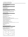
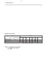
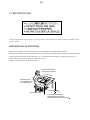
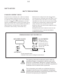
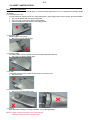
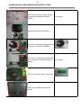
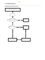
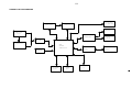
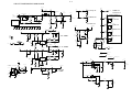
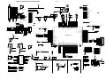
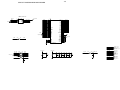
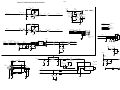
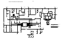
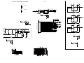
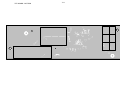
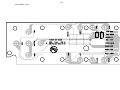
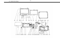
DVD Portable
PD7030/12/51/55/98/77/93/94
Service Manual
TABLE OF CONTENTS
Chapter
Technical Specification, PCBs Location………………….. 1
Safety Instruction ……………………………………………… 2
Instruction for Use……………………………………………… 3
Mechanical and Dismantling Instructions…………………. 4
Service Modes, Troubleshooting……………………………. 5
Overall Block Diagram, Wiring Diagram……………………. 6
Electrical Diagram……………………………………………… 7
Exploded View Diagram & Service Part List………………..8
Revision List……………………………………………………. 9
Copyright 2011 Philips Consumer Electronics B.V. Eindhoven, The Netherlands
All rights reserved. No part of this publication may by reproduced, stored in a retrieval system or
transmitted, in any form or by any means, electronics, mechanical, photocopying, or otherwise
without the prior permission of Philips.
Published by BG AVM
Version
Printed in the Netherlands
1.5
Subject to modification 3142 785 35900
1-1
1.0 TECHNICAL SPECIFICATION
VIDEO/ AUDIO Characteristic Testing discs
Test discs DOLBY: Dolby Test disc
ABEX: TDV-540A
Video (PAL / NTSC)
White bar : 714mV +10%/-20%
Sync. Amplitude: 286mV ±40mV
Burst/chroma ratio: ± 15%
S/N luminance: >42 dB
POWER CONSUMPTION
Power-Supply(AC-DC Adaptor):
Supply voltage: AC 100~240V ±10%
Supply Power consumption(AC adaptor 100/240V): 9V 0.8A +10%
DC Power supply(Operate voltage range): 6.3V-15.49V±10%
Standby Power (AC adaptor, no load),264VAC: <0.75W
GENERAL DESCRIPTION
7" TFT portable DVD player
Key Components: N/A
Optical Pickup: Sanyo 870PH
Loader:ASA PM2371-D/FORYOU DM520
Solution: MTK MT1389Q-DE
Disc Size: 12/8cm
Regional code: region 2 ,/12 version
Playable disc type: DVDRW/DVDR/CD/CD-R/CD-RW
Video format: DVD / SVCD / JPEG / MPEG4 / DIVX3, 4,5,6(Home theater)
Video output signal: PAL /NTSC
Audio format: CD / MP3(32 - 320 kbps)
Video DAC: 10 bit / 54 MHz
Audio D/A converter: 96KHz / 24-bit
User Interface: Philips GUI same as PET745
OSD language: English/French /Germany/Spanish/ Italian for /00, /05 version.
Screen Saver function: Yes
Button functions: Refer to MUS
SD/MMC slot:N/A
USB:YES
DVD PORTABLE PANEL ACCEPTANCE
DVD Portable panel acceptance
/37/17 region: 0 bright dot, 2 color dot, 3 dead dot
Other region: 1 bright, 2 color dot, 3 dead dot
Distance between dot >= 2cm
No bright dot is permitted for A-zone
1-2
1.1 PCBs Location
VERSION VARIATIONS
Type/Versions:
Service policy
Board in used:
MAIN BOARD
KEY BOARD
TFT BOARD
PD7030
12
*TIPS: C -- Component Lever Repair.
M -- Module Lever Repair
X -- OCX
C
M
M
51
C
M
M
55
98
77
94
C
M
M
C
M
M
C
M
M
C
M
M
1-3
1.2 SW upgrade Procedure
Procedure for SW upgrade
1. unzip the .bin file from RAR package
2. copy the file in a CD-ROM or USB
3. read the CD-ROM or USB, followed the display tips, press "OK" key to start the upgrade
PS:
Write the file to a CD-ROM like the way to create a data disc:
1, make sure your PC has disc recorder
2, draw the file to DVD/CD RAM
3, your PC might show the tip to insert a disc to the DVD/CD RAM, then pls insert a CDROM
4, click the "write" to start the copy process
Warning: Do not unplug the AC adapter during firmware upgrade to prevent flash corrupt of the set!!
Procedure to check SW version of your DVD Portable
1.
2.
3.
4.
5.
OPEN
Press SETUP MENU
Select Preferences
Select Version Info
Press “OK” key
2-1
2.0 SAFTETY INSTRUCTIONS
GB
NL
ESD
WARNING
Alle IC’s en vele andere halfgeleiders zijn
gevoelig voor electrostatische ontladingen
(ESD).
Onzorgvuldig behandelen tijdens reparatie kan
de levensduur drastisch doen verminderen.
Zorg ervoor dat u tijdens reparatie via een
polsband met weerstand verbonden bent met
hetzelfde potentiaal als de massa van het
apparaat.
Houd componenten en hulpmiddelen ook op
ditzelfde potentiaal.
All ICs and many other semi-conductors are
susceptible to electrostatic discharges (ESD).
Careless handling during repair can reduce life
drastically.
When repairing, make sure that you are
connected with the same potential as the mass
of the set via a wrist wrap with resistance.
Keep components and tools also at this
potential.
F
WAARSCHUWING
ATTENTION
I
Tous les IC et beaucoup d’autres
semi-conducteurs sont sensibles aux
décharges statiques (ESD).
Leur longévité pourrait être considérablement
écourtée par le fait qu’aucune précaution n’est
prise à leur manipulation.
Lors de réparations, s’assurer de bien être relié
au même potentiel que la masse de l’appareil et
enfiler le bracelet serti d’une résistance de
sécurité.
Veiller à ce que les composants ainsi que les
outils que l’on utilise soient également à ce
potentiel.
D
AVVERTIMENTO
WARNUNG
Alle ICs und viele andere Halbleiter sind
empfindlich gegenüber elektrostatischen
Entladungen (ESD).
Unsorgfältige Behandlung im Reparaturfall kan
die Lebensdauer drastisch reduzieren.
Veranlassen Sie, dass Sie im Reparaturfall über
ein Pulsarmband mit Widerstand verbunden
sind mit dem gleichen Potential wie die Masse
des Gerätes.
Bauteile und Hilfsmittel auch auf dieses gleiche
Potential halten.
Tutti IC e parecchi semi-conduttori sono
sensibili alle scariche statiche (ESD).
La loro longevità potrebbe essere fortemente
ridatta in caso di non osservazione della più
grande cauzione alla loro manipolazione.
Durante le riparazioni occorre quindi essere
collegato allo stesso potenziale che quello della
massa dell’apparecchio tramite un braccialetto
a resistenza.
Assicurarsi che i componenti e anche gli utensili
con quali si lavora siano anche a questo
potenziale.
GB
Safety regulations require that the set be restored to its original
condition and that parts which are identical with those specified,
be used.
“Pour votre sécurité, ces documents
doivent être utilisés par des spécialistes agréés, seuls habilités à réparer
votre appareil en panne”.
NL
Veiligheidsbepalingen vereisen, dat het apparaat bij reparatie in
zijn oorspronkelijke toestand wordt teruggebracht en dat onderdelen,
identiek aan de gespecificeerde, worden toegepast.
CLASS 1
LASER PRODUCT
3122 110 03420
F
Les normes de sécurité exigent que l’appareil soit remis à l’état
d’origine et que soient utiliséés les piéces de rechange identiques
à celles spécifiées.
GB
Warning !
Invisible laser radiation when open.
Avoid direct exposure to beam.
D
Bei jeder Reparatur sind die geltenden Sicherheitsvorschriften zu
beachten. Der Original zustand des Geräts darf nicht verändert werden;
für Reparaturen sind Original-Ersatzteile zu verwenden.
S
Varning !
Osynlig laserstrålning när apparaten är öppnad och spärren
är urkopplad. Betrakta ej strålen.
SF Varoitus !
I
Le norme di sicurezza esigono che l’apparecchio venga rimesso
nelle condizioni originali e che siano utilizzati i pezzi di ricambio
identici a quelli specificati.
Avatussa laitteessa ja suojalukituksen ohitettaessa olet alttiina
näkymättömälle laserisäteilylle. Älä katso säteeseen!
DK Advarse !
"After servicing and before returning set to customer perform a
leakage current measurement test from all exposed metal parts to
earth ground to assure no shock hazard exist. The leakage current
must not exceed 0.5mA."
Usynlig laserstråling ved åbning når sikkerhedsafbrydere er
ude af funktion. Undgå udsaettelse for stråling.
Caution: These servicing instructions are for use by qualified service personnel only.
To reduce the risk of electric shock do not perform any servicing other than that contained in the operating instructions unless you are qualified to do so.
2-2
2.1 ESD PROTECTION
Whenthepowersupplyisbeingturnedon,youmaynotremovethislasercautionslabel.Ifitremoves,radiationoflaser
maybereceived.
PREPARATIONOFSERVICING
PickupHeadconsistsofalaserdiodethatisverysusceptibletoexternalstaticelectrocity.
Althoughitoperatesproperlyafterreplacement,ifitwassubjecttoelectrostaticdischargeduringreplacement,
itslifemightbeshortened.Whenreplacing,useaconductivemat,solderingironwithgroundwire,etc.to
protectthelaserdiodeformdamagebystaticelectricity.
Andalso,theLSIandICaresameasabove.
Groundconductive
wriststrapforbody.
Solderingiron
withgroundwire
orceramictype
1M
Conductivemat
Thegroundresistance
betweenthegroundline
andthegroundislessthan10
2-3
SAFTY NOTICE
SAFTY PRECAUTIONS
LEAKAGE CURRENT CHECK
Plug the AC line cord directly into a 120V AC outlet (do
Measure the AC voltage across the 1500
not use an isolation transformer for this check). Use an
AC voltmeter, having 5000 per volt or more sensitivity.
The test must be conducted with the AC switch on and
then repeated with the AC switch off. The AC voltage
Connect a 1500
indicated by the meter may not exceed 0.3V.A reading
10W resistor,paralleled by a 0.15uF
resistor.
150V AC capacitor between a knomn good earth ground
(water pipe, conduit, etc.) and all exposed metal parts of
exceeding 0.3V indicates that a dangerous potential
exists, the fault must be located and corrected.
cabinet (antennas, handle bracket, metal cabinet
screwheads, metal overlays, control shafts, etc.).
Repeat the above test with the DVD VIDEO PLAYER
power plug reversed.
NEVER RETURN A DVD VIDEO PLAYER TO THE
CUSTOMER WITHOUT TAKING NECESSARY
CORRECTIVE ACTION.
READING SHOULD NOT EXCEED 0.3V
AC VOLTMETER
DVD VIDEO PLAYER
(5000 per volt
or more sensitivity)
1500
10W
AC OUTLET
Good earth ground
such as a water pipe,
conduit, etc.
0.15uF 150V AC
Test all exposed metal.
Voltmeter Hook-up for Leakage Current Check
The lightning flash with arrowhead symbol, within an
equilateral triangle, is intended to alert the user to the
presence of uninsulated "dangerous voltage" within the
product's enclosure that may be of sufficient magnitude to
constitute a risk of electric shock to persons.
The exclamation point within an equilateral triangle is
intended to alert the user to the presence of important
operating and maintenance (servicing) instructions in the
literature accompanying the appliance.
2-4
2.2 SAFETY INSTRUCTIONS
Battery Handling Guideline
Since the battery is packed in soft package, to ensure its better performance, it’s very important to carefully handle
the battery
2.2.1 Soft Aluminium foil
The soft aluminum packing foil is very easily damaged by sharp edge parts such as Ni-tabs, pins and needles.
• Don’t strike battery with any sharp edge parts
• Trim your nail or wear glove before taking battery
• Clean worktable to make sure no any sharp particle
2.2.2 Sealed edge
Sealing edge is very flimsy
• Don’t bend or fold sealing edge
2.2.3 Folding edge
The folding edge is form in battery process and passed all hermetic test.
• Don’t open or deform folding edge
2.2.4 Tabs
The battery tabs are not so stubborn especially for aluminum tab.
• Don’t bend tab
2.2.5 Mechanical shock
• Don’t Fall, hit, bend battery body
2.2.6 Short
Short terminals of battery is strictly prohibited, it may damage battery.
Caution: Danger of explosion if battery is incorrectly replaced.
Replace only with the same or equivalent type.
3-1
3.0 Instruction for Use
You can download this information from the following websites:
http://www.philips.com/support
http://www.p4c.philips.com
4-1
4.0 MECHANICAL AND DISMANTLING INSTRUCTIONS
Remove nine screws on back cabinet
to separate top cabinet and back
cabinet.
screws 9pcs
Generally open the front cabinet.
Remove 3 screws and disassemble the
connecter on the DVD LOADER.
Remove four screws and disassemble
the connecter on the Main board and screws 4pcs.
Battery.
Remove six screws on the key board.
Remove the speaker grill and 4pcs
screws. .
5-1
5.0 TROUBLESHOOTING
SYMPTOM: NO IMAGE / NO SOUND
SYMPTOM: NO IMAGE OUTPUT( THE PANEL SHOW BLUE PICTURE
)
Start
Check DVD Drive work?
no
Replace DVD Drive
no
Exchange AV cable
yes
NOTE: AV Cable TYPE from outside to
Inside L-Audio, R-Audio, Video, Ground
Check the external AV
Cable TYPEnote and
connection is OK?
yes
Replace Main Board
SYMPTOM: NO SOUND COMES FROM SPEAKER
Start
Check the Connection OK?
no
Reinsertion
no
Change the speaker
yes
Check speaker OK?
yes
Replace Main Board
5-2
5.0 TROUBLESHOOTING
SYMPTOM: THE DVD DRIVE DOES NOT WORK
SYMPTOM: THE DVD DRIVE DOESN
ϗT WORK
Start
Check DVD-Loader
connection OK?
NO
Cable Reinsertion
NO
Replace DVDLoader
Yes
Check the DVD-Loader
OK?
Yes
Replace main board
5-3
5.0 TROUBLESHOOTING
SYMPTOM: ADAPTOR CANNOT POWER ON
Adaptor can not Power ON
Start
Check Adaptor OK?
NO
Change adaptor
SET OK?
Yes
Yes
No
Check the Power-ON
button and cable OK?
YES
Return set to
Customer
Replace Main Board
NO
Replace Button or
Cable
OK
5-4
5.0 TROUBLESHOOTING
SYMPTOM: LED DISPLAY FAILURE
SYMPTOM: LED Display Fail
Start
Check CABLE form Main board to top board
connection OK?
NO
Cable Reinsertion
Yes
Check TOP-board OK?
NO
Replace LED
NO
Replace top board
OK
Yes
OK
Replace main board
OK
Return to custormer
5-5
5.0 TROUBLESHOOTING
SYMPTOM: KEY & BOTTON FAILURE
SYMPTOM: Key & Botton Fail
Start
Check CABLE form board to
board connection OK?
NO
Cable Reinsertion
Yes
Check KEY board OK?
NO
OK
Yes
Replace main board
Replace KEY board
OK
Return to custormer
6-1
OVERALL BLOCK DIAGRAM
AV OUT JACK
L/R AND CVBS
TFT PANNEL
Hannstar/ CPT
BACK LIGHT
EARPHONE
Power input
9~15V
AMPLIFIER
SPEAKER
0.2W X2
DC-DC
PolymerBattery
MPEG
DECODER
MOTOR DRIVER
SPHE8202PS-A
KEY
CONTROL
SW5888
SPI FLASH
16M/8M
SDRAM
4X16
USB
2.0
LOADER(SANYO
SP850)
7-1
CIRCUIT DIAGRAM-DVD MAIN BOARD
BAT_OUT
BAT_OUT
DIS-CHARGE
4
1
L-851
D1
SS14
DVCC3
D2
15V
560R/NC
R45
4.7K/NC
Q1
SI2307
R2
100K
ON/OFF
3
GND
3
Q2
1
ADAPTER_DET
2
R5
6.8K
1
2N3904
2
SPI Flash +3.3V
Close to 8202P-A
RFGND
M+5V
L4
C69
0.1uF/25V(NC)
Servo MOTOR +5V
100uH
L5
C4
PGND
DGND
MGND
SGND
PGND
ADGND VGND CARDGND GND
RFGND
Video buffer +5V
DC_IN
D3
FB600R/2A
Q4 SI2307
2
3
C10
0.1uF/25V
MARK1
MARK2
MARK3
MARK4
R6
10
R254
22K
2
S
L9
C9
+
18K
R9
10K
CE
U1
SS7701
+5V POWER
VFB
R10
R12
10K
2.7K
L33
FB600R/2A
R255
NC
C19
R13
10
R257
22K
0.1uF/25V
2
1
5
5
6
6
R133
47K
EC13
DVCC_3.3V
PGND
L2
GND
FB120R
SPI_VCC3
DVCC3
D28
3.6V
560R
R15
22K
C24
1000pF
3
R16
2.7K
C20
1
1000P
2
VFB
DVCC3 3,6
B-CHARG
B-CHARG 5
ADAPTER_DET
R17
10K
PS
Q42
NC/2N3906
U3
UTC1117-ADJ
IN
OUT
D18
BAT54S
2
1
2
R18
C25
100uF_10V
100nF
1K
GND
3
2
R258
1
Q43
1$$$16 2N3906
4.7k
C119
1uF/50V
ADAPTER_DET 3
VGL
1
2
R58
EC14
R240
100R
1
PLL_VDD1.2
VCC1.2
2
2
3
C116 100nF/25V
1
2
3
D19
C118 100nF/25V BAT54S
1
2
3
C120
1uF/50V
NC
PGND
PGND
GND
PGND
PGND
D21
2
BAT54S
2
VGH
VGH
1
1K
C122
C81
1uF/50V
1
R241
1k
R242
C123
2
0.01uF/50V
1uF/50V
2
DC_IN
ZD7
16V
PGND
1
GND
1
PGND
1
C121 100nF/25V
1
2
3
2
R134
27R
VGL
EC48
10uF_16V
PGND
DVCC3
+1.25V
POWER
VGL
ZD6
6.8V
CHARGE_STAR
POWER_SWITCH_SK-22D13-V4
PGND
C23
4
DVCC3
B-CHARG
GND
1
关
4
DVCC_3.3CORE
FB120R
2
1
4
2N3904
C11
100uF_10V 100nF
C18
100nF
R14
1
2
G
3
G
3
L6
8
ON/OFF
7
开
+3.3V POWER
DVCC3
DVCC3
GND
D25
NC/3.0V
DC9V_IN
CE
U2
SS7701
GND EXT
1
R256
NC
PGND
POWER ON
VIN
2
5
C21
1uF/25V
CHARGE_STOP
NC/47K
SW1 R249
EC7
2
1K
220uF/16V
PGND
R253
0R
EC11
+
PS
1
+
AVCC3
100nF 47uF_16V
L12
47uH
EC10
AUDIO DAC +3.3V
3.3uH_0805
2N3904
Q23
2
Q22
1
D5
SS24
100uF/25V
R20
R7
PGND
Q5 SI2307
2
3
POWER Switch
1000pF
2
C8
GND
3
22K
C12
1
DC_IN
POWER
OFF
B-CHARG
15V
1
PGND
3
EC4
2
1
1uF/25V
GND EXT
VIN
Q21
SI2307
VIDEO DAC +3.3V
VVCC3
3.3uH_0805
47K
D14
4
R11
5
C15
L8
220uF_10V 100nF
1
2
PGND
D4
0.1uF/25V
R132
3
P+5V
C22
R130
47K
GND
D3
G
R131
1.5K
EC5 100nF
220uF/16V
R8
电源指示green
C7
100uF_10V 100nF
PGND
P+5V
1
+
USB +3.3V
EC3
CHARGE_IN
SS24
47uH
EC6
USB_AVDD3V3
2.2R
TGND
L31
100uF/25V
RF +3.3V
RFGND
Q3
2N3904
1
AGND
PGND
C5
100uF_10V 100nF
L7
PGND
RF3.3V
EC2
100nF
DC9V_IN
RFGND
FB120R
21
R260
SDRAM +3.3V
100nF
DC_IN
D3
G
H=PLUG_IN
L=PLUG_OUT
2
S
R4
100K
FB120R
SD_VCC3
2
X00223
C3
0.1uF/25V
VDS=30V
VGS=20V
Current=8A
PGND
R3
10K
L1
C1
1
C2
0.1uF/25V
DC/JACK
DC9V_IN
3
2
D8
SS24
Servo analog +5V
2.2_0805
2
P
3
2
L3
NC
R1
1
1
DC
INPUT
6~15V
F1
PolyFuse/8v/0.75A
C16
0.1uF/25V(NC)
DVCC3
A+5V
P+5V
1
CN1
9V_IN
D7
SS24
PGND
7-2
GND
R32
XT1
USB 2.0
C72
GND
NC
GND
GND
10
FB120R
DA_VDD
C124
0.1uF
9
GND
C37
C38
RFGND
C39
RFGND
C40
DVDVR
CDVR
ADAPTERDET
SPI_CE
SPI_D0
SPI_CLK
SPI_D1
C41
0.1uF
DVCC_3.3V
RFGND
R179
DVCC_3.3V
DVCC3
10K RESET_DEMOD
R43
C49
C50
M+5V
C46
EC22
C47
470uF_6.3V 0.1uF 0.1uF
RFGND
DVCC_3.3CORE
GND
VINFC
CFCerr1
CFCerr2
VINSP
VNFFC
FWD
REV
STBY
BIAS
VINTK
CTKerr1
CTKerr2
VINSL
PreGND
28
27
26
25
24
23
22
DMEA
VREF2 C45
TCO
RFGND
0.1uF
GND2
GND1
29
RFGND
8
9
10
11
12
13
14
Vcc1
VOLDVOLD+
VOSPVOSP+
VOFCVOFC+
VCTL
VNFTK
Vcc2
VOSLVOSL+
VOTKVOTK+
21
20
19
18
17
16
15
M+5V
FOCFOC+
$$$14
SLED+
SLEDRADRAD+
1
2
CN4
2P/2.0
SPSP+
HOME
R_FGND
SLEDSLED+
SPSP+
HOME
R_FGND
C52
C53
C54
C55
C56
C57
0.1uF
0.1uF
0.1uF
0.1uF
0.1uF
0.1uF
0.1uF
GND
EC23
10uF_16V
SLEDSLED+
TP69
TP70
TP71
TP72
TP73
TP74
RF3.3V
C51
R49
RFGND
GND
VCC
DET
C130
C131
C132
C133
C134
C135
C136
C137
C138
C139
100pF
100pF
100pF
100pF
100pF
100pF
100pF
100pF
100pF
100pF
B/U
G/Y
R/V
P_STHL
P_OEH
P_OEV
P_CKV
P_STVU
DC_COM
AC_COM
B/U
G/Y
R/V
P_CPH1
P_STHL
P_OEH
P_OEV
P_CKV
P_STVU
GND
DC_COM
AC_COM
GND
这几个改1000P?
GND
FB17
FB18
FB19
FB20
FB600R
FB600R
NC
NC
SDA
SCL
UA_TX
UA_RX
GND
RFGND
UART/I2C
The Cover Limit Switch
C13
0.1uF BACKL_E
C152
0.1uF DVCC3
C153
0.1uF P_+5V
C140
1000pF
VGH
C141
1000pF
VGL
C142
1000pF
J7
P_PWM2
DVCC_3.3V
4P/2.0
4
3
2
1
PLL_VDD1.2
RESET
SW5888 HSOP28
CN3
VCC1.2
GND
30
1
FB120R
0.1uF
M+5V
SP-
R24
GND
C48
SCO
RFGND
R44
SP+
XOPVIP
XOPVIN
SPDCO
1
2
3
4
5
6
7
P_CPH1
0.1uF
U5
FCO
0.1uF
R50
10K
D6
1N4148
RESET_B
Q11
2N3904
4
2
DISC_SWITCH_TC-0030
1 R48
10K
SW3
R47
10K
100
DVCC3
3
TP10
Reset
GND
FB9
R46
FB600RCOVER_SW
0.1uF
C150
CN5
UA_TX
UA_RX
1000pF
GND
GND
TP11
TP12
DVCC_3.3V
P+5V
C58
4.7K
SDA
SCL
1
2
3
4
1
2
3
4
NC/CON4/1.25MM/DIP
GND
P_STVU
P_CKV
P_OEV
P_OEH
P_STHL
TP48
TP49
TP50
TP51
TP52
TP53
TP54
TP55
TP56
TP57
TP58
TP59
TP60
P+5V
RFGND
FB600R
FB600R
FB600R
FB600R
FB600R
DVCC3
RFGND
FB3
FB4
FB5
FB6
FB7
C146
NC/1000pF SDA
C147
NC/1000pF SCL
8
7
6
5
4
3
2
1
8
7
6
5
4
3
2
1
L30
FB600R/2A
P_+5V
PUH_DVDLD
STVU
CKV
OEV
OEH
STHL
GND
GND
D24
1N4148(NC)
J6
CON14/1.25mm/DIP
1
2
3
4
5
6
7
8
GND
9
10
11
12
13
14
AC_COM
DC_COM
BACKL_E
P_PWM2
GND
R245
FB600RBACKL_EN
FB8
FB600RPWM2
8pin/1.25w
TP61
TP62
TP63
TP64
TP65
TP66
TP67
TP68
D23
1N4148(NC)
GND
10uF_16V
U4
DVCC_3.3CORE
Q10
S8550
EC17
M_A3
M_A2
M_A1
M_A0
M_A10
M_BA1
M_BA0
M_RAS
M_CAS
M_WE
M_DQM0
M_A4
M_A5
M_A6
M_A7
M_A8
M_A9
M_A11
M_CLK
RFGND
3
PUH_CDLD
3
Q9
S8550
2
GND
0.1uF
DVDLDO
2
RFGND
C42
0.1uF
R/V
G/Y
B/U
5
RFGND
VREF1
EC19
10uF_16V
C36
AVCC3
DAC_VREF
PWM2
10
47uF_16V
SCL 5
GND
AC_COM
AOUT_R
AOUT_L
64
63
62
61
60
59
58
57
56
55
54
53
52
51
50
49
48
47
46
45
44
43
42
41
40
39
BATSDA 5
SCL
C151
NC/1000pF
5
0.1uF
CDLDO
EC21
GND6
GND7
GND8
GND9
RESET_DEMOD
RFGND
R42
5.1
C44
47uF_16V
1N17016202
0.1uF
EC20
1N17016190
R41
5.1
143
129
130
131
132
133
134
135
136
137
140
141
RF3.3V
C43
10K
RF3.3V
ADAPTER_DET 2
SDA
TCON_AC_VCOM
AOUT_R
AOUT_L
ADAC_AVDD
VREF
AUDIO_MUTE/GPIO54/HSYNC(3)
SPDIF_OUT/GPIO53/VSYNC(3)
M_A3
M_A2
M_A1
M_A0
M_A10
M_BA1
M_BA0
M_RAS
M_CAS
M_WE
M_DQM0
M_A4
M_A5
M_A6
M_A7
M_A8
M_A9
M_A11
M_CLK
SPHE8202PS-A
DVCC_3.3CORE
EC18
10uF_16V
TP9
FGIN
R244
470R/0R VREF_2
OPVIP
OPVIN
DVDLDO
CDLDO
MDI
SRV_AVDD
V21
V165
VDDQ
DA_TEO
DA_FEO
DA_AVDD
SPDC_OUT
SC_OUT
DMEA
FGIN
DVDVR/SCL/GPIO74
CDVR/SDA/GPIO75
CARD_SENSE/GPIO80
SPI_CE
SPI_D0
SPI_CLK
SPI_D1
SD_D0/MS_D0
SD_CLK/MS_CLK
SD_CMD/MS_BS
GND5
FB10
NC/FB600R ADAPTER_DET
ADAPTERDET
10
GND
VREF1
VREF_2
OTP
DA_TEO
DA_FEO
DA_VDD
SPDC_OUT
SC_OUT
0
GND R36
680pF
TCO
R37
91K
1000pF FCO
R38
20K
DA_VDD
0.1uF SPDCO
R39
2.2K
SCO
R40
2.2K
0.1uF DMEA
FB11
FB600R
103
104
105
106
107
108
109
110
111
112
113
114
115
116
117
118
119
120
121
122
123
124
125
126
127
128
142
DVCC3 2,6
9
C129
RF3.3V
TP47
CLOSE TO 8202
VREF2
XOPVIP
XOPVIN
DVDLDO
CDLDO
DVDMDI
SPI_D0 4
SPI_D1 4
SPI_CE 4
SPI_CLK 4
DVCC3
1
2
3
4
5
6
7
8
9
10
11
12
13
14
15
16
17
18
19
20
21
22
23
24
25
26
27
28
29
30
31
32
33
34
35
36
37
38
R243
91K/NC
L29
DVCC_3.3V
GND10
GND11
GND12
GND13
GND14
GND15
GND3
GND4
RF3.3V
C128
1N4148
8
7
6
5
4
3
2
1
RFGND
1000pF
D17
C127
1N4148
1000pF
D16
1000pF
1N4148
1000pF
D15
C126
R178
R177
R176
FB600R
FB600R
FB600R
FB600R
R175
FB12
FB13
FB14
FB15
KOUT1
KOUT2
KOUT3
SPI_D0
SPI_D1
SPI_CE
SPI_CLK
9
TP40
TP41
TP42
TP43
TP44
TP45
TP46
10K
10K
10K
10K
C78
U17
KEY0
KEY1
KEY2
KEY3
27MHz
EC16
10uF_16V
RF3.3V
DVCC3
J5
8PIN/1.25L
C33 10pF
15
NC
4.7K
16
C6
100uF/10V
2
C29 100pF
4
3
2
1
VGL
FUSE(5V600MA)
GND
C80
M_A11 4
M_CAS 4
M_RAS 4
M_WE 4
M_BA0 4
M_BA1 4
M_CLK 4
VGH
+ EC8
0.1uF
$$$3
$$$4
$$$2
M_A11
M_CAS
M_RAS
M_WE
M_BA0
M_BA1
M_CLK
6
RFGND
C75
0R
0R
M_A[0..11] 4
M_D[0..15] 4
M_DQM[0..1] 4
139 MARK2
SANYO
850/870
Hitachi 1200X
L10
P+5V
R61
R60
AOUT_R 6
AOUT_L 6
GND
C14
1000pF
6
1000pF
USB_DP
USB_DM
B/U
G/Y
R/V
150
150
150
COVER_SW
IR_IN
M_D0
M_D1
M_D2
M_D3
M_D4
M_D5
M_D6
M_D7
M_D15
M_D14
M_D13
M_D12
M_D11
M_D10
M_D9
M_D8
M_DQM1
C125
0.1uF
PUH_DVDLD
GND
CN9
GND
KEY0
KEY1
KEY2
KEY3
10uH
TP19
TP20
TP21
TP22
TP23
TP24
TP25
TP26
TP27
TP28
TP29
TP30
TP31
TP32
TP33
TP34
TP35
TP36
TP37
TP38
TP39
FB600
VCC1.2
200R
L14
C145
1000pF
GND
R174
RESET_B
BACKL_EN
R129
PUH_DVDLD#
A+5V
IR_IN
R28
R31
R34
CVBS 6
AOUT_R
AOUT_L
138 MARK1
close to 8202p
R26 FB600R CD_VR
FB600R DVD_VR
PUH_CDLD
10uH
HOME
GND
GND
GND
E
102
F
101
A
100
B
99
C
98
D
97
C30 33pF
PUHRF
96
C35
1uF
95
LDSW
94 FB21
GND
FB600R HOME
93
CLKOUT
92 FB600R FB16
CLKIN
91
C31 33pF
90
PLL_VDD1.2
USB_DM
89
USB_DP
88
87
USB_AVDD3V3
C32 2200pF
COMP
86
GND
R35
10K
85
84
DVCC_3.3CORE
83
FB1000R(SZ1005K102)
82
R30
CPH1
P_CPH1
81
STHL
80
OEH
79
78
VCC1.2
OEV
77
CKV
76
GND
GND
STVU
75
74
DVCC_3.3CORE
B/U
73
G/Y
72
R/V
71
70
69
VVCC3
CVBS
68
V_FSADJ
R33
1K
67
GND
V_COMP
66
DC_COM
65
VVCC3
RFGND
R27
L13
C34
FOCFOC+
RAD+
RADC
D
/LDSW
PUHRF
A
B
F
VREF1
E
CDVR#
DVDVR#
PUH_CDLD#
DVDMDI
PUH_DVDLD#
A+5V
RFGND
A_+5V
4.7K
CDVR
DVDVR
100nF
CVBS
CDE
CDF
DVDA
DVDB
DVDC
DVDD
RFIS
AD_AVDD
LDSW
HOME/CARD_RST
CLKOUT
CLKIN
PLL_VDD12
USB_DM
USB_DP
USB_AVDD
COMP
FB
DCDC_PWM
DCDC_VCC3
TCON_PWM
TCON_CPH1
TCON_STHL
TCON_OEH
VDD12
TCON_OEV
TCON_CKV
TCON_STVU
VDD_33
TV_DAC3
TV_DAC2
TV_DAC1
TV_AVDD
TV_AVDD
TV_DAC0
V_FSADJ
VCOMP
TCON_DC_VCOM
0.1uF
0.1uF
0.1uF
CD_VR
DVD_VR
R29
RF3.3V
C114
EC47
10uF_10V
5
6
C27
C28
C74
P+5V
LDSW
IR(NC)
RESET_DEMOD
TS_ERR
VDD_33
RESET_B
TS_SYNC
TS_DATA
TS_DEN
TS_CLK
VDD12
GPIO7/HSYNC(1)
GPIO8/VSYNC(1)
GPIO9
GPIO10
GPIO11
GPIO12
GPIO13
GPIO14
GPIO15
GPIO16
IR/GPIO17
M_D0
M_D1
M_D2
M_D3
M_D4
M_D5
M_D6
M_D7
M_D15
M_D14
M_D13
M_D12
M_D11
M_D10
M_D9
M_D8
M_DQM1
VDD_33
26
close to connector
CDVR#
DVDVR#
PUH_CDLD#
DVDMDI
A_+5V
RFGND
/LDSW
RFGND
VREF1
RFGND
R19
10K
100uF_10V 0.1uF
E
CN2
C26
EC15
FOCFOC+
RAD+
RADC
D
/LDSW
PUHRF
A
B
F
U16
7
8
25
A+5V
1
2
3
4
5
6
7
8
9
10
11
12
13
14
15
16
17
18
19
20
21
22
23
24
A+5V
3
A+5V
RFGND
1
CIRCUIT DIAGRAM-DVD MAIN BOARD
GND
7-3
CIRCUIT DIAGRAM-DVD MAIN BOARD
U6
EON25T16/MX25L1605
SPI_CE
DQ0
SPI_WP
1
2
3
4
GND
8
7
6
5
VCC
/CS
DO /HOLD
CLK
/WP
DIO
VSS
SPI_HOLD
SPI_CLK_1
DQ1
SPI_VCC3
M_A0
M_A1
M_A2
M_A3
M_A4
M_A5
M_A6
M_A7
M_A8
M_A9
M_A10
M_A11
M_DQM0
M_DQM1
M_WE
M_CAS
M_RAS
23
24
25
26
29
30
31
32
33
34
22
35
15
39
16
17
18
19
GND
SD_VCC3
DQ0
R51
NC
RAM_CLK
M_BA0
M_BA1
DQ1
U8
A0
A1
A2
A3
A4
A5
A6
A7
A8
A9
A10/AP
A11
LDQM
UDQM
WE
CAS
RAS
CS
37
38
20
21
CKE
CLK
BA0
BA1
6
12
46
52
VSSq
VSSq
VSSq
VSSq
GND
D0
D1
D2
D3
D4
D5
D6
D7
D8
D9
D10
D11
D12
D13
D14
D15
NC
NC/RFU
2
4
5
7
8
10
11
13
42
44
45
47
48
50
51
53
36
40
VSS
VSS
VSS
VDD
VDD
VDD
VDDq
VDDq
VDDq
VDDq
28
41
54
1
14
27
3
9
43
49
M_D0
M_D1
M_D2
M_D3
M_D4
M_D5
M_D6
M_D7
M_D8
M_D9
M_D10
M_D11
M_D12
M_D13
M_D14
M_D15
GND
SD_VCC3
SDRAM_1Mx16x4
M_A[0..11] 3
M_D[0..15] 3
M_DQM[0..1] 3
SPI_VCC3
SPI_D0
SPI_D1
SPI_VCC3
SPI_CLK
R52
R54
0R
0R
DQ0
DQ1
R55
R56
10K
10K
SPI_WP
SPI_HOLD
R57
33R
SPI_CLK_1
C68
NC
GND
SD_VCC3
M_CLK
EC24
C59
10uF_16V 100nF
GND
EC25
C60
C61
C62
C63
C64
C65
C66
100uF_10V 100nF 100nF 100nF 100nF 100nF 100nF 100nF
GND
R53
RAM_CLK
33R
C67
10pF
GND
M_CAS
M_RAS
M_WE
M_BA0
M_BA1
M_CLK
SPI_D0
SPI_D1
SPI_CE
SPI_CLK
M_CAS 3
M_RAS 3
M_WE 3
M_BA0 3
M_BA1 3
M_CLK 3
SPI_D0 3
SPI_D1 3
SPI_CE 3
SPI_CLK 3
7-4
CIRCUIT DIAGRAM-DVD MAIN BOARD
C70
DC_IN
120pF
Q14
SI2307
2
D3
S
10K
5.1K
C73
2
3
1200pF
VREF3
1
EC32
R94
EC34
22uF/25V
R_OUT
360R
U11A 10uF_16V
NJM4558
D27
IN4148
R90
$$$18
R96
2R(0805)
2R(0805)
R95
680K
EC9
AU_OP
GND
9V FOR 2822
G
+
8
10uF_16V
R93
+
R92
-
EC12
AOUT_R
1
4
GND
AU+9V
C17
100pF
10uF_16V
R101
27K
C76
DVCC3
GND
120pF
CVBS
GND
4
C79
6
5
1200pF
VREF3
7
EC37
R110
360R
R_OUT R108
L_OUT R111
L_AMP
R_AMP
L_OUT
U11B 10uF_16V
NJM4558
24K
24K
$$$7
$$$6
5
4
3
2
6
1
7
AU_OP
GND
J8
VR1
C10K F-1001G -3
volume
SPK_R
1
2
3
4
SPK_L
AGND
1
2
3
4
CON4/1.25MM/DIP
EC27 10uF_10V
8
7
6
5
$$$11
$$$10
56K
56K
R118
10K
N16885333 EC38
1
2
3
4
-IN 1_OUT
+IN
VDD
+IN 0_OUT
-IN
GND
N16885345
R119 C85 C86 EC40
EC41
D2822
10K
100pF 100pF 100uF_16V 100uF_16V
GND
EC39
100uF_16V
N16885287
L19
FB2.2K
HP_R
100uF_16V
N16885289
L20
FB2.2K
HP_L
GND
C83
C84
0.1uF
0.1uF
R122
4.7
GND
GND
DC_IN
R123
4.7
TP78
R115
R116
TP77
$$$8
$$$15
U12
TP75
EC1
L_AMP
R_AMP
10uF_10V
TP76
6
AU+9V
AOUT_R 3
AOUT_L 3
5
10K
5.1K
CVBS 3
AOUT_R
AOUT_L
8
10uF_16V
R107
+
R106
-
EC26
AOUT_L
DVCC3 2,3
5
27K
6
R88
AU_OP
L18
FB120R
EC33
C71
22uF_25V0.1uF
GND
AU_OP
GND
10pF
L22
3 CVBS
100nF
2
4
7
HP_L
L R
11
9
10
VGND
R126
180R
GND
VGND
VGND
3
2
C93
VGND
DVCC3
L_OUT
L23 FB2.2K
R_OUT
L24 FB2.2K
100nF
GND
D29
BAT54S(NC)
1
0.1UF 0.1UF
C94
AV_OUT
SPK_L
SPK_R
C92
5
3
1
8
6
J4
Earphone
R127
100K
R128
100K
GND
AGND
VREF3
EC36
100uF/10V
100pF
100R 1%
HP_R
GND
100pF
FB2.2K
4
R125
C89
1uH 0805
N18158338
1
L
2
GND
3
CVBS
5
C91
C88
$$$5
GND
J3
AV_OUTJACK
C77
R109
100uF_10V 47pF
12K
56k
GND
GND
R1
R124
180R
R102
51k
10K
EC42
R2
L21
+
C87
GND
AGND
VGND
7-5
CIRCUIT DIAGRAM-DVD MAIN BOARD
TP79
TP80
Q24
2SB772D
BATTERY
1
5
1K
BATTERY
1
6
0.1uF
DO
VSS
1
4.7M
+
N20879373
C110 C112
0.1uF
0.1uF
SH69P48AM/BQ100
R172
R166
NC
TP85
0.01uF
LED_RED
B+
0.uF
R150
150K_1%
TP86
R151
Vout_DET
GND
R154
GND
R168
R169
0.1R
0.15R
NC
GND
C105
0.1uF
BAT2
2
C102
1
S2
2
D2
8
SCL
1K
C109
G2
BATSDA
C107
D13
NC
GND
B-CHARG 2
100K
BAT_GND
N18018963 R163
Iout_DET
3
B-CHARG
R156
Vout_DET
1K
10K
Q28
9926
SCL
N20881055
N20879818
N20881025
D2
20
19
18
17
16
15
14
13
12
11
S1
NC
D1
PD2
PD1
PD3/PWM1
PD0
PC2/PWM0 PC1/VREF
PC3
OSCO/PC0
RST/VCC
OSC1/SCK
GND
VDD
PA0/AN0
PB3/AN7
PA1/AN1
PB2/AN6
PA2/AN2
PA2/AN5
PA2/AN3
PA2/AN4
TP15
BAT_GND
4
TP84
B-
C104
0.1uF
7
1
2
3
4
5
6
7
8
9
10
PWM1
C103
0.1uF
R167
R165
10K
U14
N17530369
C101
0.47uF
1K
G1
R157
100R
TP83
CHARGE_LED N20876921
R149
CO
6
BATSDA
C100
10uF_16V
R148
P+5V
IN4148
R153
51K_1%
68K
3
1
N17529643
4.7K
R141
VC
BAT1
2
EC46
C97
D26
N20875627
R140
R147
D1
TP82
VM
NC
5
TP81
2
P+5V
N20875945
TVCC
+
4
TP14
Q6
2
3904
1
R144
3.3K
3
R145
3
3
0.1uF
NC
R138
680R
Q27
2
2
ZD5
TL431
N20875929
R139
680R
C99
U13
8242
B-CHARG
GND
$$$13
1
2
1K
NC
R59
C98
1000pF
D22
D12
$$$12
N17854794
TL431
1
3
8/5
D10
100R
5.6V
1000pF
1
N17836826
R136
GND
9013
R143
2K
3904
R137
1
Q26
Q25
2
33uH/2A
+
SS14
0.1uF/25V
47uF/25V
3 N17529601
1K
N17529623
2
$$$40
IN4148
TP13
BAT_OUT
VCC
3
D9
+
R142
R135
10R
2
C95
EC45
D11
IN4148
BAT_OUT
BAT_OUT
$$$1
3
C96 1uF/50V
1
B+
L27
220uF/16V
CHARGE_IN
GND
TP1
BATSDA 3
SCL 3
7-6
CIRCUIT DIAGRAM-TFT BOARD
PVB_5V
PANEL_VGL
-10V
R89
R90
3.9K
390
PVB_BIAS
R91
C71
0.1uF
10K
BC15
2.2uF_16V
P_R/V
BC18
10uF_10V
2
Q14
2N3904
1
10uF_10V
P_GND
VCOM_5V
PANEL_VGH
+15V
R58
C9
2.2uF/25V
P_AC_COM
10K
R62
EC26
10uF_10V
R59
4.7K
P_GND
R65
20K
R67
0R
P_GND
PANEL_VGL
R63
20K
R64
10K
U9
1
2
3
4
O/P_A
-I/P_A
+I/P_A
GND
P_P+5V
27K
YD3414
V+
O/P_B
-I/P_B
+I/P_B
8
7
6
5
R60
100K
R61
10K
R98
PANEL_VGL
R99
100
1k
P_DC_COM
PANEL_VCOM
EC27
10uF_10V
P_GND
R104
NC
VCOM
VCOM_5V
R71
R/V_P
3
C11
PVB_5V
PVB_BIAS
2.2R
BC4
BC5
10uF_10V 100nF
R92
R93
3.9K
390
BC14
R94
C72
10uF_10V 0.1uF
10K
BC16
P_GND
P_G/Y
10uF_10V
2
Q15
2N3904
10uF_10V
1
P_FB
G/Y_P
3
BC19
P_P_PWM
P_GND
EC32
C76
100nF
GND
P_GND
100nF
P_GND
GND
OV
5
4
EN
FB
3
BL_EN
10K
Q17
2N3904
2
P_GND
FB/120R
LED-
C75
100nF
100
R83
R85
510
510
510
510
R74
0
PANEL_VGL
PANEL_VGH
STVU
CKV
R77
U/D
OEV
R78
PANEL_VCOM
R80
L/R
MOD
R81
P_P_OEH
R82
P_P_STHL
R84
NC
10K
10K
NC
10K
NC
P_GND
P_P_CPH1
P_P+5V
P_P+3V3
P_GND
R105
NC
PVB_5V
P_P+5V
P_GND
P_P+5V
P_GND
R95
R96
3.9K
390
PVB_BIAS
R97
C73
0.1uF
10K
BC17
P_P+5V
P_GND
P_B/U
BC20
B/U_P
10uF_10V
2
Q16
2N3904
10uF_10V
P_GND
P_GND
R/V_P
G/Y_P
B/U_P
R102
R103
100
1k
P_PANEL_VAA
P_GND
R106
NC
P_GND
R69
2.2R
R70
7.5R
P_PANEL_VAA
R88
P_GND
PVB_BIAS
10K
PR20
10K
DCDC_5V
P_GND
BC10
EC28
100nF
10UF/10V
P_P+5V
PVB_5V
L18
FB/600R
P_GND
TP66
C70
0.1uF
P_GND
J4
9
10
8
7
9 6
5
4
10 3
2
1
P_P_CPH1
8
7
6
5
4
3
2
1
P_DCDC_PWM
P_FB
P_P_PWM
PWM2
P_P_STHL
P_P_OEH
OEV
CKV
STVU
P_DC_COM
P_AC_COM
8pin/1.25w
P_GND
J1
CON14/1.25mm/DIP
1
2
3
4
5
6
15
7
8
16
9
10
11
12
13
14
P_B/U
P_G/Y
P_R/V
P_P+3V3 P_P+5V
P_GND
TP59
TP53
TP54
TP55
TP56
TP57
TP43
L17
LED+
R75
R76
NC
P_GND
TP52
P_P+5V
R111
91K
10K
TP51
R112
LED-
2.4K
P_GND
3
1
PWM2
R109
R73
P_GND
TP50
R110
2
LED+
TP68
TP67
P_DCDC_PWM
SW
1
P_GND
TP49
TP48
P_GND
VIN
P_GND
GND4
R108
10K
EC30 10uF
2
SSD03
1
D10
CON26
1
2
3
4
5
6
7
8
9
10
11
12
13
14
15
16
17
18
19
20
21
22
23
24
25
26
28
C74
R107
10K
10UF/10V
6
U10 SS6610
TP60
TP65
TP62
TP64
TP63
TP61
BC8
L20
22uH
上接
DCDC_5V
TO HANSTAR PANNEL
10uF_10V
DGND
DVDD
VGL
VGH
STVD
STVU
CKV
U/D
OEV
VCOM1
VCOM2
L/R
MOD
OEH
SHVL
STVR
CHP3
CHP2
CHP1
DVDD
P_GND
VR
VG
VB
AVDD
AGND
R101
1k
3
FB/120R
GND3
L21
R100
J2
27
P_PANEL_VAA
1
P_P+5V
P_GND
BC12
10uF_10V
7-7
CIRCUIT DIAGRAM-KEY BOARD
K1
K2
K3
UP
SETUP
OPTIONS
TP1
TP2
TP3
R1
OR
TP4
K4
K5
K6
DOWN
NEXT
STOP
TP5
TP6
TP7
TP8
K8
K9
PREVIOUS
SOURCE
K10
K11
K12
K13
RIGHT
PLAY/OK
AUDIO
SUBTITLE
K7
LEFT
KGND
R2
OR
KEY_BOARD
KKEY0
KKEY1
KKEY2
KKEY3
K_OUT1
K_OUT2
K_OUT3
KKEY0
KKEY1
KKEY2
KKEY3
K_OUT1
K_OUT2
K_OUT3
KGND
7-8
MAIN BOARD - TOP
MAIN BOARD - BOTTOM
7-9
7-10
TFT BOARD - TOP
TFT BOARD - BOTTOM
7-11
7-12
KEY BOARD - TOP
7-13
KEY BOARD - BOTTOM
8.0 Exploded View Diagram
8-1
9.0 REVISION LIST
Version 1.0
Initial release
Version 1.1
Add /55 version
Version 1.2
Add /98 version
Version 1.3
Add /77 version
Version 1.4
Add /93 version
Version 1.5
Add /94 version