1
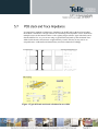
As is often the case board material may be dictated by other applications that are integrated
onto the host board. The board thickness may be such that a very narrow trace may result.
This may not be acceptable and can also lead to issues when the trace meets a component pad.
In situation like this the ground layer directly under the RF trace path can be removed and the
RF ground is then moved to the next layer. This can result in a more acceptable trace width.
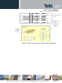
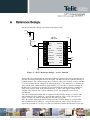
Figure 2 Avoid Narrow RF trace