1
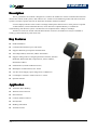
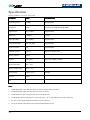
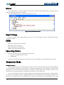
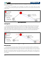
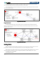
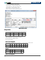
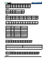
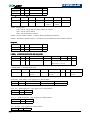
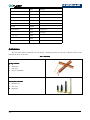
DTMUA5
-4
33
VTVT-DTMUA5
DTMUA5-4
-433
RF Transceiver Module
User
User’’s guide v5.0
深圳市芯威科技有限公司
V-chip Microsystems,Inc
地址:深圳市南山区麒麟路 1 号科技创业服务中心大厦 612-613
Add:612-613, Enterprises Incubator No.1 Qilin Road Nanshan Shenzhen
电话:0755-88844812
Tel:86-755-88844812
传真:0755-22643680
Fax:86-755-22643680
邮箱:[email protected]
E-mail:[email protected]
邮编:518052
ZIP:518052
网站:www.digiRF.com
Web:www.digiRF.com
DTMUA5
-4
33
VTVT-DTMUA5
DTMUA5-4
-433
Description
The VT_DTMUA5-433 module is designed as a wireless sub module for wireless communication between
devices like controls, POS systems, data collectors etc. It offers several addressing modes and relieves the host
systems of wireless-specific task such as checksum calculation, address resolution.
It can be deployed whenever the wireless exchange of data packet between two or more parties is required.
A USB interface (Virtual COM Port Device) whose data rate is adjusted flexibly is available for
communicating with the host systems. The data rate can be adjusted from 2.4kbps to 230.4kbps.
Thanks to its small size and the external SMA antenna connector, the module can easily be installed in
existing systems without any external circuits.
Key Features
�
GFSK modulation
�
Communication distance up to 1200 meter
�
Supports addressing transparent communication
�
Auto add preamble, checksum, address information
�
Supports setting mode to configure parameters Channel, Interface
Band Rate, Radio Data Rate, Output Power, Source Address,
Destination Address
�
USB interface (Virtual COM Port Device)
�
Half Duplex communication, 8N1 format
�
5.0V DC Power Supply, Input voltage from a USB device
�
Consumption: Transmit <250mA; Receive <55mA
�
Optional Antenna
Application
�
Automatic Meter Reading
�
Wireless Sensor Network
�
Data Collector
�
Controls, Remote Controls
�
POS Systems
�
Building Automation
�
Android Controls
Copyright @ 2013 V-chip Microsystems,Inc
v5.0
Version: VTDTMUA5-MARCH-2013
DTMUA5
-4
33
VTVT-DTMUA5
DTMUA5-4
-433
Specification
Testing condition:Ta=25°C, VCC=5.0V
Parameter
Value
Condition/Note
Center Frequency
433MHz
Programmable
Modulation
GFSK
Customize for ASK/FSK/OOK/MSK
Output Power
Max: 27dBm
Programmable
Sensitivity
-110dBm
1.2kbps
Radio Data Rate
Max 500kbps
Programmable
USB Interface Rate
Max 230.4kbps
Programmable
Protocol Format
8N1
Programmable
Transmit Current
<250mA
Depend on output power
Receive Current
<55mA
Distance
1200 meter
Operate Humidity
10%~90%
Operate Temperature
-40℃~85℃
Input Voltage
5.0VDC±10%
Antenna
50ohm
Open area; 27dBm; 2.4kbps
±100mV
Size
Note
Note::
1. Noted that higher radio data rate causes of shorter communication disdance.
2. Noted that higher radio data rate causes of lower sensitivity.
3. Noted that lower input voltage causes of lower output power.
4. Noted that the operate temperature out of range -40℃~85℃ will influence the center frequency.
5. Be sure to use a match antenna and mount it in the right way.
6. The environment will influence the communication disdance much.
Copyright @ 2013 V-chip Microsystems,Inc
v5.0
Version: VTDTMUA5-MARCH-2013
DTMUA5
-4
33
VTVT-DTMUA5
DTMUA5-4
-433
Driver
The USB interface is a virtual COM Port Device base on USB to UART bridge solution. Install the drivers
before connecting the module to a computer.
The virtual COM Port Device can be found as the Fig 1 shows.
Fig 1 Virtual COM Port Device
Input Voltage
The input voltage of the module ranges from 4.5V to 5.5V. A clean supply voltage is needed for the module
to function correctly.
LEDs
There are 3 LEDs install in the module:
RED_LED: Power-on indicates.
BLUE_LED: Receive data indicate.
GREEN_LED: Transmit data indicate.
Operating Modes
The device can be used in the following operating modes:
1. Transceiver, Buffered data transceiver
2. Setting Mode
The device is default on transparent mode and can select by commands. See “Setting Mode” part in detail.
Transceiver Mode
Transparent mode:
In this operating mode, data of the transmitter module is received via the USB interface and initially buffered.
As soon as specific conditions are met (timeout or data buffer be filled full), the radio telegram is generated with
preamble, Sync word, and Checksum and address information (modules address are the same). As soon as the
transmission of a packet has begun, the USB interface cannot receive any further data.
The receiver module receives the wireless telegram and transmits the payload characters via USB interface.
As long as receiver module is busy in sending characters via the USB interface, wireless telegram reception is not
possible. For example, this effect is noticeable when sending a long data packet and subsequently a short data
Copyright @ 2013 V-chip Microsystems,Inc
v5.0
Version: VTDTMUA5-MARCH-2013
DTMUA5
-4
33
VTVT-DTMUA5
DTMUA5-4
-433
packet. In this case, the receiver module may still be busy in sending the first packet via USB interface and the
second packet may be lost.
For example, if the transmitter send “1234567890”, all module in the receive range can receive
“1234567890”. This operating mode supports range extender device that can receive the data and re-transmits data
to other receiver.
Fig 2 Transparent Mode
Addressing mode:
In this operating mode, the transmitter’s source address and destination address need to be the same as the
receiver’s destination address and source address respectively. For example, set the transmitter’s source address
0x0001 and destination address 0x0004, and set the receiver’s source address 0x0004 and destination address
0x0001. The transmitter send “1234567890” then the receiver can receive “1234567890”. This operating mode is
useful in Point-to-Point communication and supports the range extender device that re-transmits data to the
destination module.
Fig 3 Addressing Mode
Master-Slave mode:
In this operating mode, the first 2 bytes of data from the USB is the destination address in the Master side,
the data send to the correct destination address, and the first 2 bytes of data from wireless is the source address, it
tell to the master where the data from. For example, set the master’s source address 0x0001, if we want to send the
data “ABC” to the destination module (source address 0x0002), send data “0x0002+ABC” to the master, then the
destination can receive the data “ABC”. If the master receives data from a slave “0x0004+123”, the 0x0004 is the
slave’s address.
Copyright @ 2013 V-chip Microsystems,Inc
v5.0
Version: VTDTMUA5-MARCH-2013
DTMUA5
-4
33
VTVT-DTMUA5
DTMUA5-4
-433
The destination address and source address do not input or output via the USB in the Slave side, but the
slave’s destination address must set as the same as the master’s source address.
This operating mode is a typically start topology mode and supports range extender device that re-transmits
data to the destination module.
Fig 4 Master-Slave Mode
Range Extend mode:
To extend communication range, range extender can be use in transparent mode, addressing mode and
Master-slave mode. The range extender re-transmits the data to the destination module, and can receive data if
destination address correct.
Fig 5 Master-Slave Mode
Setting Mode
When receiving the Enter Setting Mode command, device enter setting mode. In setting mode, user can set
the parameters. The device stays on setting mode until receive the Exit Setting Mode command.
Some parameters are sending out when power on to help user remember what parameters have set. User can
collect the parameters information correctly if configure the parameter of USB to 9600bps, 8N1, as Fig 6.
“VT-DTMUA5-433”: Part Number
“V01.20 F05.00”: Version
Copyright @ 2013 V-chip Microsystems,Inc
v5.0
Version: VTDTMUA5-MARCH-2013
DTMUA5
-4
33
VTVT-DTMUA5
DTMUA5-4
-433
“SN:0000000000000000”: Serial Number
“UART Baud:03”: UART baud setting value
“UART Option:02”: UART option setting value
“Radio Baud:03”: Radio band setting value
“Radio Channel:03”: Radio Channel setting value
Fig 6 Parameter Collect
Setting Command
All Commands are used HEX format, and the command format is:
Data
SOF
CMD
PLOAD
EOF
Length(byte)
1
1
n
1
Functions
Start Byte
Command Byte
Data Byte
Stop Byte
SOF: Start byte, 0xFD;
CMD: Command byte, indicate different command;
PLOAD: Data bytes, configure content;
EOF: Stop byte, 0xFE。
CMD 1: Enter Setting Mode
If enter setting mode and then set the parameters, the setting parameters will be stored.
Data
Length(byte)
Functions
SOF
CMD
EN1
EN2
EN3
EN4
EN5
EOF
1
1
1
1
1
1
1
1
0xFD
0x00
0x55
0x55
0x55
0x55
0x55
0xFE
SOF
CMD
STATE
EOF
1
1
1
1
0xFD
0x00
0 Success; non-0 Fail
0xFE
Respond:
Data
Length(byte)
Functions
CMD 2: Exit Setting Mode
Copyright @ 2013 V-chip Microsystems,Inc
v5.0
Version: VTDTMUA5-MARCH-2013
DTMUA5
-4
33
VTVT-DTMUA5
DTMUA5-4
-433
Data
SOF
CMD
EN1
EN2
EN3
EN4
EN5
EOF
1
1
1
1
1
1
1
1
0xFD
0xFF
0xAA
0xAA
0xAA
0xAA
0xAA
0xFE
SOF
CMD
STATE
EOF
1
1
1
1
0xFD
0xFF
0 Success; non-0 Fail
0xFE
Data
SOF
CMD
UBAUD
UOPTION
DBAUD
CHANNEL
POWER
EOF
Length(byte)
1
1
1
1
1
1
1
1
Functions
0xFD
0x01
COM Baud
COM Option
RF Baud
Channel
Output Power
0xFE
Length(byte)
Functions
Respond:
Data
Length(byte)
Functions
CMD3:
UBAUD: COM baud
UBAUD
0x00
0x01
0x02
0x03
0x04
0x05
0x06
0x07
0x08
0x09
0x0a
0x0b
Baud
1.2k
2.4k
4.8k
9.6k
14.4k
19.2k
28.8k
38.4k
57.6k
76.8k
115.2k
230.4k
UOPTION: COM Option
UOPTION BIT
Items
Value 1
Value 0
BIT.7
ORDER
MSB
LSB
BIT.6
FLOW
Flow control enable
Flow control disable
BIT.5
D9
ODD-Parity
EVEN-Parity
BIT.4
BIT9
9Bits
8Bits
BIT.3
PARITY
Enable
Disable
BIT.2
SPB
2bits
1bit
BIT.1
STOP
High level
Low level
BIT.0
START
High level
Low level
Note:If parity enable,BIT9 set to 9Bits。
DBAUD:RF Baud:
UBAUD
0x00
0x01
0x02
0x03
0x04
0x05
0x06
0x07
0x08
0x09
Baud
1.2k
2.4k
4.8k
9.6k
19.2k
38.4k
76.8k
100k
250k
500k
CHANNEL:Channel:
CHANNAL
0x00~0x32
Frequency Range
428MHz~438MHz
Note:
Supports 51 channels, channel spacing 200kHz, the channel 0 frequency is 428MHz, and the channel 50 frequency is 438MHz.
POWER:RF output power:
POWER(Hex)
C0
63
68
6C
28
26
25
1F
32
19
0E
0B
08
07
05
04
03
Po(dBm)
27
23
20
17
15
13
11
9
7
5
3
1
-1
-3
-5
-7
-9
Respond
Respond:
Copyright @ 2013 V-chip Microsystems,Inc
v5.0
Version: VTDTMUA5-MARCH-2013
DTMUA5
-4
33
VTVT-DTMUA5
DTMUA5-4
-433
Data
Length(byte)
Functions
SOF
CMD
STATE
EOF
1
1
1
1
0xFD
0x01
0 Success; non-0 Fail
0xFE
Address setting
CMD4
CMD4:Address
Data
SOF
CMD
TYPE
SADD
DADD
EOF
Length(byte)
1
1
1
2
2
1
Functions
0xFD
0x02
Setting Type
Source
Destination
0xFE
address
address
TYPE:Setting Type,
0x00-Set the source address and the destination address;
0x01-Set the source address;
0x02-Set the destination address。
SADD:Source Address :0x0001~0xFFFE; Reserved 0x0000 and 0xFFFF;
DADD:Destination Address 0x0001~0xFFFE; Reserved 0x0000; Broadcast address 0xFFFF。
Respond
Respond:
Data
Length(byte)
Functions
SOF
CMD
STATE
EOF
1
1
1
1
0xFD
0x02
0 Success; non-0 Fail
0xFE
Communication mode and sleep mode
CMD5
CMD5:Communication
Data
Length(byte)
Functions
SOF
CMD
COMOPTION
SLPTYPE
TWOR_SlEEP
TWOR_RX
TRX
EOF
1
1
1
1
1
1
1
1
0xFD
0x03
Communication mode
Sleep mode
BIT7:0 (s),1 (ms)
0xFE
BIT6-BIT0:Time tick
COMOPTION:Communication mode
COMOPTION
0x00
0x01
0x02
0x03
0x04
0x05
0x06
Mode
Transparent
Transparent range
Addressing
Addressing range
Master
Slave
Master-Slave range
extender
extender
extender
SLPTYPE:Sleep Mode(only supports for UART module)
SLPTYPE
0x00
0x01
0x02
0x03
Mode
Not sleep
Sleep-wake up by UART
Sleep-wake up by I/O
Sleep-wake up by RF
TWOR_SlEEP:WOR sleep time(only supports for UART module)
TWOR_SlEEP
BIT.7
BIT.6-BIT.0
Time
s/ms
Time
TWOR_RX:WOR Rx timeout(only supports for UART module)
TWOR_RX
BIT.7
BIT.6-BIT.0
Rx Timeout
s/ms
Time
TRX:Rx time(only supports for UART module)
TRX
BIT.7
BIT.6-BIT.0
Copyright @ 2013 V-chip Microsystems,Inc
v5.0
Version: VTDTMUA5-MARCH-2013
DTMUA5
-4
33
VTVT-DTMUA5
DTMUA5-4
-433
Rx Time
s/ms
Time
Respond
Respond:
Data
Length(byte)
Functions
SOF
CMD
STATE
EOF
1
1
1
1
0xFD
0x03
0 Success; non-0 Fail
0xFE
SOF
CMD
TYPE
EOF
1
1
1
1
0xFD
0x04
0x00 Read all parameters
0xFE
命令六:读设置
Data
Length(byte)
Functions
0x01 Read UART Baud rate
0x02 Read UART Option
0x03 Read RF Baud rate
0x04 Read Channel
0x05 Read output power
0x06 Read source address
0x07 Read destination address
0x08 Read communication mode
0x09 Read sleep mode
0x0a Read Rx timeout
0x0b Read WOR sleep time
0x0c Read WOR Rx timeout
Respond
Respond:
Data
Lengfh(bytes)
Functions
SOF
1
0xFD
CMD
1
0x04
UBAUD
1
UART Baud rate
UOPTION
1
UART Option
DBAUD
1
RF Baud rate
CHANNEL
1
Channel
POWER
1
Output power
SADD
1
Source address
DADD
1
Destination address
COMOPTION
1
Communication Mode
SLPTYPE
1
Sleep Mode
TWOR_SlEEP
1
WOR sleep time
TWOR_RX
1
WOR Rx timeout
TRX
1
Rx timeout
EOF
1
0xFE
Note:
Default Parameters:
Item
Parameter
Copyright @ 2013 V-chip Microsystems,Inc
v5.0
Describe
Version: VTDTMUA5-MARCH-2013
DTMUA5
-4
33
VTVT-DTMUA5
DTMUA5-4
-433
UBAUD
0x03
9600bps
UOPTION
0x02
8N1
DBAUD
0x03
9600bps
CHANNEL
0x00
428MHz
POWER
0xC0
27dBm
SADD
0x0001
DADD
0x0001
COMOPTION
0x00
Transparent
SLPTYPE
0x00
Not sleep
TWOR_SlEEP
0x00
/
TWOR_RX
0x00
/
TRX
0x00
/
Antennas
We offer many kinds of antennas. We can design a matching antenna for specific conditions. Some of the
antennas are show on the Tab 2.
Tab 1 Antennas
Spring Antenna
� Small size
� Low cost
� Easy to embedded
SMA Plastic Antenna
� Medium size
� Low cost
� High gain
Copyright @ 2013 V-chip Microsystems,Inc
v5.0
Version: VTDTMUA5-MARCH-2013
DTMUA5
-4
33
VTVT-DTMUA5
DTMUA5-4
-433
Sucker Antenna
� High gain
� Have sucker
� Easy to fix
Troubles and Processing Methods
Troubles
Processing Methods
1. Check the input voltage; ensure it is not lower than 4.5VDC.
2. Configure the output power parameter to the max.
Short distance
3. Check the antenna; ensure it is not to be shielded.
4. Configure the radio data rate to a lower value.
1. Check the input voltage.
Communicating
failed
2. Reconnect the module to the host.
3. Addresses of the communicating modules are all right.
4. LEDs flash while transmission or reception.
1. Antenna does not match to the module.
High error rate
2. Co-Channel interference, try another channel.
IMPORTANT NOTICE
V-chip Microsystems,Inc. (short of V-chip)reserve the right to make corrections, modifications, enhancements,
improvements, and other changes to its products and services at any time and to discontinue any product or
service without notice. Customers should obtain the latest relevant information before placing orders and should
verify that such information is current and complete. All products are sold subject to V-chip’s terms and
conditions of sale supplied at the time of order acknowledgment.
V-chip warrants performance of its hardware products to the specifications applicable at the time of sale in
accordance with V-chip’s standard warranty. Testing and other quality control techniques are used to the extent
V-chip deems necessary to support this warranty.
V-chip does not warrant or represent that any license, either express or implied, is granted under any V-chip
patent right, copyright, mask work right, or other V-chip intellectual property right relating to any combination,
machine, or process in which V-chip products or services are used. Information published by V-chip regarding
third-party products or services does not constitute a license from V-chip to use such products or services or a
warranty or endorsement thereof. Use of such information may require a license from a third party under the
patents or other intellectual property of the third party, or a license from V-chip under the patents or other
intellectual property of V-chip.
Copyright @ 2013 V-chip Microsystems,Inc
v5.0
Version: VTDTMUA5-MARCH-2013
DTMUA5
-4
33
VTVT-DTMUA5
DTMUA5-4
-433
Reproduction of V-chip information in V-chip data books or data sheets is permissible only if reproduction is
without alteration and is accompanied by all associated warranties, conditions, limitations, and notices.
Reproduction of this information with alteration is an unfair and deceptive business practice. V-chip is not
responsible or liable for such altered documentation. Information of third parties may be subject to additional
restrictions.
Resale of V-chip products or services with statements different from or beyond the parameters stated by V-chip
for that product or service voids all express and any implied warranties for the associated V-chip product or
service and is an unfair and deceptive business practice. V-chip is not responsible or liable for any such
statements.
Copyright @ 2013 V-chip Microsystems,Inc
v5.0
Version: VTDTMUA5-MARCH-2013