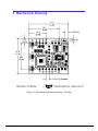
Download User Guide
Transcript
User Manual MicroMagIC™ 3 Axis High Data Rate Magnetic Sensor Module Table of Contents 1 COPYRIGHT & WARRANTY INFORMATION .............................................................. 3 2 OVERVIEW..................................................................................................................... 4 3 SPECIFICATIONS .......................................................................................................... 5 4 TYPICAL OPERATING CHARACTERISTICS .............................................................. 6 5 MECHANICAL DRAWING ............................................................................................. 8 6 SET-UP ......................................................................................................................... 10 6.1 PCB ORIENTATION AND OUTPUT POLARITIES ...................................... 10 6.2 BOARD CONNECTIONS AND TEST POINTS ............................................ 11 6.3 CLOCK OPTIONS......................................................................................... 13 7 OPERATION................................................................................................................. 16 7.1 MAKING A MEASUREMENT........................................................................ 16 7.1.1 Slave Select ..................................................................................... 17 7.1.2 Idle Mode ......................................................................................... 18 7.1.3 SPI Interface Considerations ........................................................... 18 7.2 REGISTER DEFINITION .............................................................................. 19 List of Figures Figure 4-1: Figure 4-2: Figure 4-3: Figure 4-4: Figure 5-1: Figure 5-1: Figure 6-1: Figure 6-2: Figure 6-3: Figure 6-4: Figure 6-5: Figure 7-1: Figure 7-2: Period Select vs. Data Rate per Axis ....................................................... 6 Output Counts vs. Magnetic Field and Temperature ............................... 6 Linearity vs. Temperature ........................................................................ 7 Repeatability and Hysteresis ................................................................... 7 MicroMagIC Mechanical Drawing – Top View ......................................... 8 MicroMagIC Mechanical Drawing – Side View ........................................ 9 MicroMagIC Orientation ......................................................................... 10 Default Strap Configuration ................................................................... 13 Strapping Configuration for Clock Source.............................................. 14 Strapping Configuration for Clock Output .............................................. 15 Strapping Configuration for Clock Speed ............................................... 15 SPI Interface Sequence ......................................................................... 17 SPI Interface Timing .............................................................................. 17 List of Tables Table 3-1: Table 3-2: Table 6-1: Table 6-2: Table 7-1: Table 7-2: Absolute Maximum Ratings ....................................................................... 5 Module Characteristics1 ............................................................................ 5 Board Connection Pin-Out .......................................................................11 Test Points ............................................................................................... 13 Command Register ................................................................................. 19 Results Register ...................................................................................... 20 深圳市铭之光电子技术有限公司 全国服务热线 : 400-883-3391 http://www.sensorexpert.com.cn 1 Copyright & Warranty Information © Copyright PNI Sensor Corporation 2009 All Rights Reserved. Reproduction, adaptation, or translation without prior written permission is prohibited, except as allowed under copyright laws. Revised April 2009: for the most recent version visit our website at www.pnicorp.com PNI Sensor Corporation 133 Aviation Blvd, Suite 101 Santa Rosa, CA 95403, USA Tel: (707) 566-2260 Fax: (707) 566-2261 Warranty and Limitation of Liability. PNI Sensor Corporation ("PNI") manufactures its Products from parts and components that are new or equivalent to new in performance. PNI warrants that each Product to be delivered hereunder, if properly used, will, for one year following the date of shipment unless a different warranty time period for such Product is specified: (i) in PNI’s Price List in effect at time of order acceptance; or (ii) on PNI’s web site (www.pnicorp.com) at time of order acceptance, be free from defects in material and workmanship and will operate in accordance with PNI’s published specifications and documentation for the Product in effect at time of order. PNI will make no changes to the specifications or manufacturing processes that affect form, fit, or function of the Product without written notice to the Customer, however, PNI may at any time, without such notice, make minor changes to specifications or manufacturing processes that do not affect the form, fit, or function of the Product. This warranty will be void if the Products’ serial number, or other identification marks have been defaced, damaged, or removed. This warranty does not cover wear and tear due to normal use, or damage to the Product as the result of improper usage, neglect of care, alteration, accident, or unauthorized repair. THE ABOVE WARRANTY IS IN LIEU OF ANY OTHER WARRANTY, WHETHER EXPRESS, IMPLIED, OR STATUTORY, INCLUDING, BUT NOT LIMITED TO, ANY WARRANTY OF MERCHANTABILITY, FITNESS FOR ANY PARTICULAR PURPOSE, OR ANY WARRANTY OTHERWISE ARISING OUT OF ANY PROPOSAL, SPECIFICATION, OR SAMPLE. PNI NEITHER ASSUMES NOR AUTHORIZES ANY PERSON TO ASSUME FOR IT ANY OTHER LIABILITY. If any Product furnished hereunder fails to conform to the above warranty, Customer’s sole and exclusive remedy and PNI’s sole and exclusive liability will be, at PNI’s option, to repair, replace, or credit Customer’s account with an amount equal to the price paid for any such Product which fails during the applicable warranty period provided that (i) Customer promptly notifies PNI in writing that such Product is defective and furnishes an explanation of the deficiency; (ii) such Product is returned to PNI’s service facility at Customer’s risk and expense; and (iii) PNI is satisfied that claimed deficiencies exist and were not caused by accident, misuse, neglect, alteration, repair, improper installation, or improper testing. If a Product is defective, transportation charges for the return of the Product to Customer within the United States and Canada will be paid by PNI. For all other locations, the warranty excludes all costs of shipping, customs clearance, and other related charges. PNI will have a reasonable time to make repairs or to replace the Product or to credit Customer’s account. PNI warrants any such repaired or replacement Product to be free from defects in material and workmanship on the same terms as the Product originally purchased. Except for the breach of warranty remedies set forth herein, or for personal injury, PNI shall have no liability for any indirect or speculative damages (including, but not limited to, consequential, incidental, punitive and special damages) relating to the use of or inability to use this Product, whether arising out of contract, negligence, tort, or under any warranty theory, or for infringement of any other party’s intellectual property rights, irrespective of whether PNI had advance notice of the possibility of any such damages, including, but not limited to, loss of use, revenue or profit. In no event shall PNI’s total liability for all claims regarding a Product exceed the price paid for the Product. PNI neither assumes nor authorizes any person to assume for it any other liabilities. Some states and provinces do not allow limitations on how long an implied warranty lasts or the exclusion or limitation of incidental or consequential damages, so the above limitations or exclusions may not apply to you. This warranty gives you specific legal rights and you may have other rights that vary by state or province. 深圳市铭之光电子技术有限公司 全国服务热线 : 400-883-3391 http://www.sensorexpert.com.cn 2 Overview Thank you for purchasing PNI Sensor Corporation’s MicroMagIC (PNI part number 12800). The MicroMagIC is an integrated 3-axis high-data-rate magnetic field sensing module combining PNI’s patented SmartSens magneto-inductive (MI) sensors with PNI’s MagIC high-data-rate driver ASIC. Designed primarily to aid in the evaluation and prototyping of PNI’s SmartSens technology, the MicroMagIC board contains connectors, test points, option solder jumpers and extra support circuits to expedite evaluation. The microprocessorcompatible SPI interface allows easy access to the MicroMagIC’s measurement parameters and resulting field measurement data. PNI’s MicroMagIC benefits include low power consumption, large signal noise immunity under all conditions, a large dynamic range, and high sampling rates. Measurements are very stable over temperature and inherently free from offset drift. Also, the MicroMagIC features software-configurable resolution, sample rate and field measurement range. These advantages make PNI’s MicroMagIC not only the choice for prototyping high volume SmartSens solutions, but also for lower volume applications that require a complete solution. PNI’s SmartSens product line also includes the Sen-XY™ and Sen-Z™ magneto-inductive sensors, MagIC and 11096 ASICs, MS2100™ single-chip solution, and the MicroMag2™ and MicroMag3™, The primary difference between the MicroMagIC (with MagIC ASIC) and MicroMag2/3 (with 11096 ASIC) is the data rate at which the module can operate: the MagIC can provide about 8x the data rate for comparable resolution. The user may wish to refer to PNI’s MagIC (ASIC) User Manual for more detailed information on the MagIC operation and underlying functionality. 深圳市铭之光电子技术有限公司 全国服务热线 : 400-883-3391 http://www.sensorexpert.com.cn 3 Specifications Table 3-1: Absolute Maximum Ratings Parameter Symbol Maximum DC Supply Voltage VDD 3.75 VDC Digital Input Voltage VIN -0.3V to 3.6V CAUTION: Stresses beyond those listed Table 3-1 may cause permanent damage to the device. These are stress ratings only. Functional operation of the device at these or any other conditions beyond those indicated in the operational sections of the specifications is not implied. Exposure to absolute maximum rating conditions for extended periods may affect device reliability. Table 3-2: Module Characteristics1 Parameter Min Resolution2 (1/Gain), PS = 512 Max 0.6 3 Field Measurement Range -1100 4 1 % +1100 μT 165 kHz 68 count/μT PS = 32 1.7 mA rms PS = 1024 3.6 mA rms 55 μA rms 2 Gain , PS = 512 Continuous Current, measured at MagIC ASIC VCC Units μT 0.015 Linearity, best fit straight line over ±300 μT Sensor Frequency Typ. Idle current, measured at MagIC ASIC VCC Recommended DC Power Supply Voltage (VDD) 2.7 Operating Temperature Storage Temperature 3.3 3.6 VDC -40 +85 C -40 +85 C Notes: 1) Power supply voltage (VDD) = 3.3 VDC. “PS” is the “period select”, which is set by the user in software, and is inversely proportional to the data rate, as show in Figure 4-1. 2) The Gain and Resolution can be increased by a factor of 8 by setting the period select to 4095. However, the ASIC counter can overflow if the field is strong enough to drive the count beyond a signed 20-bit signed integer. In practical magnetometer applications, a sensor gain calibration is optimally performed when the sensor module is in the host system. Also, noise can limit attainable resolution. 3) Field Measurement Range is defined as the monotonic region of the output characteristic curve. 4) Sensor frequency is defined within free the Earth’s magnetic field. 深圳市铭之光电子技术有限公司 全国服务热线 : 400-883-3391 http://www.sensorexpert.com.cn 4 Typical Operating Characteristics Figure 4-1: Period Select vs. Data Rate per Axis OUTPUT COUNTS (PS=512) 60000 -25C 0C 25C 50C 75C 50000 40000 30000 20000 10000 0 0 500 1000 1500 2000 MAGNETIC FIELD (µT) Figure 4-2: Output Counts vs. Magnetic Field and Temperature 深圳市铭之光电子技术有限公司 全国服务热线 : 400-883-3391 http://www.sensorexpert.com.cn OUTPUT COUNTS (PS=512) 24000 -25C 0C 25C 50C 75C 20000 16000 12000 8000 4000 0 0 50 100 150 200 250 300 MAGNETIC FIELD (µT) Figure 4-3: Linearity vs. Temperature OUTPUT COUNTS (PS=512) 50000 1st Cycle 40000 2nd Cycle 30000 4th Cycle 3rd Cycle 5th Cycle 20000 10000 0 -2000 -10000 -1500 -1000 -500 0 500 1000 1500 2000 -20000 -30000 -40000 -50000 MAGNETIC FIELD (µT) Figure 4-4: Repeatability and Hysteresis 深圳市铭之光电子技术有限公司 全国服务热线 : 400-883-3391 http://www.sensorexpert.com.cn 5 Mechanical Drawing Figure 5-1: MicroMagIC Mechanical Drawing – Top View 深圳市铭之光电子技术有限公司 全国服务热线 : 400-883-3391 http://www.sensorexpert.com.cn Figure 5-2: MicroMagIC Mechanical Drawing – Side View 深圳市铭之光电子技术有限公司 全国服务热线 : 400-883-3391 http://www.sensorexpert.com.cn 6 Set-Up 6.1 PCB Orientation and Output Polarities The magneto-inductive sensors on the MicroMagIC PCB are arranged in the north-eastdown (NED) coordinate system. That is, the positive terminals for the X, Y and Z axis sensors point in the NED directions, respectively, when the arrow printed on the board is pointing north and the board is lying flat and level. The resulting polarity of the output data is such that when the direction arrow on the board is facing north the X-axis value will be positive, when the board is pointing west (Y-axis positive terminal is pointing north) the Yaxis value will be positive, and when the board is sitting level the Z-axis, which is pointing down, will be positive in the northern hemisphere and negative in the southern hemisphere. Magnetometer Polarities Earth’s Magnetic North pole this way Polarity of MagIC data output relative to position of board reference arrow to magnetic North Position Axis X Y Z N W S E + 0 0 0 + 0 0 0 0 0 N N Top Bottom 0 0 - 0 0 + X+ L2 L2 (Y) (Y) L1(X) on Bottom X L3 (Z) Y+ Z+ (DOWN) TOP view of PCB Orientation of sensors is N.E.D. (North East Down) for X, Y, Z sensors positive leads as they relate to the MagIC pin nomenclature Positive terminal of component is denoted with a dot Source: uMagIC_Orientation.vsd Figure 6-1: MicroMagIC Orientation 深圳市铭之光电子技术有限公司 全国服务热线 : 400-883-3391 http://www.sensorexpert.com.cn 6.2 Board Connections and Test Points The MicroMagIC PCB contains three connectors, J7, J8, and J9, as identified on the underside of the PCB. Connector pins are labeled on top of the board, as can be seen in Figure 5-1. The pin-out is summarized in Table 6-1, with descriptions following the table. Note the MicroMagIC is configured to run as a slave device in a master/slave configuration. Table 6-1: Board Connection Pin-Out Connector Board Number Identifier J7 J8 J9 MagIC Equivalent Description SCK SCLK SPI Serial Clock Input SO MISO SPI Serial Out SI MOSI SPI Serial In RDY DRDY Data Ready RST RESET Reset GND - Ground NC - No connection ~PD NA ~SL - ~SS SSNOT SPI Slave Select Input VDD VCCIO 3.3V Power input NC - No connection GND - Ground Power Down No connection SCK (SPI Serial Clock Input) An SPI input is used to synchronize both the data in and out through the SO and SI lines. SCK is generated by the customer-supplied master device and should be 1 MHz or less. One byte of data is exchanged over eight clock cycles. The SCK line is referred to in the MagIC manual as the SCLK line, which is the common SPI term. SO (SPI Serial Out) An SPI output that sends data from the MicroMagIC to the master device. Data is transferred most significant bit first and is captured by the master device on the rising edge of SCK. The SO line is referred to in the MagIC manual as the MISO (Master In, Slave Out) line, which is the common SPI term. 深圳市铭之光电子技术有限公司 全国服务热线 : 400-883-3391 http://www.sensorexpert.com.cn SI (SPI Serial In) An SPI input that provides data from the master device to the MicroMagIC. Data is transferred most significant bit first. Data must be presented at least 100 ns before the rising edge of SCK, and remain valid for 100 ns after the edge. New data may be presented to the SI pin on the falling edge of SCK. The SI line is referred to in the MagIC manual as the MOSI (Master Out, Slave In) line, which is the common SPI term. RDY (Data Ready) It is recommended the RDY line be used to ensure data is clocked out of the MicroMagIC only when it is available. RDY is set low after a RESET. After a command has been received and the data is ready, RDY will be changed to high. The RDY line is referred to in the MagIC manual as DRDY. RST (Reset) RST must be toggled from low-high-low before sending a measurement command. RST is usually low. The RST line is referred to as the RESET line in the MagIC manual. ~PD (Power Down) This signal has a pull-up resistor tied to VDD. When pulled to ground, it will turn off the core voltage regulator of the MagIC device. Note this is only a MicroMagIC feature and not a MagIC signal. ~SS (SPI Slave Select) This signal sets the MicroMagIC as the operating slave device on the SPI bus. The ~SS line must be LOW prior to data transfer in either direction, and must stay LOW during the entire transfer. The SPI bus can be freed up (~SS line set HIGH) for communication with another slave device while the MicroMagIC is taking a measurement or idle, but after all communication between the MicroMagIC and master device is finished. VDD (3.3 VDC Input) The user should supply 3.3 VDC on this line. The bias resistor values for the three magnetometers were optimized for 3.3 VDC operation. The board can be run at other voltages within the specifications of the MagIC. Refer to the test sheet for optimal bias resistor values for other operating voltages. The MicroMagIC PCB incorporates a couple of test points which are identified on the top of the PCB and summarized in Table 6-2. (See Figure 6-2 for the locations of XI and XO.) 深圳市铭之光电子技术有限公司 全国服务热线 : 400-883-3391 http://www.sensorexpert.com.cn Table 6-2: Test Points Board Identifier Description XI External Clock input signal. XO Clock signal output for monitoring or daisy chain internal or external clock. GND Ground 6.3 Clock Options The MicroMagIC can be configured for various clock options, including: type of clock (internal, external, or crystal oscillator), outputting or not outputting the clock, and dividing the clock rate by 2. In its default configuration, the MicroMagIC will operate using a crystal oscillator clock mounted on the MicroMagIC board at full speed and the signal will be output. Changes to the clock options are made by altering the solder jumpers on pins S1 – S6. Figure 6-2shows the default configuration, while other clock configurations are shown in Figure 6-3, Figure 6-4 and Figure 6-5. Figure 6-2: Default Strap Configuration It is critical a jumper be in place for S1, S2, and S3 such that no input is left floating. Pull-up/pull-down resistors were not incorporated into the MicroMagIC so current consumption can more accurately reflect a user’s final design (assuming the MicroMagIC is being used for prototyping work in a user’s system). 深圳市铭之光电子技术有限公司 全国服务热线 : 400-883-3391 http://www.sensorexpert.com.cn Clock Source Required strapping Internal Clock (see Figure 6-4 and Figure 6-5) External Clock (see Figure 6-4 and Figure 6-5) Crystal Clock Default position. (see Figure 6-5) Figure 6-3: Strapping Configuration for Clock Source 深圳市铭之光电子技术有限公司 全国服务热线 : 400-883-3391 http://www.sensorexpert.com.cn Clock Output Strapping Option Clock output enabled. Monitor on “XO” test pad Default position. Output clock signal disabled. (Not possible when clock is crystal oscillator.) Figure 6-4: Strapping Configuration for Clock Output Clock Speed Strapping Options Default position Divide clock source by 2 Figure 6-5: Strapping Configuration for Clock Speed 深圳市铭之光电子技术有限公司 全国服务热线 : 400-883-3391 http://www.sensorexpert.com.cn 7 Operation Data flow to and from the MicroMagIC is through a hardware handshaking, synchronous serial interface that adheres to the SPI bus protocol. Section 6.2 reviews the various interface lines and provides brief descriptions of their functions. The user may wish to refer to the MagIC User Manual for a more detailed discussion on the underlying operation of the MagIC driver ASIC, although this is not necessary. (The MagIC ASIC interface is based on PNI’s 11096 ASIC interface except the command is changed from 8 bit to 32 bit. The new command word contains similar sensor axis select bits together with startup and period preset values. The measured result is now extended to signed 20bit value, compared to 16 bit in the PNI’s 11096 ASIC.) 7.1 Making a Measurement The steps to make a sensor measurement are given below, and the sequence and timing are given in Figure 7-1 and Figure 7-2. In general, the user sends a command word (see Section 7.2) to the MicroMagIC through the SPI port specifying the sensor to be measured. After dividing by the Period Select (PS) value, the MicroMagIC returns the result of a complete forward - reverse measurement of the sensor in a 20-bit 2’s complement format (range: -524288 to 524287). Note that only one sensor can be measured at a time. 1. ~SS pin is set LOW. (This enables communication with the master device.) 2. RST pin is set HIGH, then LOW. This will reset the MagIC. 3. A command word is clocked into the MicroMagIC on the SI pin. Once 32 bits have clocked in, the MicroMagIC will execute the command (take a measurement). 4. A measurement consists of forward biasing the sensor and making a period count; then reverse biasing the sensor and counting again; and then taking the difference between the two directions. 5. At the end of the measurement, the RDY line is set HIGH, indicating data is ready. The data is clocked out on the SO pin with the next 20 clock cycles. 深圳市铭之光电子技术有限公司 全国服务热线 : 400-883-3391 http://www.sensorexpert.com.cn Figure 7-1: SPI Interface Sequence ~SS SCK SI SO Figure 7-2: SPI Interface Timing 7.1.1 Slave Select Keeping the ~SS line LOW dedicates the master device to the MicroMagIC. If the user has no other slave devices, the ~SS line can be permanently grounded. Conversely, if the user has multiple slave devices, then the SPI bus can be freed up for other devices by bringing the ~SS line HIGH. The ~SS line can be brought HIGH either: • after sending the command word on the SI line but before setting the RDY line HIGH in order to receive the measurement data on the SO line, and/or 深圳市铭之光电子技术有限公司 全国服务热线 : 400-883-3391 http://www.sensorexpert.com.cn • after receiving the measurement data on the SO line, but before initiating another measurement sequence. 7.1.2 Idle Mode The MicroMagIC incorporates an idle mode to reduce power consumption, in which it automatically goes to sleep when it is not exchanging data or taking a measurement. However, it does not necessarily initialize in the idle mode at power-up. To ensure the MicroMagIC will be in idle mode after being turned on, it is necessary to cycle the MagIC through one measurement operation. 7.1.3 SPI Interface Considerations When implementing an SPI port, whether a dedicated hardware peripheral port or a software-implemented port using general purpose I/O (also known as Bit-Banging), the timing parameters (given in Figure 7-2) must be met to ensure reliable communications. The clock set-up and hold times, tDBSH and tDASH must be greater than 100 ns. Also note that an SPI port can be implemented using different clock polarity options. The clock polarity used with the MicroMagIC must be normally low, (cpol = 0). Data always is considered valid while SCK is high (tDASH = Time, Data After SCLK High). When SCK is low, data is in transition (tDBSH = Time, Data Before SCLK High) 深圳市铭之光电子技术有限公司 全国服务热线 : 400-883-3391 http://www.sensorexpert.com.cn 
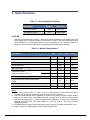
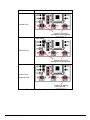
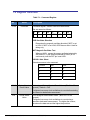
7.2 Register Definition Table 7-1: Command Register Bit 31:24 Name Command Description Command register. Initiates a sensor measurement. Bits are named as follows: 31 30 29 28 27 26 25 ODIR MOT ASI 24 AS0 ODIR Oscillator Direction Determines the magnetic oscillator direction if MOT is set to HIGH. If MOT is set LOW, ODIR has no effect. Used for debug only. MOT Magnetic Oscillator Test When set HIGH, causes the sensor oscillator (selected by AS0 and AS1, in the direction selected by ODIR) to run continuously until the RST pin is set HIGH. AS0-AS1 Axis Select Determines sensor to be measured. 23:16 Startup Counter Preset Value Function AS1 AS0 X 0 0 X 0 1 Y 1 0 Z 1 1 5 bit unsigned Startup Counter Preset Value. (Bits 21 to 23 are ignored). Default = 0x0F Configures how many clock oscillations to count before starting the forward or backward measurement. 15:0 Period Select Value 12 bit unsigned Period Select Value. (Bits 12 to 15 are ignored). Configures how many clock oscillations to count during a forward or backward measurement. The higher the number, the slower the data rate and the higher the precision. 深圳市铭之光电子技术有限公司 全国服务热线 : 400-883-3391 http://www.sensorexpert.com.cn Table 7-2: Results Register Bit Name 19:0 Measured Sensor Value Description Returns measured sensor value in a 20 bit signed value with ranges from -219 to 219-1 (2’s complement number). Zero’s will be returned on SO if more than 20 clock cycles are sent during a read. 深圳市铭之光电子技术有限公司 传感器专家网 E-mail: [email protected] Tel: 400-883-3391 Web : www.sinocomopto.com Web : www.sensorexpert.com.cn 深圳 上海 北京 香港 地址:深圳市福田区天安数 地址:上海市普陀区江宁路1165 地址:北京海淀区中关村东路 地址:香港葵涌嘉庆路12号港 码城创新科技广场1期A座401 号圣天地商务中心705室 66号世纪科贸大厦C座1003室 美中心1004室 电话:(86)0755-83439588 电话:(86)021-52527755 电话:(86)010-62672430 电话:(852)24208555 传真:(86)0755-83433488 传真:(86)021-52522211 传真:(86)010-62672433 传真:(852)24200055