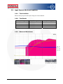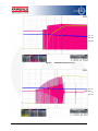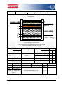
1
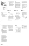
User Guide for FEBFSEZ1317WA_CH310v3 Evaluation Board Primary-Side-Regulation PWM Controller FSEZ1317WAMY 5.0V/0.7A Mobile Phone Battery Charger Featured Fairchild Product: FSEZ1317WA Direct questions or comments about this Evaluation Board to: “Worldwide Direct Support” Fairchild Semiconductor.com © 2012 Fairchild Semiconductor Corporation 1 FEBFSEZ1317WA_CH310v3 • Rev. 1.0.0 Table of Contents 1. Introduction ............................................................................................................................... 3 2. General Specifications .............................................................................................................. 3 3. Functional Test Report.............................................................................................................. 4 3.1. 3.2. 3.3. 3.4. 3.5. 3.6. 3.7. 3.8. 3.9. 3.10. 3.11. 3.12. 3.13. 3.14. 3.15. 3.16. 3.17. Input Current ................................................................................................................. 4 Input Power at No-Load Condition............................................................................... 5 Line Regulation and Load Regulation .......................................................................... 7 Efficiency ...................................................................................................................... 7 Output Ripple and Noise ............................................................................................... 8 Step Response ............................................................................................................. 10 Over-Power Protection................................................................................................ 11 Hold-up Time .............................................................................................................. 11 Measured Waveforms ................................................................................................. 12 Short-Circuit Protection .............................................................................................. 13 Brownout Test ............................................................................................................. 14 VDD Voltage Level ...................................................................................................... 14 Voltage Stress on MOSFET & Rectifiers ................................................................... 18 Constant Voltage (CV) and Constant Current (CC) Curves ....................................... 20 EMI Test (Output with 1.8M Cable Wire).................................................................. 21 Surge test ..................................................................................................................... 23 ESD Test ..................................................................................................................... 23 4. Photographs............................................................................................................................. 24 5. Circuit Schematic .................................................................................................................... 25 6. PCB Layout ............................................................................................................................. 26 7. 76-B070063-00 FSEZ1317WA Evaluation Board BOM ....................................................... 27 8. Specification Approval ........................................................................................................... 28 9. Revision History ..................................................................................................................... 32 © 2012 Fairchild Semiconductor Corporation 2 FEBFSEZ1317WA_CH310v3 • Rev. 1.0.0 This user guide supports the evaluation board for the FSEZ1317WA. It should be used in conjunction with the datasheet as well as Fairchild’s application notes and technical support team. Please visit Fairchild’s website at www.fairchildsemi.com. This kit supercedes the FEBFSEZ1317A_CH310v3. The revised kit incorporates the next generation FSEZ1317WA, which implements a new frequency hopping method. 1. Introduction This document describes a 3.5W power supply using an FSEZ1317WAMY device. This power supply is targeted for mobile phone battery chargers for a 30mW solution with high efficiency. The controller used on the board is Fairchild Semiconductor’s FSEZ1317WAMY. This third-generation Primary-Side-Regulation (PSR) PWM controller with integrated MOSFET and improved EMI performance provides several features to enhance the performance of low-power flyback converters. The proprietary TRUECURRENT® technology enables precise Constant Current (CC) regulation and simplified circuit design for battery-charger applications. The result is a lower-cost, smaller, and lighter charger compared to conventional designs or a linear transformer. To minimize standby power consumption (30mW at 265VAC), a proprietary Green Mode provides off-time modulation to linearly decrease PWM frequency under light-load conditions. Green Mode assists the power supply in meeting power conservation requirements. By using the FSEZ1317WA, a charger can be implemented with few external components and minimized cost. A typical output CV/CC (Constant Voltage / Constant Current) characteristic envelope is shown in Figure 23 and Figure 24. 2. General Specifications Specification Min. Max. Units Voltage 90 264 VAC Frequency 47 63 Hz Output Voltage 4.75 5.25 V Output Current 0 0.7 A 0 3.5 W Input Output Total Output Power Full-Load Output Power Note: 1. All results tested with output DC cable, AWG 26, 1.8M. © 2012 Fairchild Semiconductor Corporation 3 FEBFSEZ1317WA_CH310v3 • Rev. 1.0.0 3. Functional Test Report Test Model Test Date Test Temperature FEBFSEZ1317WA_CH310v3 July 27, 2012 Ambient AC Source: 6800 Series AC POWER SOURCE Test Equipment Electronic Load: Chroma 63030 Power Meter: WT210 Oscilloscope: TDS3014B Test Items 3.1. 1. Input current 2. Input power at no-load condition 3. Startup time 4. DC output rising time 5. Line regulation and load regulation 6. Efficiency 7. Output ripple and noise 8. Step response 9. Over-current protection 10. Hold-up time 11. Short-circuit protection 12. Brownout test 13. VDD voltage level 14. Voltage stress on MOSFET and rectifier 15. Constant voltage and constant current curve 16. EMI test 17. Surge Test 18. ESD test Input Current 3.1.1. Test Condition Measure the AC input current at maximum load. 3.1.2. Test Result © 2012 Fairchild Semiconductor Corporation Input Voltage Input Current 90V / 60Hz 96.73mA 264V / 50Hz 49.14mA 4 FEBFSEZ1317WA_CH310v3 • Rev. 1.0.0 3.2. Input Power at No-Load Condition 3.2.1. Test Condition Measure the input power and output voltage at no-load condition. 3.2.2. Test Result Input Voltage Input Wattage (mW) Output Voltage (V) 90V / 60Hz 21.84 5.055 115V / 60Hz 22.79 5.056 230V / 50Hz 25.8 5.075 264V / 50Hz 28.1 5.085 3.2.3. Measured Waveforms CH1: VO CH2: VDS CH3: VDD Figure 1. © 2012 Fairchild Semiconductor Corporation 5 90V/60Hz at Maximum Load FEBFSEZ1317WA_CH310v3 • Rev. 1.0.0 CH1: VO CH2: VDS CH3: VDD Figure 2. 264V/50Hz at Maximum Load CH1: VO CH2: VDS CH3: VDD Figure 3. © 2012 Fairchild Semiconductor Corporation 6 90V/60Hz at No Load FEBFSEZ1317WA_CH310v3 • Rev. 1.0.0 CH1: VO CH2: VDS CH3: VDD Figure 4. 3.3. 264V/50Hz at No Load Line Regulation and Load Regulation 3.3.1. Test Condition Measure line regulation and load regulation according to below table of test results. 3.3.2. Test Result Input Voltage 3.4. Output Voltage at Output Voltage at Maximum Load (V) Minimum Load (V) Load Regulation (%) Specification ±5% 90V / 60Hz 5.032 5.055 0.23 115V / 60Hz 5.035 5.056 0.21 230V / 50Hz 5.036 5.075 0.39 264V / 50Hz 5.038 5.085 0.47 Line Regulation(%) 0.06 0.3 Efficiency 3.4.1. Test Condition Measure input power and output power at maximum load. © 2012 Fairchild Semiconductor Corporation 7 FEBFSEZ1317WA_CH310v3 • Rev. 1.0.0 3.4.2. Test Result Input Voltage Input Wattage (W) Output Wattage (W) Efficiency (%) 90V / 60Hz 5.061 3.518 69.50 115V / 60Hz 4.981 3.526 70.79 230V / 50Hz 4.979 3.537 71.03 264V / 50Hz 5.013 3.537 70.55 3.4.3. Test Result Efficiency(%) Input Voltage 25% Load 50% Load 75% Load 100% Load Avg. 115V / 60Hz 71.24 72.58 72.02 70.79 71.66 230V / 50Hz 68.94 71.50 71.73 71.03 70.80 Figure 5. Efficiency 3.5. Output Ripple and Noise 3.5.1. Test Condition Ripple and noise are measured by using a 20MHz bandwidth-limited oscilloscope with a 10µF capacitor paralleled with a high-frequency 0.1µF capacitor across each output. 3.5.2. Test Result Input Voltage Maximum Load (mV) Minimum Load (mV) 90V / 60Hz 136 40 115V / 60Hz 134 32 230V / 50Hz 146 35 264V / 50Hz 154 40 © 2012 Fairchild Semiconductor Corporation 8 Specification 200mV FEBFSEZ1317WA_CH310v3 • Rev. 1.0.0 3.5.3. Measured Waveforms CH1: VO Figure 6. 90V/60Hz and 115V/60Hz at Maximum Load CH1: VO Figure 7. © 2012 Fairchild Semiconductor Corporation 230V/50Hz and 264V/50Hz at Maximum Load 9 FEBFSEZ1317WA_CH310v3 • Rev. 1.0.0 3.6. Step Response 3.6.1. Test Condition Dynamic loading (20%~80% of the full load, 5ms duty cycle, 2.5 A/µs rise/fall time). 3.6.2. Test Result Input Voltage Overshoot (mV) Undershoot (mV) 115V / 60Hz 300 310 230V / 50Hz 320 320 3.6.3. Measured Waveforms CH1: VO Figure 8. 115V/60Hz at Maximum Load CH1: VO Figure 9. © 2012 Fairchild Semiconductor Corporation 10 230V/50Hz at Maximum Load FEBFSEZ1317WA_CH310v3 • Rev. 1.0.0 3.7. Over-Power Protection 3.7.1. Test Condition Increase output loading gradually. Measure the output maximum power. 3.7.2. Test Result 3.8. Input Voltage Output Power(W) 90V / 60Hz 3.80 115V / 60Hz 3.83 230V / 50Hz 3.90 264V / 50Hz 3.93 Hold-up Time 3.8.1. Test Condition Set output at maximum load. Measure the time interval between AC off and output voltage falling to lower limit of rated value. The AC waveform should be off at zero degrees. 3.8.2. Test Result © 2012 Fairchild Semiconductor Corporation Input Voltage Hold-up Time (ms) 90V / 60Hz 11.32 115V / 60Hz 20.71 230V / 50Hz 102.00 264V / 50Hz 136.50 11 FEBFSEZ1317WA_CH310v3 • Rev. 1.0.0 3.9. Measured Waveforms CH1: VO CH4: VAC Figure 10. 90V/60Hz at Maximum Load CH1: VO CH4: VAC Figure 11. © 2012 Fairchild Semiconductor Corporation 264V/50Hz at Maximum Load 12 FEBFSEZ1317WA_CH310v3 • Rev. 1.0.0 3.10. Short-Circuit Protection 3.10.1. Test Condition Short the output of the power supply. The power supply should enter “Hiccup” Mode protection with less than 2W input voltage. 3.10.2. Test Result Input Voltage Input Wattage at Maximum Load (W) Input Wattage at Minimum Load (W) 90V / 60Hz 0.2770 0.2825 264V / 50Hz 0.8230 0.8460 3.10.3. Measured Waveforms CH1: VO CH2: VDS CH3: VDD Figure 12. 90V/60Hz at Maximum Load CH1: VO CH2: VDS CH3: VDD Figure 13. © 2012 Fairchild Semiconductor Corporation 13 264V/50Hz at Maximum Load FEBFSEZ1317WA_CH310v3 • Rev. 1.0.0 3.11. Brownout Test 3.11.1. Test Condition Set output at maximum loading. Decrease input voltage with 5VAC step. Record input wattage and output voltage. After the output is off, increase the AC voltage gradually and record the recovery voltage. 3.11.2. Test Result Input Voltage Input Wattage (W) Output Voltage(V) 90V / 60Hz 5.136 5.186 85V / 60Hz 5.169 5.186 80V / 60Hz 5.198 5.182 75V / 60Hz 5.236 5.176 70V / 60Hz 5.281 5.162 Recovery Input Voltage 70V / 60Hz 5.280 5.162 3.12. VDD Voltage Level 3.12.1. Test Result Min. Load (V) Max. Load (V) Near OPP (V) Output Short Circuit (V) 90V / 60Hz 7.7 13.6 13.7 16.0 264V / 50Hz 7.4 13.5 13.5 15.8 © 2012 Fairchild Semiconductor Corporation 14 FEBFSEZ1317WA_CH310v3 • Rev. 1.0.0 3.12.2. Measured Waveforms CH1: VO CH2: VCS CH3: VDD Figure 14. 90V/60Hz at No Load CH1: VO CH2: VCS CH3: VDD Figure 15. © 2012 Fairchild Semiconductor Corporation 15 264V/50Hz at No Load FEBFSEZ1317WA_CH310v3 • Rev. 1.0.0 CH1: VO CH2: VCS CH3: VDD Figure 16. 90V/60Hz at Over-Power Protection CH1: VO CH2: VCS CH3: VDD Figure 17. © 2012 Fairchild Semiconductor Corporation 264V/50Hz at Over-Power Protection 16 FEBFSEZ1317WA_CH310v3 • Rev. 1.0.0 CH1: VO CH2: VCS CH3: VDD Figure 18. 90V/60Hz at Output Short CH1: VO CH2: VCS CH3: VDD Figure 19. © 2012 Fairchild Semiconductor Corporation 264V/50Hz at Output Short 17 FEBFSEZ1317WA_CH310v3 • Rev. 1.0.0 3.13. Voltage Stress on MOSFET & Rectifiers 3.13.1. Test Condition Measure the voltage stress on MOSFET and secondary rectifiers under conditions specified below. 3.13.2. Test Result Stress on MOSFET Rating Stress on Rectifier 90V / 60Hz, Max. Load 287 16.0 90V / 60Hz, Max. Load, Startup 284 16.0 90V / 60Hz, Max. Load, Output Short 182 11.0 264V / 50Hz, Max. Load 549 264V / 50Hz, Max. Load, Startup 542 700V 36.8 Rating 40V 36.2 264V / 50Hz, Max. Load, Output Short 606 32.3 264V / 50Hz, Max. Load Turns Off 549 36.8 3.13.3. Measured Waveforms CH1: VDiode CH2: VDS Figure 20. © 2012 Fairchild Semiconductor Corporation 264V/50Hz at Maximum Load 18 FEBFSEZ1317WA_CH310v3 • Rev. 1.0.0 CH1: VDiode CH2: VDS Figure 21. 264V/50Hz at Maximum Load Startup CH1: VDiode CH2: VDS Figure 22. © 2012 Fairchild Semiconductor Corporation 264V/50Hz at Maximum Load Short 19 FEBFSEZ1317WA_CH310v3 • Rev. 1.0.0 3.14. Constant Voltage (CV) and Constant Current (CC) Curves © 2012 Fairchild Semiconductor Corporation Figure 23. Constant Current Curve Figure 24. Constant Voltage Curve 20 FEBFSEZ1317WA_CH310v3 • Rev. 1.0.0 3.15. EMI Test (Output with 1.8M Cable Wire) Figure 25. © 2012 Fairchild Semiconductor Corporation Conduction-Line at 230VAC 21 FEBFSEZ1317WA_CH310v3 • Rev. 1.0.0 Figure 26. © 2012 Fairchild Semiconductor Corporation Conduction- Neutral at 230VAC 22 FEBFSEZ1317WA_CH310v3 • Rev. 1.0.0 3.16. Surge test 3.16.1. Test Condition Maximum Load, VIN (AC) = 230V 50Hz L-PE: (Positive & Negative) 1KV~4.4KV N-PE: (Positive & Negative) 1KV~4.4KV L-N: (Positive & Negative) 500V~1KV 3.16.2. Test Result Mode Polarity Phase +/- 0◦ +/- 90◦ +/- 180◦ Pass +/- 270◦ Pass +/- 0◦ Pass +/- 90◦ +/- 180◦ Pass +/- 270◦ Pass +/- 0◦ Pass +/- 90◦ +/- 180◦ Pass +/- 270◦ Pass L-PE N-PE L-N Voltage Condition Pass 4.4KV 4.4KV 2.0KV Pass Pass Pass 3.17. ESD Test 3.17.1. Test Condition Maximum Load, VIN (AC) = 230V 50Hz Air: (Positive & Negative) 8KV~16KV Contact: (Positive & Negative) 4KV~8KV 3.17.2. Test Result Mode Polarity Voltage Condition Air +/- 16.5KV Pass Contact +/- 8.8KV Pass © 2012 Fairchild Semiconductor Corporation 23 FEBFSEZ1317WA_CH310v3 • Rev. 1.0.0 4. Photographs © 2012 Fairchild Semiconductor Corporation Figure 27. Vertical View Figure 28. Lateral View 24 FEBFSEZ1317WA_CH310v3 • Rev. 1.0.0 © 2012 Fairchild Semiconductor Corporation N L F1 10ohm/1W D2 1N4007 D1 1N4007 N1 N2 D4 1N4007 D3 1N4007 N3 1 2 Figure 29. 25 4.7uH L4 VDD 3 6 7 2 FSEZ1317A GND NC HV VDD U1 10uF/50V C6 COMR Source Drain VS 100Kohm C5 4.7uF/400V C4 4.7uF/400V HV R3 2 1 1Kohm R1 L2 1mH 1uF C9 4 1 8 5 0ohm R7 COMR Source Drain VS N7 R11 300Kohm C7 22pF FR103 1N4007 D7 D5 1000pF/1KV R8 270ohm N6 C1 R13 2ohm TX1 TX/EE16 R15 36.5Kohm R9 84.5Kohm N9 5 4 3 1 6 9 N13 R4 75ohm 470uF/16V,GF(M) SB240 D6 C2 1000pF N14 C8 GND R10 4.3Kohm VO 5. Circuit Schematic Circuit Schematic FEBFSEZ1317WA_CH310v3 • Rev. 1.0.0 6. PCB Layout Figure 30. Top Overlay Figure 31. Bottom Layer Figure 32. Bottom Overlay © 2012 Fairchild Semiconductor Corporation 26 FEBFSEZ1317WA_CH310v3 • Rev. 1.0.0 7. 76-B070063-00 FSEZ1317WA Evaluation Board BOM Component Qty Part No. Manufacturer Reference Wire Wound Resistor 1W 10Ω±5% 1 KNP1W10ΩJP TZAI YUAN F1 Chip Resistor 0603 36.5KΩ±1% 1 R15 Chip Resistor 0603 300KΩ±1% 1 R11 Chip Resistor 0805 0Ω±5% 1 R7 Chip Resistor 0805 2Ω ±1% 1 R13 Chip Resistor 0805 75Ω±5% 1 R4 Chip Resistor 0805 270Ω±5% 1 R8 Chip Resistor 0805 1KΩ±5% 1 R1 Chip Resistor 0805 4.3KΩ±5% 1 R10 Chip Resistor 0805 84.5KΩ±1% 1 R9 Chip Resistor 1206 100KΩ±5% 1 R3 MLCC 0603 NPO 22P 50V±5% 1 C7 MLCC 0603 X7R 1µF 25±10% 1 C9 MLCC 0805 X7R 1000P 50V±10% 1 C2 Ceramic Capacitor 1000P 1KV+80/-20% 1 C1 Electrolytic Capacitor 4µ7 400V 105℃ 2 JACKCON C4 C5 Electrolytic Capacitor 10µ 50V 105℃ 1 JACKCON C6 Electrolytic Capacitor 470µ 16V105℃ 1 EGF477M1CF12TV SAMXON C8 Fixed Inductor 1mH±10% 1 EC36-102K SYNTON L2 Fixed Inductor 4.7μH±10% 1 EC36-4R7K SYNTON L4 Transformer EE-16-H 2.25mH 1 TRN0272 SEN HUEI TX1 Fast Diode DO-41 1A/200V 1 FR103 CP D7 Diode DO-41 1A/200V 5 1N4007 Schottky Diode DO-15 2A/40V 1 SB240 CP D6 1.0A/700V PSR IC 1 FSEZ1317WAMY Fairchild Semiconductor U1 PCB PLM0021 REV 3 1 © 2012 Fairchild Semiconductor Corporation 27 D1 D2 D3 D4 D5 FEBFSEZ1317WA_CH310v3 • Rev. 1.0.0 8. Specification Approval Customer SYSTEM GENERAL CORP. DATE 08/24/2009 Version A P/N: TRN-0272 Page 1/4 尺尺图 : 1.Pin2.6,.8.10.removed 2.copper shield:0.025x7mm,lead to pin 1 3.Transformer outside need use 14mm insulation tape 4turns UNIT m/m DRAWN CHECK TITLE TRANS TEL (02)29450588 Ci wun Chen Guo long Huang IDENT NO. TRN-0272 FAX (02)2215-8293 No.26-1, Lane 128, Sec. 2, Singnan Rd., Jhonghe City, Taipei County 235, Taiwan (R.O.C.) © 2012 Fairchild Semiconductor Corporation SEN HUEI INDUSTRIAL CO.,LTD. 28 DWG NO. FEBFSEZ1317WA_CH310v3 • Rev. 1.0.0 Customer SYSTEM GENERAL CORP. DATE 08/24/2009 Version A P/N: TRN-0272 Page 2/4 2.SCHEMATIC: ** W4R’s winding is reversed winding. ** When W4R winding, need to add tube at beginning and terminal. ** When W4 is winding, it must wind one layer. ** When W2 is winding, put one layer tape after winding first layer. NO W1 W2 TERMINAL S F 4 5 3 1 WIRE Ts 2UEW 0.23*2 2UEW 0.17*1 INSULATION Ts BARRIER pri sec 15 2 - - 40 1 - - 40 0 37 2 W3 1 - COPPER SHIELD 1.2 2 - - W4R 7 9 TEX-E 0.55*1 9 2 - - 3 ` CORE ROUNDING TAPE UNIT m/m TEL (02)2215-8302 FAX (02)2215-8293 No.26-1, Lane 128, Sec. 2, Singnan Rd., Jhonghe City, Taipei County 235, Taiwan (R.O.C.) © 2012 Fairchild Semiconductor Corporation DRAWN Ci wun Chen CHECK TITLE TRANS Guo long Huang IDENT NO. TRN-0272 SEN HUEI INDUSTRIAL CO.,LTD. 29 DWG NO. FEBFSEZ1317WA_CH310v3 • Rev. 1.0.0 Customer SYSTEM GENERAL CORP. DATE 08/24/2009 Version A P/N: TRN-0272 Page ¾ 3.ELECTRICAL SPECIFICATION: 3.1 Inductance test: at 1KHz ,1V P(3-1):2.25mH ±7% (2.1mH Min. ~ 2.4mH Max.) 3.2 Hi-pot test: AC 3.0K V /60Hz/5mA hi-pot for one minute between pri to sec. AC 1.5K V /60Hz/5mA hi-pot for one minute between pri to core. AC 1.5K V /60Hz/5mA hi-pot for one minute between sec to core. 3.3 Insulation test: The insulation resistance is between pri to sec and windings to core measured by DC 500V, must be over 100MΩ. 3.4 Terminal strength: 1.0 Kg on terminals for 30 seconds, test the breakdown. UNIT m/m DRAWN CHECK TITLE TRANS TEL (02)2215-8302 Ci wun Chen Guo long Huang IDENT NO. TRN-0272 FAX (02)2215-8293 No.26-1, Lane 128, Sec. 2, Singnan Rd., Jhonghe City, Taipei County 235, Taiwan (R.O.C.) © 2012 Fairchild Semiconductor Corporation SEN HUEI INDUSTRIAL CO.,LTD. 30 DWG NO. FEBFSEZ1317WA_CH310v3 • Rev. 1.0.0 Customer SYSTEM GENERAL CORP. DATE 08/24/2009 COMPONENT Version MAT’L 94V-0,T373J,150℃ PC-40,BH2,2E6 3C85,NC-2H, 2.Core UEWE 130℃ UEW-2 130℃ UEW-B 3.Wire 130℃ TEX-E 4/4 FILE NO. EE-16.(TF-1613) Chang Chun plastics co. ltd. E59481(S) Ferrite core EE-16 TDK,Tokin.Tomita.Philip.Nicera. Tai-I electric wire &cable co ltd. S﹚ E85640﹙ Jung Shing wire co.,ltd E174837 Chuen Yih wire co.,ltd S﹚ E154709﹙ E206440 John C Dolph co.,itd. M﹚ E51047﹙ Ripley resin engineering co inc. N﹚ E81777﹙ 31CT 130℃ Nitto denk corp E34833﹙ M﹚ Polyester 3M Minnesota mining &MFG co.,ltd. CTI material group N﹚ E17385﹙ Great holding industrial co.,ltd. E156256﹙ S﹚ 180℃ 468-2FC 4.Varnish 130℃ #1350(b) 130℃ Teflon tube TFL 6.Tube Page Furukawa electric co.,ltd. 105℃/120℃ BC-346A 5.Tape t=0.064mm TRN-0272 MANUFACTURE Phenolic 1.Bobbin A P/N: 150V,200℃ Tin coatedCopper wire 7.Terminals Will fore special wire corp Hitachi cable lid MATERALS LIST: UNIT m/m DRAWN CHECK TITLE TRANS TEL (02)29450588 Ci wun Chen Guo long Huang IDENT NO. TRN-0272 FAX (02)29447647 No.26-1, Lane 128, Sec. 2, Singnan Rd., Jhonghe City, Taipei County 235, Taiwan (R.O.C.) © 2012 Fairchild Semiconductor Corporation SEN HUEI INDUSTRIAL CO.,LTD.. 31 DWG NO. FEBFSEZ1317WA_CH310v3 • Rev. 1.0.0 9. Revision History Rev. Date 1.0.0 July 2012 Description Initial release WARNING AND DISCLAIMER Replace components on the Evaluation Board only with those parts shown on the parts list (or Bill of Materials) in the Users’ Guide. Contact an authorized Fairchild representative with any questions. This board is intended to be used by certified professionals, in a lab environment, following proper safety procedures. Use at your own risk. The Evaluation board (or kit) is for demonstration purposes only and neither the Board nor this User’s Guide constitute a sales contract or create any kind of warranty, whether express or implied, as to the applications or products involved. Fairchild warrantees that its products meet Fairchild’s published specifications, but does not guarantee that its products work in any specific application. Fairchild reserves the right to make changes without notice to any products described herein to improve reliability, function, or design. Either the applicable sales contract signed by Fairchild and Buyer or, if no contract exists, Fairchild’s standard Terms and Conditions on the back of Fairchild invoices, govern the terms of sale of the products described herein. DISCLAIMER FAIRCHILD SEMICONDUCTOR RESERVES THE RIGHT TO MAKE CHANGES WITHOUT FURTHER NOTICE TO ANY PRODUCTS HEREIN TO IMPROVE RELIABILITY, FUNCTION, OR DESIGN. FAIRCHILD DOES NOT ASSUME ANY LIABILITY ARISING OUT OF THE APPLICATION OR USE OF ANY PRODUCT OR CIRCUIT DESCRIBED HEREIN; NEITHER DOES IT CONVEY ANY LICENSE UNDER ITS PATENT RIGHTS, NOR THE RIGHTS OF OTHERS. LIFE SUPPORT POLICY FAIRCHILD’S PRODUCTS ARE NOT AUTHORIZED FOR USE AS CRITICAL COMPONENTS IN LIFE SUPPORT DEVICES OR SYSTEMS WITHOUT THE EXPRESS WRITTEN APPROVAL OF THE PRESIDENT OF FAIRCHILD SEMICONDUCTOR CORPORATION. As used herein: 1. Life support devices or systems are devices or systems which, (a) are intended for surgical implant into the body, or (b) support or sustain life, or (c) whose failure to perform when properly used in accordance with instructions for use provided in the labeling, can be reasonably expected to result in significant injury to the user. 2. A critical component is any component of a life support device or system whose failure to perform can be reasonably expected to cause the failure of the life support device or system, or to affect its safety or effectiveness. ANTI-COUNTERFEITING POLICY Fairchild Semiconductor Corporation's Anti-Counterfeiting Policy. Fairchild's Anti-Counterfeiting Policy is also stated on our external website, www.fairchildsemi.com, under Sales Support. Counterfeiting of semiconductor parts is a growing problem in the industry. All manufacturers of semiconductor products are experiencing counterfeiting of their parts. Customers who inadvertently purchase counterfeit parts experience many problems such as loss of brand reputation, substandard performance, failed applications, and increased cost of production and manufacturing delays. Fairchild is taking strong measures to protect ourselves and our customers from the proliferation of counterfeit parts. Fairchild strongly encourages customers to purchase Fairchild parts either directly from Fairchild or from Authorized Fairchild Distributors who are listed by country on our web page cited above. Products customers buy either from Fairchild directly or from Authorized Fairchild Distributors are genuine parts, have full traceability, meet Fairchild's quality standards for handling and storage and provide access to Fairchild's full range of up-to-date technical and product information. Fairchild and our Authorized Distributors will stand behind all warranties and will appropriately address any warranty issues that may arise. Fairchild will not provide any warranty coverage or other assistance for parts bought from Unauthorized Sources. Fairchild is committed to combat this global problem and encourage our customers to do their part in stopping this practice by buying direct or from authorized distributors. EXPORT COMPLIANCE STATEMENT These commodities, technology, or software were exported from the United States in accordance with the Export Administration Regulations for the ultimate destination listed on the commercial invoice. Diversion contrary to U.S. law is prohibited. U.S. origin products and products made with U.S. origin technology are subject to U.S Re-export laws. In the event of re-export, the user will be responsible to ensure the appropriate U.S. export regulations are followed. © 2012 Fairchild Semiconductor Corporation 32 FEBFSEZ1317WA_CH310v3 • Rev. 1.0.0