1
User Guide — EPF011ACD_UG V0.2
Generic MCU with 64K Embedded Flash
EPF011A/EPF011C/EPF011D
User Guide
V0.2
Revised: Nov. 07, 2007
Original Release Date: Jan. 16, 2006
Explore, Taiwan
Explore reserves the right to make changes without further notice to any products herein to improve reliability, function or design.
Explore does not assume any liability arising out of the application or use of any product or circuit described herein; neither does it
convey any license under its patent rights nor the rights of others. Explore products are not designed, intended, or authorized for use as
components in systems intended for surgical implant into the body, or other applications intended to support or sustain life, or for any
other application in which the failure of the Explore product could create a situation where personal injury or death may occur. Should
Buyer purchase or use Explore products for any such unintended or unauthorized application, Buyer shall indemnify and hold Explore
and its officers, employees, subsidiaries, affiliates, and distributors harmless against all claims, costs, damages, and expenses, and
reasonable attorney fees arising out of, directly or indirectly, any claim of personal injury or death associated with such unintended or
unauthorized use, even if such claim alleges that Explore was negligent regarding the design or manufacture of the part.
Explore
Confidential Proprietary
NON-DISCLOSURE AGREEMENT REQUIRED
1
User Guide — EPF011ACD_UG V0.2
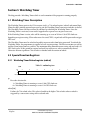
Revision History
Version
Number
Revision
Date
0.0
Jan/16/2006
Jerry Chen Initial Version
0.1
Apr/20/2006
Jerry Chen Update SPI io spec
0.2
Nov/07/2007
2
Author
Ether Lai
Description of Changes
Change EPF011D pin assignment; Change EPF011C pin assignment;
Add Package Information; Add Electrical Characteristics;
Confidential Proprietary
NON-DISCLOSURE AGREEMENT REQUIRED
Explore
User Guide — EPF011ACD_UG V0.2
Section 1 Introduction
1.1
1.2
Overview . . . . . . . . . . . . . . . . . . . . . . . . . . . . . . . . . . . . . . . . . . . . . . . . . . . . . . . . . . . . . . . . 9
Features . . . . . . . . . . . . . . . . . . . . . . . . . . . . . . . . . . . . . . . . . . . . . . . . . . . . . . . . . . . . . . . . . 9
Section 2 Overview
2.1
Block Diagram . . . . . . . . . . . . . . . . . . . . . . . . . . . . . . . . . . . . . . . . . . . . . . . . . . . . . . . . . .11
2.2
2.3
2.4
2.4.1
2.4.2
2.5
Pin Diagram . . . . . . . . . . . . . . . . . . . . . . . . . . . . . . . . . . . . . . . . . . . . . . . . . . . . . . . . . . . .12
Pin Description . . . . . . . . . . . . . . . . . . . . . . . . . . . . . . . . . . . . . . . . . . . . . . . . . . . . . . . . .15
Operation Modes . . . . . . . . . . . . . . . . . . . . . . . . . . . . . . . . . . . . . . . . . . . . . . . . . . . . . . .16
Normal mode (OP_MODE = 0) . . . . . . . . . . . . . . . . . . . . . . . . . . . . . . . . . . . . . . . .16
ICP mode (OP_MODE = 1) . . . . . . . . . . . . . . . . . . . . . . . . . . . . . . . . . . . . . . . . . . . .16
Memory Organization . . . . . . . . . . . . . . . . . . . . . . . . . . . . . . . . . . . . . . . . . . . . . . . . . . .16
2.5.1
2.5.2
2.5.3
2.6
2.6.1
2.6.2
2.6.3
2.6.4
2.6.5
Program Flash Memory. . . . . . . . . . . . . . . . . . . . . . . . . . . . . . . . . . . . . . . . . . . . . . .16
Direct Data RAM . . . . . . . . . . . . . . . . . . . . . . . . . . . . . . . . . . . . . . . . . . . . . . . . . . . . .16
Auxiliary Data RAM . . . . . . . . . . . . . . . . . . . . . . . . . . . . . . . . . . . . . . . . . . . . . . . . . . .17
Special Function Registers (SFR) . . . . . . . . . . . . . . . . . . . . . . . . . . . . . . . . . . . . . . . . .18
Dual Data Pointer (DPTR) . . . . . . . . . . . . . . . . . . . . . . . . . . . . . . . . . . . . . . . . . . . . .19
Accumulator (acc) . . . . . . . . . . . . . . . . . . . . . . . . . . . . . . . . . . . . . . . . . . . . . . . . . . . .19
Program Status Word (psw). . . . . . . . . . . . . . . . . . . . . . . . . . . . . . . . . . . . . . . . . . .19
Stack Pointer (sp). . . . . . . . . . . . . . . . . . . . . . . . . . . . . . . . . . . . . . . . . . . . . . . . . . . . .20
SFR list. . . . . . . . . . . . . . . . . . . . . . . . . . . . . . . . . . . . . . . . . . . . . . . . . . . . . . . . . . . . . . .20
Section 3 Interrupt
3.1
3.2
3.3
3.3.1
3.3.2
3.3.3
Interrupt overview . . . . . . . . . . . . . . . . . . . . . . . . . . . . . . . . . . . . . . . . . . . . . . . . . . . . . .25
Priority level structure . . . . . . . . . . . . . . . . . . . . . . . . . . . . . . . . . . . . . . . . . . . . . . . . . . .26
Special Function Registers. . . . . . . . . . . . . . . . . . . . . . . . . . . . . . . . . . . . . . . . . . . . . . .26
Interrupt Enable register 0 (ien0) . . . . . . . . . . . . . . . . . . . . . . . . . . . . . . . . . . . . .26
Interrupt Enable register 1 (ien1) . . . . . . . . . . . . . . . . . . . . . . . . . . . . . . . . . . . . .27
Interrupt Priority register 0 (ip0) . . . . . . . . . . . . . . . . . . . . . . . . . . . . . . . . . . . . . .28
Section 4 Power Management
4.1
4.1.1
General . . . . . . . . . . . . . . . . . . . . . . . . . . . . . . . . . . . . . . . . . . . . . . . . . . . . . . . . . . . . . . . . .31
Idle Mode . . . . . . . . . . . . . . . . . . . . . . . . . . . . . . . . . . . . . . . . . . . . . . . . . . . . . . . . . . . .31
4.1.2
4.2
4.2.1
Stop Mode . . . . . . . . . . . . . . . . . . . . . . . . . . . . . . . . . . . . . . . . . . . . . . . . . . . . . . . . . . .31
SFR Register Description . . . . . . . . . . . . . . . . . . . . . . . . . . . . . . . . . . . . . . . . . . . . . . . .31
Power Management Control register (pcon). . . . . . . . . . . . . . . . . . . . . . . . . . .31
Explore
Confidential Proprietary
NON-DISCLOSURE AGREEMENT REQUIRED
1
User Guide — EPF011ACD_UG V0.2
4.2.2
Clock Control register (clk_ctl) . . . . . . . . . . . . . . . . . . . . . . . . . . . . . . . . . . . . . . . .32
Section 5 Watchdog Timer
5.1
5.2
5.2.1
5.3
5.3.1
5.3.2
5.3.3
5.3.4
Watchdog Timer Description . . . . . . . . . . . . . . . . . . . . . . . . . . . . . . . . . . . . . . . . . . . .35
Special Function Registers. . . . . . . . . . . . . . . . . . . . . . . . . . . . . . . . . . . . . . . . . . . . . . .35
Watchdog Timer Reload register (wdtrel) . . . . . . . . . . . . . . . . . . . . . . . . . . . . .35
Other Related SFR Register Description . . . . . . . . . . . . . . . . . . . . . . . . . . . . . . . . . .36
Interrupt Enable register 0 (ien0). . . . . . . . . . . . . . . . . . . . . . . . . . . . . . . . . . . . . .36
Interrupt Enable register 1 (ien1). . . . . . . . . . . . . . . . . . . . . . . . . . . . . . . . . . . . . .36
Interrupt Priority register 0 (ip0) . . . . . . . . . . . . . . . . . . . . . . . . . . . . . . . . . . . . . .37
Clock Control register (clk_ctl) . . . . . . . . . . . . . . . . . . . . . . . . . . . . . . . . . . . . . . . .38
Section 6 Flash Control
6.1
6.2
6.2.1
6.2.2
6.2.3
6.2.4
6.3
6.4
6.5
General . . . . . . . . . . . . . . . . . . . . . . . . . . . . . . . . . . . . . . . . . . . . . . . . . . . . . . . . . . . . . . . . .39
SFR Register Description . . . . . . . . . . . . . . . . . . . . . . . . . . . . . . . . . . . . . . . . . . . . . . . .39
Flash Control register (fls_ctl) . . . . . . . . . . . . . . . . . . . . . . . . . . . . . . . . . . . . . . . . .39
Flash Address High register (fls_addh) . . . . . . . . . . . . . . . . . . . . . . . . . . . . . . . .40
Flash Address Low register (fls_addl). . . . . . . . . . . . . . . . . . . . . . . . . . . . . . . . . .40
Flash Data In register (fls_din) . . . . . . . . . . . . . . . . . . . . . . . . . . . . . . . . . . . . . . . .40
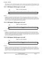
Flash Block Erase Example . . . . . . . . . . . . . . . . . . . . . . . . . . . . . . . . . . . . . . . . . . . . . . .40
Flash Programming Example . . . . . . . . . . . . . . . . . . . . . . . . . . . . . . . . . . . . . . . . . . . .41
On-Chip PROG/ERASE subroutine. . . . . . . . . . . . . . . . . . . . . . . . . . . . . . . . . . . . . . . .41
Section 7 External Interrupts and Port 4
7.1
7.2
7.2.1
7.2.2
7.2.3
7.2.4
7.2.5
7.3
7.3.1
General . . . . . . . . . . . . . . . . . . . . . . . . . . . . . . . . . . . . . . . . . . . . . . . . . . . . . . . . . . . . . . . . .43
SFR Register Description . . . . . . . . . . . . . . . . . . . . . . . . . . . . . . . . . . . . . . . . . . . . . . . .43
Port 4 register (p4) . . . . . . . . . . . . . . . . . . . . . . . . . . . . . . . . . . . . . . . . . . . . . . . . . . .43
Port 4 Direction register (p4d) . . . . . . . . . . . . . . . . . . . . . . . . . . . . . . . . . . . . . . . .43
External Interrupt Polarity register (p4p) . . . . . . . . . . . . . . . . . . . . . . . . . . . . . .44
External Interrupt Enable register (p4e) . . . . . . . . . . . . . . . . . . . . . . . . . . . . . . .44
External Interrupt Flag register (p4f) . . . . . . . . . . . . . . . . . . . . . . . . . . . . . . . . . .44
Other Related SFR Register Description . . . . . . . . . . . . . . . . . . . . . . . . . . . . . . . . . .45
Interrupt Enable register 0 (ien0) . . . . . . . . . . . . . . . . . . . . . . . . . . . . . . . . . . . . .45
Section 8 Key Interrupts and Port 1
8.1
General . . . . . . . . . . . . . . . . . . . . . . . . . . . . . . . . . . . . . . . . . . . . . . . . . . . . . . . . . . . . . . . . .47
2
Confidential Proprietary
NON-DISCLOSURE AGREEMENT REQUIRED
Explore
User Guide — EPF011ACD_UG V0.2
8.2
8.2.1
8.2.2
8.2.3
8.3
8.3.1
SFR Register Description . . . . . . . . . . . . . . . . . . . . . . . . . . . . . . . . . . . . . . . . . . . . . . . .47
Port 1 register (p1) . . . . . . . . . . . . . . . . . . . . . . . . . . . . . . . . . . . . . . . . . . . . . . . . . . .47
Port 1 Direction register (p1d) . . . . . . . . . . . . . . . . . . . . . . . . . . . . . . . . . . . . . . . .47
Key Interrupt Selection register (kbi_en) . . . . . . . . . . . . . . . . . . . . . . . . . . . . . .48
Other Related SFR Register Description . . . . . . . . . . . . . . . . . . . . . . . . . . . . . . . . . .48
Interrupt Enable register 0 (ien0) . . . . . . . . . . . . . . . . . . . . . . . . . . . . . . . . . . . . .48
Section 9 Serial Port
9.1
9.2
9.3
9.3.1
9.3.2
9.3.3
9.3.4
9.4
9.4.1
9.4.2
Serial Interface modes. . . . . . . . . . . . . . . . . . . . . . . . . . . . . . . . . . . . . . . . . . . . . . . . . . .49
Multiprocessor Communication of Serial Port . . . . . . . . . . . . . . . . . . . . . . . . . . . .49
Special Function Registers. . . . . . . . . . . . . . . . . . . . . . . . . . . . . . . . . . . . . . . . . . . . . . .50
Serial Port Control register (S0con). . . . . . . . . . . . . . . . . . . . . . . . . . . . . . . . . . . .50
Serial Port Data Buffer register (s0buf) . . . . . . . . . . . . . . . . . . . . . . . . . . . . . . . .51
Serial Port Baud Rate Reload register low (s0rell) . . . . . . . . . . . . . . . . . . . . . .51
Serial Port Baud Rate Reload register high (s0relh) . . . . . . . . . . . . . . . . . . . .51
Other Related SFR Register Description . . . . . . . . . . . . . . . . . . . . . . . . . . . . . . . . . .52
Interrupt Enable register 0 (ien0) . . . . . . . . . . . . . . . . . . . . . . . . . . . . . . . . . . . . .52
Power Management Control register (pcon). . . . . . . . . . . . . . . . . . . . . . . . . . .53
Section 10 Timer
10.1 General . . . . . . . . . . . . . . . . . . . . . . . . . . . . . . . . . . . . . . . . . . . . . . . . . . . . . . . . . . . . . . . . .55
10.2 SFR Description . . . . . . . . . . . . . . . . . . . . . . . . . . . . . . . . . . . . . . . . . . . . . . . . . . . . . . . . .56
10.2.1
Timer Status register (tim_sta) . . . . . . . . . . . . . . . . . . . . . . . . . . . . . . . . . . . . . . . .56
10.2.2
Timer Selection register (tim_sel) . . . . . . . . . . . . . . . . . . . . . . . . . . . . . . . . . . . . .57
10.2.3
Timer I/O register (tim_io) . . . . . . . . . . . . . . . . . . . . . . . . . . . . . . . . . . . . . . . . . . . .58
10.2.4
Timer Control register (tim_ctl) . . . . . . . . . . . . . . . . . . . . . . . . . . . . . . . . . . . . . . .58
10.2.5
Prescale register (tim_pre) . . . . . . . . . . . . . . . . . . . . . . . . . . . . . . . . . . . . . . . . . . .59
10.2.6
Timer register (timer) . . . . . . . . . . . . . . . . . . . . . . . . . . . . . . . . . . . . . . . . . . . . . . . .60
10.3 Other Related SFR Register Description . . . . . . . . . . . . . . . . . . . . . . . . . . . . . . . . . .60
10.3.1
Interrupt Enable register 0 (ien0) . . . . . . . . . . . . . . . . . . . . . . . . . . . . . . . . . . . . .60
Section 11 PWM
11.1
11.2
General . . . . . . . . . . . . . . . . . . . . . . . . . . . . . . . . . . . . . . . . . . . . . . . . . . . . . . . . . . . . . . . . .63
SFR Register Description . . . . . . . . . . . . . . . . . . . . . . . . . . . . . . . . . . . . . . . . . . . . . . . .63
11.2.1
11.2.2
Explore
PWM Control register (pwm_ctl) . . . . . . . . . . . . . . . . . . . . . . . . . . . . . . . . . . . . . .63
PWM Enable register (pwm_en) . . . . . . . . . . . . . . . . . . . . . . . . . . . . . . . . . . . . . .64
Confidential Proprietary
NON-DISCLOSURE AGREEMENT REQUIRED
3
User Guide — EPF011ACD_UG V0.2
11.2.3
11.2.4
PWM Period Control register (pwm_prd) . . . . . . . . . . . . . . . . . . . . . . . . . . . . . .64
PWM Duty Control register (pwm_dty). . . . . . . . . . . . . . . . . . . . . . . . . . . . . . . .64
Section 12 IIC
12.1 General . . . . . . . . . . . . . . . . . . . . . . . . . . . . . . . . . . . . . . . . . . . . . . . . . . . . . . . . . . . . . . . . .65
12.2 SFR Register Description . . . . . . . . . . . . . . . . . . . . . . . . . . . . . . . . . . . . . . . . . . . . . . . .65
12.2.1
IIC Selection register (iic_sel) . . . . . . . . . . . . . . . . . . . . . . . . . . . . . . . . . . . . . . . . .65
12.3 IIC0/IIC1 SFR Register Set Description . . . . . . . . . . . . . . . . . . . . . . . . . . . . . . . . . . . .66
12.3.1
IIC_M Control register (iicm_ctl) . . . . . . . . . . . . . . . . . . . . . . . . . . . . . . . . . . . . . .66
12.3.2
IIC_M Status register (iicm_sta) . . . . . . . . . . . . . . . . . . . . . . . . . . . . . . . . . . . . . . .67
12.3.3
IIC_M ID register (iicm_id) . . . . . . . . . . . . . . . . . . . . . . . . . . . . . . . . . . . . . . . . . . . .68
12.3.4
IIC_M TX Data register (iicm_td) . . . . . . . . . . . . . . . . . . . . . . . . . . . . . . . . . . . . . .68
12.3.5
IIC_M RX Data register (iicm_rd) . . . . . . . . . . . . . . . . . . . . . . . . . . . . . . . . . . . . . .68
12.3.6
IIC_S Control register (iics_ctl) . . . . . . . . . . . . . . . . . . . . . . . . . . . . . . . . . . . . . . . .69
12.3.7
IIC_S Status register (iics_sta) . . . . . . . . . . . . . . . . . . . . . . . . . . . . . . . . . . . . . . . . .70
12.3.8
IIC_S ID register (iics_id) . . . . . . . . . . . . . . . . . . . . . . . . . . . . . . . . . . . . . . . . . . . . . .71
12.3.9
IIC_S RX Data register (iics_rd) . . . . . . . . . . . . . . . . . . . . . . . . . . . . . . . . . . . . . . . .72
12.3.10 IIC_S ID Mask register (iics_idm) . . . . . . . . . . . . . . . . . . . . . . . . . . . . . . . . . . . . . .72
12.4 Other Related SFR Register Description . . . . . . . . . . . . . . . . . . . . . . . . . . . . . . . . . .72
12.4.1
Interrupt Enable register 0 (ien0) . . . . . . . . . . . . . . . . . . . . . . . . . . . . . . . . . . . . .72
12.4.2
Interrupt Enable register 1 (ien1) . . . . . . . . . . . . . . . . . . . . . . . . . . . . . . . . . . . . .73
Section 13 USB (Universal Serial Bus)
13.1 General . . . . . . . . . . . . . . . . . . . . . . . . . . . . . . . . . . . . . . . . . . . . . . . . . . . . . . . . . . . . . . . . .75
13.2 SFR Register Description . . . . . . . . . . . . . . . . . . . . . . . . . . . . . . . . . . . . . . . . . . . . . . . .75
13.2.1
USB Control register 0 (usb_ctl0). . . . . . . . . . . . . . . . . . . . . . . . . . . . . . . . . . . . . .75
13.2.2
USB Control register 1 (usb_ctl1). . . . . . . . . . . . . . . . . . . . . . . . . . . . . . . . . . . . . .76
13.2.3
USB Control register 2 (usb_ctl2). . . . . . . . . . . . . . . . . . . . . . . . . . . . . . . . . . . . . .77
13.2.4
USB Control register 3 (usb_ctl3). . . . . . . . . . . . . . . . . . . . . . . . . . . . . . . . . . . . . .78
13.2.5
USB Control register 4 (usb_ctl4). . . . . . . . . . . . . . . . . . . . . . . . . . . . . . . . . . . . . .79
13.2.6
USB Control register 5 (usb_ctl5). . . . . . . . . . . . . . . . . . . . . . . . . . . . . . . . . . . . . .80
13.2.7
USB Status register 0 (usb_sta0) . . . . . . . . . . . . . . . . . . . . . . . . . . . . . . . . . . . . . .80
13.2.8
USB Status register 1 (usb_sta1) . . . . . . . . . . . . . . . . . . . . . . . . . . . . . . . . . . . . . .82
13.2.9
USB Status register 2 (usb_sta2) . . . . . . . . . . . . . . . . . . . . . . . . . . . . . . . . . . . . . .83
13.2.10
13.2.11
4
USB Buffer Pointer register (usb_epp) . . . . . . . . . . . . . . . . . . . . . . . . . . . . . . . . .83
USB Endpoint 0 Buffer register (usb_ep0) . . . . . . . . . . . . . . . . . . . . . . . . . . . . .84
Confidential Proprietary
NON-DISCLOSURE AGREEMENT REQUIRED
Explore
User Guide — EPF011ACD_UG V0.2
13.2.12 USB Endpoint 1 Buffer register (usb_ep1) . . . . . . . . . . . . . . . . . . . . . . . . . . . . .84
13.2.13 USB Endpoint 2 Buffer register (usb_ep2) . . . . . . . . . . . . . . . . . . . . . . . . . . . . .84
13.3 Other Related SFR Register Description . . . . . . . . . . . . . . . . . . . . . . . . . . . . . . . . . .85
13.3.1
Interrupt Enable register 0 (ien0) . . . . . . . . . . . . . . . . . . . . . . . . . . . . . . . . . . . . .85
13.3.2
Interrupt Enable register 1 (ien1) . . . . . . . . . . . . . . . . . . . . . . . . . . . . . . . . . . . . .85
Section 14 SPI
14.1
14.2
14.3
14.4
14.4.1
14.4.2
14.4.3
14.4.4
14.5
14.5.1
14.5.2
General . . . . . . . . . . . . . . . . . . . . . . . . . . . . . . . . . . . . . . . . . . . . . . . . . . . . . . . . . . . . . . . . .87
SPI Pins Description . . . . . . . . . . . . . . . . . . . . . . . . . . . . . . . . . . . . . . . . . . . . . . . . . . . . .87
SPI Timing Diagram . . . . . . . . . . . . . . . . . . . . . . . . . . . . . . . . . . . . . . . . . . . . . . . . . . . . .88
SFR Register Description . . . . . . . . . . . . . . . . . . . . . . . . . . . . . . . . . . . . . . . . . . . . . . . .88
SPI Control register 1 (spi_ctl1) . . . . . . . . . . . . . . . . . . . . . . . . . . . . . . . . . . . . . . .89
SPI Control register 2 (spi_ctl2) . . . . . . . . . . . . . . . . . . . . . . . . . . . . . . . . . . . . . . .90
SPI Baud Rate register (spi_br) . . . . . . . . . . . . . . . . . . . . . . . . . . . . . . . . . . . . . . . .91
SPI Data register (spi_d) . . . . . . . . . . . . . . . . . . . . . . . . . . . . . . . . . . . . . . . . . . . . . .92
Other Related SFR Register Description . . . . . . . . . . . . . . . . . . . . . . . . . . . . . . . . . .92
Interrupt Enable register 0 (ien0) . . . . . . . . . . . . . . . . . . . . . . . . . . . . . . . . . . . . .92
Interrupt Enable register 1 (ien1) . . . . . . . . . . . . . . . . . . . . . . . . . . . . . . . . . . . . .93
Section 15 ADC
15.1 General . . . . . . . . . . . . . . . . . . . . . . . . . . . . . . . . . . . . . . . . . . . . . . . . . . . . . . . . . . . . . . . . .95
15.2 SFR Register Description . . . . . . . . . . . . . . . . . . . . . . . . . . . . . . . . . . . . . . . . . . . . . . . .95
15.2.1
ADC Control register 1 (adc_ctl1) . . . . . . . . . . . . . . . . . . . . . . . . . . . . . . . . . . . . .95
15.2.2
ADC Control register 2 (adc_ctl2) . . . . . . . . . . . . . . . . . . . . . . . . . . . . . . . . . . . . .95
15.2.3
ADC Enable register (adc_en) . . . . . . . . . . . . . . . . . . . . . . . . . . . . . . . . . . . . . . . . .96
15.2.4
ADC Data register (adc_d) . . . . . . . . . . . . . . . . . . . . . . . . . . . . . . . . . . . . . . . . . . . .97
15.2.5
ADC I/O register (adc_io) . . . . . . . . . . . . . . . . . . . . . . . . . . . . . . . . . . . . . . . . . . . . .97
15.3 Other Related SFR Register Description . . . . . . . . . . . . . . . . . . . . . . . . . . . . . . . . . .98
15.3.1
Interrupt Enable register 0 (ien0) . . . . . . . . . . . . . . . . . . . . . . . . . . . . . . . . . . . . .98
15.3.2
Interrupt Enable register 1 (ien1) . . . . . . . . . . . . . . . . . . . . . . . . . . . . . . . . . . . . .98
Section 16 CIR (Consumer Infra-Red Remote Decoder)
16.1
16.2
General . . . . . . . . . . . . . . . . . . . . . . . . . . . . . . . . . . . . . . . . . . . . . . . . . . . . . . . . . . . . . . . 101
SFR Register Description . . . . . . . . . . . . . . . . . . . . . . . . . . . . . . . . . . . . . . . . . . . . . . 101
16.2.1
16.2.2
Explore
CIR Control register 1 (cir_ctl1). . . . . . . . . . . . . . . . . . . . . . . . . . . . . . . . . . . . . . 101
CIR Control register 2 (cir_ctl2). . . . . . . . . . . . . . . . . . . . . . . . . . . . . . . . . . . . . . 102
Confidential Proprietary
NON-DISCLOSURE AGREEMENT REQUIRED
5
User Guide — EPF011ACD_UG V0.2
16.2.3
CIR Control register 3 (cir_ctl3). . . . . . . . . . . . . . . . . . . . . . . . . . . . . . . . . . . . . .
16.2.4
CIR Code register (cir_code) . . . . . . . . . . . . . . . . . . . . . . . . . . . . . . . . . . . . . . . .
16.3 Other Related SFR Register Description . . . . . . . . . . . . . . . . . . . . . . . . . . . . . . . .
16.3.1
Interrupt Enable register 0 (ien0) . . . . . . . . . . . . . . . . . . . . . . . . . . . . . . . . . . .
16.3.2
Interrupt Enable register 1 (ien1) . . . . . . . . . . . . . . . . . . . . . . . . . . . . . . . . . . .
102
103
103
103
104
Section 17 I/O Port 0
17.1 General . . . . . . . . . . . . . . . . . . . . . . . . . . . . . . . . . . . . . . . . . . . . . . . . . . . . . . . . . . . . . . .
17.2 SFR Register Description . . . . . . . . . . . . . . . . . . . . . . . . . . . . . . . . . . . . . . . . . . . . . .
17.2.1
Port 0 register (p0) . . . . . . . . . . . . . . . . . . . . . . . . . . . . . . . . . . . . . . . . . . . . . . . . .
17.2.2
Port 0 Direction register (p0d) . . . . . . . . . . . . . . . . . . . . . . . . . . . . . . . . . . . . . .
17.2.3
Port 0 Open Drain Control register (p0od) . . . . . . . . . . . . . . . . . . . . . . . . . . .
105
105
105
105
105
Section 18 I/O Port 2
18.1 General . . . . . . . . . . . . . . . . . . . . . . . . . . . . . . . . . . . . . . . . . . . . . . . . . . . . . . . . . . . . . . .
18.2 SFR Register Description . . . . . . . . . . . . . . . . . . . . . . . . . . . . . . . . . . . . . . . . . . . . . .
18.2.1
Port 2 register (p2) . . . . . . . . . . . . . . . . . . . . . . . . . . . . . . . . . . . . . . . . . . . . . . . . .
18.2.2
Port 2 Direction register (p2d) . . . . . . . . . . . . . . . . . . . . . . . . . . . . . . . . . . . . . .
18.2.3
Port 2 Open Drain Control register (p2od) . . . . . . . . . . . . . . . . . . . . . . . . . . .
107
107
107
107
107
Section 19 I/O Port 3
19.1 General . . . . . . . . . . . . . . . . . . . . . . . . . . . . . . . . . . . . . . . . . . . . . . . . . . . . . . . . . . . . . . . 109
19.2 SFR Register Description . . . . . . . . . . . . . . . . . . . . . . . . . . . . . . . . . . . . . . . . . . . . . . 109
19.2.1
Port 3 register (p3) . . . . . . . . . . . . . . . . . . . . . . . . . . . . . . . . . . . . . . . . . . . . . . . . . 109
Section 20 GPIO
20.1 General . . . . . . . . . . . . . . . . . . . . . . . . . . . . . . . . . . . . . . . . . . . . . . . . . . . . . . . . . . . . . . .
20.2 SFR Register Description for Port 5~9 . . . . . . . . . . . . . . . . . . . . . . . . . . . . . . . . . .
20.2.1
GPIO Port Selection register (gpio_sel) . . . . . . . . . . . . . . . . . . . . . . . . . . . . . .
20.2.2
GPIO IO register (gpio_io) . . . . . . . . . . . . . . . . . . . . . . . . . . . . . . . . . . . . . . . . . .
20.2.3
GPIO Direction register (gpio_d) . . . . . . . . . . . . . . . . . . . . . . . . . . . . . . . . . . . .
20.2.4
GPIO Open Drain Control register (gpio_od) . . . . . . . . . . . . . . . . . . . . . . . .
111
111
111
111
112
112
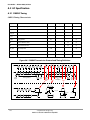
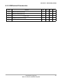
Appendix A Electrical Characteristics
A.1
DC Specification . . . . . . . . . . . . . . . . . . . . . . . . . . . . . . . . . . . . . . . . . . . . . . . . . . . . . . 114
A.2
AC Specification . . . . . . . . . . . . . . . . . . . . . . . . . . . . . . . . . . . . . . . . . . . . . . . . . . . . . . 116
A.2.1
SMBUS Timing . . . . . . . . . . . . . . . . . . . . . . . . . . . . . . . . . . . . . . . . . . . . . . . . . . . . . 116
6
Confidential Proprietary
NON-DISCLOSURE AGREEMENT REQUIRED
Explore
User Guide — EPF011ACD_UG V0.2
A.2.2
USB Electrical Characteristics . . . . . . . . . . . . . . . . . . . . . . . . . . . . . . . . . . . . . . . 117
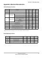
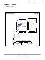
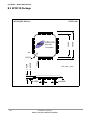
Appendix B Package
B.1
B.2
B.3
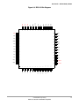
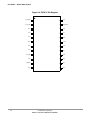
EPF011A Package . . . . . . . . . . . . . . . . . . . . . . . . . . . . . . . . . . . . . . . . . . . . . . . . . . . . . 119
EPF011D Package . . . . . . . . . . . . . . . . . . . . . . . . . . . . . . . . . . . . . . . . . . . . . . . . . . . . . 120
EPF011C Package . . . . . . . . . . . . . . . . . . . . . . . . . . . . . . . . . . . . . . . . . . . . . . . . . . . . . 121
Explore
Confidential Proprietary
NON-DISCLOSURE AGREEMENT REQUIRED
7
User Guide — EPF011ACD_UG V0.2
8
Confidential Proprietary
NON-DISCLOSURE AGREEMENT REQUIRED
Explore
User Guide — EPF011ACD_UG V0.2
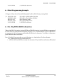
Section 1 Introduction
1.1 Overview
EPF011A/EPF011C/EPF011D is a low cost high performance Micro Controller. The chip integrates 80515
core, 64KB embedded Flash, 256 + 2KB RAM, Timer, Watchdog Timer, Serial Port, 8-bit PWM, SPI, IIC
Slave, IIC Master, 10-bit ADC, USB 1.1, Remote Decoder, Keyboard Interrupt and GPIO in a single chip.
1.2 Features
•
On-chip 80515 core with 64K bytes Flash, 256 bytes Direct RAM and 2K bytes on-chip auxiliary
RAM
•
Fast CPU rate (24Mhz). 41.6 ns for shortest instruction
•
Programmable CPU clocks from 24 Mhz to 500 Khz
•
Programmable crystal start-up cycles from 0 to 4096 cycles
•
Supports Idle mode and Stop mode for power saving.
•
Supports crystal/CPU wake-up from Stop mode
•
Supports In Circuit Flash programming (ICP)
•
Supports 2 external interrupts
•
Supports keyboard interrupt on 4 GPIO pins.
•
On-chip 4 Timers supporting Timer, Pulse Output, Event Counter and Pulse Width Measurement
modes
•
On-chip 15-bit programmable Watchdog Timer
•
On-chip Serial Port which supports Synchronous mode and 8/9-bit UART modes
•
On-chip Serial Peripheral Interface (SPI)
•
On-chip 4 channels of 8-bit PWM with programmable repetition rate
•
On-chip 4 channels of 10-bit ADC
•
On-chip IIC Master and Slave ports with configurable pin outs
•
On-chip USB 1.1 which supports end-pint 0, 1 and 2
•
On-chip Consumer Infra-Red Remote Receiver (CIR) which supports NEC and Phillips RC-5
protocols
•
EPF011A supports 9 General Purpose I/O Ports (total 44 I/O pins). Among them, 6 ports are
open-drain programmable and 2 ports has 20 mA sink capability. All I/O ports are 5V tolerant.
•
EPF011D supports 9 General Purpose I/O Ports (total 31 I/O pins). Among them, 6 ports are
open-drain programmable and 2 ports has 20 mA sink capability. All I/O ports are 5V tolerant.
9
Confidential Proprietary
NON-DISCLOSURE AGREEMENT REQUIRED
User Guide — EPF011ACD_UG V0.2
•
EPF011C supports 7 General Purpose I/O Ports (total 14 I/O pins). Among them, 4 ports are
open-drain programmable and 1 ports has 20 mA sink capability. All I/O ports are 5V tolerant.
•
Timer, SPI and ADC pins can be additional GPIO if the associated function is not enabled
•
On-chip Low Voltage Inhibit (LVI) circuit which provides reliable power up reset and prevent
accidental data loss in Flash
•
Single 24 MHz crystal required
•
Single 3.3V CMOS design
•
64-pin LQFP package (Pb-Free) for EPF011A, 48-pin LQFP package (Pb-Free) for EPF011D,
24-Pin SSOP (Pb-Free) for EPF011C
10
Confidential Proprietary
NON-DISCLOSURE AGREEMENT REQUIRED
User Guide — EPF011ACD_UG V0.2
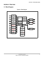
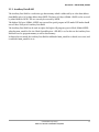
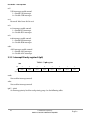
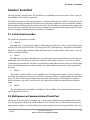
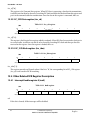
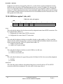
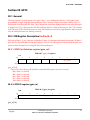
Section 2 Overview
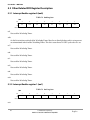
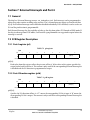
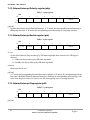
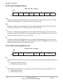
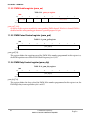
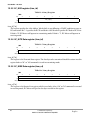
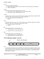
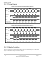
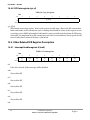
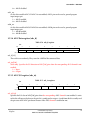
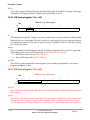
2.1 Block Diagram
Figure 2-1 Block Diagram
Port 0
256B Direct
Data RAM
Port 1
KBI
8051 Core
Port 2
Port 3
IIC
Port 4
Ex. Int.
Port 5
Hi Current
Port 6
Hi Current
Port 7
UART/CIR
Port 8
PWM
Port 9
GPIO
2KB Aux.
Data RAM
LVI
PMU
Timer x 4
SPI
64KB Flash
10-bit ADC x 4
ICP
WDT
UART
USB 1.1
IIC x 2
8-bit PWM x 5
CIR
Confidential Proprietary
NON-DISCLOSURE AGREEMENT REQUIRED
11
User Guide — EPF011ACD_UG V0.2
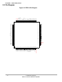
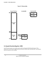
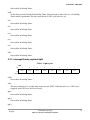
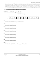
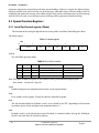
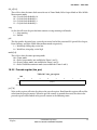
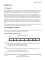
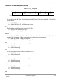
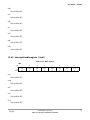
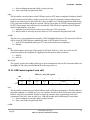
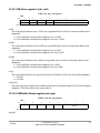
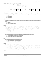
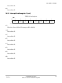
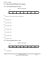
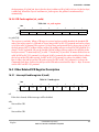
2.2 Pin Diagram
Figure 2-2 EPF011A Pin Diagram
P0[7]
P0[6]
35
34
33
40
P6[0]
41
36
VSS
42
P6[1]
X_IN
43
37
X_OUT
44
P6[2]
VDD
45
38
VSS
46
VDD
SPI_CLK
47
P6[3]
SPI_DO
48
39
P8[1]
32
50
31
P0[4]
P2[3]
51
30
P0[3]
P2[1]
P0[5]
P2[4]
52
29
P0[2]
P2[5]
53
28
P0[1]
P2[6]
54
27
P0[0]
P5[7]
61
20
P5[1]
P7[0]
62
19
P5[0]
P7[1]
63
18
P7[4](CIR)
P4[0]
64
17
VSS
OP_MODE
RSTb
DP
DM
VDDA
ADC[0]
ADC[1]
VSSA
P3[3]
VDD
P3[2]
P3[5]
P3[1]
P3[4]
P3[0]
16
P5[2]
P1[3]
15
60
21
14
P5[3]
P1[2]
13
22
12
59
11
P5[4]
P1[1]
10
23
9
58
8
P5[5]
P1[0]
7
24
6
57
5
P5[6]
TIM[1]
4
25
3
56
2
55
TIM[0]
1
P2[7]
26
P4[1]
12
P8[0]
49
P2[2]
Confidential Proprietary
NON-DISCLOSURE AGREEMENT REQUIRED
User Guide — EPF011ACD_UG V0.2
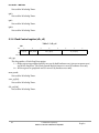
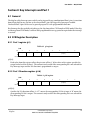
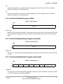
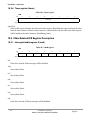
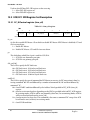
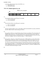
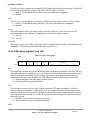
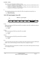
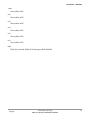
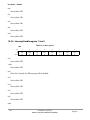
Figure 2-3 EPF011D Pin Diagram
4
5
6
7
8
9
10
11
12
ADC[1]
ADC[0]
VDDA
RSTb
3
ADC[2]
2
ADC[3]
P3[4]
VSSA
P3[1]
VDD
P3[0]
P3[5]
1
25
48
P6[1]
P4[4]
26
47
P6[2]
P4[0]
27
46
P6[3]
P7[1]
28
45
VDD
P7[0]
29
44
VSS
P1[3]
30
43
X_IN
P1[2]
31
42
X_OUT
P1[1]
32
41
VDD
P1[0]
33
40
VSS
TIM[0]
34
39
P8[0]
P2[7]
35
38
P8[1]
P2[6]
36
37
P8[2]
P8[3]
Confidential Proprietary
NON-DISCLOSURE AGREEMENT REQUIRED
24
P6[0]
23
P0[0]
22
P5[7]
21
P5[6]
20
P5[5]
19
P5[4]
18
P5[3]
17
P5[2]
16
P5[1]
15
P5[0]
14
P7[4](CIR)
13
OP_MODE
13
User Guide — EPF011ACD_UG V0.2
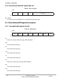
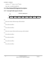
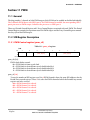
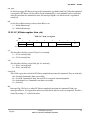
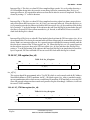
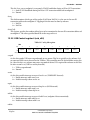
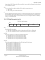
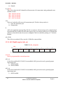
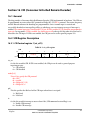
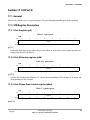
Figure 2-4 EPF011C Pin Diagram
14
P7[0](RXD)
1
24
P1[1]
P7[1](TXD)
2
23
P8[7](PWM)
P4[1]
3
22
P2[1]
P3[0]
4
21
VSS
P3[1]
5
20
VDD
P3[4]
6
19
X_OUT
P3[5]
7
18
X_IN
RSTb
8
17
VSS
OP_MODE
9
16
VDD
P9[0]
10
15
P0[2]
P7[4](CIR)
11
14
P0[1]
P5[0]
12
13
P0[0]
Confidential Proprietary
NON-DISCLOSURE AGREEMENT REQUIRED
User Guide — EPF011ACD_UG V0.2
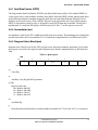
2.3 Pin Description
Unless otherwise stated, unused input pins must be tied to ground, and unused output pins left open.
Table 2-1 Pin Description
Name
In/Out
Buffer Type
OP_MODE
IN
IXDXXP
Chip operation mode.
0: Normal mode
1: ICP (In Circuit Flash Programming) mode
IN/OUT
BDUX8P
External Reset (active low) with on-chip pull-up. When this pin
is asserted low, the chip is totally reset. When the on-chip LVI
circuit is generating a chip reset, a low level will be output
from this pin.
RSTb
Description
X_IN
IN
XTL24P
24 Mhz crystal input
X_OUT
OUT
XTL24P
24 Mhz crystal output
P0[7:0]
IN/OUT
BRXX12P
GPIO port 0 with programmable Open Drain capability.
P1[3:0]
IN/OUT
BRUX8P
GPIO port 1 or Keyboard Interrupt inputs with internal 20KΩ
pull-up to VDD
P2[7:1]
IN/OUT
BRXX8P
GPIO port 2 with programmable Open Drain capability.
P3[5:0]
OD IN/OUT
BRXX8P
Open Drain I/O port 3. P3[5:0] shared with IIC.
P4[4,1:0]
IN/OUT
BRXX8P
GPIO port 4 or External Interrupt inputs
P5[7:0]
IN/OUT
BRXX24P
GPIO port 5 with programmable Open Drain capability
P6[3:0]
IN/OUT
BRXX24P
GPIO port 6 with 20 mA drive
P7[4,1:0]
IN/OUT
BRXX8P
Open Drain I/O port 7. P7[1:0] shared with Serial Port. P7[4]
share with CIR.
P8[7, 3:0]
IN/OUT
BRXX8P
GPIO port 8 with programmable Open Drain capability. P8[7]
and P8[3:0] share with PWM
P9[0]
IN/OUT
BRXX8P
GPIO port 9 with programmable Open Drain capability.
TIM[1:0]
IN/OUT
BRXX8P
Timer In/Out or GPIO
SPI_CLK
IN/OUT
BRXX8P
SPI Clock Out or GPIO
SPI_DO
IN/OUT
BRXX8P
SPI Data In/Out or GPIO
DP
IN/OUT
USB
USB D+ In/Out or GPO
DM
IN/OUT
USB
USB D- In/Out or GPO
ADC[3:0]
IN/OUT
ADC
ADC Inputs or GPIO
VDDA
PWR
-
Analogue VDD (3.3V)
VSSA
PWR
-
Analogue Ground
VDD
PWR
-
Digital VDD (3.3V)
VSS
PWR
-
Digital Ground
Confidential Proprietary
NON-DISCLOSURE AGREEMENT REQUIRED
15
User Guide — EPF011ACD_UG V0.2
2.4 Operation Modes
The chip provides 2 operation modes depending on pin status at OP_MODE pins.
2.4.1 Normal mode (OP_MODE = 0)
The chip is in normal operation. Program starts from $0000 upon reset.
2.4.2 ICP mode (OP_MODE = 1)
The chip is operating the same as in normal mode except that program starts from $F800 upon reset. $F800
is the starting address of ICP boot-loader which downloads the main codes from external and programs
into the Flash from $0000 to $EFFF. Note that if the chip is operating in normal mode but the first byte of
the Flash ($0000) is found erased ($FF), the chip will jump to $F800 to start ICP boot-loader upon reset.
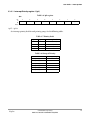
2.5 Memory Organization
There are 3 memory areas in this chip:
1. 64K bytes of Program Flash Memory from $0000 to $FFFF
2. 256 bytes of Direct Data RAM from $00 to $FF
3. 2K bytes of Auxiliary Data RAM from $F800 to $FFFF
2.5.1 Program Flash Memory
The Program Flash Memory is a Flash type program memory which can be erased/programmed on-chip.
So, In Circuit Programming (ICP) is supported. This 64KB Flash memory store the codes to be executed
by the CPU. After reset the CPU starts program execution from location $0000 in normal mode and $F800
in ICP mode. ICP loader should start from $F800. In normal mode, if the content of $0000 is erased, the
program execution will start from location $F800 automatically.
2.5.2 Direct Data RAM
The Direct Data RAM is a read/write type data memory which is addressed by 8-bit short address. This
memory is divided into lower part ($00 ~ $7F) and upper part ($80 ~ $FF).
The lower part contains CPU working registers and bit-addressable memory. The lowest 32 bytes ($00 ~
$1F) form four banks or eight registers (R0~R7). Two bits in the PSW (Program Status Word) select which
bank is in use. The next 16 bytes ($20 ~ $2F) form a block of bit-addressable memory space at bit addresses
$00~$7F. This part of Direct Data RAM can be accessed by either direct or indirect addressing.
The upper part of Direct Data RAM can only be accessed by indirect addressing. Using direct addressing
to access this part of memory will actually access the SFR (Special Function Register) which is not part of
this memory.
16
Confidential Proprietary
NON-DISCLOSURE AGREEMENT REQUIRED
User Guide — EPF011ACD_UG V0.2
2.5.3 Auxiliary Data RAM
The Auxiliary Data RAM is a read/write type data memory which is addressed by an 8-bit short address
from R0/R1 or by a 16-bit long address from DPTR. The lowest 256 bytes ($F800 ~ $F8FF) can be accessed
by either R0/R1 or DPTR. The rest can only be accessed by DPTR.
The highest 256 bytes ($FF00 ~ $FFFF) are reserved for special purpose in ICP mode. ICP loader should
not use these 256 bytes of Auxiliary Data RAM.
The Auxiliary Data RAM can be used to replace the highest 2K program space in Flash ($F800~$FFFF)
when the mem_mode bit (bit-6 in Clock Control Register - SFR $FF) is set. In this case the Auxiliary Data
RAM will serve as program memory as well as data memory.
In External Access mode, the Auxiliary Data RAM is inhibited if mem_mode bit is cleared (reset state) and
is enabled if mem_mode bit is set.
Confidential Proprietary
NON-DISCLOSURE AGREEMENT REQUIRED
17
User Guide — EPF011ACD_UG V0.2
Figure 2-5 Memory Map
Program Flash Mem
Direct Data RAM
Aux Data RAM
$00
$7F
$80
$FF
$0000
Direct/Indirect
(128B)
Indirect
(128B)
User Program
(60KB)
$EFFF
$F000
ICP Loader
(4KB)
$0000/F800
$00FF/F8FF
$F900
(256B)
(1.75KB)
$FFFF
$FFFF
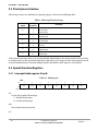
2.6 Special Function Registers (SFR)
Special function registers are on-chip registers which are designed with dedicated functions. These
registers are accessed by direct addressing to the Internal Data RAM space from $80 to $FF. So a maximum
total of 128 registers can be available.
18
Confidential Proprietary
NON-DISCLOSURE AGREEMENT REQUIRED
User Guide — EPF011ACD_UG V0.2
2.6.1 Dual Data Pointer (DPTR)
The chip provides dual Data Pointer (DPTR) to facilitate block moves of data. The standard DPTR is a
16-bit register that is used to address Auxiliary Data RAM. With dual DPTR scheme, moving multi bytes
of data from one location to another or moving multi bytes of codes from Program Memory to Data
Memory can be much easier. Of the 2 DPTRs, only one can be selected for any activity which requires
DPTR. A data pointer switch bit (dps) is designed to switch DPTR from one to another. The dps bit is
implemented as a single bit SFR register (bit-0) located at $92. Bit 1~7 in this register is not used.
2.6.2 Accumulator (acc)
Accumulator is used by the CPU to hold operand for most instructions. The mnemonics for accumulator
specific instructions refer to accumulator as A. Accumulator is implemented as an SFR located at $E0.
2.6.3 Program Status Word (psw)
Program Status Word is used by the CPU to report status after most arithmetic operations. 2 bits inside
this register are used to select register banks. Program Status Word is implemented as an SFR located at
$D0.
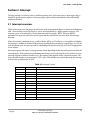
Table 2-2 psw register
$D0
bit
R
W
Reset:
7
6
5
cy
ac
-
-
-
-
4
3
rs[1:0]
0
0
2
1
0
ov
-
p
-
-
-
cy:
Carry flag.
ac:
Auxiliary Carry flag for BCD operations.
rs[1:0]:
Register bank select.
00 = Bank 0, $00~$07
01 = Bank 1, $08~$0F
10 = Bank 2, $10~$17
11 = Bank 3, $08~$1F
ov:
Overflow flag
p:
Parity flag affected by hardware to indicate odd/even number of "1" bits in the ACC, i.e. even parity.
Confidential Proprietary
NON-DISCLOSURE AGREEMENT REQUIRED
19
User Guide — EPF011ACD_UG V0.2
2.6.4 Stack Pointer (sp)
Stack Pointer is a 1-byte register initialized to $07 after reset. This register is incremented before PUSH and
CALL instructions, causing the stack to begin at location $08. Stack Pointer is implemented as an SFR
located at $81.
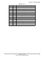
2.6.5 SFR list
The following table is a complete list for each SFR register:
Table 2-3 SFR list
20
Register
Location
Description
p0
$80
I/O Port 0
sp
$81
Stack Pointer
dpl
$82
DPTR0 low byte
dph
$83
DPTR0 high byte
dpl1
$84
DPTR1 low byte
dph1
$85
DPTR1 high byte
wdtrel
$86
Watchdog Timer Reload Register
pcon
$87
Power Management Control Register
tim_sta
$88
Timer Status Register
tim_sel
$89
Timer Selection Register
tim_io
$8A
Timer I/O Register
tim_ctl
$8B
Timer Control Register
tim_pre
$8C
Timer Prescale Register
timer
$8D
Timer Register
adc_ctl1
$8E
ADC Control Register 1
adc_ctl2
$8F
ADC Control Register 2
p1
$90
I/O Port 1
adc_io
$91
ADC I/O Register
dps
$92
DPTR switch
-
$93
-
-
$94
-
-
$95
-
-
$96
-
adc_d
$97
ADC Data Register
s0con
$98
Serial Port Control Register
s0buf
$99
Serial Port Data Buffer Register
gpio_io
$9A
GPIO I/O Register
gpio_d
$9B
GPIO Direction Control Register
gpio_od
$9C
GPIO Open Drain Control Register
-
$9D
-
Confidential Proprietary
NON-DISCLOSURE AGREEMENT REQUIRED
User Guide — EPF011ACD_UG V0.2
Table 2-3 SFR list
Register
Location
Description
-
$9E
-
-
$9F
-
p2
$A0
I/O Port 2
gpio_sel
$A1
GPIO I/O Port Selection Register
-
$A2
-
-
$A3
-
cir_ctl1
$A4
CIR Control Register 1
cir_clt2
$A5
CIR Control Register 2
cir_clt3
$A6
CIR Control Register 3
cir_code
$A7
CIR Code Register
ien0
$A8
Interrupt Enable Register 0
ip0
$A9
Interrupt Priority Register 0
s0rell
$AA
Serial Port Baud Rate Reload Register low byte
adc_en
$AB
ADC Enable Register
pwm_ctl
$AC
PWM Control Register
pwm_en
$AD
PWM Enable Register
pwm_prd
$AE
PWM Period Control Register
pwm_dty
$AF
PWM Duty Control Register
p3
$B0
I/O Port 3
iics_ctl
$B1
IIC Slave Control Register
iics_sta
$B2
IIC Slave Status Register
iics_id
$B3
IIC Slave ID Register
iics_td
$B4
IIC Slave Tx Data Register
iics_rd
$B5
IIC Slave Rx Data Register
iics_idm
$B6
IIC Slave ID Mask Register
iicm_ctl
$B7
IIC Master Control Register
ien1
$B8
Interrupt Enable Register 1
ip1
$B9
Interrupt Priority Register 1
s0relh
$BA
Serial Port Baud Rate Reload Register high byte
iic_sel
$BB
IIC Selection Register
iicm_sta
$BC
IIC Master Status Register
iicm_id
$BD
IIC Master ID Register
iicm_td
$BE
IIC Master Tx Data Register
iicm_rd
$BF
IIC Master Rx Data Register
spi_ctl1
$C0
SPI Control Register 1
spi_ctl2
$C1
SPI Control Register 2
spi_br
$C2
SPI Baud Rate Register
spi_d
$C3
SPI Data Register
-
$C4
-
-
$C5
-
-
$C6
-
Confidential Proprietary
NON-DISCLOSURE AGREEMENT REQUIRED
21
User Guide — EPF011ACD_UG V0.2
Table 2-3 SFR list
22
Register
Location
Description
-
$C7
-
p0od
$C8
I/O Port 0 Open Drain Control Register
-
$C9
-
-
$CA
-
-
$CB
-
-
$CC
-
-
$CD
-
-
$CE
-
-
$CF
-
psw
$D0
Program Status Word
-
$D1
-
-
$D2
-
-
$D3
-
-
$D4
-
-
$D5
-
-
$D6
-
-
$D7
-
p2od
$D8
I/O Port 2 Open Drain Control Register
-
$D9
-
-
$DA
-
-
$DB
-
-
$DC
-
-
$DD
-
-
$DE
-
-
$DF
-
acc
$E0
Accumulator
-
$E1
-
-
$E2
-
-
$E3
-
usb_ctl0
$E4
USB Control Register 0
usb_ctl1
$E5
USB Control Register 1
usb_ctl2
$E6
USB Control Register 2
usb_ctl3
$E7
USB Control Register 3
usb_ctl4
$E8
USB Control Register 4
usb_ctl5
$E9
USB Control Register 5
usb_sta0
$EA
USB Status Register 0
usb_sta1
$EB
USB Status Register 1
usb_sta2
$EC
USB Status Register 2
usb_ep0
$ED
USB End Point 0 Data Register
usb_ep1
$EE
USB End Point 1 Data Register
Confidential Proprietary
NON-DISCLOSURE AGREEMENT REQUIRED
User Guide — EPF011ACD_UG V0.2
Table 2-3 SFR list
Register
Location
Description
usb_ep2
$EF
USB End Point 2 Data Register
b
$F0
B register, used for MULAB instruction
kbi_en
$F1
Key Interrupt Enable Register
p4
$F2
I/O Port 4
p4d
$F3
I/O Port 4 Direction Register
p4p
$F4
External Interrupt Polarity Register
p4e
$F5
External Interrupt Enable Register
p4f
$F6
External Interrupt Flag Register
usb_epp
$F7
USB End Point Buffer Pointer
fls_ctl
$F8
Flash Control Register
fls_addh
$F9
Flash Address Register high byte
fls_addl
$FA
Flash Address Register low byte
fls_din
$FB
Flash Data In Register
p0d
$FC
I/O Port 0 Direction Register
p1d
$FD
I/O Port 1 Direction Register
p2d
$FE
I/O Port 2 Direction Register
clk_ctl
$FF
Clock Control Register
Confidential Proprietary
NON-DISCLOSURE AGREEMENT REQUIRED
23
User Guide — EPF011ACD_UG V0.2
24
Confidential Proprietary
NON-DISCLOSURE AGREEMENT REQUIRED
User Guide — Interrupt V0.2
Section 3 Interrupt
The chip provides 12 interrupt sources with four priority levels. Each source has its own request flag(s)
located in special function registers. Interrupt requests generated by each module can be individually
enabled or disabled.
3.1 Interrupt overview
When an interrupt occur, the processor will vector to the predetermined address as shown in the following
table. Once interrupt service has begun, it can be interrupted only by a higher priority interrupt. The
interrupt service is terminated by a return from interrupt instruction, "RETI". When an RETI is
performed, the processor will return to the instruction that would have been next when the interrupt
occurred.
When the interrupt condition occurs, usually a flag bit will be set. The flag bit is set regardless of whether
the interrupt is enabled or disabled. If the interrupt is enabled, then an interrupt request flag is set. ON the
next instruction cycle, the interrupt will be acknowledged by hardware forcing an LCALL to appropriate
vector address.
Interrupt response will require a varying amount of time depending on the state of the processor when the
interrupt occurs. If the processor is performing an interrupt service with equal or greater priority, the new
interrupt will not be invoked. In other cases, the response time depends on the current instruction. The
fastest possible response to an interrupt is 7 CPU cycles. This includes one cycle for detecting the interrupt
and six cycles to perform the LCALL.
Table 3-1 Interrupt Vectors
Explore
Interrupt #
Vector Address
1
$0003
External Interrupts
Interrupts
2
$000B
Timer Interrupt
3
$0013
Key Interrupt
4
$001B
reserved
5
$0023
Serial Port Interrupt
6
$002B
reserved
7
$0043
ADC Interrupt
8
$004B
IIC0 Interrupts
9
$0053
IIC1 Interrupts
10
$005B
reserved
11
$0063
USB Interrupts
12
$006B
CIR Interrupt
13
$0083
SPI Interrupt
Confidential Proprietary
NON-DISCLOSURE AGREEMENT REQUIRED
25
User Guide —Interrupt V0.2
3.2 Priority level structure
All interrupt sources are combined in 6 priority groups as shown in the following table:
Table 3-2 Interrupt Priority Groups
Priority
Group
Polling
Sequence
0
1
2
3
External Interrupts
SPI Interrupts
ADC Interrupt
1
4
5
Timer Interrupts
IIC0 Interrupts
2
6
7
Key Interrupt
IIC1 Interrupts
3
8
9
reserved
reserved
4
10
11
Serial Port Interrupts
USB Interrupts
5
12
13
reserved
CIR Interrupt
Interrupts
Each group of interrupt sources can be programmed individually to one of four priority level by setting
or clearing one bit in the special function register ip0 and in ip1. If requests of the same priority level are
received simultaneously, an internal polling sequence determines which request is serviced first.
3.3 Special Function Registers
3.3.1 Interrupt Enable register 0 (ien0)
Table 3-3 ien0 register
$A8
bit
R
W
Reset:
7
6
5
4
3
2
1
0
eal
wdt
ex7
es0
et1
ex1
et0
ex0
0
0
0
0
0
0
0
0
eal:
Set this bit to enable all interrupts.
1 = Enable all interrupts
0 = Disable all interrupts
wdt:
Not used for interrupt control.
ex7:
26
Confidential Proprietary
NON-DISCLOSURE AGREEMENT REQUIRED
Explore
User Guide — Interrupt V0.2
Reserved. Must leave this bit as 0.
es0:
Serial Port interrupts enable control.
1 = Enable Serial Port interrupts
0 = Disable Serial Port interrupts
et1:
Not used.
ex1:
Key interrupt enable control.
1 = Enable Key interrupt
0 = Disable Key interrupt
et0:
Timer interrupts enable control.
1 = Enable Timer interrupts
0 = Disable Timer interrupts
ex0:
External interrupts enable control.
1 = Enable External interrupts
0 = Disable External interrupts
3.3.2 Interrupt Enable register 1 (ien1)
Table 3-4 ien1 register
$B8
bit
R
W
Reset:
7
6
5
4
3
2
1
0
ex8
swdt
ex6
ex5
ex4
ex3
ex2
eadc
0
0
0
0
0
0
0
0
ex8:
SPI interrupt enable control.
1 = Enable SPI interrupts
0 = Disable SPI interrupts
swdt:
Not used for interrupt control
ex6:
CIR interrupt enable control.
1 = Enable CIR interrupts
0 = Disable CIR interrupts
Explore
Confidential Proprietary
NON-DISCLOSURE AGREEMENT REQUIRED
27
User Guide —Interrupt V0.2
ex5:
USB interrupts enable control.
1 = Enable USB interrupts
0 = Disable USB interrupts
ex4:
Reserved. Must leave this bit as 0.
ex3:
IIC1 interrupts enable control.
1 = Enable IIC1 interrupts
0 = Disable IIC1 interrupts
ex2:
IIC0 interrupts enable control.
1 = Enable IIC0 interrupts
0 = Disable IIC0 interrupts
eadc:
ADC interrupts enable control.
1 = Enable ADC interrupts
0 = Disable ADC interrupts
3.3.3 Interrupt Priority register 0 (ip0)
Table 3-5 ip0 register
$A9
bit
R
W
Reset:
7
6
5
4
3
2
1
0
owds
wdts
ip0.5
ip0.4
ip0.3
ip0.2
ip0.1
ip0.0
0
0
0
0
0
0
0
0
owds:
Not used for interrupt control.
wdts:
Not used for interrupt control.
ip0.5 ~ ip0.0:
Set interrupt priority level for each priority group. See the following tables.
28
Confidential Proprietary
NON-DISCLOSURE AGREEMENT REQUIRED
Explore
User Guide — Interrupt V0.2
3.3.3.1 Interrupt Priority register 1 (ip1)
Table 3-6 ip1 register
$B9
bit
R
W
Reset:
7
6
5
4
3
2
1
0
-
-
ip1.5
ip1.4
ip1.3
ip1.2
ip1.1
ip1.0
0
0
0
0
0
0
0
0
ip1.5 ~ ip1.0:
Set interrupt priority level for each priority group. See the following tables.
Table 3-7 Priority levels
ip1.x
ip0.x
Priority level
0
0
Level0(lowest)
0
1
Level1
1
0
Level2
1
1
Level3
Table 3-8 Group of Priority
Explore
Bit
Priority Group
ip1.0, ip0.0
0
ip1.1, ip0.1
1
ip1.2, ip0.2
2
ip1.3, ip0.3
3
ip1.4, ip0.4
4
ip1.5, ip0.5
5
Confidential Proprietary
NON-DISCLOSURE AGREEMENT REQUIRED
29
User Guide —Interrupt V0.2
30
Confidential Proprietary
NON-DISCLOSURE AGREEMENT REQUIRED
Explore
User Guide — PMU V0.2
Section 4 Power Management
4.1 General
The chip provides various power saving modes for low power operation. In normal operation, CPU clock
rate can be programmed to achieve best trade-off between power consumption and CPU speed. In Idle
mode, CPU clock is stopped while peripheral clock is running. In Stop mode, all the clocks are stopped to
achieve lowest power consumption.
4.1.1 Idle Mode
In Idle mode, the CPU clock is stopped. Power consumption drops because CPU is not active. Peripheral
clock are kept running. In this mode, CPU can be waken up by any interrupt or reset.
4.1.2 Stop Mode
In Stop mode, all the clocks including the CPU clock and Peripheral clock are stopped to achieve lowest
power consumption. In this mode, CPU can only be waken up by External Interrupts, Keyboard Interrupt,
SMBUS Interrupt or reset.
If the chip is waken up from STOP mode, it will wait for a programmable start up period to expire before
CPU resumes operation.
4.2 SFR Register Description
4.2.1 Power Management Control register (pcon)
Table 4-1 pcon register
$87
bit
R
W
Reset:
7
6
5
4
3
2
1
0
smod
-
-
-
gf1
gf0
stop
idle
0
-
-
-
0
0
0
0
smod:
Not used for Power Management.
gf1:
Not used for Power Management.
gf0:
Not used for Power Management.
stop:
Stop mode control bit. Set this bit by software to enter Stop mode. This bit is always read as 0.
Explore
Confidential Proprietary
NON-DISCLOSURE AGREEMENT REQUIRED
31
User Guide —PMU V0.2
stop:
Idle mode control bit. Set this bit by software to enter Idle mode. This bit is always read as 0.
4.2.2 Clock Control register (clk_ctl)
Table 4-2 clk_ctl
$FF
bit
R
W
Reset:
7
6
5
wdt_opt
mem_mode
0
0
4
3
2
start_up[2:0]
1
1
1
0
clk_rate[2:0]
1
0
0
1
wdt_opt:
This bit provides a Watch Dog Reset option.
1 = All the registers in peripheral and I/O are reset by both hardware reset (pin reset or power reset)
and Watch Dog Reset. The Clock Control Register however is reset by hardware reset only.
0 = All the registers in peripheral and I/O are reset by hardware reset only.
mem_mode:
Set this bit to make the Auxiliary Data RAM to replace the highest 2K program space in Flash
($F800~$FFFF). In this case the Auxiliary Data RAM will serve as program memory as well as data
memory
1 = Switch the highest 2K program space from Flash to the Auxiliary Data RAM
0 = Keep the highest 2K program space in Flash.
start_up[2:0]:
When the chip is powered up or waken up from Stop mode, it will wait for a programmable start up
period to expire before CPU resumes operation. This register specifies the start up period.
000 = 0 crystal clocks
001 = 64 crystal clocks
010 = 128 crystal clocks
011 = 256 crystal clocks
100 = 512 crystal clocks
101 = 1024 crystal clocks
110 = 2048 crystal clocks
111 = 4096 crystal clocks
clk_rate[2:0]:
This register specifies the CPU clock rate.
000 = CPU Clock rate = Crystal Clock rate
001 = CPU Clock rate = Crystal Clock rate/2
010 = CPU Clock rate = Crystal Clock rate/4
011 = CPU Clock rate = Crystal Clock rate/8
100 = CPU Clock rate = Crystal Clock rate/16
101 = CPU Clock rate = Crystal Clock rate/32
110 = CPU Clock rate = Crystal Clock rate/64
32
Confidential Proprietary
NON-DISCLOSURE AGREEMENT REQUIRED
Explore
User Guide — PMU V0.2
111 = CPU Clock rate = Crystal Clock rate/128
Explore
Confidential Proprietary
NON-DISCLOSURE AGREEMENT REQUIRED
33
User Guide —PMU V0.2
34
Confidential Proprietary
NON-DISCLOSURE AGREEMENT REQUIRED
Explore
User Guide — WDT V0.2
Section 5 Watchdog Timer
The chip provide a Watchdog Timer which is used to monitor if the program is running properly.
5.1 Watchdog Timer Description
The Watchdog Timer consists of a 15-bit counter (wdtc), a 7-bit reload register (wdtrel) and control logic.
When the chip is initially powered up or reset by pin, the Watchdog Timer is not active and wdtc is cleared.
The Watchdog Timer can then activated by software by refreshing the Watchdog Timer. Once the
Watchdog Timer is activated, it can not be stopped unless a power reset or pin reset occurs.
If the Watchdog Timer is active, wdtc will be counting up at a rate of 1/24 or 1/384 CPU clock rate
depending on register setting. When wdtc enters the state $7FFC, a signal wdts will be generated to trigger
CPU reset.
The Watchdog Timer must be refreshed regularly to prevent wdts from being generated. To refresh the
Watchdog Timer, the programmer is required to issue two instructions. The first instruction sets wdt bit
and the second instruction sets swdt bit. The maximum delay allowed between setting wdt and swdt is 12
CPU clock cycles. If this period has expired and swdt has not been set, wdt is automatically cleared.
Otherwise the most significant 7 bits of wdtc is reloaded with the content of wdtrel.
5.2 Special Function Registers
5.2.1 Watchdog Timer Reload register (wdtrel)
Table 5-1 wdtrel register
$86
bit
R
W
Reset:
7
6
5
4
ps
0
3
2
1
0
0
0
0
wdtrel[6:0]
0
0
0
0
ps:
Prescaler selection bit.
1 = Watchdog Timer is counting at a rate 1/384 CPU clock rate
0 = Watchdog Timer is counting at a rate 1/24 CPU clock rate
wdtrel[6:0]:
Defines the 7-bit reload value. This value is loaded to the higher 7 bits of wdtc when a refresh is
triggered by a consecutive setting of bits wdt and swdt.
Explore
Confidential Proprietary
NON-DISCLOSURE AGREEMENT REQUIRED
35
User Guide —WDT V0.2
5.3 Other Related SFR Register Description
5.3.1 Interrupt Enable register 0 (ien0)
Table 5-2 ien0 register
$A8
bit
R
W
Reset:
7
6
5
4
3
2
1
0
eal
wdt
ex7
es0
et1
ex1
et0
ex0
0
0
0
0
0
0
0
0
eal:
Not used for Watchdog Timer.
wdt:
Set this bit to initiate a refresh of the Watchdog Timer. Must be set directly before swdt is set to prevent
an unintentional refresh of the Watchdog Timer. This bit is auto cleared 12 CPU cycles after it is set.
ex7:
Not used for Watchdog Timer.
es0:
Not used for Watchdog Timer.
et1:
Not used for Watchdog Timer.
ex1:
Not used for Watchdog Timer.
et0:
Not used for Watchdog Timer.
ex0:
Not used for Watchdog Timer.
5.3.2 Interrupt Enable register 1 (ien1)
Table 5-3 ien1 register
$B8
bit
R
W
Reset:
7
6
5
4
3
2
1
0
ex8
swdt
ex6
ex5
ex4
ex3
ex2
eadc
0
0
0
0
0
0
0
0
ex8:
36
Confidential Proprietary
NON-DISCLOSURE AGREEMENT REQUIRED
Explore
User Guide — WDT V0.2
Not used for Watchdog Timer.
swdt:
Set this bit to activate/refresh the Watchdog Timer. When directly set after wdt is set, a Watchdog
Timer refresh is performed. This bit is auto cleared 12 CPU cycles after it is set.
ex6:
Not used for Watchdog Timer.
ex5:
Not used for Watchdog Timer.
ex4:
Not used for Watchdog Timer.
ex3:
Not used for Watchdog Timer.
ex2:
Not used for Watchdog Timer.
eadc:
Not used for Watchdog Timer.
5.3.3 Interrupt Priority register 0 (ip0)
Table 5-4 ip0 register
$A9
bit
R
W
Reset:
7
6
5
4
3
2
1
0
owds
wdts
ip0.5
ip0.4
ip0.3
ip0.2
ip0.1
ip0.0
0
0
0
0
0
0
0
0
owds:
Not used for Watchdog Timer.
wdts:
This bit is read only. It is set when wdtc enters the state $7FFC. When this bit is set, a CPU reset is
triggered. After CPU reset, this bit is cleared.
ip0.5:
Not used for Watchdog Timer.
ip0.4:
Not used for Watchdog Timer.
ip0.3:
Explore
Confidential Proprietary
NON-DISCLOSURE AGREEMENT REQUIRED
37
User Guide —WDT V0.2
Not used for Watchdog Timer.
ip0.2:
Not used for Watchdog Timer.
ip0.1:
Not used for Watchdog Timer.
ip0.0:
Not used for Watchdog Timer.
5.3.4 Clock Control register (clk_ctl)
Table 5-5 clk_ctl
$FF
bit
R
W
Reset:
7
6
5
wdt_opt
mem_mode
0
0
4
3
2
start_up[2:0]
1
1
1
0
clk_rate[2:0]
1
0
0
1
wdt_opt:
This bit provides a Watch Dog Reset option.
1 = All the registers in peripheral and I/O are reset by both hardware reset (pin reset or power reset)
and Watch Dog Reset. The Clock Control Register however is reset by hardware reset only.
0 = All the registers in peripheral and I/O are reset by hardware reset only.
mem_mode:
Not used for Watchdog Timer.
start_up[2:0]:
Not used for Watchdog Timer.
clk_rate[2:0]:
Not used for Watchdog Timer.
38
Confidential Proprietary
NON-DISCLOSURE AGREEMENT REQUIRED
Explore
User Guide — FLS_CTL V0.2
Section 6 Flash Control
6.1 General
The chip provides on-chip flash memory as program storage. The on-chip flash memory can be
programmed or erased by codes reside in the same flash memory. On-chip PROG and ERASE subroutines
and a set of control registers are provided for this purpose.
6.2 SFR Register Description
6.2.1 Flash Control register (fls_ctl)
Table 6-1 fls_ctl register
$F8
bit
R
W
Reset:
7
6
5
4
3
2
1
0
icp
prot
xe
ye
erase
mas1
prog
nvstr
0
0
0
0
0
0
0
0
icp:
This bit is used by the on-chip PROGRM/ERASE subroutine. It is set at the start of the subroutines and
cleared at the end of the subroutines. When this bit toggles, all the other bit in fls_con register are
cleared.
prot:
This bit needs to be set before the erase and prog bits can be set.
xe:
Set to enable X address of the flash memory.
ye:
Set to enable Y address of the flash memory.
erase:
Set this bit after writing $AA to fls_din register will perform flash erase. This bit is used in conjunction
with nvstr bit to control flash erase procedure.
mas1:
Set this bit after writing $55 to fls_din register will put the flash memory in master erase mode.
Otherwise the flash memory will stay in block erase mode if erase operation is performed.
prog:
This bit is used in conjunction with nvstr bit to control flash program procedure.
nvstr:
Explore
Confidential Proprietary
NON-DISCLOSURE AGREEMENT REQUIRED
39
User Guide —FLS_CTL V0.2
This bit is used in conjunction with erase bit and prog bit to control flash erase/program procedure.
6.2.2 Flash Address High register (fls_addh)
Table 6-2 fls_addh register
$F9
bit
R
W
Reset:
7
6
5
4
3
2
1
0
0
0
0
fls_addh[7:0]
0
0
0
0
0
fls_addh[7:0]:
This register holds the higher 8-bit of the flash memory address for erase/program operation.
6.2.3 Flash Address Low register (fls_addl)
Table 6-3 fls_addl register
$FA
bit
R
W
Reset:
7
6
5
4
3
2
1
0
0
0
0
0
fls_addl[7:0]
0
0
0
0
fls_addl[7:0]:
This register holds the lower 8-bit of the flash memory address for erase/program operation.
6.2.4 Flash Data In register (fls_din)
Table 6-4 fls_din register
$FB
bit
R
W
Reset:
7
6
5
4
3
2
1
0
0
0
0
0
fls_din[7:0]
0
0
0
0
fls_din[7:0]:
This register holds the 8-bit data to be programmed into the flash memory during the flash
programming procedure.
6.3 Flash Block Erase Example
// Erase a 512-byte block starting $F800
J0: MOV $F9, #$F8
MOV $FA, #$00
40
// fls_addh <= Flash Address high byte
// fls_addl <= Flash Address low byte
Confidential Proprietary
NON-DISCLOSURE AGREEMENT REQUIRED
Explore
User Guide — FLS_CTL V0.2
LCALL $FF80
// Call ERASE subroutine
6.4 Flash Programming Example
// Program 16 bytes data in Internal RAM pointed by R1 to Flash Memory starting $f800
J1: MOV $F9, #$F8
MOV $FA, #$00
MOV R3, #16
MOV R1, #$40
LCALL $FFC0
// fls_addh <= Flash Address high byte
// fls_addl <= Flash Address low byte
// R3 as data byte count
// R1 as data buffer pointer
// Call PROG subroutine
6.5 On-Chip PROG/ERASE subroutine
The on-chip PROG subroutine (starting $FFC0) and ERASE subroutine (starting $FF80) are programmed
to the last 128 bytes of the flash memory before shipping. User is recommended to use these 2 subroutines
to program/erase the flash memory and should not erase these 2 subroutines. To call these 2 subroutines
please follow the notes stated below:
Note: 1. Disable all interrupt and reset watch dog timer to > 20ms before call to the subroutine.
2. fls_addh register must be written before call.
3. ACC, R1, R2, R3 and DPTR are used by the subroutines. They should be saved before call if needed.
Explore
Confidential Proprietary
NON-DISCLOSURE AGREEMENT REQUIRED
41
User Guide —FLS_CTL V0.2
42
Confidential Proprietary
NON-DISCLOSURE AGREEMENT REQUIRED
Explore
User Guide — EXT_INT V0.2
Section 7 External Interrupts and Port 4
7.1 General
The chip has 2 External Interrupt sources: ext_int0 and ext_int1. Each interrupt can be programmed as
either rising edge sensitive or falling edge sensitive. The 2 external interrupt inputs are shared with Port
4[1:0]. Each external interrupt can be enabled or disabled individually. If it is disabled, it can be used as an
I/O and the pin direction is programmable.
Each External Interrupt has the capability of wake up the chip from either STOP mode or IDLE mode. If
the chip is waken up from STOP mode, it will wait for a programmable start up period to expire before the
interrupt is serviced.
7.2 SFR Register Description
7.2.1 Port 4 register (p4)
Table 7-1 p4 register
$F2
bit
R
W
Reset:
7
6
5
4
3
2
-
-
-
-
-
-
-
-
-
0
0
0
1
0
p4[1:0]
0
0
p4[1:0]:
Read value from this register reflects the pin state of Port 4. Write value to this register specifies the
output level of each bit in Port 4. The content is only useful if the corresponding External Interrupt bit
is disabled and the I/O direction is programmed as output.
7.2.2 Port 4 Direction register (p4d)
Table 7-2 p4d register
$F3
bit
R
W
Reset:
7
6
5
4
3
2
-
-
-
-
-
-
-
-
-
1
1
1
1
0
p4d[1:0]
1
1
p4d[1:0]:
Specifies the I/O direction of Port 4. A "1" means the corresponding I/O bit is input. A "0" means the
corresponding I/O bit is output. The content is only useful if the corresponding External Interrupt bit
is disabled.
Explore
Confidential Proprietary
NON-DISCLOSURE AGREEMENT REQUIRED
43
User Guide —EXT_INT V0.2
7.2.3 External Interrupt Polarity register (p4p)
Table 7-3 p4p register
$F4
bit
R
W
Reset:
7
6
5
4
3
2
-
-
-
-
-
-
-
-
-
0
0
0
1
0
p4p[1:0]
0
0
p4p[1:0]:
Specifies the polarity of each External Interrupt. A "1" means the corresponding external interrupt is
falling edge sensitive. A "0" means the corresponding external interrupt is rising edge sensitive.
7.2.4 External Interrupt Enable register (p4e)
Table 7-4 p4e register
$F5
bit
R
W
Reset:
7
6
5
4
3
2
cir_we
reserved
-
-
-
-
0
0
-
0
0
0
1
0
p4e[1:0]
0
0
cir_we:
Set this bit to allow the chip to wake up by CIR from stop mode when active level at CIR input is
detected.
1 = Allow the chip to wake up by CIR from stop mode
0 = Disallow the chip to wake up by CIR from stop mode
reserved:
Must leave this bit as 0.
p4e[1:0]:
A "1" means the corresponding External Interrupt is enabled. A "0" means the corresponding External
Interrupt is disabled. When the External Interrupt is disabled, the corresponding interrupt flag is still
active even the pin is used as I/O. In this case, the interrupt flag serves as an edge detector.
7.2.5 External Interrupt Flag register (p4f)
Table 7-5 p4f register
$F6
bit
R
W
Reset:
7
6
5
4
3
2
-
-
-
-
-
-
-
-
-
0
0
0
1
0
p4f[1:0]
0
0
p4f[1:0]:
44
Confidential Proprietary
NON-DISCLOSURE AGREEMENT REQUIRED
Explore
User Guide — EXT_INT V0.2
External Interrupt flags. When there is a valid edge transition is observed at an External Interrupt pin,
the corresponding flag bit will be set doesn’t matter the interrupt is enabled or not. If the interrupt is
enabled, setting of the flag bit will trigger interrupt. The flag needs to be cleared by software by writing
a "1" to the corresponding bit after the interrupt is serviced. Otherwise, it will keep triggering interrupt.
7.3 Other Related SFR Register Description
7.3.1 Interrupt Enable register 0 (ien0)
Table 7-6 ien0 register
$A8
bit
R
W
Reset:
7
6
5
4
3
2
1
0
eal
wdt
ex7
es0
et1
ex1
et0
ext
0
0
0
0
0
0
0
0
eal:
If this bit is cleared, all the interrupts will be disabled.
wdt:
Not used for External Interrupt.
ex7:
Not used for External Interrupt.
es0:
Not used for External Interrupt.
et1:
Not used for External Interrupt.
ex1:
Not used for External Interrupt.
et0:
Not used for External Interrupt.
ex0:
If this bit is cleared, all the External Interrupts will be disabled.
Explore
Confidential Proprietary
NON-DISCLOSURE AGREEMENT REQUIRED
45
User Guide —EXT_INT V0.2
46
Confidential Proprietary
NON-DISCLOSURE AGREEMENT REQUIRED
Explore
User Guide — KB_INT V0.2
Section 8 Key Interrupts and Port 1
8.1 General
The chip has a Key Interrupt source which can be triggered by any combination of Port 1 pins. A transition
from all-pin-high to any-pin-low at the selected Port 1 pins will trigger Key Interrupt if enabled.
Unselected Port 1 pins can be used as general purpose I/O with programmable direction.
Key Interrupt has the capability of waking up the chip from either STOP mode or IDLE mode. If the chip
is waken up from STOP mode, it will wait for a programmable start up period to expire before the interrupt
is serviced.
8.2 SFR Register Description
8.2.1 Port 1 register (p1)
Table 8-1 p1 register
$90
bit
R
W
Reset:
7
6
5
4
-
-
-
-
0
0
0
0
3
2
1
0
0
0
p1[3:0]
0
0
p1[3:0]:
Read value from this register reflects the pin state of Port 1. Write value to this register specifies the
output level of each bit in Port 1. The content is only useful if the corresponding bit is not selected for
Key Interrupt input and the I/O direction is programmed as output.
8.2.2 Port 1 Direction register (p1d)
Table 8-2 p1d register
$FD
bit
R
W
Reset:
7
6
5
4
-
-
-
-
1
1
1
1
3
2
1
0
1
1
p1d[3:0]
1
1
p1d[3:0]:
Specifies the I/O direction of Port 1. A "1" means the corresponding I/O bit is input. A "0" means the
corresponding I/O bit is output. The content is only useful if the corresponding bit is not selected for
Key Interrupt input.
Explore
Confidential Proprietary
NON-DISCLOSURE AGREEMENT REQUIRED
47
User Guide —KB_INT V0.2
8.2.3 Key Interrupt Selection register (kbi_en)
Table 8-3 kbi_en register
$F1
bit
R
W
Reset:
7
6
5
4
-
-
-
-
0
0
0
0
3
2
1
0
0
0
kbi_en[3:0]
0
0
kbi_en[3:0]:
A "1" means the corresponding bit is selected for Key Interrupt input.
8.3 Other Related SFR Register Description
8.3.1 Interrupt Enable register 0 (ien0)
Table 8-4 ien0 register
$A8
bit
R
W
Reset:
7
6
5
4
3
2
1
0
eal
wdt
ex7
es0
et1
ex1
et0
ext
0
0
0
0
0
0
0
0
eal:
If this bit is cleared, all the interrupts will be disabled.
wdt:
Not used for Key Interrupt.
ex7:
Not used for Key Interrupt.
es0:
Not used for Key Interrupt.
et1:
Not used for Key Interrupt.
ex1:
If this bit is cleared, Key Interrupt will be disabled.
et0:
Not used for Key Interrupt.
ex0:
Not used for Key Interrupt.
48
Confidential Proprietary
NON-DISCLOSURE AGREEMENT REQUIRED
Explore
User Guide — Serial0 V0.2
Section 9 Serial Port
The chip provide a Serial I/O Port. The Serial Port uses rxd0/txd0 pins for data transfer. These 2 pins are
shared with I/O Port 7[0]/[1] respectively.
The Serial Port consists of two separate registers, a transmit buffer and receive buffer. Writing data to the
Special Function Register S0buf sets this data in the serial output buffer and starts transmission. Reading
from the S0buf reads data from the serial receive buffer. The Serial Port can simultaneously transmit and
receive data. It can also buffer 1 byte at receive, preventing the receive data from being lost if the CPU reads
the first byte before transmission of the second byte is completed.
9.1 Serial Interface modes
The Serial Port can operate in 4 modes:
a)
Mode 0
Pin rxd0 serves as an input and an output. Txd0 outputs the shift clock. 8 bits are transmitted starting
with the LSB. The baud rate is fixed at 1/12 of Fcpu (the CPU clock frequency). Reception is initialized in
Mode 0 by setting the flags in s0con as follws:ri0=0 and ren0=1. In other modes, when ren0=1, a start bit
initiates receiving serial data.
b)
Mode 1
Pin rxd0 serves as an input, and txd0 serves as a serial output. No external shift clock is used. 10 bits are
transmitted: a start bit (always 0), 8 data bits (LSB first), and a stop bit (always 1). On receive, a start bit
synchronizes the transmission. 8 data bits are available by reading s0buf, and the stop bit sets the flag rb80
in the Special Function Register s0con. In mode 1 the internal baud rate generator is used to specify the
baud rate.
c)
Mode 2
This mode is similar to Mode 1, with two differences. The baud rated is fixed at 1/32 or 1/64 of Fcpu
and 11 bits are transmitted or received: a start bit(0), 8 data bits (LSB first), a programmable 9th, and a stop
bit(1). The 9th bit can be used to control the parity of the serial interface: at transmission, bit tb80 in
S0CON is output as the 9th bit, and at receive, the 9th bit affects rb80 in the Special Function Register
s0con.
d)
Mode 3
The only difference between Mode 2 and Mode 3 is that in Mode 3, the internal baud rate generator is
used to specify the baud rate.
9.2 Multiprocessor Communication of Serial Port
The feature of receiving 9 bits in Modes 2 and 3 can be used for multiprocessor communication. In this
case, the slave processors have bit sm20 in s0con or sm21 in m1con set to 1. When the master processor
outputs the slave address, it sets the 9th bit to 1 causing a serial port receive interrupt in all slaves. The slave
Explore
Confidential Proprietary
NON-DISCLOSURE AGREEMENT REQUIRED
49
User Guide —Serial0 V0.2
processors compare the received byte with their network address. If there is a match, the addressed slave
will clear sm20 or sm21 and receive the rest of the message, while other slaves will leave sm20 or sm21 bit
unaffected and ignore this message. After addressing the slave, the host will output the rest of the message
with the 9th bit set to 0, so no serial port receive interrupt will be generated in unselected slaves.
9.3 Special Function Registers
9.3.1 Serial Port Control register (S0con)
The function of the serial port depends on the setting of the Serial Port Control Register s0con.
The s0con register
Table 9-1 s0con register
$98
bit
R
W
Reset:
7
6
sm[1:0]
0
0
5
4
3
2
1
0
sm20
ren0
tb80
rb80
ti0
ri0
0
0
0
0
0
0
sm[1:0]:
Sets Serial Port operating mode.
Table 9-2 Serial Port 0 modes
sm[1]
sm[0]
mode
Description
Baud Rate
0
0
0
shift register
Fcpu/12
0
1
1
8-bit UART
Variable
1
0
2
9-bit UART
Fcpu/32 or /64
1
1
3
9-bit UART
Variable
Note: The speed in Mode 2 depends on the smod bit in the Special Function Register pcon
when smod = 1, baud rate is Fcpu/32.
sm20:
Enables multiprocessor communication feature.(see description above)
ren0:
If set, enables serial reception. Cleared by software to disable reception.
tb80:
The 9th transmitted data bit in Modes 2 and 3. Set or cleared by the CPU, depending on the function
it performs (parity check, multiprocessor communication etc.)
rb80:
In Mode 2 and 3 it is the 9th data bit received. In Mode 1, if sm20 is 0 rb80 is the stop bit. In Mode 0
the bit is not used. Must be cleared by software.
50
Confidential Proprietary
NON-DISCLOSURE AGREEMENT REQUIRED
Explore
User Guide — Serial0 V0.2
ti0:
Transmit interrupt flag, set by hardware after completion of a serial transfer. Must be cleared by
software by writing a "0" to the bit location.
ri0:
Receive interrupt flag, set by hardware after completion of a serial reception. Must be cleared by
software by writing a "0" to the bit location.
9.3.2 Serial Port Data Buffer register (s0buf)
Table 9-3 s0buf register
$99
bit
R
W
Reset:
7
6
5
4
3
2
1
0
0
0
0
0
s0buf[7:0]
0
0
0
0
‘s0buf[7:0]:
s0buf[7:0] is the Serial Port data buffer. Writing data to this register will set the serial output buffer and
start transmission. Reading data from this register actually read the data received in the serial input
buffer.
9.3.3 Serial Port Baud Rate Reload register low (s0rell)
Table 9-4 s0rell register
$AA
bit
R
W
Reset:
7
6
5
4
3
2
1
0
1
0
0
1
s0rell[7:0]
1
1
0
1
‘s0rell[7:0]:
This register in conjunction of s0relh[1:0] programs the baud rate if the Serial Port is working in mode
1 and 3.
9.3.4 Serial Port Baud Rate Reload register high (s0relh)
Table 9-5 s0relh register
$BA
bit
R
W
Reset:
7
6
5
4
3
2
-
-
-
-
-
-
-
-
-
-
-
-
1
0
s0relh[1:0]
1
1
‘s0relh[1:0]:
This register in conjunction of s0rell[7:0] programs the baud rate if the Serial Port is working in mode
1 and 3. The baud rate is calculated as follows:
Explore
Confidential Proprietary
NON-DISCLOSURE AGREEMENT REQUIRED
51
User Guide —Serial0 V0.2
baud rate = 2smod x Fcpu / (64 x (210-s0rel))
Note: s0rel = {sorelh[1:0], s0rell[7:0]}
9.4 Other Related SFR Register Description
9.4.1 Interrupt Enable register 0 (ien0)
Table 9-6 ien0 register
$A8
bit
R
W
Reset:
7
6
5
4
3
2
1
0
eal
wdt
ex7
es0
et1
ex1
et0
ext
0
0
0
0
0
0
0
0
eal:
If this bit is cleared, all the interrupts will be disabled.
wdt:
Not used for Serial Port.
ex7:
Not used for Serial Port.
es0:
If this bit is cleared, all the Serial Port interrupts will be disabled.
et1:
Not used for Serial Port.
ex1:
Not used for Serial Port.
et0:
Not used for Serial Port.
ex0:
Not used for Serial Port.
52
Confidential Proprietary
NON-DISCLOSURE AGREEMENT REQUIRED
Explore
User Guide — Serial0 V0.2
9.4.2 Power Management Control register (pcon)
Table 9-7 pcon register
$87
bit
R
W
Reset:
7
6
5
4
3
2
1
0
smod
-
-
-
gf1
gf0
stop
idle
0
-
-
-
0
0
0
0
smod:
This bit affects the baud rate calculation for the Serial Port. This bit is usually set to achieve higher baud
rate accuracy when fast baud rate is desired.
gf1:
Not used for Serial Port.
gf0:
Not used for Serial Port.
stop:
Not used for Serial Port.
idle:
Not used for Serial Port.
Explore
Confidential Proprietary
NON-DISCLOSURE AGREEMENT REQUIRED
53
User Guide —Serial0 V0.2
54
Confidential Proprietary
NON-DISCLOSURE AGREEMENT REQUIRED
Explore
User Guide — Timer V0.2
Section 10 Timer
10.1 General
The chip has 4 timers: Timer 0, Timer 1, Timer 2 and Timer 3. The functionality of the 4 timers are all
identical. Each timer has a pair of 8-bit prescale register/counter and a pair of 8-bit timer register/counter.
The clock source for each timer can be programmed independently which is divided from crystal clock by
2, 4, 8 or 16. Both the prescale and timer counters are count down type. The counter reloads the value from
the register each time the counter is underflow. If the value programmed in the register is n, the dividing
ratio for the counter is (n+1). The timer counter counts only when the prescale counter reaches 0. Timer
0 and Timer 1 an associated I/O pin (one of TIM[1:0] pins). The I/O pin is used when the timer is operating
in Pulse Output, Event Counting or Pulse Width Measurement modes. When the timer is not enabled or
the timer is not working in above modes, the I/O pin can be used as general purpose I/O.
Timer 2 and Timer 3 has only one operation modes (Timer Mode). Timer 0 and 1 has 4 operation modes:
1. Timer Mode
The prescale/timer counter is counted by the selected clock source (crystal clock divided by 2/4/8/16).
When the timer counter is underflow, the timer interrupt flag is set. The associated I/O pin can be used
as general purpose I/O.
2. Pulse Output Mode
The associated I/O pin is an output. The prescale/timer counter is counted by the selected clock source
(crystal clock divided by 2/4/8/16). When the timer counter is underflow, the timer interrupt flag is set
and the associated I/O pin is inverted.
3. Event Counter Mode
The associated I/O pin is an input. The prescale/timer counter is counted by the programmed edge of
the associated I/O pin. When the timer counter is underflow, the timer interrupt flag is set.
3. Pulse Width Measurement Mode
The associated I/O pin is an input. The prescale/timer counter is counted by the selected clock source
(crystal clock divided by 2/4/8/16) when the associated I/O pin is at the programmed active level.
When the timer counter is underflow, the timer interrupt flag is set. When the associated I/O pin
switches from active level to inactive level, the measurement interrupt flag is set. When the associated
I/O pin switches from inactive level to active level, the prescale/timer counters are reloaded and starts
to count again.
Explore
Confidential Proprietary
NON-DISCLOSURE AGREEMENT REQUIRED
55
User Guide —Timer V0.2
10.2 SFR Description
10.2.1 Timer Status register (tim_sta)
Table 10-1 tim_sta register
$88
bit
R
W
Reset:
7
6
5
4
3
2
1
0
mif3
mif2
mif1
mif0
tif3
tif2
tif1
tif0
0
0
0
0
0
0
0
0
mif3:
Timer 3 measurement interrupt Flag. This bit is set when TIM3 pin switches from active level to
inactive level when the timer is operating in Pulse Width Measurement Mode. If Timer 3 mie bit is set,
interrupt will occur. It is required for software to clear this bit after the service is completed. This bit is
cleared by writing a "1" to the bit location.
mif2:
Timer 2 measurement interrupt Flag. This bit is set when TIM2 pin switches from active level to
inactive level when the timer is operating in Pulse Width Measurement Mode. If Timer 2 mie bit is set,
interrupt will occur. It is required for software to clear this bit after the service is completed. This bit is
cleared by writing a "1" to the bit location.
mif1:
Timer 1 measurement interrupt Flag. This bit is set when TIM1 pin switches from active level to
inactive level when the timer is operating in Pulse Width Measurement Mode. If Timer 1 mie bit is set,
interrupt will occur. It is required for software to clear this bit after the service is completed. This bit is
cleared by writing a "1" to the bit location.
mif0:
Timer 0 measurement interrupt Flag. This bit is set when TIM0 pin switches from active level to
inactive level when the timer is operating in Pulse Width Measurement Mode. If Timer 0 mie bit is set,
interrupt will occur. It is required for software to clear this bit after the service is completed. This bit is
cleared by writing a "1" to the bit location.
tif3:
Timer 3 timer interrupt Flag. This bit is set when the timer counter is underflow in all modes. if Timer
3 tie bit is set, interrupt will occur. It is required for software to clear this bit after the service is
completed. This bit is cleared by writing a "1" to the bit location.
tif2:
Timer 2 timer interrupt Flag. This bit is set when the timer counter is underflow in all modes. if Timer
2 tie bit is set, interrupt will occur. It is required for software to clear this bit after the service is
completed. This bit is cleared by writing a "1" to the bit location.
tif1:
56
Confidential Proprietary
NON-DISCLOSURE AGREEMENT REQUIRED
Explore
User Guide — Timer V0.2
Timer 1 timer interrupt Flag. This bit is set when the timer counter is underflow in all modes. if Timer
1 tie bit is set, interrupt will occur. It is required for software to clear this bit after the service is
completed. This bit is cleared by writing a "1" to the bit location.
tif0:
Timer 0 timer interrupt Flag. This bit is set when the timer counter is underflow in all modes. if Timer
0 tie bit is set, interrupt will occur. It is required for software to clear this bit after the service is
completed. This bit is cleared by writing a "1" to the bit location.
10.2.2 Timer Selection register (tim_sel)
Table 10-2 tim_sel register
$89
bit
R
W
Reset:
7
6
5
4
3
2
en3
en2
en1
en0
-
-
0
0
0
0
-
-
1
0
tim_sel[1:0]
0
1
en3:
Set this bit to enable Timer 3.
1 = Timer 3 is enabled
0 = Timer 3 is disabled
en2:
Set this bit to enable Timer 2.
1 = Timer 2 is enabled
0 = Timer 2 is disabled
en1:
Set this bit to enable Timer 1.
1 = Timer 1 is enabled
0 = Timer 1 is disabled
en0:
Set this bit to enable Timer 0.
1 = Timer 0 is enabled
0 = Timer 0 is disabled
tim_sel[1:0]:
The control/prescale/timer registers for the 4 timers share the same SFR addresses. These 2 bits selects
the set of the control/prescale/timer registers to be accessed.
00 = Timer 0 is selected
01 = Timer 1 is selected
10 = Timer 2 is selected
11 = Timer 3 is selected
Explore
Confidential Proprietary
NON-DISCLOSURE AGREEMENT REQUIRED
57
User Guide —Timer V0.2
10.2.3 Timer I/O register (tim_io)
Table 10-3 tim_io register
$8A
bit
R
W
Reset:
7
6
5
4
3
2
1
0
-
-
iod1
iod0
-
-
io1
io0
1
1
1
1
0
0
0
0
iod1:
If Timer 1 is working in Timer Mode or if it is not enabled, TIM1 pin becomes an I/O pin. This bit
specifies the I/O direction. A "1" means input and a "0" means output.
iod0:
If Timer 0 is working in Timer Mode or if it is not enabled, TIM0 pin becomes an I/O pin. This bit
specifies the I/O direction. A "1" means input and a "0" means output.
io1:
If Timer 1 is working in Timer Mode or if it is not enabled, TIM1 pin becomes an I/O pin. This bit
specifies the output level of TIM1 pin if it is programmed as output. The TIM1 pin state can be read
from this bit doesn’t matter if it is used as I/O or not.
io0:
If Timer 0 is working in Timer Mode or if it is not enabled, TIM0 pin becomes an I/O pin. This bit
specifies the output level of TIM0 pin if it is programmed as output. The TIM0 pin state can be read
from this bit doesn’t matter if it is used as I/O or not.
10.2.4 Timer Control register (tim_ctl)
Table 10-4 tim_ctl register
$8B
bit
R
W
Reset:
7
6
mie
tie
0
0
5
4
clk_sel[1:0]
0
0
3
2
stop
pol
0
0
1
0
mode[1:0]
0
0
mie:
This bit enables an interrupt to occur when the associated measurement interrupt flag bit (mif0/1/2/3)
is set.
1 = Enable measurement interrupt
0 = Disable measurement interrupt
tie:
This bit enables an interrupt to occur when the associated timer interrupt flag bit (tif0/1/2/3) is set.
1 = Enable timer interrupt
0 = Disable timer interrupt
58
Confidential Proprietary
NON-DISCLOSURE AGREEMENT REQUIRED
Explore
User Guide — Timer V0.2
clk_sel[1:0]:
These 2 bits select the timer clock source for use in Timer Mode, Pulse Output Mode or Pulse Width
Measurement mode.
00 = Crystal clock divided by 16
01 = Crystal clock divided by 8
10 = Crystal clock divided by 4
11 = Crystal clock divided by 2
stop:
Set this bit will cause the prescale/timer counters to stop counting in all modes.
1 = Stop counting
0 = Normal
pol:
This bit specifies the initial state, active edge or active level of the associated I/O pin in Pulse Output,
Event Counter, and Pulse Width Measurement modes respectively
1 = Initial high, falling edge, active low
0 = Initial low, rising edge, active high
mode[1:0]:
These 2 bits select the timer operating mode.
00 = Timer mode
01 = Pulse Output mode (not available for Timer 2 and 3)
10 = Event Counter mode (not available for Timer 2 and 3)
11 = Pulse Width Measurement mode (not available for Timer 2 and 3)
10.2.5 Prescale register (tim_pre)
Table 10-5 tim_pre register
$8C
bit
R
W
Reset:
7
6
5
4
3
2
1
0
0
0
0
0
pre[7:0]
0
0
0
0
pre[7:0]:
Write to this register will write the value to the prescale register. Read from this register will read the
value from the prescale counter. When the prescale counter is counted down to 0, the value in the
prescale register will be loaded to the prescale counter at the following count.
Explore
Confidential Proprietary
NON-DISCLOSURE AGREEMENT REQUIRED
59
User Guide —Timer V0.2
10.2.6 Timer register (timer)
Table 10-6 timer register
$8D
bit
R
W
Reset:
7
6
5
4
3
2
1
0
0
0
0
0
timer[7:0]
0
0
0
0
timer[7:0]:
Write to this register will write the value to the timer register. Read from this register will read the value
from the timer counter. When the timer counter is counted down to 0, the value in the timer register
will be loaded to the timer counter at the following count.
10.3 Other Related SFR Register Description
10.3.1 Interrupt Enable register 0 (ien0)
Table 10-7 ien0 register
$A8
bit
R
W
Reset:
7
6
5
4
3
2
1
0
eal
wdt
ex7
es0
et1
ex1
et0
ext
0
0
0
0
0
0
0
0
eal:
If this bit is cleared, all the interrupts will be disabled.
wdt:
Not used for Timer.
ex7:
Not used for Timer.
es0:
Not used for Timer.
et1:
Not used for Timer.
ex1:
Not used for Timer.
et0:
If this bit is cleared, all Timer interrupts will be disabled.
60
Confidential Proprietary
NON-DISCLOSURE AGREEMENT REQUIRED
Explore
User Guide — Timer V0.2
ex0:
Not used for Timer.
Explore
Confidential Proprietary
NON-DISCLOSURE AGREEMENT REQUIRED
61
User Guide —Timer V0.2
62
Confidential Proprietary
NON-DISCLOSURE AGREEMENT REQUIRED
Explore
User Guide — PWM V0.2
Section 11 PWM
11.1 General
The chip provides 5 channels of 8-bit PWM outputs. Each PWM can be enabled or disabled individually.
The 5 channels PWM shares with GPIO port 8. If a PWM channel is enabled, the corresponding GPIO
port 8 pin serves as PWM output. Otherwise the pin serves as GPIO port 8.
There are 1 Period Control Register and 1 Duty Control Register associated with each PWM. The Period
Control Register controls the repetition rate of the PWM output and the Duty Control Register controls
the duty cycle of the PWM output.
11.2 SFR Register Description
11.2.1 PWM Control register (pwm_ctl)
Table 11-1 pwm_ctl register
$AC
bit
R
W
Reset:
7
6
5
4
3
-
-
pwm_div[1:0]
-
-
-
0
-
0
2
1
0
pwm_sel[2:0]
0
0
0
pwm_div[1:0]:
PWM clock divider control.
00 = PWM clock is from crystal clock
01 = PWM clock is derived from crystal clock divided by 2
10 = PWM clock is derived from crystal clock divided by 3
11 = PWM clock is derived from crystal clock divided by 4
pwm_sel[2:0]:
To save the number of SFR registers used, the 4 PWM channels shares the same SFR addresses for the
Period/Duty control registers. These 3 bits select the PWM channel of which the Period/Duty control
registers are to be accessed.
000 = PWM channel 0 is selected
001 = PWM channel 1 is selected
010 = PWM channel 2 is selected
011 = PWM channel 3 is selected
111 = PWM channel 7 is selected
Explore
Confidential Proprietary
NON-DISCLOSURE AGREEMENT REQUIRED
63
User Guide —PWM V0.2
11.2.2 PWM Enable register (pwm_en)
Table 11-2 pwm_en register
$AD
bit
7
R
pwm_en[7]
W
Reset:
0
6
5
4
-
-
-
0
0
0
3
2
1
0
pwm_en[3:0]
0
0
0
0
pwm_en[7, 3:0]:
Set the bit in this register to enable the corresponding PWM channel. If the bit is cleared, PWM is
disabled and the corresponding pin becomes a general purpose I/O pin.
11.2.3 PWM Period Control register (pwm_prd)
Table 11-3 pwm_prd register
$AE
bit
R
W
Reset:
7
6
5
4
3
2
1
0
0
0
0
pwm_prd[7:0]
0
0
0
0
0
pwm_prd[7:0]:
This register defines the repetition rate of the PWM. If the number programmed in this register is n,
the PWM repetition rate will be PWM Clock Frequency/(n+1)/255.
11.2.4 PWM Duty Control register (pwm_dty)
Table 11-4 pwm_dty register
$AF
bit
R
W
Reset:
7
6
5
4
3
2
1
0
0
0
0
pwm_dty[7:0]
0
0
0
0
0
pwm_dty[7:0]:
This register defines the duty cycle of the PWM. If the number programmed in this register is m, the
PWM high duty in one repetition cycle is m/255.
64
Confidential Proprietary
NON-DISCLOSURE AGREEMENT REQUIRED
Explore
User Guide — IIC V0.2
Section 12 IIC
12.1 General
The chip supports 2 IIC modules (IIC0 and IIC1). The 2 IIC modules are identical. Each IIC module is
composed of an IIC_Master (IIC_M) and an IIC_Slave (IIC_S) sub-module. Each IIC module uses 1 clock
input/output (SCL) and 1 data input/output (SDA) to transfer data with external IIC or IIC devices.
The IIC_Master supports Multi-Master and Repeated Start. The IIC clock rate is programmable.
The IIC_Slave supports Repeated Start and has the capability of stretching IIC clock (holding SCL low) to
wait for data processing. The IIC_Slave also supports Time Out detection. When the module is driving
SCL low for more than 25 ms, Time Out occurs. The module will release SCL and SDA lines immediately.
SCL and SDA are assigned to one of two pairs of I/O Port 3 pins. IIC0 SCL/SDA is assigned to Port
3[0]/Port 3[1] as a primary port or Port 3[2]/Port 3[3] as an alternative port depending on register setting.
IIC1 SCL/SDA is assigned to Port 3[4]/Port 3[5] as a primary port. Alternative port is not available for
IIC1.
The corresponding bits of Port 3 register (p3) must be written "1" to make the I/O tri-stated so that the pins
can be used as SCL and SDA. External pull-up are required for the pins used.
12.2 SFR Register Description
The SFR registers for the 2 IIC modules are assigned with identical addresses. A iic_sel bit in IIC Selection
register is used to select IIC0 or IIC1 SFR register set for accessing.
12.2.1 IIC Selection register (iic_sel)
Table 12-1 iic_sel register
$BB
bit
R
W
Reset:
7
6
5
4
3
2
1
0
-
-
-
-
-
iics1_we
iics0_we
iic_sel
-
-
-
-
-
0
0
0
iiics1_we:
Set this bit to allow the chip to wake up by IIC1 IIC Slave from stop when SCL/SDA lines go low.
1 = Allow the chip to wake up by IIC1 IIC Slave from stop
0 = Disallow the chip to wake up by IIC1 IIC Slave from stop
iiics0_we:
Set this bit to allow the chip to wake up by IIC0 IIC Slave from stop when SCL/SDA lines go low.
1 = Allow the chip to wake up by IIC0 IIC Slave from stop
0 = Disallow the chip to wake up by IIC0 IIC Slave from stop
iic_sel:
Explore
Confidential Proprietary
NON-DISCLOSURE AGREEMENT REQUIRED
65
User Guide —IIC V0.2
Used to select IIC0 or IIC1 SFR register set for accessing
1 = Select IIC1 SFR register set.
0 = Select IIC0 SFR register set.
12.3 IIC0/IIC1 SFR Register Set Description
12.3.1 IIC_M Control register (iicm_ctl)
Table 12-2 iicm_ctl register
$B7
bit
R
W
Reset:
7
6
iic_en
ps
0
0
5
4
3
clk_rate[1:0]
0
2
cmd[1:0]
1
0
0
1
0
cm_start
ie0
0
0
iic_en:
Set this bit to enable IIC Master. Clear this bit to disable IIC Master. If IIC Master is disabled, SCL and
SDA are not driven
1 = Enable IIC Master.
0 = Disable IIC Master. SCL and SDA are not driven.
ps:
This bit defines which Port 3 pair is used for SCL/SDA.
1 = SCL/SDA use alternative port pins.
0 = SCL/SDA use primary port pins.
clk_rate[1:0]:
These 2 bits specify the IIC clock rate.
00 = IIC clock rate is 1/128 of crystal clock rate
01 = IIC clock rate is 1/256 of crystal clock rate
10 = IIC clock rate is 1/512 of crystal clock rate
11 = IIC clock rate is 1/1024 of crystal clock rate
cmd[1:0]:
These 2 bits specify the type of command for IIC Master to execute. An IIC transaction is done by
issuing command "00" first and followed by a number of command "01/10" and then followed by
command "11".
00 = Send START condition followed by the Address Word specified in IIC_M ID (iicm_id)
register.
01 = Send or receive one byte data depending on the RW bit specified in bit 0 of IIC_M ID register.
In receiving mode, ACK bit will be sent normally (drive low). In transmitting mode, ACK bit
will be received and indicated in status[1:0].
10 = Send or receive last byte data. This command is the same as command "01" except that ACK
bit will not be sent (no drive) in receiving mode.
11 = Send STOP condition
66
Confidential Proprietary
NON-DISCLOSURE AGREEMENT REQUIRED
Explore
User Guide — IIC V0.2
cm_start:
Set this bit to trigger IIC Master to execute the command as specified in cmd[1:0]. When the command
is accepted by IIC Master, this bit will be cleared automatically. A new command can be issued then.
After the execution of a command is done, the interrupt flag if0 is set and the result is reported in
status[1:0].
ie0:
Set this bit to allow interrupt to occur when if0 bit is set.
1 = Enable if0 interrupt.
0 = Disable if0 interrupt.
12.3.2 IIC_M Status register (iicm_sta)
Table 12-3 iicm_sta register
$BC
bit
R
W
Reset:
7
scl
-
6
sda
-
5
4
3
-
-
-
-
-
-
-
-
2
1
status[1:0]
-
0
0
if0
0
0
scl:
This bit reflects the line state of SCL pin. It is read only.
1 = SCL is currently high.
0 = SCL is currently low.
sda:
This bit reflects the line state of SDA pin. It is read only.
1 = SDA is currently high.
0 = SDA is currently low.
status[1:0]:
These 2 bits report the result after IIC Master completed execution of a command. They are read only.
00 = Normal. Command is done successfully.
01 = No ACK. Command is done, but no ACK is received in transmitting mode.
10 = Arbitration Loss. Command is not done successfully.
11 = Not used.
if0:
Interrupt Flag. This bit is set when IIC Master completed execution of a command. If ie0 is set,
interrupt will occur. It is required for software to clear this bit after the service is completed. This bit is
cleared by writing a "1" to the bit location.
Explore
Confidential Proprietary
NON-DISCLOSURE AGREEMENT REQUIRED
67
User Guide —IIC V0.2
12.3.3 IIC_M ID register (iicm_id)
Table 12-4 iicm_id register
$BD
bit
R
W
Reset:
7
6
5
4
3
2
1
0
0
0
0
0
iicm_id[7:0]
0
0
0
0
iicm_id[7:0]:
This register specifies the 8-bit Address Word which is sent following a START condition to start an
IIC transaction. Bit 7~1 specifies the IIC ID and bit 0 is a RW bit which specifies IIC Read or IIC Write.
If bit 0 is "0", IIC Master will operate in transmitting mode. If bit 0 is "1", IIC Master will operate in
receiving mode.
12.3.4 IIC_M TX Data register (iicm_td)
Table 12-5 iicm_td register
$BE
bit
R
W
Reset:
7
6
5
4
3
2
1
0
0
0
0
0
iicm_td[7:0]
0
0
0
0
iicm_td[7:0]:
This register is the Transmit Data register. The data byte to be transmitted should be written into this
register before a "01" or "10" command is issued in transmitting mode.
12.3.5 IIC_M RX Data register (iicm_rd)
Table 12-6 iicm_rd register
$BF
bit
R
W
Reset:
7
6
5
4
3
2
1
0
-
-
-
-
iicm_rd[7:0]
-
-
-
-
-
iicm_rd[7:0]:
This register is the Receive Data register which is read only. After a "01" or "10" command is executed
in receiving mode, IIC Master will put the data byte received in this register.
68
Confidential Proprietary
NON-DISCLOSURE AGREEMENT REQUIRED
Explore
User Guide — IIC V0.2
12.3.6 IIC_S Control register (iics_ctl)
Table 12-7 iics_ctl register
$B1
bit
R
W
Reset:
7
6
5
4
3
2
1
0
iic_en
ps
ack_en
ie4
ie3
ie2
ie1
ie0
0
0
1
0
0
0
0
0
iic_en:
Set this bit to enable IIC Slave. Clear this bit to disable IIC Slave. If IIC Slave is disabled, SCL and SDA
are not driven
1 = Enable IIC Slave.
0 = Disable IIC Slave. SCL and SDA are not driven.
ps:
This bit defines which Port 3 pair is used for SCL/SDA.
1 = SCL/SDA use alternative port pins.
0 = SCL/SDA use primary port pins.
ack_en:
Set this bit to allow IIC Slave to ACK to the master device at data end in receiving mode. Clear this bit
to makes IIC Slave not to ACK to the master device at data end in receiving mode.
1 = Make IIC Slave to ACK in receiving mode.
0 = Make IIC Slave not to ACK in receiving mode.
ie4:
Set this bit to allow interrupt to occur when if4 bit is set.
1 = Enable if4 interrupt.
0 = Disable if4 interrupt.
ie3:
Set this bit to allow interrupt to occur when if3 bit is set.
1 = Enable if3 interrupt.
0 = Disable if3 interrupt.
ie2:
Set this bit to allow interrupt to occur when if2 bit is set.
1 = Enable if2 interrupt.
0 = Disable if2 interrupt.
ie1:
Set this bit to allow interrupt to occur when if1 bit is set.
1 = Enable if1 interrupt.
0 = Disable if1 interrupt.
ie0:
Explore
Confidential Proprietary
NON-DISCLOSURE AGREEMENT REQUIRED
69
User Guide —IIC V0.2
Set this bit to allow interrupt to occur when if0 bit is set.
1 = Enable if0 interrupt.
0 = Disable if0 interrupt.
12.3.7 IIC_S Status register (iics_sta)
Table 12-8 iics_sta register
$B2
bit
R
W
Reset:
7
scl
-
6
sda
-
5
rw
-
-
-
-
4
3
2
1
0
if4
if3
if2
if1
if0
0
0
0
0
1
scl:
This bit reflects the line state of SCL pin. It is read only.
1 = SCL is currently high.
0 = SCL is currently low.
sda:
This bit reflects the line state of SDA pin. It is read only.
1 = SDA is currently high.
0 = SDA is currently low.
rw:
This bit is read only. Whenever if3 is set (IIC Address Word with matched ID is received), the R/W bit
of the IIC Address Word is retrieved and put in this bit.
if4:
Interrupt Flag 4. This bit is set when IIC Slave detected a Time Out condition (SCL is driven low by the
module for more than 25 ms). The module will release SCL and SDA right away when a Time Out
condition is detected. If ie4 is set, interrupt will occur. It is required for software to clear this bit after
the service is completed. This bit is cleared by writing a "1" to the bit location.
if3:
Interrupt Flag 3. This bit is set when IIC Slave detected a START condition, received an IIC Address
Word with matched ID and is starting to transmit/receive data to/from a master device. If ie3 is set,
interrupt will occur. When this bit is set, the received IIC Address Word is put in RX Data register
(iics_rd). It is a general practice for the software to read the RX Data register (iics_rd) first and then
clear the flag bit by writing a "1" to the bit location. If the software does not clear this flag bit in time
before a following data byte is received, IIC Slave will not override iics_rd. Instead, it will hold SCL low
to stretch IIC clock until this flag bit is cleared.
if2:
70
Confidential Proprietary
NON-DISCLOSURE AGREEMENT REQUIRED
Explore
User Guide — IIC V0.2
Interrupt Flag 2. This bit is set when IIC Slave completed data transfer. It is set by either detecting a
STOP condition during/after data transfer, or not being ACKed in transmitting data. If ie2 is set,
interrupt will occur. It is required for software to clear this bit after the service is completed. This bit is
cleared by writing a "1" to the bit location.
if1:
Interrupt Flag 1. This bit is set when IIC Slave completed receiving a data byte from a master device
and put the data in RX Data register (iics_rd). If ie1 is set, interrupt will occur. When this flag bit is set,
it is a general practice for the software to read the RX Data register (iics_rd) first and then clear the flag
bit by writing a "1" to the bit location. If the software does not clear this flag bit in time before the next
data byte is received, IIC Slave will not override iics_rd. Instead, it will hold SCL low to stretch IIC
clock until this flag bit is cleared.
if0:
Interrupt Flag 0. This bit is set when IIC Slave loaded a data byte from the TX Data register (iics_td) to
the transmit buffer. The data in the transmit buffer will then subsequently be transmitted to the master
device. If ie0 is set, interrupt will occur. It is a general practice to disable this interrupt initially until the
first data byte is written to the TX Data register (iics_td). When this flag bit is set, it is a general practice
for the software to put new data to the TX Data register (iics_td) first and then clear the flag bit by
writing a "1" to the bit location. If the software does not clear this flag bit in time before the next data
byte is requested, IIC Slave will hold SCL low to stretch IIC clock until this flag bit is cleared.
12.3.8 IIC_S ID register (iics_id)
Table 12-9 iics_id register
$B3
bit
R
W
Reset:
7
6
5
4
3
2
1
iics_id[7:1]
0
0
0
0
0
-
0
0
0
-
iics_id[7:1]:
This register should be programmed with a 7-bit IIC ID which is used to match with the IIC Address
Word which follows a START condition. An IIC_S ID Mask register (iics_idm) is provided to mask
out any combination of bits which are not cared during ID matching. If ID matching is successful, IIC
Slave will proceed subsequent data transfer and generates flag bits accordingly. Otherwise, it will wait
for a next START condition.
12.3.8.1 IIC_S TX Data register (iics_td)
Table 12-10 iics_td register
$B4
bit
R
W
Reset:
Explore
7
6
5
4
3
2
1
0
0
0
0
0
iics_td[7:0]
0
0
0
0
Confidential Proprietary
NON-DISCLOSURE AGREEMENT REQUIRED
71
User Guide —IIC V0.2
iics_td[7:0]:
This register is the Transmit Data register. When IIC Slave is requesting a data byte for transmission,
it will first wait for if0 to be cleared by stretching IIC clock and then take the data from this register and
put it in the transmit buffer for transmission. Once the data in this register is consumed, if0 is set.
12.3.9 IIC_S RX Data register (iics_rd)
Table 12-11 iics_rd register
$B5
bit
R
W
Reset:
7
6
5
4
3
2
1
0
-
-
-
-
iics_rd[7:0]
-
-
-
-
-
iics_rd[7:0]:
This register is the Receive Data register which is read only. When IIC Slave has received a data byte in
its receive buffer, it will first wait for if1 to be cleared by stretching IIC clock and then put the data
received to this register. Once this register is loaded, if0 is set.
12.3.10 IIC_S ID Mask register (iics_idm)
Table 12-12 iics_idm register
$B6
bit
R
W
Reset:
7
6
5
4
3
2
1
iics_idm[7:1]
1
1
1
1
0
-
1
1
1
-
iics_idm[7:1]:
This register provides an ID mask where if the bit is "0", the corresponding bit in IIC_S ID register
(iics_id) is not cared in IIC ID matching.
12.4 Other Related SFR Register Description
12.4.1 Interrupt Enable register 0 (ien0)
Table 12-13 ien0 register
$A8
bit
R
W
Reset:
7
6
5
4
3
2
1
0
eal
wdt
ex7
es0
et1
ex1
et0
ex0
0
0
0
0
0
0
0
0
eal:
If this bit is cleared, all the interrupts will be disabled.
72
Confidential Proprietary
NON-DISCLOSURE AGREEMENT REQUIRED
Explore
User Guide — IIC V0.2
wdt:
Not used for IIC.
ex7:
Not used for IIC.
es0:
Not used for IIC.
et1:
Not used for IIC.
ex1:
Not used for IIC.
et0:
Not used for IIC.
ex0:
Not used for IIC.
12.4.2 Interrupt Enable register 1 (ien1)
Table 12-14 ien1 register
$B8
bit
R
W
Reset:
7
6
5
4
3
2
1
0
ex8
swdt
ex6
ex5
ex4
ex3
ex2
eadc
0
0
0
0
0
0
0
0
ex8:
Not used for IIC.
swdt:
Not used for IIC.
ex6:
Not used for IIC.
ex5:
Not used for IIC.
ex4:
Not used for IIC.
Explore
Confidential Proprietary
NON-DISCLOSURE AGREEMENT REQUIRED
73
User Guide —IIC V0.2
ex3:
If this bit is cleared, all the IIC1 Interrupts will be disabled.
ex2:
If this bit is cleared, all the IIC0 Interrupts will be disabled.
eadc:
Not used for IIC.
74
Confidential Proprietary
NON-DISCLOSURE AGREEMENT REQUIRED
Explore
User Guide — USB V0.2
Section 13 USB (Universal Serial Bus)
13.1 General
The chip provides a USB (Universal Serial Bus) module for interface with host. The module is USB 1.1
full-speed compliant. It supports 3 endpoints with 8 bytes packet buffer for each end point. The module
support USB suspend and resume control. When it is put in suspend mode, a resume will wake up CPU
from stop mode. The feature summary for this module is listed as follows:
•
USB 1.1 full-speed compliant
•
Supports endpoint 0 with 8 bytes transmit buffer and 8 bytes receive buffer respectively
•
Supports endpoint 1 with 8 bytes transmit buffer
•
Supports endpoint 2 with 8 bytes transmit buffer and 8 bytes receive buffer respectively
•
Performs SYNC pattern detection, NRZI encoding/decoding, packet decoding/generation, CRC
decoding/generation/checking, bit stuffing and transaction handling
•
Supports USB RESET, EOP, IDLE detection
•
Supports suspend/resume control with remote wake up capability
•
Transaction based interrupt driven
•
Handshake generation for STALL, NAK and ACK
13.2 SFR Register Description
13.2.1 USB Control register 0 (usb_ctl0)
Table 13-1 usb_ctl0 register
$E4
bit
R
W
Reset:
7
6
5
4
3
2
1
0
usben
ep2_en
ep1_en
pull_en
fresume
fusbo
fdp
fdm
0
0
0
0
0
0
0
0
usben:
Set this bit to enable USB operation.
1 = USB operation is enabled.
0 = USB operation is disabled in total. D+ and D- pins are not driven by USB logic.
ep2_en:
Set this bit to enable USB endpoint 2.
1 = Enable USB endpoint 2. Allows USB to respond to IN or OUT transactions addressed to
endpoint 2.
0 = Disable USB endpoint 2.
Explore
Confidential Proprietary
NON-DISCLOSURE AGREEMENT REQUIRED
75
User Guide —USB V0.2
ep1_en:
Set this bit to enable USB endpoint 1.
1 = Enable USB endpoint 1. Allows USB to respond to IN transaction addressed to endpoint 2.
0 = Disable USB endpoint 1.
pull_en:
Set this bit to enable on-chip 1.5K ohm pull-up at D+ pin.
1 = Turn on the on-chip 1.5K ohm pull-up at D+ pin if USB is enabled.
0 = Turn off the on-chip 1.5K ohm pull-up at D+ pin.
fresume:
Set this bit to force a resume state onto the USB bus lines to initiate a remote wake up. Software should
control the timing of the forced resume to be between 10 and 15 ms.
1 = Force a resume state onto the USB bus lines.
0 = Normal.
fusbo:
Set this bit to force direct outputs at D+ and D- pins doesn’t matter if USB is enabled or not. If USB is
disabled, D+ and D- pins can be used as general purpose outputs.
1 = Force direct outputs to USB bus lines.
0 = Normal.
fdp:
Specifies output level at D+ pin when fusbo is set.
1 = Output high level at D+ pin when fusbo is set.
0 = Output low level at D+ pin when fusbo is set.
fdm:
Specifies output level at D- pin when fusbo is set.
1 = Output high level at D- pin when fusbo is set.
0 = Output low level at D- pin when fusbo is set.
13.2.2 USB Control register 1 (usb_ctl1)
Table 13-2 usb_ctl1 register
$E5
bit
R
W
Reset:
7
6
5
4
tx0e
rx0e
ostall0
t0seq
0
0
0
0
3
2
1
0
0
0
t0size[3:0]
0
0
tx0e:
This bit enables a transmit to occur when USB host sends an IN token to endpoint 0. Software should
set this bit when data in the transmit buffer is ready to be transmitted. It must be cleared by software
when no more data needs to be transmitted. If this bit is clear or txd0f is set, USB will respond with
NAK during IN transaction.
76
Confidential Proprietary
NON-DISCLOSURE AGREEMENT REQUIRED
Explore
User Guide — USB V0.2
1 = Data in endpoint 0 transmit buffer is ready to be sent
0 = Data is not ready. Respond with NAK
rx0e:
This bit enables a receive to occur when USB host sends an OUT token to endpoint 0. Software should
set this bit when receive buffer is ready to receive data. It must be cleared by software when receive
buffer is not ready to receive data. If this bit is clear or rxd0f is set, USB will respond with NAK during
OUT transaction and data will not be received. This bit has no effect in SETUP transaction however.
In SETUP transaction, data will always be received and USB will always respond with ACK doesn’t
matter if rx0e/rxd0f are set or clear.
1 = Endpoint 0 receive buffer is ready to receive data in a OUT transaction
0 = Receive buffer is not ready to receive data in a OUT transaction. Respond with NAK
ostall0:
This bit, if set, causes endpoint 0 to respond a STALL handshake during an OUT transaction. This bit
will be cleared by USB hardware automatically when a SETUP token is received.
1 = Send STALL handshake during an OUT transaction addressed to endpoint 0
0 = Normal
t0seq:
This bit determines which type of data packet (DATA0 or DATA1) is to be sent in the next IN
transaction addressed to endpoint 0. Toggling of this bit must be done by software.
1 = DATA1
0 = DATA0
t0size[3:0]:
This register specifies the number of data bytes to be transmitted in the next IN transaction addressed
to endpoint 0. The value specified should be in the range of 0 to 8.
13.2.3 USB Control register 2 (usb_ctl2)
Table 13-3 usb_ctl2 register
$E6
bit
R
W
Reset:
7
6
5
4
tx1e
istall0
stall1
t1seq
0
0
0
0
3
2
1
0
0
0
t1size[3:0]
0
0
tx1e:
This bit enables a transmit to occur when USB host sends an IN token to endpoint 1. This bit is effective
only when endpoint 1 is enabled (ep1_en is set). Software should set this bit when data in the transmit
buffer is ready to be transmitted. It must be cleared by software when no more data needs to be
transmitted. If this bit is clear or txd1f is set, USB will respond with NAK during IN transaction.
1 = Data in endpoint 1 transmit buffer is ready to be sent
0 = Data is not ready. Respond with NAK
istall0:
Explore
Confidential Proprietary
NON-DISCLOSURE AGREEMENT REQUIRED
77
User Guide —USB V0.2
This bit, if set, causes endpoint 0 to respond a STALL handshake during an IN transaction. This bit will
be cleared by USB hardware automatically when a SETUP token is received.
1 = Send STALL handshake during an IN transaction addressed to endpoint 0
0 = Normal
stall1:
This bit, if set, causes endpoint 1 to respond a STALL handshake during an IN or OUT transaction.
1 = Send STALL handshake during an IN or OUT transaction addressed to endpoint 1
0 = Normal
t1seq:
This bit determines which type of data packet (DATA0 or DATA1) is to be sent in the next IN
transaction addressed to endpoint 1. Toggling of this bit must be done by software.
1 = DATA1
0 = DATA0
t1size[3:0]:
This register specifies the number of data bytes to be transmitted in the next IN transaction addressed
to endpoint 1. The value specified should be in the range of 0 to 8.
13.2.4 USB Control register 3 (usb_ctl3)
Table 13-4 usb_ctl3 register
$E7
bit
R
W
Reset:
7
6
5
4
tx2e
rx2e
stall2
t2seq
0
0
0
0
3
2
1
0
0
0
t2size[3:0]
0
0
tx2e:
This bit enables a transmit to occur when USB host sends an IN token to endpoint 2. This bit is effective
only when endpoint 2 is enabled (ep2_en is set). Software should set this bit when data in the transmit
buffer is ready to be transmitted. It must be cleared by software when no more data needs to be
transmitted. If this bit is clear or txd1f is set, USB will respond with NAK during IN transaction.
1 = Data in endpoint 2 transmit buffer is ready to be sent
0 = Data is not ready. Respond with NAK
rx2e:
This bit enables a receive to occur when USB host sends an OUT token to endpoint 2. This bit is
effective only when endpoint 2 is enabled (ep2_en is set). Software should set this bit when receive
buffer is ready to receive data. It must be cleared by software when receive buffer is not ready to receive
data. If this bit is clear or rxd2f is set, USB will respond with NAK during OUT transaction and data
will not be received.
1 = Endpoint 2 receive buffer is ready to receive data
0 = Receive buffer is not ready. Respond with NAK
stall2:
78
Confidential Proprietary
NON-DISCLOSURE AGREEMENT REQUIRED
Explore
User Guide — USB V0.2
This bit, if set, causes endpoint 2 to respond a STALL handshake during an IN or OUT transaction.
1 = Send STALL handshake during an IN or OUT transaction addressed to endpoint 2
0 = Normal
t2seq:
This bit determines which type of data packet (DATA0 or DATA1) is to be sent in the next IN
transaction addressed to endpoint 2. Toggling of this bit must be done by software.
1 = DATA1
0 = DATA0
t2size[3:0]:
This register specifies the number of data bytes to be transmitted in the next IN transaction addressed
to endpoint 2. The value specified should be in the range of 0 to 8.
13.2.5 USB Control register 4 (usb_ctl4)
Table 13-5 usb_ctl4 register
$E8
bit
R
W
Reset:
7
6
5
4
3
2
1
0
suspnd
urstie
eopie
txd2ie
rxd2ie
txd1ie
txd0ie
rxd0ie
0
0
0
0
0
0
0
0
suspnd:
Set this bit to make USB enter suspend mode to save power. This bit is typically set by software if a 3
ms constant IDLE state is detected on the USB bus. The resumf flag must be cleared before setting this
bit. After this bit is set, software may enter stop mode if desired. It is required for software to clear this
bit after resumf is set (USB bus activity detected).
1 = USB in suspend mode
0 = Normal
urstie:
Set this bit to enable interrupt to occur if urstf is set (USB RESET detected).
1 = Enable interrupt when urstf is set
0 = Disable interrupt when urstf is set
eopie:
Set this bit to enable interrupt to occur if eopf is set (EOP detected).
1 = Enable interrupt when eopf is set
0 = Disable interrupt when eopf is set
txd2ie:
Set this bit to enable interrupt to occur if txd2f is set (endpoint 2 data transmitted).
1 = Enable interrupt when txd2f is set
0 = Disable interrupt when txd2f is set
rxd2ie:
Explore
Confidential Proprietary
NON-DISCLOSURE AGREEMENT REQUIRED
79
User Guide —USB V0.2
Set this bit to enable interrupt to occur if rxd2f is set (endpoint 2 data received).
1 = Enable interrupt when rxd2f is set
0 = Disable interrupt when rxd2f is set
txd1ie:
Set this bit to enable interrupt to occur if txd1f is set (endpoint 1 data transmitted).
1 = Enable interrupt when txd1f is set
0 = Disable interrupt when txd1f is set
txd0ie:
Set this bit to enable interrupt to occur if txd0f is set (endpoint 0 data transmitted).
1 = Enable interrupt when txd0f is set
0 = Disable interrupt when txd0f is set
rxd0ie:
Set this bit to enable interrupt to occur if rxd0f is set (endpoint 0 data received).
1 = Enable interrupt when rxd0f is set
0 = Disable interrupt when rxd0f is set
13.2.6 USB Control register 5 (usb_ctl5)
Table 13-6 usb_ctl5 register
$E9
bit
R
W
Reset:
7
6
5
4
-
-
3
2
1
0
0
0
0
uadd[6:0]
0
0
0
0
uadd[6:0]:
This register specifies the USB address of the device.
13.2.7 USB Status register 0 (usb_sta0)
Table 13-7 usb_sta0 register
$EA
bit
R
W
Reset:
7
6
5
4
3
2
1
0
resumf
urstf
eopf
txd2f
rxd2f
txd1f
txd0f
rxd0f
0
0
0
0
0
0
0
0
resumf:
Resume interrupt Flag. This bit is set when USB bus activity is detected while USB is in suspend mode
(suspnd bit is set). When this bit is set, interrupt will occur. If the chip is in stop mode, it will wake up
CPU first before generating interrupt. It is required for software to clear this bit after the service is
completed. This bit is cleared by writing a "1" to the bit location.
urstf:
80
Confidential Proprietary
NON-DISCLOSURE AGREEMENT REQUIRED
Explore
User Guide — USB V0.2
USB RESET interrupt Flag. This bit is set when a valid reset signal state is detected on the D+ and Dlines. If urstie is set, interrupt will occur. It is required for software to clear this bit after the service is
completed. This bit is cleared by writing a "1" to the bit location.
eopf:
EOP interrupt Flag. This bit is set when a valid EOP (end-of-packet) signal state is detected on the D+
and D- lines. If eopie is set, interrupt will occur. It is required for software to clear this bit after the
service is completed. This bit is cleared by writing a "1" to the bit location.
txd2f:
Endpoint 2 transmit data interrupt Flag. This bit is set after the data stored in endpoint 2 transmit
buffer has been sent and an ACK handshake from the host is received. If txd2ie is set, interrupt will
occur. It is required for software to clear this bit after the service is completed. This bit is cleared by
writing a "1" to the bit location. If next data is not ready before txd2f is cleared, tx2e bit must be cleared
prior to txd2f is cleared. If txd2f is not cleared or tx2e is cleared before next IN transaction starts, USB
will respond with NAK to host.
rxd2f:
Endpoint 2 receive data interrupt Flag. This bit is set after USB has received a data packet in endpoint
2 receive buffer and responded with an ACK handshake to host. If rxd2ie is set, interrupt will occur. It
is required for software to clear this bit after the service is completed. This bit is cleared by writing a
"1" to the bit location. If the receive buffer is not ready for next receive before rxd2f is cleared, rx2e bit
must be cleared prior to rxd2f is cleared. If rxd2f is not cleared or rx2e is cleared before next OUT
transaction starts, USB will respond with NAK to host.
txd1f:
Endpoint 1 transmit data interrupt Flag. This bit is set after the data stored in endpoint 1 transmit
buffer has been sent and an ACK handshake from the host is received. If txd1ie is set, interrupt will
occur. It is required for software to clear this bit after the service is completed. This bit is cleared by
writing a "1" to the bit location. If next data is not ready before txd1f is cleared, tx1e bit must be cleared
prior to txd1f is cleared. If txd1f is not cleared or tx1e is cleared before next IN transaction starts, USB
will respond with NAK to host.
rxd0f:
Endpoint 0 receive data interrupt Flag. This bit is set after USB has received a data packet in endpoint
0 receive buffer and responded with an ACK handshake to host. A setup bit in usb_sta1 register
indicates whether the data packet is received during a SETUP transaction or not. If rxd0ie is set,
interrupt will occur. It is required for software to clear this bit after the service is completed. This bit is
cleared by writing a "1" to the bit location. If the receive buffer is not ready for next receive before rxd0f
is cleared, rx0e bit must be cleared prior to rxd0f is cleared. If rxd0f is not cleared or rx0e is cleared
before next OUT transaction starts, USB will respond with NAK to host. Note that in a SETUP
transaction, rxd0f and rx0e bits can not inhibit data receiving and USB will always respond with ACK.
txd0f:
Explore
Confidential Proprietary
NON-DISCLOSURE AGREEMENT REQUIRED
81
User Guide —USB V0.2
Endpoint 0 transmit data interrupt Flag. This bit is set after the data stored in endpoint 0 transmit
buffer has been sent and an ACK handshake from the host is received. If txd0ie is set, interrupt will
occur. It is required for software to clear this bit after the service is completed. This bit is cleared by
writing a "1" to the bit location. If next data is not ready before txd0f is cleared, tx0e bit must be cleared
prior to txd0f is cleared. If txd1f is not cleared or tx1e is cleared before next IN transaction starts, USB
will respond with NAK to host.
13.2.8 USB Status register 1 (usb_sta1)
Table 13-8 usb_sta1 register
$EB
bit
R
W
Reset:
7
setup
-
6
tx1st
-
5
idle
-
4
r0seq
-
3
0
0
0
0
0
2
1
0
0
0
r0size[3:0]
-
0
setup:
This read-only bit indicates that the data received by endpoint 0 comes from SETUP transaction. This
bit is updated when rxd0f is set.
1 = Endpoint 0 data comes from SETUP transaction
0 = Endpoint 0 data comes from OUT transaction
tx1st:
This read-only bit indicates whether or not txd0f is already set when rxd0f is set. This is useful for
software to know which interrupt flag is set first in case both txd0f and rxd0f are found set by software
during servicing interrupts. This bit is updated when rsd0f is set.
1 = txd0f is set prior to rxd0f
0 = txd0f is not set prior to rxd0f
idle:
This read-only bit indicates whether or not the USB bus is in idle state.
1 = USB bus is in idle state
0 = USB bus is not in idle state
r0seq:
This read-only bit indicates the type of data packet (DATA0 or DATA1) last received for endpoint 0.
1 = DATA1
0 = DATA0
r0size[3:0]:
This read-only register indicates the number of data bytes received in the last OUT or SETUP
transaction addressed to endpoint 0. The value will be in the range of 0 to 8.
82
Confidential Proprietary
NON-DISCLOSURE AGREEMENT REQUIRED
Explore
User Guide — USB V0.2
13.2.9 USB Status register 2 (usb_sta2)
Table 13-9 usb_sta2 register
$EC
bit
R
W
Reset:
7
txstl0
-
6
txack0
-
5
txnak0
-
4
r2seq
-
3
0
0
0
0
0
2
1
0
0
0
r2size[3:0]
-
0
txstl0:
This read-only bit indicates that a STALL was responded to host in the last transaction addressed to
endpoint 0.
1 = Last handshake transmitted for endpoint 0 was a STALL
0 = Last handshake transmitted for endpoint 0 was not a STALL
txack0:
This read-only bit indicates that an ACK was responded to host in the last transaction addressed to
endpoint 0.
1 = Last handshake transmitted for endpoint 0 was an ACK
0 = Last handshake transmitted for endpoint 0 was not an ACK
txnak0:
This read-only bit indicates that a NAK was responded to host in the last transaction addressed to
endpoint 0.
1 = Last handshake transmitted for endpoint 0 was a NAK
0 = Last handshake transmitted for endpoint 0 was not a NAK
r2seq:
This read-only bit indicates the type of data packet (DATA0 or DATA1) last received for endpoint 2.
1 = DATA1
0 = DATA0
r2size[3:0]:
This read-only register indicates the number of data bytes received during the last OUT transaction for
endpoint 2. The value will be in the range of 0 to 8.
13.2.10 USB Buffer Pointer register (usb_epp)
Table 13-10 usb_epp register
$F7
bit
R
W
Reset:
7
6
5
4
3
-
-
-
-
-
-
-
-
-
-
2
1
0
epp[2:0]
0
1
1
epp[2:0]:
Explore
Confidential Proprietary
NON-DISCLOSURE AGREEMENT REQUIRED
83
User Guide —USB V0.2
This register is used as the data byte pointer for the transmit/receive buffer for all the endpoints. This
pointer will be auto incremented each time a byte is written/read to/from the transmit/receive buffer.
13.2.11 USB Endpoint 0 Buffer register (usb_ep0)
Table 13-11 usb_ep0 register
$ED
bit
R
W
Reset:
7
6
5
4
3
2
1
0
-
-
-
-
ep0[7:0]
-
-
-
-
ep0[7:0]:
Endpoint 0 transmit/receive buffer register. Write to this register actually write a data to the byte
location pointed to by epp[2:0] in endpoint 0 transmit buffer. Read from this register actually read a
data from the byte location pointed to by epp[2:0] in endpoint 0 receive buffer. Every time when this
register is written or read, epp[2:0] will be auto incremented.
13.2.12 USB Endpoint 1 Buffer register (usb_ep1)
Table 13-12 usb_ep1 register
$EE
bit
R
W
Reset:
7
6
5
4
3
2
1
0
-
-
-
-
ep1[7:0]
-
-
-
-
ep1[7:0]:
Endpoint 1 transmit buffer register. Write to this register actually write a data to the byte location
pointed to by epp[2:0] in endpoint 1 transmit buffer. Read from this register actually read a data from
the byte location pointed to by epp[2:0] in endpoint 1 transmit buffer. Every time when this register is
written or read, epp[2:0] will be auto incremented.
13.2.13 USB Endpoint 2 Buffer register (usb_ep2)
Table 13-13 usb_ep2 register
$EF
bit
R
W
Reset:
7
6
5
4
3
2
1
0
-
-
-
-
ep2[7:0]
-
-
-
-
ep2[7:0]:
Endpoint 2 transmit/receive buffer register. Write to this register actually write a data to the byte
location pointed to by epp[2:0] in endpoint 2 transmit buffer. Read from this register actually read a
data from the byte location pointed to by epp[2:0] in endpoint 2 receive buffer. Every time when this
register is written or read, epp[2:0] will be auto incremented.
84
Confidential Proprietary
NON-DISCLOSURE AGREEMENT REQUIRED
Explore
User Guide — USB V0.2
13.3 Other Related SFR Register Description
13.3.1 Interrupt Enable register 0 (ien0)
Table 13-14 ien0 register
$A8
bit
R
W
Reset:
7
6
5
4
3
2
1
0
eal
wdt
ex7
es0
et1
ex1
et0
ex0
0
0
0
0
0
0
0
0
eal:
If this bit is cleared, all the interrupts will be disabled.
wdt:
Not used for USB.
ex7:
Not used for USB.
es0:
Not used for USB.
et1:
Not used for USB.
ex1:
Not used for USB.
et0:
Not used for USB.
ex0:
Not used for USB.
13.3.2 Interrupt Enable register 1 (ien1)
Table 13-15 ien1 register
$B8
bit
R
W
Reset:
Explore
7
6
5
4
3
2
1
0
ex8
swdt
ex6
ex5
ex4
ex3
ex2
eadc
0
0
0
0
0
0
0
0
Confidential Proprietary
NON-DISCLOSURE AGREEMENT REQUIRED
85
User Guide —USB V0.2
ex8:
Not used for USB.
swdt:
Not used for USB.
ex6:
Not used for USB.
ex5:
If this bit is cleared, all the USB Interrupts will be disabled.
ex4:
Not used for USB.
ex3:
Not used for USB.
ex2:
Not used for USB.
eadc:
Not used for USB.
86
Confidential Proprietary
NON-DISCLOSURE AGREEMENT REQUIRED
Explore
User Guide — SPI V0.2
Section 14 SPI
14.1 General
The chip provides an 3-wire SPI (Serial Peripheral Interface) port for communicating with various
peripheral devices (EEPROMs, DACs, ADCs and etc.). Using the SPI, 8-bit serial data is transmitted and
received simultaneously over two data pins in Full Duplex mode and one data pin in Half duplex mode.
An internal programmable Baud Rate Generator and clock polarity and phase controls allow
communication with various SPI peripheries up to 24 M bits/sec with specific clocking requirements. SPI
cycle completion can be determined by status polling or interrupts. The SPI port pins can be used as
general purpose output pins when SPI port is not enabled. The SPI port provided is a master only device.
It does not support multiple-master SPI configurations.
An SPI cycle is invoked by writing an 8-bit data to the SPI Data Register. After that, the SPI will generate
16 clock edges (rising or falling) on the SPI_CLK line. The SPI_CLK polarity (idle state when SPI is not
active) is programmable. 8 bits data are transmitted from the transmit data buffer to SPI_DO line at every
2 clock edges (rising or falling) starting from (or prior to) 1st clock edge. Simultaneously, 8 bits data are
received from SPI_DI (or SPI_DO in Half Duplex mode) line at every 2 clock edges (rising or falling)
starting from 1st (or 2nd) clock edge. The received data is put in the receive data buffer which can be read
from the SPI Data Register. On completion of SPI cycle, SPI_CLK line return to its idle state until next
write to SPI Data Register.
14.2 SPI Pins Description
3 pins are used for SPI port. They are described as follows:
1. SPI_CLK - SPI clock output
2. SPI_DO - SPI serial data output in Full Duplex mode or
SPI serial data input/output in Half Duplex mode
3. SPI_DI - SPI serial data input in Half Duplex mode
Not used in Half Duplex mode
If SPI is not enabled, all the 3 pins can be used as general purpose input/output pins. If SPI is enabled and
is working in Half Duplex mode, SPI_DI can be used general purpose input/output pin.
Explore
Confidential Proprietary
NON-DISCLOSURE AGREEMENT REQUIRED
87
User Guide —SPI V0.2
14.3 SPI Timing Diagram
Figure 14-1 SPI Transmission Timing (tclkph, rclkph = 0)
clkp = 0
SPI_CLK
clkp = 1
SAMP POINT
SPI_DO
SPI_DI
MSB First (dir = 1)
BIT 7
BIT 6
BIT 5
BIT 4
BIT 3
BIT 2
BIT 1
BIT 0
LSB First (dir = 0)
BIT 0
BIT 1
BIT 2
BIT 3
BIT 4
BIT 5
BIT 6
BIT 7
Figure 14-2 SPI Transmission Timing (tclkph, rclkph = 1)
clkp = 0
SPI_CLK
clkp = 1
SAMP POINT
SPI_DO
SPI_DI
MSB First (dir = 1)
BIT 7
BIT 6
BIT 5
BIT 4
BIT 3
BIT 2
BIT 1
BIT 0
LSB First (dir = 0)
BIT 0
BIT 1
BIT 2
BIT 3
BIT 4
BIT 5
BIT 6
BIT 7
14.4 SFR Register Description
There are 4 SFR registers associated with the SPI port. They are SPI Control Register 1, SPI Control
Register 2, SPI Baud Rate Register and SPI Data Register.
88
Confidential Proprietary
NON-DISCLOSURE AGREEMENT REQUIRED
Explore
User Guide — SPI V0.2
14.4.1 SPI Control register 1 (spi_ctl1)
Table 14-1 spi_ctl1 register
$C0
bit
R
W
Reset:
7
6
5
4
3
2
1
0
spi_en
spi_on
mode
tx
dir
tclkph
rclkph
ie
0
0
0
0
0
0
0
0
spi_en:
Set this bit to enable SPI port. If SPI is not enabled, the 3 associated pins can be used as general purpose
input/output pins.
1 = SPI enabled
0 = SPI disabled
spi_on:
Clear this bit will make SPI enter standby mode. In standby mode, SPI clock source is disabled to save
power.
1 = Normal
0 = SPI is in standby mode
mode:
This bit specifies whether SPI is working in Full Duplex mode or Half Duplex mode. If Half Duplex
mode, only SPI_DO is used as data pin which can be configured as input or output depending upon tx
bit. SPI_DI is not used by SPI and can be used as general purpose input/output pin.
1 = Half Duplex mode
0 = Full Duplex mode
tx:
This bit controls the data pin direction when SPI is working in Half Duplex mode.
1 = Transmit mode, SPI_DO is the data output
0 = Receive mode, SPI_DO is the data input
dir:
This bit controls SPI data transmission direction.
1 = MSB is transmitted and received first
0 = LSB is transmitted and received first
tclkph:
This bit selects the clock phase for SPI data transmission.
1 = 1st data bit is transmitted at 1st clock edge (rising or falling). Slave device should clock in the
1st bit data at 2nd clock edge (rising or falling)
0 = 1st data bit is transmitted prior to 1st clock edge (rising or falling). Slave device should clock in
the 1st bit data at 1st clock edge (rising or falling)
rclkph:
Explore
Confidential Proprietary
NON-DISCLOSURE AGREEMENT REQUIRED
89
User Guide —SPI V0.2
This bit selects the clock phase for SPI data receiving.
1 = 1st data bit is sampled at 2nd clock edge (rising or falling). Slave device should clock out the 1st
bit data at 1st clock edge (rising or falling)
0 = 1st data bit is sampled at 1st clock edge (rising or falling). Slave device should send out 1st bit
data prior to 1st clock edge (rising or falling)
ie:
This bit enables an interrupt to occur when if bit (SPI cycle completion interrupt flag) is set.
1 = Enable SPI interrupt
0 = Disable SPI interrupt
14.4.2 SPI Control register 2 (spi_ctl2)
Table 14-2 spi_ctl2 register
$C1
bit
R
W
Reset:
7
6
5
4
3
2
di_iop
do_iop
clk_iop
di_o
do_o
clk_o
1
1
1
0
0
0
1
rdy
-
0
0
if
0
di_iop:
Specifies pin property of SPI_DI pin when SPI is not enabled or when SPI is enabled and working in
Half Duplex mode.
1 = Tri-state
0 = Output
do_iop:
Specifies pin property of SPI_DO pin when SPI is not enabled.
1 = Tri-state
0 = Output
clk_iop:
Specifies pin property of SPI_CLK pin when SPI is not enabled.
1 = Tri-state
0 = Output
di_o:
Output data of SPI_DI pin when SPI is not enabled or when SPI is enabled and working in Half Duplex
mode. A write to this bit will output the data to the pin if it is configured as output.
do_o:
Output data of SPI_DO pin when SPI is not enabled. A write to this bit will output the data to the pin
if it is configured as output.
clk_o:
90
Confidential Proprietary
NON-DISCLOSURE AGREEMENT REQUIRED
Explore
User Guide — SPI V0.2
Output data of SPI_CLK pin when SPI is not enabled. A write to this bit will output the data to the pin
if it is configured as output.
rdy:
This is a read only bit to indicate whether SPI is ready for transmission or not.
1 = SPI is ready
0 = SPI is in the process of data transmission
if:
SPI cycle completion interrupt Flag. This bit is set when an SPI transmission cycle is completed and
the received data (doesn’t matter valid or not) is put in the receive buffer. If ie is set, interrupt will
occur. It is required for software to clear this bit after the service is completed. This bit is cleared by
writing a "1" to the bit location.
14.4.3 SPI Baud Rate register (spi_br)
Table 14-3 spi_br register
$C2
bit
R
W
Reset:
7
6
5
clkp
-
-
0
-
-
4
3
2
psc[1:0]
0
1
0
div[2:0]
0
0
0
0
clkp:
Specifies the SPI clock polarity.
1 = SPI_CLK is normally high and the 1st clock edge of an SPI cycle is a falling edge
0 = SPI_CLK is normally low and the 1st clock edge of an SPI cycle is a rising edge
psc[1:0]:
These 2 bits specify the pre-scaling factor of the SPI clock source.
00 = SPI clock source is 1/6 of crystal clock rate (4 Mhz)
01 = SPI clock source is 1/3 of crystal clock rate (8 Mhz)
10 = SPI clock source is 1/2 of crystal clock rate (12 Mhz)
11 = SPI clock source is 1/1 of crystal clock rate (24 Mhz)
div[2:0]:
These 3 bits specify the dividing ratio of the SPI clock from SPI clock source.
000 = SPI clock is 1/1 of SPI clock source
001 = SPI clock is 1/2 of SPI clock source
010 = SPI clock is 1/4 of SPI clock source
011 = SPI clock is 1/8 of SPI clock source
100 = SPI clock is 1/16 of SPI clock source
101 = SPI clock is 1/32 of SPI clock source
110 = SPI clock is 1/64 of SPI clock source
111 = SPI clock is 1/128 of SPI clock source
Explore
Confidential Proprietary
NON-DISCLOSURE AGREEMENT REQUIRED
91
User Guide —SPI V0.2
14.4.4 SPI Data register (spi_d)
Table 14-4 spi_d register
$C3
bit
R
W
Reset:
7
6
5
4
3
2
1
0
-
-
-
-
spi_d[7:0]
-
-
-
-
spi_d[7:0]:
SPI transmit/receive data register. Write to this register actually write a data to the SPI transmit data
buffer and invoke an SPI transmission cycle. A dummy data should be written to this register to start
a receiving cycle in Half Duplex mode. Read from this register actually read a data from the SPI receive
data buffer. On completion of an SPI transmission cycle, an 8-bit received data is always put in the SPI
receive buffer doesn’t matter if the data is valid of not.
14.5 Other Related SFR Register Description
14.5.1 Interrupt Enable register 0 (ien0)
Table 14-5 ien0 register
$A8
bit
R
W
Reset:
7
6
5
4
3
2
1
0
eal
wdt
ex7
es0
et1
ex1
et0
ex0
0
0
0
0
0
0
0
0
eal:
If this bit is cleared, all the interrupts will be disabled.
wdt:
Not used for SPI.
ex7:
Not used for SPI.
es0:
Not used for SPI.
et1:
Not used for SPI.
ex1:
Not used for SPI.
et0:
92
Confidential Proprietary
NON-DISCLOSURE AGREEMENT REQUIRED
Explore
User Guide — SPI V0.2
Not used for SPI.
ex0:
Not used for SPI.
14.5.2 Interrupt Enable register 1 (ien1)
Table 14-6 ien1 register
$B8
bit
R
W
Reset:
7
6
5
4
3
2
1
0
ex8
swdt
ex6
ex5
ex4
ex3
ex2
eadc
0
0
0
0
0
0
0
0
ex8:
If this bit is cleared, all the SPI interrupts will be disabled.
swdt:
Not used for SPI.
ex6:
Not used for SPI.
ex5:
Not used for SPI.
ex4:
Not used for SPI.
ex3:
Not used for SPI.
ex2:
Not used for SPI.
eadc:
Not used for SPI.
Explore
Confidential Proprietary
NON-DISCLOSURE AGREEMENT REQUIRED
93
User Guide —SPI V0.2
94
Confidential Proprietary
NON-DISCLOSURE AGREEMENT REQUIRED
Explore
User Guide — ADC V0.2
Section 15 ADC
15.1 General
The chip provides 4 channels of 10-bit ADC (ADC0~ADC3). The ADC is an SAR type which converts an
analogue input in 17 ADC clocks. The frequency of ADC clock is programmable from 1 MHz to 125KHz.
After a conversion is done, an interrupt can be generated. If an ADC channel is disabled, the associated
ADC pin can be used as general purpose I/O. If all the ADC channels are disabled, the whole ADC module
is turned off to save power.
15.2 SFR Register Description
15.2.1 ADC Control register 1 (adc_ctl1)
Table 15-1 adc_ctl1 register
$8E
bit
R
W
Reset:
7
6
5
4
3
2
-
-
-
-
ie
-
0
0
0
0
0
-
1
0
clk_sel[1:0]
0
0
ie:
Set this bit to enable an interrupt to occur when if bit (ADC conversion complete flag) is set.
1 = Enable ADC interrupt
0 = Disable ADC interrupt
clk_sel[1:0]:
These 2 bits specify the ADC clock rate.
00 = 125 KHz
01 = 250 KHz
10 = 500 KHz
11 = 1 MHz
15.2.2 ADC Control register 2 (adc_ctl2)
Table 15-2 adc_ctl1 register
$8F
bit
R
W
Reset:
7
6
reserved
0
5
4
ch_sel[2:0]
0
0
0
3
2
start
if
0
0
1
0
adc_d[1:0]
-
-
-
-
reserved:
This bit is reserved for test only. User should not program this bit to 1.
1 = For ADC test
Explore
Confidential Proprietary
NON-DISCLOSURE AGREEMENT REQUIRED
95
User Guide —ADC V0.2
0 = Normal
ch_sel[2:0]:
These 3 bits select the ADC channel for AD conversion. AD conversion is only performed at one
channel at a time.
000 = ADC0 is selected
001 = ADC1 is selected
010 = ADC2 is selected
011 = ADC3 is selected
start:
Write an 1 to this bit will start an AD conversion cycle. This bit is always read as 0.
1 = Start AD conversion cycle
0 = No operation
if:
ADC cycle completion interrupt Flag. This bit is set when an AD conversion cycle is completed and
the converted data is valid in the ADC data register. If ie is set, interrupt will occur. It is required for
software to clear this bit after the service is completed. This bit is cleared by writing an "1" to the bit
location.
adc_d[1:0]:
These 2 bits are read only. They store the 2 LSB of the converted data.
15.2.3 ADC Enable register (adc_en)
Table 15-3 adc_en register
$AB
bit
R
W
Reset:
7
6
5
4
3
2
1
0
reserved
reserved
reserved
reserved
adc3_en
adc2_en
adc1_en
adc0_en
0
0
0
0
0
0
0
0
reserved:
Must be programmed 0 in normal operation.
adc3_en:
Set this bit to enable ADC3. If ADC3 is not enabled, ADC3 pin can be used as general purpose
input/output pin.
1 = ADC3 enabled
0 = ADC3 disabled
adc2_en:
Set this bit to enable ADC2. If ADC2 is not enabled, ADC2 pin can be used as general purpose
input/output pin.
1 = ADC2 enabled
96
Confidential Proprietary
NON-DISCLOSURE AGREEMENT REQUIRED
Explore
User Guide — ADC V0.2
0 = ADC2 disabled
adc1_en:
Set this bit to enable ADC1. If ADC1 is not enabled, ADC1 pin can be used as general purpose
input/output pin.
1 = ADC1 enabled
0 = ADC1 disabled
adc0_en:
Set this bit to enable ADC0. If ADC0 is not enabled, ADC0 pin can be used as general purpose
input/output pin.
1 = ADC0 enabled
0 = ADC0 disabled
15.2.4 ADC Data register (adc_d)
Table 15-4 adc_d register
$97
7
bit
R
W
Reset:
6
5
4
3
2
1
0
adc_d[9:2]
-
-
-
-
-
-
1
1
1
1
1
1
adc_iod[1:0]
1
1
adc_d[9:2]:
These 8 bits are read only. They store the 8 MSB of the converted data.
adc_iod[1:0]:
Write only. Specifies the I/O direction of ADC[1:0] pins when the coresponding ADC channel is not
enabled.
1 = Input
0 = Output
15.2.5 ADC I/O register (adc_io)
Table 15-5 adc_io register
$91
bit
R
W
Reset:
7
6
5
4
3
2
-
-
-
-
-
-
0
0
0
0
0
0
1
0
adc_iod[1:0]
0
0
adc_io[1:0]:
Specifies the I/O data of ADC[1:0] pins when the coresponding ADC channel is not enabled. A write
to this bit will output the data to the pin if it is configured as output. A read from this bit actually read
the pin state of the ADC pin doesn’t matter if the ADC channel is enabled or not.
Explore
Confidential Proprietary
NON-DISCLOSURE AGREEMENT REQUIRED
97
User Guide —ADC V0.2
15.3 Other Related SFR Register Description
15.3.1 Interrupt Enable register 0 (ien0)
Table 15-6 ien0 register
$A8
bit
R
W
Reset:
7
6
5
4
3
2
1
0
eal
wdt
ex7
es0
et1
ex1
et0
ex0
0
0
0
0
0
0
0
0
eal:
If this bit is cleared, all the interrupts will be disabled.
wdt:
Not used for ADC.
ex7:
Not used for ADC.
es0:
Not used for ADC.
et1:
Not used for ADC.
ex1:
Not used for ADC.
et0:
Not used for ADC.
ex0:
Not used for ADC.
15.3.2 Interrupt Enable register 1 (ien1)
Table 15-7 ien1 register
$B8
bit
R
W
Reset:
7
6
5
4
3
2
1
0
ex8
swdt
ex6
ex5
ex4
ex3
ex2
eadc
0
0
0
0
0
0
0
0
ex8:
Not used for ADC.
98
Confidential Proprietary
NON-DISCLOSURE AGREEMENT REQUIRED
Explore
User Guide — ADC V0.2
swdt:
Not used for ADC.
ex6:
Not used for ADC.
ex5:
Not used for ADC.
ex4:
Not used for ADC.
ex3:
Not used for ADC.
ex2:
Not used for ADC.
eadc:
If this bit is cleared, all the ADC interrupts will be disabled.
Explore
Confidential Proprietary
NON-DISCLOSURE AGREEMENT REQUIRED
99
User Guide —ADC V0.2
100
Confidential Proprietary
NON-DISCLOSURE AGREEMENT REQUIRED
Explore
User Guide — CIR V0.2
Section 16 CIR (Consumer Infra-Red Remote Decoder)
16.1 General
The chip provides a Consumer Infra-Red Remote Decoder (CIR) implemented in hardware. The CIR can
be programmed to receive either NEC protocol or Philips RC-5(X)/RC-6 protocol. The carrier frequency
and the allowed tolerance for decoding are programmable. Once a remote input is received and
successfully decoded, an interrupt flag will be set which may cause an interrupt to occur if interrupt is
enabled. The remote input pin is shared with P7[4] pin. If CIR is enabled, P7[4] should be programmed as
input pin. In stop mode, if CIR is enabled, the remote input will wake up the chip when an active level is
detected at the CIR input. If CIR is not enabled, the CIR pin can be used as general purpose I/O.
16.2 SFR Register Description
16.2.1 CIR Control register 1 (cir_ctl1)
Table 16-1 cir_ctl1 register
$A4
bit
R
W
Reset:
7
6
cir_en
0
5
mode[1:0]
0
0
4
3
pol
ie
0
0
2
1
0
dlt[2:0]
1
0
0
cir_en:
Set this bit to enable CIR. If CIR is not enabled, the CIR pin can be used as general purpose
input/output pins.
1 = CIR enabled
0 = CIR disabled
mode[1:0]:
These 2 bits specify the CIR protocol.
00 = NEC
01 = invalid
10 = Philips RC-5(X)
11 = Philips RC-6
pol:
This bit specifies the idle level of the CIR input when there is no signal.
1 = High level
0 = Low level
ie:
Set this bit to enable interrupt to occur when if bit (CIR command received flag) is set.
1 = Enable CIR interrupt
0 = Disable CIR interrupt
Explore
Confidential Proprietary
NON-DISCLOSURE AGREEMENT REQUIRED
101
User Guide —CIR V0.2
dlt[2:0]:
These 3 bits specify the allowed tolerance for the decoding logic to decode the CIR input. The bigger
the number is, the bigger tolerance is allowed. The typical value is set to 4.
16.2.2 CIR Control register 2 (cir_ctl2)
Table 16-2 cir_ctl2 register
$A5
bit
R
W
Reset:
7
if
0
6
repeat
-
5
-
0
4
3
2
1
0
0
1
0
cry[5:0]
1
1
if:
CIR command received flag. This bit is set when a remote input is received and successfully decoded.
When this bit is set, the decoded CIR code is valid in cir_code register. If ie is set, interrupt will occur.
It is required for software to clear this bit after the service is completed. This bit is cleared by writing
an "1" to the bit location.
repeat:
This is a read only bit which indicates whether the address/command code received is a repeat code
(keep holding the key) or not in NEC protocol, or the TR bit in RC-6 protocol.
1 = NEC Repeat code received or RC-6 TR bit is 1
0 = Not an NEC repeat code or RC-6 TR bit is 0
cry[5:0]:
These 6 bits is used to control the carrier frequency. If the number programmed is n, the carrier
frequency is 1000/(n+1) Khz
16.2.3 CIR Control register 3 (cir_ctl3)
Table 16-3 cir_ctl3 register
$A6
bit
R
W
Reset:
7
-
6
mb[2:0]
-
5
-
-
4
3
2
1
0
0
0
cp[4:0]
0
0
0
mb[2:0]:
These 3 bits are read only which reflect the 3 mb bits received in RC-6 protocol. They are not used in
NEC protocol
cp[4:0]:
This 5-bit is a code pointer used to retrieve the CIR code received. A CIR code is 2 bytes long in NEC
protocol and can be as long as 18 bytes in RC-6 protocol. When a CIR code is received, it is put in
cir_code register which is 19 bytes long. The cir_code register is retrieved byte by byte using cp[4:0] as
102
Confidential Proprietary
NON-DISCLOSURE AGREEMENT REQUIRED
Explore
User Guide — CIR V0.2
the byte pointer. If cp[4:0] is 0, byte-0 (the first byte) is addressed. If cp[4:0] is 18, byte-18 (the last byte)
is addressed. Whenever a byte is read from cir_code register, this pointer is incremented by 1
automatically.
16.2.4 CIR Code register (cir_code)
Table 16-4 cir_code register
$A7
bit
R
W
Reset:
7
6
5
-
-
-
4
3
cir_code[7:0]
-
-
-
-
-
-
2
1
0
-
-
-
-
-
-
cir_code[7:0]:
This register is read only. When a CIR input is received and successfully decoded, the decoded CIR
code is put in this register. A CIR code is 2 bytes long in NEC or RC-5(X) protocol and can be as long
as 18 bytes in RC-6 protocol. This register is 19 bytes long and retrieved byte by byte using cp[4:0] as
the byte pointer. Bit[7:3] of Byte-0 always reflects the number of bytes received. In NEC protocol, it is
always 2. In RC-6 protocol, this can be variable. Bit[2:0] of Byte-0 always reflects the valid bits in the
last byte received. "1" means only bit[7] is valid. "2" means bit[7:6] are valid. "0" means all the 8-bits are
valid. In NEC or RC-5(X) protocol, it is always 0. In RC-6 protocol, this can be variable. Byte-1 reflects
the 1st byte of the CIR code received. In NEC or RC-5(X) protocol, it is always the Address Code.
Byte-2 reflects the 2nd byte of the CIR code received. In NEC or RC-5(X) protocol, it is always the
Command Code. Byte-3 reflects the 3rd byte of the CIR code received and etc. Byte-3 ~ Byte-18 are not
used in NEC and RC-5(X) protocol.
16.3 Other Related SFR Register Description
16.3.1 Interrupt Enable register 0 (ien0)
Table 16-5 ien0 register
$A8
bit
R
W
Reset:
7
6
5
4
3
2
1
0
eal
wdt
ex7
es0
et1
ex1
et0
ex0
0
0
0
0
0
0
0
0
eal:
If this bit is cleared, all the interrupts will be disabled.
wdt:
Not used for CIR.
ex7:
Not used for CIR.
Explore
Confidential Proprietary
NON-DISCLOSURE AGREEMENT REQUIRED
103
User Guide —CIR V0.2
es0:
Not used for CIR.
et1:
Not used for CIR.
ex1:
Not used for CIR.
et0:
Not used for CIR.
ex0:
Not used for CIR.
16.3.2 Interrupt Enable register 1 (ien1)
Table 16-6 ien1 register
$B8
bit
R
W
Reset:
7
6
5
4
3
2
1
0
ex8
swdt
ex6
ex5
ex4
ex3
ex2
eadc
0
0
0
0
0
0
0
0
ex8:
Not used for CIR.
swdt:
Not used for CIR.
ex6:
If this bit is cleared, the CIR interrupt will be disabled.
ex5:
Not used for CIR.
ex4:
Not used for CIR.
ex3:
Not used for CIR.
ex2:
Not used for CIR.
eadc:
104
Confidential Proprietary
NON-DISCLOSURE AGREEMENT REQUIRED
Explore
User Guide — Port 0 V0.2
Section 17 I/O Port 0
17.1 General
The 8-bit I/O Port 0 serves as a general purpose I/O port with programmable open-drain capability.
17.2 SFR Register Description
17.2.1 Port 0 register (p0)
Table 17-1 p0 register
$80
bit
R
W
Reset:
7
6
5
4
3
2
1
0
0
0
0
0
p0[7:0]
0
0
0
0
p0[7:0]:
Read value from this register reflects the pin state of Port 0. Write value to this register specifies the
output level of each bit in Port 0.
17.2.2 Port 0 Direction register (p0d)
Table 17-2 p0d register
$FC
bit
R
W
Reset:
7
6
5
4
3
2
1
0
1
1
1
1
p0d[7:0]
1
1
1
1
p0d[7:0]:
Specifies the I/O direction of Port 0. A "1" means the corresponding I/O bit is input. A "0" means the
corresponding I/O bit is output.
17.2.3 Port 0 Open Drain Control register (p0od)
Table 17-3 p0od register
$C8
bit
R
W
Reset:
7
6
5
4
3
2
1
0
0
0
0
0
p0od[7:0]
0
0
0
0
p0od[7:0]:
Explore
Confidential Proprietary
NON-DISCLOSURE AGREEMENT REQUIRED
105
User Guide —Port 0 V0.2
Specifies the open drain option for Port 0. A "1" means the corresponding I/O bit is open drain. A "0"
means the corresponding I/O bit is normal drive. The content is only useful when the I/O bit is
programmed as output.
106
Confidential Proprietary
NON-DISCLOSURE AGREEMENT REQUIRED
Explore
User Guide — Port 2 V0.2
Section 18 I/O Port 2
18.1 General
The 7-bit I/O Port 2 serves as a general purpose I/O port with programmable open-drain capability.
18.2 SFR Register Description
18.2.1 Port 2 register (p2)
Table 18-1 p2 register
$A0
bit
R
W
Reset:
7
6
5
4
3
2
1
p2[7:1]
0
0
0
0
0
-
0
0
0
0
p2[7:1]:
Read value from this register reflects the pin state of Port 2. Write value to this register specifies the
output level of each bit in Port 2.
18.2.2 Port 2 Direction register (p2d)
Table 18-2 p2d register
$FE
bit
R
W
Reset:
7
6
5
4
3
2
1
p2d[7:1]
1
1
1
1
0
-
1
1
1
1
p2d[7:1]:
Specifies the I/O direction of Port 0. A "1" means the corresponding I/O bit is input. A "0" means the
corresponding I/O bit is output.
18.2.3 Port 2 Open Drain Control register (p2od)
Table 18-3 p2od register
$D8
bit
R
W
Reset:
7
6
5
4
3
2
1
p2od[7:1]
0
0
0
0
0
-
0
0
0
0
p2od[7:1]:
Explore
Confidential Proprietary
NON-DISCLOSURE AGREEMENT REQUIRED
107
User Guide —Port 2 V0.2
Specifies the open drain option for Port 2. A "1" means the corresponding I/O bit is open drain. A "0"
means the corresponding I/O bit is normal drive. The content is only useful when the I/O bit is
programmed as output.
108
Confidential Proprietary
NON-DISCLOSURE AGREEMENT REQUIRED
Explore
User Guide — Port 3 V0.2
Section 19 I/O Port 3
19.1 General
The 6-bit I/O Port 3 is a multi-functional port which is shared with IIC
Port 3[0] is shared with IIC SCL0 pin.
Port 3[1] is shared with IIC SDA0 pin.
Port 3[2] is shared with IIC SCL1 pin.
Port 3[3] is shared with IIC SDA1 pin.
Port 3[4] is shared with IIC SCL2 pin.
Port 3[5] is shared with IIC SDA2 pin.
Port 3[5:0] are always open-drain. A "1" should be written to Port 3 register to make the pin tri-stated
before it can be used by IIC.
19.2 SFR Register Description
19.2.1 Port 3 register (p3)
Table 19-1 p3 register
$B0
bit
R
W
Reset:
7
6
5
4
3
2
1
0
1
1
1
p3[5:0]
1
1
1
1
1
p3[5:0]:
Read value from this register reflects the pin state of Port 3. Write value to this register specifies the
output level of each bit in Port 3. If a Port 3 pin is used for the shared function, the corresponding bit
in this register must be written "1" to make the pin tri-stated.
Explore
Confidential Proprietary
NON-DISCLOSURE AGREEMENT REQUIRED
109
User Guide —Port 3 V0.2
110
Confidential Proprietary
NON-DISCLOSURE AGREEMENT REQUIRED
Explore
User Guide — GPIO V0.2
Section 20 GPIO
20.1 General
The chip provides 5 general purpose I/O ports (Port 5~9) in additional to Port 0~4. Each port can be
programmed as input, output or open drain port. Port 5 and 6 are high current drive (20mA). Port 7 is
shared with Serial Port and CIR. Port 7[0] is shared with Serial Port rxd0 pin which is an serial data input
or output. Port 7[1] is shared with Serial Port txd0 pin which is a clock or data output. Port 7[4] is shared
with CIR input. If the shared functions are used, the shared pins need to be programmed as input to make
sure the shared functions are working correctly.
20.2 SFR Register Description for Port 5~9
Each port of Port 5~9 uses 3 registers to handle I/O data, I/O direction and open drain control. All these 5
ports use the same SFR addresses for the 3 registers. To access an SFR register associated with the port, user
needs to select the port first by using the Port Selection Register.
20.2.1 GPIO Port Selection register (gpio_sel)
Table 20-1 gpio_sel register
$A1
bit
R
W
Reset:
7
6
5
4
3
-
-
-
-
-
-
-
-
-
-
2
1
0
gpio_sel[2:0]
0
0
0
gpio_sel[2:0]:
These 3 bits select the port of which the associated SFR registers are to be accessed.
000 = Port 5 is selected
001 = Port 6 is selected
010 = Port 7 is selected
011 = Port 8 is selected
100 = Port 9 is selected
20.2.2 GPIO IO register (gpio_io)
Table 20-2 gpio_io register
$9A
bit
R
W
Reset:
7
6
5
4
3
2
1
0
0
0
0
0
gpio_io[7:0]
0
0
0
0
gpio_io[7:0]:
Explore
Confidential Proprietary
NON-DISCLOSURE AGREEMENT REQUIRED
111
User Guide —GPIO V0.2
Read value from this register reflects the pin state of the selected port. Write value to this register
specifies the output level of each bit in the selected port.
20.2.3 GPIO Direction register (gpio_d)
Table 20-3 gpio_d register
$9B
bit
R
W
Reset:
7
6
5
4
3
2
1
0
1
1
1
1
gpio_d[7:0]
1
1
1
1
gpio_d[7:0]:
Specifies the I/O direction of the selected port. A "1" means the corresponding I/O bit is input. A "0"
means the corresponding I/O bit is output.
20.2.4 GPIO Open Drain Control register (gpio_od)
Table 20-4 gpio_od register
$9C
bit
R
W
Reset:
7
6
5
4
3
2
1
0
0
0
0
gpio_od[7:0]
0
0
0
0
0
gpio_od[7:0]:
Specifies the open drain option for the selected port. A "1" means the corresponding I/O bit is open
drain. A "0" means the corresponding I/O bit is normal drive. The content is only useful when the I/O
bit is programmed as output.
112
Confidential Proprietary
NON-DISCLOSURE AGREEMENT REQUIRED
Explore
User Guide — EPF011ACD_UG V0.2
Appendix A Electrical Characteristics
Absolute Maximum Conditions
Symbol
Parameter
Min
VDD
Digital Supply Voltage
VDDA
Analog Supply Voltage
VI
VO
Max
Units
-0.3
4.0
V
-0.3
4.0
V
DP, DM, X_IN
-0.3
VDD + 0.3
V
ADC[3:0], VREFH
-0.3
VDDA + 0.3
V
Other Buffer Type
-0.3
5.5
V
DP, DM, X_OUT, P4[4:0], P6[7:0]
-0.3
VDD + 0.3
V
ADC[3:0]
-0.3
VDDA + 0.3
V
Other Buffer Type
-0.3
5.5
V
Input Voltage
Output Voltage
Typ
TJ
Junction Temperature
-25
125
°C
TSTG
Storage Temperature
-45
125
°C
θJA
Thermal Resistance (Junction to Ambient)
TLEAD
Soldering Lead Temperature (10 second)
ESD
Human Body Model (MIL-STD-883E 3015.7)
°C/W
41.87
°C
250
2000
V
NOTES: Permanent device damage may occur if absolute maximum conditions are exceeded.
Normal Operating Conditions
Symbol
Parameter
Min
Typ
Max
Units
VDD
Digital Supply Voltage
3.0
3.3
3.6
V
VDDA
Analog Supply Voltage
3.0
3.3
3.6
V
VCCN
Supply Voltage Noise
100
mVp-p
TA
Ambient Temperature (with power applied)
70
°C
0
Confidential Proprietry
NON-DISCLOSURE AGREEMENT REQUIRED
25
113
User Guide — EPF011ACD_UG V0.2
A.1 DC Specification
The following tables summarize the DC characteristics of all device pins described in section2.
CMOS/TTL DC Specifications (under normal operating conditions unless otherwise specified)
TYPE
IXXXXP
IXDXXP
BDUX8P
BRXX12P
BRUX8P
BRXX8P
BRXX16P
BRXX24P
114
Symbol
Parameter
VIH
High-level Input Voltage
VIL
Conditions
Max
Units
2.0
5.5
V
Low-level Input Voltage
GND
0.8
V
VIH
High-level Input Voltage
2.0
5.5
V
VIL
Low-level Input Voltage
GND
0.8
V
VIH
High-level Input Voltage
2.0
5.5
V
VIL
Low-level Input Voltage
GND
0.8
V
VOH
High-level Output Voltage
IOH = -8 mA
VOL
Low-level Output Voltage
IOL = 8 mA
VIH
High-level Input Voltage
VIL
Low-level Input Voltage
VOH
High-level Output Voltage
IOH = -12 mA
VOL
Low-level Output Voltage
IOL = 12 mA
VIH
High-level Input Voltage
VIL
Low-level Input Voltage
VOH
High-level Output Voltage
IOH = -8 mA
VOL
Low-level Output Voltage
IOL = 8 mA
VIH
High-level Input Voltage
VIL
Low-level Input Voltage
VOH
High-level Output Voltage
IOH = -8 mA
VOL
Low-level Output Voltage
IOL = 8 mA
VIH
High-level Input Voltage
VIL
Low-level Input Voltage
VOH
High-level Output Voltage
IOH = -16 mA
VOL
Low-level Output Voltage
IOL = 16 mA
VIH
High-level Input Voltage
VIL
Low-level Input Voltage
VOH
High-level Output Voltage
IOH = -24 mA
VOL
Low-level Output Voltage
IOL = 24 mA
Confidential Proprietry
NON-DISCLOSURE AGREEMENT REQUIRED
Min
Typ
2.4
V
0.4
V
2.0
5.5
V
GND
0.8
V
2.4
V
0.4
V
2.0
5.5
V
GND
0.8
V
2.4
V
0.4
V
2.0
5.5
V
GND
0.8
V
2.4
V
0.4
V
2.0
5.5
V
GND
0.8
V
2.4
V
0.4
V
2.0
5.5
V
GND
0.8
V
2.4
V
0.4
V
User Guide — EPF011ACD_UG V0.2
IINC
Input Leakage Current
0 <= VIN <= Vcc
+/- 10
uA
Supply Current (under normal operating conditions unless otherwise specified)
VDD
VDDA
8051
XTAL
CPU
CLOCK
3V3
3V3
RUN
24MHz
24MHz
25
mA
3V3
3V3
RUN
24MHz
12MHz
19
mA
3V3
3V3
RUN
24MHz
6MHz
16
mA
3V3
3V3
RUN
24MHz
3MHz
15
mA
3V3
3V3
RUN
24MHz
1.5MHz
14
mA
3V3
3V3
RUN
24MHz
750KHz
13.5
mA
3V3
3V3
RUN
24MHz
375KHz
13
mA
3V3
3V3
IDLE
24MHz
24MHz
6.6
mA
3V3
3V3
IDLE
24MHz
12MHz
6.25
mA
3V3
3V3
IDLE
24MHz
6MHz
6.05
mA
3V3
3V3
IDLE
24MHz
3MHz
5.96
mA
3V3
3V3
IDLE
24MHz
1.5MHz
5.88
mA
3V3
3V3
IDLE
24MHz
750KHz
5.86
mA
3V3
3V3
IDLE
24MHz
375KHz
5.84
mA
3V3
3V3
STOP
STOP
STOP
10
uA
Conditions
Confidential Proprietry
NON-DISCLOSURE AGREEMENT REQUIRED
Min
Typ
Max
Units
115
User Guide — EPF011ACD_UG V0.2
A.2 AC Specification
A.2.1 SMBUS Timing
SMBUS Timing Characteristics
Symbol
Parameter
Min
Typ
Max
Units
100
KHz
FSCL
SCL Clock Frequency
TSU_STA
START Condition Setup Time
4.7
us
THD_STA
START Condition Hold Time
4.0
us
TLOW
SCL Low Time
4.7
us
THIGH
SCL High Time
4.0
us
TR
SCL and SDA Rise Time
1.0
us
TF
SCL and SDA Fall Time
0.3
us
TSU_DAT
Data Setup Time
0.25
us
THD_DAT
Data Hold Time
0
us
TSU_STO
STOP Condition Setup Time
4.0
us
Figure 20-1 SMBUS Transmission Protocol and Timing Definition
MSB
SCL
SDA
Start
Signal
1
LSB
2
3
4
5
6
7
8
MSB
AD7 AD6 AD5 AD4 AD3 AD2 AD1 R/W
Read/ Ack
Write Bit
Calling Address
LSB
1
9
XX
2
3
4
5
6
7
8
9
AD7 AD6 AD5 AD4 AD3 AD2 AD1 R/W
Repeated
Start
Signal
New Calling Address
or
Data Byte
Read/ No
Write Ack
Bit
Stop
Signal
THIGH
TR
TF
SCL
TSU_DAT
TSU_STA
THD_STA
TLOW
SDA
116
Confidential Proprietry
NON-DISCLOSURE AGREEMENT REQUIRED
THD_DAT
TSU_STO
User Guide — EPF011ACD_UG V0.2
A.2.2 USB Electrical Characteristics
Symbol
Parameter
Min
Typ
Max
Units
TR(USB)
USB D+/D- Rise Time (50 pF load)
4
20
ns
TF(USB)
USB D+/D- Fall Time (50 pF load)
4
20
ns
TRFM(USB)
USB Rise/Fall Time Matching (TR(USB)/TF(USB) )
90
100
%
VCRS(USB)
USB Output Signal Crossover Voltage
1.3
2.0
V
ZDRV(USB)
USB Driver Output Resistance
28
43
ohm
Confidential Proprietry
NON-DISCLOSURE AGREEMENT REQUIRED
117
User Guide — EPF011ACD_UG V0.2
118
Confidential Proprietry
NON-DISCLOSURE AGREEMENT REQUIRED
User Guide — EPF011ACD_UG V0.2
Appendix B Package
B.1 EPF011A Package
64 Pin LQFP (Pb-Free)
10.0 TYP
EPF011A
date code
lot number
12.0 TYP
UNITS: mm
64
PIN1
1.6 MAX
1.4 TYP
IDENT
date code : yyww
0.5 TYP
Confidential Proprietary
NON-DISCLOSURE AGREEMENT REQUIRED
0.22 TYP
119
User Guide — EPF011ACD_UG V0.2
B.2 EPF011D Package
48 Pin LQFP (Pb-Free)
7.0 TYP
EPF011D
date code
lot number
9.0 TYP
UNITS: mm
48
PIN1
1.6 MAX
1.4 TYP
IDENT
date code : yyww
0.5 TYP
120
Confidential Proprietary
NON-DISCLOSURE AGREEMENT REQUIRED
0.22 TYP
User Guide — EPF011ACD_UG V0.2
B.3 EPF011C Package
24 Pin SSOP (Pb-Free)
UNITS: mm
8.2 TYP
EPF011C
date code
5.3 TYP
7.8 TYP
lot number
date code : yyww
2.0 MAX
1.75 TYP
PIN1
IDENT
0.65 TYP
0.3 TYP
Confidential Proprietary
NON-DISCLOSURE AGREEMENT REQUIRED
121
User Guide — EPF011ACD_UG V0.2
122
Confidential Proprietary
NON-DISCLOSURE AGREEMENT REQUIRED