1
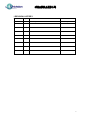
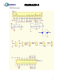
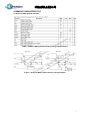
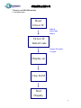
悠景科技股份有限公司
UG-5664ASYDF01
Evaluation Kit User Guide
Writer:
Email:
Version: Preliminary
1
悠景科技股份有限公司
Contents
1. REVISION HISTORY……………………………………………………………………………...3
2. EVK Schematic……………………………………………………………………………………..4
3. Symbol define………………………………………………………………………………………5
4. TIMMING CHARACTERISTICS…………………………...……………………………………...7
4.1 80-Series MPU parallel Interface ………………………………………………………..7
4.2 6800-Series MPU parallel Interface …………………………………………………….8
4.3 SPI(4-wire)-Series MPU parallel Interface……………………………………………..9
4.4 SPI(4-wire)-Series MPU parallel Interface……………………………………………10
5. EVK use introduction………………………………………………………………………..…..11
6.Power down and Power up Sequence……………………………………………………...…13
7. How to use SSD1322 module……………….………………………………………………….14
7.1 Initial Step Flow…………………………………………………………………………...14
7.2 RD recommend Initial Code for 80 Interface…………………………………………15
7.2.1 Sub Function for 80 Interface………………………………………………….15
2
悠景科技股份有限公司
1.REVISION HISTORY
Date
200X/XX/XX
Page
Contents
Version
Preliminary
Preliminary 0.0
3
悠景科技股份有限公司
2.EVK Schematic
4
悠景科技股份有限公司
3.Symbol define
D0-D7:These pins are bi-directional data bus connecting to the MCU data bus.
Unused pins are recommended to tie LOW. (Except for D2 pin in SPI mode)
E/RD#:This pin is MCU interface input.
When interfacing to a 6800-series microprocessor, this pin will be used as the Enable
(E) signal. Read/write operation is initiated when this pin is pulled HIGH and the chip
is selected.
When connecting to an 8080-microprocessor, this pin receives the Read (RD#) signal.
Read operation is initiated when this pin is pulled LOW and the chip is selected.
When serial interface is selected, this pin E(RD#) must be connected to VSS.
W/R# : This pin is read / write control input pin connecting to the MCU interface.
When interfacing to a 6800-series microprocessor, this pin will be used as Read/Write
(R/W#) selection input. Read mode will be carried out when this pin is pulled HIGH and
write mode when LOW.
When 8080 interface mode is selected, this pin will be the Write (WR#) input. Data
write operation is initiated when this pin is pulled LOW and the chip is selected.
When serial interface is selected, this pin R/W (WR#) must be connected to VSS.
D/C# : This pin is Data/Command control pin connecting to the MCU.
When the pin is pulled HIGH, the content at D[7:0] will be interpreted as data.
When the pin is pulled LOW, the content at D[7:0] will be interpreted as command.
RES# : This pin is reset signal input.
When the pin is pulled LOW, initialization of the chip is executed.
Keep this pin pull HIGH during normal operation.
CS# : This pin is the chip select input connecting to the MCU. The chip is enabled for MCU
communication only when CS# is pulled LOW.
BS0/BS1 : These pins are MCU interface selection input. See the following table:
5
悠景科技股份有限公司
VCC : This is the most positive voltage supply pin of the chip. It can be supplied externally or
generated internally by using internal DC-DC voltage converter.
VDD : This is a voltage supply pin. It must be connected to external source.
VDDIO : Power supply for interface logic level. It should be matched with the MCU interface
voltage level.
VCI : Low voltage power supply.
VCI must always be equal to or higher than VDD and VDDIO.
VSS : This is a ground pin. It also as a reference for the logic pins and the OLED driving
voltages. It must be connected to external ground.
NC : These pins should be left open individually.
6
悠景科技股份有限公司
4.TIMMING CHARACTERISTICS
4.1 80-Series MPU parallel Interface
Table 1 80-Series MPU parallel Interface Timing Characteristics
Figure 1 80-Series MPU parallel Interface Timing Diagram
7
悠景科技股份有限公司
4.2 6800-Series MPU parallel Interface
Table 1 80-Series MPU parallel Interface Timing Characteristics
Figure 1 80-Series MPU parallel Interface Timing Diagram
8
悠景科技股份有限公司
4.3 SPI(4-wire)-Series MPU parallel Interface
Table 1 SPI(4-wire)-Series MPU parallel Interface Timing Characteristics
Figure 1 SPI(4-wire)-Series MPU parallel Interface Timing Diagram
9
悠景科技股份有限公司
4.4 SPI(3-wire)-Series MPU parallel Interface
Table 1 SPI(3-wire)-Series MPU parallel Interface Timing Characteristics
Figure 1 SPI(4-wire)-Series MPU parallel Interface Timing Diagram
10
悠景科技股份有限公司
5.EVK use introduction
EVK
Module
Figure 5 EVK PCB and OLED Module
UG-5664ASYDF0101 is (COF) type module, please refer to Figure 5, Figure 6.User can use
leading wire to connect EVK with customer’s system. The example shows as Figure 7.
Figure 6 The combination of the module and EVK
11
悠景科技股份有限公司
Note 2
Note 4
Note 3
Note 1
Figure 7 EVK with test platform
Note 1:It is OLED high voltage supply.
Note 2:It is logic voltage supply.
Note 3:Those are leading wire connect to control board. Those are data pin.(D0-D7)
Note 4:Those are leading wire connect to control board. Those are control pin.
(E,R/W,D/C,RES,CS)
12
悠景科技股份有限公司
6.Power down and Power up Sequence
To protect OLED panel and extend the panel life time, the driver IC power
up/down routine should include a delay period between high voltage and low voltage
power sources during turn on/off. Such that panel has enough time to charge up or
discharge before/after operation.
Power up Sequence:
1.
2.
3.
4.
5.
6.
7.
Power up VDD
Send Display off command
Driver IC Initial Setting
Clear Screen
Power up VCC
Delay 100ms
(when VCC is stable)
VDD on
VCC on
Display on
VCC
VDD
VSS/Ground
Send Display on command
Power down Sequence:
1. Send Display off command
2. Power down VCC
3. Delay 100ms
(when VCC is reach 0 and
panel is completely
discharges)
4. Power down VDD
Display off
VCC off
VDD off
VCC
VDD
VSS/Ground
13
悠景科技股份有限公司
7.How to use SSD1322 module
7.1 Initial Step Flow
Reset
Driver IC
RES=0
Delay 10ms
RES=1
Driver IC
Initial Code
Suggest all register
set again
Display on
Clear RAM
Start
Dispaly
14
悠景科技股份有限公司
7.2 RD recommend Initial Code for 80 Interface:
15