1
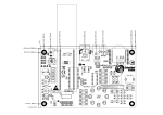
悠景科技股份有限公司
UG-2896GDEAF11
Application note
Evaluation Kit User Guide
Writer: Sean. Lai
Email: [email protected]
Version: Preliminary
1
悠景科技股份有限公司
Contents
1. REVISION HISTORY……………………………………………………………………………...3
2. EVK Schematic……………………………………………………………………………………..4
3. Symbol define………………………………………………………………………………………5
4. TIMMING CHARACTERISTICS…………………………...……………………………………...7
4.1 6800-Series MPU parallel Interface …………………………………...………………..7
4.2 8080-Series MPU parallel Interface …………………………………………………….8
4.3 4-bitSPI Interface ………………………...………………………………………………..9
4.4 3-bitSPI Interface ………...………………………………………………………………10
5. EVK use introduction………………………………………………………………………..…..11
6. Power down and Power up Sequence………………………………………………………..13
7. How to use SSD1351 module………………………………………………………………......14
7.1 Initial Step Flow…………………………………………………………………………...14
7.2 RD recommend Initial Code for 80 Interface…………………………………………15
7.2.1 Sub Function for 80 Interface………………………………………………….17
2
悠景科技股份有限公司
1. REVISION HISTORY
Date
Page
Contents
Version
2008/10/06
*
Preliminary
Preliminary 1.0
3
悠景科技股份有限公司
2. Schematic
2.1 EVK Schematic
4
悠景科技股份有限公司
3. Symbol define
D0-D7:These pins are bi-directional data bus connecting to the MCU data bus.
For SPI
application, D[0]=SCLK & D[1]=SDIN.
Unused pins are recommended to tie LOW except D[2].
BS0,BS1,BS2,BS3:MCU bus interface selection pins. Select appropriate logic setting as
described in the following table. BS3 and BS2 are command programmable (by command
ABh).[reset = 00]. BS1 and BS0 are pin select(J3, J4).
Regarding to the application of BS3 and BS2, they should be fixed as 00.
Table 1 – MCU Interface Selection Setting
E (RD#):This pin is MCU interface input.
When 6800 interface mode is selected, this pin will be used as the Enable (E) signal.
Read/write operation is initiated when this pin is pulled HIGH and the chip is selected.
When 8080 interface mode is selected, this pin receives the Read (RD#) signal. Read
operation is initiated when this pin is pulled LOW and the chip is selected.
When serial interface is selected, this pin E(RD#) must be connected to VSS.
R/W#:This pin is read / write control input pin connecting to the MCU interface.
When 6800 interface mode is selected, this pin will be used as Read/Write (R/W#)
selection input. Read mode will be carried out when this pin is pulled HIGH and
write mode when LOW.
When 8080 interface mode is selected, this pin will be the Write (WR#) input. Data
write operation is initiated when this pin is pulled LOW and the chip is selected.
When serial interface is selected, this pin R/W (WR#) must be connected to VSS.
D/C#:This pin is Data/Command control pin connecting to the MCU.
When the pin is pulled HIGH, the data at D[7:0] will be interpreted as data.
5
悠景科技股份有限公司
When the pin is pulled LOW, the data at D[7:0] will be interpreted as command.
4-Wire SPI Interface D/C pin Data/Command control pin connecting to the MCU.
3-Wire SPI Interface D/C pin Tie Low.
RES#:This pin is reset signal input.
When the pin is pulled LOW, initialization of the chip is executed.
Keep this pin pull HIGH during normal operation.
CS#:This pin is the chip select input connecting to the MCU.
The chip is enabled for MCU communication only when CS# is pulled LOW.
VCC:Power supply for panel driving voltage. This is also the most positive power voltage
supply pin. It is supplied by external high voltage source.
VCI:Low voltage power supply
GND:Power supply ground.
VDDIO:Power supply for interface logic level. It should match with the MCU interface
voltage level and must be connected to external source.
VSL:This is segment voltage reference pin.
When external VSL is not used, this pin should be left open.
When external VSL is used, connect with resistor and diode to ground. (details
depend on application)
VCOMH:COM signal deselected voltage level.
A capacitor should be connected between this pin and VSS.
GPIO0: Detail refer to Command B5h
GPIO1: Detail refer to Command B5h
6
悠景科技股份有限公司
4. TIMMING CHARACTERISTICS
4.1 6800-Series MPU parallel Interface
Figure 1 6800-series MCU parallel interface characteristics
Table 2 6800-Series MCU Parallel Interface Timing Characteristics
7
悠景科技股份有限公司
4.2 8080-Series MPU parallel Interface
Figure 2 8080-Series MCU Parallel Interface Timing Characteristics
Table 3 8080-Series MPU parallel Interface Timing Characteristics
8
悠景科技股份有限公司
4.3 4-Wire SPI Interface
Figure 3 Serial interface characteristics (4-wire SPI)
Table 4 Serial Interface Timing Characteristics (4-wire SPI)
9
悠景科技股份有限公司
4.4 3- Wire SPI Interface
Figure 4 Serial interface characteristics (3-wire SPI)
Table 5 Serial Interface Timing Characteristics (3-wire SPI)
10
悠景科技股份有限公司
5. EVK use introduction
Figure 5 EVK PCB and OLED Module
Push here to lock module
11
悠景科技股份有限公司
Figure 6 The combination of the module and EVK
Because the package of UG-2896GDEAF11 is COF, that the connect pads are on the top of
the module, and the connector which on the EVK PCB board is double size connect type. So
when assemble the module with EVK. The module must face up first and plug into the
connector. When finished assembled the module and EVK, then push the locking pad to lock
the module. See the figure 6.
When finished assembled the module and EVK. User can use leading wire to connect EVK
with customer’s system. The example shows as figure 7.
Note 1
Figure 7 control MCU connect with EVK
Note 1:It is the external most positive voltage supply. In this sample is connected to power
supply.
12
悠景科技股份有限公司
6. Power down and Power up Sequence
To protect OLED panel and extend the panel life time, the driver IC power
up/down routine should include a delay period between high voltage and low voltage
power sources during turn on/off. Such that panel has enough time to charge up or
discharge before/after operation.
Power up Sequence:
1. Power up VCI and VDDIO
2. Send Display off command
3. Driver IC Initial Setting
4. Clear Screen
5. Power up VCC
6. Delay 100ms
(when VCI is stable)
7. Send Display on command
VCI VDDIO on
VCC on
Display on
VCC
VCI
VSS/Ground
Power down Sequence:
1.
2.
3.
4.
Send Display off command
Power down VCC
Delay 100ms
Power down VCI and VDDIO
Display off
VCC off
VCI VDDIO off
V CC
V CI
VSS/Ground
13
悠景科技股份有限公司
7. How to use SSD1351 module
7.1 Initial Step Flow
Reset set
RES#=0
Delay 100ms
RES#=1
Initial IC
Clear RAM
Display on
Start send
data
14
悠景科技股份有限公司
7.2 RD recommend Initial Code for 8080 Interface
write_c(0xfd);
// Set Command Lock
write_d(0xb1);
write_c(0xae);
// Display off
write_c(0x15);
write_d(0x00);
write_d(0x7f);
//set column
write_c(0x75);
write_d(0x00);
write_d(0x5f);
//set row
write_c(0xa0);
write_d(0x74);
// Set Re-map / Color Depth
write_c(0xa1);
write_d(0x00);
// Set display start line
write_c(0xa2);
write_d(0x00);
// Set display offset
write_c(0xa6);
// Normal display
write_c(0xab);
write_d(0x00);
// Set Function selection
write_c(0xaf);
// Set Sleep mode
write_c(0xb1);
write_d(0x32);
// Set pre & dis_charge
write_c(0xb3);
write_d(0xf1);
// clock & frequency
write_c(0xb4);
write_d(0xa0);
write_d(0xb5);
write_d(0x55);
// Set Segment LOW Voltage
write_c(0xb5);
write_d(0x0A);
// Set GPIO
write_c(0xb6);
write_d(0x01);
// Set Second Pre-charge Period
write_c(0xb8);
write_d(0);
write_d(2);
write_d(3);
write_d(4);
write_d(5);
write_d(6);
write_d(7);
write_d(8);
write_d(9);
write_d(10);
write_d(11);
//Set Gray Table
//0
//1
//2
//3
//4
//5
//6
//7
//8
//9
//10
15
悠景科技股份有限公司
write_d(12);
write_d(13);
write_d(14);
write_d(15);
write_d(16);
write_d(17);
write_d(18);
write_d(19);
write_d(21);
write_d(23);
write_d(25);
write_d(27);
write_d(29);
write_d(31);
write_d(33);
write_d(35);
write_d(37);
write_d(39);
write_d(42);
write_d(45);
write_d(48);
write_d(51);
write_d(54);
write_d(57);
write_d(60);
write_d(63);
write_d(66);
write_d(69);
write_d(72);
write_d(76);
write_d(80);
write_d(84);
write_d(88);
write_d(92);
write_d(96);
write_d(100);
write_d(104);
write_d(108);
write_d(112);
write_d(116);
write_d(120);
write_d(125);
write_d(130);
write_d(135);
write_d(140);
write_d(145);
write_d(150);
write_d(155);
write_d(160);
write_d(165);
write_d(170);
write_d(175);
write_d(180);
//11
//12
//13
//14
//15
//16
//17
//18
//19
//20
//21
//22
//23
//24
//25
//26
//27
//28
//29
//30
//31
//32
//33
//34
//35
//36
//37
//38
//39
//40
//41
//42
//43
//44
//45
//46
//47
//48
//49
//50
//51
//52
//53
//54
//55
//56
//57
//58
//59
//60
//61
//62
//63
write_c(0xbb);
write_d(0x17);
// Set pre-charge voltage of color A B C
write_c(0xbe);
write_d(0x05);
// Set VcomH
16
悠景科技股份有限公司
write_c(0xc1);
write_d(0xc8);
write_d(0x80);
write_d(0x8a);
// Set contrast current for A B C
write_c(0xc7);
write_d(0x0f);
// Set master contrast
write_c(0xca);
write_d(0x5f);
// Duty
write_c(0xaf);
// Display on
7.2.1 Sub Function for 80 Interface
void write_c(unsigned char out_command)
{
DC=0;
CS=0;
RW=0;
P1=out_command;
RW=1;
CS=1;
DC=1;
}
void write_d(unsigned char out_data)
{
DC=1;
CS=0;
RW=0;
P1=out_data;
RW=1;
CS=1;
DC=0;
}
Note:1.For 80 series CPU interface.
2.For 8 Bbit Ttiple Transfer 65K support.
17