1
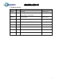
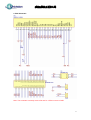
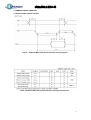
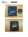
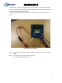
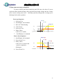
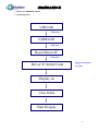
悠景科技股份有限公司
UG-6028GDEAF01
Evaluation Kit User Guide
Writer: Kathy. Huang
Email: [email protected]
Version: Preliminary
1
悠景科技股份有限公司
Contents
1. REVISION HISTORY……………………………………………………………………………...3
2. EVK Schematic……………………………………………………………………………………..4
3. Symbol define………………………………………………………………………………………5
4. TIMMING CHARACTERISTICS…………………………...……………………………………...6
4.1 80-Series MPU parallel Interface ………………………………………………………..6
4.2 6800-Series MPU parallel Interface …………………………………………………….7
4.3 SPI Interface ………………………………………………………………………………..8
5. EVK use introduction………………………………………………………………………..…...9
6. Power down and Power up Sequence………………………………………………………..11
7. How to use SEPS525F module………………………………………………………………...12
7.1 Initial Step Flow…………………………………………………………………………...12
7.2 RD recommend Initial Code for 80 Interface…………………………………………13
7.2.1 Sub Function for 80 Interface………………………………………………….15
2
悠景科技股份有限公司
1. REVISION HISTORY
Date
Page
Contents
Version
2006/3/9
*
Preliminary
Preliminary 0.0
2006/05/04
13
Initial setting
Preliminary 0.1
Modify 04h reg. : 0x01à0x03
2006/05/09
5
Add note itmes.
Preliminary0.2
2006/05/10
12
Power on sequence
Preliminary0.3
2005/05/25
11
Power down and Power up Sequence
Preliminary 0.4
3
悠景科技股份有限公司
2. EVK Schematic
Note: The schematic is already remove R3 and D1. VSDH connect to GND.
4
悠景科技股份有限公司
3. Symbol define
D17-D9:These pins are 9-bit bi-directional data bus to be connected to the MCU’s data bus.
The D10~D17 are for command and data inputs (8bit parallel interface).
CSB:These pins are CSB pins for master and slave driver IC. This pin is the chip
select input. The chip is enabled for MCU communication only when CSB is pulled low.
CPU : Selects the CPU type. Low:80-series CPU, High:68-Series CPU.
PS : Selects parallel/Serial interface type. Low: serial,High:parallel.
RDB:For an 80-system bus interface,read strobe signal(active low).For
For an 68-system bus interface,bus enable strobe(active high).
When using SPI,fix it to VDD or VSS level.
WRB:For an 80-system bus interface, write strobe signal (active low).
For an 68-system bus interface, read/write select.
Low: Write, High: Read. When using SPI, fix it to VDD or VSS level.
RESB:Reset SEPS525F(active low).
HV:External Column Driving Power Supply.
LV:Logic power supply.
GND:Power supply ground.
Note1: Please grounding for no use data pin.
Note2: If you are not used RGB Interface ,please grounding VSYNC,
HSYNC, Enable,DOTCLK and floating VSYNCO.
Note3: If you are not used VDDIO ,please connect to LV(VDD).
5
悠景科技股份有限公司
4. TIMMING CHARACTERISTICS
4.1 80-Series MPU parallel Interface
Figure 1 80-Series MPU 8-bit parallel Interface Timing Diagram
Table 1 80-Series MPU 8-bit parallel Interface Timing Characteristics
6
悠景科技股份有限公司
4.2 6800-Series MPU parallel Interface
Figure 2 68-Series MPU 8-bit parallel Interface Timing Diagram
Table 2 68-Series MPU 8-bit parallel Interface Timing Characteristics
7
悠景科技股份有限公司
4.3 SPI Interface
Figure 3 Serial peripheral interface Timing Diagram
Table 3 Serial peripheral interface Timing Characteristics
8
悠景科技股份有限公司
5. EVK use introduction
Interface select
Figure 4 EVK PCB and OLED Module
Push here to lock module
Figure5 The combination of the module and EVK
9
悠景科技股份有限公司
The SEPS525F is COF type package, that the connect pads are on the top of the module
connector. When finished assembled the module and EVK, then push the locking pad to lock
the module. See the Figure 4 and Figure5.
User can use leading wire to connect EVK with customer’s system. The example shows as
Figure 6
Note 2
Note 1
Fig 6 EVK with test platform
Note 1:It is the external most positive voltage supply. In this sample is connected to power
supply.
Note 2:The leading wire has 14 pins totally in this case.
(D17-D9, RDB,RS,WRB,RESB,CSB)
10
悠景科技股份有限公司
6. Power down and Power up Sequence
To protect OLED panel and extend the panel life time, the driver IC power
up/down routine should include a delay period between high voltage and low voltage
power sources during turn on/off. Such that panel has enough time to charge up or
discharge before/after operation.
Power up Sequence:
1.
2.
3.
4.
5.
6.
Power up VDD
Send Display off command
Driver IC Initial Setting
Clear Screen
Power up VDDH
Delay 100ms
(when VDD is stable)
7. Send Display on command
VDD on
VCC on
Display on
VCC
VDD
VSS/Ground
Power down Sequence:
1. Send Display off command
2. Power down VDDH
3. Delay 100ms
(when VDDH is reach 0 and
panel is completely
discharges)
4. Power down VDD
Display off
VCC off
VDD off
VCC
VDD
VSS/Ground
11
悠景科技股份有限公司
6. Power down and Power up Sequence
To protect OLED panel and extend the panel life time, the driver IC power
up/down routine should include a delay period between high voltage and low voltage
power sources during turn on/off. Such that panel has enough time to charge up or
discharge before/after operation.
Power up Sequence:
1.
2.
3.
4.
5.
6.
Power up VDD
Send Display off command
Driver IC Initial Setting
Clear Screen
Power up VDDH
Delay 100ms
(when VDD is stable)
7. Send Display on command
VDD on
VCC on
Display on
VCC
VDD
VSS/Ground
Power down Sequence:
1. Send Display off command
2. Power down VDDH
3. Delay 100ms
(when VDDH is reach 0 and
panel is completely
discharges)
4. Power down VDD
Display off
VCC off
VDD off
VCC
VDD
VSS/Ground
12
悠景科技股份有限公司
7. How to use SEPS525F module
7.1 Initial Step Flow
VDD ON
( Wait 1ms )
VDDH ON
( Wait 1ms )
Reset Driver IC
( Wait 1ms )
Driver IC Initial Code
Suggest all register
set again
Display on
Clear RAM
Start Dispaly
13
悠景科技股份有限公司
7.2 RD recommend Initial Code for 80 Interface
//Reg:04h Action:Normal current and PS ON ; Internal osc power off
Write_Command(rREDUCE_CURRENT,0x03);
T0_05sec();
//Reg:04h Action:Normal current and PS OFF
Write_Command(rREDUCE_CURRENT,0x00);
T0_05sec();
//Reg:3Bh Action:Screen Saver OFF
Write_Command(rSCREEN_SAVER_CONTEROL,0x00);
//Reg:02h Action:Export 0 /OSC with external resister/Internal OSC ON
Write_Command(rOSC_CTL,0x41);
//Reg:03h Action:FR=90Hz DIV=1
Write_Command(rCLOCK_DIV,0x30);
//Reg:80h Action:PDAC OFF,DDAC OFF/Reference Volt.control with external resister
Write_Command(rIREF,0x00);
//Reg:08h Action:set color R precharge time
Write_Command(rPRECHARGE_TIME_R,0x01);
//Reg:09h Action:set color G precharge time
Write_Command(rPRECHARGE_TIME_G,0x01);
//Reg:0Ah Action:set color B precharge tiem
Write_Command(rPRECHARGE_TIME_B,0x01);
//Reg:0Bh Action:set color R precharge current
Write_Command(rPRECHARGE_Current_R,0x0a);
//Reg:0Ch Action:set color G precharge current
Write_Command(rPRECHARGE_Current_G,0x0a);
//Reg:0Dh Action:set color B precharge current
Write_Command(rPRECHARGE_Current_B,0x0a);
//Reg:10h Action:set color R dot driving current
Write_Command(rDRIVING_CURRENT_R,0x52);
//Reg:11h Action:set color G dot driving current
Write_Command(rDRIVING_CURRENT_G,0x38);
//Reg:12h Action:set color B dot driving current
Write_Command(rDRIVING_CURRENT_B,0x3a);
//Reg:13h Action:Col D0 to D159/col normal display
Write_Command(rDISPLAY_MODE_SET,0x00);
//Reg:14h Action:MPU mode
Write_Command(rRGB_IF,0x31);
//Reg:16h Action:8btis dual transfer,65K support
Write_Command(rMEMORY_WRITE_MODE,0x66);
//Reg:17h Action:Memory addr.X start
Write_Command(rMX1_ADDR,0x00);
//Reg:18h Action:Memory addr.X end
Write_Command(rMX2_ADDR,0x9f);
//Reg:18h Action:Memory addr.Y start
Write_Command(rMY1_ADDR,0x00);
//Reg:1Ah Action:Memory addr.Y end
Write_Command(rMY2_ADDR,0x7f);
//Reg:20h Action:Memory X start addr.
Write_Command(rMEMORY_ACCESS_POINTER_X,0x00);
//Reg:21h Action:Memory Y start addr.
Write_Command(rMEMORY_ACCESS_POINTER_Y,0x00);
//Reg:28h Action:Display duty ratio
Write_Command(rDUTY,0x7f);
//Reg:29h Action:Display start line
Write_Command(rDSL,0x00);
//Reg:2Eh Action:Display First screen X start point
Write_Command(rD1_DDRAM_FAC,0x00);
14
悠景科技股份有限公司
//Reg:2Fh Action:Display First screen Y start point
Write_Command(rD1_DDRAM_FAR,0x00);
//Reg:31h Action:Display Second screen X start point
Write_Command(rD2_DDRAM_SAR,0x00);
//Reg:32h Action:Display Second screen Y start point
Write_Command(rD2_DDRAM_SAR,0x00);
//Reg:33h Action:Display size X start
Write_Command(rSCR1_FX1,0x00);
//Reg:34h Action:Display size X end
Write_Command(rSCR1_FX2,0x9f);
//Reg:35h Action:Display size Y start
Write_Command(rSCR1_FY1,0x00);
//Reg:36h Action:Display size Y end
Write_Command(rSCR1_FY2,0x7f);
//Reg:06h Action:Scan signal is high level at precharge period/Dispaly ON
Write_Command(rDISP_ON_OFF,0x01);
7.2.1 Sub Function for 80 Interface
void Write_Register(unsigned char data)
{
IOCLR = 0x0000000ff;//reset
D0~D7
IOCLR=bRS;
IOCLR=nCS;
IOCLR=nWR;
IOSET=data;
IOSET=nWR;
IOSET=nCS;
IOSET=bRS;
}
void Write_Parameter(unsigned char data)
{
IOCLR = 0x0000000ff;//reset
D0~D7
IOSET=bRS;
IOCLR=nCS;
IOCLR=nWR;
IOSET=data;
IOSET=nWR;
IOSET=nCS;
}
void Write_Command(unsigned char Reg, unsigned char data)
{
Write_Register(Reg);
Write_Parameter(data);
}
RD recommend Initial Code and Sub Function
Note:1.For 80 series CPU interface.
2.For 8bits DDRAM transfer.
15