1
RDC ®
R8822
RISC DSP Controller
Contents
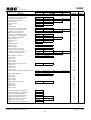
1. Features ......................................................................................................................... 5
2. Block Diagram .............................................................................................................. 6
3. Pin Configuration ......................................................................................................... 7
3.1
3.2
3.3
PQFP......................................................................................................................................7
LQFP......................................................................................................................................8
R8822 PQFP & LQFP Pin Out Table ....................................................................................9
4. Pin Description............................................................................................................ 10
4.1
R8822 I/O Characteristics of Each Pin................................................................................16
5. Basic Application System Block ................................................................................ 19
6. Read/Write Timing Diagram..................................................................................... 21
7. Crystal Characteristics............................................................................................... 23
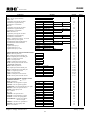
8. Execution Unit............................................................................................................. 24
8.1
8.2
8.3
8.4
General Registers.................................................................................................................24
Segment Registers ...............................................................................................................25
Instruction Pointer and Status Flags Registers ....................................................................25
Address Generation .............................................................................................................27
9. Peripheral Control Block Registers .......................................................................... 28
10.
Power Save & Power Down ................................................................................ 30
11.
Reset ...................................................................................................................... 33
12.
Bus Interface Unit................................................................................................ 35
12.1
Memory and I/O Interface ...................................................................................................35
RDC Semiconductor Co.
Subject to change without notice
Final Version 1.6
January 5, 2004
2