1
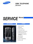
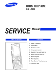
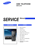
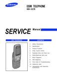
GSM TELEPHONE
SGH-D880
GSM TELEPHONE
CONTENTS
1.
Safety Precautions
2.
Specification
3.
Product Function
4.
Array course control
5.
Exploded View and Parts List
6.
Main Electrical Parts List
7.
Block Diagrams
8.
PCB Diagrams
9.
Flow Chart of Troubleshooting
10.
Reference data
11.
Disassembly and Assembly
Instructions
GSPN (Global Service Partner Network)
Country
North America
Latin America
CIS
Europe
China
Asia
Mideast & Africa
Web Site
service.samsungportal.com
latin.samsungportal.com
cis.samsungportal.com
europe.samsungportal.com
china.samsungportal.com
asia.samsungportal.com
mea.samsungportal.com
This Service Manual is a property of Samsung Electronics Co.,Ltd.
Any unauthorized use of Manual can be punished under applicable
International and/or domestic law.
ⓒ Samsung Electronics Co.,Ltd.
2007. 11 Rev.1.0
1. Safety Precautions
1-1. Repair Precaution
● Repair in Shield Box, during detailed tuning.
Take specially care of tuning or test, because specificity of cellular phone is sensitive for
surrounding interference(RF noise).
● Be careful to use a kind of magnetic object or tool, because performance of parts is
damaged by the influence of magnetic force.
● Surely use a standard screwdriver when you disassemble this product, otherwise screw will
be worn away.
● Use a thicken twisted wire when you measure level.
A thicken twisted wire has low resistance, therefore error of measurement is few.
● Repair after separate Test Pack and Set because for short danger (for example an
overcurrent and furious flames of parts etc) when you repair board in condition of
connecting Test Pack and tuning on.
● Take specially care of soldering, because Land of PCB is small and weak in heat.
● Surely tune on/off while using AC power plug, because a repair of battery charger is
dangerous when tuning ON/OFF PBA and Connector after disassembling charger.
● Don't use as you pleases after change other material than replacement registered on SEC
System.
Otherwise engineer in charge isn't charged with problem that you don't keep this rules.
1-1
SAMSUNG Proprietary-Contents may change without notice
This Document can not be used without Samsung's authorization
Safety Precautions
1-2. ESD(Electrostatically Sensitive Devices) Precaution
Several semiconductor may be damaged easily by static electricity. Such parts are called by
ESD(Electrostatically Sensitive Devices), for example IC,BGA chip etc. Read Precaution below.
You can prevent from ESD damage by static electricity.
● Remove static electricity remained your body before you touch semiconductor or parts with
semiconductor. There are ways that you touch an earthed place or wear static electricity
prevention string on wrist.
● Use earthed soldering steel when you connect or disconnect ESD.
● Use soldering removing tool to break static electricity. , otherwise ESD will be damaged by
static electricity.
● Don't unpack until you set up ESD on product. Because most of ESD are packed by box
and aluminum plate to have conductive power,they are prevented from static electricity.
● You must maintain electric contact between ESD and place due to be set up until ESD is
connected completely to the proper place or a circuit board.
1-2
SAMSUNG Proprietary-Contents may change without notice
This Document can not be used without Samsung's authorization
2. Specification
2-1. GSM General Specification
G SM900
Pha se 1
EG SM 900
Phase 2
DCS18 00
Ph ase 1
PCS190 0
Fr eq. Band [MHz]
Up link/ Do wnl ink
89 0~915
93 5~960
880~9 15
925~9 60
1 710~17 85
1 805~18 80
1 850~19 10
1 930~19 90
ARFCN ran ge
1 ~124
0~1 24 &
975~1 023
512~88 5
512~81 0
Tx/Rx spacin g
4 5MHz
45MHz
95MHz
80MHz
Mod. Bit rat e
/ Bit Per iod
270 .833kb ps
3. 692us
270.8 33kbps
3.69 2us
27 0.833 kbps
3.692 us
27 0.833 kbps
3.692 us
Time Slot Per iod
/ Fr am e Per iod
57 6.9us
4.6 15ms
576. 9us
4 .615ms
576.9 us
4. 615ms
576.9 us
4. 615ms
Mo dulat ion
0. 3G MSK
0.3G MSK
0.3G M SK
0.3G MSK
MS Power
33d Bm~5dBm
33dBm~ 5dBm
30 dBm~0d Bm
30 dBm~0d Bm
Po wer Class
5pcl ~ 19pcl
5pcl ~ 19pcl
0pcl ~ 15pcl
0pcl ~ 15pcl
Sen sitivity
-102 dBm
- 102dBm
-1 00dBm
-1 00dBm
TDM A M ux
8
8
8
8
Cell Radius
35Km
35Km
2Km
*PCS1900 only in Master
2-1
SAMSUNG Proprietary-Contents may change without notice
This Document can not be used without Samsung's authorization
Specification
2-2. GSM TX power class
TX Power
TX Power
TX Power
control level
GSM900
GSM850
control level
5
33±2 dBm
0
30±2 dBm
0
30±2 dBm
6
31±3 dBm
1
28±3 dBm
1
28±3 dBm
7
29±3 dBm
2
26±3 dBm
2
26±3 dBm
8
27±3 dBm
3
24±3 dBm
3
24±3 dBm
9
25±3 dBm
4
22±3 dBm
4
22±3 dBm
10
23±3 dBm
5
20±3 dBm
5
20±3 dBm
11
21±3 dBm
6
18±3 dBm
6
18±3 dBm
12
19±3 dBm
7
16±3 dBm
7
16±3 dBm
13
17±3 dBm
8
14±3 dBm
8
14±3 dBm
14
15±3 dBm
9
12±4 dBm
9
12±4 dBm
15
13±3 dBm
10
10±4 dBm
10
10±4 dBm
16
11±5 dBm
11
8±4dBm
11
8±4dBm
17
9±5 dBm
12
6±4 dBm
12
6±4 dBm
18
7±5 dBm
13
4±4 dBm
13
4±4 dBm
19
5±5 dBm
14
2±5 dBm
14
2±5 dBm
15
0±5 dBm
15
0±5 dBm
DCS1800
control level
PCS1900
*PCS1900 only in Master
2-2
SAMSUNG Proprietary-Contents may change without notice
This Document can not be used without Samsung's authorization
Specification
2-3. GSM EDGE TX power class
TX Power
Only in Master
TX Power
TX Power
control level
GSM900
GSM850
control level
8
27±3 dBm
2
26 -4/+3 dBm
2
26 -4/+3 dBm
9
25±3 dBm
3
24±3 dBm
3
24±3 dBm
10
23±3 dBm
4
22±3 dBm
4
22±3 dBm
11
21±3 dBm
5
20±3 dBm
5
20±3 dBm
12
19±3 dBm
6
18±3 dBm
6
18±3 dBm
13
17±3 dBm
7
16±3 dBm
7
16±3 dBm
14
15±3 dBm
8
12±3 dBm
8
12±3 dBm
15
13±3 dBm
9
10±3 dBm
9
10±3 dBm
16
11±5 dBm
10
14±3 dBm
10
14±3 dBm
17
9±5 dBm
11
12±4 dBm
11
12±4 dBm
18
7±5 dBm
12
10±4 dBm
12
10±4 dBm
19
5±5 dBm
13
8±4dBm
13
8±4dBm
14
6±4 dBm
14
6±4 dBm
15
4±4 dBm
15
4±4 dBm
DCS1800
control level
2-3
SAMSUNG Proprietary-Contents may change without notice
This Document can not be used without Samsung's authorization
PCS1900
Specification
2-4
SAMSUNG Proprietary-Contents may change without notice
This Document can not be used without Samsung's authorization
3. Operation Instruction and Installation
Main Function
-Slide Design Intenna
-Dual Standby
-3M AF CMOS Camera
-Bluetooth V.2.0
-Stereo Bluetooth Headset
-Mobile Tracker & SOS Messaging
-Large 2.3" QVGA 262K TFT Display
-EXT. Memory
-SMS/MMS/E-Mail
-WAP 2.0 / Java MIDP 2.0
-MP3, AAC, MP4, 3GPP Decoding
-Video Recording and Messaging
-GSM/GPRS/EDGE Class 10
-Band(Master : GSM900, 1800, 1900/ Slave : GSM900, 1800)
-TV-oput, FM radio
-Speaker Phone
3-1
SAMSUNG Proprietary-Contents may change without notice
This Document can not be used without Samsung's authorization
Operation Instruction and Installation
3-2
SAMSUNG Proprietary-Contents may change without notice
This Document can not be used without Samsung's authorization
4. Array course control
4-1. Software Adjustments
GH39-00877A
GH39-00876A
GH39-00875A
GH39-00872A
Test Jig (GH80-03306A)
Serial Cable(CSA LL64151-A)
Power Supply Cable
4-1
SAMSUNG Proprietary-Contents may change without notice
This Document can not be used without Samsung's authorization
Array course control
4-2. Software Downloading
4-2-1. Pre-requsite for Downloading
• Downloader Program(Gem_Downloader_1GNAND_ARM9+ARM7 v1.0.exe)
• D888 Mobile Phone
• Data Cable
• Binary file, TFS file
4-2-2. S/W Downloader Program
■ Load the binary download program by executing the
“Gem_Downloader_1GNAND_ARM9+ARM7 v1.0.exe”
1. Select the download mode you want.
-if Master mode wanted, check ARM9
-if Slave mode wanted, check ARM7
2. Select the connected serial port and the rate of speed
3. Select the check box, the mode you want to download.
- if the binary file wanted, check only 'BIN'
- if the tfs file wanted, check only 'TFS'
- if all the files wanted, check 'BIN+TFS'
4-2
SAMSUNG Proprietary-Contents may change without notice
This Document can not be used without Samsung's authorization
Array course control
3. Select the file(s) what you want to download
-if you select ARM9, select the file "D888ooooo_Master.ooo"
-if you select ARM7, select the file "D888ooooo_Slave.ooo"
4-3
SAMSUNG Proprietary-Contents may change without notice
This Document can not be used without Samsung's authorization
Array course control
4-4
SAMSUNG Proprietary-Contents may change without notice
This Document can not be used without Samsung's authorization
5. Exploded View and Parts List
5-1. Cellular phone Exploded View
QKP01
QMW01
QCK02
QFU01
QCK01
QCR58
QMP01
QME01
QMI01
QVK01
QKP02
QCA01
QSP01
QSH01
QAN03
QLC01
QME02
QAN02
QMO01
QVK09
QPC01
QRF03
QRE01
QFL01
QRF01
QSC05
QCR58
QFR01
QCR04
QHI01
QBA01
QFR02
QBA00
QVO01
5-1
SAMSUNG Proprietary-Contents may change without notice
This Document can not be used without Samsung's authorization
Exploded View and Parts List
5-2. Cellular phone Parts List
Design LOC
Description
SEC CODE
QAN02
INTENNA-SGHD888 MASTER
GH42-01277A
QAN03
INTENNA-SGHD888 SLAVE
GH42-01278A
QBA00
PMO COVER-BATT
GH72-43208A
QBA01
INNER BATTERY PACK-1200MAH,BLK
GH43-02570A
QCA01
CAMERA MODULE
GH59-04686A
QCK01
PMO KEY-CAMERA
GH72-42702A
QCK02
PMO KEY-SWITCH
GH72-42704B
QCR04
SCREW-MACHINE
6001-001479
QCR58
SCREW-MACHINE
6001-001870
QCR58
SCREW-MACHINE
6001-001870
QKP01
ASSY KEYPAD-MAIN(SER/BLK)
GH98-06250A
QKP02
ASSY KEYPAD-SUB(EU/BLK)
GH98-06251A
QLC01
ELA ETC-SGHD888 LCD MODULE
GH96-02740A
QME01
DOME SHEET-DOME SHEET 12KEY(MA
GH59-04694A
QME02
DOME SHEET-DOME SHEET 10KEY(SU
GH59-04695A
QMI01
MICROPHONE-ASSY-SGHD888
GH30-00400A
QMO01
MOTOR DC
GH31-00303A
QMP01
PBA MAIN-SGHD880
GH92-03970A
QPC01
MEA-SLIDER FPCB KIT(D880)
GH97-08361A
QRF01
TAPE-RF COVER
GH74-34624B
QSC05
RMO COVER-LOWER SCREW L
GH73-10853A
QSH01
ASSY COVER-SHIELD CAN
GH98-05452A
QSP01
ASSY ETC-MODULE SPEAKER
GH59-04744A
QVK01
KEY FPCB-VOLUME 2KEY
GH59-05174A
QVK09
FPC-SINGLE SIDE FPC(D888)
GH41-01987A
QVO01
PMO KEY-VOL
GH72-42703A
QRE01
ASSY CASE-REAR
GH98-05698A
PMO COVER-EAR IF
GH72-42701B
ASSY CASE-UPPER
GH98-06403A
ASSY COVER-MAIN WINODW(SER)
GH98-07047A
QRF03
QFU01
QMW01
5-2
SAMSUNG Proprietary-Contents may change without notice
This Document can not be used without Samsung's authorization
Exploded View and Parts List
Design LOC
Description
SEC CODE
ASSY CASE-FRONT SLIDE LOWER
GH98-06450B
QFL01
ASSY CASE-LOWER
GH98-05430B
QFR02
ASSY CASE-FRONT
GH98-05429B
QHI01
ASSY HINGE-MULTI TORSION SPRIN
GH98-05822A
QFR01
5-3
SAMSUNG Proprietary-Contents may change without notice
This Document can not be used without Samsung's authorization
Exploded View and Parts List
Description
SEC CODE
BAG PE
CBF INTERFACE-DLC APCBS10BBE(S
ADAPTOR-ATADS10EBE,BLK,EU
S/W CD-SGHD880 PC LINK CD
EARPHONE-AAEP405QBE,S20P,EU
LABEL(P)-UNIT SEAL
MANUAL-SFC
LABEL(R)-WATER SOAK
LABEL(R)-MAIN(SER)
MANUAL USERS-EU RUSSIAN
BOX-UNIT(SER)
CUSHION-CASE(EU)
TAPE INSU
TAPE INSU
TAPE GASK
TAPE GASK-SUB PCB1
TAPE INSU-SUB PCB
TAPE INSU
TAPE GASK
TAPE-REMOVE
TAPE GASK
VINYL-BOHO UPPER
TAPE INSU-PBA
TAPE-UPPER DOWN
TAPE GASK-LCD3
TAPE GASK-PBA MAIN2
TAPE-LCD
TAPE-FPCB
VINYL-BOHO SUB KEY
SPONGE
TAPE-SPK DECO
6902-000634
GH39-00922A
GH44-01702A
GH46-00535A
GH59-05296A
GH68-00518B
GH68-04336A
GH68-09361A
GH68-16409A
GH68-16604A
GH69-06063A
GH69-06065A
GH74-30410A
GH74-32729A
GH74-33529A
GH74-34627A
GH74-34629A
GH74-34677A
GH74-34813A
GH74-35112A
GH74-35775A
GH74-36200A
GH74-36228A
GH74-36285A
GH74-36536A
GH74-36537A
GH74-36538A
GH74-36539A
GH74-36626A
GH74-36646A
GH74-36658A
5-4
SAMSUNG Proprietary-Contents may change without notice
This Document can not be used without Samsung's authorization
6. MAIN Electrical Parts List
SEC Code
Design LOC
Description
STATUS
0403-001547
0403-001547
0406-001200
0406-001203
0406-001208
0406-001208
0406-001223
0406-001223
0406-001231
0406-001231
0406-001231
0406-001231
0406-001231
0406-001231
0406-001231
0406-001231
0406-001231
0406-001231
0406-001231
0406-001231
0406-001231
0406-001231
0406-001231
0505-002111
0505-002111
0601-002268
0601-002268
0801-003022
0801-003055
1001-001394
1001-001429
1001-001429
1001-001453
1001-001453
1001-001453
1001-001453
1001-001470
1001-001470
1001-001470
1003-002047
1009-001020
1106-001519
1108-000103
1108-000112
1201-002147
1201-002490
1201-002492
1201-002576
1203-004382
1203-004550
1203-004763
1203-004792
1203-004792
D400
D602
D300
D621
ZD600
ZD601
D500
D501
D603
D607
D608
D609
D611
D612
D613
D617
D618
D619
D620
D622
D623
D624
D625
Q800
U307
LED1
LED2
U305
U400
U601
U200
U201
U501
U502
U505
U507
U103
U500
U600
U402
U403
UME400
UME800
UME300
U303
PAM700
U506
PAM100
UPL400
UPL800
U603
U203
U401
DIODE-ZENER
DIODE-ZENER
DIODE-TVS
DIODE-TVS
DIODE-TVS
DIODE-TVS
DIODE-TVS
DIODE-TVS
DIODE-TVS
DIODE-TVS
DIODE-TVS
DIODE-TVS
DIODE-TVS
DIODE-TVS
DIODE-TVS
DIODE-TVS
DIODE-TVS
DIODE-TVS
DIODE-TVS
DIODE-TVS
DIODE-TVS
DIODE-TVS
DIODE-TVS
FET-SILICON
FET-SILICON
LED
LED
IC-CMOS LOGIC
IC-CMOS LOGIC
IC-ANALOG SWITCH
IC-ANALOG MULTIPLEX
IC-ANALOG MULTIPLEX
IC-ANALOG SWITCH
IC-ANALOG SWITCH
IC-ANALOG SWITCH
IC-ANALOG SWITCH
IC-ANALOG SWITCH
IC-ANALOG SWITCH
IC-ANALOG SWITCH
IC-MOTOR DRIVER
IC-HALL EFFECT S/W
IC-SRAM
IC-MCP
IC-MCP
IC-VIDEO AMP
IC-POWER AMP
IC-AUDIO AMP
IC-POWER AMP
IC-POWER SUPERVISOR
IC-POWER SUPERVISOR
IC-VOL. DETECTOR
IC-POSI.FIXED REG.
IC-POSI.FIXED REG.
SA
SA
SA
SA
SA
SA
SA
SA
SA
SA
SA
SA
SA
SA
SA
SA
SA
SA
SA
SA
SA
SA
SA
SA
SA
SA
SA
SA
SA
SA
SA
SA
SA
SA
SA
SA
SA
SA
SA
SA
SA
SA
SA
SA
SA
SA
SA
SA
SA
SA
SA
SA
SA
6-1
SAMSUNG Proprietary-Contents may change without notice
This Document can not be used without Samsung's authorization
Main Electrical Parts List
SEC Code
Design LOC
Description
STATUS
1203-004792
1203-004793
1203-004802
1203-004806
1203-004806
1203-004807
1205-003082
1205-003192
1205-003210
1205-003214
1205-003216
1205-003278
1205-003283
1404-001221
1404-001221
1405-001138
1405-001138
1405-001138
2007-000070
2007-000138
2007-000138
2007-000140
2007-000140
2007-000140
2007-000140
2007-000140
2007-000141
2007-000141
2007-000141
2007-000141
2007-000141
2007-000143
2007-000143
2007-000143
2007-000143
2007-000143
2007-000143
2007-000143
2007-000143
2007-000148
2007-000148
2007-000148
2007-000148
2007-000148
2007-000148
2007-000148
2007-000148
2007-000148
2007-000148
2007-000148
2007-000148
2007-000148
2007-000148
U503
U302
U300
U301
U306
U102
UCP200
UCP800
U304
U504
U101
U700
U104
TH800
U204
V200
V401
V800
R624
C830
C831
R107
R236
R330
R441
R841
R319
R320
R431
R832
R834
R110
R315
R703
R723
R724
R725
R726
R840
R100
R108
R204
R205
R214
R216
R228
R239
R246
R251
R256
R444
R506
R507
IC-POSI.FIXED REG.
IC-POSI.FIXED REG.
IC-POSI.FIXED REG.
IC-POSI.FIXED REG.
IC-POSI.FIXED REG.
IC-POSI.FIXED REG.
IC-COMM. CONTROLLER
IC-COMM. CONTROLLER
IC-CODEC
IC-CODEC
IC-TRANSCEIVER
IC-TRANSCEIVER
IC-TRANSCEIVER
THERMISTOR-NTC
THERMISTOR-NTC
VARISTOR
VARISTOR
VARISTOR
R-CHIP
R-CHIP
R-CHIP
R-CHIP
R-CHIP
R-CHIP
R-CHIP
R-CHIP
R-CHIP
R-CHIP
R-CHIP
R-CHIP
R-CHIP
R-CHIP
R-CHIP
R-CHIP
R-CHIP
R-CHIP
R-CHIP
R-CHIP
R-CHIP
R-CHIP
R-CHIP
R-CHIP
R-CHIP
R-CHIP
R-CHIP
R-CHIP
R-CHIP
R-CHIP
R-CHIP
R-CHIP
R-CHIP
R-CHIP
R-CHIP
SA
SA
SA
SA
SA
SA
SA
SA
SA
SA
SA
SA
SA
SA
SA
SA
SA
SA
SA
SA
SA
SA
SA
SA
SA
SA
SA
SA
SA
SA
SA
SA
SA
SA
SA
SA
SA
SA
SA
SA
SA
SA
SA
SA
SA
SA
SA
SA
SA
SA
SA
SA
SA
6-2
SAMSUNG Proprietary-Contents may change without notice
This Document can not be used without Samsung's authorization
Main Electrical Parts List
SEC Code
Design LOC
Description
STATUS
2007-000148
2007-000149
2007-000157
2007-000157
2007-000157
2007-000157
2007-000157
2007-000157
2007-000157
2007-000159
2007-000162
2007-000162
2007-000162
2007-000162
2007-000162
2007-000162
2007-000162
2007-000162
2007-000162
2007-000162
2007-000162
2007-000162
2007-000162
2007-000162
2007-000162
2007-000162
2007-000162
2007-000162
2007-000162
2007-000162
2007-000162
2007-000162
2007-000162
2007-000162
2007-000162
2007-000162
2007-000162
2007-000162
2007-000162
2007-000162
2007-000162
2007-000166
2007-000170
2007-000171
2007-000171
2007-000171
2007-000171
2007-000171
2007-000171
2007-000171
2007-000171
2007-000171
2007-000171
R860
R439
R223
R225
R226
R515
R846
R847
R851
R333
R206
R247
R309
R310
R312
R316
R322
R323
R331
R332
R334
R408
R410
R411
R412
R414
R416
R420
R426
R433
R620
R621
R813
R826
R827
R828
R842
R843
R844
R855
R858
R335
R314
C725
L700
R253
R422
R425
R446
R447
R449
R450
R451
R-CHIP
R-CHIP
R-CHIP
R-CHIP
R-CHIP
R-CHIP
R-CHIP
R-CHIP
R-CHIP
R-CHIP
R-CHIP
R-CHIP
R-CHIP
R-CHIP
R-CHIP
R-CHIP
R-CHIP
R-CHIP
R-CHIP
R-CHIP
R-CHIP
R-CHIP
R-CHIP
R-CHIP
R-CHIP
R-CHIP
R-CHIP
R-CHIP
R-CHIP
R-CHIP
R-CHIP
R-CHIP
R-CHIP
R-CHIP
R-CHIP
R-CHIP
R-CHIP
R-CHIP
R-CHIP
R-CHIP
R-CHIP
R-CHIP
R-CHIP
R-CHIP
R-CHIP
R-CHIP
R-CHIP
R-CHIP
R-CHIP
R-CHIP
R-CHIP
R-CHIP
R-CHIP
SA
SA
SA
SA
SA
SA
SA
SA
SA
SA
SA
SA
SA
SA
SA
SA
SA
SA
SA
SA
SA
SA
SA
SA
SA
SA
SA
SA
SA
SA
SA
SA
SA
SA
SA
SA
SA
SA
SA
SA
SA
SA
SA
SA
SA
SA
SA
SA
SA
SA
SA
SA
SA
6-3
SAMSUNG Proprietary-Contents may change without notice
This Document can not be used without Samsung's authorization
Main Electrical Parts List
SEC Code
Design LOC
Description
STATUS
2007-000171
2007-000171
2007-000171
2007-000171
2007-000171
2007-000171
2007-000171
2007-000171
2007-000171
2007-000171
2007-000171
2007-000171
2007-000171
2007-000171
2007-000174
2007-000242
2007-000242
2007-000636
2007-000758
2007-000758
2007-000758
2007-000758
2007-000831
2007-000932
2007-000932
2007-000932
2007-000932
2007-001291
2007-001291
2007-001292
2007-001292
2007-001306
2007-001319
2007-001319
2007-001319
2007-001319
2007-001333
2007-001333
2007-001333
2007-001333
2007-001339
2007-003001
2007-003001
2007-007009
2007-007092
2007-007100
2007-007107
2007-007107
2007-007107
2007-007107
2007-007137
2007-007137
2007-007137
R513
R520
R521
R523
R618
R619
R622
R623
R718
R719
R848
R853
R859
U703
R805
C636
R857
R856
R218
R235
R438
R838
R440
R716
R717
R721
R722
R610
R613
R442
R443
R318
R240
R241
R248
R249
R328
R448
R603
R606
R835
R714
R720
R317
R701
R815
R237
R250
R821
R830
R503
R504
R508
R-CHIP
R-CHIP
R-CHIP
R-CHIP
R-CHIP
R-CHIP
R-CHIP
R-CHIP
R-CHIP
R-CHIP
R-CHIP
R-CHIP
R-CHIP
R-CHIP
R-CHIP
R-CHIP
R-CHIP
R-CHIP
R-CHIP
R-CHIP
R-CHIP
R-CHIP
R-CHIP
R-CHIP
R-CHIP
R-CHIP
R-CHIP
R-CHIP
R-CHIP
R-CHIP
R-CHIP
R-CHIP
R-CHIP
R-CHIP
R-CHIP
R-CHIP
R-CHIP
R-CHIP
R-CHIP
R-CHIP
R-CHIP
R-CHIP
R-CHIP
R-CHIP
R-CHIP
R-CHIP
R-CHIP
R-CHIP
R-CHIP
R-CHIP
R-CHIP
R-CHIP
R-CHIP
SA
SA
SA
SA
SA
SA
SA
SA
SA
SA
SA
SA
SA
SA
SA
SA
SA
SA
SA
SA
SA
SA
SA
SA
SA
SA
SA
SA
SA
SA
SA
SA
SA
SA
SA
SA
SA
SA
SA
SA
SA
SA
SA
SA
SA
SA
SA
SA
SA
SA
SA
SA
SA
6-4
SAMSUNG Proprietary-Contents may change without notice
This Document can not be used without Samsung's authorization
Main Electrical Parts List
SEC Code
Design LOC
Description
STATUS
2007-007137
2007-007137
2007-007139
2007-007142
2007-007142
2007-007311
2007-007312
2007-007317
2007-007318
2007-007318
2007-007318
2007-007334
2007-007334
2007-007489
2007-007573
2007-007573
2007-007981
2007-008055
2007-008354
2007-008516
2007-009084
2007-009084
2203-000233
2203-000233
2203-000233
2203-000254
2203-000254
2203-000254
2203-000254
2203-000254
2203-000254
2203-000278
2203-000278
2203-000278
2203-000278
2203-000278
2203-000278
2203-000278
2203-000278
2203-000278
2203-000311
2203-000311
2203-000330
2203-000330
2203-000425
2203-000425
2203-000425
2203-000425
2203-000425
2203-000425
2203-000425
2203-000425
2203-000425
R509
R516
R852
R607
R615
R429
R614
R519
R435
R510
R511
R616
R850
R102
R400
R849
R604
R61
R402
R229
R244
R245
C113
C128
C411
C202
C610
C717
C802
C805
C808
C112
C124
C126
C127
C154
C511
C512
C711
C721
C131
C606
C152
C153
C222
C224
C320
C321
C329
C413
C414
C600
C609
R-CHIP
R-CHIP
R-CHIP
R-CHIP
R-CHIP
R-CHIP
R-CHIP
R-CHIP
R-CHIP
R-CHIP
R-CHIP
R-CHIP
R-CHIP
R-CHIP
R-CHIP
R-CHIP
R-CHIP
R-CHIP
R-CHIP
R-CHIP
R-CHIP
R-CHIP
C-CER,CHIP
C-CER,CHIP
C-CER,CHIP
C-CER,CHIP
C-CER,CHIP
C-CER,CHIP
C-CER,CHIP
C-CER,CHIP
C-CER,CHIP
C-CER,CHIP
C-CER,CHIP
C-CER,CHIP
C-CER,CHIP
C-CER,CHIP
C-CER,CHIP
C-CER,CHIP
C-CER,CHIP
C-CER,CHIP
C-CER,CHIP
C-CER,CHIP
C-CER,CHIP
C-CER,CHIP
C-CER,CHIP
C-CER,CHIP
C-CER,CHIP
C-CER,CHIP
C-CER,CHIP
C-CER,CHIP
C-CER,CHIP
C-CER,CHIP
C-CER,CHIP
SA
SA
SA
SA
SA
SA
SA
SA
SA
SA
SA
SA
SA
SA
SA
SA
SA
SA
SA
SA
SA
SA
SA
SA
SA
SA
SA
SA
SA
SA
SA
SA
SA
SA
SA
SA
SA
SA
SA
SA
SA
SA
SA
SA
SA
SA
SA
SA
SA
SA
SA
SA
SA
6-5
SAMSUNG Proprietary-Contents may change without notice
This Document can not be used without Samsung's authorization
Main Electrical Parts List
SEC Code
Design LOC
Description
STATUS
2203-000425
2203-000425
2203-000438
2203-000438
2203-000466
2203-000466
2203-000489
2203-000679
2203-000714
2203-000812
2203-000812
2203-000812
2203-000812
2203-000812
2203-000812
2203-000812
2203-000812
2203-000812
2203-000812
2203-000812
2203-000812
2203-000812
2203-000812
2203-000812
2203-000812
2203-000812
2203-000812
2203-000812
2203-000854
2203-000995
2203-000995
2203-000995
2203-000995
2203-000995
2203-000995
2203-000995
2203-000995
2203-001072
2203-001201
2203-001239
2203-001239
2203-001239
2203-001239
2203-001239
2203-001259
2203-001385
2203-001385
2203-001437
2203-001437
2203-002443
2203-002677
2203-002677
2203-002709
C814
C816
C100
C148
C716
C718
C709
C812
C433
C120
C121
C129
C137
C138
C139
C140
C141
C229
C302
C303
C628
C704
C706
C707
C708
C821
C841
R713
C811
C103
C108
C507
C553
C554
C603
C722
C723
R707
C700
C544
C545
C637
C638
C639
C602
C713
C714
C601
C608
C435
C116
C146
C109
C-CER,CHIP
C-CER,CHIP
C-CER,CHIP
C-CER,CHIP
C-CER,CHIP
C-CER,CHIP
C-CER,CHIP
C-CER,CHIP
C-CER,CHIP
C-CER,CHIP
C-CER,CHIP
C-CER,CHIP
C-CER,CHIP
C-CER,CHIP
C-CER,CHIP
C-CER,CHIP
C-CER,CHIP
C-CER,CHIP
C-CER,CHIP
C-CER,CHIP
C-CER,CHIP
C-CER,CHIP
C-CER,CHIP
C-CER,CHIP
C-CER,CHIP
C-CER,CHIP
C-CER,CHIP
C-CER,CHIP
C-CER,CHIP
C-CER,CHIP
C-CER,CHIP
C-CER,CHIP
C-CER,CHIP
C-CER,CHIP
C-CER,CHIP
C-CER,CHIP
C-CER,CHIP
C-CER,CHIP
C-CER,CHIP
C-CER,CHIP
C-CER,CHIP
C-CER,CHIP
C-CER,CHIP
C-CER,CHIP
C-CER,CHIP
C-CER,CHIP
C-CER,CHIP
C-CER,CHIP
C-CER,CHIP
C-CER,CHIP
C-CER,CHIP
C-CER,CHIP
C-CER,CHIP
SA
SA
SA
SA
SA
SA
SA
SA
SA
SA
SA
SA
SA
SA
SA
SA
SA
SA
SA
SA
SA
SA
SA
SA
SA
SA
SA
SA
SA
SA
SA
SA
SA
SA
SA
SA
SA
SA
SA
SA
SA
SA
SA
SA
SA
SA
SA
SA
SA
SA
SA
SA
SA
6-6
SAMSUNG Proprietary-Contents may change without notice
This Document can not be used without Samsung's authorization
Main Electrical Parts List
SEC Code
Design LOC
Description
STATUS
2203-005050
2203-005050
2203-005050
2203-005052
2203-005234
2203-005288
2203-005288
2203-005288
2203-005288
2203-005288
2203-005395
2203-005482
2203-005482
2203-005482
2203-005482
2203-005482
2203-005482
2203-005482
2203-005482
2203-005482
2203-005482
2203-005482
2203-005482
2203-005482
2203-005482
2203-005482
2203-005482
2203-005482
2203-005482
2203-005482
2203-005482
2203-005482
2203-005482
2203-005482
2203-005482
2203-005482
2203-005482
2203-005482
2203-005482
2203-005482
2203-005482
2203-005482
2203-005482
2203-005483
2203-005496
2203-005496
2203-005496
2203-005496
2203-005496
2203-005496
2203-005496
2203-005496
2203-005496
C110
C114
C508
C701
C702
C101
C104
C117
C119
L101
C134
C214
C307
C309
C310
C311
C313
C314
C315
C319
C505
C506
C509
C510
C516
C519
C520
C521
C530
C531
C537
C540
C542
C543
C555
C710
C712
C720
C724
C809
C810
C813
C838
C826
C118
C149
C200
C201
C203
C204
C205
C207
C208
C-CER,CHIP
C-CER,CHIP
C-CER,CHIP
C-CER,CHIP
C-CER,CHIP
C-CER,CHIP
C-CER,CHIP
C-CER,CHIP
C-CER,CHIP
C-CER,CHIP
C-CER,CHIP
C-CER,CHIP
C-CER,CHIP
C-CER,CHIP
C-CER,CHIP
C-CER,CHIP
C-CER,CHIP
C-CER,CHIP
C-CER,CHIP
C-CER,CHIP
C-CER,CHIP
C-CER,CHIP
C-CER,CHIP
C-CER,CHIP
C-CER,CHIP
C-CER,CHIP
C-CER,CHIP
C-CER,CHIP
C-CER,CHIP
C-CER,CHIP
C-CER,CHIP
C-CER,CHIP
C-CER,CHIP
C-CER,CHIP
C-CER,CHIP
C-CER,CHIP
C-CER,CHIP
C-CER,CHIP
C-CER,CHIP
C-CER,CHIP
C-CER,CHIP
C-CER,CHIP
C-CER,CHIP
C-CER,CHIP
C-CER,CHIP
C-CER,CHIP
C-CER,CHIP
C-CER,CHIP
C-CER,CHIP
C-CER,CHIP
C-CER,CHIP
C-CER,CHIP
C-CER,CHIP
SA
SA
SA
SA
SA
SA
SA
SA
SA
SA
SA
SA
SA
SA
SA
SA
SA
SA
SA
SA
SA
SA
SA
SA
SA
SA
SA
SA
SA
SA
SA
SA
SA
SA
SA
SA
SA
SA
SA
SA
SA
SA
SA
SA
SA
SA
SA
SA
SA
SA
SA
SA
SA
6-7
SAMSUNG Proprietary-Contents may change without notice
This Document can not be used without Samsung's authorization
Main Electrical Parts List
SEC Code
Design LOC
Description
STATUS
2203-005496
2203-005496
2203-005496
2203-005496
2203-005682
2203-005682
2203-005719
2203-005719
2203-005993
2203-005993
2203-006048
2203-006048
2203-006048
2203-006048
2203-006048
2203-006048
2203-006048
2203-006048
2203-006048
2203-006048
2203-006048
2203-006048
2203-006048
2203-006048
2203-006048
2203-006048
2203-006048
2203-006048
2203-006048
2203-006048
2203-006048
2203-006048
2203-006048
2203-006048
2203-006257
2203-006257
2203-006257
2203-006257
2203-006257
2203-006257
2203-006257
2203-006257
2203-006257
2203-006257
2203-006257
2203-006257
2203-006260
2203-006260
2203-006260
2203-006260
2203-006260
2203-006260
2203-006324
C209
C210
C211
C213
C206
C212
C216
C823
C533
C534
C130
C132
C133
C144
C300
C416
C417
C423
C427
C546
C547
C604
C607
C631
C632
C633
C800
C801
C803
C804
C806
C807
C834
C835
C401
C402
C404
C406
C408
C412
C421
C815
C829
C832
C836
C837
C532
C535
C549
C550
C551
C552
C422
C-CER,CHIP
C-CER,CHIP
C-CER,CHIP
C-CER,CHIP
C-CER,CHIP
C-CER,CHIP
C-CER,CHIP
C-CER,CHIP
C-CER,CHIP
C-CER,CHIP
C-CER,CHIP
C-CER,CHIP
C-CER,CHIP
C-CER,CHIP
C-CER,CHIP
C-CER,CHIP
C-CER,CHIP
C-CER,CHIP
C-CER,CHIP
C-CER,CHIP
C-CER,CHIP
C-CER,CHIP
C-CER,CHIP
C-CER,CHIP
C-CER,CHIP
C-CER,CHIP
C-CER,CHIP
C-CER,CHIP
C-CER,CHIP
C-CER,CHIP
C-CER,CHIP
C-CER,CHIP
C-CER,CHIP
C-CER,CHIP
C-CER,CHIP
C-CER,CHIP
C-CER,CHIP
C-CER,CHIP
C-CER,CHIP
C-CER,CHIP
C-CER,CHIP
C-CER,CHIP
C-CER,CHIP
C-CER,CHIP
C-CER,CHIP
C-CER,CHIP
C-CER,CHIP
C-CER,CHIP
C-CER,CHIP
C-CER,CHIP
C-CER,CHIP
C-CER,CHIP
C-CER,CHIP
SA
SA
SA
SA
SA
SA
SA
SA
SA
SA
SA
SA
SA
SA
SA
SA
SA
SA
SA
SA
SA
SA
SA
SA
SA
SA
SA
SA
SA
SA
SA
SA
SA
SA
SA
SA
SA
SA
SA
SA
SA
SA
SA
SA
SA
SA
SA
SA
SA
SA
SA
SA
SA
6-8
SAMSUNG Proprietary-Contents may change without notice
This Document can not be used without Samsung's authorization
Main Electrical Parts List
SEC Code
Design LOC
Description
STATUS
2203-006348
2203-006361
2203-006399
2203-006399
2203-006399
2203-006399
2203-006399
2203-006399
2203-006399
2203-006399
2203-006399
2203-006399
2203-006399
2203-006399
2203-006399
2203-006399
2203-006399
2203-006399
2203-006474
2203-006562
2203-006562
2203-006562
2203-006562
2203-006562
2203-006562
2203-006562
2203-006562
2203-006562
2203-006562
2203-006562
2203-006562
2203-006562
2203-006824
2203-006824
2203-006824
2203-006824
2203-006824
2203-006824
2203-006825
2203-006838
2203-006838
2203-006838
2203-006838
2203-006838
2203-006838
2203-006838
2203-006838
2203-006838
2203-006838
2203-006838
2203-006838
2203-006839
2203-006839
C415
C425
C125
C223
C226
C306
C312
C326
C328
C429
C431
C434
C523
C524
C526
C615
C630
C827
C426
C106
C142
C225
C227
C228
C316
C325
C327
C420
C430
C525
C528
C629
C403
C407
C410
C424
C825
C828
C405
C102
C107
C122
C123
C301
C304
C305
C308
C317
C324
C418
C419
C219
C824
C-CER,CHIP
C-CER,CHIP
C-CER,CHIP
C-CER,CHIP
C-CER,CHIP
C-CER,CHIP
C-CER,CHIP
C-CER,CHIP
C-CER,CHIP
C-CER,CHIP
C-CER,CHIP
C-CER,CHIP
C-CER,CHIP
C-CER,CHIP
C-CER,CHIP
C-CER,CHIP
C-CER,CHIP
C-CER,CHIP
C-CER,CHIP
C-CER,CHIP
C-CER,CHIP
C-CER,CHIP
C-CER,CHIP
C-CER,CHIP
C-CER,CHIP
C-CER,CHIP
C-CER,CHIP
C-CER,CHIP
C-CER,CHIP
C-CER,CHIP
C-CER,CHIP
C-CER,CHIP
C-CER,CHIP
C-CER,CHIP
C-CER,CHIP
C-CER,CHIP
C-CER,CHIP
C-CER,CHIP
C-CER,CHIP
C-CER,CHIP
C-CER,CHIP
C-CER,CHIP
C-CER,CHIP
C-CER,CHIP
C-CER,CHIP
C-CER,CHIP
C-CER,CHIP
C-CER,CHIP
C-CER,CHIP
C-CER,CHIP
C-CER,CHIP
C-CER,CHIP
C-CER,CHIP
SA
SA
SA
SA
SA
SA
SA
SA
SA
SA
SA
SA
SA
SA
SA
SA
SA
SA
SA
SA
SA
SA
SA
SA
SA
SA
SA
SA
SA
SA
SA
SA
SA
SA
SA
SA
SA
SA
SA
SA
SA
SA
SA
SA
SA
SA
SA
SA
SA
SA
SA
SA
SA
6-9
SAMSUNG Proprietary-Contents may change without notice
This Document can not be used without Samsung's authorization
Main Electrical Parts List
SEC Code
Design LOC
Description
STATUS
2203-006841
2203-006841
2404-001225
2404-001225
2404-001225
2404-001225
2404-001226
2404-001381
2404-001381
2404-001396
2404-001396
2404-001414
2404-001414
2404-001430
2404-001506
2404-001506
2404-001506
2703-001259
2703-001737
2703-001737
2703-001752
2703-002170
2703-002205
2703-002313
2703-002314
2703-002367
2703-002368
2703-002544
2703-002558
2703-002558
2703-002586
2703-002608
2703-002608
2703-002701
2703-003290
2801-004455
2801-004466
2801-004466
2801-004587
2801-004587
2801-004682
2901-001286
2901-001286
2901-001286
2901-001286
2901-001286
2901-001315
2901-001408
2901-001463
2901-001463
2904-001744
2909-001279
2911-000087
C436
C844
TA300
TA505
TA507
TA508
TA506
TA400
TA800
TA502
TA503
TA500
TA501
TA504
TA100
TA600
TA700
L600
L702
L703
L701
C136
L100
L102
L105
L113
C705
L709
L110
L707
L112
L106
L108
L104
L400
OSC700
OSC400
OSC800
OSC100
OSC101
OSC300
F602
F603
F604
F605
F606
F200
F607
F400
F401
F700
F100
F101
C-CER,CHIP
C-CER,CHIP
C-TA,CHIP
C-TA,CHIP
C-TA,CHIP
C-TA,CHIP
C-TA,CHIP
C-TA,CHIP
C-TA,CHIP
C-TA,CHIP
C-TA,CHIP
C-TA,CHIP
C-TA,CHIP
C-TA,CHIP
C-TA,CHIP
C-TA,CHIP
C-TA,CHIP
INDUCTOR-SMD
INDUCTOR-SMD
INDUCTOR-SMD
INDUCTOR-SMD
INDUCTOR-SMD
INDUCTOR-SMD
INDUCTOR-SMD
INDUCTOR-SMD
INDUCTOR-SMD
INDUCTOR-SMD
INDUCTOR-SMD
INDUCTOR-SMD
INDUCTOR-SMD
INDUCTOR-SMD
INDUCTOR-SMD
INDUCTOR-SMD
INDUCTOR-SMD
INDUCTOR-SMD
CRYSTAL-SMD
CRYSTAL-SMD
CRYSTAL-SMD
CRYSTAL-SMD
CRYSTAL-SMD
CRYSTAL-SMD
FILTER-EMI SMD
FILTER-EMI SMD
FILTER-EMI SMD
FILTER-EMI SMD
FILTER-EMI SMD
FILTER-EMI SMD
FILTER-EMI SMD
FILTER-EMI SMD
FILTER-EMI SMD
FILTER-SAW
FILTER-LC
DUPLEXER-FEM
SA
SA
SA
SA
SA
SA
SA
SA
SA
SA
SA
SA
SA
SA
SA
SA
SA
SA
SA
SA
SA
SA
SA
SA
SA
SA
SA
SA
SA
SA
SA
SA
SA
SA
SA
SA
SA
SA
SA
SA
SA
SA
SA
SA
SA
SA
SA
SA
SA
SA
SA
SA
SA
6-10
SAMSUNG Proprietary-Contents may change without notice
This Document can not be used without Samsung's authorization
Main Electrical Parts List
SEC Code
Design LOC
Description
STATUS
3301-001120
3301-001438
3301-001438
3301-001438
3301-001438
3301-001438
3301-001438
3301-001438
3301-001438
3301-001534
3301-001534
3301-001534
3301-001534
3301-001534
3301-001534
3301-001534
3301-001534
3301-001534
3301-001534
3301-001659
3301-001812
3301-001876
3301-001876
3301-001885
3301-001885
3301-001885
3404-001152
3404-001152
3705-001358
3705-001421
3709-001394
3709-001447
3709-001447
3710-002499
3711-006228
3711-006568
4202-001391
4302-001181
L401
L500
L501
L502
L503
L507
L509
L513
L514
L200
L300
L301
L504
L505
L506
L508
L510
L511
L519
L111
L403
L517
L518
L601
L602
L603
TAC3
TAC4
RFS100
RFS700
CD300
SIM200
SIM800
IFC601
BTC600
HEA616
ANT102
BAT400
BEAD-SMD
BEAD-SMD
BEAD-SMD
BEAD-SMD
BEAD-SMD
BEAD-SMD
BEAD-SMD
BEAD-SMD
BEAD-SMD
BEAD-SMD
BEAD-SMD
BEAD-SMD
BEAD-SMD
BEAD-SMD
BEAD-SMD
BEAD-SMD
BEAD-SMD
BEAD-SMD
BEAD-SMD
BEAD-SMD
BEAD-SMD
BEAD-SMD
BEAD-SMD
BEAD-SMD
BEAD-SMD
BEAD-SMD
SWITCH-TACT
SWITCH-TACT
CONNECTOR-COAXIAL
CONNECTOR-COAXIAL
CONNECTOR-CARD EDGE
CONNECTOR-CARD EDGE
CONNECTOR-CARD EDGE
SOCKET-INTERFACE
HEADER-BATTERY
HEADER-BOARD TO BOARD
ANTENNA-CHIP
BATTERY-LI(2ND)
SA
SA
SA
SA
SA
SA
SA
SA
SA
SA
SA
SA
SA
SA
SA
SA
SA
SA
SA
SA
SA
SA
SA
SA
SA
SA
SA
SA
SA
SA
SA
SA
SA
SA
SA
SA
SA
SA
Please consult the GSPN website (Samsung Portal) for the most recent version of the product's
part list.
6-11
SAMSUNG Proprietary-Contents may change without notice
This Document can not be used without Samsung's authorization
Main Electrical Parts List
6-12
SAMSUNG Proprietary-Contents may change without notice
This Document can not be used without Samsung's authorization
7. Block Diagrams
7-1. Functional Block Diagram
7-1
Block Diagrams
7-2. BLUETOOTH/FM Radio Block Diagram
7-2
8. PCB Diagrams
- Main top view
8-1
PCB Diagrams
- Main bottom view
8-2
9. Flow Chart of Troubleshooting
9-1. Power On
' Power On ' does not work
Yes
No
Check the Battery Voltage
Change the Battery
is more than 3.4V
Yes
No
C421(VISA) = 2.7V?
Check the PMU related to VINT
Yes
No
Check the Clock at
Resolder OSC400
R404=32KHZ
Yes
No
C401(+VDD_IO_LOW_1.8V) &
C402(+VDD_IO_HIGH_2.8V) =
"H"?
Check the related circuit
Yes
No
C426(+VDD_GSM_CORE_1.2V)
= 1.2V?
Check the +VDD_GSM_CORE_1.2V
circuit
Yes
Check the initial operation
Yes
END
9-1
SAMSUNG Proprietary-Contents may change without notice
This Document can not be used without Samsung's authorization
Flow Chart of Troubleshooting
9-2
SAMSUNG Proprietary-Contents may change without notice
This Document can not be used without Samsung's authorization
Flow Chart of Troubleshooting
9-2. Initial
Initial Failure
Yes
No
UCP200 pin C11 (RSTON) ="H"?
Check the circuit related to reset
Yes
No
UCP200 pin F1(RSTEXTn) ="H"?
change UCP200
OK?
Yes
Check the 16bit data signal
& memory CE
Yes
END
9-3
SAMSUNG Proprietary-Contents may change without notice
This Document can not be used without Samsung's authorization
Flow Chart of Troubleshooting
9-4
SAMSUNG Proprietary-Contents may change without notice
This Document can not be used without Samsung's authorization
Flow Chart of Troubleshooting
9-3. Charging Part
Abnormal charging part
Yes
No
Check the UPL400 pin 38
> 4.9V
Check the circuit related to
V_EXT_CHARGE
Yes
No
UPL400 pin 34(AUX_ON)
= "L"?
Check the circuit related to
AUX_ON signal
Yes
No
Check the UPL400 pin 46
Resolder or replace UPL400
≒ 1.4V
Yes
END
9-5
SAMSUNG Proprietary-Contents may change without notice
This Document can not be used without Samsung's authorization
Flow Chart of Troubleshooting
9-6
SAMSUNG Proprietary-Contents may change without notice
This Document can not be used without Samsung's authorization
Flow Chart of Troubleshooting
9-4. Sim Part
1)Master
Phone can't access SIM Card (slot1)
Yes
No
SIM200 pin 1,5 = "H"?
Resolder or replace UPL400
Yes
No
After Power ON,
Check SIMCLK Signal on
Check the Clock
pin3 of SIM200 in a few second
Yes
No
After SIM card insert,
Replace PBA
SIM200 pin 2 = "H(SIM_RST_1)"?
Yes
Check the SIM Card
Yes
END
9-7
SAMSUNG Proprietary-Contents may change without notice
This Document can not be used without Samsung's authorization
Flow Chart of Troubleshooting
9-8
SAMSUNG Proprietary-Contents may change without notice
This Document can not be used without Samsung's authorization
Flow Chart of Troubleshooting
2)Slave
Phone can't access SIM Card (slot2)
Yes
No
SIM800 pin 1,5 = "H"?
Resolder or replace UPL800
Yes
No
After Power ON,
Check SIMCLK Signal on
Check the Clock
pin3 of SIM800 in a few second
Yes
No
After SIM card insert,
Replace PBA
SIM800 pin 2 = "H(SIM_RST_1)"?
Yes
Check the SIM Card
Yes
END
9-9
SAMSUNG Proprietary-Contents may change without notice
This Document can not be used without Samsung's authorization
Flow Chart of Troubleshooting
9-10
SAMSUNG Proprietary-Contents may change without notice
This Document can not be used without Samsung's authorization
Flow Chart of Troubleshooting
9-5. Microphone Part
Microphone does not work
Yes
No
Check the connection
Resolder MIC, L516, L514
from MIC to analog s/w
Yes
Check the circuit
No
Resolder the C505, C509, R506, C511
from UCP200 to MIC
Yes
Check the circuit
No
Resolder the C506, C510, R507, C512
from UCP800 to MIC
Yes
Check the MIC
No
Replace the MIC
Yes
END
9-11
SAMSUNG Proprietary-Contents may change without notice
This Document can not be used without Samsung's authorization
Flow Chart of Troubleshooting
9-12
SAMSUNG Proprietary-Contents may change without notice
This Document can not be used without Samsung's authorization
Flow Chart of Troubleshooting
9-6. Speaker Part(Melody)
Speaker does not work
Yes
No
Check the PMU related to
U506 pin 7 = 2.9V?
+VDD_IO_HIGH_2.9V
Yes
No
Check input signal is ok ?
(When related function
operate)
Resolder L517, L518, C533, C534
Yes
No
Check output signal is ok ?
(When related function
operate)
Resolder R520, R521
Yes
No
Is Speaker working?
Change the Speaker
Yes
END
9-13
SAMSUNG Proprietary-Contents may change without notice
This Document can not be used without Samsung's authorization
Flow Chart of Troubleshooting
9-14
SAMSUNG Proprietary-Contents may change without notice
This Document can not be used without Samsung's authorization
Flow Chart of Troubleshooting
9-7. Key Data Input
Check Initial Operation
Yes
When one of the keys is
No
Check the Dome sheet & Key Pad
pushed,
is it displayed on LCD?
Yes
When one of the keys is
No
Replace the PBA
pushed,
KBIO signal is OK?
Yes
END
9-15
SAMSUNG Proprietary-Contents may change without notice
This Document can not be used without Samsung's authorization
Flow Chart of Troubleshooting
9-8. Receiver Part
Receiver does not work
Yes
No
Resolder UCP200 or Change PBA
Is Receiver working?
Yes
No
Replace the Receiver
Is Receiver working?
Yes
END
9-16
SAMSUNG Proprietary-Contents may change without notice
This Document can not be used without Samsung's authorization
Flow Chart of Troubleshooting
9-9. Back Light (for Color Main LCD)
Backlight does not work
Yes
No
Is LCD Contrast set on high
Set LCD Contrast on high level
level in the Menu?
Yes
No
Resolder HEA616 or change PBA
HEA616 PIN 40 = H ?
Yes
No
Check I2C data is OK?
check related circuit from UCL200
Yes
END
9-17
SAMSUNG Proprietary-Contents may change without notice
This Document can not be used without Samsung's authorization
Flow Chart of Troubleshooting
9-18
SAMSUNG Proprietary-Contents may change without notice
This Document can not be used without Samsung's authorization
Flow Chart of Troubleshooting
9-10. Key Back Light
Main Key LED does not work
Yes
No
Check the UPL400 related to
"VDD_KEY_3.3V"
UPL400 pin50 = "H"?
Yes
UPL400 pin50 = 3.3V ?
Change UPL400
END
9-19
SAMSUNG Proprietary-Contents may change without notice
This Document can not be used without Samsung's authorization
Flow Chart of Troubleshooting
9-11. Camera part
"Camera" function does not work
Yes
No
Check the Camera
Reconnect the camera module
connector on LCD module
Yes
No
HEA616 Pin44 = 2.8V
Resolder U306
Yes
Is there another problem?
Yes
Replace the camera
module
END
9-20
SAMSUNG Proprietary-Contents may change without notice
This Document can not be used without Samsung's authorization
Flow Chart of Troubleshooting
9-21
SAMSUNG Proprietary-Contents may change without notice
This Document can not be used without Samsung's authorization
Flow Chart of Troubleshooting
9-12. GSM Receiver
1)Master
RX ON
RF input : CH center freq : +67.7kHz
Cell Power : -60dBm
Yes
No
F101 pin13
≥ -65dBm
Resolder RFS100,C113,L154
Yes
No
F101 pin1,2
≥ -68dBm
No
Check F101 pin9,12
= L
Check ANT Switch
control circuit
Yes
Resolder F101
Yes
No
U104
pin24,25 ≥ -70dBm
Resolder C117, C119 L110
Yes
U104 pin 4,5,6,7
≥ 0.2Vp_p
No
U104pin11,12,17,32
33 ≥2.8V
pin10≥1.8V
No
Check & Resolder
C126,C130,C132
And PMU Part
Yes
Yes
Resolder U104
Check UCP200
END
9-22
SAMSUNG Proprietary-Contents may change without notice
This Document can not be used without Samsung's authorization
Flow Chart of Troubleshooting
2)Slave
RX ON
RF input : CH center freq : +67.7kHz
Cell Power : -60dBm
Yes
PAM700 pin11
≥ -65dBm
No
Resolder
RFS700,C725,L700C700,
L702,L703
Yes
PAM700 pin7
≥ -68dBm
No
Resolder PAM700
Yes
U700
pin17,18≥ -70dBm
No
Resolder F700
Yes
UCP800
pinC6(MOD_STANDBY
_S)=High,
pinD6(PON_PA_S)=Low,
pinA6(BAND_SEL_S)=L
ow
No
Resolder UCP800
Yes
Check UCP200
END
9-23
SAMSUNG Proprietary-Contents may change without notice
This Document can not be used without Samsung's authorization
Flow Chart of Troubleshooting
9-13. GSM Transmitter
1)Master
TX ON (5Level)
Yes
Yes
F101 pin13
≥ 30dBm
Resolder RFS100,C113,L154
No
Yes
F101 pin10
≥ 30dBm
Check F101
pin12 = H (2.6V),
Pin9 = L
No
Check ANT Switch
control circuit
Yes
No
Change or Resolder F101
Yes
PAM100 pin11
≥ 30dBm
Resolder or Change L112
No
Yes
PAM100 pin7
≥ -4dBm
Check PAM100
pin2,3,4,5,8 is ok?
Yes
Resolder or Change PAM100
No
Check VBAT or PAM
control signal
No
Yes
U104 pin 4,5,6,7
≥ 0.2Vp_p
U104 pin 11,12,17,
32,33≥2.8V
pin10≥1.8V
No
Yes
No
Check UCP200
END
9-24
SAMSUNG Proprietary-Contents may change without notice
This Document can not be used without Samsung's authorization
Check U104
C126,C130,C132
And PMU Part
Resolder U104
Flow Chart of Troubleshooting
2)Slave
TX ON (5Level)
Yes
PAM700 pin11
≥ 30dBm
No
Resolder
RFS700,C700,L702,L703
L700, C725
Yes
PAM700 pin17
≥ 0dBm
No
Resolder PAM700
Yes
U700pin 3,4,5,6
≥ 0.2Vp_p
No
Resolder U700
Yes
Check UCP200
END
9-25
SAMSUNG Proprietary-Contents may change without notice
This Document can not be used without Samsung's authorization
Flow Chart of Troubleshooting
9-14. DCS Receiver
1)Master
RX ON
RF input : CH center freq : +67.7kHz
Cell Power : -60dBm
Yes
No
F101 pin13
≥ -65dBm
Resolder RFS100,C113,C154
Yes
No
F101 pin3,4
≥ -68dBm
Check F101 pin9,12
= L
No
Check ANT Switch
control circuit
Yes
Yes
Resolder F101
No
U104
pin22,23 ≥ -70dBm
Resolder C110, C114, L108
Yes
U104 pin 4,5,6,7
≥ 0.2Vp_p
No
U104
pin11,12,17,32,33
≥2.8V
pin 10≥1.8V
No
Check & Resolder
C126,C130,C132
And PMU Part
Yes
Yes
Resolder U104
Check UCP200
END
9-26
SAMSUNG Proprietary-Contents may change without notice
This Document can not be used without Samsung's authorization
Flow Chart of Troubleshooting
2)Slave
RX ON
RF input : CH center freq : +67.7kHz
Cell Power : -60dBm
Yes
PAM700 pin11
≥ -65dBm
No
Resolder
RFS700,C700,L702,L703
Yes
PAM700 pin6
≥ -68dBm
No
Resolder PAM700
Yes
U700
pin15,16 ≥ -70dBm
No
Resolder F700
Yes
UCP800
pinC6(MOD_STANDBY
_S)=High,
pinD6(PON_PA_S)=Low,
pinA6(BAND_SEL_S)=H
igh
No
Resolder UCP800
Yes
Check UCP200
END
9-27
SAMSUNG Proprietary-Contents may change without notice
This Document can not be used without Samsung's authorization
Flow Chart of Troubleshooting
9-15. DCS Transmitter
1)Master
TX ON (0Level)
Yes
Yes
F101 Pin13
≥ 25dBm
Resolder RFS100,C113,C154
No
Yes
F101 pin8
≥ 25dBm
Check F101
pin9= H (2.6V),
pin12 = L
No
Check ANT Switch
control circuit
Yes
No
Change or Resolder F101
Yes
PAM100 pin17
≥ 25dBm
Resolder or Change
C134
No
No
PAM100 pin1
≤ -4dBm
Check PAM100
pin2,3,4,5,8 is ok?
Yes
Resolder or Change PAM100
No
Check +VBAT or PAM
control signal
Yes
No
U104 pin 4,5,6,7
≥ 0.2Vp_p
U104 pin11,12,17,
32,33 ≥2.8V
pin 10≥1.8V
No
Yes
Yes
Check UCP200
END
9-28
SAMSUNG Proprietary-Contents may change without notice
This Document can not be used without Samsung's authorization
Check & Resolder
C126,C130C132
And PMU Part
Resolder U104
Flow Chart of Troubleshooting
2)Slave
TX ON (5Level)
Yes
PAM700 pin11
≥ 30dBm
No
Resolder
RFS700,C700,L702,L703
L700, C725
Yes
PAM700 pin19
≥ 0dBm
No
Resolder PAM700
Yes
U700pin 3,4,5,6
≥ 0.2Vp_p
No
Resolder U700
Yes
Check UCP200
END
9-29
SAMSUNG Proprietary-Contents may change without notice
This Document can not be used without Samsung's authorization
Flow Chart of Troubleshooting
9-16. PCS Receiver
RX ON
RF input : CH center freq : +67.7kHz
Cell Power : -60dBm
Yes
No
F101 pin13
≥ -65dBm
Resolder RFS100,C113,C154
Yes
No
F101 pin5,6
≥ -68dBm
Check F101 pin9,12
= L
Yes
No
Yes
Check ANT Switch
control circuit
Resolder F101
No
U911
pin 20 ,21
≥ -70dBm
Resolder C101, C104, L106
Yes
U104 pin 4,5,6,7
≥ 0.2Vp_p
No
U104
pin11,12,17,32,33≥
2.8V
pin 10≥1.8V
Yes
No
Check & Resolder
C116,C119,C121
And PMU Part
Yes
Resolder U104
Check UCP200
END
9-30
SAMSUNG Proprietary-Contents may change without notice
This Document can not be used without Samsung's authorization
Flow Chart of Troubleshooting
9-17. PCS Transmitter
TX ON (0Level)
Yes
Yes
F101 pin13
≥ 25dBm
Resolder RFS100,C113,C154
No
Yes
F101 pin8
≥ 25dBm
Check F101
pin9 = H (2.6V),
pin12 = L
No
Check ANT Switch
control circuit
Yes
No
Change or Resolder F101
Yes
PAM100 pin18
≥ 25dBm
Resolder or Change
C134
No
No
PAM100 pin1
≤ -4dBm
Check PAM100
pin2,3,4,5,8 is ok?
Yes
Resolder or Change PAM100
No
Check +VBAT or PAM
control signal
Yes
No
U104 pin 4,5,6,7
≥ 0.2Vp_p
U104 pin11,12,17,
32,33 ≥2.8V
pin 10≥1.8V
No
Yes
Yes
Check UCP200
END
9-31
SAMSUNG Proprietary-Contents may change without notice
This Document can not be used without Samsung's authorization
Check & Resolder
C126,C130,C132
And PMU Part
Resolder U104
Flow Chart of Troubleshooting
[Master]
9-32
SAMSUNG Proprietary-Contents may change without notice
This Document can not be used without Samsung's authorization
Flow Chart of Troubleshooting
9-33
SAMSUNG Proprietary-Contents may change without notice
This Document can not be used without Samsung's authorization
Flow Chart of Troubleshooting
[Slave]
9-34
SAMSUNG Proprietary-Contents may change without notice
This Document can not be used without Samsung's authorization
Flow Chart of Troubleshooting
9-35
SAMSUNG Proprietary-Contents may change without notice
This Document can not be used without Samsung's authorization
Flow Chart of Troubleshooting
9-18. Bluetooth part
Bluetooth does not work
Yes
No
Resolder or replace
F100 pin 4 ≥ -4dB
L113, ANT102
Yes
No
C118 (+position),
is ≥ 1.8V
Resolder C118 and
check the PMU part
Yes
No
Resolder C124
check or Replace U101
C124 is ≥ 1.5V
Yes
TP109, R100, TP112 ≥
1.8V
U101 pin B4 ≥
1.7V(32kHz)
No
Check or Replace U101
Yes
Check UCP200
Yes
END
9-36
SAMSUNG Proprietary-Contents may change without notice
This Document can not be used without Samsung's authorization
Flow Chart of Troubleshooting
9-19. FM Radio part
Radio does not work
Yes
No
C122,C123
= 2.9V
C118 = 1.8V
Resolder C122,C123,C118
Yes
No
C100,C103,C108,L102 is
OK?
Resolder C100,C103,C108,L102
Yes
Check UCP200
Yes
END
9-37
SAMSUNG Proprietary-Contents may change without notice
This Document can not be used without Samsung's authorization
Flow Chart of Troubleshooting
9-38
SAMSUNG Proprietary-Contents may change without notice
This Document can not be used without Samsung's authorization
10. Reference data
Reference Abbreviate
― AAC: Advanced Audio Coding.
― AVC : Advanced Video Coding.
― BER : Bit Error Rate
― BPSK: Binary Phase Shift Keying
― CA : Conditional Access
― CDM : Code Division Multiplexing
― C/I : Carrier to Interference
― DMB : Digital Multimedia Broadcasting
― EN : European Standard
― ES : Elementary Stream
― ETSI: European Telecommunications Standards Institute
― MPEG: Moving Picture Experts Group
― PN : Pseudo-random Noise
― PS : Pilot Symbol
― QPSK: Quadrature Phase Shift Keying
― RS : Reed-Solomon
― SI : Service Information
― TDM : Time Division Multiplexing
― TS : Transport Stream
10-1
SAMSUNG Proprietary-Contents may change without notice
This Document can not be used without Samsung's authorization
Reference data
10-2
SAMSUNG Proprietary-Contents may change without notice
This Document can not be used without Samsung's authorization
11. Disassembly and Assembly Instructions
11-1. Disassembly Instructions
1
2
1)Remove 4 screws of the Rear
1) Remove the Battery and two SIM card.
1) Don't scratch the surface of the handset.
Please pay attention.
3
4
1) Separate the Rear and the Front
1) Separate the center hook and side both
with holding bottom of the Rear.
1) Don't devote heavily the top of the Rear.
hooks with holdng the bottom of the Rear
1) Be careful to break the center and both side Hooks.
11-1
SAMSUNG Proprietary-Contents may change without notice
This Document can not be used without Samsung's authorization
Disassembly and Assembly Instructions
5
6
1) Take off the Volume from the Front
1) Take off the PBA from the Front.
2) Take off the Volume Key-FPCB from the Front
2) Remove 5 screws of the PBA
1) Be careful to damage the FPCB.
1) Be careful to damage the FPCB.
7
8
1) Separate Slide-FPCB and the Main PBA.
1) Remove 2 screwcaps of the lower.
2) Take off the shading tape from the PBA.
1) Remove 4 screws of the Front.
3) Separate camera and sim changing key
1) Be careful to damage the SLIDE FPCB.
1) Don't scratch the surface of the handset.
Please pay attention.
2) Be careful to damage the DOME SHEET.
11-2
SAMSUNG Proprietary-Contents may change without notice
This Document can not be used without Samsung's authorization
Disassembly and Assembly Instructions
10
9
1) Separate the UPPER and LOWER with pushing the
1) Pass through the F-PCB
UPPER ahead.
1) Be careful to damage the Hooks of the Front.
1) Be careful to damage the S-FPCB
2) Pass through the S-FPCB with closing the Slide.
11
12
1) Separate the camera and apeaker
1) Remove the green tape
1) Don't scratch the surface of the handset.
2) Remove the Conductive tape
1)
Please pay attention.
Don't scratch the surface of the handset.
Please pay attention.
11-3
SAMSUNG Proprietary-Contents may change without notice
This Document can not be used without Samsung's authorization
Disassembly and Assembly Instructions
14
13
1) Separate the Camera-FPCB from connector with
1) Remove the insulating tape from the SUB
opening the Actuator.
PBA
2) Desloder 2point and Separate the LCD-FPCB from
connector with opening the Actuator.
1)
Don't scratch the surface of the handset.
Please pay attention.
1)
Be careful to damage the Sub PCB-FPCB.
16
15
1) Separate the SUB PBA from the Upper.
1) Be careful to damage the Sub PCB Connector.
1) Separate the LCD from the Upper.
1)
Be careful to damage the Speaker and wire.
11-4
SAMSUNG Proprietary-Contents may change without notice
This Document can not be used without Samsung's authorization
Disassembly and Assembly Instructions
17
18
1) Remove the Conductive three tapes
1) Separate the NAVY KEYPAD from the Upper.
1) Be careful to damage the Camera and FPCB.
1) Be careful to damage the S-FPCB.
19
1) Desolder speaker wire and separate it
1) Be careful to damage the Sub PCB-FPCB.
11-5
SAMSUNG Proprietary-Contents may change without notice
This Document can not be used without Samsung's authorization
Disassembly and Assembly Instructions
11-2. Assembly Instructions
2
1
+
+ -
1) Attach four conducting tape on the Actuators
1) Solder the wire of the Speaker and Bond it.
1) Solder with paying attention to the polarity.
2) Bond with paying attention to the base line of the
1) Be careful to damage the Camera and Sub PCB-FPCB
bond.
3
4
1) Attach fixing tape and Insulting tape
1) Insert LCD F-PCB and Solder two point
1) Be careful to damage the S-FPCB
1) Pay attention to the base line.
11-6
SAMSUNG Proprietary-Contents may change without notice
This Document can not be used without Samsung's authorization
Disassembly and Assembly Instructions
5
6
Keep in order the wire
Keep in order the wire
1) Remove the fixing tape cover and insert camera
FPCB
1)
1) place navy keypad
2) Place camera and apeaker
2) insert lcd pannel to upper and place the Subpba
3) Attach a insulation tape
Arrange subpba orderly
1)
7
Be careful to damage the Speaker wires.
8
1) Pass through the FPCB into hole of lower and
front with closing slide
2) Assemble the lower and front with upper
1) Tighten 4 screws on the Lower orderly.
orderly
2) Attach 2 screw caps on the top of the Lower.
1) Don't scratch the surface of the handset.
1) Don't scratch the surface of the handset.
Please pay attention.
Please pay attention.
11-7
SAMSUNG Proprietary-Contents may change without notice
This Document can not be used without Samsung's authorization
Disassembly and Assembly Instructions
9
10
1
2
1) Tighten 4 screws on pba
1) Place a keypad
2) Attache the shading tape,insulation,conduction
2) Insert S-FPCB on the Main PBA Connector.
tape on the Main PBA
3) Insert main pba to front orderly
3) Assemble camera and sim changing key
1) Don't scratch the surface of the handset.
Please pay attention.
1) Be careful to damage the S-FPCB.
11
12
1) Attach the Volume key FPCB with fixing tape
1) Put in the Rear on the Fornt from Top to
2) Insert the Volume key to guide holes.
bottom clockwise.
1) Pay attention to the direction.
1) Pay attention to gap.
11-8
SAMSUNG Proprietary-Contents may change without notice
This Document can not be used without Samsung's authorization
Disassembly and Assembly Instructions
13
1
14
3
2
IMEI
부착
1) Push the rear from upside to downside
1) Don't scratch the surface of the handset.
1) Tighten 4 Screws of the Rear orderly.
1) Don't scratch the surface of the handset.
Please pay attention.
Please pay attention.
11-9
SAMSUNG Proprietary-Contents may change without notice
This Document can not be used without Samsung's authorization
Disassembly and Assembly Instructions
11-10
SAMSUNG Proprietary-Contents may change without notice
This Document can not be used without Samsung's authorization