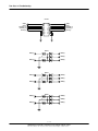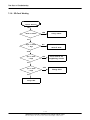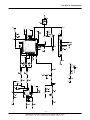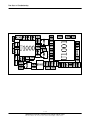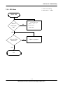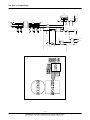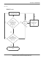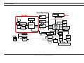
1
CDMA TELEPHONE
SCH-i830
CDMA TELEPHONE
CONTENTS
1.
General Introduction
2.
Circuit Description
3.
Installation
4.
NAM Programming
5.
Product Support Tools
6.
Test Procedure
7.
Flow Chart of Troubleshooting
8.
Exploded View/
Disassembly and Assembly Instructions
9.
Block Diagram
10.
Electrical Parts List
11.
PCB Diagrams
ⓒ Samsung Electronics Co.,Ltd. August. 2006
Printed in Korea.
This Service Manual is a property of Samsung Electronics Co.,Ltd.
Any unauthorized use of Manual can be punished under applicable
International and/or domestic law.
Code No.: GH68-12640A
BASIC.
1. General Introduction
1-1 General Instruction
The SCH-i830 enable mobile users to communicate 3G CDMA2000 1X, 1X EVDO 2G GSM service into
a single handset.
For CDMA/PCS mode, The SCH-i830 supports Release A of the CDMA2000 1X standard, offering data
rates of up to 307 kilobits per second (kbps) on both the forward and reverse links, along with
simultaneous voice and data services.
For The GSM/DCS/GPRS mode, The SCH-i830 supports voice service, data service and SMS in
EGSM900 and DCS1800.
So, The SCH-i830 may be the first PDA phone in the world that works on North American CDMA
networks and also GSM networks overseas. This stylish bar phone also supports a VGA color displays,
Bluetooth, SMS, Email, voice dialing, and airplane mode.
1-1
SAMSUNG Proprietary-Contents may change without notice
This Document can not be used without Samsung's authorization
General Introduction
1-2
SAMSUNG Proprietary-Contents may change without notice
This Document can not be used without Samsung's authorization
2. Circuit Description
2-1. Logic Section
2-1-1. Power Supply
For the POWER ON, the PHONE_ON pulse signal for 1 second from PDA turns on U900(PM6650)
The pin 29, 33, 35, 41, 52, 54, 65, 71, 83 of U900(PM6650) are the inputs of all regulators on the
phone. Simultaneously, MSM sends out PS_HOLD(logical HIGH) to turn on the pin 57 of
U900(PM6650) even after the PHONE_ON signal is released. For the POWER OFF, by pressing
POWER KEY of the phone application, the MSM output LOW on the PS_HOLD.
The regulated voltage(U900,VREG_MSMC, VRGE_MSME, VREG_MSMP ) is used in the digital part
of MSM
The regulated voltage(U900,VREG_MSMA) is used in the analog part of MSM.
The regulated volgtage(U900, VREG_RFTX)
is used in the TX RF
The regulated voltage(U900,VREG_RFRX) is used in the Rx RF part.
The regulated voltage(U900,VREG_TCXO) is used in the TCXO
The regulated Voltage(U900,VREG_SYNTH)
is used in the PLL part.
2-1-2. Logic Part
The logic part consists of internal CPU of MSM, Memory.
MOBILE SYSTEM MODEM(UCP800:MSM6500)
Industry standard ARM926EJ-S microprocessor is embedded. The MSM6500 chipset integrates
CDMA2000 1x and 1xEVDO service. The 1xEVDO solution can support High-speed peak data rates of
2.4Mbps on forward link and 153kbps on reverse link.
The MSM6500 device is offered in a 409 ball, 0.5mm pitch, CSP production package. Subsystems within
the MSM6500 device include a CDMA processor, a QDSP for voice compression, an ARM9TDMI
microprocessor. Also integrated in the MSM6500 device are analog functions such as an audio voice
codec, PLL, transmit DACS, ADCS, memories, USB controller, peripheral interfaces, and an enhanced
clock. It is one of the most important components of the CDMA cellular phone.
The interface circuitry consists of reset circuit, dual address/data bus and memory controls. The TCXO
clock of 19.2Mhz is used as the clock of SCH-i830 model.
MCP : FLASH ROM and SDRAM (UME802:K5D5657DCM)
MCP is consist of 256Mbit NAND FALSH and 256Mbit SDRAM. MCP is used to store the cellular
phone's executable program ,necessary data files and temporary data space and efs area is used to
store ESN, NAM information, telephone directory, SMS messages and other important information of the
phone. MCP is also used to execute the DMSS(Dual Mode Subscriber system) software.
2-1
SAMSUNG Proprietary-Contents may change without notice
This Document can not be used without Samsung's authorization
Circuit Description
Clock
CPU clock
: 19.2MHz. This clock signal from the TCXO
Sleep clock : 32.768KHz. This clock signal is used for sleep.
TCXO/N
: 19.2/N MHz. This clock source is used by various blocks of the MSM6500
device, such as the ARM9CORE, UARTs, general-purpose PDMs and
TCXO is also used by the MSM6500 device to produce CHIPX8.
USB clock : 48MHz. This clock signal is used to drive the USB interface
2-1-3. RF Interface Part
CDMA Data Interface
- TX_Q_P, TX_Q_N, TX_I_P, TX_I_N (UCP800) : Tx analog signal used during CDMA
- RX_I_P, RX_Q_P, RX_I_N, RX_Q_N (UCP800): RX analog signal used during CDMA
RF Interface
- TX : TX_AGC_ADJ(UCP100) is used to control the TX power,
PA_ON_PCS(UCP100) is used to control the PCS power amplifier and
PA_ON_CELL(UCP100) is used to control the CDMA power amplifier.
- RX : TRK_LO_ADJ(UCP100) is used to compensate the TCXO module.
2-1-4. Audio Part
The MSM6500 integrates an audio voiceband Codec into Mobile Station Modem.
The integrated Codec contains all of the required conversion and amplification stages for the
audio front end.
The Codec operates as a 13bit linear Codec with the transmit(TX) and
receive(RX) filters designed to meet ITU-TG.712 requirement. The CODEC contains the
software controller amplifier for both the receiving and transmitting sections. Also, the
vocoding schemes used will be 13kbps QCELP and 8Kbps EVRC. The QCELP vocoder is
based in the MSM internally.
Tx Audio Path
The voice signal from the microphone is inputted to the internal CODEC. The voice signal is then
amplified by the internal amplifier and is converted to PCM data to be outputted to the MSM as 13bit
data. This data is then processed by the MSM(UCP800)'s internal.
2-2
SAMSUNG Proprietary-Contents may change without notice
This Document can not be used without Samsung's authorization
Circuit Description
Rx Audio Path
The PCM data from the MSM(UCP800)'s internal is inputted to the internal CODEC and the data will be
decoded by the internal DAC and audio levels are adjusted by the amplifier. The final audio is then sent
to the audio receiver.
2-2. PCS Section
2-2-1. Receiver
LOW NOISE AMPLIFIER (U1000)
The low noise amplifier(It is included in FC7510:U1000) amplifies a weak signal received from
the base station to obtain the optimum signal level.
RF BAND PASS FILTER (F1001)
The RF BPF(F1001) passes only a specific frequency(1960±30 MHz) from the signal received from the
mobile station. The bandwidth is 60 MHz.
VOLTAGE CONTROLLED OSCILLATOR(VCO1000)
The VCO(VCO1000) generates the signal having center frequency 1715 ~ 1788MHz frequency
range with the voltage control. The PLL in RTR6300(U1102) controls this signal.
Frequency Synthesizer Circuit
The PLL(Phased Locked Loop) block consists of VC-TCXO(TCX1001), PLL in RTR6300 and
VCO(VCO1000). Input reference frequency is generated at VC-TCXO(TCX1001) and the RF
local signal is generated at VCO. PLL compares the two signals and generates the desired
signal with a preprogrammed counter which controls voltage.
VOLTAGE CONTROLLED TEMPERATURE COMPENSATED CRYSTAL OSCILLATOR (TCX1001)
The VC-TCXO (TCX1001) is a reference source of the frequency synthesizer. It provides 19.2MHz
reference frequency to PLL-IC. It is a voltage controlled temperature compensated crystal
oscillator having 19.2MHz ±2.5ppm frequency stability over all useful temperature range.
A correct frequency tuning is made by the control voltage.
l
2-3
SAMSUNG Proprietary-Contents may change without notice
This Document can not be used without Samsung's authorization
Circuit Description
2-2-2. Transmitter
Antenna(ANT1)
Antenna(ANT1) sends signal to the base station and receives the signal from the base station.
It is a multi-band Antenna and covers PCS band, CDMA band DCS band, GSM Tx band and GPS band.
RF Switch(U1201)
It(U1201) is used to switch the PCS path, the CDMA path the GPS path and the GSM path, The RF
signal pass through PCS path when PCS_SW is high.
PCS_SW, CDMA_SW, GPS_SW and GSM_SW are digital signals from MSM6500 via Decoder(U1200).
Duplexer(F1103)
Duplexer(F1103) allows to transmit only the signals within acceptable Tx
frequency range (1880 ± 30 MHz) through the antenna.
Power Amp(PAM1103)
Power amplifier module(PAM1103:CX77107) amplifies signals to be sent to the base station
through the antenna.
RF Band Pass Filter(Tx RF SAW Filter)
The RF BPF(F1101) pass only specific frequency(1880 ±30MHz) to send it to power
amp(PAM1103:CX77107).
Direct Conversion Transmitter(U1102)
The Direct Conversion Transmitter(U1102: RTR6300) allows the signal to be inputted to the
power amp(PAM1103) as a specified level from I, Q base band signals.
Automatic Gain Control Amp
The TX AGC amp (in RTR6300) controls gain of AGC to deliver power level needed at
driver amp. Its control voltage varies from 0.2V to 2.5V.
2-4
SAMSUNG Proprietary-Contents may change without notice
This Document can not be used without Samsung's authorization
Circuit Description
2-3. CDMA Section
2-3-1. Receiver
Low Noise Amplifier(U1000)
The low noise amplifier(It is included FC7510: U1000) amplifies a weak signal received from
the base station to obtain the optimum signal level.
RF Band Pass Filter(F1000)
The RF BPF(F1000) passes only a specific frequency(881.49±12.5 MHz) from the signal
received from the mobile station. The bandwidth is 25 MHz.
Voltage Controlled Oscillator(VCO1000)
The VCO(VCO1000) generates the signal having center frequency 1715 ~ 1788MHz frequency
range with the voltage control.
The PLL in RTR6300 controls this signal.
Frequency Synthesizer Circuit
The PLL(Phased Locked Loop) block consists of VC-TCXO(TCX1001), PLL in RTR6300 and
VCO(VCO1000). Input reference frequency is generated at VC-TCXO(TCX1001) and the RF
local signal is generated at VCO. PLL compares the two signals and generates the desired
signal with a preprogrammed counter which controls voltage.
VC-TCXO(TCX1001)
The VC-TCXO (TCX1001) is a reference source of the frequency synthesizer. It provides 19.2MHz
reference frequency to PLL-IC. It is a voltage controlled temperature compensated crystal
oscillator having 19.2MHz ±2.5ppm frequency stability over all useful temperature range.
A correct frequency tuning is made by the control voltage.
2-5
SAMSUNG Proprietary-Contents may change without notice
This Document can not be used without Samsung's authorization
Circuit Description
2-3-2. Transmitter
Antenna(ANT1)
Antenna(ANT1) sends signal to the base station and receives the signal from the base station.
It is a multi-band Antenna and covers PCS band, CDMA band DCS band, GSM Tx band and GPS band.
RF Switch(U1201)
It(U1201) is used to switch the PCS path, the CDMA path the GPS path and the GSM path, The RF
signal pass through PCS path when PCS_SW is high.
PCS_SW, CDMA_SW, GPS_SW and GSM_SW are digital signals from MSM6500 via Decoder(U1200).
Duplexer(DUF1107)
Duplexer(DUF1107) allows Rx frequency range(881.49 ±12.5 MHz) and Tx frequency range
(836.49 ±12.5 MHz) from the antenna to pass through LNA. It also matches LNA input in
receiving part and PAM(PAM1104:CX77105) output in transmitter part with the antenna.
Power Amp(PAM1104)
Power amplifier module(PAM1104:CX77105) amplifies signal to be sent to the base station
through the antenna.
RF Band Pass Filter(Tx RF SAW Filter)
The RF BPF(F901) pass only specific frequency(836.49 ±12.5MHz) to send it to power
amp(U903:CX77105).
Direct Conversion Transmitter(U1102)
The Direct Conversion Transmitter(U1102: RTR6300) allows the signal to be inputted to the
power amp(PAM1103) as a specified level from I, Q base band signals.
Automatic Gain Control Amp
The TX AGC amp in RTR6300 controls gain of AGC to deliver power level to be needed
at Driver amp. Its control voltage varies from 0.2V to 2.5V.
2-6
SAMSUNG Proprietary-Contents may change without notice
This Document can not be used without Samsung's authorization
Circuit Description
2-4. GSM/DCS Section
2-4-1. Receiver
Low Noise Amplifier(U1102)
The low noise amplifier(It is included in RTR6300 : U1102) amplifies a weak signal received from
the base station to obtain the optimum signal level.
Voltage Controlled Oscillator(VCO1000)
The VCO(VCO1000) generates the signal having center frequency 1715 ~ 1788MHz frequency
range with the voltage control.
The PLL in RFR6000 controls this signal.
Frequency Synthesizer Circuit
The PLL(Phased Locked Loop) block consists of VC-TCXO(TCX1001), PLL in RFR6000 and
VCO(VCO1000). Input reference frequency is generated at VC-TCXO(TCX1001) and the RF
local signal is generated at VCO. PLL compares the two signals and generates the desired
signal with a preprogrammed counter which controls voltage.
VC-TCXO(TCX1001)
The VC-TCXO (TCX1001) is a reference source of the frequency synthesizer. It provides 19.2MHz
reference frequency to PLL-IC. It is a voltage controlled temperature compensated crystal
oscillator having 19.2MHz ±2.5ppm frequency stability over all useful temperature range.
A correct frequency tuning is made by the control voltage.
2-7
SAMSUNG Proprietary-Contents may change without notice
This Document can not be used without Samsung's authorization
Circuit Description
2-4-2. Transmitter
Antenna(ANT1)
Antenna(ANT1) sends signal to the base station and receives the signal from the base station.
It covers GSM TX band, CDMA RTX band, GPS band, DCS RTX band.
RF Switch(U1201)
It(U902) is used to switch the PCS path, the CDMA path GSM/DCS path and the GPS path,
The RF signal pass through CDMA path when CELL_MODE is high.
PCS_MODE, CELL_MODE and GPS_MODE are digital signals from MSM6500 GPIO.
ASM(DUF1200)
Antenna Switch Module(DUF1200) allows Rx frequency range(881.49 ±12.5 MHz)
to come to the RX path and also allows Tx frequency range to go out to antenna
by switching between RX block and TX block..
Power Amp(PAM1101)
Power amplifier module(PAM1101) amplifies signal to be sent to the base station
through the antenna.
Up-Converter(VCO1101)
The up-converter(VCO1101) generate Tx RF signal by receiving the tune voltage
that correspond proper frequency.
2-8
SAMSUNG Proprietary-Contents may change without notice
This Document can not be used without Samsung's authorization
Circuit Description
2-5. GPS Section
Antenna
Antenna receives signal from GPS satellites.
It is a tri-band Antenna and covers GSM band, PCS band, CDMA band and GPS band.
RF Switch(U1201)
It(U1201:NJG1519KC1) is used to switch the GSM Path, PCS path, CDMA path and the GPS
path.
The RF signal pass through PCS path when PCS_SW is high The RF signal
pass through CDMA path when CDMA_SW is high. The RF signal pass through
GPS path when GPS_SW is high. The RF signal pass through GSM path when GSM_SW is high.
GSM_SW, PCS_SW, CDMA_SW and GPS_SW are digital signals from MSM6500 GPIO.
RF Band Pass Filter(F1002)
The RF BPF(F1002) passes only a specific frequency(1575.42±2 MHz) from the signal received
from the satellites. The bandwidth is 2 MHz.
Low Noise Amplifier(TR1001)
The low noise amplifier(TR1001) amplifies a weak signal received
from the satellites to obtain the optimum signal level.
Low Noise Amplifier(U1001)
The low noise amplifier(It is included in RFR6000 : U1001) amplifies a weak signal received
from the satellites to obtain the optimum signal level.
2-9
SAMSUNG Proprietary-Contents may change without notice
This Document can not be used without Samsung's authorization
Circuit Description
2-6. PDA PART
The PDA logic part consists of power supply part, MPU & memory part, LCD part, audio part
and all the peripherals.
2-6-1. POWER SUPPLY
When the battery is inserted to the handset,
VBAT makes VCC_BATT, VCORE14, VPLL13, VSRAM11 via U405(MAX1587) which is a CPU voltage
VCC30 via U405(MAX1587) which is CPU & peripheral voltage,
VCC28 via U414(MIC5219-2.8BML) which is a DPRAM voltage,
VLCD33 via U413(MIC2211-SSBML) which is a LCD logic voltage,
VBT30 via U416(MIC2211-PPBML) which is a Buletooth voltage.
VBAIS30 via U416(MIC2211-PPBML) which is a MIC vias voltage.
VBAT33 via U413MIC2211-SSBML) which is a backup battery charging voltage,
VSD30 via U410(MIC2212) which is a SD-Card voltage.
VCC30 makes VCC18 via U412(MIC2211-JGBML) which is a M-DOC voltage,
VDD30 makes VDD18 via U411(MIC2211-JGBML) which is a SDRAM voltage,
VLCD33 makes AVDD5V, VON, VOFF via U1000(MAX1779) which is LCD pannel voltage.
Backup Battery
The SPH-i830 has a back-up battery(ML1220) that stores data of SDRAM when the battery
removed or becomes low battery state that is below 3.1V.
The low battery state is checked by voltage detector or R3111Q311C(U400).
If the battery level is below 3.1V, nPOWER_FAIL signal is asserted. Then the backup DC/DC
converter(U405, MAX1676) output path is connected to VDD30 which is MPU, SDRAM voltage.
Backup battery supply main voltage or VDD30. If backup battery voltage is below 2V, discharging
path is disabled.
2-10
SAMSUNG Proprietary-Contents may change without notice
This Document can not be used without Samsung's authorization
Circuit Description
2-6-2. MPU & Memory part
MCP(UCP201:LVPXA272FC5520)
● ARM Architecture
● Built in Memory Controller, LCD Controller, AC97 Controller and MMC Controller
● Intel® PXA272 processor with 64 Mbytes of Intel StrataFlash® memory
Flash memory is used to store the PDA executable program and necessary data files.
● Clock and Power Controllers
● It has a variety of different system peripherals and controls all the peripheral circuitry.
● 13x13mm VFBGA package
NAND FLASH Memory(UME301:MD4832D512)
High capacity: single die - 512Mbit (64MB)
Nand Flash memory is used to user data files.
SDRAM Memory(UME305:K4S51323PF)
Samsung CMOS technology
●64MByte capacity Mobile Synchronous Dynamic RAM.
●It is used as a application program execution space, temporary data space to store the internal flag
information, timer data, and user data files.
DPRAM Memory(UME300:IDT70P248L55)
4Kx16bit dual port RAM
●It is accessed by Phone and PDA, but not accessed simultaneously.
●Generally, Instructions and data used by Phone and PDA are stored.
2-6-3. LCD part
PXA272 has a LCD controller.
LCD module
●a transflective type color active matrix TFT
●It is composed of a TFT LCD module(TFT LCD panel, driver ICs), a Backlight unit and
a touch screen panel.
●The resolution of 2.8inch contains 240x320 pixels and can display 65K colors.
2-11
SAMSUNG Proprietary-Contents may change without notice
This Document can not be used without Samsung's authorization
Circuit Description
2-6-4. Audio part
PDA plays audio files via WM9712 and the voice of the phone is connected to the WM9712.
WM9712(U400)
The WM9712 is a high quality stereo codec with an integrated touch screen controller.
Interfaced to PXA272 via AC'97 protocol.
● AC'97 Rev 2.2 specification
● headphone outputs
● a complete 4-wire touch screen controller
2-6-5. Wireless Part
—
Bluetooth
Antenna
Antenna receives signal from AP(Access Point) or other devices.
It is a ISM(industrial, Scientific, Medical frequencies) Band Antenna that covers only 2.4 GHz.
Module
The Bluetooth Module which uses CSR's BC02-Audio is manufactured by SEMCO. It only supports
802.15 Specification(Bluetooth Specification 1.1) and communicates with CPU through UART Interface.
The data throughput is up to 1 Mbps in the abstractly but typically supports 723 / 57.6 Kbps in an
asynchronous mode and 432.6 kbps in a synchronous mode.
Modulation method is FHSS(Frequency hopping spread spectrum) and it hops 1600 times a second.
Its channel spacing is 1MHz and bandwidth is 1MHz.
2-12
SAMSUNG Proprietary-Contents may change without notice
This Document can not be used without Samsung's authorization
Circuit Description
2-6-6. All the Peripherals
Memory card
The MultiMediaCard Controller on the Intel PXA272 can communicate with either:
● a MultiMediaCard (MMC)
● a Secure Digital (SD) Memory Card
● a Secure Digital I/O (SDIO) Card
IrDA(U200:HSDL-3003)
● IrDA Data Compliant 115.2kbit/s with Remote Control Transmission Infrared Transceiver.
● a small form factor single enhanced infrared transceiver module that provides
the combination of interface between logic and IR signals for through-air, serial,
half-duplex IR data link, and IR remote control transmission operating at 940nm
for universal remote control applications.
USB
There is a USB Client in the Phone part and PDA part each.
The USB signals are switched to the interface connector via MUX(U604, MAX4636).
The USB interface of the Phone part is used for downloading and data service.
The USB of the PDA part is used for downloading user files and application programs by Active Sync to
PC.
UART
There is a UART port in the Phone part and PDA part each.
The UART signals are switched to the via the MUX(U601, MAX4684).
KEYPAD
For user interface, a keypad is used for function. For key recognition, a key matrix is set up using
signals KBC_(0)~(6) and KBR_(0)~(7) of the PXA272.
2-13
SAMSUNG Proprietary-Contents may change without notice
This Document can not be used without Samsung's authorization
Circuit Description
2-14
SAMSUNG Proprietary-Contents may change without notice
This Document can not be used without Samsung's authorization
3. Installation
3-1. Installing and Removing the Battery
To install
To remove
1. Place the battery on the back of the phone,
Push the battery release latch, then slide the
making sure the plastic tabs are aligned with the
battery toward the bottom end of the phone
corresponding holes in the phone
2. Gently push the battery up until it snaps into
place
3-2. Using the Desktop Charger
1. Plug the AC cord from the charger into the
◇ A red light on the charger lets you know the
electrical outlet.
battery is charging.
2. Insert the phone into the slot.
◇ A green light lets you know that the battery is
at least 90 percent charged.
◇ A orange light indicates that the battery is
operating at a temperature that is too high or
low, or that the charger is not plugged in
correctly. Please check the charger and the
battery.
Specifications using DTC (Desktop Charger)
Standard Battery
Extended Battery
(Li-ion, 1100mAh)
(Li-ion, 1700mAh)
Charging
< 5 hours
< 5 hours
SEC Code
GH43-02529A
GH43-02518A
Battery Type
3-1
SAMSUNG Proprietary-Contents may change without notice
This Document can not be used without Samsung's authorization
Installation
3-2
SAMSUNG Proprietary-Contents may change without notice
This Document can not be used without Samsung's authorization
4. NAM Programming
4.1 Programming of MDN and MSID
MDN and MSID can be programmed as follows:
Notes:
Press ##MSL#(ex: ##222222#) to enter Service Menu.
1) To view press View or to edit press Edit.
2) While editing, press OK to save. When OK is pressed after editing MDN, MSID will change to
all 0’s. Need to input a valid MSID and press OK to save the changes.
3) Press Done to save and exit programming
MDN and MSID Setting Flow:
LCD Display
change
Function
Service Menu
Phone Number
Enter the number
MSID
Enter the number
This screen allows you to view and modify the
phone number(MDN).
This screen allows you to view and modify the
Mobile Station ID Number(MIN).
4.2 Programming of the NAM parameters (Advanced)
NAM parameters can be programmed as follows:
Notes:
Press ##3282#. Select ‘Advanced’ button.
1) Screen will prompt for entering SVC code.
2) Enter the 6-digit MSL(ex: 222222) and then press OK.
3) To view press Advanced View or to edit press Advanced Edit.
4) Choose up/down to choose and press OK to save.
5) Some parameters press left/right key to change value.
6) Press Done to save and exit programming
4-1
SAMSUNG Proprietary-Contents may change without notice
This Document can not be used without Samsung's authorization
NAM Programming
NAM SETTING FLOW:
LCD Display
change
Function
Service Menu
This screen allows you to view and modify the
Home SID (4139)
Enter the number
Home NID (65535)
Enter the number
This screen allows you to view and modify the
home Network ID (NID).
MCC (310)
Enter the number
The MCC screen allows you to view and modify
the mobile country code.
MNC (00)
Enter the number
The MNC screen allows you to view and modify
the mobile network code.
ACCOLC
Enter the number
The ACCOLC screen allows you to view and modify
the access overload class.
CDMA Home Reg (YES)
Toggle Yes or No by
press ← → and
select by press enter key
Home SID Registration.
CDMA fSID Reg (YES)
Toggle Yes or No by
press ← → and
select by press enter key
Foreign SID Registration.
CDMA fNID Reg (YES)
Toggle Yes or No by
press ← → and
select by press enter key
Foreign NID Registration.
ESN (Hexa Number)
Cannot change
Electronic Serial Number of the phone is displayed.
P_REV (6)
Cannot change
Protocol Revision of the phone is displayed.
VOCODER (EVRC)
Toggle the item by
press ← → and
select by press enter key
Select vocoder option between EVRC and 13K
Vocoder.
SCM (00101010)
Cannot change
Station Class Mark of the phone is displayed.
Lock Code
Enter the number
This screen allows you to view and modify the
lock code.
SLOT MODE (YES)
Toggle Yes or No by
press ← → and
select by press enter key
SLOT CYCLE INDEX (2)
Enter the number
home system ID (SID).
This screen allows you to view and modify the
slotted mode.
This screen allows you to view and modify the
slot cycle index.
4-2
SAMSUNG Proprietary-Contents may change without notice
This Document can not be used without Samsung's authorization
5. Product Support Tools
5-1. General
IMPORTANT INFORMATION
Purpose
The Product Support Tool (PST) offers you the ability to interface with the SAMSUNG mobile phone
using a PC. With this tool you can program the phones network system requirements and functionality,
data, and download software upgrades. This document supports UniPST(Universal Product Support Tool).
EQUIPMENT REQUIRED
Make sure you have the following equipment setup:
1. Minimum PC configuration: 586 CPU, 64MB RAM, Windows2000/XP and above, 5MB of disk space
free for software upgrade.
2. PST Software with appropriate cable (USB Cable for SAMSUNG mobile phone).
3. USB Port.
4. Power Supply (4.3 V) or Battery.
INSTALLATION
1. Insert the SCH-i830 CDROM into your CD-Rom drive.
2. Run the file explorer and run the Setup.exe file.
3. After UniPST is installed on a computer, connect the phone, cable, and PC .
5-1
SAMSUNG Proprietary-Contents may change without notice
This Document can not be used without Samsung's authorization
Product Support Tools
5-2. PST (Product Support Tool)
5-2-1. Getting Started
MAIN MENU SCREEN
1. Double Click on your "UniPst" on UniPst-Sprint folder.
2. Select SCH-i830
The Main Menu Screen shows the basic tasks that are available.
CAUTION: DO NOT attempt to program phone with a low battery.
PST SETUP
UniPst supports SAMSUNG Mobile phone. You can select virtual USB port.
5-2-2. Operation Procedure
Service Programming
Before start service programming, you must change phone mode of SCH-i830
The Service Programming screens enable you to set and change the service activation parameters of the
phones.
Read Data from File
Click "Open mmc" icon to select the name of a file whose extension is "mmc". The values will be read
from the named file, and will initialize the parameter values seen on the Service programming screen
Read Data from Phone
Click Read from the Phone icon to upload the current programmable parameters of the phone. The
values are read from the phone, so the phone must have the power ON and be properly connected
to the PST.
NOTE: To actually view the data you need to go to the Edit Items screens.
Edit Items
Click this icon to edit Number Assignment Module (NAM) items or UI items.
1. General : Slot Cycle Index, Service Code
2. NAM1
Save Data to File
Click this icon to save the current parameters to a file. Once you enter a filename, Click <OK> button to
write all current parameters to that file. This way the same information can be downloaded into multiple
phones.
5-2
SAMSUNG Proprietary-Contents may change without notice
This Document can not be used without Samsung's authorization
Product Support Tools
Write to Phone
Click this icon to write the selected parameter values to the phone. Writing the selected values to the
phone may take up to a minute. If there are dependencies in a field you can make all the changes in
the proper fields and download the information all together.
If you intend to use this write to Phone? feature, it is recommended that you do a "Read Data from
Phone" first, and then make the changes, so that nothing gets inadvertently overwritten.
NOTE: DO NOT TOUCH THE PHONE WHILE WRITING IS IN PROGRESS.
Software Download
―
Performing Software Upgrade
z
HW version : 1.2
z
SW version : ZH21 or later
z
Please use SamsungPST FW Setup1.0.002_MSI 2ndEdition and
PSTI830.dll ( Universal PST For Sprint 1.723 - [SCH-i830] or higher)
When the user downloads the S/W on the SCH-i830 device the user may use external power removing
battery from the device or a fully charged battery.
Install USB drivers (use MCCI USB driver version 4.16)
For data call test and downloading new s/w,
install two setup programs which located in the / USB_Driver directory.
A.
SAMSUNG USB Modem driver_V4.16.zip (Phone USB)
B.
MSASYNC.EXE
(Active sync 4.1, it also install PDA USB driver)
FIG 1. Active sync connection setting
From fig 1. Showing above is the correct configuration of active sync for data call and downloading.
When the user downloads the s/w on the i830 device the user may use travel charger, fully charged battery
or JIG ( refer to 15) connections.
5-3
SAMSUNG Proprietary-Contents may change without notice
This Document can not be used without Samsung's authorization
Product Support Tools
IMPORTANT :
Please proceed following steps prior to
ⅰDownload the PRL and ERI
ⅱ Read/Write the settings
ⅲ Download software (.img)
1. Start -> Settings -> Choose "System tab" -> Data Connection
2. Choose "As the modem through USB". Press "ok": USB path will be changed to phone.
3. Now the hand set is ready to download, please follow the steps below.
A. Make sure that USB DATA cable plugged into the user PC properly.
B. Run the "UniPst" and select SCH-i830. Press "RUN".
C. Choose "Download Mode" which is below main menu.
D. Go to "Setup" > "COMM Setting". Make sure that correct COM port is selected.
E. Go to "File" > "Open Bin" to locate image file (For example, i830WM5.1.2S.ZH21.img) to download.
D. Click "Phone + PDA" icon to download both phone and PDA images.
(If the user need to download “PHONE ONLY” or “PDA ONLY” the user must pick the re-set hole for
more than 3 seconds.)
E. Select "OK" in next below message
"Is Current CDMA USB Modem Port X ?"
F. Select "OK" again, and then do hard reset the phone as described in the dialog window.
G. After downloading is complete, please verify handset.
Press Start Menu and go to "Start" >"Settings" > "System" tab > "Phone Info" to make sure that
appropriate PDA and phone versions are shown.
Trouble shooting for the following message:
Ø “Error in changing USB DM”
1. TEST MODE ( 6 5 4 8 # 0 * 4 5 6 8 0 )
2. Press 001
3. Press 100
4. Change Port map to U1_HFK USB_DS by using up, down arrow
5. Press enter
6. Press 002
7. Change USB path “ as the modem through USB” by (Start -> Settings -> Choose "System
tab" -> Data Connection)
5-4
SAMSUNG Proprietary-Contents may change without notice
This Document can not be used without Samsung's authorization
7. Flow Chart of TroubleShooting
7-1. Logic Section
7-1-1. Power On
PDA Part
Insert Power
NG
2pin in U400
NO
Change Batt.
> 3.4V
YES
4pin in U401
NO
Check U401 &
= High
Neighboring Circuits
YES
3pin in U405
NO
Check U405 &
= High
Neighboring Circuits
YES
34,35pin IN U405
NO
= High
Check U429,UCP201
& Neighboring Circuits
YES
In U405
NO
4pin = 3.0V , 23pin = 1.3V
Check U401 &
Neighboring Circuits
25pin = 1.1V , 33pin = 1.4v
YES
Check
Other Power Circuit
7-1
SAMSUNG Proprietary-Contents may change without notice
This Document can not be used without Samsung's authorization
Flow Chart of Troubleshooting
VBAT
VCC_BATT
C401
U401
VCC
1
2
U400
1
2
OUT
GND
VDD
NC
4
4
nPOWER_FAIL
Y
A
GND
3
5
B
3
C403
R408
C404
VCC_BATT
C405
1
nPOWER_FAIL
INA
VCC
5
2
3
nBATT_FAIL
INB
4
OUTY
VCC30
VCC30
GND
VBAT
VCC_BATT
VCC30
nBATT_FAULT
U404
R410
R411
C408
C409
C410
C419
C420
C411
TP403
nVCC_FAULT
TP402
C412
V_BKBT
R414
17
RAMP
18
GND
19
REF
BYP
43
42
ON3
FB3
30 _RSO
SRAD
29
PV3
27 LX3
28
PG3
V5
25
26
IN45
ON45
V4
23
24
21
22
ON2
CC3
_MR
41
40
39
38
37
NC
NC
PG1
ON1
R426
L401
36
15
16
IN
20
U405
PG2
LX1
35
PV1
SYS_EN
VCORE14
PWR_EN
R431
C422
VCC_BATT
VCC_BATT
C423
R432
VCC_BATT
PWR_EN
5
VCC
C425
C424
C426
C427
B
4 Y
R433
R434
A
GND
3
VPLL13
nRESET_IN
C431
VBAT
C432
VCC30
C433
VCORE14
L403
VBAT
nCHARGE_OFF
U408
1
2
C444
C438
VSRAM11
OUT
GND
VDD
NC
C421
R429
34
R427
VCC30
PWR_EN
33
13
LX2
_SLP
C413
R425
32
CC1
PWM3
PV2
VBAT
R422
31
2
1
FB1
4
3
BKBT
V7
V1
5
8
10
6
V2
FB2
CC2
SLPIN
GND
SDA
14
12
PWR_SDA
PK
SCL
11
R424
9
VBAT
7
R419
PWR_SCL
VBAT
TA439
TA440
4
3
C443
6.3V
7-2
SAMSUNG Proprietary-Contents may change without notice
This Document can not be used without Samsung's authorization
1
2
U409
nGPIO_RESET
nPOWER
Flow Chart of Troubleshooting
7-3
SAMSUNG Proprietary-Contents may change without notice
This Document can not be used without Samsung's authorization
Flow Chart of Troubleshooting
PHONE Part
Phone ON
NG
2pin in U302
YES
= High
Check UME300 &
Neighboring Circuits
NO
4pin in U803
NO
= High
1pin in U803
NO
= High
Check U900
Neighboring
Circuits
YES
YES
Check U803
31pin in U900
NO
=High
Check UCP800 &
Neighboring Circuits
YES
Output Powers
in U405 OK?
NO
Check U900
Neighboring
Circuits
YES
Check UCP800 & OSC200
Neighboring Circuits
7-4
SAMSUNG Proprietary-Contents may change without notice
This Document can not be used without Samsung's authorization
Flow Chart of Troubleshooting
VCC28
C327
U302
1
2
PHONE_ACTIVE
3
R324
NC
VCC28
VCC
C328
5
R323
5
IN
GND OUT
VCC28
1
4
DPRAM_CS_N
2
VCC
B
Y 4
A
GND
3
U303
7-5
SAMSUNG Proprietary-Contents may change without notice
This Document can not be used without Samsung's authorization
nCS_DPRAM
Flow Chart of Troubleshooting
VBAT
TR900
V_IN
< PHONE Power Management IC >
56
VBAT_PM6650
G
3
4
12
SS
L900
L901
TA900
C901
ZD900
R900
R901
TR901
R902
R903
VREG_MSMC
R905
V_IN
9PF
C902
R907
R906
3
1
VBAT_PM6650
C903
9PF
2
TR902
OSC900
CC4V-T1
2
TP900
TP901
TP902
C904
1
TP903
SLEEP_XTAL_IN
TCXO
TCXO_EN
TCXO_OUT
34
R913
C905
TP904
R910
AMUX_OUT
GSM_PA_PWR_CTL_REF
< USIM SOCKET >
D901
R918
C907
3
R914
0
PHONE_D+
PHONE_D-
1
R915
R916
nPMIC_RESET
0
SIM_IO
USIM_IO
SIM_CLK
USIM_CLK
SIM_RST
USIM_RST
C924
C925
C923
C927
C926
C928
PM_SBDT
PM_SBCK
PM_SBST
PM_INT_N
C929
1
44
46
45
58
55
53
70
72
82
80
ADC_BYP
XTAL_IN
XTAL_OUT
SLEEP_CLK
TCXO_IN
TCXO_EN
TCXO_OUT
AMUX_IN1
AMUX_IN2
AMUX_OUT
REF_OUT
13
17
19
11
18
20
24
57
66
68
9
30
26
34
38
40
43
47
49
51
59
USB_OE_N
USB_DAT
USB_SE0
USB_ID
USB_D_P
USB_D_M
KPDPWR_N
PS_HOLD
CBL1PWR_N
CBL0PWR_N
PON_RESET_N
RUIM_M_IO
RUIM_IO
RUIM_M_CLK
RUIM_CLK
RUIM_M_RST
RUIM_RST
SBDT
SBCK
SBST
MSM_INT_N
1
3
85
R920
R919
VCHG
USB_VBUS
ISNS_P
ISNS_M
CHG_CTL_N
USB_CTL_N
VBAT
VCOIN
BAT_FET_N
VBACKUP
GND
R917
1 1
6 6
5
2 2
5
3 3
4 4
G G G G
10 9 8 7
VREG_USIM
USB_OE_N
USB_DAT
USB_SEO
2
PS_HOLD
IF_CON_SENSE
SIM900
VSW_5V
VREG_5V
VSW_PA
VREG_PA
VSW_MSMC
VREG_MSMC
VSW_MSME
VREG_MSME
VREG_USB
VREG_MMC
VREG_RUIM
VREG_MSMP
VREG_MSMA
VREG_WLAN
VREG_RFRX2
VREG_RFRX1
VREG_RFTX
VREG_SYNT
VREG_TCXO
REF_ISET
REF_BYP
REF_GND
14
12
27
28
31
32
37
36
10
39
42
50
56
64
67
69
73
81
84
61
63
62
FLSH_DRV_N
GP1_DRV_N
LCD_DRV_N
KPD_DRV_N
VIB_DRV_N
SPKR_IN_P
SPKR_IN_M
SPKR_OUT_P
SPKR_OUT_M
SPKR_BYP
VDD_SPKR
8
21
22
23
25
76
78
75
79
74
77
VDD_PA
VDD_MSMC
VDD_MSME
VDD_RUIM
VDD_MSM
VDD_ANA
VDD_WLAN
VDD_RF
VDD_MAIN
29
33
35
41
52
54
65
71
83
VREG_USIM
VREG_MSME
R912
V_IN
C908
C909
C910
C941
R921
V_IN
C935
C936
C931
C930
C932
C933
C934
C937
VCC_BATT
VCC
4
2 IN
4
OUT
3
GND
PS_HOLD
C940
U901
VREG_MSMP
C864
U803
VCC
1 INA
nMSM_RST
2
5
GND
3
nPMIC_RESET
INB
OUTY
4
RESIN_N
RFU_1
W9
PWR_CAP_3_GPIO8
PWR_OUT
D20
E16
PWR_CAP_1_GPIO6
PWR_CAP_2_GPIO7
E18
D18
C19
TXTAL_IN
TXTAL_OUT
PWR_CAP_0_GPIO5
R862
A17
C247
C251
1
C250
C252
C253
2
OUTY
B17
INB
PHONE_ON
5
GND
3
VREG_TCXO
R911
VCC5
4
1 INA
2
VREG_SYNT
C906
U902
PS_HOLD_P
VREG_RFTX
R909
VCC_BATT
nBATT_FAULT
VREG_RFRX
L903
C938
1NC
VREG_MSMA
R908
TR903
C939
VREG_MSMP
L902
2
3
PS_HOLD
2
16
3
5
4
15
6
60
7
48
NC
NC
R904
86
87
3D
U900
IF_CON_SENSE
VBUS_PM6650
VBUS_PM6650
1
G
2S
VBUS
OSC200
7-6
SAMSUNG Proprietary-Contents may change without notice
This Document can not be used without Samsung's authorization
C918
C911 C912
C913
C919 C920
C921 C922
C914 C915
C916 C917
Flow Chart of Troubleshooting
7-7
SAMSUNG Proprietary-Contents may change without notice
This Document can not be used without Samsung's authorization
Flow Chart of Troubleshooting
7-1-2. LCD Working
Insert Power
NG
LCD Display
9pin in U413
NO
3pin in U413
NO
Change
= High?
= High?
OK?
NO
PBA
YES
YES
Change U413
4pin in U1000
NO
Check LCD TOP FPCB,
= High?
Slide FPCB
YES
YES
1pin in D1001 = 4~5V?
NO
2pin in D1003 = 17~18V?
Check U1000 &
neighboring circuits
1pin in D1002 = -8~9V?
YES
Check
LCD TOP FPCB & LCD
Back Light
NO
OK?
4,5pin in U1001
NO
Check LCD TOP FPCB,
= High?
Slide FPCB
YES
1pin in U1001
YES
Check U1001 &
NO
neighboring circuits
= 12V?
YES
Check
LCD TOP FPCB & LCD
TSP
OK?
NO
When touch screen
46pin in U900
NO
= High?
YES
Check
LCD TOP FPCB ,
Slide FPCB & LCD
ZD603
Check ZD603,UCD500 &
neighboring circuits
7-8
SAMSUNG Proprietary-Contents may change without notice
This Document can not be used without Samsung's authorization
Flow Chart of Troubleshooting
VBAT33
VBAT
VLCD33
U413
nCHARGE_OFF
LCD_ON
11 VIN
VOUT1
2 EN1
VOUT2 9
0
3 EN2
N/C 8
4 CBYP
N/C 7
GND 6
GND
GND
GND
GND
GND
GND
5 N/C
C457
C458
C453
11 12 13 1415 16
C454
AVDD5
C1000
AVDD5
V_LCD33
R1000
VDD5
D1000
L1000
C1001
R1001
C1002
C1003
R1002
VCC30_SUB
R1003
C1004
L1002
U1000
U1001
6
5
4
PWM_BLED_SUB
SW
VOUT
VIN
GND
CTRL
FB
1
LED+
2
R1004
3
LEDR1005
C1013
C1011
R1006
15
3
14
C1007
13
D1001
1
12
11
10
C1010
9
C1012
MAX1779EUE
D1002
C1014 C1015
2
C1005
1 _RDY TGND 16
2 FB
LX
3
INTG PGND
4
IN
SUPP
5
GND DRVP
6
REF
SUPN
7
FBP
DRVN
8
FBN _SHDN
C1006
R1007
1
1
3
3
2
2
D1003
VON
R1008
VOFF
VON15
C1016 C1017
VOFF9
R1009
100K
R555
40 HPGND
HPOUTR
MIC2
41 HPOUTR
42
AGND2
43
HPVDD
44
GPIO1
45
GPIO2/IRQ
46
GPIO3/PENDOWN
47
GPIO4/ADA/MASK
48
GPIO5/SPDIF_OUT
49 GND
50 GND
51 GND
MIC1
UCD500
PEN_DETECT
PHONE
PCBEEP
TPGND
Y-/BL
X-/TL
Y+/TR
PHONE_MIC_JMP
22 R511
C524
21
MIC
20
PHONE_SPK
R518
19
18
17
16
15
X+/BR 14
TA529
C531
TSMY
TSMX
TSPY
TSPX
TPVDD 13
ZD603
TSPX
1
2
TSMX
34
IO
6
CLOCK
GND
NC
SIM VCC
TSMY
5
TSPY
7-9
SAMSUNG Proprietary-Contents may change without notice
This Document can not be used without Samsung's authorization
Flow Chart of Troubleshooting
7-1-3. Audio Working
Speaker Working
Operate Speaker
NG
SPK Contact Pad
in Side FPCB
YES
Change SPK
Signal ON?
NO
A3,C3 pin in U505,
YES
A3,C3 pin in U506
Check Side FPCB &
HDC 600
Signal ON?
NO
2,10pin in U503
YES
Check U505,U506
& Neighboring Circuits
Signal ON?
NO
4,8pin in U503
YES
35,36pin in UCD500
= High
NO
YES
Signal ON?
NO
Check UCD500
& Neighboring Circuits
7-10
SAMSUNG Proprietary-Contents may change without notice
This Document can not be used without Samsung's authorization
Change U503
Flow Chart of Troubleshooting
HDC600
11
3 3
55
7 7
99
11 11
13 13
15 15
KBR(0)
KBC(0)
SPEAKER_R+
SPEAKER_RMOTOR_R
2
4
6
8
10
12
14
16
ZD602
RCVOUT
LED_G
2
4
6
8
10
12
14
16
KBR(1)
KBC(1)
SPEAKER_L+
SPEAKER_LMOTOR_L
1
6
HPOUTL
2
5
LED_R
3
4
LED_B
7-11
SAMSUNG Proprietary-Contents may change without notice
This Document can not be used without Samsung's authorization
Flow Chart of Troubleshooting
Reciever Working
Operate Reciever
NG
RCV Soldering Pad
in LCD TIP FPCB
YES
Change RCV
Signal ON?
NO
37,39pin in UDC500
Signal ON?
YES
Check LCD TOP FPCB,
Slide FPCB & ZD602
NO
Check UDC500
& Neighboring Circuits
7-12
SAMSUNG Proprietary-Contents may change without notice
This Document can not be used without Samsung's authorization
Flow Chart of Troubleshooting
Mic Working
Operate MIC
NG
4pin in U507
NO
Signal ON?
Check D501 &
Change MIC
YES
5pin in U507
NO
Signal ON?
1pin in U507
NO
= Low?
Check U508 &
Neighboring Circuits
YES
YES
Change U507
3pin in U501
Signal ON?
NO
4pin in U501
YES
= High?
NO
YES
Check UDC500
& Neighboring Circuits
7-13
SAMSUNG Proprietary-Contents may change without notice
This Document can not be used without Samsung's authorization
Change U501
Flow Chart of Troubleshooting
Hands-Free Stereo Headset Working
Hands-Free
Stereo Headset
SPK , MIC
YES
& Button
NO
10pin in U416
= High?
All NG?
Change
Neighboring Circuits
U416
YES
1pin in U508
YES
= High?
NG?
Change
PBA
YES
Check EAR500 &
NO
NO
= High?
YES
Button
2pin in U416
Change PBA
NO
NO
Check EAR500, U508 &
Neighboring Circuits
MIC
YES
NG?
NO
6pin in U507
Signal ON?
Check EAR500 &
Neighboring Circuits
YES
NO
5pin in U507
Signal ON?
NO
= High?
NG?
YES
Check U501, U508
Check U508 &
& Neighboring Circuits
Neighboring Circuits
39,41pin
in UDC500
Change U507
NO
YES
SPK
YES
7pin in U508
YES
10pin in U501
YES
Signal ON?
Signal ON?
NO
Check UDC500, U501
& Neighboring Circuits
7-14
SAMSUNG Proprietary-Contents may change without notice
This Document can not be used without Samsung's authorization
Check U508 &
Neighboring Circuits
Flow Chart of Troubleshooting
7-1-4. KEY Working
Press KEY
NG
Volume key or
Voice Recoding key
YES
Break a
YES
Side Key FPCB
NG?
Change
Side Key FPCB
NO
Check HDC600,ZD604 &
NO
KEY Metrix connection circuits
Application key
or Navigation key
Break a
YES
YES
LCD Top FPCB
LCD Top FPCB
or Slide FPCB
or Slide FPCB
NG?
Change
NO
NO
Check ZD601 &
KEY Metrix connection circuits
Qwerty key or
Voice Signal key
YES
Check ZD718,ZD719,ZD720 &
KEY Metrix connection circuits
NG?
NO
Power key
or Lock key
YES
YES
Break a
SW700
NG?
Change
SW700
NO
SW700
Check SW700
& neighboring circuits
7-15
SAMSUNG Proprietary-Contents may change without notice
This Document can not be used without Samsung's authorization
Flow Chart of Troubleshooting
HDC600
11
3 3
55
7 7
99
11 11
13 13
15 15
KBR(0)
KBC(0)
SPEAKER_R+
SPEAKER_RMOTOR_R
2
4
6
8
10
12
14
16
2
4
6
8
10
12
14
16
KBR(1)
KBC(1)
SPEAKER_L+
SPEAKER_LMOTOR_L
ZD718
KBC(0)
KBC(3)
1
6
KBC(1)
2
5
KBC(2)
3
4
KBC(4)
1
6
KBC(6)
2
5
KBR(1)
3
4
KBR(3)
1
6
KBR(5)
2
5
KBR(6)
3
4
KBR(7)
ZD719
KBC(5)
KBR(2)
ZD720
KBR(0)
KBR(4)
7-16
SAMSUNG Proprietary-Contents may change without notice
This Document can not be used without Samsung's authorization
Flow Chart of Troubleshooting
7-17
SAMSUNG Proprietary-Contents may change without notice
This Document can not be used without Samsung's authorization
Flow Chart of Troubleshooting
7-1-5. Vibrator Working
Operate Vibrator
NG
SPK Contact Pad
in Side FPCB
YES
Change SPK
Signal ON?
NO
A3,C3 pin in U505,
A3,C3 pin in U506
Signal ON?
YES
Check Side FPCB &
HDC600
NO
2,10pin in U503
YES
Signal ON?
Check U505,U506
& Neighboring Circuits
NO
4,8pin in U503
= High
YES
35,36pin in
UCD500
YES
Signal ON?
NO
NO
Check UCD500
& Neighboring Circuits
7-18
SAMSUNG Proprietary-Contents may change without notice
This Document can not be used without Samsung's authorization
Change U503
Flow Chart of Troubleshooting
AVCC30 VBAT
L501
R552
C551
C552
U505
A2
B1
VDD VSS VOM A3
C554
R539
C555
R540
A1 VIP
C1 VIM
SPEAKER_R+
PVSS B3
C2 EN
B2 PVDD
NC
NC
RSPKOUT
VOP C3
SPEAKER_R-
12
AMP_EN
AVCC30 VBAT
L502
R553
C557
C558
100NF
U506
A2
B1
VDD VSS VOM A3
C561
R545
C563
R546
A1 VIP
C1 VIM
SPEAKER_L+
PVSS B3
C2 EN
B2 PVDD
NC
NC
LSPKOUT
VOP C3
12
AMP_EN
7-19
SAMSUNG Proprietary-Contents may change without notice
This Document can not be used without Samsung's authorization
SPEAKER_L-
Flow Chart of Troubleshooting
7-1-6. SD-Card Working
Insert SD-Card &
Operate SD-Card
NG
Break a CD702?
YES
Change CD702
NO
12pin in CD702
NO
= High
Check
CD702 & R746
YES
4pin in U410
YES
= High
Check CD702 & it's
neighboring circuits
NO
1pin in U410
YES
Change U410
= High
NO
Change PBA
7-20
SAMSUNG Proprietary-Contents may change without notice
This Document can not be used without Samsung's authorization
Flow Chart of Troubleshooting
VBAT
1
VSD_ON
VSD30
U410
EN
2
BYP
NC
GND
3 IN
OUT
GND
6
5
4
7
C430
VSD30
VSD30
C428
C429
VCC30
VCC18
C705
R747
R746
R745
R744
R743
R742
C707
R741
TA706
CD702
1
2
3
4
5
6
7
8
9
WPS/W
COMMON
CDS/W
GND
GND
GND
1
2
3
4
5
6
7
8
9
SD_DAT3
SD_CMD
SD_CLK
SD_DAT0
SD_DAT1
SD_DAT2
nSD_WP
10
11
12
13
14
15
SD_DETECT
R759
C713
SD_CARD
7-21
SAMSUNG Proprietary-Contents may change without notice
This Document can not be used without Samsung's authorization
Flow Chart of Troubleshooting
7-22
SAMSUNG Proprietary-Contents may change without notice
This Document can not be used without Samsung's authorization
Flow Chart of Troubleshooting
7-1-7. IrDA Working
Operate IrDA
NG
Break a
YES
LCD Top FPCB
Change
LCD TOP FPCB
NG
Break a
YES
Change
Slide FPCB
Slide FPCB
NG
Check ZD 605, ZD604 &
SLC601
7-23
SAMSUNG Proprietary-Contents may change without notice
This Document can not be used without Samsung's authorization
Flow Chart of Troubleshooting
ZD605
1
IRDA_TX
2
3
IRDA_RX
IO
6
LCD_MCLK
CLOCK
GND
NC
5
4
SIM VCC
LCD_DE
ZD604
BATT_BACKUP
KBR(0)
1
6
VCC30
2
5
IRDA_SD
3
4
KBR(1)
7-24
SAMSUNG Proprietary-Contents may change without notice
This Document can not be used without Samsung's authorization
Flow Chart of Troubleshooting
7-1-9. Bluetooth Working
Operate Bluetooth
NG
Visual Check
the Soldering of
NO
Change the Ant.
Bluetooth ANt. ?
YES
9pin = 3.0V
NO
in U416 ?
Check U416 &
neighboring circuits
YES
in MOD600
5,7 pin is
NO
Check MOD600 &
neighboring circuits
signaling ?
YES
Break Down of
RFS600 ?
NO
Change RFS600
YES
Change RFS600
7-25
SAMSUNG Proprietary-Contents may change without notice
This Document can not be used without Samsung's authorization
Flow Chart of Troubleshooting
VBAT
VBIAS30
VBT30
U416
VBIAS_EN
BT_EN
11 VIN
VOUT1
2 EN1
VOUT2 9
3 EN2
N/C 8
4 CBYP
0
N/C 7
GND 6
GND
GND
GND
GND
GND
GND
5 N/C
C445
C446
C447
11 12 13 1415 16
C448
BTANTGND
VBT30
C600
RFS600
MS-156(02)
1I N
L600
G1
3
C601
OUT 2
G2
4
BTANT
C602
BLUETOOTH
MOD600
C604
BT_SPKOUT
R600
R601
30
10
9
38
37
ANT
USB_DP
USB_DN
SPK_N
SPK_P
15
14
8
13
PCM_SYNC
PCM_IN
PCM_OUT
PCM_CLK
18 RESET
20 VDD_IN
4 VDD_RF
R603
5
7
12
11
BT_CTS
BT_RTS
BT_TX
BT_RX
C607
UART_RTS
UART_CTS
UART_RX
UART_TX
PIO_0
PIO_1
PIO_2
PIO_3
PIO_4
PIO_5
PIO_9
PIO_10
PIO_11
28
27
26
24
17
2
31
32
33
SPI_CLK
SPI_MISO
SPI_CSB
SPI_MOSI
19
21
22
23
AIO_0
AIO_1
MIC_P
MIC_N
1
3
36
34
GND
GND
GND
GND
GND
C603
6 16 25 29 35
R602
R604
C605
BT_MIC
C606
7-26
SAMSUNG Proprietary-Contents may change without notice
This Document can not be used without Samsung's authorization
R605
Flow Chart of Troubleshooting
7-27
SAMSUNG Proprietary-Contents may change without notice
This Document can not be used without Samsung's authorization
Flow Chart of Troubleshooting
1. visual check! (soldering)
7-2. RX
2. S/W Mode Check : CDMA Mode Check
3. TCX1001 Check : 19.2MHz
7-2-1. CDMA/PCS mode
4. VCO(VCO1000) voltage/frequence level check
Frequence : 1715MHz < f < 1788MHz
START
Supply Voltage:
2.75 ± 0.1V
Control Voltage:
0.4 ~ 2.3V
5. U1000 LNA gain check
CDMA/PCS mode
6. PAM1103, PAM1104 Check
SVC &
NO
Check CDMA/PCS
Rx Path
ROAM OK?
YES
NO
Call OK?
DVGA value
NO
Check OK?
Adjust DVGA by
program
YES
Tx Path
YES
Check OK?
NO
RTR6300(U1102)
Check Adjust TX by
program
YES
FER OK?
NO
Check FC7510(U1000),
MSM6500(UPC800)
YES
End
7-28
SAMSUNG Proprietary-Contents may change without notice
This Document can not be used without Samsung's authorization
C1030
1
B9000
4
L1019
C1040
G
4
S1 S2
1 3
2
D
VREG_TCXO
TR1001
L1021
R1016
R1021
7-29
This Document can not be used without Samsung's authorization
SAMSUNG Proprietary-Contents may change without notice
C1052
2
GND
VCON
1
3
OUT
4
TCX1001
TCXO
L1020
C1043
CP_RX0
BAND_SEL
4
5
6
U1002
A
VCC
SEL
B1
B0
GND
3
2
1
FAQ_RX
16
C1045
R1019
R1017
C1044
L1015
15
C1032
13 14
36
C1042
19
R1022
C1047
20
C1048
GVCO_TUNE
GND8
VDDM
SBST
SBCK
SBDT
VDDA3
TCXO
VDDA14
RX_IM
RX_IP
32
33
34
35
L1022
18
C1031
17
R1020
R1009
VCC
V_TCXO1
UHF_VCO_BAND_SEL
BAND_SEL
12
37
R1002
U1001
38
R_BIAS
R1023
C1051
C1041
GND6
GPS_INM
GND5
PCS_INM
V_TCXO1
11
10
9
8
GND4
PCS_INP
GND3
39
LO_INP
TRK_LO_ADJ
C1049
C1039
100PF
6
5
7
CELL_INP
GND2
VDDA11
40
R1004
VDDA4
C1050
V_TCXO1
L1018
L1014
5.6nH
C1023
2
3
4
GPS_INP
L1017
L1012
L1010
GND1
46 45 44 43 42 41
1
GND7
IN
C1035
C1021
C1016
C1013
L1006
L1005
VDDA21
R1012
18
3
4
C1011
C1009
C1007
LO_INM
OUT
R1015
C1033
OUT
OUT
F1001
GG
5
3
VDDA12
L1016
IN
V_RFRX2
1
2
OUT
OUT 4
5
F1000
GG
2
CELL_INM
R1007
VREG_MSMP
SB_DT
SB_ST
SB_CK
C1017
C1014
IN
VDDA22
R1011
C1027
U1000
L1008
1
VDDA13
G G G
5 3 2
SPI_DT
10
VDDM
9
SPI_EN
8
SPI_CLK
7
FM_STEP
6
C1026
14
11
12
13
C1008
LO_OUT
C1053
RBIAS
GPS_EN
VDDA
C1024
L1013
GND
PLNA_OUT
GND
CLNA_OUT
C1010
L1004
C1004
RX_QM
GPS_RX
C1022
C1020
PLNA_IN
GND
C1019
NC
GND
C1005
NC2
L1011
NC
PLNA_INBIAS
16
CLNA_INBIAS
L1003
NC1
PCS_RX
C1018
19
CLNA_IN
15
5
L1002
R1000
GND11
GND12
GND13
GND14
NC3
NC4
3
C1006
R1001
RX_QP
GND10
GND9
4
V_RFRX2
RX_Q_P
2
1
R1003
C1000
18
L1009
TA1001
17
C1012
L1007
L1000
RX_Q_N
CELL_RX
V_RFRX1
1
3
2
B0
GND
B1
C1015
3
VCC
VT
R1014
C1029
A
VCC
SEL
4
5
6
6 8 7 5 2
1
C1037
SB_ST
SB_CK
BAND_SEL
C1038
C1036
C1028
R1008
VREG_RFRX
RX_I_N
RX_I_P
R1018
VREG_MSMP
L1001
V_TCXO1
R1005
5.6K
TA1003
SB_DT
TCXO
SW G G G G
OUT
U1003
4
VCO1000
C1025
R1006
C1002
UHF_LO_BUFF
21
22
23
24
25
26
27
28
29
30
31
V_RFRX1
C1046
4
3
1
V_TCXO1
5
TR1000
2
C1034
R1010
EXT_VCO_EN
Flow Chart of Troubleshooting
Flow Chart of Troubleshooting
7-30
SAMSUNG Proprietary-Contents may change without notice
This Document can not be used without Samsung's authorization
Flow Chart of Troubleshooting
1. visual check! (soldering)
7-2-2. GPS Mode
2. OSC800 Check : 19.2MHz
START GPS
U1201 Logic Check
pin2 pin4 pin7 pin9
GPS RF
Path Check
NO
GPS
L
H
L
L
TR1001 Check
F1002 Check
OK?
YES
GPS_NV_ITEM
NO
Adjust by program
Check OK?
YES
End
7-31
SAMSUNG Proprietary-Contents may change without notice
This Document can not be used without Samsung's authorization
Flow Chart of Troubleshooting
G
G
4
5
G
ANT_JOINT
ANT1
6
C
A
3
2
1
G
RFS1200
KMS-503
1 1
L1202
L1203
2 2
C1204
3 3
C1205
C1206
U1201
1
CDMA_ANT
2
CDMA_SW
3
4
GPS_SW
P1
VCTL1
GND
VCTL2
5
GPS_RX
P2
P4
VCTL4
PC
VCTL3
P3
10
L1204
PCS_ANT
9
7
GSM_SW
6
C1209
C1213
C1215
R1200
L1209
C1210
C1211
4
R1201
C1212
R1203
L1205
C1208
PCS_SW
8
C1231
R1202
C1207
5
R1204
C1216
C1230
L1210
6
VC2
OUT2
IN
GND
OUT1
VC1
3
C1214
2
R1210
ANT2
ANT_G
1
U1202
L1201
C1217
V_RFRX1
5
V_RFRX1
V_RFRX1
TR1200
5
R1205
VCC
INA 1
GND
U1203
VCC
U1204
INA
1
4
OUTY
INB
GND 2
3
1
4
OUTY
INB 3
2
C1219
C1220
7-32
SAMSUNG Proprietary-Contents may change without notice
This Document can not be used without Samsung's authorization
ANT_SEL1_N
2
3
R1206
ANT_SEL0_N
Flow Chart of Troubleshooting
7-3. Tx
CDMA/PCS mode
CDMA/PCS Abnormal
Transmitter section
NO
NO
NO
Check
RTR6300(U1102)
PCS_AOUT(C1163)
CELL_OUT
RF OUT Level
OK?
Check
NO
PLL
Check
YES
RTR6300(U1102)
pin45(R1114)
OK?
OK?
YES
YES
NO
Check
PCS:PA(PAM1103)
CDMA:PA(PAM1104)
Output Level
YES
End
7-33
SAMSUNG Proprietary-Contents may change without notice
This Document can not be used without Samsung's authorization
Flow Chart of Troubleshooting
VREG_RFTX
CELL_OUT
C1124
PCS_AOUT
TX_AGC_ADJ
R1114
C1126
C1130
DAC_IREF
TX_Q_P
C1131
C1133
C1134
C1138
VDDA
VDDA
CELL_OUT
VDDA
RX_QP
DCS_INP
RX_QN
DCS_INN
U1102
VDDA
L1105
F1100
R1116
IN 1
4 OUT
G
5
L1106
TXVCO_IN
34
C1144
3 OUT
C1145
35
DCSRX
G
2
L1108
L1110
33
32
31
L1112
30
EGSM_INN
SBCK
PLL2_VCO_IN
SBST
RF_ON
15
16
17
FAQ2
18
19
21
22
R1121
20
23
L1113
CP2
26
C1152
OUT
4 OUT
G
5
UHF_LO_BUFF
R1120
27
3
L1114
C1153
28
CP_HOLD2
SBDT
F1104
29
IN 1
G
2
EGSMRX
L1115
FAQ_RX
25
24
CP_RX0
C1161
EGSM_INP
LOCK
C1160
RX_IN
C1166
R1125
R1122
VREG_RFTX
PCSA_OUT
VDDA
14
VREG_MSMP
PCSB_OUT
VDDA
DAC_REF
TX_QP
GND
GND
GND
GND
VDDA
RX_IP
MOD_CP
36
C1159
13
TX_VCO_IN
VDDA
12
SB_ST
TX_ON
TX_IN
L1119
L1117
C1170
SB_DT
VDDA
VREG_TCXO
C1171
11
37
TX_MOD_CP
VDDA
10
SB_CK
38
680
9
39
TX_IP
R1123
8
RX_I_N
SYNTH_LOCK
40
TCXO
RX_I_P
41
R_BIAS
7
42
VDDA
6
43
FAQ1
5
RX_Q_P
RX_Q_N
C1149
44
VDDA
4
TX_QN
45
CP_HOLD1
3
46
CP1
2
47
VDDA
1
TX_I_N
VREG_RFTX
VDDM
C1140
VDDA
52 51 50 49 48
53
NC
54 NC
TX_I_P
VCONTROL
TX_Q_N
VREG_SYNT
C1173
C1175
C1176
C1172
C1174
C1177
C1178
R1127
R1128
VREG_SYNT
TA1179
PCS_ANT
TCXO
C1180
L1103
PACONT
C1125
37
F1101
4
C1127
IN
OUT
GND1
C1132
RFIN
C1135
1
G
5
VREF
8
RFOUT
VCONT
2
3
GND2
2
1
G
VCC1
1
61
10
4
C1106
1
PAM1103
CX77107
OUT
50OHM
4
L1122
C1137
2
1
ANT
TX
RX
2
PCS_RX
GND
3
4
R1115
R1129
C1141
C1142
5
C1139
C1143
VREG_RFTX
PA_ON_PCS
2
FB
L1107
6
VBAT
1
D1101
L1111
TR1100
R1117
C1147
C1146
3
C1129
IN
COUP
3
4
VREG_RFTX
F1103
CPL1102
VCC2
C1128
PCS_AOUT
9
GG
G
L1109
1
3
H_DET
2
ZD1100
TA1150
C1148
TR1101
CDMA_ANT
R1118
C1151
R1119
3
4
FB
PA_ON_CELL
5
2
6
L1116
C1156
C1155
C1158
IN
OUT
PAM1104
CX77105
GND1
C1167
GND2
6
VCC1
4
3
VCC2
RFIN
2 VCONT
PA_RANGE0
R1124
24
GG
3
DUF1107
CPL1106
C1164
1
OUT
50OHM
IN
COUP
2
43
GG
79
R1130
C1162
8
RFOUT
VREF 1
10
G
11
C1169
11 TX
11 2 34
L1118
C1168
R1126
PACONT
7-34
SAMSUNG Proprietary-Contents may change without notice
This Document can not be used without Samsung's authorization
8
ANT
RX
G1
G2
G3
G4
G5
G6
G7
G8
G9
G10
5
C1165
1
C1157
1
F1105
C1163
CELL_OUT
C1154
67
9 10 12
3
5
CELL_RX
Flow Chart of Troubleshooting
7-35
SAMSUNG Proprietary-Contents may change without notice
This Document can not be used without Samsung's authorization
Flow Chart of Troubleshooting
7-4. GSM/DCS
7-4-1. GSM Receiver
RX ON
RF input : CH center freq
Amp : -50dBm
Yes
No
C1231
>= -60dBm
Resolder U1201, C1208
Yes
No
C1221
>= -65dBm
Check U1202
pin4 = H, pin6= L
No
Check SPDT
control circuit
Yes
Yes
Resoder U1202
No
C1152
>= -70dBm
Resolder DUF1200
Yes
No
L1113
>= -75dBm
Resolder F1104
Yes
Check U1102
END
7-36
SAMSUNG Proprietary-Contents may change without notice
This Document can not be used without Samsung's authorization
Flow Chart of Troubleshooting
7-4-2. GSM Transmitter
TX ON (5 Level)
Yes
Yes
C1231
<= 30dBm
Resolder C1208, U1201
No
Yes
Yes
C1221
<= 25dBm
Check U1202
pin4 = H, pin6 = L
Change or Resolder U1202
No
No
Yes
C1233
<= 20dBm
Resolder
Check SPDT
control circuit
DUF1200
No
Yes
No
R1102
<= 1.0V
R1113 = H
No
Yes
Check U1102
END
7-37
SAMSUNG Proprietary-Contents may change without notice
This Document can not be used without Samsung's authorization
Resolder or Change
PAM1101
Check +VBATT or PAM
control signal
Flow Chart of Troubleshooting
7-4-3. DCS Receiver
RX ON
RF input : CH center freq
Amp : -50dBm
Yes
No
C1231
>= -60dBm
Resolder U1201, C1208
Yes
No
C1221
>= -65dBm
Check U1202
pin4 = H, pin6= L
No
Check SPDT
control circuit
Yes
Yes
Resoder U1202
No
C1144
>= -70dBm
Resolder DUF1200
Yes
No
L1106
>= -75dBm
Resolder F1100
Yes
Check U1102
END
7-38
SAMSUNG Proprietary-Contents may change without notice
This Document can not be used without Samsung's authorization
Flow Chart of Troubleshooting
7-4-4. DCS Transmitter
TX ON (5 Level)
Yes
Yes
C1231
<= 25dBm
Resolder C1208, U1201
No
Yes
Yes
C1221
<= 22dBm
Check U1202
pin4 = H, pin6 = L
Change or Resolder U1202
No
No
Yes
C1232
<= 20dBm
Resolder
Check SPDT
control circuit
DUF1200
No
Yes
No
R1109
<= 1.0V
R1113 = H
No
Yes
Check U1102
END
7-39
SAMSUNG Proprietary-Contents may change without notice
This Document can not be used without Samsung's authorization
Resolder or Change
PAM1101
Check +VBATT or PAM
control signal
Flow Chart of Troubleshooting
7-40
SAMSUNG Proprietary-Contents may change without notice
This Document can not be used without Samsung's authorization
8. Exploded View/Disassembly and Assembly Instructions
8-1. Exploded View
QFU01
QSC01
QFR01
QKP02
QMI03
QCR25
QCK01
QSC14
QME03
QME02
QLC01
QMP02
QVO01
QKP01
QCR06
QME05
QAN06
QFL01
QSH01
QCR07
QMI01
QME01
QMP01
QCR17
QVK01
QCR06
QAN02
QCR06
QAN01
QST01
QRE01
QRF03
QCR39
QIF01
QSC13
QSC08
QRF01
QSC07
QBA01
QBA02
8-1
SAMSUNG Proprietary-Contents may change without notice
This Document can not be used without Samsung's authorization
Exploded View/Disassembly and Assembly Instructions
8-2. Parts list
Location NO.
QAN01
QAN02
QAN06
QBA01
QBA02
QCK01
QCR06
QCR06
QCR07
QCR17
QCR25
QCR39
QFL01
QFR01
QFU01
QIF01
QKP01
QKP02
QLC01
QME01
QME02
QME03
QME05
QMI01
QMI03
QMP01
QMP02
QRE01
QRF01
QRF03
QSC01
QSC07
QSC08
QSC13
QSC14
QSH01
QST01
QVK01
QVO01
Description
SEC CODE
ANTENNA-SCHI730 BLACK
INTENNA-SCHI830
RMO-ANT CONTACT RUBBER
BATTERY-1700MAH,ENG,MGRAY,M
BATTERY-1100MAH,ENG,MGRAY,M
PMO-SWITCH KEY
SCREW-MACHINE
SCREW-MACHINE
SCREW-MACHINE
SCREW-MACHINE
SCREW-MACHINE
SCREW-MACHINE
ASSY MEC-SLIDE LOWER
ASSY MEC-FRONT COVER
ASSY CASE-SLIDE UPPER(SPRINT)
RMO-IF COVER
ASSY MEC-KEY QWERTY
ASSY KEYPAD-SUB(SPR/SIL)
LCD-SCHI730 LCD
UNIT-METAL DOME(MAIN)
UNIT-METAL DOME(SUB)
UNIT-TOP FPC ASSY
MEA-SLID FPCB KIT
MICROPHONE-ASSY
RMO-MIC RUBBER
PBA MAIN-SCHI830 SPRINT
PBA MAIN-SCHI830 SPRINT SUB
ASSY MEC-REAR COVER
RMO-RF COVER
PMO-EAR COVER
RMO-RUBBER SD DOOR
RMO-SCREW CAP BOTTOM(L)
RMO-SCREW CAP BOTTOM(R)
RMO-RUBBER SCREW CAP UP
RMO-RUBBER FRONT 2
ASSY MEC-SHIELD CAN
ASSY MEC-STYLUS
UNIT-SIDE FPCB
ASSY MEC-VOLUME KEY
GH42-00540A
GH42-00643A
GH73-03121A
GH43-02518A
GH43-02529A
GH72-20053A
6001-001155
6001-001155
6001-001691
6001-001460
6001-001893
6001-001606
GH75-04632A
GH75-06385A
GH98-01434A
GH73-04597A
GH75-06486A
GH98-01437A
GH07-00574A
GH59-02233A
GH59-02177A
GH59-02458A
GH97-05290A
GH30-00132A
GH73-03120A
GH92-02816A
GH92-02829A
GH75-06386A
GH73-04596A
GH72-20918A
GH73-04860A
GH73-03372A
GH73-03373A
GH73-04247A
GH73-05101A
GH75-07290A
GH75-06210A
GH59-02295A
GH75-06488A
8-2
SAMSUNG Proprietary-Contents may change without notice
This Document can not be used without Samsung's authorization
Exploded View/Disassembly and Assembly Instructions
Description
PLUG-CONVERSION
PLUG-CONVERSION
ANTENNA-CHIP
BAG PE
BAG PE
BAG PE
CBF INTERFACE-PC DATA LINK CAB
CHARGER-TRAVER CHARGER
S/W CD-SCH-I830 MPROJECTOR 2.0
UNIT-EARPHONE
UNIT-SIM CARD
LABEL(P)-GUIDE(SPRINT)
LABEL(P)-WATER SOAK
LABEL-MAIN(SPR)
LABEL(R)-MAIN(SER CKD)
MANUAL USERS-NOA ENGLISH
MANUAL USERS-NOA ENGLISH
MANUAL USERS-NOA ENGLISH
BOX-UNIT(SPR)
CUSHION-CASE MAIN(VER)
RMO-RUBBER REAR 4
MPR-TAPE LCD 1
MPR-TAPE LCD 3
MPR-BOHO VINYL LCD 1
MPR-VINYL BOHO OTA(SPRINT)
MPR-GASKET FRONT 1
MPR-GASKET FRONT 2
MPR-TAPE FRONT
MPR-FLEX SUPPRESSOR
MPR-BOHO VINYL KEY
MPR-FRONT GASKET 3
MPR-PCB GASKET 2
MPR-TAPE MAIN ACTURATOR
MPR-TAPE SUB ACTURATOR B
MPR-TAPE SUB ACTURATOR G
MPR-TAPE MAIN BASE
MPR-TAPE EAR
8-3
SAMSUNG Proprietary-Contents may change without notice
This Document can not be used without Samsung's authorization
SEC CODE
3721-001057
3721-001077
4202-001040
6902-000297
6902-000461
6902-000643
GH39-00567A
GH44-00933A
GH46-00311A
GH59-01538A
GH59-03667A
GH68-02023A
GH68-02026A
GH68-06548B
GH68-10705D
GH68-11558A
GH68-12202A
GH68-12260A
GH69-02742B
GH69-03365A
GH73-05481A
GH74-13066A
GH74-13068A
GH74-13069A
GH74-13264B
GH74-15356A
GH74-15357A
GH74-15360A
GH74-15939A
GH74-16032A
GH74-16583A
GH74-16585A
GH74-17682A
GH74-17683A
GH74-17684A
GH74-17686A
GH74-19716A
Exploded View/Disassembly and Assembly Instructions
8-3. DM Cable(GH39-00272A)
8-5. RF Cable(GH39-00105A)
8-4. Test JiG
8-6. Test Jig Cable(GH39-00122A)
8-4
SAMSUNG Proprietary-Contents may change without notice
This Document can not be used without Samsung's authorization
Exploded View/Disassembly and Assembly Instructions
8-7. Disassembly
1
2
lift PBA from the right
HOOK
IF cover
lift BT,MIC
separate FPCB
screw cap
volume key
ear cover
switch key
1.remove screw caps and unscrew 4 points
2.separate REAR from SET (start from lower side HOOK)
3.separate side key,switch key,ear cover and IF cover from
SET
pull FPCB from connector
unfold connector lock
1.lift PBA from right HOOK
2.separate BT antenna,MIC,FPCB from FRONT
3.open connector lock and separate FPCB from PBA
※ Caution
1. be careful not to break HOOK or bend REAR
2. be careful not to leave finger print on the
antenna contact
※ Caution
1. keep FPCB CONN clean and undamaged
2. be careful not to damage any component on PBA
while separating PBA from FRONT
3. avoid using too sharp tweezers
3
4
lift keypad
remove poron
unscrew and separate FRONT from LOWER
1.separate keypad form FRONT
2.remove poron covering screw
3.unscrew 6 points and separate FRONT from lower
※ Caution
1. be careful not to scratch FRONT while removing
PORON by using sharp tweezers
2. keep FPCB undamaged while separating REAR from FRONT
unscrew 4 points and separate LOWER
from UPPER
1.unscrew 4 points
2.separate LOWER from UPPER
※ Caution
1. keep FPCB CONN clean and undamaged
2. be careful not to damage any component on PBA
while separating PBA from FRONT
3. avoid using too sharp tweezers
8-5
SAMSUNG Proprietary-Contents may change without notice
This Document can not be used without Samsung's authorization
Exploded View/Disassembly and Assembly Instructions
5
6
unscrew 4 points
separate keypad
separate LCD connector
separate receiver from UPPER
1.separate LCD connector from SUB PBA
1.unscrew 4 points and separate SUB PBA from UPPER.
2.separate receiver from UPPER
2.separate sub key pad
※ Caution
※ Caution
1. be careful not to scratch FRONT while removing
1. be careful not to give excessive pressure while
separating SUB PBA
receiver by using sharp tweezers
2. be careful not to scratch any component on the
2. keep connector clean and undamaged
PBA by sharp tweezers' end
7
unscrew 3 points
intenna
antenna
gasket sponge
1.unscrew 3 points
2.separate intenna from REAR
3.separating antenna from REAR by pulling antenna's upper
par .
※ Caution
1. be careful not to leave finger print on the
antenna/intenna contact
2. be careful not to bend tube while separating antenna.
8-6
SAMSUNG Proprietary-Contents may change without notice
This Document can not be used without Samsung's authorization
Exploded View/Disassembly and Assembly Instructions
8-8. Assembly
1
2
place keypad on the UPPER
put receiver after removing the
bonding sheet cover
screw 4 points
push LCD connector
1. after removing
1.place sub keypad onto the Upper
after LCD and UPPER assembling
bonding sheet cover, put the receiver
onto UPPER
2.place sub PBA onto the Upper
2. combine LCD and UPPER by pushing the center spot of LCD
3.screw 4 points
connector
※ Caution
1. make sure it's i830's keypad
※ Caution
1. grip the sides of LCD panel while assembling
2. Check DOME SHEET attachment onto PBA
2. make sure LCD connector is firmly fixed
3. screw every point
3
4
screw 6points
remove bonding sheet covers
before FRONT assembly
after FRONT assembly
put keypad
screw 4 points
attach PORON
1.remove bonding sheet covers in FPCB
1.pass FPCB through FRONT
2.assemble LOWER by passing FPCB through LOWER
2.screw 6 points
3.screw 4 points
3.attach PORON and put keypad onto FRONT
※ Caution
1. make sure it's i830's keypad
※ Caution
1. be careful not to damage FPCB
2. Check DOME SHEET attachment onto PBA
2. check shielding walls in the FRONT
3. screw every point
8-7
SAMSUNG Proprietary-Contents may change without notice
This Document can not be used without Samsung's authorization
Exploded View/Disassembly and Assembly Instructions
5
6
place BT,mike
unfold connector lock
place PBA
slide FPCB into connector lock
fix FPCB
switch key
press FPCB over an adhesive
tape
close connector lock
volume key
place switch
1.place BT antenna and mic onto FRONT
1.remove the cover of an adhesive tpae and unfold connector
lock
2.slide FPCB into connector lock until the white line on
the FPCB meets connector
3.press FPCB over an adhesive tape and close connector lock
※ Caution
place volume key
2.place PBA onto FRONT
2.fix FPCB at FRONT than put volume key and switch key into
FRONT
※ Caution
1. be careful not to damage FPCB
1. Be careful not to tear down FPCB
2. be careful not to damage connector lock
2. when assembling side keys make sure it's in the
3. confirm FPCB is fully inserted into connector lock
right direction
7
8
put ear-cover
press spot near the
side key
start assembly by
pressing antenna spot
then press the lower
side of antenna
screw 4 points
press spot near the
ear jack
1.screw 4 points
2. while inserting IF cover, make sure it's in the right
direction
3.before inserting screw cap ,check direction mark inside
the cap
1.put ear-cover into REAR
2.at first press antenna spot to combine FRONT with REAR
3.assemble FRONT and REAR by order described on the
pictures
※ Caution
1. confirm keys are placed on the right place
2. be careful not to give excessive pressure while
assembling FRONT and REAR
3. make sure there is no openings between FRONT and REAR
※ Caution
1. when inserting covers, use urethane form JIG
2. be careful not to make any scratch while
assembling FRONT and REAR
8-8
SAMSUNG Proprietary-Contents may change without notice
This Document can not be used without Samsung's authorization
Exploded View/Disassembly and Assembly Instructions
8-9. LCD KIT Assembly & Disassembly
2
LCD Assembly
1
place a doubled
faced adhesive tape
combine FPCB
1.remove the transparent cover on the gasket tape
2.place a double faced adhesive tape on the front of the
connector in parallel with the guide line.
3.remove the cover of a double faced adhesive tape
4.push SLIDE FPCB into TOP FPCB's connector until the
white guide line meets connector
5.press SLIDE FPCB over the adhesive tape
※ Caution
1. there should be no adhesive agent on the
Connector
2. make sure the FPCB is completely locked to
the connector .
1.place a green colored insulating tape over connector
belong the guide line
2.fold FPCB downward
3.align a black colored insulating tape along the guide line
of TOP FPCB and put it onto a green colored insulating
tape
※ Caution
1. make sure the FPCB and connector are
completely bonded
2. place the adhesive tape along the guide line
and make sure no vapor in the bonding part .
3
4
fold the connector lock
put tape to fix FPCB
1.push the FPCB until the end of FPCB is completely
inserted into connector lock and shut down the lock
1 .remove the transparent cover which protects FPCB on the
2.remove LCD cover and place TOP FPCB onto LCD panel
3.put the tape in parallel to guide line at the end of FPCB
bond
LCD panel
2.cover LCD TSP soldered place with an insulating tape.
3.cover the two places which are described in the photo
w ith tape to prevent moisture inflow
※ Caution
※ Cautions
1. use tools carefully not to scratch LCD panel 1.be careful not to give any stress to FPCB
2. when lifting the LCD panel ,grab the sides
2.when lifting the LCD panel ,grab the sides of
of LCD panel
LCD panel
8-9
SAMSUNG Proprietary-Contents may change without notice
This Document can not be used without Samsung's authorization
Exploded View/Disassembly and Assembly Instructions
1
LCD Disassembly
remove FPCB bonding tape
unlocked the
connector
after disassembly
1. remove FPCB bonding tape
2. unlocked the connector and pull out the FPCB
3. separate FPCB from LCD panel
※ Caution
1. use tools carefully not to scratch LCD panel
2. when lifting the LCD panel ,grab the sides
of LCD panel
※ Cautions
1. be careful not to give any stress to FPCB
2. when lifting the LCD panel ,grab the sides
of LCD panel
8-10
SAMSUNG Proprietary-Contents may change without notice
This Document can not be used without Samsung's authorization
9. Block Diagram
System Block Diagram
Phone Part
LCD(MAIN)
Backup
TFT LCD
Battery
PDA Part
MDOC[64M]
Antenna
MD4832
MCP
Intenna
LCD Connector
K5D5657DCM
DA
RF
Switch
SDRAM[32M]
DD[16]
CDMA/PCS TX
GSM TX/RX
GPS
1.8V
MSM6500
Keypad
K4M56323
DD[16]
DA
1.8V
DPRAM
IDT70P248
CDMA/PCS
MD[32]
CPU
2.8V
64MB NOR
SD Card Slot
Stacking
1.8V
type
Reset
AC97
Phone Part Power
CODEC
PMIC
PMIC
LDO
USB XCV
UART2
PDA Part Power
BATTERY
IrDA
Bulverde
MA
Control
RX
UART1
receiver
mic
Switch
bluetooth
USB
UART
Switch
Switch
1.8V / 2.0V / 2.5V / 3.0V / 3.3V
ear_mic
Amp.
ON_SW
bluetooth
antenna
PS_HOLD_PDA
IF Conn
IF_CON_SENSE
SPEAKER
9-1
SAMSUNG Proprietary-Contents may change without notice
This Document can not be used without Samsung's authorization
10. Electrical Parts List
Design LOC
ANT1
BAT30
BTC40
C1000
C1000
C1001
C1002
C1002
C1003
C1004
C1004
C1005
C1005
C1006
C1006
C1007
C1007
C1008
C1008
C1009
C1010
C1011
C1011
C1012
C1012
C1013
C1013
C1014
C1014
C1015
C1015
C1016
C1016
C1017
C1018
C1019
C1020
C1021
C1021
C1022
C1022
C1023
C1023
C1024
C1025
C1026
C1027
C1028
C1029
C1031
Description
NPR-CONTACT ANT
BATTERY-LI(2ND)
HEADER-BATTERY
C-CER,CHIP
C-CER,CHIP
C-CER,CHIP
C-CER,CHIP
C-CER,CHIP
C-CER,CHIP
C-CER,CHIP
C-CER,CHIP
C-CER,CHIP
C-CER,CHIP
C-CER,CHIP
C-CER,CHIP
C-CER,CHIP
C-CER,CHIP
C-CER,CHIP
C-CER,CHIP
C-CER,CHIP
C-CER,CHIP
C-CER,CHIP
C-CER,CHIP
C-CER,CHIP
C-CER,CHIP
C-CER,CHIP
C-CER,CHIP
C-CER,CHIP
C-CER,CHIP
C-CER,CHIP
C-CER,CHIP
C-CER,CHIP
C-CER,CHIP
C-CER,CHIP
C-CER,CHIP
C-CER,CHIP
C-CER,CHIP
C-CER,CHIP
C-CER,CHIP
C-CER,CHIP
C-CER,CHIP
C-CER,CHIP
C-CER,CHIP
C-CER,CHIP
C-CER,CHIP
C-CER,CHIP
C-CER,CHIP
C-CER,CHIP
C-CER,CHIP
C-CER,CHIP
10-1
SEC CODE
STATUS
GH71-00734A
4302-001176
3711-006035
2203-005482
2203-006646
2203-006646
2203-000995
2203-006646
2203-006646
2203-000233
2203-002443
2203-000233
2203-001598
2203-000233
2203-005664
2203-001598
2203-005382
2203-000438
2203-006646
2203-005061
2203-005065
2203-005382
2203-006307
2203-000438
2203-006307
2203-005482
2203-005552
2203-000438
2203-006307
2203-000438
2203-005482
2203-005061
2203-006307
2203-006307
2203-000233
2203-006646
2203-000233
2203-005061
2203-005552
2203-000438
2203-006646
2203-000233
2203-006646
2203-000233
2203-005482
2203-005482
2203-005736
2203-000995
2203-005061
2203-000995
SA
SA
SA
SA
SA
SA
SA
SA
SA
SA
SA
SA
SA
SA
SA
SA
SA
SA
SA
SA
SA
SA
SA
SA
SA
SA
SA
SA
SA
SA
SA
SA
SA
SA
SA
SA
SA
SA
SA
SA
SA
SA
SA
SA
SA
SA
SA
SA
SA
SA
SAMSUNG Proprietary-Contents may change without notice
This Document can not be used without Samsung's authorization
Electrical Parts List
Design LOC
C1032
C1033
C1034
C1035
C1036
C1037
C1038
C1039
C1040
C1042
C1043
C1044
C1045
C1046
C1047
C1048
C1049
C1050
C1051
C1052
C1053
C1101
C1102
C1103
C1104
C1105
C1106
C1107
C1108
C1109
C1110
C1112
C1114
C1115
C1116
C1117
C1118
C1119
C1120
C1121
C1123
C1124
C1125
C1126
C1127
C1128
C1129
C1130
C1131
C1133
Description
C-CER,CHIP
C-CER,CHIP
C-CER,CHIP
C-CER,CHIP
C-CER,CHIP
C-CER,CHIP
C-CER,CHIP
C-CER,CHIP
C-CER,CHIP
C-CER,CHIP
C-CER,CHIP
C-CER,CHIP
C-CER,CHIP
C-CER,CHIP
C-FILM,SMD-PPS
C-CER,CHIP
C-CER,CHIP
C-CER,CHIP
C-CER,CHIP
C-CER,CHIP
C-CER,CHIP
C-CER,CHIP
C-CER,CHIP
C-CER,CHIP
C-CER,CHIP
C-CER,CHIP
C-CER,CHIP
C-CER,CHIP
C-CER,CHIP
C-CER,CHIP
C-CER,CHIP
C-CER,CHIP
C-CER,CHIP
C-CER,CHIP
C-CER,CHIP
C-CER,CHIP
C-CER,CHIP
C-CER,CHIP
C-CER,CHIP
C-CER,CHIP
C-CER,CHIP
C-CER,CHIP
C-CER,CHIP
C-CER,CHIP
C-CER,CHIP
C-CER,CHIP
C-CER,CHIP
C-CER,CHIP
C-CER,CHIP
C-CER,CHIP
10-2
SEC CODE
STATUS
2203-000995
2203-000278
2203-005482
2203-005482
2203-006646
2203-005061
2203-000995
2203-005552
2203-005393
2203-000254
2203-000254
2203-000254
2203-005061
2203-000585
2301-001213
2203-001124
2203-005482
2203-006201
2203-000254
2203-000254
2203-000233
2203-000438
2203-005482
2203-005736
2203-005736
2203-005383
2203-005446
2203-000438
2203-000311
2203-001072
2203-000609
2203-000812
2203-000254
2203-005503
2203-005234
2203-006194
2203-006194
2203-006121
2203-006379
2203-002759
2203-006379
2203-006423
2203-000233
2203-006379
2203-000233
2203-001178
2203-000233
2203-005736
2203-005806
2203-005682
SA
SA
SA
SA
SA
SA
SA
SA
SA
SA
SA
SA
SA
SA
SA
SNA
SA
SA
SA
SA
SA
SA
SA
SA
SA
SA
SA
SA
SA
SA
SA
SA
SA
SA
SA
SA
SA
SA
SA
SA
SA
SA
SA
SA
SA
SNA
SA
SA
SNA
SA
SAMSUNG Proprietary-Contents may change without notice
This Document can not be used without Samsung's authorization
Electrical Parts List
Design LOC
Description
SEC CODE
STATUS
C1134
C1135
C1138
C1139
C1140
C1141
C1142
C1143
C1144
C1145
C1146
C1147
C1148
C1149
C1151
C1152
C1153
C1154
C1155
C1156
C1157
C1158
C1159
C1160
C1161
C1162
C1163
C1164
C1165
C1166
C1169
C1170
C1171
C1172
C1173
C1174
C1175
C1176
C1177
C1178
C1180
C1182
C1183
C1200
C1202
C1203
C1204
C1205
C1206
C1208
C-CER,CHIP
C-CER,CHIP
C-CER,CHIP
C-CER,CHIP
C-CER,CHIP
C-CER,CHIP
C-CER,CHIP
C-CER,CHIP
C-CER,CHIP
C-CER,CHIP
C-CER,CHIP
C-CER,CHIP
C-CER,CHIP
C-CER,CHIP
C-CER,CHIP
R-CHIP
C-CER,CHIP
C-CER,CHIP
C-CER,CHIP
C-CER,CHIP
C-CER,CHIP
C-CER,CHIP
C-CER,CHIP
C-CER,CHIP
C-CER,CHIP
C-CER,CHIP
C-CER,CHIP
C-CER,CHIP
C-CER,CHIP
C-CER,CHIP
C-CER,CHIP
C-CER,CHIP
C-CER,CHIP
C-CER,CHIP
C-CER,CHIP
C-CER,CHIP
C-CER,CHIP
C-CER,CHIP
C-CER,CHIP
C-CER,CHIP
C-CER,CHIP
C-CER,CHIP
C-CER,CHIP
C-CER,CHIP
C-CER,CHIP
C-CER,CHIP
C-CER,CHIP
C-CER,CHIP
C-CER,CHIP
C-CER,CHIP
2203-006423
2203-000438
2203-002443
2203-000812
2203-002443
2203-000438
2203-002443
2203-000438
2203-000854
2203-000812
2203-000995
2203-005061
2203-000254
2203-006423
2203-000254
2007-000171
2203-005725
2203-000233
2203-006141
2203-000438
2203-000438
2203-002443
2203-006194
2203-005682
2203-005682
2203-000278
2203-001259
2203-000233
2203-000438
2203-000254
2203-000438
2203-005682
2203-006423
2203-006423
2203-005682
2203-006423
2203-005682
2203-006423
2203-001033
2203-000940
2203-005061
2203-001072
2203-000233
2203-005806
2203-005736
2203-005736
2203-000278
2203-000233
2203-001072
2203-001072
SA
SA
SA
SA
SA
SA
SA
SA
SA
SA
SA
SA
SA
SA
SA
SA
SA
SA
SA
SA
SA
SA
SA
SA
SA
SA
SA
SA
SA
SA
SA
SA
SA
SA
SA
SA
SA
SA
SA
SA
SA
SA
SA
SNA
SA
SA
SA
SA
SA
SA
10-3
SAMSUNG Proprietary-Contents may change without notice
This Document can not be used without Samsung's authorization
Electrical Parts List
Design LOC
Description
SEC CODE
STATUS
C1209
C1210
C1212
C1213
C1214
C1215
C1216
C1218
C1219
C1220
C1221
C1222
C1223
C1224
C1225
C1226
C1230
C1231
C1232
C1233
C200
C201
C202
C203
C204
C205
C206
C207
C208
C209
C211
C212
C213
C214
C215
C216
C217
C218
C219
C220
C221
C222
C223
C225
C226
C227
C228
C229
C230
C231
C-CER,CHIP
C-CER,CHIP
C-CER,CHIP
C-CER,CHIP
C-CER,CHIP
C-CER,CHIP
C-CER,CHIP
C-CER,CHIP
C-CER,CHIP
C-CER,CHIP
C-CER,CHIP
C-CER,CHIP
C-CER,CHIP
C-CER,CHIP
C-CER,CHIP
C-CER,CHIP
C-CER,CHIP
C-CER,CHIP
C-CER,CHIP
C-CER,CHIP
C-CER,CHIP
C-CER,CHIP
C-CER,CHIP
C-CER,CHIP
C-CER,CHIP
C-CER,CHIP
C-CER,CHIP
C-CER,CHIP
C-CER,CHIP
C-CER,CHIP
C-CER,CHIP
C-CER,CHIP
C-CER,CHIP
C-CER,CHIP
C-CER,CHIP
C-CER,CHIP
C-CER,CHIP
C-CER,CHIP
C-CER,CHIP
C-CER,CHIP
C-CER,CHIP
C-CER,CHIP
C-CER,CHIP
C-CER,CHIP
C-CER,CHIP
C-CER,CHIP
C-CER,CHIP
C-CER,CHIP
C-CER,CHIP
C-CER,CHIP
2203-000233
2203-001072
2203-005736
2203-005736
2203-001072
2203-005736
2203-005736
2203-006562
2203-005736
2203-005736
2203-001072
2203-000386
2203-000386
2203-005736
2203-005736
2203-005482
2203-001072
2203-001072
2203-000386
2203-000233
2203-005061
2203-001437
2203-000550
2203-006562
2203-005482
2203-005482
2203-005482
2203-005482
2203-006562
2203-005482
2203-005482
2203-005482
2203-005482
2203-005482
2203-005482
2203-005482
2203-006562
2203-006562
2203-005482
2203-005482
2203-006562
2203-006562
2203-005482
2203-006562
2203-005482
2203-006562
2203-005482
2203-005482
2203-005482
2203-006562
SA
SA
SA
SA
SA
SA
SA
SA
SA
SA
SA
SA
SA
SA
SA
SA
SA
SA
SA
SA
SA
SA
SA
SA
SA
SA
SA
SA
SA
SA
SA
SA
SA
SA
SA
SA
SA
SA
SA
SA
SA
SA
SA
SA
SA
SA
SA
SA
SA
SA
10-4
SAMSUNG Proprietary-Contents may change without notice
This Document can not be used without Samsung's authorization
Electrical Parts List
Design LOC
Description
SEC CODE
STATUS
C232
C233
C234
C235
C236
C237
C238
C239
C240
C241
C242
C243
C244
C245
C246
C247
C248
C249
C250
C251
C254
C255
C256
C257
C260
C261
C262
C300
C301
C302
C303
C304
C305
C306
C307
C308
C309
C310
C311
C312
C313
C314
C315
C316
C317
C318
C319
C320
C321
C322
C-CER,CHIP
C-CER,CHIP
C-CER,CHIP
C-CER,CHIP
C-CER,CHIP
C-CER,CHIP
C-CER,CHIP
C-CER,CHIP
C-CER,CHIP
C-CER,CHIP
C-CER,CHIP
C-CER,CHIP
C-CER,CHIP
C-CER,CHIP
C-CER,CHIP
C-CER,CHIP
C-CER,CHIP
C-CER,CHIP
C-CER,CHIP
C-CER,CHIP
C-CER,CHIP
C-CER,CHIP
C-CER,CHIP
C-CER,CHIP
C-CER,CHIP
C-CER,CHIP
C-CER,CHIP
C-CER,CHIP
C-CER,CHIP
C-CER,CHIP
C-CER,CHIP
C-CER,CHIP
C-CER,CHIP
C-CER,CHIP
C-CER,CHIP
C-CER,CHIP
C-CER,CHIP
C-CER,CHIP
C-CER,CHIP
C-CER,CHIP
C-CER,CHIP
C-CER,CHIP
C-CER,CHIP
C-CER,CHIP
C-CER,CHIP
C-CER,CHIP
C-CER,CHIP
C-CER,CHIP
C-CER,CHIP
C-CER,CHIP
2203-005482
2203-006562
2203-006562
2203-005482
2203-005482
2203-006562
2203-005482
2203-005482
2203-005482
2203-005482
2203-006562
2203-006562
2203-006562
2203-005482
2203-005482
2203-005061
2203-006562
2203-005482
2203-005061
2203-005061
2203-005482
2203-006562
2203-005482
2203-005482
2203-006562
2203-006626
2203-005482
2203-005061
2203-005061
2203-005065
2203-005061
2203-005061
2203-006562
2203-005061
2203-005061
2203-005065
2203-005065
2203-005061
2203-005065
2203-006562
2203-006562
2203-006562
2203-005061
2203-005061
2203-005061
2203-005061
2203-005061
2203-005061
2203-005061
2203-006562
SA
SA
SA
SA
SA
SA
SA
SA
SA
SA
SA
SA
SA
SA
SA
SA
SA
SA
SA
SA
SA
SA
SA
SA
SA
SA
SA
SA
SA
SA
SA
SA
SA
SA
SA
SA
SA
SA
SA
SA
SA
SA
SA
SA
SA
SA
SA
SA
SA
SA
10-5
SAMSUNG Proprietary-Contents may change without notice
This Document can not be used without Samsung's authorization
Electrical Parts List
Design LOC
Description
SEC CODE
STATUS
C323
C324
C325
C326
C327
C328
C329
C330
C400
C401
C402
C403
C404
C405
C408
C409
C410
C411
C413
C414
C416
C418
C419
C420
C421
C422
C423
C424
C425
C426
C427
C428
C429
C430
C431
C432
C433
C434
C435
C436
C437
C438
C441
C442
C443
C444
C445
C446
C447
C448
C-CER,CHIP
C-CER,CHIP
C-CER,CHIP
C-CER,CHIP
C-CER,CHIP
C-CER,CHIP
C-CER,CHIP
C-CER,CHIP
C-CER,CHIP
C-CER,CHIP
C-CER,CHIP
C-CER,CHIP
C-CER,CHIP
C-CER,CHIP
C-CER,CHIP
C-CER,CHIP
C-CER,CHIP
C-CER,CHIP
C-CER,CHIP
C-CER,CHIP
C-CER,CHIP
C-CER,CHIP
C-CER,CHIP
C-CER,CHIP
C-CER,CHIP
C-CER,CHIP
C-CER,CHIP
C-CER,CHIP
C-CER,CHIP
C-CER,CHIP
C-CER,CHIP
C-CER,CHIP
C-CER,CHIP
C-CER,CHIP
C-CER,CHIP
C-CER,CHIP
C-CER,CHIP
C-CER,CHIP
C-CER,CHIP
C-CER,CHIP
C-CER,CHIP
C-CER,CHIP
C-CER,CHIP
C-CER,CHIP
C-CER,CHIP
C-CER,CHIP
C-CER,CHIP
C-CER,CHIP
C-CER,CHIP
C-CER,CHIP
2203-006562
2203-005061
2203-005061
2203-005061
2203-005061
2203-005061
2203-005061
2203-005061
2203-002525
2203-005061
2203-005061
2203-005061
2203-000438
2203-005061
2203-006208
2203-006646
2203-006646
2203-006562
2203-002443
2203-005065
2203-006646
2203-005061
2203-006646
2203-006646
2203-006646
2203-002443
2203-005482
2203-006646
2203-000138
2203-005482
2203-005482
2203-000940
2203-006208
2203-006208
2203-006208
2203-006208
2203-006208
2203-005061
2203-006562
2203-006646
2203-006646
2203-006646
2203-005482
2203-005482
2203-006208
2203-005482
2203-006646
2203-005061
2203-006646
2203-006646
SA
SA
SA
SA
SA
SA
SA
SA
SA
SA
SA
SA
SA
SA
SA
SA
SA
SA
SA
SA
SA
SA
SA
SA
SA
SA
SA
SA
SA
SA
SA
SA
SA
SA
SA
SA
SA
SA
SA
SA
SA
SA
SA
SA
SA
SA
SA
SA
SA
SA
10-6
SAMSUNG Proprietary-Contents may change without notice
This Document can not be used without Samsung's authorization
Electrical Parts List
Design LOC
Description
SEC CODE
STATUS
C449
C450
C451
C452
C453
C454
C455
C456
C457
C458
C500
C501
C502
C503
C504
C505
C506
C507
C508
C509
C510
C511
C512
C513
C514
C515
C516
C517
C518
C520
C521
C522
C523
C524
C525
C526
C527
C530
C531
C533
C534
C536
C537
C538
C539
C540
C541
C542
C543
C544
C-CER,CHIP
C-CER,CHIP
C-CER,CHIP
C-CER,CHIP
C-CER,CHIP
C-CER,CHIP
C-CER,CHIP
C-CER,CHIP
C-CER,CHIP
C-CER,CHIP
C-CER,CHIP
C-CER,CHIP
C-CER,CHIP
C-CER,CHIP
C-CER,CHIP
C-CER,CHIP
C-CER,CHIP
C-CER,CHIP
C-CER,CHIP
C-CER,CHIP
C-CER,CHIP
C-CER,CHIP
C-CER,CHIP
C-CER,CHIP
C-CER,CHIP
C-CER,CHIP
C-CER,CHIP
C-CER,CHIP
C-CER,CHIP
C-CER,CHIP
C-CER,CHIP
C-CER,CHIP
C-CER,CHIP
C-CER,CHIP
C-CER,CHIP
C-CER,CHIP
C-CER,CHIP
C-CER,CHIP
C-CER,CHIP
C-CER,CHIP
C-CER,CHIP
C-CER,CHIP
C-CER,CHIP
C-CER,CHIP
C-CER,CHIP
C-CER,CHIP
C-CER,CHIP
C-CER,CHIP
C-CER,CHIP
C-CER,CHIP
2203-006646
2203-006646
2203-005482
2203-006208
2203-006646
2203-006646
2203-006208
2203-005482
2203-006646
2203-005482
2203-006626
2203-006562
2203-006562
2203-006646
2203-006646
2203-005061
2203-005061
2203-006646
2203-005061
2203-005061
2203-005061
2203-005061
2203-006646
2203-005061
2203-006646
2203-006646
2203-006201
2203-005065
2203-005061
2203-006562
2203-000585
2203-006626
2203-006626
2203-005482
2203-006201
2203-000585
2203-006201
2203-000585
2203-005065
2203-000585
2203-005061
2203-000585
2203-006646
2203-005061
2203-000585
2203-000585
2203-000585
2203-000585
2203-006646
2203-005061
SA
SA
SA
SA
SA
SA
SA
SA
SA
SA
SA
SA
SA
SA
SA
SA
SA
SA
SA
SA
SA
SA
SA
SA
SA
SA
SA
SA
SA
SA
SA
SA
SA
SA
SA
SA
SA
SA
SA
SA
SA
SA
SA
SA
SA
SA
SA
SA
SA
SA
10-7
SAMSUNG Proprietary-Contents may change without notice
This Document can not be used without Samsung's authorization
Electrical Parts List
Design LOC
Description
SEC CODE
STATUS
C545
C546
C547
C548
C549
C551
C552
C553
C554
C555
C556
C557
C558
C559
C560
C561
C562
C563
C600
C603
C604
C605
C606
C608
C609
C610
C611
C612
C613
C700
C701
C703
C704
C705
C707
C709
C710
C712
C714
C715
C717
C800
C801
C805
C806
C807
C808
C809
C810
C811
C-CER,CHIP
C-CER,CHIP
C-CER,CHIP
C-CER,CHIP
C-CER,CHIP
C-CER,CHIP
C-CER,CHIP
C-CER,CHIP
C-CER,CHIP
C-CER,CHIP
C-CER,CHIP
C-CER,CHIP
C-CER,CHIP
C-CER,CHIP
C-CER,CHIP
C-CER,CHIP
C-CER,CHIP
C-CER,CHIP
C-CER,CHIP
C-CER,CHIP
C-CER,CHIP
C-CER,CHIP
C-CER,CHIP
C-CER,CHIP
C-CER,CHIP
C-CER,CHIP
C-CER,CHIP
C-CER,CHIP
C-CER,CHIP
C-CER,CHIP
C-CER,CHIP
C-CER,CHIP
C-CER,CHIP
C-CER,CHIP
C-CER,CHIP
C-CER,CHIP
C-CER,CHIP
C-CER,CHIP
C-CER,CHIP
C-CER,CHIP
C-CER,CHIP
C-CER,CHIP
C-CER,CHIP
C-CER,CHIP
C-CER,CHIP
C-CER,CHIP
C-CER,CHIP
C-CER,CHIP
C-CER,CHIP
C-CER,CHIP
2203-006562
2203-000628
2203-000628
2203-006646
2203-006423
2203-005065
2203-005061
2203-006423
2203-006562
2203-006562
2203-006562
2203-005065
2203-005061
2203-006646
2203-006562
2203-006562
2203-000628
2203-006562
2203-000438
2203-006562
2203-006562
2203-002759
2203-002759
2203-005061
2203-005061
2203-005061
2203-005061
2203-005061
2203-005061
2203-006137
2203-005482
2203-005065
2203-005061
2203-006208
2203-005482
2203-000233
2203-000233
2203-005061
2203-000233
2203-005065
2203-002443
2203-000466
2203-000466
2203-006423
2203-006423
2203-006423
2203-006423
2203-006423
2203-006423
2203-006423
SA
SA
SA
SA
SA
SA
SA
SA
SA
SA
SA
SA
SA
SA
SA
SA
SA
SA
SA
SA
SA
SA
SA
SA
SA
SA
SA
SA
SA
SA
SA
SA
SA
SA
SA
SA
SA
SA
SA
SA
SA
SA
SA
SA
SA
SA
SA
SA
SA
SA
10-8
SAMSUNG Proprietary-Contents may change without notice
This Document can not be used without Samsung's authorization
Electrical Parts List
Design LOC
Description
SEC CODE
STATUS
C812
C813
C814
C815
C816
C817
C818
C819
C820
C821
C822
C823
C824
C825
C826
C827
C828
C829
C830
C831
C832
C833
C834
C835
C836
C837
C838
C839
C840
C841
C842
C843
C844
C845
C846
C847
C848
C849
C850
C852
C853
C854
C855
C856
C857
C858
C859
C860
C861
C862
C-CER,CHIP
C-CER,CHIP
C-CER,CHIP
C-CER,CHIP
C-CER,CHIP
C-CER,CHIP
C-CER,CHIP
C-CER,CHIP
C-CER,CHIP
C-CER,CHIP
C-CER,CHIP
C-CER,CHIP
C-CER,CHIP
C-CER,CHIP
C-CER,CHIP
C-CER,CHIP
C-CER,CHIP
C-CER,CHIP
C-CER,CHIP
C-CER,CHIP
C-CER,CHIP
C-CER,CHIP
C-CER,CHIP
C-CER,CHIP
C-CER,CHIP
C-CER,CHIP
C-CER,CHIP
C-CER,CHIP
C-CER,CHIP
C-CER,CHIP
C-CER,CHIP
C-CER,CHIP
C-CER,CHIP
C-CER,CHIP
C-CER,CHIP
C-CER,CHIP
C-CER,CHIP
C-CER,CHIP
C-CER,CHIP
C-CER,CHIP
C-CER,CHIP
C-CER,CHIP
C-CER,CHIP
C-CER,CHIP
C-CER,CHIP
C-CER,CHIP
C-CER,CHIP
C-CER,CHIP
C-CER,CHIP
C-CER,CHIP
2203-006423
2203-006423
2203-006423
2203-006423
2203-006423
2203-006423
2203-006423
2203-006423
2203-006423
2203-005482
2203-000254
2203-000254
2203-000254
2203-000254
2203-006053
2203-005482
2203-006423
2203-006423
2203-006423
2203-006423
2203-006423
2203-006423
2203-006423
2203-006423
2203-006423
2203-006423
2203-006423
2203-006423
2203-006423
2203-006423
2203-006423
2203-006423
2203-006423
2203-006423
2203-006194
2203-001072
2203-001072
2203-001405
2203-001405
2203-001405
2203-005065
2203-005061
2203-006091
2203-005061
2203-005061
2203-006091
2203-005061
2203-005061
2203-000233
2203-000254
SA
SA
SA
SA
SA
SA
SA
SA
SA
SA
SA
SA
SA
SA
SA
SA
SA
SA
SA
SA
SA
SA
SA
SA
SA
SA
SA
SA
SA
SA
SA
SA
SA
SA
SA
SA
SA
SA
SA
SA
SA
SA
SA
SA
SA
SA
SA
SA
SA
SA
10-9
SAMSUNG Proprietary-Contents may change without notice
This Document can not be used without Samsung's authorization
Electrical Parts List
Design LOC
Description
SEC CODE
STATUS
C863
C864
C865
C866
C867
C901
C902
C903
C904
C905
C906
C907
C908
C909
C910
C911
C912
C913
C914
C915
C916
C917
C918
C919
C920
C921
C922
C924
C925
C927
C929
C930
C931
C932
C933
C934
C935
C936
C937
C938
C939
C940
C941
CD702
CN1000
CPL1102
CPL1106
D1000
D1001
D1002
C-CER,CHIP
C-CER,CHIP
C-CER,CHIP
C-CER,CHIP
C-CER,CHIP
C-CER,CHIP
C-CER,CHIP
C-CER,CHIP
C-CER,CHIP
C-CER,CHIP
C-CER,CHIP
C-CER,CHIP
C-CER,CHIP
C-CER,CHIP
C-CER,CHIP
C-CER,CHIP
C-CER,CHIP
C-CER,CHIP
C-CER,CHIP
C-CER,CHIP
C-CER,CHIP
C-CER,CHIP
C-CER,CHIP
C-CER,CHIP
C-CER,CHIP
C-CER,CHIP
C-CER,CHIP
C-CER,CHIP
C-CER,CHIP
C-CER,CHIP
C-CER,CHIP
C-CER,CHIP
C-CER,CHIP
C-CER,CHIP
C-CER,CHIP
C-CER,CHIP
C-CER,CHIP
C-CER,CHIP
C-CER,CHIP
C-CER,CHIP
C-CER,CHIP
C-CER,CHIP
C-CER,CHIP
CONNECTOR-CARD EDGE
HEADER-BOARD TO BOARD
COUPLER-DIRECTION
COUPLER-DIRECTION
DIODE-RECTIFIER
DIODE-SCHOTTKY
DIODE-SCHOTTKY
10-10
2203-000254
2203-005061
2203-006562
2203-005483
2203-006194
2203-001652
2203-003054
2203-003054
2203-005482
2203-000233
2203-005482
2203-006423
2203-006208
2203-006208
2203-005482
2203-000278
2203-006208
2203-006208
2203-006208
2203-000278
2203-006562
2203-000278
2203-006201
2203-000278
2203-006201
2203-006201
2203-000278
2203-005482
2203-000812
2203-000812
2203-000254
2203-005482
2203-005482
2203-005482
2203-005482
2203-005482
2203-006208
2203-005482
2203-006646
2203-005482
2203-005061
2203-005061
2203-006562
3709-001251
3711-005394
4709-001361
4709-001361
0402-001329
0404-001152
0404-001152
SA
SA
SA
SA
SA
SA
SA
SA
SA
SA
SA
SA
SA
SA
SA
SA
SA
SA
SA
SA
SA
SA
SA
SA
SA
SA
SA
SA
SA
SA
SA
SA
SA
SA
SA
SA
SA
SA
SA
SA
SA
SA
SA
SA
SA
SA
SA
SA
SA
SA
SAMSUNG Proprietary-Contents may change without notice
This Document can not be used without Samsung's authorization
Electrical Parts List
Design LOC
Description
SEC CODE
STATUS
D1003
D1101
D400
D401
D500
D501
D600
D715
D716
D717
D723
D724
D901
DUF1107
DUF1200
EAR500
F1000
F1001
F1002
F1100
F1101
F1103
F1104
F1105
F600
F601
HDC600
IFC703
L1000
L1000
L1001
L1001
L1002
L1002
L1003
L1004
L1005
L1006
L1007
L1008
L1009
L1010
L1011
L1012
L1013
L1014
L1015
L1016
L1017
L1018
DIODE-SCHOTTKY
DIODE-SCHOTTKY
DIODE-SCHOTTKY
DIODE-SCHOTTKY
DIODE-TVS
DIODE-TVS
DIODE-TVS
DIODE-TVS
DIODE-TVS
DIODE-TVS
DIODE-SWITCHING
DIODE-TVS
DIODE-ARRAY
DUPLEXER-SAW
DUPLEXER-ASM
JACK-EAR PHONE
FILTER-SAW
FILTER-SAW
FILTER-SAW
FILTER-SAW
FILTER-SAW
DUPLEXER-FBAR
FILTER-SAW
FILTER-SAW
FILTER-EMI/ESD
FILTER-EMI/ESD
HEADER-BOARD TO BOARD
SOCKET-INTERFACE
INDUCTOR-SMD
BEAD-SMD
BEAD-SMD
BEAD-SMD
INDUCTOR-SMD
INDUCTOR-SMD
INDUCTOR-SMD
INDUCTOR-SMD
INDUCTOR-SMD
INDUCTOR-SMD
INDUCTOR-SMD
INDUCTOR-SMD
INDUCTOR-SMD
INDUCTOR-SMD
INDUCTOR-SMD
INDUCTOR-SMD
INDUCTOR-SMD
INDUCTOR-SMD
INDUCTOR-SMD
INDUCTOR-SMD
INDUCTOR-SMD
INDUCTOR-SMD
10-11
0404-001152
0404-001093
0404-001089
0404-001089
0406-001169
0406-001150
0406-001150
0406-001150
0406-001150
0406-001150
0401-001110
0406-001150
0407-001002
2909-001255
2909-001197
3722-002067
2904-001533
2904-001494
2904-001414
2904-001424
2904-001499
2910-000009
2904-001417
2904-001502
2901-001294
2901-001294
3711-005578
3710-001732
2703-002829
3301-001729
3301-001336
3301-001729
2703-002200
2703-002856
2703-002204
2703-002205
2703-002268
2703-002268
2703-002205
2703-002207
2703-002314
2703-002176
2703-002200
2703-002176
2703-002365
2703-002281
2703-002309
2703-002176
2703-002198
2703-001737
SA
SA
SA
SA
SA
SA
SA
SA
SA
SA
SA
SA
SA
SA
SA
SA
SA
SA
SA
SA
SA
SA
SA
SA
SA
SA
SA
SA
SA
SA
SA
SA
SA
SA
SA
SA
SA
SA
SA
SA
SA
SA
SA
SA
SA
SA
SA
SA
SA
SA
SAMSUNG Proprietary-Contents may change without notice
This Document can not be used without Samsung's authorization
Electrical Parts List
Design LOC
L1019
L1020
L1021
L1022
L1102
L1105
L1106
L1107
L1109
L1110
L1111
L1112
L1113
L1114
L1116
L1117
L1118
L1119
L1121
L1122
L1200
L1202
L1203
L1205
L1209
L1211
L200
L400
L401
L402
L403
L500
L501
L502
L503
L600
L800
L900
L901
L902
L903
LED700
LED701
LED702
LED703
LED704
LED705
LED706
LED707
LED708
Description
INDUCTOR-SMD
BEAD-SMD
INDUCTOR-SMD
INDUCTOR-SMD
BEAD-SMD
INDUCTOR-SMD
INDUCTOR-SMD
BEAD-SMD
INDUCTOR-SMD
INDUCTOR-SMD
BEAD-SMD
INDUCTOR-SMD
INDUCTOR-SMD
INDUCTOR-SMD
INDUCTOR-SMD
INDUCTOR-SMD
INDUCTOR-SMD
INDUCTOR-SMD
INDUCTOR-SMD
INDUCTOR-SMD
BEAD-SMD
INDUCTOR-SMD
INDUCTOR-SMD
INDUCTOR-SMD
INDUCTOR-SMD
BEAD-SMD
BEAD-SMD
INDUCTOR-SMD
INDUCTOR-SMD
BEAD-SMD
INDUCTOR-SMD
BEAD-SMD
BEAD-SMD
BEAD-SMD
BEAD-SMD
BEAD-SMD
BEAD-SMD
INDUCTOR-SMD
INDUCTOR-SMD
INDUCTOR-SMD
INDUCTOR-SMD
LED
LED
LED
LED
LED
LED
LED
LED
LED
10-12
SEC CODE
STATUS
2703-002308
3301-001729
2703-002309
2703-001747
3301-001342
2703-002281
2703-002485
3301-001342
2703-002206
2703-002281
3301-001120
2703-002208
2703-002596
2703-002208
2703-001938
2703-002314
2703-001409
2703-002314
2703-002204
2703-002281
3301-001342
2703-001938
2703-002368
2703-002281
2703-001990
3301-001756
3301-001729
2703-002856
2703-002803
3301-001342
2703-002829
3301-001336
3301-001756
3301-001756
3301-001756
3301-001756
3301-001729
2703-001868
2703-001868
2703-002653
2703-002653
0601-001602
0601-001602
0601-001602
0601-001602
0601-001602
0601-001602
0601-001602
0601-001602
0601-001602
SA
SA
SA
SA
SA
SA
SA
SA
SA
SA
SA
SA
SA
SA
SA
SA
SA
SA
SA
SA
SA
SA
SA
SA
SA
SA
SA
SA
SA
SA
SA
SA
SA
SA
SA
SA
SA
SA
SA
SA
SA
SA
SA
SA
SA
SA
SA
SA
SA
SA
SAMSUNG Proprietary-Contents may change without notice
This Document can not be used without Samsung's authorization
Electrical Parts List
Design LOC
LED709
LED710
LED711
LED712
LED713
LED714
MOD600
OSC200
OSC201
OSC500
OSC800
OSC900
PAM1101
PAM1103
PAM1104
R1000
R1000
R1001
R1001
R1002
R1002
R1003
R1003
R1004
R1004
R1005
R1005
R1006
R1006
R1007
R1007
R1008
R1008
R1009
R1009
R1010
R1010
R1011
R1011
R1012
R1012
R1013
R1014
R1014
R1015
R1015
R1016
R1016
R1017
R1018
Description
LED
LED
LED
LED
LED
LED
BLUETOOTH MODULE
CRYSTAL-SMD
CRYSTAL-SMD
CRYSTAL-SMD
RESONATOR-CERAMIC
CRYSTAL-SMD
IC-POWER AMP
IC-POWER AMP
IC-POWER AMP
R-CHIP
R-CHIP
R-CHIP
R-CHIP
R-CHIP
R-CHIP
R-CHIP
R-CHIP
R-CHIP
R-CHIP
R-CHIP
R-CHIP
R-CHIP
R-CHIP
R-CHIP
R-CHIP
R-CHIP
R-CHIP
R-CHIP
R-CHIP
R-CHIP
R-CHIP
R-CHIP
R-CHIP
R-CHIP
R-CHIP
R-CHIP
R-CHIP
R-CHIP
R-CHIP
R-CHIP
R-CHIP
R-CHIP
R-CHIP
R-CHIP
10-13
SEC CODE
STATUS
0601-001602
0601-001602
0601-001602
0601-001602
0601-001602
0601-001602
4709-001354
2801-003856
2801-004189
2801-004225
2802-001182
2801-003856
1201-002174
1201-001957
1201-001894
2007-001290
2007-007489
2007-000148
2007-001290
2007-000162
2007-000982
2007-007014
2007-007311
2007-007014
2007-007491
2007-000172
2007-000982
2007-000138
2007-000167
2007-000138
2007-007943
2007-000172
2007-007014
2007-000162
2007-001291
2007-000140
2007-000171
2007-000143
2007-007488
2007-000171
2007-001288
2007-008275
2007-000172
2007-007095
2007-000174
2007-007092
2007-003010
2007-003030
2007-007092
2007-000140
SA
SA
SA
SA
SA
SA
SA
SA
SA
SA
SA
SA
SA
SA
SA
SA
SA
SA
SA
SA
SA
SA
SA
SA
SA
SA
SA
SA
SA
SA
SA
SA
SA
SA
SA
SA
SA
SA
SA
SA
SA
SA
SA
SA
SA
SNA
SA
SA
SNA
SA
SAMSUNG Proprietary-Contents may change without notice
This Document can not be used without Samsung's authorization
Electrical Parts List
Design LOC
Description
SEC CODE
STATUS
R1019
R1020
R1021
R1022
R1023
R1100
R1101
R1102
R1103
R1104
R1105
R1106
R1107
R1108
R1109
R1110
R1111
R1112
R1113
R1114
R1115
R1116
R1117
R1118
R1119
R1120
R1121
R1122
R1123
R1124
R1125
R1126
R1127
R1128
R1129
R1130
R1200
R1202
R1203
R1204
R1205
R1208
R1209
R1210
R200
R201
R202
R203
R207
R208
R-CHIP
R-CHIP
R-CHIP
R-CHIP
R-CHIP
R-CHIP
R-CHIP
R-CHIP
R-CHIP
R-CHIP
R-CHIP
R-CHIP
R-CHIP
R-CHIP
R-CHIP
R-CHIP
R-CHIP
R-CHIP
R-CHIP
R-CHIP
R-CHIP
R-CHIP
R-CHIP
R-CHIP
R-CHIP
R-CHIP
R-CHIP
R-CHIP
R-CHIP
R-CHIP
R-CHIP
R-CHIP
R-CHIP
R-CHIP
R-CHIP
R-CHIP
R-CHIP
R-CHIP
R-CHIP
R-CHIP
R-CHIP
R-CHIP
R-CHIP
R-CHIP
R-CHIP
R-CHIP
R-CHIP
R-CHIP
R-CHIP
R-CHIP
2007-007588
2007-000142
2007-001298
2007-007698
2007-000138
2007-008045
2007-008045
2007-001291
2007-001217
2007-007699
2007-007699
2007-000174
2007-000139
2007-007306
2007-007798
2007-007133
2007-007133
2007-007318
2007-007310
2007-008419
2007-001298
2007-001298
2007-008263
2007-000145
2007-007311
2007-008806
2007-000148
2007-007491
2007-001119
2007-000174
2007-008045
2007-001298
2007-008531
2007-000148
2007-001307
2007-003112
2007-008483
2007-008483
2007-008483
2007-008483
2007-000143
2007-008483
2007-008483
2007-000171
2007-001308
2007-001303
2007-000168
2007-000171
2007-000148
2007-000171
SA
SA
SA
SA
SA
SA
SA
SA
SA
SA
SA
SA
SA
SA
SA
SA
SA
SA
SA
SA
SA
SA
SA
SA
SA
SA
SA
SA
SA
SA
SA
SA
SA
SA
SA
SA
SA
SA
SA
SA
SA
SA
SA
SA
SA
SA
SA
SA
SA
SA
10-14
SAMSUNG Proprietary-Contents may change without notice
This Document can not be used without Samsung's authorization
Electrical Parts List
Design LOC
Description
SEC CODE
STATUS
R210
R211
R212
R214
R215
R216
R217
R218
R219
R220
R221
R222
R223
R224
R225
R226
R300
R301
R302
R303
R304
R305
R309
R310
R311
R313
R314
R315
R316
R317
R318
R319
R320
R321
R322
R323
R324
R325
R326
R401
R402
R403
R404
R405
R406
R408
R409
R410
R411
R412
R-CHIP
R-CHIP
R-CHIP
R-CHIP
R-CHIP
R-CHIP
R-CHIP
R-CHIP
R-CHIP
R-CHIP
R-CHIP
R-CHIP
R-CHIP
R-CHIP
R-CHIP
R-CHIP
R-CHIP
R-CHIP
R-CHIP
R-CHIP
R-CHIP
R-CHIP
R-CHIP
R-CHIP
R-CHIP
R-CHIP
R-CHIP
R-CHIP
R-CHIP
R-CHIP
R-CHIP
R-CHIP
R-CHIP
R-CHIP
R-CHIP
R-CHIP
R-CHIP
R-CHIP
R-CHIP
R-CHIP
R-CHIP
R-CHIP
R-CHIP
R-CHIP
R-CHIP
R-CHIP
R-CHIP
R-CHIP
R-CHIP
R-CHIP
2007-000171
2007-000172
2007-000171
2007-000171
2007-000172
2007-000171
2007-000144
2007-000144
2007-000148
2007-000162
2007-000162
2007-000162
2007-000148
2007-000171
2007-000148
2007-001341
2007-000148
2007-000171
2007-000162
2007-000162
2007-000162
2007-000162
2007-000171
2007-000148
2007-000162
2007-000148
2007-000162
2007-000162
2007-000162
2007-000162
2007-000162
2007-000162
2007-000162
2007-000162
2007-000162
2007-000148
2007-000168
2007-001291
2007-000173
2007-000171
2007-000758
2007-001325
2007-000758
2007-001325
2007-000173
2007-000168
2007-000171
2007-000162
2007-000162
2007-000168
SA
SA
SA
SA
SA
SA
SA
SA
SA
SA
SA
SA
SA
SA
SA
SA
SA
SA
SA
SA
SA
SA
SA
SA
SA
SA
SA
SA
SA
SA
SA
SA
SA
SA
SA
SA
SA
SA
SA
SA
SA
SA
SA
SA
SA
SA
SA
SA
SA
SA
10-15
SAMSUNG Proprietary-Contents may change without notice
This Document can not be used without Samsung's authorization
Electrical Parts List
Design LOC
Description
SEC CODE
STATUS
R413
R417
R420
R421
R422
R423
R424
R425
R428
R429
R431
R432
R433
R434
R435
R436
R437
R500
R501
R506
R508
R510
R511
R512
R513
R514
R517
R518
R519
R521
R522
R523
R525
R526
R527
R529
R530
R531
R532
R533
R534
R535
R536
R537
R538
R539
R540
R541
R542
R543
R-CHIP
R-CHIP
R-CHIP
R-CHIP
R-CHIP
R-CHIP
R-CHIP
R-CHIP
R-CHIP
R-CHIP
R-CHIP
R-CHIP
R-CHIP
R-CHIP
R-CHIP
R-CHIP
R-CHIP
R-CHIP
R-CHIP
R-CHIP
R-CHIP
R-CHIP
R-CHIP
R-CHIP
R-CHIP
R-CHIP
R-CHIP
R-CHIP
R-CHIP
R-CHIP
R-CHIP
R-CHIP
R-CHIP
R-CHIP
R-CHIP
R-CHIP
R-CHIP
R-CHIP
R-CHIP
R-CHIP
R-CHIP
R-CHIP
R-CHIP
R-CHIP
R-CHIP
R-CHIP
R-CHIP
R-CHIP
R-CHIP
R-CHIP
2007-000168
2007-007592
2007-001308
2007-000171
2007-000566
2007-000171
2007-000148
2007-000171
2007-007334
2007-000171
2007-000566
2007-000148
2007-000148
2007-000148
2007-000164
2007-000148
2007-000148
2007-007528
2007-000171
2007-007310
2007-007310
2007-000139
2007-000171
2007-000139
2007-000162
2007-000162
2007-000157
2007-001284
2007-000157
2007-000171
2007-000162
2007-000157
2007-000171
2007-000157
2007-000171
2007-000174
2007-008055
2007-008478
2007-008052
2007-008588
2007-008055
2007-008055
2007-008055
2007-008052
2007-008055
2007-007134
2007-007134
2007-008055
2007-008478
2007-008117
SA
SA
SA
SA
SA
SA
SA
SA
SA
SA
SA
SA
SA
SA
SA
SA
SA
SA
SA
SA
SA
SA
SA
SA
SA
SA
SA
SA
SA
SA
SA
SA
SA
SA
SA
SA
SA
SA
SA
SA
SA
SA
SA
SA
SA
SA
SA
SA
SA
SA
10-16
SAMSUNG Proprietary-Contents may change without notice
This Document can not be used without Samsung's authorization
Electrical Parts List
Design LOC
Description
SEC CODE
STATUS
R544
R545
R546
R547
R548
R549
R600
R601
R602
R603
R604
R606
R607
R608
R609
R610
R612
R613
R700
R701
R702
R703
R704
R705
R706
R707
R708
R709
R710
R711
R712
R713
R714
R715
R716
R717
R718
R719
R720
R721
R722
R723
R724
R725
R728
R729
R730
R731
R732
R733
R-CHIP
R-CHIP
R-CHIP
R-CHIP
R-CHIP
R-CHIP
R-CHIP
R-CHIP
R-CHIP
R-CHIP
R-CHIP
R-CHIP
R-CHIP
R-CHIP
R-CHIP
R-CHIP
R-CHIP
R-CHIP
R-CHIP
R-CHIP
R-CHIP
R-CHIP
R-CHIP
R-CHIP
R-CHIP
R-CHIP
R-CHIP
R-CHIP
R-CHIP
R-CHIP
R-CHIP
R-CHIP
R-CHIP
R-CHIP
R-CHIP
R-CHIP
R-CHIP
R-CHIP
R-CHIP
R-CHIP
R-CHIP
R-CHIP
R-CHIP
R-CHIP
R-CHIP
R-CHIP
R-CHIP
R-CHIP
R-CHIP
R-CHIP
2007-000171
2007-007134
2007-007134
2007-008055
2007-000171
2007-000171
2007-000148
2007-000148
2007-000148
2007-000148
2007-000171
2007-000171
2007-000171
2007-000168
2007-000242
2007-000171
2007-000171
2007-000168
2007-000162
2007-002970
2007-002970
2007-002970
2007-002970
2007-002970
2007-002970
2007-002970
2007-002970
2007-002970
2007-002970
2007-002970
2007-002970
2007-002970
2007-002970
2007-002970
2007-000162
2007-000162
2007-000162
2007-000162
2007-000162
2007-000162
2007-000162
2007-000162
2007-000171
2007-000171
2007-000168
2007-000171
2007-007311
2007-007107
2007-000162
2007-000162
SA
SA
SA
SA
SA
SA
SA
SA
SA
SA
SA
SA
SA
SA
SA
SA
SA
SA
SA
SA
SA
SA
SA
SA
SA
SA
SA
SA
SA
SA
SA
SA
SA
SA
SA
SA
SA
SA
SA
SA
SA
SA
SA
SA
SA
SA
SA
SA
SA
SA
10-17
SAMSUNG Proprietary-Contents may change without notice
This Document can not be used without Samsung's authorization
Electrical Parts List
Design LOC
Description
SEC CODE
STATUS
R734
R735
R736
R737
R740
R741
R742
R743
R744
R745
R746
R747
R754
R756
R757
R760
R805
R808
R816
R818
R819
R820
R821
R822
R823
R824
R825
R826
R827
R828
R829
R830
R831
R832
R833
R834
R835
R837
R838
R839
R840
R841
R842
R843
R844
R845
R847
R848
R849
R853
R-CHIP
R-CHIP
R-CHIP
R-CHIP
R-CHIP
R-CHIP
R-CHIP
R-CHIP
R-CHIP
R-CHIP
R-CHIP
R-CHIP
R-CHIP
R-CHIP
R-CHIP
R-CHIP
R-CHIP
R-CHIP
R-CHIP
R-CHIP
R-CHIP
R-CHIP
R-CHIP
R-CHIP
R-CHIP
R-CHIP
R-CHIP
R-CHIP
R-CHIP
R-CHIP
R-CHIP
R-CHIP
R-CHIP
R-CHIP
R-CHIP
R-CHIP
R-CHIP
R-CHIP
R-CHIP
R-CHIP
R-CHIP
R-CHIP
R-CHIP
R-CHIP
R-CHIP
R-CHIP
R-CHIP
R-CHIP
R-CHIP
R-CHIP
2007-008055
2007-000171
2007-007107
2007-007312
2007-000171
2007-000157
2007-000148
2007-000157
2007-000157
2007-000157
2007-000162
2007-000162
2007-007092
2007-007092
2007-000162
2007-000242
2007-001313
2007-008516
2007-000171
2007-008483
2007-008542
2007-008542
2007-008542
2007-008542
2007-000171
2007-000171
2007-008542
2007-000143
2007-001292
2007-001292
2007-001292
2007-001292
2007-001292
2007-000141
2007-000171
2007-000171
2007-000171
2007-001319
2007-001339
2007-000148
2007-000169
2007-000148
2007-008542
2007-001339
2007-008516
2007-008542
2007-000171
2007-000171
2007-000171
2007-007529
SA
SA
SA
SA
SA
SA
SA
SA
SA
SA
SA
SA
SNA
SNA
SA
SA
SNA
SA
SA
SA
SA
SA
SA
SA
SA
SA
SA
SA
SA
SA
SA
SA
SA
SA
SA
SA
SA
SA
SA
SA
SA
SA
SA
SA
SA
SA
SA
SA
SA
SA
10-18
SAMSUNG Proprietary-Contents may change without notice
This Document can not be used without Samsung's authorization
Electrical Parts List
Design LOC
Description
SEC CODE
STATUS
R854
R855
R856
R858
R859
R861
R862
R863
R900
R902
R903
R904
R905
R906
R907
R908
R909
R910
R911
R912
R913
R914
R915
R916
R917
R919
R920
R921
RFS12
RFS50
SIM900
SLC601
SW700
SW701
TA1001
TA1003
TA1100
TA1113
TA1150
TA1179
TA1201
TA1227
TA406
TA407
TA415
TA417
TA439
TA440
TA529
TA532
R-CHIP
R-CHIP
R-CHIP
R-CHIP
R-CHIP
R-CHIP
R-CHIP
R-CHIP
R-CHIP
R-CHIP
R-CHIP
R-CHIP
R-CHIP
R-CHIP
R-CHIP
R-CHIP
R-CHIP
R-CHIP
R-CHIP
R-CHIP
R-CHIP
R-CHIP
R-CHIP
R-CHIP
R-CHIP
R-CHIP
R-CHIP
R-CHIP
CONNECTOR-COAXIAL
CONNECTOR-COAXIAL
CONNECTOR-CARD EDGE
CONNECTOR-FPC/FFC/PIC
SWITCH-SLIDE
SWITCH-DETECTOR
C-TA,CHIP
C-TA,CHIP
C-TA,CHIP
C-TA,CHIP
C-TA,CHIP
C-TA,CHIP
C-TA,CHIP
C-TA,CHIP
C-TA,CHIP
C-TA,CHIP
C-TA,CHIP
C-TA,CHIP
C-TA,CHIP
C-TA,CHIP
C-TA,CHIP
C-TA,CHIP
10-19
2007-007107
2007-000171
2007-008052
2007-000775
2007-007313
2007-008419
2007-000168
2007-008045
2007-000162
2007-000157
2007-007142
2007-007943
2007-000162
2007-000171
2007-000155
2007-000171
2007-000171
2007-001298
2007-000171
2007-007468
2007-008542
2007-000171
2007-000140
2007-000171
2007-000143
2007-000171
2007-007014
2007-000171
3705-001273
3705-001287
3709-001336
3708-001853
3408-001109
3409-001183
2404-001225
2404-001225
2404-001274
2404-001394
2404-001394
2404-001394
2404-001087
2404-001268
2404-001366
2404-001366
2404-001366
2404-001366
2404-001333
2404-001333
2404-001274
2404-001366
SA
SA
SA
SA
SA
SA
SA
SA
SA
SA
SA
SA
SA
SA
SNA
SA
SA
SA
SA
SA
SA
SA
SA
SA
SA
SA
SA
SA
SA
SA
SA
SA
SA
SA
SA
SA
SA
SA
SA
SA
SA
SA
SA
SA
SA
SA
SA
SA
SA
SA
SAMSUNG Proprietary-Contents may change without notice
This Document can not be used without Samsung's authorization
Electrical Parts List
Design LOC
Description
SEC CODE
STATUS
TA535
TA706
TA716
TA900
TAC700
TCX1001
TH800
TR1000
TR1000
TR1001
TR1001
TR1002
TR1100
TR1101
TR1200
TR1201
TR1202
TR400
TR401
TR402
TR700
TR701
TR702
TR900
TR901
TR902
TR903
U1000
U1000
U1001
U1001
U1002
U1003
U1102
U1200
U1201
U1202
U1203
U1204
U1205
U1206
U1207
U200
U202
U203
U302
U303
U304
U306
U307
C-TA,CHIP
C-TA,CHIP
C-TA,CHIP
C-TA,CHIP
SWITCH-TACT
OSCILLATOR-VCTCXO
THERMISTOR-NTC
TR-SMALL SIGNAL
TR-ARRAY
TR-SMALL SIGNAL
FET-SILICON
TR-SMALL SIGNAL
TR-DIGITAL
TR-DIGITAL
TR-DIGITAL
TR-DIGITAL
TR-DIGITAL
FET-SILICON
FET-SILICON
FET-SILICON
FET-SILICON
FET-SILICON
TR-SMALL SIGNAL
FET-SILICON
FET-GAAS
TR-DIGITAL
TR-DIGITAL
IC-DC/DC CONVERTER
IC-RECEIVER
IC-DC/DC CONVERTER
IC-RECEIVER
IC-ANALOG MULTIPLEX
IC-ANALOG MULTIPLEX
IC-TRANSCEIVER
IC-ANALOG SWITCH
IC-RF SWITCH
IC-ANALOG SWITCH
IC-CMOS LOGIC
IC-CMOS LOGIC
IC-CMOS LOGIC
IC-CMOS LOGIC
IC-DC/DC CONVERTER
IC-CMOS LOGIC
IC-CMOS LOGIC
IC-CMOS LOGIC
IC-CMOS LOGIC
IC-CMOS LOGIC
IC-CMOS LOGIC
IC-CMOS LOGIC
IC-CMOS LOGIC
10-20
2404-001366
2404-001394
2404-001164
2404-001394
3404-001152
2809-001277
1404-001165
0501-000225
0506-001004
0501-000225
0505-001670
0501-000225
0504-001176
0504-001176
0504-001113
0504-001140
0504-001140
0505-001376
0505-001376
0505-001462
0505-001802
0505-001469
0501-000225
0505-001165
0505-001217
0504-001113
0504-001113
1203-002740
1205-002721
1203-003328
1205-002265
1001-001215
1001-001215
1205-002451
1001-001271
1001-001270
1001-001262
0801-002970
0801-002970
0801-002970
0801-002345
1203-001788
0801-002628
0801-002644
0801-002970
0801-002237
0801-002529
0801-002628
0801-002628
0801-002628
SA
SA
SA
SA
SA
SA
SA
SA
SA
SA
SA
SA
SA
SA
SA
SA
SA
SA
SA
SA
SA
SA
SA
SA
SA
SA
SA
SA
SA
SA
SA
SA
SA
SA
SA
SA
SA
SA
SA
SA
SA
SA
SA
SA
SA
SA
SA
SA
SA
SA
SAMSUNG Proprietary-Contents may change without notice
This Document can not be used without Samsung's authorization
Electrical Parts List
Design LOC
Description
SEC CODE
STATUS
U400
U401
U402
U403
U404
U405
U406
U407
U408
U409
U410
U411
U412
U413
U414
U415
U416
U501
U502
U503
U504
U505
U506
U507
U508
U601
U602
U603
U604
U605
U606
U700
U702
U803
U900
U901
U902
UCD500
UCP201
UCP800
UME300
UME301
UME305
UME802
VCO1000
VCO1100
ZD1100
ZD601
ZD602
ZD603
IC-VOL. DETECTOR
IC-CMOS LOGIC
IC-CMOS LOGIC
IC-RESET
IC-CMOS LOGIC
IC-DC/DC CONVERTER
IC-VOL. DETECTOR
IC-DC/DC CONVERTER
IC-VOL. DETECTOR
IC-CMOS LOGIC
IC-POSI.FIXED REG.
IC-MULTI REG.
IC-MULTI REG.
IC-MULTI REG.
IC-POSI.FIXED REG.
IC-HALL EFFECT S/W
IC-MULTI REG.
IC-ANALOG SWITCH
IC-ANALOG SWITCH
IC-ANALOG SWITCH
IC-ANALOG SWITCH
IC-AUDIO AMP
IC-AUDIO AMP
IC-ANALOG MULTIPLEX
IC-VOLTAGE COMP.
IC-ANALOG SWITCH
IC-CMOS LOGIC
IC-CMOS LOGIC
IC-ANALOG SWITCH
IC-VOL. DETECTOR
IC-CMOS LOGIC
IC-OP AMP
IC-ANALOG SWITCH
IC-CMOS LOGIC
IC-POWER SUPERVISOR
IC-CMOS LOGIC
IC-CMOS LOGIC
IC-CODEC
IC-MICROPROCESSOR
IC-MODEM
IC-SRAM
IC-ETC. MEMORY
IC-DRAM
IC-MCP
OSCILLATOR-VCO
OSCILLATOR-VCO
DIODE-ZENER
DIODE-TVS
DIODE-TVS
DIODE-TVS
10-21
1203-002832
0801-002529
0801-002970
1203-002895
0801-002970
1203-003500
1203-002617
1203-001702
1203-002250
0801-002529
1203-003973
1203-003322
1203-003322
1203-002965
1203-003878
1009-001010
1203-002862
1001-001261
1001-001261
1001-001261
1001-001261
1201-002233
1201-002233
1001-001152
1202-001022
1001-001261
0801-002970
0801-002970
1001-001209
1203-002716
0801-002970
1201-001999
1001-001145
0801-002970
1203-003335
0801-002970
0801-002345
1205-002321
0902-001848
1205-002521
1106-001489
1109-001320
1105-001617
1109-001293
2806-001332
2806-001333
0403-001387
0406-001167
0406-001167
0406-001200
SA
SA
SA
SA
SA
SA
SA
SA
SA
SA
SA
SA
SA
SA
SA
SA
SA
SA
SA
SA
SA
SA
SA
SA
SA
SA
SA
SA
SA
SA
SA
SA
SA
SA
SA
SA
SA
SA
SA
SA
SA
SA
SA
SA
SA
SA
SA
SA
SA
SA
SAMSUNG Proprietary-Contents may change without notice
This Document can not be used without Samsung's authorization
Electrical Parts List
Design LOC
Description
SEC CODE
STATUS
ZD604
ZD605
ZD718
ZD719
ZD720
ZD721
ZD722
ZD725
ZD900
DIODE-TVS
DIODE-TVS
DIODE-TVS
DIODE-TVS
DIODE-TVS
DIODE-TVS
DIODE-TVS
DIODE-ZENER
DIODE-ZENER
0406-001167
0406-001200
0406-001167
0406-001167
0406-001167
0406-001167
0406-001167
0403-001547
0403-001387
SA
SA
SA
SA
SA
SA
SA
SA
SA
10-22
SAMSUNG Proprietary-Contents may change without notice
This Document can not be used without Samsung's authorization
11. PCB Diagrams
11-1. Main PCB Top Diagram
11-1
SAMSUNG Proprietary-Contents may change without notice
This Document can not be used without Samsung's authorization
PCB Diagrams
11-2. Main PCB Bottom Diagram
11-2
SAMSUNG Proprietary-Contents may change without notice
This Document can not be used without Samsung's authorization
PCB Diagrams
11-3. SUB PCB Top Diagram
11-3
SAMSUNG Proprietary-Contents may change without notice
This Document can not be used without Samsung's authorization
PCB Diagrams
11-4. SUB PCB Bottom Diagram
11-4
SAMSUNG Proprietary-Contents may change without notice
This Document can not be used without Samsung's authorization