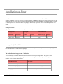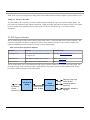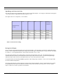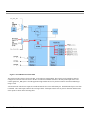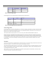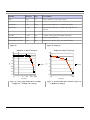
1
X3-A4D4 User's Manual
X3-A4D4 User's Manual
The X3-A4D4 User's Manual was prepared by the technical staff of
Innovative Integration on March 19, 2009.
For further assistance contact:
Innovative Integration
2390-A Ward Ave
Simi Valley, California 93065
PH:
FAX:
(805) 578-4260
(805) 578-4225
email: [email protected]
Website: www.innovative-dsp.com
This document is copyright 2009 by Innovative Integration. All rights
are reserved.
VSS \ Distributions \ A4D4 \ Documentation \ Manual \
A4D4Master.odm
#XXXXXX
Rev 1.0
Table of Contents
X3-A4D4 User's Manual...........................................................................................................................2
Introduction................................................................................................................................................9
Real Time Solutions!...............................................................................................................................................................9
Vocabulary...............................................................................................................................................................................9
What is X3-A4D4? ......................................................................................................................................................9
What is Malibu? ........................................................................................................................................................10
What is C++ Builder?.................................................................................................................................................10
What is Microsoft MSVC?.........................................................................................................................................10
What kinds of applications are possible with Innovative Integration hardware?.......................................................10
Why do I need to use Malibu with my Baseboard?....................................................................................................10
Finding detailed information on Malibu.....................................................................................................................11
Online Help......................................................................................................................................................................11
Innovative Integration Technical Support........................................................................................................................11
Innovative Integration Web Site......................................................................................................................................11
Typographic Conventions......................................................................................................................................................12
Windows Installation...............................................................................................................................13
Host Hardware Requirements................................................................................................................................................13
Software Installation..............................................................................................................................................................13
Tools Registration..................................................................................................................................................................16
Bus Master Memory Reservation Applet...................................................................................................................16
Hardware Installation.............................................................................................................................................................17
After Power-up......................................................................................................................................................................17
Installation on Linux...............................................................................................................................19
Package File Names...................................................................................................................................................19
Prerequisites for Installation..................................................................................................................................................19
The Redistribution Package Group - MalibuRed.............................................................................................................19
Malibu..............................................................................................................................................................................20
Other Software.................................................................................................................................................................20
Baseboard Package Installation Procedure............................................................................................................................20
Board Packages................................................................................................................................................................21
Unpacking the Package....................................................................................................................................................21
Creating Symbolic Links............................................................................................................................................21
Completing the Board Install...........................................................................................................................................22
Linux Directory Structure......................................................................................................................................................22
Applets........................................................................................................................................................................22
Documentation...........................................................................................................................................................22
Examples....................................................................................................................................................................22
Hardware....................................................................................................................................................................22
About the X3 XMC Modules..................................................................................................................23
X3 XMC Architecture...........................................................................................................................................................23
X3 Computing Core...............................................................................................................................................................25
X3 PCI Express Interface......................................................................................................................................................27
Data Buffering and Memory Use...........................................................................................................................................28
X3-A4D4 User's Manual
3
Computational SRAM................................................................................................................................................28
Data Buffer SRAM.....................................................................................................................................................29
EEPROM....................................................................................................................................................................29
Digital I/O..............................................................................................................................................................................29
Software Support..............................................................................................................................................................29
Hardware Implementation................................................................................................................................................30
Digital I/O Timing............................................................................................................................................................31
Digital IO Electrical Characteristics................................................................................................................................31
Notes on Digital IO Use...................................................................................................................................................32
Serial EEPROM Interface......................................................................................................................................................33
Thermal Protection and Monitoring......................................................................................................................................34
Thermal Failures....................................................................................................................................................................35
LED Indicators.......................................................................................................................................................................36
JTAG Scan Path.....................................................................................................................................................................37
FrameWork Logic..................................................................................................................................................................37
Integrating with Host Cards and Systems..............................................................................................................................38
Writing Custom Acquisition Applications............................................................................................40
Snap Example........................................................................................................................................................................40
Tools Required.................................................................................................................................................................40
Program Design................................................................................................................................................................41
The Host Application ............................................................................................................................................................41
User Interface...................................................................................................................................................................41
Setup Tab....................................................................................................................................................................42
Data Streaming...........................................................................................................................................................44
Ram Test.....................................................................................................................................................................45
EEPROM Access........................................................................................................................................................45
Debugging..................................................................................................................................................................45
Host Side Program Organization.....................................................................................................................................45
ApplicationIo....................................................................................................................................................................46
Initialization................................................................................................................................................................46
Logic Loading............................................................................................................................................................49
Starting Data flow.......................................................................................................................................................50
Handle Data Available...............................................................................................................................................54
EEProm Access..........................................................................................................................................................55
Writing Custom Playback Applications................................................................................................57
Wave Example.......................................................................................................................................................................57
Tools Required.................................................................................................................................................................57
Program Design................................................................................................................................................................58
The Host Application ............................................................................................................................................................58
User Interface...................................................................................................................................................................58
Setup Tab....................................................................................................................................................................59
Data Streaming...........................................................................................................................................................62
EEPROM Access........................................................................................................................................................62
Debugging..................................................................................................................................................................63
Host Side Program Organization.....................................................................................................................................63
ApplicationIo....................................................................................................................................................................63
Initialization................................................................................................................................................................63
Logic Loading............................................................................................................................................................66
Handle Data Required................................................................................................................................................71
X3-A4D4 User's Manual
4
EEProm Access..........................................................................................................................................................72
Developing Host Applications.................................................................................................................74
Borland Turbo C++................................................................................................................................................................74
Microsoft Visual Studio 2005................................................................................................................................................76
DialogBlocks.........................................................................................................................................................................78
X3-A4D4 Hardware.................................................................................................................................79
Introduction......................................................................................................................................................................79
A/D Conversion Features.......................................................................................................................................................80
A/D Converters................................................................................................................................................................80
Input Range and Conversion Codes.................................................................................................................................82
Driving the A/D Inputs.....................................................................................................................................................82
A/D Filter Characteristics................................................................................................................................................83
Overrange Detection........................................................................................................................................................83
A/D Sampling Rates.........................................................................................................................................................83
D/A Conversion Features.......................................................................................................................................................83
D/A Converters................................................................................................................................................................83
Output Range and Conversion Codes..............................................................................................................................85
DAC Outputs....................................................................................................................................................................85
DAC Sample Underrun ...................................................................................................................................................86
DAC Update Rates...........................................................................................................................................................86
Sample Rate Generation and Clocking Controls ..................................................................................................................86
External Clock and Reference Inputs...............................................................................................................................89
Generating a Sample Clock with the PLL........................................................................................................................91
PLL Lock and Status........................................................................................................................................................93
PLL Control Interface......................................................................................................................................................94
Notes About Programming the PLL................................................................................................................................95
Timing Analysis...............................................................................................................................................................96
Triggering .............................................................................................................................................................................96
Trigger Source..................................................................................................................................................................97
Framed Trigger Mode......................................................................................................................................................98
Decimation.......................................................................................................................................................................98
FrameWork Logic Functionality...........................................................................................................................................99
Implementing Servo Controls..............................................................................................................................................100
Power Controls and Thermal Design...................................................................................................................................101
System Thermal Design.................................................................................................................................................101
Temperature Sensor and Over Temperature Protection................................................................................................102
Reducing Power Consumption.......................................................................................................................................102
Alert Log..............................................................................................................................................................................103
Overview........................................................................................................................................................................103
Types of Alerts...............................................................................................................................................................103
Alert Packet Format.......................................................................................................................................................104
Software Support............................................................................................................................................................105
Tagging the Data Stream................................................................................................................................................105
Using the X3-A4D4.............................................................................................................................................................105
Where to start?...............................................................................................................................................................105
Getting Good Analog Performance................................................................................................................................106
Application Logic...........................................................................................................................................................106
Calibration...........................................................................................................................................................................107
Production Calibration...................................................................................................................................................107
X3-A4D4 User's Manual
5
Updating the Calibration Coefficients...........................................................................................................................107
Performance Data................................................................................................................................................................108
Power Consumption.......................................................................................................................................................108
Environmental................................................................................................................................................................109
Analog Input...................................................................................................................................................................109
Analog Output................................................................................................................................................................113
Connectors...........................................................................................................................................................................118
Input Connector JP1.......................................................................................................................................................118
XMC P15 Connector......................................................................................................................................................120
XMC P16 Connector......................................................................................................................................................123
Note: PXI Express signals are only available when PXIE adapter card is used............................................................126
Xilinx JTAG Connector.................................................................................................................................................127
Mechanicals.........................................................................................................................................................................128
Applets for the X3 Modules.................................................................................................................................................130
EEProm..........................................................................................................................................................................130
.......................................................................................................................................................................................130
Finder.............................................................................................................................................................................131
Logic Loader ...............................................................................................................................................................132
Applets....................................................................................................................................................133
Common Applets.................................................................................................................................................................133
Registration Utility (NewUser.exe)...............................................................................................................................133
Reserve Memory Applet (ReserveMemDsp.exe).........................................................................................................134
.............................................................................................................................................................................................134
Data Analysis Applets.........................................................................................................................................................134
Binary File Viewer Utility (BinView.exe).....................................................................................................................134
X3-A4D4 User's Manual
6
List of Tables
Table 1. X3 XMC Family......................................................................................................................................................24
Table 2. X3 XMC Family Peripherals...................................................................................................................................24
Table 3. X3 Computing Core Devices...................................................................................................................................25
Table 4. PCI Express Standards Compliance........................................................................................................................27
Table 5. Interfaces from PCI Express to Application Logic..................................................................................................28
Table 6. IUsesExtendedDioPort Class Operations................................................................................................................30
Table 7. Digital I/O Port Timing Parameters.........................................................................................................................31
Table 8. Digital IO Bits Electrical Characteristics................................................................................................................32
Table 9. Digital IOClock Input Electrical Characteristics.....................................................................................................32
Table 10. Temperature Alarms..............................................................................................................................................34
Table 11. X3-SDF FPGA JTAG Scan Path...........................................................................................................................37
Table 12. Development Tools. ..............................................................................................................................................40
Table 13. Development Tools................................................................................................................................................57
Table 14. X3-A4D4 A/D Features.........................................................................................................................................81
Table 15. A/D Conversion Coding........................................................................................................................................82
Table 16. X3-A4D4 DAC Features......................................................................................................................................84
Table 17. DAC Conversion Coding.......................................................................................................................................85
Table 18. Sample Clock Modes.............................................................................................................................................87
Table 19. X3-A4D4 External and Reference Clock Selection..............................................................................................89
Table 20. X3 External Clock and Reference Input Requirements.........................................................................................91
Table 21. External Clock and Reference Signal Pinouts.......................................................................................................91
Table 22. PLL Interface Word Format..................................................................................................................................94
Table 23. PLL Read Sequence...............................................................................................................................................94
Table 24. PLL Read Word.....................................................................................................................................................95
Table 25. PLL Output Assignments......................................................................................................................................95
Table 26. X3-A4D4 External Sample Clock Timing............................................................................................................96
Table 27. External Trigger Inputs..........................................................................................................................................98
Table 28. External Trigger Electrical Characteristics...........................................................................................................98
Table 29. X3-A4D4 Timing for Servo Design....................................................................................................................101
Table 30. Reduced Power Options......................................................................................................................................103
Table 31. Alert Types..........................................................................................................................................................104
Table 32. Alert Packet Format.............................................................................................................................................105
Table 33. X3-A4D4 Power Consumption............................................................................................................................108
Table 34. X3-A4D4 Environmental Limits.........................................................................................................................109
Table 35. X3-A4D4 Analog Input Performance Summary.................................................................................................109
Table 36. X3-A4D4 Analog Output Performance Summary..............................................................................................114
Table 37. X3 XMC Connector P15 Pinout..........................................................................................................................121
Table 38. P15 Signal Descriptions.......................................................................................................................................122
Table 39. X3 XMC Secondary Connector P16 Pinout........................................................................................................124
Table 40. P16 Signal Descriptions.......................................................................................................................................125
Table 41. X3 JP3 Xilinx JTAG Connector Pinout...............................................................................................................128
X3-A4D4 User's Manual
7
List of Figures
Figure 1. X3 XMC Family Block Diagram...........................................................................................................................23
Figure 2. X3 Computing Core Block Diagram......................................................................................................................26
Figure 3. DIO Control Register (BAR1+0x14).....................................................................................................................30
Figure 4. Digital IO Port Addresses.......................................................................................................................................31
Figure 5. Digital I/O Port Timing..........................................................................................................................................31
Figure 6. X3-A4D4 Module (with analog shield removed)...................................................................................................79
Figure 7. X3-A4D4 Block Diagram......................................................................................................................................80
Figure 8. X3-A4D4 A/D Channel Diagram...........................................................................................................................81
Figure 9. X3-A4D4 DAC Channel Diagram.........................................................................................................................85
Figure 10. X3-A4D4 Clock Generation and Controls Block Diagram..................................................................................88
Figure 11. X3-A4D4 External Clock Path.............................................................................................................................90
Figure 12. PLL Reference Prescaling....................................................................................................................................92
Figure 1: Sample Rate Generation Using PLL with post-divider and Tuning Error............................................................93
Figure 13. Sample Triggering ...............................................................................................................................................97
Figure 14. X3-A4D4 FrameWork Logic Data Flow..............................................................................................................99
Figure 15. Servo Loop Timing for X3-A4D4......................................................................................................................100
Figure 17. Analog Input Bandwidth 0 to 10 MHz (sample rate = 4 MSPS, Vin= 10Vp-p)...............................................110
Figure 18. Analog In............................................................................................................................................................110
Figure 19. put Bandwidth 100 to 100 kHz (sample rate = 4 MSPS, Vin= 10Vp-p)...........................................................110
Figure 20. Signal quality measurement (1.01 kHz input, 5Vp-p, sample rate = 1 MSPS, 256K FFT)...............................111
Figure 21. Signal Quality vs Input Amplitude (sample rate = 4 MSPS, 1.01 kHz sine).....................................................112
Figure 22. Signal Quality vs Sample Rate (Vin = 5Vp-p, 1.01 kHz sine)..........................................................................112
Figure 23. Noise floor (grounded input, Fs= 3.888 MSPS).................................................................................................113
Figure 24. Noise (grounded input, Fs= 3.888 MSPS).........................................................................................................113
Figure 25. Step response for 7V input see next figure(Fs = 3.888 MSPS)..........................................................................113
Figure 26. Step Input , 7Vp-p used for step input response.................................................................................................113
Figure 27. Output Spectral Measurement, Update rate = 10 MSPS, 10Vp-p, 1.2kHz........................................................115
Figure 28. Output Signal Quality vs Update Rate...............................................................................................................116
Figure 29. Output Spurious Signal Quality vs Frequency...................................................................................................116
Figure 30. Output Settling for 20V Step..............................................................................................................................117
Figure 31. P15 XMC Connector Orientation.......................................................................................................................120
Figure 32. P16 XMC Connector Orientation.......................................................................................................................123
Figure 33. X3-A4D4 J3 Orientation....................................................................................................................................127
Figure 34. X3-A4D4 J3 Side View......................................................................................................................................127
Figure 35. X3-A4D4 Mechanicals (Bottom View) Rev B..................................................................................................129
Figure 36. X3-A4D4 Mechanicals (Top View) Rev B........................................................................................................129
X3-A4D4 User's Manual
8
Introduction
Real Time Solutions!
Thank you for choosing Innovative Integration, we appreciate your business! Since 1988, Innovative Integration has grown
to become one of the world's leading suppliers of DSP and data acquisition solutions. Innovative offers a product portfolio
unrivaled in its depth and its range of performance and I/O capabilities .
Whether you are seeking a simple DSP development platform or a complex, multiprocessor, multichannel data acquisition
system, Innovative Integration has the solution. To enhance your productivity, our hardware products are supported by
comprehensive software libraries and device drivers providing optimal performance and maximum portability.
Innovative Integration's products employ the latest digital signal processor technology thereby providing you the competitive
edge so critical in today's global markets. Using our powerful data acquisition and DSP products allows you to incorporate
leading-edge technology into your system without the risk normally associated with advanced product development. Your
efforts are channeled into the area you know best ... your application.
Vocabulary
X3-A4D4 User's Manual
9
What is X3-A4D4?
The X3 module Family are XMC (VITA 42.3) modules with a variety of IO capabilities and a PCI Express interface. Each
modules has a Spartan 3 application FPGA, buffer memory and clocking features to support the IO functions. Two SRAMs
are used, one each for buffer memory and application memory. Then XMC has a 32/66 PCI interface to a single lane PCIe
bridge chip DIO using P16 connection to the baseboard.
For sample rate generation, the X3-A4D4 has a precision, low noise PLL or external clocks. Trigger modes including
software, framed and external triggering provide precise control over sample acquisition and synchronization with other
devices. Timestamped alerts also provide the ability to monitor the acquisition process and correlate system events to the
data.
Data acquisition control, signal processing, buffering, and system interface functions are implemented in a Xilinx Spartan3A
DSP FPGA, 1.8 M gate device. Two 1Mx16 memory devices are used for data buffering and FPGA computing memory.
The logic can be fully customized using VHDL and MATLAB using the FrameWork Logic toolset. The MATLAB BSP
supports real-time hardware-in-the-loop development using the graphical, block diagram Simulink environment with Xilinx
System Generator.
The PCI Express interface supports continuous data rates up to 180 MB/ s between the module and the host. A flexible data
packet system implemented over the PCIe interface provides both high data rates to the host that is readily expandable for
custom applications.
What is Malibu?
Malibu is the Innovative Integration-authored component suite, which combines with the Borland, Microsoft or GNU C++
compilers and IDEs to support programming of Innovative hardware products under Windows and Linux. Malibu supports
both high-speed data streaming plus asynchronous mailbox communications between the DSP and the Host PC, plus a wealth
of Host functions to visualize and post-process data received from or to be sent to the target DSP.
What is C++ Builder?
C++ Builder is a general-purpose code-authoring environment suitable for development of Windows applications of any type.
Armada extends the Builder IDE through the addition of functional blocks (VCL components) specifically tailored to
perform real-time data streaming functions.
What is Microsoft MSVC?
MSVC is a general-purpose code-authoring environment suitable for development of Windows applications of any type.
Armada extends the MSVC IDE through the addition of dynamically created MSVC-compatible C++ classes specifically
tailored to perform real-time data streaming functions.
X3-A4D4 User's Manual
10
What kinds of applications are possible with Innovative Integration hardware?
Data acquisition, data logging, stimulus-response and signal processing jobs are easily solved with Innovative Integration
baseboards using the Malibu software. There are a wide selection of peripheral devices available in the Matador DSP
product family, for all types of signals from DC to RF frequency applications, video or audio processing. Additionally,
multiple Innovative Integration baseboards can be used for a large channel or mixed requirement systems and data
acquisition cards from Innovative can be integrated with Innovative's other DSP or data acquisition baseboards for highperformance signal processing.
Why do I need to use Malibu with my Baseboard?
One of the biggest issues in using the personal computer for data collection, control, and communications applications is the
relatively poor real-time performance associated with the system. Despite the high computational power of the PC, it cannot
reliably respond to real-time events at rates much faster than a few hundred hertz. The PC is really best at processing data,
not collecting it. In fact, most modern operating systems like Windows are simply not focused on real-time performance, but
rather on ease of use and convenience. Word processing and spreadsheets are simply not high-performance real-time tasks.
The solution to this problem is to provide specialized hardware assistance responsible solely for real- time tasks. Much the
same as a dedicated video subsystem is required for adequate display performance, dedicated hardware for real-time data
collection and signal processing is needed. This is precisely the focus of our baseboards – a high performance, state-of-theart, dedicated digital signal processor coupled with real-time data I/O capable of flowing data via a 64-bit PCI bus interface.
The hardware is really only half the story. The other half is the Malibu software tool set which uses state of the art software
techniques to bring our baseboards to life in the Windows environment. These software tools allow you to create applications
for your baseboard that encompass the whole job - from high speed data acquisition, to the user interface.
Finding detailed information on Malibu
Information on Malibu is available in a variety of forms:
•
Data Sheet (http://www.innovative-dsp.com/products/malibu.htm)
•
On-line Help
•
Innovative Integration Technical Support
•
Innovative Integration Web Site (www.innovative-dsp.com)
Online Help
Help for Malibu is provided in a single file, Malibu.chm which is installed in the Innovative\Documentation folder during the
default installation. It provides detailed information about the components contained in Malibu - their Properties, Methods,
Events, and usage examples. An equivalent version of this help file in HTML help format is also available online at
http://www.innovative-dsp.com/support/onlinehelp/Malibu.
Innovative Integration Technical Support
Innovative includes a variety of technical support facilities as part of the Malibu toolset. Telephone hotline supported is
available via
X3-A4D4 User's Manual
11
Hotline (805) 578-4260 8:00AM-5:00 PM PST.
Alternately, you may e-mail your technical questions at any time to:
[email protected].
Also, feel free to register and browse our product forums at http://forum.iidsp.com/, which are an excellent source of FAQs
and information submitted by Innovative employees and customers.
Innovative Integration Web Site
Additional information on Innovative Integration hardware and the Malibu Toolset is available via the Innovative Integration
website at www.innovative-dsp.com
Typographic Conventions
This manual uses the typefaces described below to indicate special text.
Typeface
Source Listing
Boldface
Emphasis
Cpp Variable
Cpp Symbol
KEYCAPS
Menu Command
X3-A4D4 User's Manual
Meaning
Text in this style represents text as it appears onscreen or in code. It
also represents anything you must type.
Text in this style is used to strongly emphasize certain words.
Text in this style is used to emphasize certain words, such as new
terms.
Text in this style represents C++ variables
Text in this style represents C++ identifiers, such as class, function,
or type names.
Text in this style indicates a key on your keyboard. For example,
“Press ESC to exit a menu”.
Text in this style represents menu commands. For example “Click
View | Tools | Customize”
12
Windows Installation
This chapter describes the software and hardware installation procedure for the Windows platform (WindowsXP and Vista).
Do NOT install the hardware card into your system at this time. This will follow the software
installation.
Host Hardware Requirements
The software development tools require an IBM or 100% compatible Pentium IV - class or higher machine for proper
operation. An Intel-brand processor CPU is strongly recommended, since AMD and other “clone” processors are not
guaranteed to be compatible with the Intel MMX and SIMD instruction-set extensions which the Armada and Malibu Host
libraries utilize extensively to improve processing performance within a number of its components. The host system must
have at least 128 Mbytes of memory (256MB recommended), 100 Mbytes available hard disk space, and a DVD-ROM
drive. Windows2000 or WindowsXP (referred to herein simply as Windows) is required to run the developer’s package
software, and are the target operating systems for which host software development is supported.
Software Installation
The development package installation program will guide you through the installation process.
Note: Before installing the host development libraries (VCL components or MFC classes), you must
have Microsoft MSVC Studio (version 9 or later) and/or Codegear RAD Studio C++ (version 11)
installed on your system, depending on which of these IDEs you plan to use for Host development. If
you are planning on using these environments, it is imperative that they are tested and knownoperational before proceeding with the library installation. If these items are not installed prior to
running the Innovative Integration install, the installation program will not permit installation of the
associated development libraries. However, drivers and DLLs may be installed to facilitate field
deployment.
You must have Administrator Privileges to install and run the software/hardware onto your system, refer to the Windows
documentation for details on how to get these privileges.
X3-A4D4 User's Manual
13
Starting the Installation
To begin the installation, start Windows. Shut down all running programs and disable anti-virus software. Insert the
installation DVD. If Autostart is enabled on your system, the install program will launch. If the DVD does not Autostart,
click on Start | Run... Enter the path to the Setup.bat program located at the root of your DVD-ROM drive (i.e.
E:\Setup.bat) and click “OK” to launch the setup program.
SETUP.BAT detects if the OS is 64-bit or 32-bit and runs the appropriate installation for each
environment. It is important that this script be run to launch an install.
When installing on a Vista OS, the dialog below may pop up. In each case, select “Install this driver software anyway” to
continue.
Figure 1. Vista Verificaton Dialog
X3-A4D4 User's Manual
14
The Installer Program
After launching Setup, you will be presented with the following screen.
Figure 2. Innovative Install Program
Using this interface, specify which product to install, and where on your system to install it.
1) Select the appropriate product from the Product Menu.
2) Specify the path where the development package files are to be installed. You may type a path or click “Change” to
browse for, or create, a directory. If left unchanged, the install will use the default location of “C:\Innovative”.
3) Typically, most users will perform a “Full Install” by leaving all items in the “Components to Install” box
checked. If you do not wish to install a particular item, simply uncheck it. The Installer will alert you and
automatically uncheck any item that requires a development environment that is not detected on your system.
4) Click the Install button to begin the installation.
Note: The default “Product Filter” setting for the installer interface is “Current Only” as indicated by
the combo box located at the top right of the screen. If the install that you require does not appear in the
“Product Selection Box” (1), Change the “Product Filter” to “Current plus Legacy”.
X3-A4D4 User's Manual
15
Each item of the checklist in the screen shown above, has a sub-install associated with it and will open a sub-install screen if
checked. For example, the first sub-install for “Quadia - Applets, Examples, Docs, and Pismo libraries” is shown below.
The installation will display a progress window, similar to the one shown below, for each item checked.
Figure 1. Progress is shown for each section.
X3-A4D4 User's Manual
16
Tools Registration
At the end of the installation process you will be prompted to register.
If you decide that you would like to register at a later time, click
“Register Later”.
When you are ready to register, click Start | All Programs | Innovative |
<Board Name> | Applets. Open the New User folder and launch
NewUser.exe to start the registration application. The registration
form to the left will be displayed.
Before beginning DSP and Host software development, you must
register your installation with Innovative Integration. Technical
support will not be provided until registration is successfully
completed. Additionally, some development applets will not operate
until unlocked with a passcode provided during the registration
process.
It is recommend that you completely fill out this form and return it to
Innovative Integration, via email or fax. Upon receipt, Innovative
Integration will provide access codes to enable technical support and
unrestricted access to applets.
Figure 2. ToolSet registration form
Bus Master Memory Reservation Applet.
At the conclusion of the installation process, ReserveMem.exe will run
(except for SBC products). This will allow you to set the memory size
needed for the busmastering to occur properly. This applet may be run from
the start menu later if you need to change the parameters.
For optimum performance each Matador Family Baseboard requires 2 MB
of memory to be reserved for its use. To reserve this memory, the registry
must be updated using the ReserveMem applet. Simply select the Number
of Baseboards you have on your system, click Update and the applet will
update the registry for you. If at any time you change the number of boards
in your system, then you must invoke this applet found in Start | All
Programs | Innovative | <target board> | Applets | Reserve Memory.
After updating the system exit the applet by clicking the exit button to
resume the installation process.
Figure 3. BusMaster configuration
X3-A4D4 User's Manual
17
At the end of the install process, the following screen will appear.
Figure 4. Installation complete
Click the “Shutdown Now” button to shut down your computer. Once the shutdown process is complete unplug the system
power cord from the power outlet and proceed to the next section, “Hardware Installation.”
Hardware Installation
Now that the software components of the Development Package have been installed the next step is to configure and install
your hardware. Detailed instructions on board installation are given in the Hardware Installation chapter, following this
chapter.
IMPORTANT: Many of our high speed cards, especially the PMC and XMC Families, require forced
air from a fan on the board for cooling. Operating the board without proper airflow may lead to
improper functioning, poor results, and even permanent physical damage to the board. These boards
also have temperature monitoring features to check the operating temperature. The board may also be
designed to intentionally fail on over-temperature to avoid permanent damage. See the specific
hardware information for airflow requirements.
X3-A4D4 User's Manual
18
After Power-up
After completing the installation, boot your system into Windows.
Innovative Integration boards are plug and play compliant, allowing Windows to detect them and auto-configure at start-up.
Under rare circumstances, Windows will fail to auto-install the device-drivers for the JTAG and baseboards. If this happens,
please refer to the “TroubleShooting” section.
X3-A4D4 User's Manual
19
Installation on Linux
This chapter contains instruction on the installation of the baseboard software for Linux operating systems.
Software installation on Linux is performed by loading a number of packages. A Package is a special kind of archive file that
contains not only the files that are to be installed, but also installation scripts and dependency information to allow a smooth
fit into the system. This information allows the package to be removed, or patched. Innovative uses RPM packages in its
installs.
Package File Names
A package file name such as Malibu-LinuxPeriphLib-1.1-3.i586.rpm encodes a lot of information.
Package Name
Distribution
Malibu-Linux
Package ID
Subpackage
PeriphLib
Version
1.1
Information Fields
Revision
Hardware Type
Extension
3
i586
.rpm
Prerequisites for Installation
In order to properly use the baseboard example programs and to develop software using the baseboard, some packages need
to be installed before the actual baseboard package.
The Redistribution Package Group - MalibuRed
This set of packages contain the libraries and drivers needed to run a program using Malibu. This group is called
“MalibuRed” because it contains the packages needed to allow running Malibu based programs on a target, non-development
machine. (Red is short for 'redistributable').
MalibuRed Packages
Description
WinDriver-9.2-1.i586.rpm
Installs WinDriver 9.2 release.
MalibuLinux-Red-[ver]-[rel].i586.rpm
Installs Baseboard Driver Kernel Plugin.
intel-ipp_rti-5.3p.x32.rpm
Installs Intel IPP library redistributable files.
X3-A4D4 User's Manual
20
The installation CD, or the web site contains a file called LinuxNotes.pdf giving instructions on how to load these packages
and how to install the drivers onto your Linux machine. This file is also loaded onto the target machine by the the MalibuLinuxRed RPM. These procedures need to be completed for every target machine.
Malibu
To develop software for a baseboard the Malibu packages also must be installed.
Malibu Packages
Description
Malibu-LinuxPeriphLib-[ver]-[rel].i586.rpm
Installs Malibu Source, Libraries and Examples.
Other Software
Our examples use the DialogBlocks designer software and wxWidgets GUI library package for user interface code. If you
wish to rebuild the example programs you will have to install this software as well.
Package
wxWidgets
DialogBlocks
Company
URL
wxWidgets
http://www.wxwidgets.org
Anthemion
http://www.anthemion.co.uk.org/dialogblocks
Baseboard Package Installation Procedure
Each baseboard installation for Linux consists of one or more package files containing self-extracting packages of
compressed files, as listed in the table below. Note that package version codes may vary from those listed in the table.
Each of these packages automatically extract files into the /usr/Innovative folder, herein referred to as the Innovative
root folder in the text that follows. For example, the X5-400 RPM extracts into /usr/Innovative/X5-400-[ver]. A
symbolic link named X5-400 is then created pointing to the version directory to allow a single name to apply to any version
that is in use.
X3-A4D4 User's Manual
21
Board Packages
Baseboard
Packages
Description
X5-400M
Malibu-LinuxPeriphLib-[ver]-[rel].i586.rpm
Board files and examples.
X5-210M
X5-210M-LinuxPeriphLib-[ver]-[rel].i586.rpm
Board files and examples.
X3-10M
X3-10M-LinuxPeriphLib-[ver]-[rel].i586.rpm
Board files and examples.
X3-25M
X3-25M-LinuxPeriphLib-[ver]-[rel].i586.rpm
Board files and examples.
X3-A4D4
X3-A4D4-LinuxPeriphLib-[ver]-[rel].i586.rpm
Board files and examples.
X3-SD
X3-SD-LinuxPeriphLib-[ver]-[rel].i586.rpm
Board files and examples.
X3-SDF
X3-SDF-LinuxPeriphLib-[ver]-[rel].i586.rpm
Board files and examples.
X3-Servo
X3-Servo-LinuxPeriphLib-[ver]-[rel].i586.rpm
Board files and examples.
SBC-ComEx
Sbc-ComEx-LinuxPeriphLib-[ver]-[rel].i586.rpm
Board files and examples.
Unpacking the Package
As root, type:
rpm -i -h X5-400-LinuxPeriphLib-1.1-4.i586.rpm
This extracts the X5-400 board files into the Innovative root directory. Use the package for the particular board you are
installing.
Creating Symbolic Links
The example programs assume that the user has created symbolic links for the installed board packages. A script file is
provided to simplify this operation by the Malibu Red package. In the MalibuRed/KerPlug directory, there is a script called
quicklink.
quicklink X5-400 1.1
These commands will create a symbolic link X5-400 pointing to X5-400-1.1.
This script can be moved to the user's bin directory to allow it to be run from any directory.
X3-A4D4 User's Manual
22
Completing the Board Install
The normal board install is complete with the installation of the files. The board driver install is already complete with the
loading of the Malibu Red package. If there are any board-specific steps they will be listed at the end of this chapter.
Linux Directory Structure
When a board package is installed, its files are placed under the /usr/Innovative folder. The base directory is named
after the board with a version number attached -- for example, the version 2.0 X5-400 RPM extracts into
/usr/Innovative/X5-400-2.0.
This allows multiple version of installs to coexist by using a symbolic link to point to a particular version. Changing the
symbolic link changes with version will be used.
Under the main directory there are a number of subdirectories.
Applets
The applets subdirectory contains small application programs that aid in the use of the board. For example, there is a Finder
program that allows the user to flash an LED on the board to determine which board is associated with a target number. See
the Applets chapter for a fuller description of the applets for a board.
Documentation
This directory contains any documentation files for the project. Open the index.html file in the directory with a web browser
to see the available files and a description of the contents.
Examples
This directory and its subdirectories contain the projects, source and example programs for the board.
Hardware
This directory contains files associated with programming the board Logic and any logic images provided.
X3-A4D4 User's Manual
23
About the X3 XMC Modules
In this chapter, we will discuss the common features of the X3 module family. Specifics on each module are covered in later
chapters.
X3 XMC Architecture
The X3 XMC modules share a common architecture as well as many features such as the PCI Express interface, data
buffering features, the Application Logic, and other system integration features. This allows the X3 XMC modules to utilize
common software and logic firmware, while providing unique analog and digital features.
Figure 5. X3 XMC Family Block Diagram
The X3 XMCs have a variety of analog and digital IO front ends suited to many applications.
X3-A4D4 User's Manual
24
Table 1. X3 XMC Family
X3 XMC
Features
FPGA
Applications
X3-SD
16 channels of 24-bit, 216 ksps A/D, >100
dB
Xilinx Spartan3 1M
(2M option)
Vibration measurement,
acoustics, wide dynamic
range applications
X3-SDF
4 channels of variable resolution/speed A/
D up to 24-bit, 5 MSPS or 16-bit 20 MSPS,
>100 dB below 2.5 MSPS
Xilinx Spartan3 1M
(2M option)
Vibration measurement,
acoustics, wide dynamic
range applications
X3-25M
Two channels of 25 MSPS, 16-bit A/D and
two channels of 16-bit, 50 MSPS DAC, 16bits front panel DIO
Xilinx Spartan3A DSP 1.8M
Ultrasound, pulse digitizing,
waveform generation and
stimulus-response
X3-A4D4
4 channels of 16-bit, 4 MSPS A/D and 4
channels 16-bit 2 MHz DAC with low
latency, 8-bits front panel DIO
Xilinx Spartan3A DSP 1.8M
Servo controls, process
instrumentation
X3-Servo
12 channels 16-bit, 250 ksps A/D and 12
channels 16-bit 250 ksps DAC, low
latency, 16-bits front panel DIO
Xilinx Spartan3A DSP 1.8M
(3.4M option)
Electromechanical controls,
process instrumentation
X3-DIO
64 bits/32 pairs digital IO to FPGA,
LVCMOS or LVDS, with streaming,
playback and capture features
Xilinx Spartan3A DSP 1.8M
(3.4M option)
Test pattern generation,
remote IO interfaces, digital
controls
X3-10M
8 channels of 16-bit, 25 MSPS A/D with
programmable gain and instrumentation
front end; Xilinx Spartan3A DSP FPGA
Xilinx Spartan3A DSP 1.8M
Measurement for high speed
vibration, ultrasound fault
detection systems,
neurophysical applications
The X3 XMCs feature a Xilinx Spartan3 or Spartan3A DSP FPGA core for signal processing and control. In addition to the
features in the Spartan3/3A logic such as embedded multipliers and memory blocks, the FPGA computing core has two local
SRAMs for data buffering and computing memory.
There are also a number of support peripherals for IO control and system integration. Each XMC may have additional
application-specific support peripherals.
Table 2. X3 XMC Family Peripherals
Peripheral
Features
XMC.3 PCI Express
interface
The XMC.3 host interface Integrates with PCI Express systems using one lane operating at 2.5 Gbps
that provides up to 180 MB/s sustained data rates. This interface complies with VITA standard 42.3
which specifies PCI Express interface for the XMC module format.
The Velocia packet system provides fast and flexible communications with the host using a creditbased flow control supporting packet transfers with the host. A secondary command channel provides
independent interface for control and status outside of the data channel that is extensible to custom
applications.
XMC P16
Provides digital IO or a private link to host cards capable of >200 MB/s sustained operation.
X3-A4D4 User's Manual
25
Peripheral
Features
Timing and triggering
Flexible clocking and synchronization features for IO
Data buffering and
Computational Memory
Two 2MB SRAM devices are used provide data buffering, processor memory and computation
memory for the Application FPGA
Alert Log
Monitors system events and error conditions to help manage the data acqusiton process
Temperature Sensor
Monitors the module temperature and provides thermal protection for the module
X3 Computing Core
The X3 XMC module family has an FPGA-based computing core that controls the data acquisition process, providing data
buffing and host communications. The computing core consists of a Xilinx Spartan3 or 3A DSP FPGA and two banks of
2MB SRAM memory. The FPGA uses the memories for data buffering and computational workspace.
Table 3. X3 Computing Core Devices
Feature
Application Logic
FPGA
X3 Module
Device
Part Number
SD, SDF
Xilinx Spartan 3 1M
XC3S1000-4FGG456C
10M, Servo, 25M, DIO
Xilinx Spartan 3A DSP 1.8M
XC3SD1800-4FGG676C
Buffer Memory
SRAM
SD, SDF
Synchronous Burst ZBT
SRAM
1Mx16, 100 MHz
Computational
Memory SRAM
SD, SDF
Synchronous Burst ZBT
SRAM
1Mx16, 100 MHz
10M, Servo, 25M, DIO
10M, Servo, 25M, DIO
512Kx32, 133 MHz
512Kx32, 133 MHz
The main focus of the module is the X3's computing core which connects the IO, peripherals, host communications and
support features. Each IO device directly connects to the application FPGA on the X3 module, providing tight coupling for
high performance. (Real-time IO). The FPGA logic implements an interface to each device that connects them to the
controls and data communications features on the module. Support features, such as sample triggering and data analysis, are
implemented in the logic to provide precise real-time control over the data acquisition process.
X3-A4D4 User's Manual
26
X3 Computing Core Block Diagram
The X3 module architecture is really defined by the features in the logic that connect the IO devices to the Velocia packet
system. For data from IO devices such as A/Ds, the data flows from the IO interface and is then enqueued in the multi-queue
buffer. The packetizer then creates data packets from the data stream that are moved across the data link to the PCIe
interface. Packets to output devices travel in the opposite direction – from the link to the deframer and into the multi-queue
data buffer. The output IO, such as a DAC, then consumes the data from the queue as required. The Alert Log monitors
error conditions and important events for management of the data acquisition process.
The host interacts with the X3 computing core using the packet system for high speed data and over the command channel.
The packet system is the main data channel to the card and delivers the high performance, real-time data capability of moving
data to and from the module. Since it uses an efficient DMA system, it is very efficient at moving data which leaves the host
system unburdened by the data flow. The command channel provides the PCIe host direct access to the computing core logic
for status, control and initialization. Since it is outside the packet system, it is less complex to use and provides unimpeded
access to the logic.
The application FPGA image is loaded by the host computer as part of the module initialization. The image is loaded over the
SelectMAP interface to the FPGA, which is a byte-wide configuration port on the FPGA, from the host PCI Express
interface. The configuration port for the FPGA is independent of the packet interface to the host and does not involve the use
of the Velocia packet system. The image can be loaded at any time over the SelectMAP interface allowing dynamic
configuration of the FPGA for advanced applications.
X3-A4D4 User's Manual
27
Note: There is no on-card storage for this image and it must be loaded each time the host computer is powered down or reset.
Adding New Features to the FPGA
The functionality of the computing core can be modified using the FrameWork Logic tools for the X3 module family. The
tools support development in either VHDL or MATLAB. Signal processing, data analysis and unique functions can be added
to the X3 modules to suit application-specific requirements. See the X3 FrameWork Logic User Guide for further
information.
X3 PCI Express Interface
The X3 module family has a PCI Express interface that provides a lane, 2.5 Gbps full duplex link to the host computer. The
interface is compatible with industry standard PCI Express systems and may be used in a variety of host computers. The
following standards govern the PCI Express interface on the X3 XMC modules.
Table 4. PCI Express Standards Compliance
Standard
Describes
Standards Group
PCI Express 1.0a
PCI Express electrical and protocol standards.
2.5 Gbps data rate.
PCI SIG ( http://www.picmg.com )
ANSI/VITA 42
XMC module mechanicals and connectors
VITA ( www.vita.org )
ANSI VITA 42.3
XMC module with PCI Express Interface.
VITA ( www.vita.org )
The X3 module family uses a Texas Instruments bridge chip to go from PCI Express to a local PCI bus on the module. The
PCI Express bridge works with the PCI FGPA to implement the Velocia packet system for data communications and also
provides the module configuration and control features.
Data link to App Logic
32-bit, 66 MHz
PCI Express
Bridge
PCI Express
1x lane
Connector P15
X3-A4D4 User's Manual
Local PCI Bus
32-bit, 66 MHz
FPGA
PCI Interface
Command Channel
Serial Link
SelectMAP interface to
app logic
28
The major interfaces to the application logic are the data link, command channel and SelectMAP interface. The data link
provides a high performance channel for the application logic to communicate with the host computer while the Command
Channel is a command and control interface from the host computer to the application logic. The SelectMAP interface is the
application FPGA configuration port for loading the logic image.
The data link is the primary data path for the data communications between the application FPGA and host computer. When
data packets are created by the application logic, such as A/D samples, or required by the application logic for output devices,
such as DAC channels, the data flows over the data link as packets. The maximum transfer rate over the data link is 264 MB/
s, with a 220 MB/s sustained rate. The data packets contain a Peripheral Device Number (PDN) that identifies the peripheral
associated with the this data packet. In this way, the packet system is extensible to other devices that may be added to the
logic. For example, an FFT analysis can be added to the logic and its result sent to the host as a new PDN for display and
further analysis while maintaining other data streams from A/D channels.
Table 5. Interfaces from PCI Express to Application Logic
Application Logic
Interface
Max Data Rate
Typical Use
Data Link
264 MB/s burst, 240 MB/s sustained
Velocia packet system interface main path for data communications
Command Channel
5 MB/s sustained
Command, control and status
SelectMAP
5 MB/s
Application logic configuration
Data Buffering and Memory Use
There are two 2MB SBSRAM devices attached to the application FPGA that provide data buffering and computational RAM
for FPGA applications.
Computational SRAM
The SRAM on the X3 family is a 2MB memory dedicated as FPGA local memory. Applications in the FPGA may use the
SRAM as a local buffer memory if the data buffer is too large to fit in FPGA block RAMs, or as memory for an embedded
processor in the FPGA.
The SRAM device connected to each Application FPGA is 2 MB total size, organized as 1M by 16 bits (X3-SD and X3SDF) or 512K by 32 bits (all others). This device is a synchronous, ZBT SRAM and supports clock rates up to 100 MHz on
X3-SD and X3-SDF, 133 MHz on all other modules. All SRAM control and data lines pins are directly connected to the
FPGA, allowing the SRAM memory control to be customized to the application.
The Framework Logic provides a simple SRAM interface that can be readily modified for many types of applications.
Detailed explanation of the interface control logic is described in the FrameWork Logic User Guide. The Framework Logic
provides a simple register interface to the SBSRAM control logic that is used for test and demonstration. FPGA logic
developers can easily replace the simple register interface logic to build on top of the high performance logic core when
integrating the SRAM into their logic design.
X3-A4D4 User's Manual
29
MATLAB developers frequently use the SRAM as the real-time data buffer during development. Since the MATLAB
Simulink tools operate over the FPGA JTAG during development at a low rate, it is necessary to use the SRAM for real-time,
high speed data buffering. The MATLAB Simulink library for the X3 modules demonstrate the use of the SRAM as a data
capture buffer. The SRAM captures real-time, high-speed data that can then be read out into MATLAB for analysis or
display as a snapshot. This allows high-speed, real-time to be captured and brought into MATLAB Simulink over the slow
(10Mb/sec) JTAG link. See the X3 FrameWork Logic User Guide for more details and examples.
Data Buffer SRAM
The second SRAM is provides a 2MB memory pool local to the FPGA. The Framework Logic implements a data buffer with
one or more queues for the A/D and D/A streams as appropriate for the particular X3 module.
In the Framework logic, the SRAM use is demonstrated as a multiple queue FIFO memory that divides the 2 MB memory
buffer into separate queues (virtual FIFOs) for input and output.. The logic component, referred to as Multi-Queue SRAM,
controls the SRAM to create the FIFO queue functionality. Custom logic applications can use the Multi Queue SRAM buffer
component to add additional queues for new devices.
EEPROM
A serial EEPROM on the X3 modules is used to store configuration and calibration information. The interface to the serial
EEPROM is an I2C bus that is controlled by the PCI logic device. The device is an Atmel AT24C16-10SI, a 16K bit device.
The I2C bus is slow and the calibration is read out of the EEPROM at initialization time by the application software and
written into registers in the application logic for real-time error correction.
The EEPROM also has a write cycle limit of 100K cycles, so it should only be written to when calibration is performed or
configuration information changes. Once the write cycle duration limit is exceeded, the device will not reliably store data
any more.
Digital I/O
The X3 modules have a digital IO port and is accessible over P16 that provides basic bit IO. The port provides 44 bits of IO that
may be used as inputs or outputs and a differential clock input. The port is configured and accesses directly from the PCI
Express host. For more advance applications, digital IO port may be reconfigured in custom logic applications for a variety
purposes since it provides direct connections to the applicant FPGA.
The DIO port is presented on P16. See the connectors section of this chapter the connector pin out and information about the
connector.
Software Support
The digital I/O hardware is controlled by the IUsesExtendedDioPort class. Its properties:
X3-A4D4 User's Manual
30
Table 6. IUsesExtendedDioPort Class Operations
Function
Type
Description
DioPortConfig()
Property
Configures banks of bits for input or output
DioPortData()
Property
DioPortDataHigh()
Property
Broadside Read/Write to low-order 32-bits of
DIO.
Broadside Read/Write to high-order 12-bits of
DIO. Only
Typical use of the digital IO port involves first configuring the port using the Config() operator. This sets the byte direction
and the clock mode. The port is then ready for read/write configurations to each port.
Hardware Implementation
Digital I/O port activity is controlled by the digital I/O configuration control and data register. Port direction is controlled by
the configuration control register.
Bit
Function
0
DIO bits 7..0 direction control, 0=input, default
1
DIO bits 15..8 direction control, 0=input, default
2
DIO bits 23..16 direction control, 0=input, default
3
DIO bits 31..24 direction control, 0=input, default
4
DIO bits 39..32 output enable. '0' = input, default
5
DIO bits 43..40 output enable. '0' = input, default
30..6
-
31
Sample DIO inputs when DIO_EXT_CLK is true, otherwise always
sample
(0=sample always, default)
Figure 1. DIO Control Register (BAR1+0x14)
Port
X3-A4D4 User's Manual
Address
DIO_L
BAR1+0x13
DIO_H
BAR1+0x16
31
Figure 2. Digital IO Port Addresses
Data may be written to/read from the digital I/O port using the digital I/O port data registers. Data written to ports bits which
are set for output mode will be latched and driven to the corresponding port pins, while data written to input bits will be
ignored. The input DIO may be clocked externally by enabling the external digital clock bit in the appropriate configuration
register. If the internal clock is used, the data is latched at the beginning of any read from the port. Data read from output bits
is equal to the last latched bit values (i.e. the last data written to the port by the host ).
Digital I/O port pins are pulled down to digital ground within the logic device. Consequently, the state of the DIO pins do
not change as power is applied to the PC during system start-up. The pulldown resistor is about 8K ohms.
External signals connected to the digital I/O port bits or timer input pins should be limited to a voltage range between 0 and
3.3V referenced to ground on the digital I/O port connector. Exceeding these limits will cause damage to the X3 module.
Digital I/O Timing
The following diagram gives timing information for the digital I/O port when used in external readback clock mode (see
above for details). This data is derived from device specifications and is not factory tested.
Figure 3. Digital I/O Port Timing
Table 1. Digital I/O Port Timing Parameters
Parameter
min. (ns)
tSU
tH
5
0
Digital IO Electrical Characteristics
The digital IO pins are LVTTL compatible pins driven by 3.3V logic. The DIO port connects directly to the application
FPGA. The DIO input clock is LVDS, a differential input.
Warning: the DIO pins are NOT 5V compatible. Input voltage must not exceed 3.6V.
X3-A4D4 User's Manual
32
Parameter
Value
Notes
Input Voltage
Max = 3.6V
Min = -0.3V
Exceeding these will damage
the application FPGA
Output Voltage
''1' > 3.0V
'0' < 0.8V
For load < +/-12mA
Output Current
+/-12mA
FPGA can be reconfigured for
custom designs for other drive
currents.
Input Logic
Thresholds
'1' >= 2VDC
'0' < 0.8VDC
Input Impedance
>1M ohm || 15 pF
Excludes cabling
Pulldown
8K ohms
Pulldown is in the logic.
Table 2. Digital IO Bits Electrical Characteristics
Parameter
Value
Notes
Input Voltage
Max = 3.6V
Min = -0.3V
Exceeding these will damage
the application FPGA
Signaling
Standard
LVDS 2.5V
EIA-644
Input common
mode voltage
Min =0.30V
Typ = 1.25V
Max =2.20V
Input Logic
Thresholds
Min = 0.10V
Typ = 0.30V
Max = 0.60V
Termination
100 ohms
Differential voltage Vin+ - Vin-
Table 3. Digital IO Clock Input Electrical Characteristics
Notes on Digital IO Use
The digital IO on X3 family, as supported using the standard FrameWork Logic, is intended for low speed bit IO controls and
status. The interface is capable of data rates exceeding 75MHz and custom logic developers can implement much higher
speed and sophisticated interfaces by modifying the logic. The digital IO clock input, and LVDS signal pair, is a capable of
rates exceeding 200 MHz.
Since the bit IO is connected to the command channel interface in the standard logic, this limits the effective update or read
rate to about 200 kHz. The limitation on this rate is the slow speed of the command channel itself. Again, custom logic
implementations can achieve much higher data rates.
X3-A4D4 User's Manual
33
The X3 FrameWork Logic user Guide details logic supporting the digital IO port and gives the pin information for
customization.
Serial EEPROM Interface
X3 modules have a serial EEPROM for storing data such as board identification, calibration coefficients, and other data that
needs to be stored permanently on the card. This memory is 16K bits in size. Functions for using the Serial EEPROM are
included in the Malibu Toolset and example programs that allow the software application programmer to easily write and read
from the memory without having to program the low-level interface.
Use the baseboard IdRom() method to obtain a reference to the internally-managed IusesPmcEeprom object, as shown below:
// Open the module
Innovative::X3-SD Module;
Module.Target(0);
Module.Open();
// Create a 50-32-bit-word section at offset zero in ROM user space
PmcIdromSection Section1(Module.IdRom().Rom(), PmcIdrom::waUser, 0, 50);
// Create a 50-32-bit-word section at offset 50 in ROM user space
PmcIdromSection Section2(Module.IdRom().Rom(), PmcIdrom::waUser, 50, 50);
// Write to ROM
for (int i = 0; i < 50; ++i)
Section1.AsInt(i, i*2);
Section1.StoreToRom();
for (int i = 50; i < 100; ++i)
Section2.AsFloat(i, static_cast<float>(i*2));
Section2.StoreToRom();
// Read from ROM
Section1.LoadFromRom();
for (int i = 0; i < 50; ++i)
int x = Section1.AsInt(i);
Section2.LoadFromRom();
for (int i = 50; i < 100; ++i)
float x = Section2.AsFloat(i);
As delivered from the factory, this EEPROM contains the calibration coefficients used for the A/D error correction.
The serial EEPROM device is an Atmel AT24C16 or equivalent.
! Caution : the serial EEPROM contains the calibration coefficients for the analog and is preprogrammed at factory test. Do
not erase these coefficients or calibration will be lost.
X3-A4D4 User's Manual
34
Thermal Protection and Monitoring
X3 modules have an on-card temperature sensor that monitors the module and protects it from thermal damage. The
application software can monitor the module temperature and receive a warning if the temperature is above 70 C. If the
temperature exceeds 85C, the module will shut down devices to prevent damage.
The temperature sensor is accurate to about 2 deg C with a resolution of 0.0625C. Since it is mounted near the center of the
card, it indicates an average temperature, not the maximum on the module. Local hot spots may be 5 to 10 C hotter than the
indicated reading.
The temperature sensor can be read by the host at address PCI BAR0 +0x3. The temperature is computed as
Temperature(C) = reading * 0.0625
where the reading is a 12-bit signed number. This table summarizes the relationship.
The logic component provides a programmable temperature warning (BAR0 +0x4) and failure (BAR0+0x5). The warning
and fail may create alert packets when enabled. Both temperature warning and failure are latched when they occur and must
be cleared by a read their respective registers.
Table 4. Temperature Alarms
Alarm Setting
Temperature ( Celsius)
Warning
X3-A4D4 User's Manual
70
Set Register to ....
X”460”
35
Fail
85
X”550”
A temperature failure results in a power down signal to the analog electronics, signaling to shut down. The FPGA and host
interface remain active and the module should continue to communicate unless a catastrophe has occurred. The thermal
shutdown behavior of each X3 module is detailed in the specific discussion of that t module. The power down can be cleared
by reading from the temperature fail register.
The temperature sensor must be present and responding for the module to operate. If the temp sensor fails, this is treated as a
temperature failure. The logic continues to attempt to communicate with the temperature sensor. If multiple failure
conditions are found, the logic should be reloaded.
Note that the control logic for the temperature sensor is in the application logic, so the logic must be configured to provide
thermal protection. It is unlikely, except in cases of catastrophic failure that the module will overheat when the logic is not
loaded since it is central to module operation.
Software support tools provide convenient access to the temperature and thermal controls. These should be used in
application programming configure and monitor the temperature, as illustrated below:
// Open the module
Innovative::X3-SD Module;
Module.Target(0);
Module.Open();
// Create reference to thermal management object on module
const LogicTemperatureIntf & Temp(Module.Thermal());
// Read current temperature
float t = Module.LogicTemperature();
// Read/write current warning temperature
float t = Module.LogicWarningTemperature();
Module.LogicWarningTemperature(70.0);
// Read current failure temperature
float t = Module.LogicFailureTemperature();
// See if the module is in thermal shutdown
bool state = Module.Failed();
Thermal Failures
The X3 modules will shut down if the module temperature exceeds 85C. This means that something is seriously wrong
either with the module or with the system design. Damage may occur if the module temperature exceeds this limit.
The Application LED will blink when the a temperature failure has occurred. If your software was monitoring the alert
packets, you will also receive a temperature warning alert prior to failure. The module temperature can always be read by the
application software so this can also provide information pointing to overheating.
X3-A4D4 User's Manual
36
The most important thing to do is to determine the root cause of the failure. The module could have failed, the system power
is bad, or the environment is too harsh.
The first thing to do is inspect the module. Is anything discolored or do any ICs show evidence of damage? This may be due
to device failure, system power problems, or from overheating. If damage is noticed, the module is suspect and should be
sent for repair. If not, test the module outside the system in a benign environment such as on an adapter card in a desktop PC
with a small fan. It should not overheat. If it does, this module is now bad.
Now consider what may have caused the failure. A bad module could be the cause, but it could have went bad due to system
failure or overheating. The system power supply could cause a failure by not providing proper power to the module. This
could be too little power resulting in the module failing or power glitches causing the temp sensor to drop out. Did other
cards in the system fail? If so, this may indicate that a system problem must be solved.
If the module did overheat, you should review the thermal design of the system. What was the ambient temperature when
failure occurred? Is the air flow adequate? Is air flow blocked to the card? Did a fan fail? If conduction cooling is being
used, what is the temperature of the surrounding components? The heat must be dissipated either through conduction or
convection for the module to keep from overheating.
You should also review application and be sure that you have taken advantage of any power saving features on the module.
Many of the X3 modules have power saving features that allow you to turn off unused channels, reduce clock rates or stop
data when the module is not in use. The chapter discussing module specifics has information on both the power consumption
and the power-saving features that can be used.
LED Indicators
The X3 modules have two LEDs: one that is used for PCI Express interface and one from the application logic. Both LEDs
are on the back side of the card. These LEDs are not visible from the front panel in most installations. They are used
primarily for debug.
The LED from the PCI Express interface FPGA, D4, is usually used to find the target number of the module. The Finder
applet blinks the LED when the target module is addressed. This allows systems with multiple modules to find out the
software target number for each module. Another use for the PCI LED is to indicate that the PCI interface logic loaded. This
LED should ALWAYS be on after the host computer boots. If it is not on, that means the PCI control logic did not load.
The possible causes for this are: bad power, defective module, or missing PCI logic image. In any case, if this LED is off,
the card will not communicate to the host system.
The second LED, D5, is from the application logic. The purpose of this LED is to indicate that the application logic has been
configured and to blink when an over temperature condition occurs. Custom logic designs can use it for any purpose. When
using the stock firmware, the state of user logic LED, D5 can be controlled using the Innovative::X3-SD::Led()
property.
X3-A4D4 User's Manual
37
JTAG Scan Path
The X3 modules have a JTAG scan path for the Xilinx devices on the module. This is used for logic development tools such
as Xilinx ChipScope and System Generator, and for initial programming of the PCI FPGA configuration FLASH ROM.
There are three devices in the scan chain: the Xilinx FLASH ROM, Spartan 3E 250K used for PCI control, and the Spartan
3/3A application logic. When the devices are identified in the scan chain you will see these devices in this order.
Table 5. X3 Modules FPGA JTAG Scan Path
JTAG Device
Number
Module
Device
Function
0
All X3
Xilinx XCF02S FLASH ROM
PCI FPGA (Spartan3E) logic
configuration ROM
1
All X3
Xilinx Spartan3E -250 FPGA
(XC3S250E-4FTG256C)
Control FPGA for PCI
Interface
2
X3-SD, X3-SDF
Xilinx Spartan3 -1000 FPGA
(XC3S1000-4FGG456C)
** optional 2M device could be installed here
Application Logic
All others
Xilinx Spartan3A DSP -1800 FPGA
(XC3SD1800-4FGG676C)
** optional 3.4M device could be installed here
FrameWork Logic
Many of the standard X3 XMC features are implemented in the application logic. This feature set includes a data flow,
triggering features, and application-specific features. In many cases, this logic provides the features needed for a standard
data acquisition function and is supported by software tools for data analysis and logging. In this manual, the FrameWork
Logic features for each card are described in in general to explain the standard hardware functionality.
The X3 FrameWork Logic User Guide provides developers with the tools and know-how for developing custom logic
applications. See this manual and the supporting source code for more information. The X3 XMC modules are supported by
the FrameWork Logic Development tools that allow designs to be developed in HDL or MATLAB Simulink. Standard
features are provided as components that may be included in custom applications, or further modified to meet specific design
requirements.
X3-A4D4 User's Manual
38
Integrating with Host Cards and Systems
The X3 XMCs may be directly integrated PCI Express systems that support VITA 42.3 XMC modules. The host card must
be both mechanically and electrically compatible or an adapter card must be used.
The XMC modules conform to IEEE 1386 specification for single width mezzanine cards . This specification is common to
both PMC and XMC modules and specifies the size, mounting, mating card requirements for spacing and clearances.
There are several adapter cards that are used to integrate the XMC modules into other form-factor PCI Express systems, such
as desktop systems.
There are also adapter cards to electrically adapter the PCI Express XMC modules in older PCI systems that use a bridge
device between the two buses. PCI is not electrical
Host Type
Bus
Mechanical Form-factor Adapter
Required
XMC.3 module
slot
PCI Express 1.0a XMC, single width
None
Example card
Kontron CP6012
www.kontron.com
Diversified Technology CPB4712
http://www.diversifiedtechnology.com/p
roducts/cpci/cpb4712.html
Desktop PC
PCI Express 1.0a PCI Express Plug-in card
PCIe-XMC.3
adapter
Innovative 80172
Desktop PC
PCI 2.2
PCI-XMC.3
adapter
Innovative 80167
Compact PCI
Express
PCI Express 1.0a 3U or 6U
CPCIe-XMC.3
adapter
TBD
Cabled PCI
Express
PCI Express 1.0a Cabled PCI Express to
remote IO
Cable PCIe
Adapter and
XMC.3 carrier
Innovative 90181-0
PXI Express
Compact PCI
Express
3U PXIe
Adapter
Innovative 80207
X3-A4D4 User's Manual
PCI Plug-in card
3U
39
Embedded PC
Stand alone PC
with dual XMC
sites
X3-A4D4 User's Manual
Enclosure is
-
Innovative 90200
195 x 252 x 75 mm
40
Writing Custom Acquisition Applications
Most scientific and engineering applications require the acquisition and storage of data for analysis after the fact. Even in
cases where most data analysis is done in place, there is usually a requirement that some data be saved to monitor the system.
In many cases a pure data that does no immediate processing is the most common application.
A logger that saves all data to disk file is feasible at modest data rates. A dedicated RAID0 drive array partitioned as NTFS
for data storage may be required if data rates approximate 80MBytes/sec.
Snap Example
The Snap example in the software distribution, demonstrates such functionality. It consists of a host program in Windows or
Linux, which simultaneously works with user defined interface logic. It uses the Innovative Malibu software libraries to
accomplish the tasks.
Tools Required
In general, writing applications for an X3 module requires the development of host program. This requires a development
environment, a debugger, and a set of support libraries from Innovative.
Table 6. Development Tools.
Processor
Host PC
(Windows)
Development Environment
Borland Developers Studio C+
+
Innovative
Toolset
Malibu
Project Directory
Examples\Snap\Bcb
Examples\Snap\VC9
Microsoft Visual Studio 2008
Examples\Snap\Common
Common Host Code
Processor
Host PC
(Linux)
Development Environment
DialogBlocks
Common Host Code
Innovative
Toolset
Malibu
Project Directory
Examples\Snap\DialogBlocks
Examples\Snap\Common
On the host side, the Malibu library is source code compatible with the above environments. The code that performs much of
the actual functioning of the program, outside of the User Interface portion of the program, is therefore common code. Each
project uses the same file to interact with the hardware and acquire data.
X3-A4D4 User's Manual
41
Program Design
The Snap example is designed to allow repeated data reception operations on command from the host. As mentioned earlier,
received data can be saved as Host disk files. When using modest samples rates, data can be logged to standard disk files.
However, full bandwidth storage of multiple A/D channels can require up to 80 MB/s capacity, to a dedicated RAID0 drive
array partitioned as NTFS for data storage may be required. The example application software is written to perform minimal
processing of received data and is a suitable template for high-bandwidth applications.
The example uses various configuration commands to prepare the module for data flow. Parametric information is obtained
from a Host GUI application, but the code is written to be GUI-agnostic. All board-specific I/O is performed within the
ApplicationIo.cpp/.h unit. Data is transferred from the module to the Host as packets of Buffers.
The Host Application
The picture to the right shows the main window of Snap example. This form is from the designer of the Borland Turbo C++
version of the example. It shows the layout of the controls of the User Interface. The timer, pop-up menu and folder icons to
the upper right are non-visual components in Builder. Timer controls timer ticks and pop-up menu facilitate user to select
channels on right click, where the folder controls the posting of a File Open Dialog box. They will not appear in the running
application.
User Interface
This application has four tabs. Each tab has its own significance and usage, though few could be inter-related. All these tabs
share a common area, which displays messages and feedback throughout the operation of the program. Logic Tab
Configure Tab
As soon as the application is launched, device driver is
opened and hardware is attached to the selected target
number. In this tab we configure user interface logic.
The target board number is set to zero. The order of the
targets is determined by the location in the PCI bus, so
it will remain unchanged from run to run.
While application is being launched, the device driver
is automatically opened for the baseboard and internal
resources are allocated for use. At this point, stream is
simply connected to the board and board has been reset
to be in known good state. Also, if ID ROM is properly
initialized, module name and revision in addition to the
“Device Opened” message is displayed in the message
box.
Next, we load the desired user interface logic . The user
logic for the module must be loaded at least once per
X3-A4D4 User's Manual
42
session (it remains valid until power is removed from the board). Use “Configure” button is to load the logic from an BIT
file.
Setup Tab
This tab has a set of controls that hold the
parameters for data acquisition. These settings are
delivered to the target and configure the target when
streaming is initiated via controls on the Stream tab,
described in the next section.
The setup tab contains a large number of controls
used to configure the on-board timebase, alert
notifications, analog channel selection, range and
triggering, etc. Each of these controls is described
below.
Clock Group. The module features an on-board
AD9510 PLL which may be used as a sample clock
during analog acquisition. Alternately, an external
sample clock may be used. The Clock | Source
radio control governs which timebase is used as the
analog sample clock. If the internal PLL is selected,
the sample rate entered in the Output | Khz edit
control is used to program the PLL to generate the
specified sample rate during acquisition. However, if the clock source is external, then the Output | KHz control is used to
inform the program of your intended (external) sample rate. In that case, you are expected to supply a clock running at the
rate listed in the Clock | Source | KHz control to the external clock input connector on the module.
Communications Group. All X3 modules support data transfer between Host memory and the on-board FPGA via a
dedicated PCI Express bus interface. Data is transferred in packets, which consist of a two word header followed by a fixedlength data buffer. Header word zero contains the buffer length in bits 0:23 and a peripheral ID in bits 24:31.
The Communications | Pkt Size edit control specifies the size of the packets transferred between the target and the
Host. Each packet transferred results in a Host interrupt, handled by the Malibu libraries. Consequently, larger packets
amortize the Host interrupt processing more efficiently. However, packets are transferred using a contiguous, page-locked
memory region of Host memory known as bus-master memory, which is allocated during installation via the
ReserveMemDsp.exe applet (Windows). Since bus-master memory is Host memory, it is limited in size by the amount of
physical memory installed in the PC. By default, 32 MBytes are allocated as bus-master memory. In practice, packets of
0x40000 bytes in size tend to provide good performance while fitting into available bus-master memory. Under Linux, the
default is 4Mbytes of bus-master region and is being researched how to increase it; take this into consideration when
specifying your packet size. Packet Size is defined in events, which corresponds to one sample of every enabled channel. It is
recommended that the calculated packet size in bytes fits four to eight times into the allocated bus-master region.
Active Channels Group. The X3 module support simultaneous acquisition up to the maximum number of channels.
X3-A4D4 User's Manual
43
Trigger Group. Acquisition may be triggered using an external signal or via software. The Trigger | Source radio
control provides the means of selection. Triggers act as a gate on data flow - no data flows until a trigger has been received.
Triggers may be initiated via software or hardware, depending on the Trigger | Source control. If software, the
application program must issue a command to initiate data flow. If hardware, a signal applied to the external trigger
connector controls data flow.
Triggers are modal depending on the Trigger | Mode control. In Unframed mode, triggers are level sensitive and data
flow proceeds while the trigger is in the high (active) state and stops while the trigger is in the low (inactive) state. This
mode is ideal for conventional data acquisition applications. In Framed mode, triggers are rising edge sensitive. Upon
detection of each edge, Trigger | Frame | Count samples are acquired from all active channels, then acquisition
terminates until the next trigger edge is detected. If Trigger | Frame | Auto Retrig is checked and the Trigger |
Source is software, the application automatically re-triggers upon completion of processing of the previous packet. This
mode is ideal for application such as spectral analysis using fixed input buffers submitted to FFTs.
Digital I/O Group. These controls govern the configuration of the P16 DIO port on the module. The DIO port can be
configured for input or output on a byte-wise basis, as a function of the configuration code in Digital I/O | Config
Mask. See the DIO Control Register description (user logic offset 0x14) for details.
Front Panel I/O Group. These controls govern the configuration of the Front Panel DIO port on the module. The DIO port
can be configured for input or output on a byte-wise basis, as a function of the configuration code in Front Panel I/O |
Config Mask. See the Front Panel DIO Control Register description (user logic offset 0x07) for details.
Data Logging Group. These controls govern the size of data files created by the application containing packet data received
from the module during real-time streaming. The value of Data Logging | Samples sets the upper-bound on the number
of stored events (samples from each channel). If the Data Logging | Auto Stop checkbox is checked, streaming will
automatically terminate once the specified number of events have been collected and logged to disk.
Test Counter Group. Use this control to enable a logic-specific test mode if you are developing custom FPGA logic. If you
are using the stock factory-supplied logic, bit zero of the Test Register user logic offset 0x02 is controlled by Test Counter |
Enable which forces an incremental ramp to replace A/D data from each channel.
Decimation Group. These controls govern the behavior enable the decimation logic. When enabled, only one of every Nth
sample of acquired data is retained within the internal on-board FIFOs and sent to the Host PC via bus-mastering.
X3-A4D4 User's Manual
44
Data Streaming
Select the Stream tab. The controls on this tab control data
flow. The meaning of each of the fields on this tab are
explained below:
Data collection is initiated when the VCR Start button is
pressed, and terminates when the VCR Stop button is pressed
or when the amount of data specified in the Data Logging
configuration controls is accumulated.
To accommodate custom logic development, the application
supports execution of simple, user-authored scripts before and
after the commencement of data flow. The Start Scripts
| Before edit box specifies the full path spec to a text file
containing valid script commands (described below) which
will be executed prior to data flow. Similarly, the Start
Scripts | After edit box specifies the file containing
commands to be executed after data flow is underway.
The following script commands are supported:
-- l! ( n a -) Store n to logic register address a
-- l@ ( a - n) Fetch n from logic register address a
-- p! ( n a -)
Store n to port register address a
-- p@ ( a - n) Fetch n from port register address a
-- ms ( n -) Delay n milliseconds
All commands use postfix notation so parameters go before the command. For instance, 0x01, 0x02 l! causes the value
0x01 to be stored to logic address 0x02.
The Stream | Data Files | Log check box controls whether received packets are logged in real time. If checked, data
will be accumulated until the limit specified in the Data Logging | Samples edit box is reached.
The Stream | Data Files | Plot check box controls whether the BinView file viewer applet is invoked when
streaming terminates to allow perusal of the acquired data stored in the disk file (not available under Linux).
The Stream | Data Files | Overwrite BDD check box controls whether a new BinView binary data descriptor file
should be created as streaming terminates. Normally, this should be enabled so that a valid BDD is available for use by
BinView when it is opened to view acquired data. But under some circumstances, such as when comments are added to the
BDD file, it may be desirable to avoid re-creating the file each run.
During data flow, the number of received data packets, data transfer rate, board temperature, current DIO and Front Panel
DIO pins state is shown in real time on the statistics status bar located at the bottom of the Streaming tab.
X3-A4D4 User's Manual
45
Ram Test
Select the ZbtRam tab. The control on this tab allows the onboard ZBT ram to be tested.
In practice, the ZbtRam is directly addressed by custom FPGA firmware. However, the stock logic provides means of
accessing this RAM using methods in the module control object, to verify proper electrical operation.
EEPROM Access
Select the EEPprom tab. The controls on this tab allow the contents of the onboard EEPROM to be queried or changed.
The onboard EEPROM is used for non-volatile storage of module identification strings, digital calibration coefficients for
each of the A/D channels and for a calibration coefficient for the reference clock for the onboard PLL. These values are
determined during factory calibration and need not normally be changed by the user.
Debugging
Select the Debug tab. The controls on this tab support a few low-level debug operations to be performed.
A debug script may be executed at any time to perform low-level register fetches or stores to exercise custom FPGA
firmware or determine the current hardware state. Unlike the stream scripts described earlier, this script executes manually
(via the button), so you need not be streaming to put it to use.
A software alert may be generated by pressing the Software button. The value in the edit control to the right of this button is
supplied as the code for the alert, which is returned and displayed in the log if software alerts are enabled for display.
Host Side Program Organization
With the exception of OS_Mb.lib (libOs_mb.a) and Analysis_Mb.lib(libAnalysys.a), the Malibu library is designed to be rebuildable in each of the different host environments: Borland C++ Builder, Microsoft Visual Studio 2003, Microsoft Visual
Studio 2005 using the .NET UI, and GNU GCC(Linux). Because the library has a common interface in all environments, the
code that interacts with Malibu is separated out into a class, ApplicationIo in the files ApplicationIo.cpp and .h. This class
acts identically in all the platforms.
The Main form of the application creates an ApplicationIo to perform the work of the example. The UI can call the methods
of the ApplicationIo to perform the work when, for example, a button is pressed or a control changed.
Sometimes, however, the ApplicationIo object needs to 'call back into' the UI. But since the code here is common, it can't use
a pointer to the main window or form, as this would make ApplicationIo have to know details of Borland, VC,
DialogBlocks(Linux) or the environment in use.
The standard solution to decouple the ApplicationIo from the form is to use an Interface class to hide the implementation. An
interface class is an abstract class that defines a set of methods that can be called by a client class (here, ApplicationIo). The
other class produces an implementation of the Interface by either multiple inheriting from the interface, or by creating a
separate helper class object that derives from the interface. In either case the implementing class forwards the call to the UI
X3-A4D4 User's Manual
46
form class to perform the action. ApplicationIo only has to know how to deal with a pointer to a class that implements the
interface, and all UI dependencies are hidden.
The predefined IUserInterface interface class is defined in ApplicationIo.h. The constructor of ApplicationIo requires a
pointer to the interface, which is saved and used to perform the actual updates to the UI inside of ApplicationIo's methods.
ApplicationIo
Initialization
The main form creates an ApplicationIo object in its constructor. The object creates a number of Malibu objects at once as
can be seen from this detail from the header ApplicationIo.h.
PmcModule
IUserInterface *
Innovative::PacketStream
IntArray
unsigned int
ii64
Module;
UI;
Stream;
_Rx;
Cursor;
BlocksToLog;
bool
bool
bool
Innovative::StopWatch
Innovative::DataLogger
IntArray
Innovative::BinView
Innovative::Scripter
float
std::string
Innovative::AveragedRate
double
std::string
Innovative::SoftwareTimer
...
Opened;
Stopped;
StreamConnected;
Clock;
Logger;
DataRead;
Graph;
Script;
ActualSampleRate;
Root;
Time;
FBlockRate;
FVersion;
Timer;
In Malibu, objects are defined to represent units of hardware as well as software units. The PmcModule, defined in Target.h,
represents the X3 specifuc board. The PacketStream object encapsulates supported, board-specific operations. Scripter object
can be used to add a simple scripting language to the application, for the purposes of performing hardware initialization
during FPGA firmware development. Buffer class object can be used to access buffer contents.
In addition, under this constructor we hook up event handlers to various events.
// Hook script event handlers.
Script.OnCommand.SetEvent(this, &ApplicationIo::HandleScriptCommand);
Script.OnMessage.SetEvent(this, &ApplicationIo::HandleScriptMessage);
//
// Configure Module Event Handlers
Module.Logic().OnFpgaFileReadProgress.SetEvent(this, &ApplicationIo::HandleProgress);
Module.Logic().OnFpgaFileReadComplete.SetEvent(this, &ApplicationIo::HandleParseComplete);
Module.Logic().OnFpgaParseProgress.SetEvent(this, &ApplicationIo::HandleProgress);
Module.Logic().OnFpgaParseComplete.SetEvent(this, &ApplicationIo::HandleParseComplete);
Module.Logic().OnFpgaParseMessage.SetEvent(this, &ApplicationIo::HandleLoadError);
Module.Logic().OnFpgaLoadProgress.SetEvent(this, &ApplicationIo::HandleProgress);
Module.Logic().OnFpgaLoadComplete.SetEvent(this, &ApplicationIo::HandleLoadComplete);
Module.Logic().OnFpgaLoadMessage.SetEvent(this, &ApplicationIo::HandleLoadError);
X3-A4D4 User's Manual
47
This code attaches script event handlers and X3 module logic loader's informational event handlers to their corresponding
events. Malibu has a method where functions can be 'plugged into' the library to be called at certain times or in response to
certain events detected. Events allow a tight integration between an application and the library. These events are
informational messages issued by the scripting and logic loader feature of the module. They display feedback during the
loading of the user logic and when script is used.
//
// Alerts
Module.Alerts().OnTimeStampRolloverAlert.SetEvent(this,
&ApplicationIo::HandleTimestampRolloverAlert);
Module.Alerts().OnSoftwareAlert.SetEvent(this, &ApplicationIo::HandleSoftwareAlert);
Module.Alerts().OnWarningTemperature.SetEvent(this, &ApplicationIo::HandleWarningTempAlert);
Module.Alerts().OnPllLost.SetEvent(this, &ApplicationIo::HandlePllLostAlert);
Module.Alerts().OnInputFifoOverrun.SetEvent(this, &ApplicationIo::HandleInputFifoOverrunAlert);
Module.Alerts().OnInputTrigger.SetEvent(this, &ApplicationIo::HandleInputTriggerAlert);
Module.Alerts().OnInputOverrange.SetEvent(this, &ApplicationIo::HandleInputFifoOverrangeAlert);
This code attaches alert processing event handlers to their corresponding events. Alerts are packets that the module generates
and sends to the Host as packets containing out-of-band information concerning the state of the module. For instance, if the
analog inputs were subjected to an input over-range, an alert packet would be sent to the Host, interspersed into the data
stream, indicating the condition. This information can be acted upon immediately, or simply logged along with analog data
for subsequent post-analysis.
Module.OnBeforeStreamStart.SetEvent(this, &ApplicationIo::HandleBeforeStreamStart);
Module.OnBeforeStreamStart.Synchronize();
Module.OnAfterStreamStart.SetEvent(this, &ApplicationIo::HandleAfterStreamStart);
Module.OnAfterStreamStart.Synchronize();
Module.OnAfterStreamStop.SetEvent(this, &ApplicationIo::HandleAfterStreamStop);
Module.OnAfterStreamStop.Synchronize();
Similarly, HandleBeforeStreamStart, HandleAfterStreamStart and HandleAfterStreamStop handle events issued on before
stream start, after stream start and after stream stop respectively. These handlers could be designed to perform multiple tasks
as event occurs including displaying messages for user. These events are tagged as Synchronized, so Malibu will marshal the
execution of the handlers for these events into the main thread context, allowing the handlers to perform user-interface
operations.
The Stream object manages communication between the application and a piece of hardware. Separating the I/O into a
separate class clarifies the distinction between an I/O protocol and the implementing hardware.
In Malibu, high rate data flow is controlled by one of a number of streaming classes. In this example we use the events of the
PacketStream class to alert us when a packet arrives from the target. When a data packet is delivered by the data streaming
system, OnDataAvailable event will be issued to process the incoming data. This event is set to be handled by
HandleDataAvailable.
After processing, the data will be discarded unless saved in the handler.
Similarly,
“OnDataRequired” event is handled by HandleDataRequired.
//
// Configure Stream Event Handlers
Stream.OnDataAvailable.SetEvent(this, &ApplicationIo::HandleDataAvailable);
Stream.OnDataAvailable.Synchronize();
X3-A4D4 User's Manual
48
In this example, a Malibu SoftwareTimer object has been added to the ApplicationIo class to provide periodic status updates
to the user interface. The handler below serves this purpose.
Timer.OnElapsed.SetEvent(this, &ApplicationIo::HandleTimer);
Timer.OnElapsed.Thunk();
An event is not necessarily called in the same thread as the UI. If it is not, and if you want to call a UI function in the handler
you have to have the event synchronized with the UI thread. The call to Synchronize() directs the event to call the event
handler in the main UI thread context. This results in a slight performance penalty, but allows us to call UI methods in the
event handler freely.
Creating a hardware object does not attach it to the hardware. The object has to be explicitly opened. The Open() method
open hardware.
//
// Open Devices
Module.Target(Settings.Target);
Module.Open();
Module.Reset();
UI->Status("Module Device Opened...");
Opened = true;
This code shows how to open the device for streaming. Each baseboard has a unique code given in a PC. For instance, if
there are three boards in a system, they will be targets 0,1 and 2. The order of the targets is determined by the location in the
PCI bus, so it will remain unchanged from run to run. Moving the board to a different PCI slot may change the target
identification. The Led property can be use to associate a target number with a physical board in a configuration.
Malibu method Open() is called to open the device driver for the baseboard and allocate internal resources for use. The next
step is to call Reset() method which performs a board reset to put the board into a known good state. Note that reset will stop
all data streaming through the bus-master interface and it should be called when data taking has been halted.
//
// Connect Stream
Stream.ConnectTo(&Module);
StreamConnected = true;
UI->Status("Stream Connected...");
FHwPciClk = Module.Debug()->PciClockRate();
FHwBusWidth = Module.Debug()->PciBusWidth();
DisplayLogicVersion();
FChannels = Module.Input().Info().Channels().Channels();
Once the object is attached to actual physical device, the streaming controller associates with a baseboard by the
ConnectTo() method. Once connected, the object is able to call into the baseboard for board-specific operations during data
streaming. If an objects supports a stream type, this call will be implemented. Unsupported stream types will not compile.
//--------------------------------------------------------------------------// ApplicationIo::Close() -//--------------------------------------------------------------------------void ApplicationIo::Close()
{
Stream->Disconnect();
Board->Close();
X3-A4D4 User's Manual
49
FOpened = false;
}
Similarly, the Close() method closes the hardware. Inside this method, first we logically detach the streaming subsystem from
its associated baseboard using Disconnect() method. Malibu method Close() is then used to detach the module from the
hardware and release its resources.
Logic Loading
The user interface logic for the module must be loaded at least once per session (it remains valid until power is removed from
the board). In the following code we show how to browse and configure the desired logic.
In the UI, when the logic browse button is pressed, LogicLoadBrowseBtnClick() method gets called as shown below.
//--------------------------------------------------------------------------// TMainForm::LogicLoadBrowseBtnClick() -//--------------------------------------------------------------------------void __fastcall TMainForm::LogicLoadBrowseBtnClick(TObject *Sender)
{
std::auto_ptr<TOpenDialog> Dialog(new TOpenDialog(NULL));
Dialog->Filter = "Logic File (*.bit)|*.bit|All Files|*.*";
Dialog->Title = "Select FPGA Logic File";
if (LogicFilenameEdit->Text.Length())
Dialog->InitialDir = ExtractFilePath(LogicFilenameEdit->Text);
if (Dialog->Execute())
LogicFilenameEdit->Text = Dialog->FileName;
}
The code above opens a dialog allowing the user to browse for logic file. The filter property of this dialog masks out all the
files in a folder other than bit file. If the user cancels out, no change will occur in the selection box. If logic file is selected
then we will move on to the loading it.
//--------------------------------------------------------------------------// TMainForm::LogicLoadConfigBtnClick() -//--------------------------------------------------------------------------void __fastcall TMainForm::LogicLoadConfigBtnClick(TObject *Sender)
{
Io->LoadLogic();
}
In UI, LogicLoadConfigBtnClick() shown above, is executed in response to the “Configure” button click. It immediately
checks whether the device is opened and stream is connected. If the condition is true we exit the routine after logging the
message in the message log. We can also do some more UI tricks here, such as setting up the progress bar limits and
disabling the configure button etc. We further extract the file name from the Textbox and pass it to the ApplicationIo method
LoadLogic() shown below.
//--------------------------------------------------------------------------// ApplicationIo::LoadLogic() -- Initiate Logic Load Process
//--------------------------------------------------------------------------void
{
ApplicationIo::LoadLogic()
if (!Opened)
{
X3-A4D4 User's Manual
50
UI->Log("No module on specified target");
return;
}
UI->Log("-----------------------------------------------");
UI->Log(" Parsing Module logic file");
UI->GetSettings();
Module.Logic().ConfigureFpga(Settings.ExoFile);
}
In this method, we make a call to the Malibu function ConfigureFpga() which allows new logic image to be loaded. This
method takes name of the image file as an argument, which will be read and loaded into the interface logic. Logic loading
triggers a series of events, which are managed by the background thread.
//-------------------------------------------------------------------------// ApplicationIo::HandleProgress() -- Incremental logic load event
//-------------------------------------------------------------------------void
{
ApplicationIo::HandleProgress(ProcessProgressEvent & event)
UI->UpdateLogicLoadProgress(event.Percent);
}
Process progress events are issued to give a percentage progress of the entire operation . These event are handled by
HandleProgress(). This handler calls a UI method UpdateLogicLoadProgress() , where a Progress bar control is updated to
give a visual effect of the loading progress.
//-----------------------------------------------------------------------------// ApplicationIo::HandleLoadComplete() -- Logic load completion event
//-----------------------------------------------------------------------------void
{
ApplicationIo::HandleLoadComplete(ProcessCompletionEvent & event)
UI->Log("Load completed ok");
DisplayLogicVersion();
}
Finally, the logic loader issues a process completion event, when the load is complete. This event is handled by
HandleLoadComplete as shown above. In this case, all we do is update the UI so the user can see that the logic configuration
is complete and application status is idle. In other cases this could trigger the application to automatically perform additional
tasks.
Starting Data flow
After downloading interface logic user can setup clocking and triggering options. The stream button then can be used to start
streaming and thus data flow.
//--------------------------------------------------------------------------// ApplicationIo::StartStreaming() -- Initiate data flow
//--------------------------------------------------------------------------void
{
ApplicationIo::StartStreaming()
if (!StreamConnected)
{
UI->Log("Stream not connected! -- Open the boards");
return;
}
X3-A4D4 User's Manual
51
//
// Set up Parameters for Data Streaming
// ...First have UI get settings into our settings store
UI->GetSettings();
Before we start streaming, all necessary parameters must be checked and loaded into option object. UI-> GetSettings() loads
the settings information from the UI controls into the Settings structure in the ApplicationIo class.
if (SampleRate() > Module.Input().Info().MaxRate())
{
UI->Log("Sample rate too high.");
StopStreaming();
UI->AfterStreamAutoStop();
return;
}
We insure that the sample rate specified by the GUI is within the capabilities of the module.
if (Settings.Framed)
{
if (Settings.FrameCount < Settings.PacketSize)
{
UI->Log("Error: Frame count must exceed packet size");
UI->AfterStreamAutoStop();
return;
}
}
The module supports both framed and continuous triggering. In framed mode, each trigger event, whether external or
software initiated, results in the acquisition of a fixed number of samples. In continuous mode, data flow continues whenever
the trigger is active, and pauses while the trigger is inactive. The code above issues a warning if the trigger mode is framed
and ill-formed.
FBlockCount = 0;
FBlockRate = 0;
FTriggered = -1;
The class variables above are used to maintain counts of blocks received, reception rate and whether the module is currently
triggered. These values are initialized prior to each streaming run.
//
// Channel Enables
for (int i = 0; i < Channels(); ++i)
Module.Input().Info().Channels().Enabled(i, Settings.ActiveChannels[i] ? true :
false);
int ActiveChannels = Module.Input().Info().Channels().ActiveChannels();
if (!ActiveChannels)
{
UI->Log("Error: Must enable at least one channel");
UI->AfterStreamAutoStop();
return;
}
The modules supports different quantity of A/D channels of simultaneous data flow. The previous call to GetSettings
populated the Settings object with the number of channels to be enabled on this run. That information is used to enable the
required channels via the Channels object within the Module.Input().Info() object.
X3-A4D4 User's Manual
52
// Packets scaled in units of events (samples per each enabled channel)
int SamplesPerWord = 1;
Module.ReturnPacketSize(Settings.PacketSize*ActiveChannels/SamplesPerWord + 2);
The size of the data packets sent from the module to the Host during streaming is programmable. This is helpful during
framed acquisition, since the packet size can be tailored to match a multiple of the frame size, providing application
notification on each acquired frame. In other applications, such as when an FFT is embedded within the FPGA, the packet
size can be programmed to match the processing block size from the algorithm within the FPGA.
//
// Start Loggers on active channels
if (Settings.PlotEnable)
Graph.Quit();
if (Settings.LoggerEnable || Settings.PlotEnable)
Logger.Start();
BlocksToLog = Settings.SamplesToLog/Settings.PacketSize
+ ((Settings.SamplesToLog%Settings.PacketSize) ? 1 : 0);
Stopped = false;
The example illustrates logging data to a disk file, with post-viewing of the acquired data using BinView. The code fragment
above closes any pending instance of BinView and logger data files. BinView will not display data under Linux.
Module.Dio().DioPortConfig(Settings.DioConfig);
Module.FrontPanel().FrontPanelPortConfig(Settings.FrontPanelConfig);
The module supports programmable bit I/O, available on connector JP16 and on the Front Panel connector. The code
fragment above programs the direction of these DIO bits in accordance with the settings from the GUI.
// Set test mode
Module.TestCounterEnable(Settings.TestCounterEnable);
For test purposes, the FPGA firmware supports replacement of analog input samples with ascending ramp data. If the test
counter is enabled in the GUI, it is applied to the hardware using the preceeding code fragment.
// Set Decimation Factor, if enabled
if (Settings.DecimationEnable)
Module.Input().Decimation(Settings.DecimationFactor);
else
Module.Input().Decimation(1);
The above code controls the desired decimation factor.
// Route clock to active analog devices
// Set reference based on clock source to obtain correct FrequencyActual
double reference;
if (Settings.SampleClockSource == 0)
{
reference = SampleRate() * Module.DecimationFactor(SampleRate());
Module.Clock().OutputClock(Ad9511::oExternal);
}
else
{
reference = Module.Input().Info().ReferenceClock();
Module.Clock().OutputClock(Ad9511::oVco);
X3-A4D4 User's Manual
53
}
// Apply timebase correction factor, if available
double correction = Settings.PllCorrection;
if (correction != correction)
correction = 1.0;
// NaN, so fix it
Module.Clock().ReferenceCalibrationFactor(correction);
Module.Clock().Reference(reference);
Module.Clock().Frequency(SampleRate());
The module may accept an external sample clock but also features a programmable PLL clock source which may be used as a
sample clock for the A/D input channels.
// All channels trigger together
Module.Input().ExternalTrigger((Settings.ExternalTrigger == 1));
// Frame count in units of packet elements
if (Settings.Framed)
Module.Input().Framed(Settings.FrameCount);
else
Module.Input().Unframed();
Samples will not be acquired until the channels are triggered. Triggering may be initiated by a software command or via an
external input signal to the Trigger SMA connector. The code fragment above selects the trigger mode.
enum IUsesX3Alerts::AlertType Alert[] = {
IUsesX3Alerts::alertTimeStampRollover, IUsesX3Alerts::alertSoftware,
IUsesX3Alerts::alertWarningTemperature,
IUsesX3Alerts::alertPllLost, IUsesX3Alerts::alertInputFifoOverrun,
IUsesX3Alerts::alertInputTrigger, IUsesX3Alerts::alertInputOverrange };
for (unsigned int i = 0; i < Settings.AlertEnable.size(); ++i)
Module.Alerts().AlertEnable(Alert[i], Settings.AlertEnable[i] ? true : false);
The fragment above enables alert generation by the module. The GUI control includes check boxes for each of the types of
alerts of which the module is capable. The enabled state of the check boxes is copied into the Settings.AlertEnable array.
This code fragment applies the state of each bit in that array to the Alerts() sub-object within the module. During streaming,
an alert message will be sent to the Host tagged with a special alert packet ID (PID), to signify the alert condition.
//
// Start Streaming
Stream.Start();
UI->Log("Stream Mode started");
UI->Status("Stream Mode started");
The Stream.Start command applies all of the above configuration settings to the module, then enables PCI data flow.
However, samples will not be acquired until the module is triggered. .
ActualSampleRate = static_cast<float>(Module.Clock().FrequencyActual());
std::stringstream msg;
msg.precision(6);
msg << "Actual sampling rate: " << ActualSampleRate/1.e3 << " KHz";
UI->Log(msg.str());
FTicks = 0;
Timer.Enabled(true);
X3-A4D4 User's Manual
54
Handle Data Available
Once streaming is enabled and the module is triggered, data flow will commence. Samples will be accumulated into the
onboard FIFO, then they are bus-mastered to the Host PC into page-locked, driver-allocated memory following a two -word
header (data packets). Upon receipt of a data packet, Malibu signals the Stream.OnDataAvailable even. By hooking this
event, your application can perform processing on each acquired packet. Note, however, that this event is signaled from
within a background thread, so, you must not perform non-reentrant OS system calls (such as GUI updates) from within your
handler unless you marshal said processing into the foreground thread context.
//--------------------------------------------------------------------------// ApplicationIo::HandleDataAvailable() -- Handle received packet
//--------------------------------------------------------------------------void
{
ApplicationIo::HandleDataAvailable(PacketStreamDataEvent & Event)
if (Stopped)
return;
static Buffer Packet;
//
// Extract the packet from the Incoming Queue...
Event.Sender->Recv(Packet);
IntegerDG Packet_DG(Packet);
When the event is signaled, the data buffer must be copied from the system bus-master pool into an application buffer. The
preceding code copies the packet into the local Buffer called Packet.
//
// Process the data packet
PacketBufferHeader PktBufferHdr(Packet);
size_t Channel = PktBufferHdr.PeripheralId();
// Discard packets from sources other than analog devices
if (Channel >= Channels())
return;
Each Buffer consists of a header and a body of data. The header may be interrogated to determine the data source. In the
fragment above, packets containing peripheral IDs greater than the number of enabled channels are discarded. Consequently,
alert packets are not retained or processed.
// Calculate transfer rate in KB/s
double Period = Time.Differential();
if (Period)
FBlockRate = Packet_DG.SizeInBytes() / (Period * 1.0e3);
The code fragment above calculates the nominal block processing rate. The AveragedRate object, Time, maintains a moving
averaged filtered rate. This rate is stored in FBlockRate for use by display method of the GUI.
if (Settings.LoggerEnable && !Logger.Logged)
{
// Start counter
Clock.Start();
std::stringstream msg;
msg << "Packet size: " << Packet.Size() << " samples";
UI->Log(msg.str());
}
X3-A4D4 User's Manual
55
// If enabled, log the data stream
if (Settings.LoggerEnable || Settings.PlotEnable)
if (FBlockCount < BlocksToLog)
Logger.LogWithHeader(Packet);
//
// Count the blocks gone by on each Channel...
++FBlockCount;
In this example, each received packet is logged to a disk file. The packet header and the body are written into the file, which
implies that a post-analysis tool (such as BinView) will be used to parse channelized data from the file. Alternately, custom
applications may use the Innovative::PacketDeviceMap object to conveniently extract channelized data from a packet data
source.
//
//
Stop streaming when both Channels have passed their limit
if (Settings.AutoStop && IsDataLoggingCompleted() && !Stopped)
{
// Stop counter and display it
double elapsed = Clock.Stop();
StopStreaming();
UI->AfterStreamAutoStop();
UI->Log("Stream Mode Stopped automatically");
UI->Log(std::string("Elasped (S): ") + FloatToString(elapsed));
}
Packets are processed until a specified amount of data is logged or the GUI Stop button is pressed.
// Auto-analyze and retrigger in framed mode
if (!Settings.Framed)
return;
if ((Settings.ExternalTrigger == 0) && Settings.AutoTrigger)
{
__int64 samples = FBlockCount * Settings.PacketSize;
int triggers = static_cast<int>(samples/Settings.FrameCount);
}
if (triggers != FTriggered)
SoftwareTrigger();
}
In the event that were operating in framed trigger mode, the example code re-asserts a software trigger each time a framesworth of data packets have been received. If we're in continuous mode, no action need be performed to sustain data flow.
EEProm Access
Each PMC module contains an IDROM region that can be used to write information associated with the module. In the next
line of code we make a call to Malibu method IdRom(), which returns an object that acts as interface to that region. The
following methods illustrate how to write and read information from IDROM. StoreToRom() and ReadRom() are the two
IdRom methods used to save and retrieve data to/from memory.
//--------------------------------------------------------------------------// ApplicationIo::WriteRom() -- Write rom using relevant settings
//---------------------------------------------------------------------------
X3-A4D4 User's Manual
56
void ApplicationIo::WriteRom()
{
Module.IdRom().Name(Settings.ModuleName);
Module.IdRom().Revision(Settings.ModuleRevision);
Module.Clock().ReferenceCalibrationFactor(Settings.PllCorrection);
for (size_t range = 0; range < Ranges(); ++range)
{
for (size_t ch = 0; ch < Channels(); ++ch)
{
Module.Input().Gain(range, ch, Settings.Gain[range][ch]);
Module.Input().Offset(ch, Settings.AdcOffset[range][ch]);
}
Module.Input().Calibrated(range, Settings.Calibrated);
}
Module.IdRom().StoreToRom();
}
//--------------------------------------------------------------------------// ApplicationIo::ReadRom() -- Read rom and update relevant settings
//--------------------------------------------------------------------------void ApplicationIo::ReadRom()
{
Module.IdRom().LoadFromRom();
Settings.ModuleName = Module.IdRom().Name();
Settings.ModuleRevision = Module.IdRom().Revision();
Settings.PllCorrection = static_cast<float>(Module.Clock().ReferenceCalibrationFactor());
bool calibrated = true;
for (size_t range = 0; range < Ranges(); ++range)
{
for (size_t ch = 0; ch < Channels(); ++ch)
{
Settings.Gain[range][ch] = Module.Input().Gain(range, ch);
Settings.Offset[range][ch] = Module.Input().Offset(range, ch);
}
calibrated &= Module.Input().Calibrated(range);
}
}
Settings.Calibrated = calibrated;
X3-A4D4 User's Manual
57
Writing Custom Playback Applications
This chapter explains how to write an application that plays a pre-defined waveform, the source of the waveform data maybe
a disk file or calculated by the program on a per-buffer basis.
Wave Example
The Wave example, in the software distribution, demonstrates such functionality. It consists of a host program in Windows or
Linux, which simultaneously works with user defined interface logic. It uses the Innovative Malibu software libraries to
accomplish the tasks.
Tools Required
In general, writing applications for an X3 module requires the development of host program. This requires a development
environment, a debugger, and a set of support libraries from Innovative.
Table 7. Development Tools.
Processor
Host PC
(Windows)
Development Environment
Borland Developers Studio C+
+
Innovative
Toolset
Malibu
Project Directory
Examples\Snap\Bcb
Examples\Snap\VC9
Microsoft Visual Studio 2008
Examples\Snap\Common
Common Host Code
Processor
Host PC
(Linux)
Development Environment
DialogBlocks
Common Host Code
Innovative
Toolset
Malibu
Project Directory
Examples\Snap\DialogBlocks
Examples\Snap\Common
On the host side, the Malibu library is source code compatible with the above environments. The code that performs much of
the actual functioning of the program, outside of the User Interface portion of the program, is therefore common code. Each
project uses the same file to interact with the hardware and acquire data.
X3-A4D4 User's Manual
58
Program Design
The Wave example is designed to allow repeated data playback operations on command from the host. As mentioned earlier,
data can be sourced from disk file or calculated on the fly on a per buffer (packet) basis. The example application software is
written to perform minimal processing of played data and is a suitable template for high-bandwidth applications.
The example uses various configuration commands to prepare the module for data flow. Parametric information is obtained
from a Host GUI application, but the code is written to be GUI-agnostic. All board-specific I/O is performed within the
ApplicationIo.cpp/.h unit. Data is transferred from the Host to the module as packets of Buffers.
The Host Application
The picture to the right shows the main window of Wave example. This form is from the designer of the Borland Turbo C++
version of the example. It shows the layout of the controls of the User Interface. The timer, pop-up menu and folder icons to
the upper right are non-visual components in Builder. Timer controls timer ticks and pop-up menu facilitate user to select
channels on right click, where the folder controls the posting of a File Open Dialog box. They will not appear in the running
application.
User Interface
This application has four tabs. Each tab has its own significance and usage, though few could be inter-related. All these tabs
share a common area, which displays messages and feedback throughout the operation of the program. Logic Tab
Configure Tab
As soon as the application is launched, device driver is
opened and hardware is attached to the selected target
number. In this tab we configure user interface logic.
The target board number is set to zero. The order of the
targets is determined by the location in the PCI bus, so it
will remain unchanged from run to run.
While application is being launched, the device driver is
automatically opened for the baseboard and internal
resources are allocated for use. At this point, stream is
simply connected to the board and board has been reset to
be in known good state. Also, if ID ROM is properly
initialized, module name and revision in addition to the
“Device Opened” message is displayed in the message
box.
Next, we load the desired user interface logic . The user
logic for the module must be loaded at least once per
X3-A4D4 User's Manual
59
session (it remains valid until power is removed from the board). Use “Configure” button is to load the logic from an BIT
file.
Setup Tab
This tab has a set of controls that hold the
parameters for data playback. These settings are
delivered to the target and configure the target
when streaming is initiated via controls on the
Stream tab, described in the next section.
The setup tab contains a large number of controls
used to configure the on-board timebase, alert
notifications, analog channel selection, range and
triggering, etc. Each of these controls is described
below.
Clock Group. The module features an on-board
AD9510 PLL which may be used as a sample
clock during analog acquisition. Alternately, an
external sample clock may be used. The Clock |
Source radio control governs which timebase is
used as the analog sample clock. If the internal
PLL is selected, the sample rate entered in the
Output | Khz edit control is used to program the PLL to generate the specified sample rate during acquisition. However, if
the clock source is external, then the Output | KHz control is used to inform the program of your intended (external)
sample rate. In that case, you are expected to supply a clock running at the rate listed in the Clock | Source | KHz
control to the external clock input connector on the module.
Active Channels Group. The X3 modules support simultaneous playback to all their channels.
Decimation Group. These controls govern the behavior enable the decimation logic. When enabled, the DAC(s) update rate
will be affected, thus the interrupt to the Host PC will be decreased. All waveform samples will be deliver to the DAC(s) but
the DAC(s) will be clocked at a slower rate.
Trigger Group. Playback may be TRIGGERED using an external signal or via software. The Trigger | Source list
control provides the means of selection. Triggers act as a gate on data flow - no data flows until a trigger has been received.
Triggers may be initiated via software or hardware, depending on the Trigger | Source control. If software, the
application program must issue a command to initiate data flow. If hardware, a signal applied to the external trigger
connector controls data flow.
Triggers are modal depending on the Trigger | Mode control. In Unframed mode, triggers are level sensitive and data
flow proceeds while the trigger is in the high (active) state and stops while the trigger is in the low (inactive) state. This
mode is ideal for conventional data playback applications. In Framed mode, triggers are rising edge sensitive. Upon
detection of each edge, Trigger | Frame Count samples are played from all active channels, then playback terminates
until the next trigger edge is detected. If Trigger | Auto is checked and the Trigger | Source is software, the
X3-A4D4 User's Manual
60
application automatically re-triggers upon completion of processing of the previous packet.
application such as stimulus response, etc .
This mode is ideal for
Communications Group. All X3 modules support data transfer between Host memory and the on-board FPGA via a
dedicated PCI Express bus interface. Data is transferred in packets, which consist of a two word header followed by a fixedlength data buffer. Header word zero contains the buffer length in bits 0:23 and a peripheral ID in bits 24:31.
The Communications | Pkt Size edit control specifies the size of the packets transferred between the target and the
Host. Each packet transferred results in a Host interrupt, handled by the Malibu libraries. Consequently, larger packets
amortize the Host interrupt processing more efficiently. However, packets are transferred using a contiguous, page-locked
memory region of Host memory known as bus-master memory, which is allocated during installation via the
ReserveMemDsp.exe applet (Windows). Since bus-master memory is Host memory, it is limited in size by the amount of
physical memory installed in the PC. By default, 32 Mbytes (4MBytes observed under Linux) are allocated as bus-master
memory, which implies that the Pkt Size must be restricted to fit within this region. The packet size is in terms of “samples
per enabled channel”, so if a module has 4 enabled channels of 16 bits each, then a packet size of 1000 translates to 2000 32bit words. Thus we recommend a packets size that fits eight times in the bus-master region. So if your bus-master region is 32
Mbytes, then 4 Mbytes is a good size, packets of less data will cause more interrupts to the host PC and thus less time for
your software to do other tasks.
Alerts Group. Enables out of band information packets to be delivered to the Host PC informing different conditions of the
hardware.
Waveform Group. Selects the type of waveform to be calculated by the software, also external files can be used as the data
source.
Frequency and Amplitude Group. They determine, in the case where data source is not a disk file, the output waveform's
frequency and percentage of full scale.
Digital I/O Group. This control governs the configuration of the P16 DIO port on the module. The DIO port can be
configured for input or output on a byte-wise basis, as a function of the configuration code in Digital I/O | Config
Mask. See the DIO Control Register description (user logic offset 0x14) for details.
Front Panel I/O Group. This control governs the configuration of the Front Panel DIO port on the module. The DIO port
can be configured for input or output on a byte-wise basis, as a function of the configuration code in Front Panel I/O |
Config Mask. See the Front Panel DIO Control Register description (user logic offset 0x07) for details.
X3-A4D4 User's Manual
61
Data Streaming
Select the Stream tab. The controls on this tab control
data flow. The meaning of each of the fields on this tab
are explained below:
Data playback is initiated when the “running man”
button is pressed, and terminates when the Stop button
is pressed (Unframed mode) or when an entire frame
has played and trigger is not in “re-trigger” mode
(framed mode).
To accommodate custom logic development, the
application supports execution of simple, user-authored
scripts before and after the commencement of data flow.
The Start Scripts | Before edit box specifies the
full path spec to a text file containing valid script
commands (described below) which will be executed
prior to data flow. Similarly, the Start Scripts |
After edit box specifies the file containing commands
to be executed after data flow is underway.
The following script commands are supported:
-- l! ( n a -) Store n to logic register address a
-- l@ ( a - n) Fetch n from logic register address a
-- p! ( n a -)
Store n to port register address a
-- p@ ( a - n) Fetch n from port register address a
-- ms ( n -) Delay n milliseconds
All commands use postfix notation so parameters go before the command. For instance, 0x01, 0x02 l! causes the value
0x01 to be stored to logic address 0x02.
During data flow, the number of played data packets, data transfer rate, board temperature, current DIO and Front Panel DIO
pins state is shown in real time on the statistics status bar located at the bottom of the Streaming tab.
EEPROM Access
Select the EEPprom tab. The controls on this tab allow the contents of the onboard EEPROM to be queried or changed.
The onboard EEPROM is used for non-volatile storage of module identification strings, digital calibration coefficients for
each of the A/D channels and for a calibration coefficient for the reference clock for the onboard PLL. These values are
determined during factory calibration and need not normally be changed by the user.
X3-A4D4 User's Manual
62
Debugging
Select the Debug tab. The controls on this tab support a few low-level debug operations to be performed.
A debug script may be executed at any time to perform low-level register fetches or stores to exercise custom FPGA
firmware or determine the current hardware state. Unlike the stream scripts described earlier, this script executes manually
(via the button), so you need not be streaming to put it to use.
A software alert may be generated by pressing the Software button. The value in the edit control to the right of this button is
supplied as the code for the alert, which is returned and displayed in the log if software alerts are enabled for display.
Host Side Program Organization
With the exception of OS_Mb.lib (libOs_mb.a) and Analysis_Mb.lib(libAnalysys.a), the Malibu library is designed to be rebuildable in each of the different host environments: Borland C++ Builder, Microsoft Visual Studio 2003, Microsoft Visual
Studio 2005 using the .NET UI, and GNU GCC(Linux). Because the library has a common interface in all environments, the
code that interacts with Malibu is separated out into a class, ApplicationIo in the files ApplicationIo.cpp and .h. This class
acts identically in all the platforms.
The Main form of the application creates an ApplicationIo to perform the work of the example. The UI can call the methods
of the ApplicationIo to perform the work when, for example, a button is pressed or a control changed.
Sometimes, however, the ApplicationIo object needs to 'call back into' the UI. But since the code here is common, it can't use
a pointer to the main window or form, as this would make ApplicationIo have to know details of Borland, VC,
DialogBlocks(Linux) or the environment in use.
The standard solution to decouple the ApplicationIo from the form is to use an Interface class to hide the implementation. An
interface class is an abstract class that defines a set of methods that can be called by a client class (here, ApplicationIo). The
other class produces an implementation of the Interface by either multiple inheriting from the interface, or by creating a
separate helper class object that derives from the interface. In either case the implementing class forwards the call to the UI
form class to perform the action. ApplicationIo only has to know how to deal with a pointer to a class that implements the
interface, and all UI dependencies are hidden.
The predefined IUserInterface interface class is defined in ApplicationIo.h. The constructor of ApplicationIo requires a
pointer to the interface, which is saved and used to perform the actual updates to the UI inside of ApplicationIo's methods.
ApplicationIo
Initialization
The main form creates an ApplicationIo object in its constructor. The object creates a number of Malibu objects at once as
can be seen from this detail from the header ApplicationIo.h.
PmcModule
Innovative::PacketStream
IUserInterface
*
Innovative::Scripter
Innovative:: Buffer
*
X3-A4D4 User's Manual
Module;
Stream;
UI;
Script;
Packet;
63
Innovative::AveragedRate
Innovative::SoftwareTimer
...
Time;
Timer;
In Malibu, objects are defined to represent units of hardware as well as software units. The PmcModule, defined in Target.h,
represents the X3 specific board. The PacketStream object encapsulates supported, board-specific operations. Scripter object
can be used to add a simple scripting language to the application, for the purposes of performing hardware initialization
during FPGA firmware development. Buffer class object can be used to access buffer contents.
In addition, under the “Open()” method we hook up event handlers to various events.
// Hook script event handlers.
Script.OnCommand.SetEvent(this, &ApplicationIo::HandleScriptCommand);
Script.OnMessage.SetEvent(this, &ApplicationIo::HandleScriptMessage);
//
// Configure Module Event Handlers
Module.Logic().OnFpgaFileReadProgress.SetEvent(this, &ApplicationIo::HandleProgress);
Module.Logic().OnFpgaFileReadComplete.SetEvent(this, &ApplicationIo::HandleParseComplete);
Module.Logic().OnFpgaParseProgress.SetEvent(this, &ApplicationIo::HandleProgress);
Module.Logic().OnFpgaParseComplete.SetEvent(this, &ApplicationIo::HandleParseComplete);
Module.Logic().OnFpgaParseMessage.SetEvent(this, &ApplicationIo::HandleLoadError);
Module.Logic().OnFpgaLoadProgress.SetEvent(this, &ApplicationIo::HandleProgress);
Module.Logic().OnFpgaLoadComplete.SetEvent(this, &ApplicationIo::HandleLoadComplete);
Module.Logic().OnFpgaLoadMessage.SetEvent(this, &ApplicationIo::HandleLoadError);
This code attaches script event handlers and X3 module logic loader's informational event handlers to their corresponding
events. Malibu has a method where functions can be 'plugged into' the library to be called at certain times or in response to
certain events detected. Events allow a tight integration between an application and the library. These events are
informational messages issued by the scripting and logic loader feature of the module. They display feedback during the
loading of the user logic and when script is used.
//
// Alerts
Module.Alerts().OnTimeStampRolloverAlert.SetEvent(this,
&ApplicationIo::HandleTimestampRolloverAlert);
Module.Alerts().OnSoftwareAlert.SetEvent(this, &ApplicationIo::HandleSoftwareAlert);
Module.Alerts().OnWarningTemperature.SetEvent(this, &ApplicationIo::HandleWarningTempAlert);
Module.Alerts().OnPllLost.SetEvent(this, &ApplicationIo::HandlePllLostAlert);
Module.Alerts().OnInputFifoOverrun.SetEvent(this, &ApplicationIo::HandleInputFifoOverrunAlert);
Module.Alerts().OnInputTrigger.SetEvent(this, &ApplicationIo::HandleInputTriggerAlert);
Module.Alerts().OnInputOverrange.SetEvent(this, &ApplicationIo::HandleInputFifoOverrangeAlert);
This code attaches alert processing event handlers to their corresponding events. Alerts are packets that the module generates
and sends to the Host as packets containing out-of-band information concerning the state of the module. For instance, if the
analog inputs were subjected to an input over-range, an alert packet would be sent to the Host, interspersed into the data
stream, indicating the condition. This information can be acted upon immediately, or simply logged along with analog data
for subsequent post-analysis.
Module.OnBeforeStreamStart.SetEvent(this, &ApplicationIo::HandleBeforeStreamStart);
Module.OnBeforeStreamStart.Synchronize();
Module.OnAfterStreamStart.SetEvent(this, &ApplicationIo::HandleAfterStreamStart);
Module.OnAfterStreamStart.Synchronize();
Module.OnAfterStreamStop.SetEvent(this, &ApplicationIo::HandleAfterStreamStop);
Module.OnAfterStreamStop.Synchronize();
Similarly, HandleBeforeStreamStart, HandleAfterStreamStart and HandleAfterStreamStop handle events issued on before
stream start, after stream start and after stream stop respectively. These handlers could be designed to perform multiple tasks
as event occurs including displaying messages for user. These events are tagged as Synchronized, so Malibu will marshall
X3-A4D4 User's Manual
64
the execution of the handlers for these events into the main thread context, allowing the handlers to perform user-interface
operations.
The Stream object manages communication between the application and a piece of hardware. Separating the I/O into a
separate class clarifies the distinction between an I/O protocol and the implementing hardware.
In Malibu, high rate data flow is controlled by one of a number of streaming classes. In this example we use the events of the
PacketStream class to alert us when a packet is required by the target. When a data packet is delivered by the data streaming
system, OnDataRequired event will be issued to supply more data. This event is set to be handled by HandleDataRequired.
//
// Configure Stream Event Handlers
Stream.OnDataRequired.SetEvent(this, &ApplicationIo::HandleDataRequired);
In this example, a Malibu SoftwareTimer object has been added to the ApplicationIo class to provide periodic status updates
to the user interface. The handler below serves this purpose.
Timer.OnElapsed.SetEvent(this, &ApplicationIo::HandleTimer);
Timer.OnElapsed.Thunk();
An event is not necessarily called in the same thread as the UI. If it is not, and if you want to call a UI function in the handler
you have to have the event synchronized with the UI thread. The call to Synchronize() directs the event to call the event
handler in the main UI thread context. This results in a slight performance penalty, but allows us to call UI methods in the
event handler freely.
Creating a hardware object does not attach it to the hardware. The object has to be explicitly opened. The Open() method
open hardware.
//
// Open Devices
Module.Target(Settings.Target);
Module.Open();
Module.Reset();
UI->Status("Module Device Opened...");
Opened = true;
This code shows how to open the device for streaming. Each baseboard has a unique code given in a PC. For instance, if
there are three boards in a system, they will be targets 0,1 and 2. The order of the targets is determined by the location in the
PCI bus, so it will remain unchanged from run to run. Moving the board to a different PCI slot may change the target
identification. The Led property can be use to associate a target number with a physical board in a configuration.
Malibu method Open() is called to open the device driver for the baseboard and allocate internal resources for use. The next
step is to call Reset() method which performs a board reset to put the board into a known good state. Note that reset will stop
all data streaming through the busmaster interface and it should be called when data taking has been halted.
//
// Connect Stream
Stream.ConnectTo(&Module);
StreamConnected = true;
UI->Status("Stream Connected...");
PrefillPacketCount = Stream.PrefillPacketCount();
FHwPciClk = Module.Debug()->PciClockRate();
FHwBusWidth = Module.Debug()->PciBusWidth();
DisplayLogicVersion();
FChannels = Module.Input().Info().Channels().Channels();
X3-A4D4 User's Manual
65
Once the object is attached to actual physical device, the streaming controller associates with a baseboard by the
ConnectTo() method. Once connected, the object is able to call into the baseboard for board-specific operations during data
streaming. If an objects supports a stream type, this call will be implemented. Unsupported stream types will not compile.
The prefill method is used to fill the bus-master region with default data so that an immediate underflow may be avoided.
//--------------------------------------------------------------------------// ApplicationIo::Close()
//--------------------------------------------------------------------------void ApplicationIo::Close()
{
Stream.Disconnect();
Module.Close();
FStreamConnected = false;
FOpened = false;
UI->Status("Stream Disconnected...");
}
Similarly, the Close() method closes the hardware. Inside this method, first we logically detach the streaming subsystem from
its associated baseboard using Disconnect() method. Malibu method Close() is then used to detach the module from the
hardware and release its resources.
Logic Loading
The user interface logic for the module must be loaded at least once per session (it remains valid until power is removed from
the board). In the following code we show how to browse and configure the desired logic.
In the UI, when the logic browse button is pressed, LogicLoadBrowseBtnClick() method gets called as shown below.
//--------------------------------------------------------------------------// TMainForm::LogicLoadBrowseBtnClick() -//--------------------------------------------------------------------------void __fastcall TMainForm::LogicLoadBrowseBtnClick(TObject *Sender)
{
std::auto_ptr<TOpenDialog> Dialog(new TOpenDialog(NULL));
Dialog->Filter = "Logic File (*.bit)|*.bit|Logic File (*.exo)|(*.exo)|All Files|*.*";
Dialog->Title = "Select FPGA Logic File";
if (LogicFilenameEdit->Text.Length())
Dialog->InitialDir = ExtractFilePath(LogicFilenameEdit->Text);
if (Dialog->Execute())
LogicFilenameEdit->Text = Dialog->FileName;
}
The code above opens a dialog allowing the user to browse for logic file. The filter property of this dialog masks out all the
files in a folder other than bit file or exo file. If the user cancels out, no change will occur in the selection box. If logic file is
selected then we will move on to the loading it.
X3-A4D4 User's Manual
66
//--------------------------------------------------------------------------// TMainForm::LogicLoadConfigBtnClick() -//--------------------------------------------------------------------------void __fastcall TMainForm::LogicLoadConfigBtnClick(TObject *Sender)
{
Io->LoadLogic();
}
In UI, LogicLoadConfigBtnClick() shown above, is executed in response to the “Configure” button click. It immediately
checks whether the device is opened and stream is connected. If the condition is true we exit the routine after logging the
message in the message log. We can also do some more UI tricks here, such as setting up the progress bar limits and
disabling the configure button etc. We further extract the file name from the Textbox and pass it to the ApplicationIo method
LoadLogic() shown below.
//--------------------------------------------------------------------------// ApplicationIo::LoadLogic() -- Initiate Logic Load Process
//--------------------------------------------------------------------------void
{
ApplicationIo::LoadLogic()
if (!Opened)
{
UI->Log("No module on specified target");
return;
}
UI->Log("-----------------------------------------------");
UI->Log(" Parsing Module logic file");
}
UI->GetSettings();
Module.Logic().ConfigureFpga(Settings.ExoFile);
In this method, we make a call to the Malibu function ConfigureFpga() which allows new logic image to be loaded. This
method takes name of the image file as an argument, which will be read and loaded into the interface logic. Logic loading
triggers a series of events, which are managed by the background thread.
//-------------------------------------------------------------------------// ApplicationIo::HandleProgress() -- Incremental logic load event
//-------------------------------------------------------------------------void
{
ApplicationIo::HandleProgress(ProcessProgressEvent & event)
UI->UpdateLogicLoadProgress(event.Percent);
}
Process progress events are issued to give a percentage progress of the entire operation . These event are handled by
HandleProgress(). This handler calls a UI method UpdateLogicLoadProgress() , where a Progress bar control is updated to
give a visual effect of the loading progress.
//-----------------------------------------------------------------------------// ApplicationIo::HandleLoadComplete() -- Logic load completion event
//-----------------------------------------------------------------------------void
{
ApplicationIo::HandleLoadComplete(ProcessCompletionEvent & event)
UI->Log("Load completed ok");
DisplayLogicVersion();
X3-A4D4 User's Manual
67
}
Finally, the logic loader issues a process completion event, when the load is complete. This event is handled by
HandleLoadComplete as shown above. In this case, all we do is update the UI so the user can see that the logic configuration
is complete and application status is idle. In other cases this could trigger the application to automatically perform additional
tasks.
Starting Data flow
After downloading interface logic user can setup clocking and triggering options. The stream button then can be used to start
streaming and thus data flow.
//--------------------------------------------------------------------------// ApplicationIo::StartStreaming()
//--------------------------------------------------------------------------bool ApplicationIo::StartStreaming()
{
//
// Set up Parameters for Data Streaming
// ...First have UI get settings into our settings store
UI->GetSettings();
Before we start streaming, all necessary parameters must be checked and loaded into option object. UI-> GetSettings() loads
the settings information from the UI controls into the Settings structure in the ApplicationIo class.
if (!FStreamConnected)
{
Log("Stream not connected! -- Open the boards");
return false;
}
//
// Make sure packets fit nicely in BM region.
if (FBusmasterSize/4 < (unsigned int)Settings.StreamPacketSize)
{
Log("Error: Packet size is larger than recommended size");
return false;
}
Next we test that the Stream object has been successfully connected to the module object (happens at Open()). And then we
verify that at least four packets will fit in the bus-master are.
if (SampleRate() > Module.Output().Info().MaxRate())
{
Log("Sample rate too high.");
StopStreaming();
UI->AfterStreamStop();
return false;
}
// Clock config
ActualSampleRate = SampleRate();
// Route clock to active analog devices
// Set reference based on clock source to obtain correct FrequencyActual
double reference;
if (Settings.SampleClockSource == 0)
{
reference = SampleRate() * Module.Output().Info().ClockFactor();
Module.Clock().OutputClock(PmcModule::Timebase::oExternal);
X3-A4D4 User's Manual
68
}
else
{
reference = Module.Output().Info().ReferenceClock();
Module.Clock().OutputClock(PmcModule::Timebase::oVco);
}
Module.Clock().Reference(reference);
Module.Clock().Frequency(SampleRate());
The module may accept an external sample clock but also features a programmable PLL clock source which may be used as a
sample clock for the A/D input channels.
Module.Trigger(PmcModule::tOutput, false);
The code above states that the output trigger is in a inactive state.
FBlockCount = 0;
FBlockRate = 0;
FTriggered = -1;
TestCounter = 0;
Time.Reset();
The class variables above are used to maintain counts of blocks received, reception rate and whether the module is currently
triggered. These values are initialized prior to each streaming run. The Time.Reset() is to clear any pass data rate
calculations.
PrefillCount = std::max(Settings.PrefillPeriod, 1);
The above code extract the prefill count in seconds up to one second. This variable will be used to prevent any instantaneous
uderflow caused by the DACs wanting data. The prefill count will be used to prefill the bus-master region.
Module.Dio().DioPortConfig(Settings.DioConfig);
Module.FrontPanel().FrontPanelPortConfig(Settings.FrontPanelConfig);
The module supports programmable bit I/O, available on connector JP16 and on the Front Panel connector. The code
fragment above programs the direction of these DIO bits in accordance with the settings from the GUI.
//
// Channel Enables
Module.Input().Info().Channels().DisableAll();
Module.Output().Info().Channels().DisableAll();
for (int i = 0; i < Channels(); ++i)
if ((Settings.ActiveChannels[i] ? true : false))
Module.Output().Info().Channels().Enabled(i, true);
int ActiveChannels = Module.Output().Info().Channels().ActiveChannels();
if (!ActiveChannels)
{
Log("Error: Must enable at least one channel");
UI->AfterStreamStop();
return false;
}
Disable input channels (since this is DAC example), and enable output channels. fragment above programs the direction of
these DIO bits in accordance with the settings from the GUI.
FStreaming = true;
X3-A4D4 User's Manual
69
// Set Decimation Factor
int factor = Settings.DecimationEnable ? Settings.DecimationFactor : 0;
Module.Output().Decimation(factor);
Sample clocks will be affected by the decimation factor used. All data will be played by the DAC(s), but at a slower rate if
decimation is enabled.
// All channels trigger together
Module.Output().ExternalTrigger((Settings.ExternalTrigger == 1));
// Frame count in units of packet elements
if (Settings.Framed)
Module.Output().Framed(Settings.FrameCount);
else
Module.Output().Unframed();
Samples will not be played until the channels are triggered. Triggering may be initiated by a software command or via an
external input signal to the Trigger SMA connector. The code fragment above selects the trigger mode.
enum IUsesX3Alerts::AlertType Alert[] =
{
IUsesX3Alerts::alertTimeStampRollover,
IUsesX3Alerts::alertSoftware,
IUsesX3Alerts::alertWarningTemperature,
IUsesX3Alerts::alertPllLost,
IUsesX3Alerts::alertOutputFifoUnderrun,
IUsesX3Alerts::alertOutputTrigger
};
for (unsigned int i = 0; i < Settings.AlertEnable.size(); ++i)
Module.Alerts().AlertEnable(Alert[i], Settings.AlertEnable[i] ? true : false);
The fragment above enables alert generation by the module. The GUI control includes check boxes for each of the types of
alerts of which the module is capable. The enabled state of the check boxes is copied into the Settings.AlertEnable array.
This code fragment applies the state of each bit in that array to the Alerts() sub-object within the module. During streaming,
an alert message will be sent to the Host tagged with a special alert packet ID (PID), to signify the alert condition.
// Calculate waveform buffer
ShortDG Packet_DG(WaveformPacket);
//
// Calculate Packet Size in shorts
int packet_size_shorts = Settings.StreamPacketSize*ActiveChannels;
while ((packet_size_shorts%4)!=0)
packet_size_shorts += ActiveChannels;
Packet_DG.Resize(packet_size_shorts);
PacketBufferHeader PktBufferHdr(WaveformPacket);
PktBufferHdr.PacketSize(Settings.StreamPacketSize);
PktBufferHdr.PeripheralId(Module.Output().PacketId());
PktBufferHdr[1] = HeaderTagValueOriginal;
The buffer size is calculated in terms of samples per active channel based on the packet size specified in th GUI, so for
example is 1000 is the Packet size in the GUI and two channels are enabled, then the short buffer (16-bit word) will be of size
2000. In this example w chose a ShortBuffer since all X3 modules (up to date) have 16-bit DACs.
The PeripheralId for DAC = 0x02.
//
//
Builds waveform buffer
X3-A4D4 User's Manual
70
BuildWave(WaveformPacket, Settings.WaveType);
// Start Streaming
Stream.Start();
The Stream.Start command applies all of the above configuration settings to the module, then enables PCI data flow.
However, samples will not be played until the module is triggered.
Log("Stream Mode started");
UI->Status("Stream Mode started");
FTicks = 0;
return true;
}
Handle Data Required
Once streaming is enabled and the module is triggered, data flow will commence. Samples will be bus-mastered into the
Module's FIFO and sent to the proper DAC. The Buffer header is used by the Module's logic as a steering mechanism. Note,
however, that this event is signaled from within a background thread, so, you must not perform non-reentrant OS system
calls (such as GUI updates) from within your handler unless you marshal said processing into the foreground thread context.
//--------------------------------------------------------------------------// ApplicationIo::HandleDataRequired()
//--------------------------------------------------------------------------void ApplicationIo::HandleDataRequired(PacketStreamDataEvent & Event)
{
SendOneBlock(Event.Sender);
}
//-----------------------------------------------------------------------------// ApplicationIo::SendOneBlock()
//-----------------------------------------------------------------------------void ApplicationIo::SendOneBlock(PacketStream * PS)
{
ShortDG Packet_DG(WaveformPacket);
// Calculate transfer rate in kB/s
double Period = Time.Differential();
if (Period)
FBlockRate = Packet_DG.SizeInBytes() / (Period*1.0e3);
//
// No matter what channels are enabled, we have one packet type
//
to send here
PS->Send(WaveformPacket);
}
++FBlockCount;
HandleDataRequired() will be called when a buffer is needed, here we show that we will play a pre-filled buffer at callback
time (every module interrupt).
X3-A4D4 User's Manual
71
EEProm Access
Each PMC module contains an IDROM region that can be used to write information associated with the module. In the next
line of code we make a call to Malibu method IdRom(), which returns an object that acts as interface to that region. The
following methods illustrate how to write and read information from IDROM. StoreToRom() and ReadRom() are the two
IdRom methods used to save and retrieve data to/from memory.
//--------------------------------------------------------------------------// ApplicationIo::WriteRom() -- Write rom using relevant settings
//--------------------------------------------------------------------------void ApplicationIo::WriteRom()
{
Module.IdRom().Name(Settings.ModuleName);
Module.IdRom().Revision(Settings.ModuleRevision);
for (int ch = 0; ch < Channels(); ++ch)
{
Module.Output().Gain(ch, Settings.DacGain[ch]);
Module.Output().Offset(ch, Settings.DacOffset[ch]);
}
}
Module.Output().Calibrated(Settings.Calibrated);
Module.IdRom().StoreToRom();
//--------------------------------------------------------------------------// ApplicationIo::ReadRom() -- Read rom and update relevant settings
//--------------------------------------------------------------------------void ApplicationIo::ReadRom()
{
Module.IdRom().LoadFromRom();
Settings.ModuleName = Module.IdRom().Name();
Settings.ModuleRevision = Module.IdRom().Revision();
for (int ch = 0; ch < Channels(); ++ch)
{
Settings.DacGain[ch] = Module.Output().Gain(ch);
Settings.DacOffset[ch] = Module.Output().Offset(ch);
}
Settings.Calibrated = Module.Output().Calibrated();
}
A one-second timer handler is used to calculate data rates and provide status on Digital I/O, temperature, etc. It is also to fire
the very first trigger. If the module is configured for Framed Mode, then only one frame will be played. If the module is
configured to run in Un-Framed Mode, then one trigger is sufficient until the module is instructed to stop streaming.
//--------------------------------------------------------------------------// ApplicationIo::HandleTimer() -- Per-second status timer event
//--------------------------------------------------------------------------void ApplicationIo::HandleTimer(OpenWire::NotifyEvent & Event)
{
int DigIn = DioData();
int FrontIn = FrontPanelData();
// Display status
UI->PeriodicStatus();
X3-A4D4 User's Manual
72
FrontPanelData(~FrontIn);
DioData(~DigIn);
// Initial trigger state machine below
if (IsTriggered() || !Settings.AutoTrigger)
return;
if (PrefillCount)
--PrefillCount;
if ((Settings.ExternalTrigger == 0) && (PrefillCount == 0))
SoftwareTrigger();
}
X3-A4D4 User's Manual
73
Developing Host Applications
Developing an application will more than likely involve using an integrated development environment (IDE) , also known as
an integrated design environment or an integrated debugging environment. This is a type of computer software that assists
computer programmers in developing software.
The following sections will aid in the initial set-up of these applications in describing what needs to be set in Project Options
or Project Properties.
Borland Turbo C++
BCB10 (Borland Turbo C++) Project Settings
When creating a new application with File, New, VCL Forms Application - C++ Builder
Change the Project Options for the Compiler:
Project Options
++ Compiler (bcc32)
C++ Compatibility
Check ‘zero-length empty base class (-Ve)’
Check ‘zero-length empty class member functions (-Vx)’
In our example Host Applications, if not checked an access violation will occur when attempting to enter any event function.
i.e.
Access Violation OnLoadMsg.Execute – Load Message Event
Because of statement
Board->OnLoadMsg.SetEvent( this, &ApplicationIo::DoLoadMsg );
Change the Project Options for the Linker:
Project Options
Linker (ilink32)
Linking – uncheck ‘Use Dynamic RTL’
In our example Host Applications, if not unchecked, this will cause the execution to fail before the Form is constructed.
Error: First chance exception at $xxxxxxxx. Exception class EAccessViolation with message “Access Violation!”
Process ???.exe (nnnn)
X3-A4D4 User's Manual
15
Other considerations:
Project Options
++ Compiler (bcc32)
Output Settings
check – Specify output directory for object files(-n)
(release build) Release
(debug build) Debug
Paths and Defines
add Malibu
Pre-compiled headers
uncheck everything
Linker (ilink32)
Output Settings
check – Final output directory
(release build) Release
(debug build) Debug
Paths and Defines
(ensure that Build Configuration is set to All Configurations)
add Lib/Bcb10
(change Build Configuration to Release Build)
add lib\bcb10\release
(change Build Configuration to Debug Build)
add lib\bcb10\debug
(change Build Configuration back to All Configurations)
Packages
uncheck - Build with runtime packages
X3-A4D4 User's Manual
16
Microsoft Visual Studio 2005
Microsoft Visual C++ 2005 (version 8) Project Properties
When creating a new application with File, New, Project with Widows Forms Application:
X3-A4D4 User's Manual
17
Project Properties (Alt+F7)
Configuration Properties
C++
General
Additional Include Directories
Malibu
PlotLab/Include – for graph/scope display
Code Generation
Run Time Library
Multi-threaded Debug DLL (/Mdd)
Precompiled Headers
Create/Use Precompile Headers
Not Using Precompiled Headers
Linker
Additional Library Directories
Innovative\Lib\Vc8
If anything appears to be missing, view any of the example sample code Vc8 projects.
X3-A4D4 User's Manual
18
DialogBlocks
DialogBLocks Project Settings (under Linux)
Project Options
[Configurations]
Compiler name = GCC
Build mode = Debug
Unicode mode = ANSI
Shared mode = Static
Modularity = Modular
GUI mode = GUI
Toolkit = <your choice wxX11, wxGTK+2, etc>
Runtime linking = Static or Dynamic, we use Static to facilitate execution of programs out of the box.
Use exceptions = Yes
Use ODBC = No
Use OpenGL = No
Use wx-config = Yes
Use insalled wxWidgets = Yes
Enable universal binaries = No
...
Debug flags = -ggdb -DLINUX
Library path = %INNOVATIVE%/Lib/Gcc/Debug, %WINDRIVER%/lib
Linker flags = %AUTO% -Wl, @%PROJECTDIR%/Example.lcf
IncludePath= -I%INNOVATIVE%/Malibu -I%INNOVATIVE%/Malibu/LinuxSupport %AUTO%
[Paths]
INNOVATIVE= /usr/Innovative
WINDRIVER= /usr/Innovative/WinDriver
WXWIN= /usr/wxWidgets-2.8-7 provided that this is the location where you have installed wxWidgets.
Summary
Developing Host and target applications utilizing Innovative DSP products is straightforward when armed with the
appropriate development tools and information.
X3-A4D4 User's Manual
19
X3-A4D4 Hardware
Introduction
The X3-A4D4 is a member of the X3 XMC family that has 4 channels of 16-bit and 4 MSPS A/D conversion and 4 channels
of 16-bit, 50 MSPS DAC with FPGA computing core designed for servo controls, arbitrary waveform generation and
stimulus response applications. Low latency SAR A/D and no-pipeline DACs support real-time servo control applications.
A high performance computing core for signal processing, data buffering and system IO is built around a Spartan3A DSP
1.8M gate FPGA. Supporting peripherals include 4MB SRAM, conversion timebase and triggering circuitry, 44 bits digital
IO, and a PCI Express interface. The module format is a single slot XMC conforming to IEEE 1386 CMC standard and is
compatible with XMC.3 (VITA 42.3) host sites.
Figure 4. X3-A4D4 Module (with analog shield removed)
Custom application logic development for the X3-A4D4 is supported by the FrameWork Logic system from Innovative using
VHDL and/or MATLAB Simulink. Signal processing, data analysis, and application-specific algorithms may be developed
for use in the X3-A4D4 logic and integrated with the hardware using the FrameWork Logic.
Software support for the module includes host integration support including device drivers, XMC control and data flow and
support applets.
X3-A4D4 User's Manual
20
Figure 5. X3-A4D4 Block Diagram
A/D Conversion Features
A/D Converters
The X3-A4D4 has four channels of 16-bit A/D sampling at up to 4 MSPS using Texas Instruments ADS8422 A/Ds. There
are four ADS8422 devices on the card, one A/D channel per . The inputs are not multiplexed and all four channels can
sample simultaneously. The ADS8422 is a successive approximation converter (SAR) that has low data latency regardless of
sample rate.
X3-A4D4 User's Manual
21
Feature
Description
Inputs
4, independent
Input Range
+/-10V, +/-5V, +/-2.5V, +/-1.5V
Input Impedance
>1M ohm || 15 pF (excludes cable)
A/D Devices
Texas Instruments ADS8422
Output Format
2's complement
Number of A/D Devices
4 simultaneously sampling
Sample Rate
0 to 4 MSPS
Sample Clock Rates from PLL
97 kHz to 140 MHz
Calibration
Factory calibrated for gain and offset errors. Nonvolatile EEPROM coefficient memory.
Table 8. X3-A4D4 A/D Features
Conversion clocking is provided through separate, special circuitry that minimizes jitter on the clocks. The clock circuitry
allows for a variety of clock sources, including two external sources, to be used as conversion timebases. See the clock
discussion for more details.
The following block diagram shows the general arrangement of the A/D. The differential inputs, from the front panel
connector, are adjusted for range through a differential amplifier and input to the A/D.
Figure 6. X3-A4D4 A/D Channel Diagram
X3-A4D4 User's Manual
22
Input Range and Conversion Codes
The A/D conversion codes for the analog ranges are shown in the following table. All voltages are differential- meaning that
+10V requires that the voltage difference between inputs is +10V.
The output codes are 2's complement, 16-bit numbers.
G=1
G=2
G=5
G=10
Nominal
Conversion
Code (hex)
+10V
+5V
+2V
+1V
0x7FFF
+5V
+2.5V
+1V
500 mV
0x4000
0V
0V
0V
0V
0x0000
-5V
-2.5V
-1V
-500 mV
0xA000
-10V
-5V
-2V
-1V
0x8000
Differential Input
Voltage
Table 9. A/D Conversion Coding
Driving the A/D Inputs
The X3-A4D4 has fully differential inputs with >1M input impedance. The input range is specified as a differential voltage
for the V+ and V- input with a common mode voltage of 0V for full range. A full scale input is 5Vp-p on EACH of the inputs
for a gain of 1, or one leg grounded and a 20Vp-p input on the other (-10V to +10V).
The input signals should be driven differentially to realize the full performance of the A/D. The differential inputs reject
common mode noise from the system and the card itself to improve the conversion results. If you drive the inputs singleended, the results will be worse by at least 6dB in most cases, worse if the system noise is high.
For signal ended use, the unused input must be grounded. Input voltage range is limited to +10V to -10V for single-ended
use for the standard configuration.
The driving signal must also sink the input bias current from the front end amplifier. For DC coupled inputs, this is usually
not a problem since this current is less than 50 nA which is easily sunk/sourced by the driving device. For AC-coupled
inputs, a 100K or less resistor to ground is recommended.
X3-A4D4 User's Manual
23
A/D Filter Characteristics
The A/D channels have an anti-alias filter to suppress high frequency noise. This filter is a single-pole set to 6.3MHz. The
A/D input limits the analog input frequency range to about 600 kHz for -3 dB. See the test data section for measured result.
Overrange Detection
The logic is used to detect overrange conditions on the A/D devices. When a full scale positive (0x7FFF) or negative
(0x8000) reading is detected by the logic, an analog overrange is likely to have occurred. Overrange occurs when the input
signal is above the +/-10V differential range is exceeded. For small overrange conditions of less than 5% overrange, the A/D
will recover in a few samples to proper readings. For larger overrange conditions, the A/D may require longer to recover.
The A/D overrange detection in the logic be used to trigger an alert in the logic to notify the application when this error
condition has occurred. The alert message shows when the overrange occurred in system time and which channels
overranged.
Custom logic has access to the overrange bits in the A/D interface component. Each data sample indicates when an overrange
occurs as part of its status byte appended to the data. This allows implementation of automatic gain controls for auto-ranging
external front end signal conditioning.
A/D Sampling Rates
The ADS8422 supports sample rates from DC to 4 MSPS. The sample clock can be either an external clock input or
generated on the card by a PLL. A full description of the sample clocks is described in the sample rate generation section of
this manual.
When the PLL is used, the sample clock has a minimum rate of 97.656 kHz. Sample rates lower than 97.656 kHz are
supported using decimation in the logic. The FrameWork logic supports 1:N decimation to which means that 1 point is kept
for every N collected. All channels must be decimated at the same rate when this mode is used in the standard logic. Data
latency is not affected by sample rate because the A/D is an SAR architecture.
Supporting software functions in the Malibu library are used to configure the sample clock mode and decimation to achieve
the desired sample rate. Since the PLL configuration is somewhat complex, it is recommended that these functions be used
for most applications.
D/A Conversion Features
D/A Converters
The X3-A4D4 has 4 channels of 16-bit D/A conversion at up to 50 MSPS consisting of four Linear Technology LTC1668
DACs. The four LTC1668 devices are configured so that all channels update simultaneously. The LTC1668 device has low
data latency for conversion regardless of sample rate.
X3-A4D4 User's Manual
24
Feature
Description
Outputs
6, independent
Output Range
+10V to -10V
Output Drive Current
10 mA, max
D/A Devices
Linear Technology LTC1668
Output Format
2's complement, 16-bit
Number of DAC Devices
42 simultaneously updated
Updated Rate
DC-50 MSPS**
** Limited to ~20 MSPS when data is streamed
from the host. Logic designs that supply data to
the DACs can run at 50 MSPS rate.
Sample Clock Rates from PLL
97 kHz to 140 MHz
Calibration
Factory calibrated for gain and offset errors. Nonvolatile EEPROM coefficient memory.
Table 10. X3-A4D4 DAC Features
Conversion clocking is provided through separate, special circuitry that minimizes jitter on the clocks. The clock circuitry
allows for a variety of clock sources, including two external sources, to be used as conversion timebases. See the clock
discussion for more details.
The following block diagram shows the general arrangement of the DAC. The DACs are directly connected to the FPGA ,
which provides low latency for the output data path and provides direct control of the devices for custom logic designs. The
analog circuitry for the DAC output converts from the DAC output current to voltage range of -10 to +10V on the connector,
with reconstruction filtering. Special output voltage ranges can be ordered to meet application requirements.
X3-A4D4 User's Manual
25
Figure 7. X3-A4D4 DAC Channel Diagram
Output Range and Conversion Codes
The DAC conversion codes for the output voltages are shown in the following table.
The output codes are 2's complement, 16-bit numbers.
Output Voltage
Nominal Conversion Code (hex)
+10V
0x7FFF
+5V
0x4000
0V
0x0000
-5V
0xA000
-10V
0x8000
Table 11. DAC Conversion Coding
DAC Outputs
The X3-A4D4 DAC outputs are single-ended voltage outputs with <1 ohm output impedance. The output voltage is
referenced to the card ground.
X3-A4D4 User's Manual
26
Each DAC channel has a reconstruction filter on its output. The filter reduces higher frequencies in the DAC outputs due to
the DAC switching. Output response is flat out to about 2.5 MHz. See test data section.
The DAC outputs are driven by an op-amp capable of +/-10 mA drive current. This is sufficient for most applications. If
more drive current is required, a power amplifier should be added to the system.
The DAC outputs should be carefully handled in the output cabling. Each DAC output has a ground pin adjacent to it on the
connector, and in most cases this ground should be used as the return path for that output.
DAC Sample Underrun
An underrun occurs when a DAC update is required but no new data is available. This can occur if the application cannot
keep up with the update rate. An underrun can be caused by conditions such as the host being too busy to provide data in a
timely fashion or a logic design that cannot meet the required servo loop rate.
When an underrun occurs, the last point provided to the DAC is simply repeated. For waveform generation, this means that
the output has a duplicated point. For servo controls, this creates a one sample delay in the output update. Repeated
underrun conditions result in large data latency and eventually the DAC FIFO overflowing. If an underrun occurs, it will
occur on all channels since the channels are updated as a group.
The logic detects data underrun conditions to the DAC devices and can provide a warning of this condition. The underrun is
used to trigger an alert in the logic that notifies the application when this error condition has occurred. The alert message
shows when the underrun occurred in system time.
DAC Update Rates
The LTC1668 supports update rates from DC to 50 MSPS on the X3-A4D4 module. Data rates up to ~20 MSPS are possible
when streaming from the host computer, depending on the capability of the computer and software loading. Rates above ~20
MSPS are only possible when the logic creates the DAC data and supplies this directly to the DACs. Custom logic designs
able to source data to all DACs at 50 MSPS.
The update clock can be either an external clock input or generated on the card by a PLL. A full description of the sample
clocks is described in the sample rate generation section of this manual.
When the PLL is used, the update clock has a minimum rate of 97.656 kHz. Update rates lower than 97.656 kHz are
supported using clock decimation in the logic. The FrameWork logic supports 1:N decimation to which means that 1 output
update is performed for every N update clocks. All channels must be decimated at the same rate when this mode is used in
the standard logic. Latency for the DAC updated is not affected by sample rate.
Supporting software functions in the Malibu library are used to configure the sample clock mode and decimation to achieve
the desired sample rate. Since the PLL configuration is somewhat complex, it is recommended that these functions be used
for most applications.
Sample Rate Generation and Clocking Controls
X3-A4D4 User's Manual
27
The X3-A4D4 can use a sample clock from the PLL, the PLL locked to an external clock, or an external clock. This allows
the module to be used in a variety of applications requiring either synchronization to a system clock or software
programmable sample rates. All clock selections are software programmable on the module.
Clock Mode
Use for
Restrictions
Benefits
PLL with internal
reference
Software programmable
clock
Clock rate has tuning resolution of about
0.05 Hz
Low jitter clock provides best
dynamic performance
PLL with external
reference
Software programmable
clock referenced to
external clock input
External reference must be 1 to 100 MHz,
50-50 duty cycle, see electrical requirements
below
Lock to an external clock and
generate an A/D clock locked
to it; Clean up external clock
jitter using the PLL
External Clock
Synchronize sampling to
system devices
External clock must be 1 to 8 MHz, 50-50
duty cycle, low jitter
Sample according to an
external clock
Table 12. Sample Clock Modes
The PLL can generate many sample rates that suit most applications. The advantage of using the PLL is that the sample
clock is very clean and provides the best AC performance. The output frequency of the PLL is programmable and is
determined by the reference clock rate and the VCO tuning range.
Software functions for PLL configuration, monitoring and clock distribution are provided in Innovative's Malibu software
toolkit that configure the operating mode and sample rate required for the desired A/D data rate. This takes into
consideration the A/D frequency limits, decimation factor in the A/D, and adjusts the PLL to within its specified operating
range. In most applications, the supporting software sets the A/D clock rate according to the desired sample rate, selecting the
A/D mode for that sample rate.
The X3-A4D4 uses two AD9510 devices: the first device can use the PLL, while the second is used for divider and
distribution function only. This provides a sample clock generation range from 97.656 kHz to 140 MHz. The useful range
for the A/Ds is limited to 250 kHz and to 2 MHz for the DACs (1 MHz with standard logic).
X3-A4D4 User's Manual
28
Figure 8. X3-A4D4 Clock Generation and Controls Block Diagram
The PLL is software programmable and uses either fixed 100 MHz reference clock or an external reference clock. The output
of the PLL is synchronous to the reference clock and the reference clock input determines the tuning resolution of the PLL.
Selecting a specific reference can be useful when an exact frequency must be generated. The external reference input further
allows the PLL to generate a wide range of frequencies that are synchronous to the external reference.
The sample clocks for the A/D and DAC devices are clocked directly from the clock distribution circuitry and are NOT
derived from the application logic clocks or PCI Express bus clock. This is because these clocks have too much jitter (phase
noise) to use for precision analog conversions. For the X3-A4D4, the A/D clocks are on FALLING EDGES while the DACs
using RISING EDGES. This makes the devices update simultaneously. The FPGA also receives a copy of the sample clock
that is used for data capture and triggering.
Note: Conversion clocking is separate from triggering – sample clock is the time when samples are digitized, but trigger
determines when those samples are kept.
X3-A4D4 User's Manual
29
External Clock and Reference Inputs
The X3-A4D4 has two external clocks that may be used for conversion timing plus two external inputs that can be used as a
reference to the PLL. The two external input clocks, Ext_Clk and PXI_DSTARA, can be used to directly clock the converters.
The 100 MHz clock oscillator and PXI_100M clock can be used as references to the PLL. The following table shows the
clock multiplexer controls for the X3-A4D4.
Control Signal
Device
Function
Result
PLL_REF_SEL
PLL Reference Mux
Selects either PXI_100M or 100MHz fixed
oscillator as the PLL reference
0 = 100 MHz
1 = PXI_100M
PLL_CLKA_SEL
External Clock Mux
Selects either Ext_Clk or PXI_DSTARA as
input to the clock distribution
0 = Ext_Clk
1 = PXI_DSTARA
Table 13. X3-A4D4 External and Reference Clock Selection
To use an external clock, the external clock multiplexer must be configured to select either the front panel external clock or
the PXI_DSTARA input on P16. The control signal, PLL_CLKA_SEL is from the application logic FPGA and is set by the
host software when the standard logic image is used. The external clock multiplexer output is the CLK1 input to the
AD9510, so the AD9510 must be configured to use CLK1 as the source to the output distribution section of the device.
The following diagram shows the clock path when an external clock is used. Note that the PLL is bypassed in the first device,
while the divider in both devices is used.
X3-A4D4 User's Manual
30
Figure 9. X3-A4D4 External Clock Path
The selection of the reference clock to the PLL is also software programmable. The reference clock multiplexer must be
configured to select the reference clock to the PLL as either the 100 MHz oscillator or the PXI_100M input on P16. The
control signal, PLL_REF_SEL is from the application logic FPGA and is set by the host software when the standard logic
image is used.
All external clock and reference inputs are LVDS and must be driven as a differential pair. Each differential pair is 100 ohm
terminated. The LVDS inputs cannot be driven single-ended – both inputs must be actively driven. Electrical characteristics
of the inputs are shown in the following table.
X3-A4D4 User's Manual
31
Parameter
Min
Typ
Max
Input Frequency
0
100 MHz
Input Common Mode Input Voltage
0.5V
2.4V
Input Amplitude
0.2
1Vp-p
Input Termination
100
Input Capacitance
15 pF
Comments
Larger inputs may cause damage.
Ohms differential
Table 14. X3 External Clock and Reference Input Requirements
The external clock and reference inputs are from either the front panel connector JP1 or XMC secondary connector P16. To
use the P16 connector inputs, it is necessary to have a carrier card that supports the P16 pinout shown later in this chapter.
Here is where the external clock inputs are connected:
Signal
Connector + Input
- Input
Comments
External Clock (Ext_clk)
JP1
33
67
MDR68 front panel connector
PXI_DSTARA
P16
A9
B9
XMC secondary connector
PXIE_100M
0.2
D9
E9
P16 connector
Table 15. External Clock and Reference Signal Pinouts
Generating a Sample Clock with the PLL
The PLL is configured to provide clock rates as shown in the following table. This table is based upon a 100 MHz reference
clock to the PLL and a VCO operating range of 100 to 140 MHz. As is evident, a wide range of sample rates can be
generated with the PLL using its tuning and post-dividers. Custom configurations with a different reference clock can be
ordered to meet exact requirements.
For most applications, the Malibu support software configures the PLL according to the desired sample rate. The software
configures all PLL registers so that the output frequency is as close as possible to the required sample rate given the
constraints of resolution as determined by the tuning parameters and the VCO tuning range.
Note: It is best to use the Malibu drivers for almost all applications and the following discussion is only for users who need to
modify the PLL tuning for very unique applications.
The tuning equation for the AD9510 is :
Fvco = (Fref/R) x (PB +A)
where
Fref = 100 MHz (or external reference frequency)
R = 1 to 16383, integers
B= 3 to 8191, integers; 1 = bypass
A= 0 to 63, integers, used only in dual modulus mode
P= reference prescaling, shown in the following table for the two modes
X3-A4D4 User's Manual
32
and 77 MHz < Fvco < 111 MHz
Figure 10. PLL Reference Prescaling
The tuning parameters R, B, A and P are software programmable. The B and R parameters are the “coarse tune” and the A
parameter is the “fine tune” for the frequency.
The output of the PLL section is then divided by 1-32 in the first AD9510 device and 1 to 32 in the second. The divisor is
limited to even numbers only so that 50% duty cycle is maintained. This results in the minimum sample rate of
Fs, min = PLL min /32 /32 = 100 MHz /32 /32 = 97.656 kHz
The following graph shows a sampling of the PLL output frequencies for a a desired frequency. In general, the PLL can be
tuned to 0.05 Hz resolution when considering the tuning parameters and accuracy of the VCO and reference input. For
higher precision, the PLL can be calibrated and the correction terms stored in each card EEPROM. The graph also shows
tuning error across the range of 97.656 kHz to 250 kHz.
X3-A4D4 User's Manual
33
300000
PLL Sample Rate Generation
0.6
Tuning Error vs Frequency
0.4
250000
0.2
0
Actual Sample Rate (Hz)
200000
-0.2
-0.4
F act (Hz)
Error (PPM)
150000
-0.6
-0.8
100000
-1
50000
-1.2
80000 100000 120000 140000 160000180000 200000 220000 240000 260000 280000
Desired Sample Rate (Hz)
Figure 1: Sample Rate Generation Using PLL with post-divider and Tuning Error
PLL Lock and Status
The PLL has a status pin that can be programmed to show when the PLL is locked or other status information. The software
in the SNAP example configures this pin to be digital lock detect. It indicates when the PLL is locked and ready for use. If
the PLL lock is false, the PLL is not working properly and may give poor results or inaccurate frequencies. Even when the
PLL is unable to lock, it will produce an output so the mere presence of data does not indicate that the PLL is operating at the
correct frequency or is stable.
The PLL lock can also generate an alert to the system if an unlock condition occurs. In this mode, when the PLL falls out of
lock, as indicated by a falling edge on the PLL status pin an alert message is created showing the time of the unlock and other
system information. See the Alert Log section for further information on using Alerts.
X3-A4D4 User's Manual
34
PLL Control Interface
The two AD9510 devices are mapped into the PCI Express memory space for its control port at BAR1+0xA and BAR1+0x9
so that the host can perform configuration. Writes to the PLL interface ports generate a serial data stream to the PLL that is
used to configure the PLL.
Writes to the PLL are performed when the PLL interface port is written to by the host over the command channel. Reads
from the PLL require a two step process consisting of first a write to the PLL register specifying a read at an address,
followed by a read from the PLL register that returns the value of the PLL register specified by the address in the PLL word.
The PLL is read is a single byte.
This interface is only for configuration, accesses should be spaced by the host computer to be at least 2 ms apart. The
Malibu library handles this restriction as part of the function.
The PLL interface uses a 24-bit word to communicate with the PLL that specifies a read or write access, the PLL register
address and the data byte to transfer. For reads, the data byte is a don't care. The 24-bit word is as follows.
Bits
Function
31..24
Not Used.
23
R/W; 1 = read PLL.
22..15
X“00”
14..8
PLL register address.
7..0
Data byte (don't care for reads)
Table 16. PLL Interface Word Format
For reads, the PLL must be written to with a bit 23 as '1' and the address that is to be read, then read from the PLL register.
For example, a read to PLL register X”40” would be performed as
Step
Read/Write
Address
Value
Comments
1
Write
BAR1+0xA
X”00804000”
Set up a read from PLL address X”40”
2
Read
BAR1+0xA
X”x01303xx”
See format below
Table 17. PLL Read Sequence
The PLL readback word has the following format. The PLL read must be performed before any additional writes are
performed.
X3-A4D4 User's Manual
35
Bits
Function
31
PLL Status Pin
30..24
“0000000”
23..8
X“1303”
7..0
Data byte
Table 18. PLL Read Word
Notes About Programming the PLL
The PLL must be initialized prior to use. This device has many configurations that require programming of a large number of
registers prior to use. The X3-A4D4 support software provides PLL configurations that satisfy most applications and should
be used if possible.
For custom configurations, the AD9510 data sheet should be consulted. The X3-A4D4 uses the AD9510 for five output
clocks – one for each A/D channel plus one for the FPGA. These clocks are connected as shown in the following table. The
FrameWork Logic is predicated on the all of the channels operating synchronously, therefore the AD9510 is programmed so
that all channels have the same clock output with the same phase. The PLL should be programmed to use these outputs with
the signal type noted.
Channel
AD9510 Output
Signal Type
FPGA
0 +/-
LVPECL
A/D 0 /1
4-
CMOS
A/D 2/3
5-
CMOS
A/D 4/5
6+
CMOS
A/D 6/7
7+
CMOS
Table 19. PLL Output Assignments
The VCO used with the AD9510 has a tuning range of 100 to 140 MHz and is connected to the CLK2 input to the PLL. The
standard reference clock is 100 MHz to the PLL, although an external reference may be used. The output of the PLL section
of the AD9510 can therefore be programmed to many numbers in the range of 100 to 140 MHz, that may be subsequently
divided in the PLL outputs. The dividers in the clock distribution section of the AD9510can be used to further divide the
clock by 1 to 32, with the restriction only even numbers are used to make the clock a 50% duty cycle.
The external clock and optional fixed oscillator are connected to the CLK1 input. The PLL must be programmed to use one
of these two clock sources for the outputs. The clock dividers on the outputs should be programmed to the same divisor to
work with the standard logic.
The AD9510 is programmed during initialization of the card. All configuration registers are written, then an update
command is sent to the PLL that makes the outputs update simultaneously. After an update, the clock is stable when the PLL
status bit indicates a lock, but the A/Ds require additional time to stabilize so a 1 ms period should be allowed for stabilizing
the clock.
X3-A4D4 User's Manual
36
Timing Analysis
There are several timing parameters associated with the clock control circuitry that affect the measurement process. The
following table summarizes two important effects.
Timing propagation delay through the logic for external clocks are shown for the maximum and typical timing. The external
clocks go through one or two multiplexers, accounting for the differences in propagation delay to the various devices.
Jitter to the A/D converters is of primary interest since that limits the A/D conversion accuracy. Jitter is summed as the root
sum of squares for random jitter.
Table 20. X3-A4D4 External Sample Clock Timing
Clock Source
Clock Destination
Propagation Delay (ns)
Additive Jitter
(ps RMS)
External clock or
PXI_DSTARA
A/D and DAC
conversion clocks
1.8 typical
2.5 maximum
0.05
100 MHz or PXIE_100M
PLL Reference clock
1.2 typical
1.5 maximum
0.05
Triggering
The X3-A4D4 has a triggering component in the FPGA that controls the data acquisition process. The sample clock specifies
the instant in time when data is sampled, whereas triggering specifies when data is kept. This allows the application to
collect data at the desired rate, and keep only the data that is required.
On the X3-A4D4 module, all A/D channels operate synchronously using the same clock and trigger. The trigger controls
allows data to be acquired continuously, or during a specified time, as triggered by either a software or external trigger. Data
can also be decimated to reduce data rates.
Trigger Mode
Data Collected/Played Back
Start Trigger
Stop Trigger
Continuous
All enabled channel pairs
Software or rising edge of
external trigger
Software or falling edge of
external trigger
Framed
N sample points for each of
the enabled channel pairs
Software or rising edge of
external trigger
Stops when N samples are
collected back
Decimation
M points are discarded for
every point kept. May be
used with either trigger
mode.
-
-
Table 1: Trigger Modes
On the X3-A4D4 module, the sample rate is equal to the clock rate. The trigger component operates at the sample rate for its
data collection process. The trigger is synchronized to the sample clock rate.
X3-A4D4 User's Manual
37
Fs
Trigger
Analog
Input
Samples are acquired for each sample period when
trigger is true.
Figure 11. Sample Triggering
As shown in the diagram, A/D samples are captured when the sample period and the trigger are true on rising edges of the
sample clock. The trigger is true in continuous mode after a rising edge on the trigger input, software or external, until a falling
edge is found. The trigger is timed against the sample clock and may have a 0 to +1 A/D sample uncertainty for an
asynchronous trigger input.
The trigger control on the X3-A4D4 module always ensures that a complete set of A/D samples for the time period are
acquired no matter when the trigger is deasserted. This means that for an unsynchronized trigger input such as an external
device, you will always get samples for all enabled channels no matter when trigger is enabled or disabled.
DAC updates are identical in functionality to the A/D sample rates, although a separate trigger is provided. A/D and DAC
samples are always synchronous. DAC updates occur only when the DAC trigger is true on rising edges of the sample clock.
The Malibu software tools provide trigger source configuration and methods for software triggering, re-triggering in framed
mode and trigger mode controls.
Trigger Source
A software trigger or external trigger can be used by the trigger controls. Software trigger can always be used, but external
triggering must be selected. This prevents spurious triggers from noise on external inputs. The trigger source is levelsensitive for the continuous mode or edge-triggered for the framed mode triggering.
X3-A4D4 User's Manual
38
External Trigger
JP1 Pin Number
A/D
TRIGGER0
34
DAC
TRIGGER1
68
Table 21. External Trigger Inputs
External triggers are LVTTL inputs and have the following electrical characteristics.
Typical
Maximum
Logic High
> 1.4 V
3.6V**
Up to 5.5V if a 100 ohm series resistor is used
Logic Low
< 0.7V
-0.3V
Input Impedance
>1M ohm
Table 22. External Trigger Electrical Characteristics
Framed Trigger Mode
Framed trigger mode is useful for collecting data sets of a fixed size or playing a fixed number of samples each time the input
trigger is fired. In framed mode, the trigger goes false once the programmed number of points N have been collected. Start
triggers that occur during a frame trigger are ignored.
The maximum number of points per frame is 16,777,216 (2^24) points, while the minimum number of points is 2.
Data flow to the host is independent of the framed triggering mode. In most cases, packet sizes to the host are selected to be
integer sub-multiples of the frame size to allow the entire data set to flow to the host. That way, the entire data frame can be
moved immediately to the host without waiting for the next trigger frame. The only restriction is that packet sizes are limited
to a minimum of 2 32-bit words, meaning that a packet must be at least 4 samples, the samples composed of one or more
channels of data.
Decimation
The data may be decimated by a programmed ratio to reduce the data rate. This mode is usually used when the A/D rate is less
than the DAC update rate. This allows the A/D to operate at sub-multiples to the DAC.
The decimation simply discards N points for every point kept – no averaging or filtering is used. When decimation is true, the
number of points captured in the framed mode is the number of decimated points, in other words the discarded points do not
count. Maximum decimation rate is 1/4095.
When decimation is used in the framed trigger mode, the number of points captured is after decimation. The frame count is
always the actual number of points inserted into the FIFO.
X3-A4D4 User's Manual
39
FrameWork Logic Functionality
The FrameWork Logic implements a data flow for the X3-A4D4 that supports standard data acquisition and playback
functionality. This data flow, when used with the supporting software, allows the X3-A4D4 to act as a data acquisition card
with 2MB of data buffering and high speed data streaming to the host PCI Express. The example software for the X3-A4D4
demonstrates data flow control, logic loading and data logging.
Figure 12. X3-A4D4 FrameWork Logic Data Flow
The data flow is driven by the data acquisition process . Data flows from the A/D devices into the A/D interface component
in the FPGA as they are acquired. The data is then error corrected and the enabled channels are stored into the A/D data
buffer when trigger is true, which is implemented a data queue in the SRAM. When data is available in the buffer, the
packetizer pulls data from the queue, creates data packets of the programmed size and sends those to the PCIe interface logic.
From here, the Velocia packet system controls the flow of data to the host. Data packets flow into host memory for
consumption by the host program.
The DAC data flow is essentially the inverse of A/D flow: sample data flows from the PCI Express interface, into the DAC
data buffer, and then into the DAC interface. In the DAC interface, the samples are modified to correct to analog gain and
offset errors then converted to straight binary for the DAC device.
The Board Basics and Host Communications chapters of this manual discuss the use of the packet data system used on the
X3 module family. The X3-A4D4 module FrameWork Logic connects the data from A/D interface to the packet system by
forming the 16-bit data into 32-bit words of consecutive enabled channels (channels 1|0, 3|2 etc). Status indicators for the A/
Ds are integrated with the alert log to provide host notifications of important events for monitoring the data acquisition
process, some of which are unique to the X3-A4D4. DAC data is also stacked into 32-bit words by the host, then dissembled
X3-A4D4 User's Manual
40
into channel data on the X3-A4D4. The data is the stack of enabled channels so that 32-bit words are stacked from
consecutively enabled channels channels 1|0, 3|2 etc).
The complete description of the FrameWork Logic is provided in the FrameWork Logic User Guide including the memory
mapping, register definitions and functional behavior. This logic is about 20% of the available logic in the application FPGA
(1.8M gate device). In many custom applications, unused logic functions can be deleted to free up gates for the new
application.
Implementing Servo Controls
The X3-A4D4 can be used for servo control applications by embedding the control algorithms in the FPGA. The A/D
devices, DACs, and digital IO are directly connected to the FPGA resulting in low latency and deterministic timing.
A typical servo control loop is shown in the following figure. The sensor inputs are digitized through the conditioning
circuitry and A/D, then enter the FPGA. In the FPGA, the inputs are collected from the A/D devices, error corrected and are
then ready for use. The U_APP_IN component is where the servo control algorithm is embedded. After the servo outputs are
computed, they are written to the DAC and converted to analog outputs.
Sample Clock
Analog
Delay
t1
A/D Conversion
Read data and
Write data and
Servo Calculations
error correct
error correct
t2
t3
t4
t5
Free
Time
t6
D/A
Conversion
t7
Settling
Time
t8
t9
Figure 13. Servo Loop Timing for X3-A4D4
Each step in the signal acquisition and conversion has a time delay that adds to the servo loop latency. The dominant time is
the A/D conversion in most applications. The timings for the logic portions of the delay assume a 66.7 MHz system clock.
X3-A4D4 User's Manual
41
Parameter
Operation
Time (uS)
Comments
t1
Analog delay
0.2
Analog input scaling and
filtering. Timing is
approximation for input changes
10% of full scale or less.
t2
A/D Conversion
0.25
A/D conversion time from rising
edge of the sample clock.
t3
FPGA reads A/D
data and performs
error correction
0.15
Read A/D and error correction
t4
Servo Calculations
Design
t5
FPGA performs error
correction and writes
DAC data
0.09
t6
Free Time
Design
t7
D/A conversion
0.2
DAC conversion time
t8
Setting Time
0.1
Analog output scaling and
filtering (assume changes <10%).
t9
Total Servo Time
0.5 + t4 + t6 + 0.39
Perform servo calculations.
Algorithm dependent.
Perform error correction and
write DAC, process is initiated by
falling edge of sample clock.
Free time between when DAC
data is written to when the DAC
update occurs on sample clock
rising edge.
Table 23. X3-A4D4 Timing for Servo Design
Total servo loop latency must also include the time required for servo loop timing. This can be accurately measured during
simulation of the FPGA once the servo control algorithms have been added to the logic.
Power Controls and Thermal Design
The X3-A4D4 module has temperature monitoring and power controls to aid in system integration. Also, the module has
been designed to include conduction cooling to improve heat dissipation from the module. These features can make the
module more reliable in operation and also reduce power consumption.
System Thermal Design
The X3-A4D4 dissipates about 7 Watts typically for all analog channels running at full rate when cooled with forced air.
Without forced air, the module consumes about 11.8 Watts.
X3-A4D4 User's Manual
42
In an office or lab environment, the module can run without forced air cooling. Operating temperature is about 70C for a
typical 24C office environment.
Conduction cooling or forced air cooling, or both, can be used to keep the module from exceeding its maximum operating
temperature of 70C. If your operating environment exceeds 40C you should carefully consider how to cool the module in
your application. If the module temperature exceeds 70 C as measured by the temperature sensor in the card, the module will
disable the analog power supplies to reduce power consumption.
Conduction cooling is supported for the module and provides an effective method in many applications. A thermal plane in
the card is attached to the center stripe on the card. The card can then be cooled by mounting the card on host card that
supports conduction cooling. The conduction cooling method allows the module heat to be flowed out to the chassis. The
thermal plane has NO electrical connection in the module and cannot be used as a ground.
Forced air cooling is also effective in cooling the module. An air flow of 5 CFM directly will keep the module within its
operating temperature range.
The front panel bracket is used for cooling and is attached to the thermal plane. The front panel is not electrically connected
to the module ground plane- its is only connected to the thermal plane. When the module is operating, the front panel usually
feels warm; this is normal.
Temperature Sensor and Over Temperature Protection
The temperature sensor is described in detail in the Board Basics chapter of this manual. The temperature sensor is used to
monitor the module temperature and protect it from overheating. Temperature readings from the module are provided for
system monitoring and are also reported in each alert packet. During system development, it is a good idea to have a look at
the temperature and verify that everything is OK inside the system during actual use.
When the module exceeds 85C, the analog power supplies shut down, reducing the power consumption to about 3W. The
module can continue to communicate but no valid data will be collected. A temperature warning may be enabled via the
Alert Log when the temperature is above 70C. If a warning occurs, it is best to do something either to reduce power
consumption, such as tunning off the A/D channels, turning on a system fan or turning off other things in the system.
The application LED on the X3 module will flash when the module is too hot (>85C). The module must be completely
powered down to restart once a failure occurs.
Reducing Power Consumption
The X3-A4D4 has power controls that allow the application software to power down unused channels and run in reduced
power mode for the A/Ds. If you incorporate these into your application, you may be able to avoid problems later in hot
installations.
Feature
Power Saved
A/D Nap
200 mW per device; 800mW total (min)
PLL power down
0.3W
X3-A4D4 User's Manual
Comments
A/Ds enter NAP mode when the A/D run is false
and consume 5 mW each
PLL off – must use external clock
43
Application FPGA not
configured
1.5W
Must reload the FPGA to resume operation.
33 MHz system clock
0.5
33 MHz FPGA system clock. Data rate to host
is limited to <100 MB/s typically.
Table 24. Reduced Power Options
The 33 MHz system clock feature requires that the card reconfigured by installing a 0 ohm jumper for R228. This jumper is
located near the PCIe interface device (XIO2000A) and is on the back of the card. The factory can pre-configure this if you
decide to use this option in production. As shipped, the system clock is 66 MHz because this allows the system logic to
support custom logic developers more easily. Tests have shown that this reduces operating temperature by 4 C for room
temperature testing with no forced air. Total data rate from the module must be limited to 50MB/s when a 33 MHz clock is
used.
Alert Log
Overview
X3 modules have an Alert Log that can be used to monitor the data acquisition process and other significant events. Using
alerts, the application can create a time history of the data acquisition process that shows when important events occurred
and mark the data stream to correlate system events to the data.. This provides a precision timed log of all of the important
events that occurred during the acquisition and playback for interpretation and correlation to other system-level events. Alerts
for critical system events such as triggering, data overruns, analog overranges, and thermal warnings provide the host system
with information to manage the module.
The Alert Log creates an alert packet whenever an enabled alert is active. The packet includes information on the alert, when
it occurred in system time, and other status information. The system time is kept in the logic using a 32-bit counter running
at the sample clock rate. Each alert packet is transmitted in the packet stream to the host , marked with a Peripheral Device
Number corresponding to the Alert Log.
The Alter Log allows X3 modules to provide the host system with time-critical information about the data acquisition to allow
better system performance. System events, such as over-ranges, can be acted on in real-time to improve the data acquisition
quality. Monitoring functions can be created in custom logic that triggers only when the digitized data shows that something
interesting happened. Alerts make this type of application easier for the host to implement since they don't require host activity
until the event occurs.
Types of Alerts
Alerts can be broadly categorized into system, IO and software alerts.
System alerts include monitoring functions such as temperature, time stamp rollover and PLL lost. These alerts just help keep
the system working properly. The temperature warning should be used increase temperature monitor and to prepare to shut
down if necessary because thermal overload may be coming. Better to shut down than crash in most cases. The temperature
X3-A4D4 User's Manual
44
failure alert tells the system that the module actually shut itself down. This usually requires that the module be restarted when
conditions permit.
The data acquisition alerts, including over ranges, overflows and triggering, tell the system that important events occurred in
the data acquisition process. Overflow is particularly bad – data was lost and the system should try to alleviate the system by
unclogging the data pipe, or just start over. If you get an overrange alert, then the data may just be bad for a while but
acquisition can continue. Modules with programmable input ranges can use this to trigger software range changes.
Software alerts are used to tag the data. Any message can be made into an alert packet so that the data stream logged includes
system information that is time-correlated to the data.
Table 25. Alert Types
Alert
Timestamp rollover
Software Alert
Over Temperature Alarm/ Sensor Failure
Temperature Warning
PLL Lost
ADC Queue Overflow
ADC Trigger
ADC Overrange
DAC Trigger
DAC Queue Underflow
Purpose
The 32-bit timestamp counter rolled over. This can be used to extend the
timestamp counter in software.
The host software can create alerts to tag the data stream.
The module temperature exceeded 85C.
The module temperature exceeded 70C.
The sample clock PLL lost lock. The PLL must be reconfigured.
The ADC data queue overflowed indicating the the host did not consume
the data quickly enough.
The ADC trigger went active.
An ADC channel was overranged.
The DAC trigger went active.
The DAC data queue underflowed indicating the the host did provide data
when required by the DAC
Alert Packet Format
Alert data packets have a fixed format in the system The Peripheral Device Number (PDN) is programmable in the software
and is included in the packet header, thus identifying the alert data packets in the data stream. The packet shows the
timestamp in system time, what alerts were signaled and a status word for each alert.
Dword #
0
1
2
3
4
5
6
7
Description
Header 1: PDN & Total #, N, of Dwords in packet ( e.g. Headers + data payload )
Header 2: 0x00000000
Alerts Signaled
Timestamp
0
Software Word
temp_sensor_error & temp_error & "00" & X"000" & temp_data;
temp_warning & "000" & X"000" & temp_data;
X3-A4D4 User's Manual
45
10..8
12
15..13
16
17
35..13
0
X"1303000" & "000" & mq_overflow(0);
0
X"13030001"
0
Unused
Table 26. Alert Packet Format
Since alert packets contain status words such as temperature for each packet, a software alert can essentially be used to read
temperature of the module and so that it can be recorded.
Software Support
Applications have different needs for alert processing. Aside from the bulk movement of data, most applications require some
means of handling special conditions such as post-processing upon receipt of a stop trigger or closing a driver when an
acquisition is completed.
When the alert system is enabled, the module logic continuously monitors the status of the peripheral (usually analog)
hardware present on the baseboard and generates an alert whenever an alert condition is detected. It's also possible for
application software to generate custom alert messages to tag the data stream with system information.
The Malibu software provides support for alert configuration and alert packet processing. See the software manual for usage.
Tagging the Data Stream
The Alert Log can be used to tag the data stream with system information by using software alerts. This helps to provide systemlevel correlation of events by creating alert packets in the data stream created by the host software. Alert packets are then created by
the X3 module and are in the stream of data packets from the module. For example it is often interesting when something happens
to the unit under test, such as a change in engine speed or completion of test stimulus.
Using the X3-A4D4
Where to start?
The best place to start with the X3-A4D4 module is to install the module and use the SNAP example to acquire some data.
This program lets you log data from the module and use all the features like triggering, clocks, alerts and calibration ROM.
You can use this program to acquire some data and log it to disk. This should let you verify that the module can acquire the
data you want and give you a quick start on deciding what sample rates to use, how to trigger the data acquisition best for
your application, and just get familiar with using the module.
X3-A4D4 User's Manual
46
The program also shows how to use BinView, a data analysis and viewing program by Innovative, that will let you see what
you acquired in detail. Both time domain and frequency domain data can be viewed and analyzed. Data can also be exported
to programs like Excel and MATLAB for further analysis.
Before you begin to write software, taking a look at SNAP will allow you see everything working. You can then look at the
code for SNAP and modify it for your application or grab code from it that is useful.
A similar program for DAC outputs is provided call WAVE. WAVE allows you to generate various waveforms on the host
and play them out through the DAC channels. DAC features such update clock controls and channel enables are shown.
WAVE allows you to become acquainted with the features and provides an example to the programmer for using the DACs.
Getting Good Analog Performance
The X3-A4D4 has analog dynamic range exceeding 90 dB. To take advantage of this, it is important to do the following:
●
Use differential input signals to eliminate system noise. Single-ended signals give typically 10 to 20 dB worse
results because of noise pickup.
●
Band limit input signals. Even though the A/D has filtering and rejects most out-of-band noise, it is a good
idea to filter the incoming signal just to get rid of as much noise as possible.
●
Scale your input signals to utilize the full range of the input and outputs. Make the signal as big as possible so
that the noise is a not as much a factor. Custom ranges can be ordered if necessary.
●
Use a high quality shielded cable. The MDR68 cable was selected because it has a foil shield and delivers
near-coax performance.
●
Twist DAC outputs with the return current wire as a pair. Use the GND on the adjacent pin for each DAC
output.
●
Reference input signals to the module ground. Be sure not to introduce ground loops.
If you decide to test the X3-A4D4 to verify its performance, be aware that most signal sources are not good enough without
additional filtering and careful use. Most single-ended lab instruments are limited by their distortion to about 90 dB. Postfilter is necessary to clean them up if you want to test the X3-A4D4.
Application Logic
The application logic must be loaded after every system boot-up or reset. There is no on-card storage for the logic image.
The logic can be loaded using the LogicLoad software applet or is loaded as part of the application itself, such as SNAP. If
you write your own application, you will need to either use LogicLoad or incorporate a logic loader in the application. The
code in SNAP is a good example of how to do this. Logic loading takes about 2-3 seconds using the PCI interface.
X3-A4D4 User's Manual
47
Calibration
Every A/D and DAC sample is error corrected on the X3-A4D4 module in real-time by the application FPGA. This error
correction is done as the samples flow through the FPGA and is done digitally. This results in improved performance and
reliability for the module because the error correction does not change over time or temperature.
The basic error terms for offset and scale factor are corrected by the logic. This is a first order error correction where
y = mx + b
wherein x = the input sample, m = gain correction and b = offset correction. The resultant samples are the error corrected
output samples. Trim range is about 1.5 for gain and 10% for offset.
Production Calibration
Each X3-A4D4 is calibrated as part of the production tests performed. The calibration results are provided on the production
test report with each module. The results of the calibration are stored in the on-board EEPROM memory. These calibration
values are used by the logic to correct the analog errors and are loaded into the A/D and DAC components as part of the
initialization by the software.
The calibration technique used during factory test determines the A/D errors by first measuring the output with ground
connected, then a known voltage. A value close to full scale such as 9.8V and -9.8V are recommended. The measurements
are the average of 64K samples at each test voltage. From these three points across the input range, the gain and offset errors
are calculated.
DACs outputs are calibrated using a precision voltmeter. Outputs of 0V, 9.5V and -9.5V are commanded on the module and
these points are used to calculate the gain and offset errors. The voltmeter provides a high precision measurement that is the
average over a 1 second period, effectively rejecting the noise for this measurement.
All test voltages are measured as part of the procedure with NIST traceable equipment. Production calibration is performed at
room temperature (~24C) with the module operating temperature at about 50C. A minimum warm-up period of one minute is
used for the testing.
Under normal circumstances, calibration is accurate for one year. For recalibration, the module can be sent to Innovative or
recalibrated using a similar test procedure.
Updating the Calibration Coefficients
A software applet for writing the calibration coefficients to the EEPROM is provided (EEPROM.exe). New coefficients are
simply typed into the offset and gain field for each channel.
Calibration coefficients for gain should not be greater than 1.1 and offset < 0x8000 . If the calculated coefficients are larger
than this, they are either wrong or the channel is damaged.
X3-A4D4 User's Manual
48
Performance Data
Power Consumption
The X3-A4D4 requires the following power for typical operation with when using the FrameWork Logic. This typical
number assumes a 107 MHz system clock rate and all analog channels active for the application logic.
Table 27. X3-A4D4 Power Consumption
Voltage
Maximum
Allowed
Current (A)
Condition
Typical
Current
Required (A)
Typical
Power
(W)
Derived from
Supplies these Devices
3.3V
5A
(recommended)
Before
application
logic is loaded
24C
1.69
5.58
Direct connect to
the PCIe host
All devices; on-card power
supplies use 3.3V as
source
3.3V
5A
(recommended)
After
application
logic is loaded
27C
2.14
7.06
Direct connect to
the PCIe host
All devices; on-card power
supplies use 3.3V as
source
3.3V
5A
(recommended)
4MSPS
sample rate;
30C card
temperature
2.42
7.97
Direct connect to
the PCIe host
All devices; on-card power
supplies use 3.3V as
source
3.3V
5A
(recommended)
4MSPS
sample rate;
70C card
temperature
3.60
11.91
Direct connect to
the PCIe host
All devices; on-card power
supplies use 3.3V as
source
12V
-
0
0
Not required
-
Total
Power
Worst case
power
dissipation
11.91
Surge currents occur initially at power-on and after application logic initialization. The power-on surge current lasts for
about 10 ms @ 5A on the 3.3V supply. This surge is due primarily to charging the on-card capacitors and the startup current
of the FPGAs. After initial power-up, the logic configuration will also result in a step change to the current consumption
because the logic will begin to operate. In our testing and measurements, this has not been a surge current as much as a just a
step change in the power consumption.
X3-A4D4 User's Manual
49
Power consumption varies and is primarily as a function of the logic design. Logic designs with high utilization and fast
clock rates require higher power. Since calculating power consumption in the logic requires many details to be considered,
Xilinx tools such as XPower are used to get the best estimates.
It is important that any custom logic design have a substantial safety margin for the power consumption. Allowance for
decreased power supply efficiency due to heating can account for 10% derating. Also, dynamic loads should be considered so
that peak power is adequate. In many cases a factor of two for derating is recommended.
Environmental
Table 28. X3-A4D4 Environmental Limits
Condition
Limits
Operating Temperature
0 to 55 C ambient
(70C as measured by the on-card temp sensor)
Humidity
5 to 95 %, non condensing
Storage Temperature
-30 to 85 C
Forced Air Cooling
Forced air cooling required with a minimum of
5 CFM for 27C ambient.
Vibration, operating
ETS 300 019- 1.3 [R3], class 3.3
Vibration, storage
ETS 300 019- 1.1 [R1], class 1.2
Vibration, transportation
ETS 300 019- 1.2 [R2], class 2.3
except for free-fall: class 2.2
Analog Input
A summary of the analog performance follows for the X3-A4D4 module.
All tests performed at room temperature with the module at approximately 30C using force air cooling. Test environment
was PCIe adapter card in PC running testbed software using FrameWork Logic.
Table 29. X3-A4D4 Analog Input Performance Summary
Parameter
Measured
Bandwidth
Units
Test Conditions
+/- 0.3
dB
0 to 200 kHz
600
kHz
-3dB, Analog Gain = 1
Input Range
20
Vp-p
differential
Standard on X3-A4D4, calibration results may limit input range to
97% of full scale nominal.
Offset
0.7
mV
Factory calibration, average of 64K samples
X3-A4D4 User's Manual
50
Parameter
Measured
Units
Test Conditions
Gain
0.04
%
Factory calibration, average of 64K samples
Ground Noise
1221
uVp-p
Input Grounded, sample rate = 3.9 MSPS, 250k samples
Ground Noise
<-108
dB
Input Grounded, sample rate = 3.9MSPS, 64K sample FFT, nonaveraged
Crosstalk
<-100
dB
1.01 kHz, 19Vp-p input, cable included, all channels
Common Mode Rejection
-82
dB
10 kHz, 19Vp-p differential
Intermodulation Distortion
-95.6
dB
900 Hz and 1.1 kHz sine, 5Vp-p each, differential input
Figure 14.
Figure 16. Analog In
Amplitude vs Input Frequency
Amplitude vs Input Frequency
5
2
0
0
-5
-2
-15
Amplitude
-20
dB
dB
-10
-4
Amplitude
-6
-25
-8
-30
-10
-35
0.1
1
10
100
1000
10000
Input (kHz)
Figure 15. Analog Input Bandwidth 0 to 10 MHz
(sample rate = 4 MSPS, Vin= 10Vp-p)
X3-A4D4 User's Manual
100
1000
Input (kHz)
Figure 17. put Bandwidth 100 to 100 kHz (sample rate
= 4 MSPS, Vin= 10Vp-p)
51
SFDR=91.5 dB
THD=-114 dB
S/N=76.1 dB
ENOB = 12.3 bits
SINAD=76.0 dB
Figure 18. Signal quality measurement (1.01 kHz input, 5Vp-p, sample rate = 1 MSPS, 256K FFT)
X3-A4D4 User's Manual
52
Signal Quality vs Input Amplitude
S/N
SINAD
Signal Quality vs Sample Rate
SFDR
S/N
120
SFDR
SINAD
120
110
100
100
90
60
dB
dB
80
40
80
70
60
20
50
0
40
0
2
4
6
8
10
12
14
16
100
Input Amplitude (Vp-p)
S/N
dB
46.7
52.4
60.2
65.9
71.6
70.4
76.1
78.7
SINAD
dB
46.1
52.2
59.8
65.7
71.6
70.3
76
78.6
SFDR
dB
67.7
75.5
81.5
87.4
92
99.8
93.2
89.8
THD
dB
-69.5
-83.3
-87.1
-96.9
-113.3
-108.6
-113.1
-117.5
10000
Sample Rate (kHz)
Fs
kHz
100
200
500
1000
2000
4000
Amplitude
Vp-p
0.1
0.2
0.5
1
2
5
10
15
1000
ENOB
bits
7.4
8.4
9.6
10.6
11.6
11.4
12.3
12.8
S/N
dB
76.4
76.2
76.3
76.3
76.2
72.3
SFDR
dB
92.7
93
93.4
93.2
92.9
85.1
SINAD
dB
76.2
76.1
76.2
76.2
76.1
71.2
THD
dB
-106.8
-111.2
-113.9
-112.2
-116.8
-89.5
ENOB
bits
12.4
12.3
12.4
12.4
12.4
11.5
Figure 20. Signal Quality vs Sample Rate (Vin = 5Vpp, 1.01 kHz sine)
Figure 19. Signal Quality vs Input Amplitude (sample
rate = 4 MSPS, 1.01 kHz sine)
X3-A4D4 User's Manual
53
Noise Vp-p = 1221 uV
Noise = 167 uV, 1 std dev
Figure 21. Noise floor (grounded input, Fs= 3.888
MSPS)
Figure 22. Noise (grounded input, Fs= 3.888 MSPS)
Figure 23. Step response for 7V input see next
figure(Fs = 3.888 MSPS)
Figure 24. Step Input , 7Vp-p used for step input
response.
Analog Output
A summary of the analog output performance follows for the X3-A4D4 module.
X3-A4D4 User's Manual
54
All tests performed at room temperature with the module at approximately 30C using force air cooling. Test environment
was PCIe adapter card in PC running testbed software using FrameWork Logic.
Table 30. X3-A4D4 Analog Output Performance Summary
Parameter
Measured
Units
Test Conditions
Bandwidth
0.4
dB
0 to 2.5 MHz, 19.5Vp-p.
Output Range
20 +0/-4%
Vp-p
differential
Standard on X3-A4D4, calibration results may limit input range to
97% of full scale nominal.
Offset
3
mV
Factory calibration, average of 64K samples
Gain
0.05
%
Factory calibration, average of 64K samples
Ground Noise
1750
uVp-p
Output commanded to 0V, update rate = 1MSPS
Ground Noise
<-100
dB
Output commanded to 0V, update rate = 1MSPS, 0 to 100kHz span. At
limit of measurement.
Crosstalk
<-100
dB
1 kHz, 19Vp-p sine on active channel input, cable included, all
channels, at noise floor
Settling Time
144
nS
20V step output, settle to 90% of final value.
X3-A4D4 User's Manual
55
S/N = 97.6 dB
SINAD = 77.4 dB
SFDR = 85.5 dB
ENOB = 12.6
T HD = -78.3dB
Figure 25. Output Spectral Measurement, Update rate = 10 MSPS, 10Vp-p, 1.2kHz
X3-A4D4 User's Manual
56
DAC Signal Quality vs Amplitude
SINAD
SFDR
S/N
120
120
100
110
80
100
60
90
dB
dB
S/N
DAC Signal Quality vs Update Rate
40
80
20
70
0
SFDR
60
0
5
10
15
20
25
100
1000
Output (Vp-p)
Output
V
1
2
5
10
15
19
19.9
SINAD
S/N
dB
72.7
79.9
88.5
92.7
97.6
97.2
98.1
SINAD
dB
65.1
70.6
77.8
78.4
77.4
75.3
70.9
SFDR
dB
78.8
81.1
88.9
88.4
85.5
84.4
77.9
10000
100000
Update Rate (ksps)
ENOB
bits
10.5
11.4
12.6
12.7
12.6
12.2
11.5
THD
dB
-69.8
-74.3
-80.6
-80.2
-78.3
-76
-71.2
Update Rate S/N
kHz
dB
100
98.1
200
98.1
500
98.1
1000
98.1
2000
98.1
4000
96.3
10000
97.6
20000
94.6
SINAD
dB
72.1
71.9
71.1
71.9
71.6
71.4
74.7
74.8
SFDR
dB
79
78.3
75.7
76.2
77.4
77.5
83.2
83.9
ENOB
bits
11.7
11.7
11.5
11.6
11.6
11.6
12.1
12.1
THD
dB
-72.2
-72.1
-71.3
-72.1
-71.8
-72.6
-75.4
-75.7
Figure 27. Output Spurious Signal Quality vs Frequency
Figure 26. Output Signal Quality vs Update Rate
X3-A4D4 User's Manual
57
Figure 28. Output Settling for 20V Step
X3-A4D4 User's Manual
58
Connectors
Input Connector JP1
JP1connector is the front panel connector for the analog inputs, external clock and external trigger inputs.
Connector Type:
MDR
Number of Connections:
68
Connector Part Number
3M part number 10268-55H3VC
Mating Connector:
3M part number 10168-6000EC (IDC)
Digikey (www.digikey.com) P/N MPB68A-ND
Cable
Innovative part number 65057
MDR68 male to-male, 36 inches (0.91meters)
This is the MDR68 as viewed from the front panel.
Pin 68
Pin 1
Pin 34
X3 XMC
Pin 35
X3 XMC Front Panel View
X3-A4D4 JP1 Front Panel Connector Pin Assignments
X3-A4D4 User's Manual
59
DAC 0
1
O
P
35
AGND
AGND
2
P
P
36
AGND
DAC 1
3
O
P
37
AGND
AGND
4
P
P
38
AGND
DAC 2
5
O
P
39
AGND
6
P
P
40
AGND
7
O
P
41
AGND
8
P
P
42
AGND
-
9
-
-
43
-
-
10
-
-
44
-
-
11
-
-
45
-
AGND
12
P
P
46
AGND
A/D 3 IN-
13
I
I
47
A/D 3 IN+
AGND
14
P
P
48
AGND
A/D 2 IN-
15
I
I
49
A/D 2 IN+
AGND
16
P
P
50
AGND
A/D 1 IN-
17
I
I
51
A/D 1 IN+
AGND
18
P
P
52
AGND
A/D 0 IN-
19
I
I
53
A/D 0 IN+
AGND
20
P
P
54
AGND
-
21
-
-
55
-
-
22
-
-
56
-
-
23
-
-
57
-
FP DIO 14
24
I/O
I/O
58
FP DIO 15
FP DIO 12
25
I/O
I/O
59
FP DIO 13
FP DIO 10
26
I/O
I/O
60
FP DIO 11
FP DIO 8
27
I/O
I/O
61
FP DIO 9
FP DIO 6
28
I/O
I/O
62
FP DIO 7
FP DIO 4
29
I/O
I/O
63
FP DIO 5
FP DIO 2
30
I/O
I/O
64
FP DIO 3
FP DIO 0
31
I/O
I/O
65
FP DIO 1
AGND
32
P
P
66
AGND
EXT CLK +
33
I
I
67
EXT CLK -
TRIGGER1
34
I
I
68
TRIGGER0
AGND
DAC 3
AGND
Note : - = No Connect, P = Power, I= Input, O = Output, I/O = Bidirectional. All are relative to X3 module.
X3-A4D4 User's Manual
60
XMC P15 Connector
P15 is the XMC PCI Express connector to the host.
Connector Types:
XMC pin header, 0.05 in pin spacing, vertical mount
Number of Connections:
114, arranged as 6 rows of 19 pins each
Connector Part Number
Samtec ASP-105885-01
Mating Connector:
Samtec ASP-105884-01
Figure 29. P15 XMC Connector Orientation
X3-A4D4 User's Manual
61
Column
Row
A
B
C
1
PET0p0
PET0n0
3.3V
2
GND
GND
3
D
E
VPWR
GND
GND
3.3V
4
GND
GND
5
GND
GND
GND
7
GND
GND
GND
GND
MRSTO#
VPWR
GND
3.3V
8
MRSTI#
VPWR
3.3V
6
F
+12V
VPWR
GND
GND
9
-12V
GA0
10
GND
GND
11
PER0p0
PER0n0
MBIST#
12
GND
GND
GA1
13
14
GND
GND
MPRESENT#
GND
GND
3.3VAUX
GND
GND
GA2
VPWR
MSDA
GND
GND
15
16
VPWR
VPWR
MSCL
GND
GND
18
GND
19
PEX REFCLK+
MVMRO
GND
GND
GND
GND
GND
PEX REFCLK-
WAKE#
ROOT#
17
Table 31. X3 XMC Connector P15 Pinout
Note: All unlabeled pins are not used by X3 modules but may defined in VITA42 and VITA42.3 specifications.
X3-A4D4 User's Manual
62
Table 32. P15 Signal Descriptions
Signal
Description
P15 Pin
PET0p0/PET0n0
PCI Express Tx +/-
A1/B1
PER0p0/PER0n0
PCI Express Rx +/-
A11/B11
PEX REFCLK+/-
PCI Express reference clock, 100 MHz +/-
A19/B19
MRSTI#
Master Reset Input, active low
F2
MRSTO#
Master Reset Output, active low
F4
GA0
Geographic Address 0
F9
GA1
Geographic Address 1
C12
GA2
Geographic Address 2
C14
MBIST#
Built-in Self Test, active low
C11
MPRESENT#
Present, active low
F11
MSDA
PCI Express Serial ROM data
F13
MSCL
PCI Express Serial ROM clock
F15
MVMRO
PCI Express Serial ROM write enable
C16
WAKE#
Wake indicator to upstream device, active low
D19
ROOT#
Root device, active low
E19
X3-A4D4 User's Manual
63
XMC P16 Connector
P16 is the XMC secondary connector to the host and is used for digital IO, data link and triggering functions.
Connector Types:
XMC pin header, 0.05 in pin spacing, vertical mount
Number of Connections:
114, arranged as 6 rows of 19 pins each
Connector Part Number
Samtec ASP-105885-01
Mating Connector:
Samtec ASP-105884-01
Figure 30. P16 XMC Connector Orientation
X3-A4D4 User's Manual
64
Table 33. X3 XMC Secondary Connector P16 Pinout
Column
Row
A
B
C
D
E
F
1
-
-
DIO0/PXI_TRIG0
-
-
DIO19
2
DGND
DGND
DIO1/PXI_TRIG1
DGND
DGND
DIO20
3
-
-
DIO2/PXI_TRIG2
-
-
DIO21
4
DGND
DGND
DIO3/PXI_TRIG3
DGND
DGND
DIO22
5
-
-
DIO4/PXI_TRIG4
-
-
DIO23
6
DGND
DGND
DIO5/PXI_TRIG5
DGND
DGND
DIO24
7
-
-
DIO6/PXI_TRIG6
-
-
DIO25
8
DGND
DGND
DIO7/PXI_TRIG7
DGND
DGND
DIO26
9
DIO38
/PXI_DSTARA+
DIO39
/PXI_DSTARA-
DIO8/PXI_STAR
DIO40
/PXIE_100M+
DIO41
/PXIE_100M-
DIO27
10
DGND
DGND
DIO9/
PXIE_SYNC100+
DGND
DGND
DIO28
11
-
-
DIO10
/PXIE_SYNC100-
-
-
DIO29
12
DGND
DGND
DIO11
DGND
DGND
DIO30
13
-
-
DIO12
-
-
DIO31
14
DGND
DGND
DIO13
DGND
DGND
DIO32
15
-
-
DIO14
-
-
DIO33
16
DGND
DGND
DIO15
DGND
DGND
DIO34
17
-
-
DIO16
-
-
DIO35
/PXI_10M
18
DGND
DGND
DIO17
DGND
DGND
DIO36
/PXI_LBL6
19
DIO42/
PXIE_DSTARB+
DIO43/
PXIE_DSTARB-
DIO18
DIO_CLK+
/PXI_DSTARC+
DIO_CLK-/PXI
_DSTARC-
DIO37
/PXI+LBR_6
Note: all unused pins are not labeled.
X3-A4D4 User's Manual
65
Table 34. P16 Signal Descriptions
Signal
Description
P16 Pin
DIO0/PXI_TRIG0
Digital IO 0/ PXIE trigger 0
C1
DIO/PXI_TRIG1
Digital IO 1/ PXIE trigger 1
C2
DIO2/PXI_TRIG2
Digital IO 2/ PXIE trigger 2
C3
DIO3/PXI_TRIG3
Digital IO 3/ PXIE trigger 3
C4
DIO4/PXI_TRIG4
Digital IO 4/ PXIE trigger 4
C5
DIO5/PXI_TRIG5
Digital IO 5/ PXIE trigger 5
C6
DIO6/PXI_TRIG6
Digital IO 6/ PXIE trigger 6
C7
DIO7/PXI_TRIG7
Digital IO 7/ PXIE trigger 7
C8
DIO8/PXI_STAR
Digital IO 8/ PXIE star trigger
C9
DIO9/PXIE_SYNC100+
Digital IO 9/ PXIE sync 100+
C10
DIO10/PXIE_SYNC100-
Digital IO 10/ PXIE sync 100-
C11
DIO11
Digital IO 11
C2
DIO12
Digital IO 12
C13
DIO13
Digital IO 13
C14
DIO14
Digital IO 14
C15
DIO15
Digital IO 15
C16
DIO16
Digital IO 16
C17
DIO17
Digital IO 17
C18
DIO18
Digital IO 18
C19
DIO19
Digital IO 19
F1
DIO20
Digital IO 20
F2
DIO21
Digital IO 21
F3
DIO22
Digital IO 22
F4
DIO23
Digital IO 23
F5
DIO24
Digital IO 24
F6
DIO25
Digital IO 25
F7
X3-A4D4 User's Manual
66
Signal
Description
P16 Pin
DIO26
Digital IO 26
F8
DIO27
Digital IO 27
F9
DIO28
Digital IO 28
F10
DIO29
Digital IO 29
F11
DIO30
Digital IO 30
F12
DIO31
Digital IO 31
F13
DIO32
Digital IO 32
F14
DIO33
Digital IO 33
F15
DIO34
Digital IO 34
F16
DIO35/PXI_10M
Digital IO 35/ PXI 10M Ref Clk
F17
DIO36/PXI_LBL6
Digital IO 36/ PXI local bus left 6
F18
DIO37/PXI+LBR_6
Digital IO 37/ PXI local bus right 6
F19
DIO38/PXI_DSTARA+
Digital IO 38/ PXIE Differential STAR A+
A9
DIO39/PXI_DSTARA-
Digital IO 39/ PXIE Differential STAR A-
B9
DIO40/PXIE_100M+
Digital IO 40/ PXIE 100M ref clk-
D9
DIO4/PXIE_100M-
Digital IO 41/ PXIE 100M ref clk-
E9
DIO42/PXIE_DSTARB+
Digital IO 42/ PXIE Differential STAR B+
A19
DIO43/PXIE_DSTARB-
Digital IO 43/ PXIE Differential STAR B-
B19
DIO_CLK+/PXI_DSTARC+
Digital IO Clk+/ PXIE Differential STAR C+
D19
DIO_CLK-/PXI_DSTARC-
Digital IO Clk-/ PXIE Differential STAR C-
E19
Note: PXI Express signals are only available when PXIE adapter card is used.
X3-A4D4 User's Manual
67
Xilinx JTAG Connector
JP3 is used for the Xilinx JTAG chain. It connects directly with Xilinx JTAG cables such as Parallel Cable IV or Platform
USB.
Connector Types:
14-pin dual row male header, 2mm pin spacing, right angle
Number of Connections:
14, arranged as 2 rows of 7 pins each
Connector Part Number
Samtec TMM-107-01-L-D-RA or equivalent
Mating Connector:
AMP 111623-3 or equivalent
Top of PCB
Pin 1
Pin 13
Pin 14
Figure 31. X3-A4D4 J3 Orientation
X3-A4D4 User's Manual
Edge of PCB
Pin 1
Pin 2
Figure 32. X3-A4D4 J3 Side View
68
Table 35. X3 JP3 Xilinx JTAG Connector Pinout
Pin
Signal
Direction
1,3,5,7,9,11,13
Digital Ground
Power
2
3.3V
Power
4
TMS
I
6
TCK
I
8
TDO
O
10
TDI
I
12,14
No Connect
-
Mechanicals
The following diagram shows the X3-A4D4 connectors and physical locations. The bottom view of the XMC is shown
which is the side against the host card when mounted. The XMC conforms to IEEE 1386 form factor, 75mm x 150mm. The
spacing to the host card is 10 mm and consumes a single slot in desktop and Compact PCI/PXI chassis.
The following views of the X3-A4D4 show the connector placements. The bottom view of the board is faces the carrier card
when installed. An EMI shield over the analog section is normally installed.
Detailed drawings for mechanical design work are available through technical support.
Note that the “bottom ” of the card is the side with the XMC and front panel connectors.
P16 – DIO/Host Link
X3-A4D4 User's Manual
JP1 – IO
JP3 - JTAG
69
JP2 – Power Test
P15 – PCIe
Figure 33. X3-A4D4 Mechanicals (Bottom View) Rev B
D4 – Application LED
D4 – PCI LED
Figure 34. X3-A4D4 Mechanicals (Top View) Rev B
X3-A4D4 User's Manual
70
Applets for the X3 Modules
EEProm
X3-Servo has two logic devices on it. One controls the
analog hardware. This logic can be modified by the user, and
must be loaded by the user with an image on each session.
The second device performs the baseboard enumeration and
PCI interface and has a ROM so that it can function at power
up. The EEProm applet is designed to allow field-upgrades
of this PCI logic firmware on the X3-Servo. The utility
permits an embedded firmware logic update file to
reprogrammed into the module Flash ROM, which stores the
"personality" of the board. Complete functionality is
supplied in the application’s help file.
X3-A4D4 User's Manual
71
Finder
The Finder is designed to help correlate board target numbers
against PCI slot numbers in systems employing multiple
boards.
Target Number
Select the Target number of the board you wish to identify
using the Target Number combo box.
Blink
Click the Blink button to blink the LED on the board for the
specified target. It will continue blinking until you click
Stop.
On/OFF
Use the On and Off buttons to activate or deactivate
(respectively) the LED on the baseboard for the specified
target. When you exit the application, the board’s LED will
remain in the state programmed by this applet.
X3-A4D4 User's Manual
72
Logic Loader
The logic loader applet is used to deliver known-operational
logic images to the user logic device installed on a X3-Servo.
The user logic must be loaded once per session, as the logic
part is cleared on bus reset or power up.
The utility may be used to configure the firmware either
through its command line interface or from its GUI Windows
user interface. The former is often convenient during PC
boot-up to install a standard logic file. Place a short cut with
the command line option set into the Windows Startup folder
to execute the program when the system is started.
This application supports configuration of the onboard
Spartan 3 logic device from a .bit file produced by popular
logic design tools (including Xilinx’s). It is essential that the
Spartan 3 be programmed before using related applications,
since some of the baseboard peripherals are dependent on the
personality of the configured logic.
X3-A4D4 User's Manual
73
Applets
The software release for a baseboard contains programs in addition to the example projects. These are collectively called
“applets”. They provide a variety of services ranging from post analysis of acquired data to loading programs and logic to a
full replacement host user interface. The applets provided with this release are described in this chapter.
Shortcuts to these utilities are installed in Windows by the installation. To invoke any of these utilities, go to the Start Menu |
Programs | <<Baseboard Name>> and double-click the shortcut for the program you are interested in running.
X3-A4D4 User's Manual
74
Common Applets
Registration Utility (NewUser.exe)
Some of the Host applets provided in the Developers Package are keyed to
allow Innovative to obtain end-user contact information. These utilities allow
unrestricted use during a 20 day trial period, after which you are required to
register your package with Innovative. After, the trial period operation will be
disallowed until the unlock code provided as part of the registration is entered
into the applet. After using the NewUser.exe applet to provide Innovative
Integration with your registration information, you will receive:
The unlock code necessary for unrestricted use of the Host applets
A WSC (tech-support service code) enabling free software maintenance
downloads of development kit software and telephone technical hot line
support for a one year period.
X3-A4D4 User's Manual
75
Reserve Memory Applet (ReserveMemDsp.exe)
Each Innovative PCI-based DSP baseboard requires 2 to 8 MB of memory to be reserved for
its use, depending on the rates of bus-master transfer traffic which each baseboard will
generate. Applications operating at transfer rates in excess of 20 MB/sec should reserve
additional, contiguous busmaster memory to ensure gap-free data acquisition.
To reserve this memory, the registry must be updated using the ReserveMemDsp applet. If at
any time you change the number of or rearrange the baseboards in your system, then you
must invoke this applet to reserve the proper space for the busmaster region. See the Help
file ReserveMemDsp.hlp, for operational details.
Data Analysis Applets
Binary File Viewer Utility (BinView.exe)
BinView is a data display tool specifically designed to
allow simplified viewing of binary data stored in data
files or a resident in shared DSP memory. Please see the
on-line BinView help file in your Binview installation
directory.
X3-A4D4 User's Manual
76
X3-A4D4 User's Manual
77