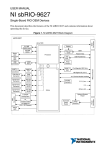
1
X3-SD User's Manual
X3-SD User's Manual
The X3-SD User's Manual was prepared by the technical staff of
Innovative Integration on March 19, 2009.
For further assistance contact:
Innovative Integration
2390-A Ward Ave
Simi Valley, California 93065
PH:
FAX:
(805) 578-4260
(805) 578-4225
email: [email protected]
Website: www.innovative-dsp.com
This document is copyright 2009 by Innovative Integration. All rights
are reserved.
VSS \ Distributions \ SD \ Documentation \ Manual \ SDMaster.odm
#XXXXXX
Rev 1.0
Table of Contents
X3-SD User's Manual................................................................................................................................2
Introduction................................................................................................................................................9
Real Time Solutions!...............................................................................................................................................................9
Vocabulary...............................................................................................................................................................................9
What is X3-SD? .........................................................................................................................................................10
What is Malibu? ........................................................................................................................................................10
What is C++ Builder?.................................................................................................................................................10
What is Microsoft MSVC?.........................................................................................................................................10
What kinds of applications are possible with Innovative Integration hardware?.......................................................10
Why do I need to use Malibu with my Baseboard?....................................................................................................11
Finding detailed information on Malibu.....................................................................................................................11
Online Help......................................................................................................................................................................11
Innovative Integration Technical Support........................................................................................................................11
Innovative Integration Web Site......................................................................................................................................12
Typographic Conventions......................................................................................................................................................12
Windows Installation...............................................................................................................................13
Host Hardware Requirements................................................................................................................................................13
Software Installation..............................................................................................................................................................13
Starting the Installation ...................................................................................................................................................14
The Installer Program.......................................................................................................................................................15
Tools Registration..................................................................................................................................................................17
Bus Master Memory Reservation Applet...................................................................................................................17
Hardware Installation.............................................................................................................................................................18
After Power-up......................................................................................................................................................................19
Installation on Linux...............................................................................................................................20
Package File Names...................................................................................................................................................20
Prerequisites for Installation..................................................................................................................................................20
The Redistribution Package Group - MalibuRed.............................................................................................................20
Malibu..............................................................................................................................................................................21
Other Software.................................................................................................................................................................21
Baseboard Package Installation Procedure............................................................................................................................21
Board Packages................................................................................................................................................................22
Unpacking the Package....................................................................................................................................................22
Creating Symbolic Links............................................................................................................................................22
Completing the Board Install...........................................................................................................................................23
Linux Directory Structure......................................................................................................................................................23
Applets........................................................................................................................................................................23
Documentation...........................................................................................................................................................23
Examples....................................................................................................................................................................23
Hardware....................................................................................................................................................................23
About the X3 XMC Modules..................................................................................................................24
X3 XMC Architecture...........................................................................................................................................................24
X3 Computing Core...............................................................................................................................................................26
X3-SD User's Manual
3
X3 PCI Express Interface......................................................................................................................................................28
Data Buffering and Memory Use...........................................................................................................................................29
Computational SRAM................................................................................................................................................29
Data Buffer SRAM.....................................................................................................................................................30
EEPROM....................................................................................................................................................................30
Digital I/O..............................................................................................................................................................................30
Software Support..............................................................................................................................................................30
Hardware Implementation................................................................................................................................................31
Digital I/O Timing............................................................................................................................................................32
Digital IO Electrical Characteristics................................................................................................................................32
Notes on Digital IO Use...................................................................................................................................................33
Serial EEPROM Interface......................................................................................................................................................34
Thermal Protection and Monitoring......................................................................................................................................35
Thermal Failures....................................................................................................................................................................36
LED Indicators.......................................................................................................................................................................37
JTAG Scan Path.....................................................................................................................................................................38
FrameWork Logic..................................................................................................................................................................38
Integrating with Host Cards and Systems..............................................................................................................................38
Writing Custom Applications.................................................................................................................40
X3-SD Snap Example............................................................................................................................................................40
Tools Required.................................................................................................................................................................40
Program Design................................................................................................................................................................41
The Host Application ............................................................................................................................................................41
User Interface...................................................................................................................................................................41
Logic Tab...................................................................................................................................................................41
Setup Tab....................................................................................................................................................................42
Analog Tab.................................................................................................................................................................42
ZbtRam Tab................................................................................................................................................................43
Host Side Program Organization.....................................................................................................................................43
ApplicationIo....................................................................................................................................................................44
Initialization................................................................................................................................................................44
Logic Loading............................................................................................................................................................47
Starting Data flow.......................................................................................................................................................48
Handle Data Required................................................................................................................................................51
EEProm Access..........................................................................................................................................................53
Developing Host Applications.................................................................................................................15
Borland Turbo C++................................................................................................................................................................15
Other considerations:.......................................................................................................................................................16
Microsoft Visual Studio 2005................................................................................................................................................17
DialogBlocks.........................................................................................................................................................................19
Summary................................................................................................................................................................................19
Applets......................................................................................................................................................20
Common Applets...................................................................................................................................................................20
Registration Utility (NewUser.exe).................................................................................................................................20
Reserve Memory Applet (ReserveMemDsp.exe)...........................................................................................................21
Data Analysis Applets...........................................................................................................................................................21
Binary File Viewer Utility (BinView.exe).......................................................................................................................21
Applets for the X3-SD Baseboard.........................................................................................................................................22
X3-SD User's Manual
4
EEProm............................................................................................................................................................................22
Finder...............................................................................................................................................................................23
Logic Loader .................................................................................................................................................................24
.........................................................................................................................................................................................24
PCI Configuration Utility (Config.exe)...........................................................................................................................24
MSDN Collection Integration Utility...............................................................................................................................25
X3-SD Hardware......................................................................................................................................26
Hardware Features.................................................................................................................................................................29
A/D Converters................................................................................................................................................................29
Input Range and Conversion Codes.................................................................................................................................30
Driving the A/D Inputs.....................................................................................................................................................31
Overrange Detection........................................................................................................................................................31
A/D Sampling Rates..............................................................................................................................................................31
Sample Rate Generation and Clocking Controls ..................................................................................................................32
External Clock and Reference Inputs..............................................................................................................................33
Generating a Sample Clock with the PLL........................................................................................................................35
PLL Status........................................................................................................................................................................38
PLL Interface...................................................................................................................................................................38
Notes About Programming the PLL................................................................................................................................40
Timing Analysis...............................................................................................................................................................41
Triggering .............................................................................................................................................................................41
Trigger Source..................................................................................................................................................................42
Framed Trigger Mode......................................................................................................................................................42
Decimation.......................................................................................................................................................................43
FrameWork Logic Functionality...........................................................................................................................................43
Power Controls and Thermal Design.....................................................................................................................................44
System Thermal Design...................................................................................................................................................44
Temperature Sensor and Over Temperature Protection..................................................................................................44
Reducing Power Consumption.........................................................................................................................................45
Alert Log................................................................................................................................................................................46
Overview..........................................................................................................................................................................46
Types of Alerts.................................................................................................................................................................46
Alert Packet Format.........................................................................................................................................................47
Software Support..............................................................................................................................................................47
Tagging the Data Stream..................................................................................................................................................48
Using the X3-SD....................................................................................................................................................................48
Where to start?.................................................................................................................................................................48
Getting Good Analog Performance..................................................................................................................................48
Application Logic.............................................................................................................................................................49
Calibration.............................................................................................................................................................................49
Production Calibration.....................................................................................................................................................49
Updating the Calibration Coefficients.............................................................................................................................50
Performance Data..................................................................................................................................................................51
Power Consumption.........................................................................................................................................................51
Environmental..................................................................................................................................................................51
Analog Input.....................................................................................................................................................................52
Connectors.............................................................................................................................................................................66
Input Connector JP1.........................................................................................................................................................66
XMC P15 Connector........................................................................................................................................................68
XMC P16 Connector........................................................................................................................................................72
X3-SD User's Manual
5
Note: PXI Express signals are only available when PXIE adapter card is used..............................................................75
Xilinx JTAG Connector...................................................................................................................................................76
Mechanicals...........................................................................................................................................................................77
X3-SD User's Manual
6
List of Tables
Table 1. X3 XMC Family......................................................................................................................................................25
Table 2. X3 XMC Family Peripherals...................................................................................................................................25
Table 3. X3 Computing Core Devices...................................................................................................................................26
Table 4. PCI Express Standards Compliance........................................................................................................................28
Table 5. Interfaces from PCI Express to Application Logic..................................................................................................29
Table 6. IUsesExtendedDioPort Class Operations................................................................................................................31
Table 7. Digital I/O Port Timing Parameters.........................................................................................................................32
Table 8. Digital IO Bits Electrical Characteristics................................................................................................................33
Table 9. Digital IO Clock Input Electrical Characteristics....................................................................................................33
Table 10. Temperature Alarms..............................................................................................................................................35
Table 11. X3 Modules FPGA JTAG Scan Path.....................................................................................................................38
Table 12. Development Tools for the X3-SD Example.........................................................................................................40
Table 13. X3-SD A/D Features..............................................................................................................................................29
Table 14. A/D Conversion Coding........................................................................................................................................30
Table 15. Sample Clock Modes.............................................................................................................................................32
Table 16. X3-SD External and Reference Clock Selection...................................................................................................34
Table 17. X3-SD External Clock and Reference Input Requirements..................................................................................35
Table 18. External Clock and Reference Signal Pinouts.......................................................................................................35
Table 19. PLL Interface Word Format..................................................................................................................................39
Table 20. PLL Read Sequence...............................................................................................................................................39
Table 21. PLL Read Word.....................................................................................................................................................40
Table 22. PLL Output Assignments......................................................................................................................................40
Table 23. X3-SD Conversion Clock Timing.........................................................................................................................41
Table 24. Reduced Power Options........................................................................................................................................45
Table 25. Alert Types............................................................................................................................................................46
Table 26. Alert Packet Format...............................................................................................................................................47
Table 27. X3-SD Power Consumption..................................................................................................................................51
Table 28. X3-SD Environmental Limits................................................................................................................................51
Table 29. X3-SD Analog Performance Summary.................................................................................................................52
Table 30. X3-SD XMC Connector P15 Pinout......................................................................................................................70
Table 31. P15 Signal Descriptions.........................................................................................................................................70
Table 32. X3-SD XMC Secondary Connector P16 Pinout....................................................................................................73
Table 33. P16 Signal Descriptions.........................................................................................................................................74
Table 34. X3-SD JP3 Xilinx JTAG Connector Pinout..........................................................................................................76
X3-SD User's Manual
7
List of Figures
Figure 1. Vista Verificaton Dialog........................................................................................................................................14
Figure 2. Innovative Install Program....................................................................................................................................15
Figure 3. Progress is shown for each section.........................................................................................................................16
Figure 4. ToolSet registration form.......................................................................................................................................17
Figure 5. BusMaster configuration........................................................................................................................................17
Figure 6. Installation complete..............................................................................................................................................18
Figure 7. X3 XMC Family Block Diagram...........................................................................................................................24
X3 Computing Core Block Diagram.....................................................................................................................................27
Figure 8. DIO Control Register (BAR1+0x14).....................................................................................................................31
Figure 9. Digital IO Port Addresses.......................................................................................................................................32
Figure 10. Digital I/O Port Timing........................................................................................................................................32
Figure 11. X3-SD Module.....................................................................................................................................................27
Figure 12. X3-SD Block Diagram.........................................................................................................................................28
Figure 13. X3-SD A/D Channel Diagram.............................................................................................................................30
Figure 14. X3-SD Clock Generation and Controls Block Diagram......................................................................................33
Figure 15. X3-SD External Clock Path.................................................................................................................................34
Figure 1. PLL Reference Prescaling......................................................................................................................................37
Figure 16. Analog Triggering Timing...................................................................................................................................42
Figure 17. X3-SD FrameWork Logic Data Flow..................................................................................................................43
Figure 18. X3-SD Ground Noise, Input Grounded, Fs = 48 ksps..........................................................................................57
Figure 19. X3-SD Frequency Response for 10 to 100 kHz...................................................................................................58
Figure 20. X3-SD Frequency Response, 0 to 200 kHz..........................................................................................................58
X3-SD A/D Signal Quality vs. Sample Rate ........................................................................................................................59
Figure 21. X3-SD A/D Signal Quality vs. Sample Rate........................................................................................................59
Figure 22. X3-SD A/D Signal Quality vs. Input Amplitude.................................................................................................61
Figure 23. Signal Quality, 1.1 kHz 9.9Vp-p differential, 52 ksps.........................................................................................63
Figure 24. Signal Quality, 1.01 kHz 19.8Vp-p input, 20 ksps...............................................................................................63
Figure 25. Signal Quality, 1 kHz 9.9Vp-p differential input, 100 ksps.................................................................................64
Figure 26. Signal Quality, 1.1 kHz 9.9Vp-p differential input, 216 ksps..............................................................................64
Figure 27. Intermodulation Distortion, 990 and 1100 dual tone, 100ksps............................................................................65
Figure 28. P15 XMC Connector Orientation.........................................................................................................................68
Figure 29. P16 XMC Connector Orientation.........................................................................................................................72
Figure 30. X3-SD J3 Orientation...........................................................................................................................................76
Figure 31. X3-SD J3 Side View............................................................................................................................................76
Figure 32. X3-SD Mechanicals (Bottom View) Rev B.........................................................................................................77
Figure 33. X3-SD Mechanicals (Top View) Rev B...............................................................................................................78
X3-SD User's Manual
8
X3-SD User's Manual
9
X3-SD Hardware
Introduction
The X3-SD is a member of the X3 XMC family that has 16 channels of 24-bit, 216 kSPS A/D conversion. The A/D
converter is a delta-sigma converter that has a usable dynamic range of over 105dB, making it ideal for acoustic and vibration
measurement applications.
A high performance computing core for signal processing, data buffering and system IO is built around a Spartan3 1M gate
FPGA. Supporting peripherals include 2MB of SRAM, conversion timebase and triggering circuitry, 44 bits digital IO, and
a PCI Express interface. The module format is a single slot XMC conforming to IEEE 1384 CMC standard and is compatible
with XMC.3 host sites.
Figure 1. X3-SD Module
Custom application logic development for the X3-SD is supported by the FrameWork Logic system from Innovative using
VHDL and/or MATLAB Simulink. Signal processing, data analysis, and application-specific algorithms may be developed
for use in the X3-SD logic and integrated with the hardware using the FrameWork Logic.
Software support for the module includes host integration support including device drivers, XMC control and data flow and
support applets.
X3-SD User's Manual
10
Figure 2. X3-SD Block Diagram
X3-SD User's Manual
11
Hardware Features
A/D Converters
The X3-SD has 16 channels of 24-bit A/D sampling at up to 216 kSPS using a four of Texas Instruments PCM4204 A/Ds.
The PCM4204 is a sigma-delta converter that has several operating modes allowing tradeoffs in filtering characteristics and
output data rates over a range of 12 ksps to 216 kSPS.
Feature
Description
Inputs
16, independent
Input Range
+10V to -10V, differential
Input Impedance
1K ohm || 15 pF (excludes cable)
A/D Devices
TI PCM4204
Output Format
2's complement, 24-bit
Number of A/D Devices
16 simultaneously sampling
Sample Rate
12-216 kSPS (lower rates use FPGA decimation)
Clock Rate
6.144 to 24.576 MHz
Calibration
Factory calibrated. Gain and offset errors are
digitally corrected in the A/D. Non-volatile
EEPROM coefficient memory.
Table 1. X3-SD A/D Features
Conversion clocking is provided through separate, special circuitry that minimizes jitter on the clocks. The clock circuitry
allows for a variety of clock sources, including two external sources, to be used as conversion timebases. See the clock
discussion for more details.
The following block diagram shows the general arrangement of the A/D. The differential inputs, from the front panel
connector, are adjusted for range through a differential amplifier and input to the A/D.
X3-SD User's Manual
12
Figure 3. X3-SD A/D Channel Diagram
Input Range and Conversion Codes
The input has a +10 to -10 V differential full scale input, 1K ohm input impedance. Other input ranges may be custom
ordered.
The output codes are 2's complement, 24-bit numbers.
Differential Input voltage (V+-V-)
Nominal Conversion Code (hex)
+10
0x7FFFFF
+5
0x400000
0V
0x000000
-5
0xA00000
-10
0x800000
Table 2. A/D Conversion Coding
X3-SD User's Manual
13
Driving the A/D Inputs
The X3-SD has fully differential inputs with 1K input impedance for the standard input range. The input range is specified as
a differential voltage or 10V from V+ to V- inputs, with a common mode voltage of 0V for full range.
The input signals should be driven differentially to realize the full performance of the A/D. The differential inputs reject
common mode noise from the system and the card itself to improve the conversion results. If you drive the inputs singleended, the results will be worse by at least 6dB in most cases, worse if the system noise is high.
For signal ended use, the unused input must be grounded. Input voltage range is limited to +5V to -5V for single-ended use
for the standard configuration.
The 1K input impedance requires that the signal source be capable of driving +/-10 mA for full scale inputs. The usual effect
of inadequate signal drive is increased distortion or, in the extreme case, loss of input range. This input impedance was
chosen as the best compromise between noise and input impedance. As the impedance goes up, the noise increases.
Overrange Detection
The A/D devices indicate when an overrange occurs on the input. Overrange occurs when the input signal is above the
+/-10V differential range is exceeded. For small overrange conditions of less than 5% overrange, the A/D will recover in a
few samples to proper readings. For larger overrange conditions, the A/D may require longer to recover.
The overrange indicator bit from each A/D can be used to trigger an alert in the logic to notify the application when this error
condition has occurred. The alert message shows when the overrange occurred in system time and which channels
overranged.
Custom logic has access to the overrange bits in the A/D interface component. Each data sample indicates when an overrange
occurs as part of its status byte appended to the data. This allows implementation of automatic gain controls for autoranging
external front end signal conditioning.
A/D Sampling Rates
The PCM 4204 supports output data rates from 12 ksps to 216 ksps on the X3-SD module. The PCM4204 has three output
rates: single, dual and quad. The data rates determine the oversampling used by the A/D filters as shown in the following
table. The A/D internal filters to provide faster data rates at the expense of dynamic range for the faster data rates.
Sample Rate (ksps)
Data Rate
Oversampling
A/D clock
rate (MHz)
12 to 54
Single
512
6.144 to
27.684
54 to 108
Dual
256
13.824 to
27.684
108 to 216
Quad
128
13.824 to
27.216
X3-SD User's Manual
14
Data rates lower than 12 ksps are supported using decimation in the logic. Decimation gives better performance than running
the A/D at low rates because conversion circuitry internal to the A/D cannot hold a signal long enough for a good conversion
result. The FrameWork Logic supports 1:N decimation resulting in lower data rates. All channels must be decimated at the
same rate.
Supporting software functions in the Malibu library automatically set the sample mode and clock rate required for the desired
sample rate. The single rate mode offers the best noise and dynamic range performance because more filtering is used. The
software always sets the converter to the lowest data rate mode possible to achieve the best performance.
Sample Rate Generation and Clocking Controls
The X3-SD can use a sample clock from the PLL, the PLL locked to an external clock, or an external clock. This allows the
module to be used in a variety of applications requiring either synchronization to a system clock or a software programmable
sample rates. All clock selections are software programmable on the module.
Clock Mode
Use for
Restrictions
Benefits
PLL with internal
reference
Software programmable
clock
Clock rate has tuning resolution of about 100
Hz
Low jitter clock provides best
dynamic performance
PLL with external
reference
Software programmable
clock referenced to
external clock input
External reference must be 1 to 100 MHz,
50-50 duty cycle, see electrical requirements
below
Lock to an external clock and
generate an A/D clock locked
to it; Clean up external clock
jitter using the PLL
External Clock
Synchronize sampling to
system devices
External clock must be 512,256 or 128 times
the sample rate corresponding to the FS
mode, 1 to 100 MHz, 50-50 duty cycle,
Lock to an external clock
Table 3. Sample Clock Modes
Note that an external clock used directly as the A/D clock must be a multiple of the sample rate corresponding to the
oversample rate of the A/D mode. The clock cannot be the output sample rate of the A/D.
The PLL can generate many sample rates that suit most applications. The advantage of using the PLL is that the sample
clock is very clean and provided the best AC performance. The output frequency of the PLL is programmable and is
determined by the reference clock rate and the VCO tuning range.
Software functions for PLL configuration, monitoring and clock distribution are provided in Innovative's Malibu software
toolkit that configure the operating mode and sample rate required for the desired A/D data rate. This takes into
consideration the A/D frequency limits, decimation factor in the A/D, and adjusts the PLL, when in use, to within its
specified operating range. In most applications, the supporting software sets the A/D clock rate according to the desired
sample rate, selecting the A/D mode for that sample rate.
X3-SD User's Manual
15
Figure 4. X3-SD Clock Generation and Controls Block Diagram
The PLL is software programmable and uses either fixed 24.576 MHz reference clock or an external reference clock. The
standard configuration for th PLL has a tuning range from 3.2 MHz to 30 MHz with about a 250 Hz resolution. The external
reference input further allows the PLL to generate a wide range of frequencies that can be synchronous to an external input.
External clock inputs allow other external clocks to be used for sample clocks for unique system integration requirements.
The sample clocks for the A/D devices are clocked directly from the clock distribution circuitry and are NOT derived from
the application logic clocks or PCI Express bus clock. This is because these clocks have too much jitter (phase noise) to use
for A/D conversion. The FPGA also receives a copy of the sample clock that is used for data capture and triggering.
Note: Conversion clocking is separate from triggering – sample clock is the time when samples are digitized, but trigger
determines when those samples are kept.
External Clock and Reference Inputs
The X3-SD has two external clocks that may be used for conversion timing plus two external inputs that can be used as a
reference to the PLL. The two external input clocks, Ext_Clk and PXI_DSTARA, can be used to directly clock the converters.
X3-SD User's Manual
16
The 24.575MHz clock oscillator and PXI_100M clock can be used as references to the PLL. The following table shows the
clock mux controls for the X3-SD.
Control Signal
Device
Function
Result
PLL_REF_SEL
PLL Reference Mux
Selects either PXI_100M or 24.576MHz fixed
oscillator as the PLL reference
0 = 24.576 MHz
1 = PXI_100M
PLL_CLKA_SEL
External Clock Mux
Selects either Ext_Clk or PXI_DSTARA as
input to the clock distribution
0 = Ext_Clk
1 = PXI_DSTARA
Table 4. X3-SD External and Reference Clock Selection
To use an external clock, the external clock multiplexer must be configured to select either the front panel external clock or
the PXI_DSTARA input on P16. The control signal, PLL_CLKA_SEL is from the application logic FPGA and is set by the
host software when the standard logic image is used. The external clock multiplexer output is the CLK1 input to the
AD9510, so the AD9510 must be configured to use CLK1 as the source to the output distribution section of the device. The
following diagram shows the clock path when an external clock is used.
Figure 5. X3-SD External Clock Path
The reference clock to the PLL is also software programmable. The external reference clock multiplexer must be configured
to select the reference clock to the PLL as either the 24.576 MHz oscillator or the PXI_100M input on P16. The control
X3-SD User's Manual
17
signal, PLL_REF_SEL is from the application logic FPGA and is set by the host software when the standard logic image is
used.
All external clock and reference inputs are LVDS and must be driven as a differential pair. Each differential pair is 100 ohm
terminated. The LVDS inputs cannot be driven single-ended – both inputs must be actively driven. Electrical characteristics
of the inputs are shown in the following table.
Parameter
Min
Typ
Max
Input Frequency
0
100 MHz
Input Common Mode Input Voltage
0.5V
2.4V
Input Amplitude
0.2
1Vp-p
Input Termination
100
Input Capacitance
15 pF
Comments
Larger inputs may cause damage.
Ohms
Table 5. X3-SD External Clock and Reference Input Requirements
The external clock and reference inputs are from either the front panel connector JP1 or XMC secondary connector P16. To
use the P16 connector inputs, it is necessary to have a carrier card that supports the P16 pinout shown later in this chapter.
Here is where the external clock inputs are connected:
Signal
Connector + Input
- Input
Comments
External Clock (Ext_clk)
JP1
33
67
MDR68 front panel connector
PXI_DSTARA
P16
A9
B9
XMC secondary connector
PXIE_100M
0.2
D9
E9
P16 connector
Table 6. External Clock and Reference Signal Pinouts
Generating a Sample Clock with the PLL
The PLL is configured to provide clock rates as shown in the following table. This table is based upon a 24.576 MHz
reference clock to the PLL and a VCO operating range of 77 to 111 MHz. As is evident, a wide range of sample rates can be
generated with the PLL using its tuning and post-dividers. Custom configurations with a different reference clock can be
ordered to meet exact requirements.
The PLL has two modes: fixed divider (FD) and dual modulus (DM). The FD mode does not use the A counter.
The tuning equation is
Fvco = (Fref/R) x (PB +A)
where
Fref = 24.576 MHz (or external reference frequency)
R = 1 to 16383, integers
B= 3 to 8191, integers; 1 = bypass
A= 0 to 63, integers, used only in dual modulus mode
X3-SD User's Manual
18
P= reference prescaling, shown in the following table for the two modes
and 77 MHz < Fvco < 111 MHz
Figure 1. PLL Reference Prescaling
The following table shows a sampling of the PLL output frequencies for a a desired frequency. This table does not show all
possible combinations of values and there may be settings closer to a particular frequency of interest. The table is a good just
illustrates the frequency range required by the A/D and the tuning resolution. In use, the Malibu software drivers compute
the required PLL configuration to come as close as possible to the desired sample rate considering the constraints of the
devices.
X3-SD User's Manual
19
Fvco = (Fref/R) x (PB +A)
Fs (Mhz)
27.684
27.683
26.000
23.000
22.000
21.000
20.000
19.000
18.000
17.000
16.000
15.000
14.000
13.000
12.000
11.000
10.000
9.000
8.000
7.000
6.000
5.000
4.050
4.001
4.000
D
4
4
4
4
4
4
4
6
6
6
6
6
6
8
8
8
8
10
12
12
14
16
20
24
24
FVCO
110.74
110.73
104
92
88
84
80
114
108
102
96
90
84
104
96
88
80
90
96
84
84
80
81
96.02
96
Fref (Mhz)
24.576
24.576
24.576
24.576
24.576
24.576
24.576
24.576
24.576
24.576
24.576
24.576
24.576
24.576
24.576
24.576
24.576
24.576
24.576
24.576
24.576
24.576
24.576
24.576
24.576
R
16383
16383
16383
16383
16383
16383
16383
16383
16383
16383
16383
16383
16383
16383
16383
16383
16383
16383
16383
16383
16383
16383
16383
16383
16383
PB+A
73819
73816
69329
61329
58663
55996
53330
75995
71995
67995
63996
59996
55996
69329
63996
58663
53330
59996
63996
55996
55996
53330
53996
64012
63996
P
32
32
32
32
32
32
32
32
32
32
32
32
32
32
32
32
32
32
32
32
32
32
32
32
32
A
27
24
17
17
7
28
18
27
27
27
28
28
28
17
28
7
18
28
28
28
28
18
12
12
28
B
2306
2306
2166
1916
1833
1749
1666
2374
2249
2124
1999
1874
1749
2166
1999
1833
1666
1874
1999
1749
1749
1666
1687
2000
1999
FS ACTUAL (Mhz)
27.683815
27.682690
25.999962
22.999779
21.999968
20.999782
19.999971
18.999910
17.999849
16.999788
15.999977
14.999916
13.999854
12.999981
11.999982
10.999984
9.999985
8.999949
7.999988
6.999927
5.999938
4.999993
4.049947
4.000994
3.999994
Error (ppm)
-6.7
-11.2
-1.5
-9.6
-1.5
-10.4
-1.5
-4.8
-8.4
-12.5
-1.5
-5.6
-10.4
-1.5
-1.5
-1.5
-1.5
-5.6
-1.5
-10.4
-10.4
-1.5
-13.0
-1.4
-1.5
Illustration 1: X3-SD PLL Output Frequencies
PLL Status
The PLL has a status pin that can be programmed to show when the PLL is locked, or other status information. The software
in the SNAP example configures this pin to be digital lock detect. It indicates when the PLL is locked and ready for use. If
the PLL lock is false, the PLL is not working properly and may give poor results or inaccurate frequencies. Even when the
PLL is unable to lock, it will produce an output so the mere presence of data does not indicate that the PLL is operating at the
correct frequency or is stable.
The PLL lock can also generate an alert to the system if an unlock condition occurs. In this mode, when the PLL falls out of
lock, as indicated by a falling edge on the PLL status pin an alert message is created showing the time of the unlock and other
system information. See the Alert Log section for further information on using Alerts.
PLL Interface
The AD9510 is mapped into the PCI Express memory space for its control port at BAR1+0xA so that the host can perform
configuration. Writes to the PLL interface port generate a serial data stream to the PLL that is used to configure the PLL.
X3-SD User's Manual
20
Writes to the PLL are performed when the PLL interface port is written to. Reads from the PLL require a two step process
consisting of first a write to the PLL register specifying a read at an address, followed by a read from the PLL register that
returns the value of the PLL register specified by the address in the PLL word. The PLL is read is a single byte.
This interface is only for configuration, accesses should be spaced by the host computer to be at least 2 ms apart. The
Malibu library handles this restriction as part of the function.
The PLL interface uses a 24-bit word to communicate with the PLL that specifies a read or write access, the PLL register
address and the data byte to transfer. For reads, the data byte is a don't care. The 24-bit word is as follows.
Bits
Function
31..24
Not Used.
23
R/W; 1 = read PLL.
22..15
X“00”
14..8
PLL register address.
7..0
Data byte (don't care for reads)
Table 7. PLL Interface Word Format
For reads, the PLL must be written to with a bit 23 as '1' and the address that is to be read, then read from the PLL register.
For example, a read to PLL register X”40” would be performed as
Step
Read/Write
Address
Value
Comments
1
Write
BAR1+0xA
X”00804000”
Set up a read from PLL address X”40”
2
Read
BAR1+0xA
X”x01303xx”
See format below
Table 8. PLL Read Sequence
The PLL readback word has the following format. The PLL read must be performed before any additional writes are
performed.
X3-SD User's Manual
21
Bits
Function
31
PLL Status Pin
30..24
“0000000”
23..8
X“1303”
7..0
Data byte (don't care for reads)
Table 9. PLL Read Word
Notes About Programming the PLL
The PLL, an Analog Devices AD9510, must be initialized prior to use. This device has many configurations that require
programming of a large number of registers prior to use. The X3-SD support software provides PLL configurations that
satisfy most applications and should be used if possible.
For custom configurations, the AD9510 data sheet should be consulted. The X3-SD uses the AD9510 for five output clocks
– one for each A/D channel plus one for the FPGA. These clocks are connected as shown in the following table. The
FrameWork Logic is predicated on the all of the channels operating synchronously, therefore the AD9510 is programmed so
that all channels have the same clock output with the same phase. The PLL should be programmed to use these outputs with
the signal type noted.
Channel
AD9510 Output
Signal Type
FPGA
Channel 0
LVPECL
A/D 0
4+
CMOS
A/D 1
5+
CMOS
A/D 2
6+
CMOS
A/D 3
7+
CMOS
Table 10. PLL Output Assignments
The VCO used with the AD9510 has a tuning range of 77 to 111 MHz and is connected to the CLK2 input to the PLL. The
standard reference clock is 24.576 MHz to the PLL, although an external reference may be used. The output of the PLL
section of the AD9510 can therefore be programmed to many numbers in the range of 77 to 111 MHz, that may be
subsequently divided in the PLL outputs. The dividers in the clock distribution section of the AD9510can be used to further
divide the clock by 1 to 32, with the restriction only even numbers are used to make the clock a 50% duty cycle.
The external clock and optional fixed oscillator are connected to the CLK1 input. The PLL must be programmed to use one
of these two clock sources for the outputs. The clock dividers on the outputs should be programmed to the same divisor to
work with the standard logic.
The AD9510 is programmed during initialization of the card. All configuration registers are written, then an update
command is sent to the PLL that makes the outputs update simultaneously. After an update, the clock is stable when the PLL
status bit indicates a lock, but the A/Ds require additional time to stabilize so a 1 ms period should be allowed for stabilizing
the clock.
X3-SD User's Manual
22
Timing Analysis
There are several timing parameters associated with the clock control circuitry that affect the measurement process. The
following table summarizes two important effects.
Timing propagation delay through the logic for external clocks are shown for the maximum and typical timing. The external
clocks go through one or two multiplexers, accounting for the differences in propagation delay to the various devices.
Jitter to the A/D converters is of primary interest since that limits the A/D conversion accuracy. Jitter is summed as the root
sum of squares for random jitter.
Table 11. X3-SD Conversion Clock Timing
Clock Source
Clock Destination
Propagation Delay (ns)
Additive Jitter
(ps RMS)
External clock or
PXI_DSTARA
A/D conversion clock
1.8 typical
2.5 maximum
0.05
24.576 MHz or PXIE_100M
PLL Reference clock
1.2 typical
1.5 maximum
0.05
Triggering
The X3-SD has a trigger control component in the FPGA that controls the data acquisition process. The sample clock
specifies the instant in time when data is sampled, whereas triggering specifies when data is kept. This allows the application
to collect data at the desired rate, and keep only the data that is required.
On the X3-SD module, all A/D channels operate synchronously using the same clock and trigger. The trigger controls
allows data to be acquired continuously, or during a specified time, as triggered by either a software or external trigger. Data
can also be decimated to reduce data rates.
Trigger Mode
Data Collected/Played Back
Start Trigger
Stop Trigger
Continuous
All enabled channel pairs
Software or rising edge of
external trigger
Software or falling edge of
external trigger
Framed
N sample points for each of
the enabled channel pairs
Software or rising edge of
external trigger
Stops when N samples are
collected back
Decimation
M points are discarded for
every point kept. May be
used with either trigger
mode.
-
-
Table 1: Trigger Modes
On the X3-SD module, the sample rate is a fraction of the A/D clock rate because the A/D uses multiple clocks for its
conversion process. The effective sample rate, Fs, is a sub-multiple of the A/D clock rate. The trigger component operates at
X3-SD User's Manual
23
the sample rate for its data collection process. So even though a 100 ksps data from the A/D may use a 24.576 MHz A/D
clock, the trigger components collects the data based upon the 100 ksps data rate.
Fs
Trigger
Analog
Input
Samples are acquired for each sample period when
trigger is true.
Figure 6. Analog Triggering Timing
As shown in the diagram, samples are captured when the sample period and the trigger are true. For the X3-SD, the sample
clock to the A/D is a multiple of the sample rate, as determined by the decimation setting in the A/D so the left/right period
signal is used for this purpose. This insures that the trigger gets a coherent data set (all channels sampled at the same time). The
trigger is true in continuous mode after a rising edge on the trigger input, software or external, until a falling edge is found.
The trigger is timed against the sample clock and may have a 0 to +1 A/D sample uncertainty for an asynchronous trigger
input.
The trigger control on the X3-SD module always ensures that a complete set of A/D samples for the time period are acquired
no matter when the trigger is deasserted. This means that for an unsynchronized trigger input such as an external device, you
will always get samples for all enabled channels no matter when trigger is enabled or disabled.
Trigger Source
A software trigger or external trigger can be used by the trigger controls. Software trigger can always be used, but external
triggering must be selected. The trigger source is level-sensitive for the continuous mode or edge-triggered for the framed
mode triggering.
The Malibu software tools provide trigger source configuration and methods for software triggering, retriggering in framed
mode and trigger mode controls.
Framed Trigger Mode
Framed trigger mode is useful for collecting data sets of a fixed size each time the input trigger is fired. In framed mode, the
trigger goes false once the programmed number of points N have been collected. Start triggers that occur during a frame
trigger are ignored.
X3-SD User's Manual
24
The maximum number of points per frame is 16,777,216 (2^24) points, while the minimum number of points is 2.
Data flow to the host is independent of the framed triggering mode. In most cases, packet sizes to the host are selected to be
integer submultiples of the frame size to allow the entire data set to flow to the host. That way, the entire data frame can be
moved immediately to the host without waiting for the next trigger frame.
Decimation
The data may be decimated by a programmed ratio to reduce the data rate. This mode is usually used when the data rate is less
than the minimum sample rate of the A/D (12 kHz). We recommend using decimation if the data rate falls below 12 ksps that
decimation be used because the A/D performance begins to degrade below this output data rate.
The decimation simply discards N points for every point kept – no averaging or filtering is used. When decimation is true, the
number of points captured in the framed mode is the number of decimated points, in other words the discarded points do not
count. Maximum decimation rate is 1/4095.
When decimation is used in the framed trigger mode, the number of points captured is after decimation. The frame count is
always the actual number of points inserted into the FIFO.
FrameWork Logic Functionality
The FrameWork Logic implements a data flow for the X3-SD that supports standard data acquisition functionality. This data
flow, when used with the supporting software, allows the X3-SD to act as a data acquisition card with 2MB of data buffering
and high speed data streaming to the host PCI Express. The example software for the X3-SD demonstrates data flow control,
logic loading and data logging.
Figure 7. X3-SD FrameWork Logic Data Flow
X3-SD User's Manual
25
The data flow is driven by the data acquisition process . Data flows from the A/D devices into the A/D interface component
in the FPGA as they are acquired as controlled by the triggering. The data is then error corrected and the enabled channels
are stored into the data buffer, which is implemented a data queue in the SRAM. When data is available in the buffer, the
packetizer pulls data from the queue, creates data packets of the programmed size and sends those to the PCIe interface logic.
From here, the Velocia packet system controls the flow of data to the host. Data packets flow into host memory for
consumption by the host program.
The Board Basics and Host Communications chapters of this manual discuss the use of the packet data system used on the
X3 module family. The X3-SD module FrameWork Logic connects the data from A/D interface to the packet system by
forming the data into 32-bit words of consecutive enabled channels. Status indicators for the A/Ds are integrated with the
alert log to provide host notifications of important events for monitoring the data acquisition process, some of which are
unique to the X3-SD.
The complete description of the FrameWork Logic is provided in the FrameWork Logic User Guide including the memory
mapping, register definitions and functional behavior. This logic is about 50% of the available logic in the application FPGA
(1M gate device). In many custom applications, unused logic functions can be deleted to free up gates for the new
application.
Power Controls and Thermal Design
The X3-SD module has temperature monitoring and power controls to aid in system integration. Also, the module has been
designed to include conduction cooling to improve heat dissipation from the module. These features can make the module
more reliable in operation and also reduce power consumption.
System Thermal Design
The X3-SD dissipates about 12.2 Watts typically for all A/D channels running at full rate.
Forced air cooling or conduction cooling is required in most installations, including operation in a room temperature
environment (27C). An air flow of 5 CFM is sufficient to cool the module under most lab conditions. If the environment is
more demanding, you will need to carefully consider how to cool the module. Forced air cooling is used in may compact PCI
installations and this is very effective.
If forced air cooling is not used, conduction cooling is another method of dissipating the module heat. A thermal plane in the
card is attached to the center stripe on the card. The card can then be cooled by mounting the card on host card that supports
conduction cooling. The conduction cooling method allows the module heat to be flowed out to the chassis. The thermal
plane has NO electrical connection in the module and cannot be used as a ground.
The front panel bracket is used for cooling and is attached to the thermal plane.
Temperature Sensor and Over Temperature Protection
The temperature sensor is described in detail in the Board Basics chapter of this manual. The temperature sensor is used to
monitor the module temperature and protect it from overheating. Temperature readings from the module are provided for
X3-SD User's Manual
26
system monitoring and are also reported in each alert packet. During system development, it is a good idea to have a look at
the temperature and verify that everything is OK inside the system during actual use.
When the module exceeds 85C, the analog power supplies shut down, reducing the power consumption to about 3W. The
module can continue to communicate but no valid data will be collected. A temperature warning may be enabled via the
Alert Log when the temperature is above 70C. If a warning occurs, it is best to do something either to reduce power
consumption, such as tunning off the A/D channels, turning on a system fan or turning off other things in the system.
The application LED on the X3-SD will flash when the module is too hot (>85C). It must be turned off to restart the module
once a failure occurs.
Reducing Power Consumption
The X3-SD has power controls that allow the application software to power down unused channels and run in reduced power
mode for the A/Ds. If you incorporate these into your application, you may be able to avoid problems later in hot
installations.
Feature
Power Saved
Comments
A/D Channel Disabled**
0.4W/ channel pair
PLL power down
0.3W
PLL off – must use external clock
Application FPGA not
configured
1.5W
Must reload the FPGA to resume operation.
33 MHz system clock
0.5
33 MHz FPGA system clock. Data rate to host
is limited to <100 MB/s typically.
Allow warm-up time of 1 minute for best
performance
Table 12. Reduced Power Options
** Must disable two adjacent channels 0/1, 2/3 etc.
The A/D power controls are under software control. In the example software, only the enabled A/D channels are turned on to
save power.
The 33 MHz system clock feature requires that the card reconfigured by installing a 0 ohm jumper for R228. This jumper is
located near the PCIe interface device (XIO2000A) and is on the back of the card. The factory can pre-configure this if you
decide to use this option in production. As shipped, the system clock is 66 MHz because this allows the system logic to
support custom logic developers more easily. Tests have shown that this reduces operating temperature by 4 C for room
temperature testing with no forced air. Total data rate from the module must be limited to 50MB/s when a 33 MHz clock is
used.
X3-SD User's Manual
27
Alert Log
Overview
X3 modules have an Alert Log that can be used to monitor the data acquisition process and other significant events. Using
alerts, the application can create a time history of the data acquisition process that shows when important events occurred
and mark the data stream to correlate system events to the data.. This provides a precision timed log of all of the important
events that occurred during the acquisition and playback for interpretation and correlation to other system-level events. Alerts
for critical system events such as triggering, data overruns, analog overranges, and thermal warnings provide the host system
with information to manage the module.
The Alert Log creates an alert packet whenever an enabled alert is active. The packet includes information on the alert, when
it occurred in system time, and other status information. The system time is kept in the logic using a 32-bit counter running
at the sample clock rate. Each alert packet is transmitted in the packet stream to the host , marked with a Peripheral Device
Number corresponding to the Alert Log.
The Alter Log allows X3 modules to provide the host system with time-critical information about the data acquisition to allow
better system performance. System events, such as over-ranges, can be acted on in real-time to improve the data acquisition
quality. Monitoring functions can be created in custom logic that triggers only when the digitized data shows that something
interesting happened. Alerts make this type of application easier for the host to implement since they don't require host activity
until the event occurs.
Types of Alerts
Alerts can be broadly categorized into system, IO and software alerts.
System alerts include monitoring functions such as temperature, time stamp rollover and PLL lost. These alerts just help keep
the system working properly. The temperature warning should be used increase temperature monitor and to prepare to shut
down if necessary because thermal overload may be coming. Better to shut down than crash in most cases. The temperature
failure alert tells the system that the module actually shut itself down. This usually requires that the module be restarted when
conditions permit.
The data acquisition alerts, including over ranges, overflows and triggering, tell the system that important events occurred in
the data acquisition process. Overflow is particularly bad – data was lost and the system should try to alleviate the system by
unclogging the data pipe, or just start over. If you get an overrange alert, then the data may just be bad for a while but
acquisition can continue. Modules with programmable input ranges can use this to trigger software range changes.
Software alerts are used to tag the data. Any message can be made into an alert packet so that the data stream logged includes
system information that is time-correlated to the data.
Table 13. Alert Types
Alert
Timestamp rollover
Software Alert
Over Temperature Alarm/ Sensor Failure
X3-SD User's Manual
Purpose
The 32-bit timestamp counter rolled over. This can be used to extend the
timestamp counter in software.
The host software can create alerts to tag the data stream.
The module temperature exceeded 85C.
28
Temperature Warning
PLL Lost
ADC Queue Overflow
ADC Trigger
ADC Overrange
The module temperature exceeded 70C.
The sample clock PLL lost lock. The PLL must be reconfigured.
The ADC data queue overflowed indicating the the host did not consume
the data quickly enough.
The ADC trigger went active.
An ADC channel was overranged.
Alert Packet Format
Alert data packets have a fixed format in the system The Peripheral Device Number (PDN) is programmable in the software
and is included in the packet header, thus identifying the alert data packets in the data stream. The packet shows the
timestamp in system time, what alerts were signaled and a status word for each alert.
Dword #
0
1
2
3
4
5
6
7
10..8
12
35..13
Description
Header 1: PDN & Total #, N, of Dwords in packet ( e.g. Headers + data payload )
Header 2: 0x00000000
Alerts Signaled
Timestamp
0
Software Word
temp_sensor_error & temp_error & "00" & X"000" & temp_data;
temp_warning & "000" & X"000" & temp_data;
0
X"1303000" & "000" & mq_overflow(0);
unused
Table 14. Alert Packet Format
Since alert packets contain status words such as temperature for each packet, a software alert can essentially be used to read
temperature of the module and so that it can be recorded.
Software Support
Applications have different needs for alert processing. Aside from the bulk movement of data, most applications require some
means of handling special conditions such as post-processing upon receipt of a stop trigger or closing a driver when an
acquisition is completed.
When the alert system is enabled, the module logic continuously monitors the status of the peripheral (usually analog)
hardware present on the baseboard and generates an alert whenever an alert condition is detected. It's also possible for
application software to generate custom alert messages to tag the data stream with system information.
X3-SD User's Manual
29
The Malibu software provides support for alert configuration and alert packet processing. See the software manual for usage.
Tagging the Data Stream
The Alert Log can be used to tag the data stream with system information by using software alerts. This helps to provide systemlevel correlation of events by creating alert packets in the data stream created by the host software. Alert packets are then created by
the X3 module and are in the stream of data packets from the module. For example it is often interesting when something happens
to the unit under test, such as a change in engine speed or completion of test stimulus.
Using the X3-SD
Where to start?
The best place to start with the X3-SD module is to install the module and use the SNAP example to acquire some data. This
program lets you log data from the module and use all the features like triggering, clocks, alerts and calibration ROM. You
can use this program to acquire some data and log it to disk. This should let you verify that the module can acquire the data
you want and give you a quick start on deciding what sample rates to use, how to trigger the data acquisition best for your
application, and just get familiar with using the module.
The program also shows how to use BinView, a data analysis and viewing program by Innovative, that will let you see what
you acquired in detail. Both time domain and frequency domain data can be viewed and analyzed. Data can also be exported
to programs like Excel and MATLAB for further analysis.
Before you begin to write software, taking a look at SNAP will allow you see everything working. You can then look at the
code for SNAP and modify it for your application or grab code from it that is useful.
Getting Good Analog Performance
The X3-SD has a dynamic range exceeding 100 dB. To take advantage of this, it is important to do the following
●
Use differential signals to eliminate system noise. Single-ended signals give typically 10 to 20 dB worse
results because of noise pickup.
●
Band limit input signals. Even though the A/D has filtering and rejects most out-of-band noise, it is a good
idea to filter the incoming signal just to get rid of as much noise as possible.
●
Scale your input signals to be +/-10V full scale. Make the signal as big as possible so that the noise is a not as
much a factor. Custom ranges can be ordered if necessary.
●
Use a high quality shielded cable. The MDR68 cable was selected because it has a foil shield and delivers
near-coax performance.
●
Reference input signals to the module ground. Be sure not to introduce ground loops.
X3-SD User's Manual
30
●
Provide sufficient signal strength to drive the input. The X3-SD has about 1K input impedance. Be sure you
can drive this load without distorting your signals.
If you decide to test the X3-SD to verify its performance, be aware that most signal sources are not good enough without
additional filtering and careful use. Most single-ended lab instruments are limited by their distortion to about 90 dB. Postfilter is necessary to clean them up if you want to test the X3-SD.
Application Logic
The application logic must be loaded after every system boot-up or reset. There is no on-card storage for the logic image.
The logic can be loaded using the LogicLoad software applet or is loaded as part of the application itself, such as SNAP. If
you write your own application, you will need to either use LogicLoad or incorporate a logic loader in the application. The
code in SNAP is a good example of how to do this.
Calibration
Every A/D sample is error corrected on the X3-SD module in real-time by the application FPGA. This error correction is
done as the samples flow through the FPGA and is done digitally. This results in improved performance and reliability for the
module because the error correction does not change over time or temperature.
The basic error terms for offset and scale factor are corrected by the logic. This is a first order error correction where
y = mx + b
wherein x = the input sample, m = gain correction and b = offset correction. The resultant samples are the error corrected
output samples. Trim range is about 1.5 for gain and 10% for offset.
Production Calibration
Each X3-SD is calibrated as part of the production tests performed. The calibration results are provided on the production test
report with each module. The results of the calibration are stored in the on-board EEPROM memory. These calibration
values are used by the logic to correct the analog errors and are loaded into the A/D as part of the initialization by the
software.
The calibration technique used determines the A/D errors by first measuring the output with ground connected, then a known
voltage. A value close to full scale such as 9.8V and -9.8V are recommended. The measurements are the average of 64K
samples at each test voltage. From these three points across the input range, the gain and offset errors are calculated.
All test voltages are measured as part of the procedure with NIST traceable equipment. Production calibration is performed at
room temperature (~27C) with the module operating temperature at about 50C.
Under normal circumstances, calibration is accurate for one year. For recalibration, the module can be sent to Innovative or
recalibrated using a similar test procedure.
X3-SD User's Manual
31
Updating the Calibration Coefficients
A software applet for writing the calibration coefficients to the EEPROM is provided (EEPROM.exe). New coefficients are
simply typed into the offset and gain field for each channel.
Calibration coefficients for gain should not be greater than 1.1 and offset < 0x8000 . If the calculated coefficients are larger
than this, they are either wrong or the channel is damaged.
X3-SD User's Manual
32
Performance Data
Power Consumption
The X3-SD requires the following power for typical operation with when using the FrameWork Logic. This typical number
assumes a 67 MHz system clock rate and 216 KSPS A/D data rates for the application logic.
Table 15. X3-SD Power Consumption
Voltage
Maximum Allowed
Current (A)
Typical Current
Required (A)
Typical
Derived from
Power (W)
Supplies these Devices
3.3V
5A
(recommended)
3.7
12.2
Direct connect to the
PCIe host
All devices; on-card power
supplies use 3.3V as source
12V
-
0
0
Not required
-
Total
Power
12.2
Surge currents occur initially at power-on and after application logic initialization. The power-on surge current lasts for
about 10 ms @ 5A on the 3.3V supply. This surge is due primarily to charging the on-card capacitors and the startup current
of the FPGAs. After initial power-up, the logic configuration will also result in a step change to the current consumption
because the logic will begin to operate. In our testing and measurements, this has not been a surge current as much as a just a
step change in the power consumption.
Power consumption varies and is primarily as a function of the logic design. Logic designs with high utilization and fast
clock rates require higher power. Since calculating power consumption in the logic requires many details to be considered,
Xilinx tools such as XPower are used to get the best estimates.
It is important that any custom logic design have a substantial safety margin for the power consumption. Allowance for
decreased power supply efficiency due to heating can account for 10% derating. Also, dynamic loads should be considered so
that peak power is adequate. In many cases a factor of two for derating is recommended.
Environmental
Table 16. X3-SD Environmental Limits
Condition
Operating Temperature
X3-SD User's Manual
Limits
0 to 55 C
(65C as measured by the on-card temp sensor)
33
Condition
Limits
Humidity
5 to 95 %, non condensing
Storage Temperature
-30 to 85 C
Forced Air Cooling
Forced air cooling required with a minimum of
5 CFM for 27C ambient.
Vibration, operating
ETS 300 019- 1.3 [R3], class 3.3
Vibration, storage
ETS 300 019- 1.1 [R1], class 1.2
Vibration, transportation
ETS 300 019- 1.2 [R2], class 2.3
except for free-fall: class 2.2
Analog Input
A summary of the analog performance follows for the X3-SD module.
All tests performed at room temperature, with no forced air cooling unless noted. Test environment was PCIe adapter card in
PC running testbed software using FrameWork Logic.
Table 17. X3-SD Analog Performance Summary
Test Group
Analog Input
Accuracy
Analog Input
Analog Input
Parameter
Bandwidth
Measured
Units
Test Conditions
0.4dB
dB
0 to 100 kHz
-100
dB
200 kHz
Impedance
1k
Ohms
nominal
Input Range
Max =+/-10.02
Min = +/-9.98V
Vp-p
differential
Standard on X3-SD, calibration results may limit input
range to 97% of full scale nominal.
Offset
<100
uV
Factory calibration, average of 64K samples
Gain
<0.2
%
Factory calibration, average of 64K samples
Ground Noise
70
uVp-p
Input Grounded, Fs = 52 ksps, 250k samples
Ground Noise
-140
dB
Input Grounded, Fs = 52 ksps, 64K sample FFT, nonaveraged
Crosstalk
-100
dB
1 MHz, 20Vp-p input, cable included, all channels
Common
Mode
Rejection
-80
dB
1k Hz, 9.9Vp-p differential
X3-SD User's Manual
34
Test Group
Analog Input
Parameter
Amplitude
Variation
Measured
0.4
Units
dB
Test Conditions
10 Hz to 100K Hz input range, 9.9Vp-p differential
Noise Floor: grounded input.
Figure 8. X3-SD Ground Noise, Input Grounded, Fs = 48 ksps
X3-SD User's Manual
35
Frequency Response
Test method: Input sine from 10 to 200 kHz at 10V differential
Frequency Response
1.0
0.8
0.6
0.4
0.2
0.0
dB
-0.2
-0.4
-0.6
-0.8
-1.0
10
100
1000
10000
100000
Hz
Figure 9. X3-SD Frequency Response for 10 to 100 kHz
Frequency Response
10.0
0.0
-10.0
-20.0
dB
-30.0
-40.0
-50.0
-60.0
1E+1
1E+2
1E+3
1E+4
1E+5
Hz
Figure 10. X3-SD Frequency Response, 0 to 200 kHz
X3-SD User's Manual
36
X3-SD A/D Signal Quality vs. Sample Rate
Fs
kHz
S/N
dB
10
104.5
20
110.4
44.1
111.1
48
100.3
64
100.4
Figure 11. X3-SD A/D Signal Quality vs. Sample Rate
SFDR
dB
ENOB
bits
100.2
105
103.7
102.3
103
THD
dB
15.6
16.1
16.1
15.4
15.5
S/N vs Sample Rate
-99.6
-101.1
-101.3
-100.2
-102.2
ENOB vs Sample Rate
115
18.0
17.5
110
17.0
16.5
dB
S/N
100
bits
105
16.0
ENOB
15.5
15.0
95
14.5
90
14.0
0
10
20
30
40
50
Sample Rate (kHz)
X3-SD User's Manual
60
70
0
10
20
30
40
50
60
70
Sample Rate(kHz)
37
SFDR vs Sample Rate
THD vs Sample Rate
-90
109
-92
107
-94
-96
105
dB
SFDR
dB
-98
103
-100
101
-102
99
-104
THD
-106
97
-108
95
-110
0
10
20
30
40
50
60
Sample Rate (kHz)
X3-SD User's Manual
70
0
10
20
30
40
50
60
70
Sample Rate (kHz)
38
Figure 12. X3-SD A/D Signal Quality vs. Input Amplitude
X3-SD User's Manual
Vin
Vp-p
S/N
db
SFDR
dB
ENOB
bits
THD
dB
0.1
0.2
0.3
0.4
0.5
0.6
0.7
0.8
0.9
1
2
3
4
5
6
7
8
9
9.9
10
12
14
16
18
19
19.9
69.1
75.1
78.3
80.8
82.9
84.5
85.8
87.2
88.1
89.2
95.7
94.3
96.8
98.8
100.8
102.1
103.7
104.8
105.2
105.5
110.4
115.7
110.8
119.5
120.1
117.1
93.4
96.3
92.9
95.5
97.8
99
99.5
101.4
102.7
104.3
109.2
103.4
105.7
108
109.2
110.8
111.2
112.6
112.4
112.2
109.2
102.4
99.5
97.9
97.3
96.8
11.1
12.1
12.7
13.1
13.4
13.7
13.9
14.1
14.2
14.4
15.3
15.1
15.5
15.8
16
16.1
16.2
16.4
16.4
16.5
16.3
15.9
15.5
15.5
15.4
15.3
-99.8
-102.3
-105.4
-106.7
-108.1
-110.2
-110.5
-109
-109.2
-110.4
-109.7
-108.2
-110.1
-110.5
-109.1
-108.3
-107.2
-108
-107.5
-108.4
-103.3
-98.9
-96.8
-95.4
-94.7
-94.3
39
SFDR vs Input Amplitude
S/N vs Input Amplitude
120
150
115
140
130
110
120
105
100
S/N
dB
dB
110
100
SFDR
95
90
80
90
70
85
60
80
50
0
2
4
6
0
8 10 12 14 16 18 20
2
4
6
8 10 12 14 16 18 20
Vin
Vin
Note: All measured using 9.9Vp-p differential inputs
THD vs Input Amplitude
18
-80
17
-85
16
-90
15
-95
14
ENOB
dB
bits
ENOB vs Input Amplitude
-100
13
-105
12
-110
X3-SD User's Manual
11
THD
40
-115
10
-120
0
2
4
6
8 10 12 14 16 18 20
Vin
0
2
4
6
8 10 12 14 16 18 20
Vin
Figure 13. Signal Quality, 1.1 kHz 9.9Vp-p differential, 52 ksps
Figure 14. Signal Quality, 1.01 kHz 19.8Vp-p input, 20 ksps
X3-SD User's Manual
41
Figure 15. Signal Quality, 1 kHz 9.9Vp-p differential input, 100 ksps
Figure 16. Signal Quality, 1.1 kHz 9.9Vp-p differential input, 216 ksps
X3-SD User's Manual
42
Figure 17. Intermodulation Distortion, 990 and 1100 dual tone, 100ksps
X3-SD User's Manual
43
Connectors
Input Connector JP1
JP1connector is the front panel connector for the analog inputs, external clock and external trigger inputs.
Connector Type:
MDR
Number of Connections:
68
Connector Part Number
3M part number 10268-55H3VC
Mating Connector:
3M part number 10168-6000EC (IDC)
Digikey (www.digikey.com) P/N MPB68A-ND
Cable
Innovative part number 65057
MDR68 male to-male, 36 inches (0.91meters)
This is the MDR68 as viewed from the front panel.
Pin 68
Pin 1
Pin 34
X3 XMC
Pin 35
X3 XMC Front Panel View
X3-SD JP1 Front Panel Connector Pin Assignments
X3-SD User's Manual
44
A/D0 IN+
1
I
I
35
A/D0 IN-
AGND
2
P
P
36
AGND
A/D8 IN+
3
I
I
37
A/D8 IN-
AGND
4
P
P
38
AGND
A/D1 IN+
5
I
I
39
A/D1 IN-
6
P
P
40
AGND
7
I
I
41
A/D9 IN-
8
P
P
42
AGND
9
I
I
43
A/D2 IN-
AGND
10
P
P
44
AGND
A/D10 IN+
11
I
I
45
A/D10 IN-
AGND
12
P
P
46
AGND
A/D3 IN+
13
I
I
47
A/D3 IN-
14
P
P
48
AGND
15
I
I
49
A/D11 IN-
16
P
P
50
AGND
A/D4 IN+
17
I
I
51
A/D4 IN-
AGND
18
P
P
52
AGND
A/D12 IN+
19
I
I
53
A/D12 IN-
AGND
20
P
P
54
AGND
A/D5 IN+
21
I
I
55
A/D5 IN-
22
P
P
56
AGND
A/D13 IN+
23
I
I
57
A/D13 IN-
AGND
24
P
P
58
AGND
A/D6 IN+
25
I
I
59
A/D6 IN-
AGND
26
P
P
60
AGND
A/D14 IN+
27
I
I
61
A/D14 IN-
AGND
28
P
P
62
AGND
A/D7 IN+
29
I
I
63
A/D7 IN-
AGND
30
P
P
64
AGND
A/D15 IN+
31
I
I
65
A/D15 IN-
AGND
32
P
P
66
AGND
EXT CLK +
33
I
I
67
EXT CLK -
TRIGGER1
34
I
I
68
TRIGGER0
AGND
A/D9 IN+
AGND
A/D2 IN+
AGND
A/D11 IN+
AGND
AGND
Note : - = No Connect, P = Power, I= Input, O = Output relative to X3 module.
X3-SD User's Manual
45
XMC P15 Connector
P15 is the XMC PCI Express connector to the host.
Connector Types:
XMC pin header, 0.05 in pin spacing, vertical mount
Number of Connections:
114, arranged as 6 rows of 19 pins each
Connector Part Number
Samtec ASP-105885-01
Mating Connector:
Samtec ASP-105884-01
Figure 18. P15 XMC Connector Orientation
X3-SD User's Manual
46
Column
Row
A
B
C
1
PET0p0
PET0n0
3.3V
2
GND
GND
3
D
E
VPWR
GND
GND
3.3V
4
GND
GND
5
GND
GND
GND
7
GND
GND
GND
GND
MRSTO#
VPWR
GND
3.3V
8
MRSTI#
VPWR
3.3V
6
F
+12V
VPWR
GND
GND
9
-12V
VPWR
10
GND
GND
11
PER0p0
PER0n0
MBIST#
12
GND
GND
GA1
13
14
GND
GND
VPWR
GND
GND
3.3VAUX
GND
GND
GA2
MPRESENT#
VPWR
GND
GND
15
16
GA0
MSDA
VPWR
GND
GND
18
GND
19
PEX REFCLK+
MVMRO
GND
GND
GND
GND
GND
PEX REFCLK-
WAKE#
ROOT#
MSCL
17
Table 18. X3-SD XMC Connector P15 Pinout
Note: All unlabeled pins are not used by X3 modules but may defined in VITA42 and VITA42.3 specifications.
X3-SD User's Manual
47
Table 19. P15 Signal Descriptions
Signal
Description
P15 Pin
PET0p0/PET0n0
PCI Express Tx +/-
A1/B1
PER0p0/PER0n0
PCI Express Rx +/-
A11/B11
PEX REFCLK+/-
PCI Express reference clock, 100 MHz +/-
A19/B19
MRSTI#
Master Reset Input, active low
F2
MRSTO#
Master Reset Output, active low
F4
GA0
Geographic Address 0
F9
GA1
Geographic Address 1
C12
GA2
Geographic Address 2
C14
MBIST#
Built-in Self Test, active low
C11
MPRESENT#
Present, active low
F11
MSDA
PCI Express Serial ROM data
F13
MSCL
PCI Express Serial ROM clock
F15
MVMRO
PCI Express Serial ROM write enable
C16
WAKE#
Wake indicator to upstream device, active low
D19
ROOT#
Root device, active low
E19
X3-SD User's Manual
48
XMC P16 Connector
P16 is the XMC secondary connector to the host and is used for digital IO, data link and triggering functions.
Connector Types:
XMC pin header, 0.05 in pin spacing, vertical mount
Number of Connections:
114, arranged as 6 rows of 19 pins each
Connector Part Number
Samtec ASP-105885-01
Mating Connector:
Samtec ASP-105884-01
Figure 19. P16 XMC Connector Orientation
X3-SD User's Manual
49
Table 20. X3-SD XMC Secondary Connector P16 Pinout
Column
Row
A
B
C
D
E
F
1
-
-
DIO0/PXI_TRIG0
-
-
DIO19
2
DGND
DGND
DIO1/PXI_TRIG1
DGND
DGND
DIO20
3
-
-
DIO2/PXI_TRIG2
-
-
DIO21
4
DGND
DGND
DIO3/PXI_TRIG3
DGND
DGND
DIO22
5
-
-
DIO4/PXI_TRIG4
-
-
DIO23
6
DGND
DGND
DIO5/PXI_TRIG5
DGND
DGND
DIO24
7
-
-
DIO6/PXI_TRIG6
-
-
DIO25
8
DGND
DGND
DIO7/PXI_TRIG7
DGND
DGND
DIO26
9
DIO38
/PXI_DSTARA+
DIO39
/PXI_DSTARA-
DIO8/PXI_STAR
DIO40
/PXIE_100M+
DIO41
/PXIE_100M-
DIO27
10
DGND
DGND
DIO9/
PXIE_SYNC100+
DGND
DGND
DIO28
11
-
-
DIO10
/PXIE_SYNC100-
-
-
DIO29
12
DGND
DGND
DIO11
DGND
DGND
DIO30
13
-
-
DIO12
-
-
DIO31
14
DGND
DGND
DIO13
DGND
DGND
DIO32
15
-
-
DIO14
-
-
DIO33
16
DGND
DGND
DIO15
DGND
DGND
DIO34
17
-
-
DIO16
-
-
DIO35
/PXI_10M
18
DGND
DGND
DIO17
DGND
DGND
DIO36
/PXI_LBL6
19
DIO42/
PXIE_DSTARB+
DIO43/
PXIE_DSTARB-
DIO18
DIO_CLK+
/PXI_DSTARC+
DIO_CLK-/PXI
_DSTARC-
DIO37
/PXI+LBR_6
Note: all unused pins are not labeled.
X3-SD User's Manual
50
Table 21. P16 Signal Descriptions
Signal
Description
P16 Pin
DIO0/PXI_TRIG0
Digital IO 0/ PXIE trigger 0
C1
DIO/PXI_TRIG1
Digital IO 1/ PXIE trigger 1
C2
DIO2/PXI_TRIG2
Digital IO 2/ PXIE trigger 2
C3
DIO3/PXI_TRIG3
Digital IO 3/ PXIE trigger 3
C4
DIO4/PXI_TRIG4
Digital IO 4/ PXIE trigger 4
C5
DIO5/PXI_TRIG5
Digital IO 5/ PXIE trigger 5
C6
DIO6/PXI_TRIG6
Digital IO 6/ PXIE trigger 6
C7
DIO7/PXI_TRIG7
Digital IO 7/ PXIE trigger 7
C8
DIO8/PXI_STAR
Digital IO 8/ PXIE star trigger
C9
DIO9/PXIE_SYNC100+
Digital IO 9/ PXIE sync 100+
C10
DIO10/PXIE_SYNC100-
Digital IO 10/ PXIE sync 100-
C11
DIO11
Digital IO 11
C2
DIO12
Digital IO 12
C13
DIO13
Digital IO 13
C14
DIO14
Digital IO 14
C15
DIO15
Digital IO 15
C16
DIO16
Digital IO 16
C17
DIO17
Digital IO 17
C18
DIO18
Digital IO 18
C19
DIO19
Digital IO 19
F1
DIO20
Digital IO 20
F2
DIO21
Digital IO 21
F3
DIO22
Digital IO 22
F4
DIO23
Digital IO 23
F5
DIO24
Digital IO 24
F6
DIO25
Digital IO 25
F7
X3-SD User's Manual
51
Signal
Description
P16 Pin
DIO26
Digital IO 26
F8
DIO27
Digital IO 27
F9
DIO28
Digital IO 28
F10
DIO29
Digital IO 29
F11
DIO30
Digital IO 30
F12
DIO31
Digital IO 31
F13
DIO32
Digital IO 32
F14
DIO33
Digital IO 33
F15
DIO34
Digital IO 34
F16
DIO35/PXI_10M
Digital IO 35/ PXI 10M Ref Clk
F17
DIO36/PXI_LBL6
Digital IO 36/ PXI local bus left 6
F18
DIO37/PXI+LBR_6
Digital IO 37/ PXI local bus right 6
F19
DIO38/PXI_DSTARA+
Digital IO 38/ PXIE
Differential STAR A+
A9
DIO39/PXI_DSTARA-
Digital IO 39/ PXIE
Differential STAR A-
B9
DIO40/PXIE_100M+
Digital IO 40/ PXIE
100M ref clk-
D9
DIO4/PXIE_100M-
Digital IO 41/ PXIE 100M ref clk-
E9
DIO42/PXIE_DSTARB+
Digital IO 42/ PXIE
Differential STAR B+
A19
DIO43/PXIE_DSTARB-
Digital IO 43/ PXIE
Differential STAR B-
B19
DIO_CLK+/PXI_DSTARC+
Digital IO Clk+/ PXIE Differential STAR C+
D19
DIO_CLK-/PXI_DSTARC-
Digital IO Clk-/ PXIE Differential STAR C-
E19
Note: PXI Express signals are only available when PXIE adapter card is used.
X3-SD User's Manual
52
Xilinx JTAG Connector
JP3 is used for the Xilinx JTAG chain. It connects directly with Xilinx JTAG cables such as Parallel Cable IV or Platform
USB.
Connector Types:
14-pin dual row male header, 2mm pin spacing, right angle
Number of Connections:
14, arranged as 2 rows of 7 pins each
Connector Part Number
Samtec TMM-107-01-L-D-RA or equivalent
Mating Connector:
AMP 111623-3 or equivalent
Edge of PCB
Top of PCB
Pin 1
Pin 1
Pin 13
Pin 2
Pin 14
Figure 20. X3-SD J3 Orientation
Figure 21. X3-SD J3 Side View
Table 22. X3-SD JP3 Xilinx JTAG Connector Pinout
Pin
Signal
Direction
1,3,5,7,9,11,13
Digital Ground
Power
2
3.3V
Power
4
TMS
I
6
TCK
I
8
TDO
O
10
TDI
I
12,14
No Connect
-
X3-SD User's Manual
53
Mechanicals
The following diagram shows the X3-SD connectors and physical locations. The bottom view of the XMC is shown which is
the side against the host card when mounted. The XMC conforms to IEEE 1386 form factor, 75mm x 150mm. The spacing
to the host card is 10 mm and consumes a single slot in desktop and Compact PCI/PXI chassis.
The following views of the X3-SD show the connector placements. The bottom view of the board is faces the carrier card
when installed. An EMI shield over the analog section is normally installed.
Detailed drawings for mechanical design work are available through technical support.
Note that the “bottom ” of the card is the side with the XMC and front panel connectors.
P16 – DIO/Host Link
JP1 – IO
JP2 – Power Test
JP3 - JTAG
P15 – PCIe
Figure 22. X3-SD Mechanicals (Bottom View) Rev B
X3-SD User's Manual
54
D4 – PCI LED
D4 – Application LED
Figure 23. X3-SD Mechanicals (Top View) Rev B
X3-SD User's Manual
55