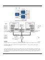
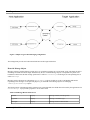
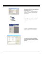
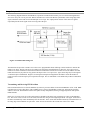
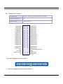
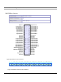
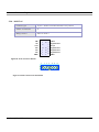
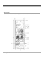
1
Conejo User's Manual
Conejo User's Manual
The Conejo User's Manual was prepared by the technical staff of
Innovative Integration on February 5, 2009.
For further assistance contact:
Innovative Integration
2390-A Ward Ave
Simi Valley, California 93065
PH:
FAX:
(805) 578-4260
(805) 578-4225
email: [email protected]
Website: www.innovative-dsp.com
This document is copyright 2009 by Innovative Integration. All rights
are reserved.
VSS \ Distributions \ Conejo \ Documentation \ Manual \
ConejoMaster.odm
#XXXXXX
Rev 1.0
Table of Contents
Chapter 1. Introduction..........................................................................................................................13
Real Time Solutions!.............................................................................................................................................................13
Vocabulary.............................................................................................................................................................................13
What is Matador? ......................................................................................................................................................14
What is Conejo? ........................................................................................................................................................15
What is Malibu? ........................................................................................................................................................15
What is C++ Builder?.................................................................................................................................................15
What is Microsoft MSVC?.........................................................................................................................................15
What kinds of applications are possible with Innovative Integration hardware?.......................................................15
Why do I need to use Malibu with my Baseboard?....................................................................................................15
Finding detailed information on Malibu.....................................................................................................................16
Online Help......................................................................................................................................................................16
Innovative Integration Technical Support........................................................................................................................16
Innovative Integration Web Site......................................................................................................................................16
Typographic Conventions......................................................................................................................................................17
Chapter 2. Baseboard Overview............................................................................................................18
The Innovative Baseboard Family.........................................................................................................................................18
Analog Digital Inverting Outputs.....................................................................................................................................18
The Baseboard Device Driver..........................................................................................................................................19
Multiple Baseboards.........................................................................................................................................................19
Slave Accesses.................................................................................................................................................................20
Data Transfers..................................................................................................................................................................20
Class Libraries..................................................................................................................................................................22
Malibu.........................................................................................................................................................................22
Chapter 3. A Tour of Malibu.................................................................................................................23
Class Groups In Malibu.........................................................................................................................................................23
Utility Classes..................................................................................................................................................................24
Events and Event Handlers.........................................................................................................................................25
Windows Synchronization..........................................................................................................................................25
Thread Classes............................................................................................................................................................25
Multi-threading Utility Classes..................................................................................................................................25
Buffer and Message Classes.......................................................................................................................................26
Disk I/O Classes.........................................................................................................................................................26
Hardware Support Classes...............................................................................................................................................27
Subsystem Interfaces..................................................................................................................................................27
Target I/O Streaming Classes.....................................................................................................................................27
Analysis Classes...............................................................................................................................................................28
Vector (1D) Signal Processing Components..............................................................................................................28
Data Storage and Retrieval.........................................................................................................................................29
Conversion Functions.................................................................................................................................................29
PCI Board Support Classes..............................................................................................................................................30
Baseboards and PMC Modules..................................................................................................................................30
Using the Malibu Component Suite.......................................................................................................................................31
Creating a Streaming Application in Visual C++............................................................................................................31
Creating the Malibu Objects.......................................................................................................................................31
Conejo User's Manual
3
Initializing Object Properties and Events...................................................................................................................33
Event Handler Code...................................................................................................................................................33
Loading COFF Files...................................................................................................................................................35
Loading Logic Files....................................................................................................................................................36
Script Files..................................................................................................................................................................36
Chapter 4. About the Baseboard...........................................................................................................38
Velocia Family Overview......................................................................................................................................................38
Quadia Overview.............................................................................................................................................................38
Processing Cluster............................................................................................................................................................39
Connectivity.....................................................................................................................................................................40
PCI Buses...................................................................................................................................................................40
Data Plane...................................................................................................................................................................41
Global Memory Pool........................................................................................................................................................42
Timing and Synchronization Features.............................................................................................................................42
The Pismo Class Library........................................................................................................................................................43
Simple To Use............................................................................................................................................................43
Not Just for C++ Experts ...........................................................................................................................................44
Unique Feature Support for each Baseboard..............................................................................................................44
Digital Signal Processor.........................................................................................................................................................44
DSP External Memory.....................................................................................................................................................44
DSP Initialization.............................................................................................................................................................44
DSP JTAG Debugger Support.........................................................................................................................................47
FPGA JTAG Support.......................................................................................................................................................47
Using the Malibu Baseboard Components............................................................................................................................48
PCI Interrupt Configuration and Compatibility...............................................................................................................49
DSP Programming on the Baseboard....................................................................................................................................49
Device Drivers.................................................................................................................................................................50
Advantages of using DSP/BIOS drivers.....................................................................................................................50
How to use a DSP/BIOS driver..................................................................................................................................50
Driver-specific control functions................................................................................................................................52
Driver Buffer Model...................................................................................................................................................52
Driver Types...............................................................................................................................................................53
Driver Implementation...............................................................................................................................................53
DMA-enabled Drivers................................................................................................................................................54
Simplified Use............................................................................................................................................................54
Multitasking Friendly.................................................................................................................................................55
Analog Timebase Objects................................................................................................................................................55
Timebase Usage..........................................................................................................................................................55
Interrupt Handling............................................................................................................................................................56
Interrupts in a C++ Environment................................................................................................................................56
The Pismo Solution....................................................................................................................................................56
Class Irq......................................................................................................................................................................57
Interrupt Lock Classes................................................................................................................................................57
Interrupt Binder Templates .............................................................................................................................................58
Class InterruptHandler................................................................................................................................................58
Class ClassMemberHandler Template.......................................................................................................................58
Class FunctionHandler Template...............................................................................................................................59
EDMA and QDMA Handling..........................................................................................................................................59
Class DmaSettings......................................................................................................................................................60
Class Qdma.................................................................................................................................................................60
Conejo User's Manual
4
Class Edma.................................................................................................................................................................61
Linked and Chained blocks........................................................................................................................................63
Class EdmaMaster......................................................................................................................................................64
Chapter 5. Host/Target Communications.............................................................................................65
Overview..........................................................................................................................................................................65
CPU Busmastering Interface.................................................................................................................................................66
CPU Busmastering Implementation.................................................................................................................................66
Packet Based Transfers...............................................................................................................................................66
Blocking Interface......................................................................................................................................................66
Maximum Transfer Size.............................................................................................................................................66
Host (Malibu Library) Support for CPU Busmastering...................................................................................................67
Target (Pismo Library) Support for CPU Busmastering..................................................................................................67
Packetized Message Interface................................................................................................................................................68
Message Mailboxes..........................................................................................................................................................68
The Message System........................................................................................................................................................68
Host-side Message Objects..............................................................................................................................................69
Target Side Message Objects...........................................................................................................................................70
Message Communication.................................................................................................................................................71
C++ Terminal I/O..................................................................................................................................................................72
Target Software................................................................................................................................................................72
Tutorial.............................................................................................................................................................................72
Chapter 6. Windows Installation...........................................................................................................74
Host Hardware Requirements................................................................................................................................................74
Software Installation..............................................................................................................................................................74
Starting the Installation ...................................................................................................................................................75
The Installer Program.......................................................................................................................................................76
Tools Registration..................................................................................................................................................................78
Bus Master Memory Reservation Applet...................................................................................................................78
Hardware Installation.............................................................................................................................................................79
After Power-up......................................................................................................................................................................80
Chapter 7. JTAG Hardware Installation..............................................................................................81
JTAG Emulator Hardware Installation (for DSP boards Only).............................................................................................81
PCI Pod-Based Emulator Installation....................................................................................................................................81
Baseboard Installation............................................................................................................................................................82
A Few Considerations BEFORE Power-up...........................................................................................................................82
It cannot be overemphasized: ....................................................................................................................................82
After Power-up...........................................................................................................................................................83
Code Composer Studio Setup with II Jtag.............................................................................................................................83
Setting up for a single processor with Spectrum Digital USB Jtag.......................................................................................87
Setting up for Multi Processors with Spectrum Digital USB Jtag.........................................................................................90
Borland Builder Setup and Use.............................................................................................................................................93
Automatic saving of project files and forms during debugging.................................................................................93
Static-binding of built executables. ...........................................................................................................................94
Appropriate library and include paths. .....................................................................................................................94
Chapter 8. Building a Target DSP Project...........................................................................................96
Writing a Program...............................................................................................................................................................101
Host Tools for Target Application Development................................................................................................................101
Conejo User's Manual
5
Components of Target Code (.cpp, .tcf, .cmd, .pjt).......................................................................................................101
Edit-Compile-Test Cycle using Code Composer Studio.....................................................................................................102
Automatic projectfile creation........................................................................................................................................102
Rebuilding a Project.......................................................................................................................................................102
IIMain replaces main................................................................................................................................................102
Running the Target Executable......................................................................................................................................102
Note:.........................................................................................................................................................................103
Anatomy of a Target Program.............................................................................................................................................103
Use of Library Code.......................................................................................................................................................104
Example Programs...............................................................................................................................................................104
The Next Step: Developing Custom Code...........................................................................................................................105
Chapter 9. Conejo Input and Output..................................................................................................106
Analog Inputs.......................................................................................................................................................................106
Overview........................................................................................................................................................................106
A/D Anti-alias Filtering and Input Circuitry..................................................................................................................107
A/D Triggering and Data Collection..............................................................................................................................110
Enabling the data acquisition engine..............................................................................................................................110
Data Format....................................................................................................................................................................110
A/D Error Correction.....................................................................................................................................................111
A/D Calibration..............................................................................................................................................................112
A/D Data Latency and Decimation Mode......................................................................................................................112
A/D Data Flow Controls and Data Buffering................................................................................................................113
Monitoring A/D Data Flow Errors.................................................................................................................................114
Analog Input Timebases and Triggering........................................................................................................................114
Software Support............................................................................................................................................................115
Hardware Support..........................................................................................................................................................118
A/D Frame Timer...........................................................................................................................................................122
Analog Outputs....................................................................................................................................................................123
Smoothing Filter Characteristics....................................................................................................................................125
D/A Triggering and Data Collection..............................................................................................................................127
Enabling The D/A data conversion engine....................................................................................................................127
D/A Data Format............................................................................................................................................................127
D/A Error Correction.....................................................................................................................................................128
D/A Calibration..............................................................................................................................................................129
D/A Data Flow Controls and Data Buffering................................................................................................................129
Monitoring D/A Data Flow Errors.................................................................................................................................130
Analog Output Timebases and Triggering.....................................................................................................................131
Software Support............................................................................................................................................................131
Timebase Software Objects. ....................................................................................................................................133
Hardware Support..........................................................................................................................................................135
D/A Clock Sources. .................................................................................................................................................135
Timebase for Servo Applications. ...........................................................................................................................136
Start and Stop Triggers. ...........................................................................................................................................137
D/A Frame Timer. ...................................................................................................................................................139
D/A Frame Counter. ................................................................................................................................................140
Single-Shot Mode. ..................................................................................................................................................140
Chapter 10. Target Peripheral Devices...............................................................................................141
DSP Interrupts......................................................................................................................................................................141
Software Support............................................................................................................................................................141
Conejo User's Manual
6
Hardware Implementation..............................................................................................................................................141
Conditioning for Interrupt Input Signals........................................................................................................................142
Shared/ Dedicated Interrupts..........................................................................................................................................143
External User Interrupt Usage........................................................................................................................................144
Digital I/O............................................................................................................................................................................144
Software Support............................................................................................................................................................144
Hardware Implementation..............................................................................................................................................145
Digital I/O Timing..........................................................................................................................................................146
Digital IO Electrical Characteristics..............................................................................................................................147
Timers..................................................................................................................................................................................147
Software Support............................................................................................................................................................147
Hardware Implementation..............................................................................................................................................148
On-chip Timers. .......................................................................................................................................................148
AD9851 Direct Digital Synthesizer. ........................................................................................................................148
Counters...............................................................................................................................................................................149
Software Support............................................................................................................................................................149
Hardware Implementation..............................................................................................................................................150
SyncLink and ClockLink.....................................................................................................................................................151
Software Support............................................................................................................................................................151
Hardware Implementation..............................................................................................................................................151
Alert Log..............................................................................................................................................................................152
Overview........................................................................................................................................................................152
Software Support............................................................................................................................................................153
Alert Objects. ...........................................................................................................................................................154
Alert Binder Templates. ..........................................................................................................................................154
Using Alerts in Application Code. ..........................................................................................................................154
Host Side Support. ...................................................................................................................................................155
Hardware Implementation..............................................................................................................................................155
Alert Log Message Format.............................................................................................................................................156
Controlling and Monitoring the Alert Log.....................................................................................................................157
Alert Log Data Flow......................................................................................................................................................157
Serial EEPROM Interface....................................................................................................................................................158
FIFOPort I/O Expansion......................................................................................................................................................158
Software Support............................................................................................................................................................158
FifoportIn. ................................................................................................................................................................158
FifoPortOut. .............................................................................................................................................................159
Basic Fifoport Access. .............................................................................................................................................159
Hardware Implementation..............................................................................................................................................159
Transmitting and Receiving FIFOPort Data..................................................................................................................160
Monitoring FIFO Status.................................................................................................................................................161
FIFOPort Reset...............................................................................................................................................................162
Controlling the FIFOPort Programmable Level Flag....................................................................................................162
Designing External Hardware for use with the FIFOPort..............................................................................................163
Chapter 11. Developing Custom Data Logger Applications.............................................................166
ASnap Example...................................................................................................................................................................166
Tools Required...............................................................................................................................................................166
Partitioning.....................................................................................................................................................................167
Design Goals........................................................................................................................................................................167
Download.......................................................................................................................................................................168
Setup...............................................................................................................................................................................168
Conejo User's Manual
7
Logging. ...................................................................................................................................................................169
Channel Enable. ......................................................................................................................................................170
Channel-Specific Programmable Gain. ..................................................................................................................170
Timebase and Triggering Options. .........................................................................................................................172
Target Application...............................................................................................................................................................176
Streaming Acquisition.........................................................................................................................................................178
Summary..............................................................................................................................................................................182
Chapter 12. Streaming Mode Operation............................................................................................183
Malibu Configuration..........................................................................................................................................................183
Preliminary Requirements..............................................................................................................................................183
Stream Interrupt Sources................................................................................................................................................184
Target-Initiated Streaming........................................................................................................................................184
Block-Mode Streaming........................................................................................................................................................184
Implementing Application-Specific Filters.........................................................................................................................185
The GenericFloat Filter........................................................................................................................................................185
OnStart. ....................................................................................................................................................................185
OnStop. ....................................................................................................................................................................185
OnData. ....................................................................................................................................................................185
GenericRaw Filter................................................................................................................................................................186
Sample Application Code:...................................................................................................................................................186
Chapter 13. Servo Applications...........................................................................................................189
Data Acquisition Applications.................................................................................................................................189
Servoing Applications. ............................................................................................................................................189
Servoing and DSP/BIOS. ........................................................................................................................................189
The Servo Base Class. .............................................................................................................................................189
Using the Servo Class..........................................................................................................................................................190
Servo Interrupt Modes....................................................................................................................................................190
ProcessEvent()................................................................................................................................................................191
Timebases.......................................................................................................................................................................191
DAC Delay. .............................................................................................................................................................191
Channel Selection...........................................................................................................................................................191
Servo Timing.......................................................................................................................................................................191
A Servo Tutorial..................................................................................................................................................................192
Configuring the CDB.....................................................................................................................................................195
Conclusion......................................................................................................................................................................196
Chapter 14. Developing Host Applications.........................................................................................197
Borland Turbo C++..............................................................................................................................................................197
Other considerations:.....................................................................................................................................................198
Microsoft Visual Studio 2005..............................................................................................................................................199
DialogBlocks.......................................................................................................................................................................201
Summary..............................................................................................................................................................................201
Chapter 15. Applets..............................................................................................................................202
Common Applets.................................................................................................................................................................202
Registration Utility (NewUser.exe)...............................................................................................................................202
Reserve Memory Applet (ReserveMemDsp.exe).........................................................................................................203
Data Analysis Applets.........................................................................................................................................................203
Binary File Viewer Utility (BinView.exe).....................................................................................................................203
Conejo User's Manual
8
Target Programming Applets...............................................................................................................................................204
Target Project Copy Utility (CopyCcsProject.exe)........................................................................................................204
Demangle Utility (Demangle.exe).................................................................................................................................204
COFF Section Dump Utility (CoffDump.exe)...............................................................................................................204
JTAG Diagnostic Utility (JtagDiag.exe)........................................................................................................................205
RtdxTerminal - Terminal Emulator...............................................................................................................................205
Important Note:........................................................................................................................................................205
Terminal Emulator Menu Commands......................................................................................................................205
The File Menu..........................................................................................................................................................206
The DSP Menu.........................................................................................................................................................206
The Form Menu........................................................................................................................................................207
The Help Menu.........................................................................................................................................................207
Options Tab:.............................................................................................................................................................207
Display Group..........................................................................................................................................................208
Sounds Group...........................................................................................................................................................209
Coff Load Group......................................................................................................................................................209
Debugger Group.......................................................................................................................................................209
Terminal Emulator Command Line Switches..........................................................................................................210
Applets for the Matador Baseboards...................................................................................................................................210
Board Finder (MatadorFinder.exe)................................................................................................................................210
Logic Update Utility (MatadorVsProm5.exe/VelociaVsProm.exe)..............................................................................211
Target Download Utility (MatadorDownload.exe)........................................................................................................211
Chapter 16. Connector Pinout and Physical Information................................................................212
Conejo Connector Pinouts...................................................................................................................................................212
Analog Input/Output Connectors...................................................................................................................................212
J1 – External Clock Input...............................................................................................................................................213
J2 – External Interrupt Input..........................................................................................................................................214
JP1 – Digital I/O Connector...........................................................................................................................................215
JP3 – UD Digital I/O Connector....................................................................................................................................216
JP4 -FIFOPort Connector...............................................................................................................................................217
JP8 – SyncLink/ClockLink............................................................................................................................................218
JP11 – DSP JTAG..........................................................................................................................................................219
Board Layout.......................................................................................................................................................................221
Chapter 17. Troubleshooting...............................................................................................................222
Initialization Problems.........................................................................................................................................................223
The system does not recognize my board(s)..................................................................................................................223
I created an EXE file and when I try to run it, the system requires a DLL which I don’t have.....................................223
What DLLs do I have to deploy with my newly created executable?...........................................................................224
How do I know what DLLs my executable is dependent on?........................................................................................224
DSP Hardware Problems.....................................................................................................................................................224
The I/O seems like it is not connected or doesn’t work.................................................................................................224
How can I tell what version of logic I am using?..........................................................................................................225
Quadia Hardware Problems................................................................................................................................................225
How do I update the logic?............................................................................................................................................225
I updated the logic, but it did not work..........................................................................................................................225
Conejo User's Manual
9
List of Tables
Table 1. Quixote ‘C6416 DSP EMIF Control Register Initialization Values.......................................................................45
Table 2. Quadia ‘C6416 DSP EMIF Control Register Initialization Values.........................................................................46
Table 3. Velocia Baseboard Components..............................................................................................................................48
Table 4. Velocia Family Baseboard Logic Configuration Methods......................................................................................48
Table 5. Velocia Family Baseboard COFF Loading Methods..............................................................................................49
Table 6. Timebase Operations...............................................................................................................................................56
Table 7. Interrupt Lock Classes.............................................................................................................................................58
Table 8. TIIMessage Header Field Access............................................................................................................................69
Table 9. MatadorMessage Data Section Interface................................................................................................................70
Table 10. IIMessage Header Field Access.............................................................................................................................70
Table 11. TIIMessage Data Section Interface......................................................................................................................71
Table 12. TIIMessage Data Section Interface......................................................................................................................71
Table 13. Pismo Example Programs....................................................................................................................................105
Table 14. Timebase Operation Modes.................................................................................................................................116
Table 15. Analog In Timebase Object Types......................................................................................................................117
Table 16. D/A Maximum Update Rates..............................................................................................................................124
Table 17. Timebase Operation Modes................................................................................................................................133
Table 18. Analog In Timebase Object Types......................................................................................................................134
Table 19. DigitalIo Class Operations...................................................................................................................................144
Table 20. Digital I/O Port Timing Parameters.....................................................................................................................146
Table 21. Timer Management Objects................................................................................................................................147
Table 22. Counter Management Objects.............................................................................................................................149
Table 23. FIFO Port Timing Parameters.............................................................................................................................164
Table 24. Development Tools Used to Build ASnap Project..............................................................................................166
Table 25. The Servo Class Virtual Function........................................................................................................................190
Table 26. Servo Time Measurements..................................................................................................................................191
Table 27. Windows driver files............................................................................................................................................223
Conejo User's Manual
10
List of Figures
Figure 1. Bus-mastering efficiently transfers data between target and host memory............................................................21
Figure 2. Bus mastering transfers are always initiated by the Host libraries when controlling Velocia PMC modules.......22
Figure 3. Quadia Processing Cluster Block Diagram............................................................................................................40
Figure 4. Quadia Data Plane Connections.............................................................................................................................41
Figure 5. Quadia DSP JTAG Chain.......................................................................................................................................47
Figure 6. Quadia FPGA JTAG Chain....................................................................................................................................47
Figure 7. Simple Target to Host Messaging configuration....................................................................................................69
Figure 8. Vista Verificaton Dialog........................................................................................................................................75
Figure 9. Innovative Install Program....................................................................................................................................76
Figure 10. Progress is shown for each section.......................................................................................................................77
Figure 11. ToolSet registration form.....................................................................................................................................78
Figure 12. BusMaster configuration......................................................................................................................................78
Figure 13. Installation complete............................................................................................................................................79
Figure 14. Interconnections of the Analog Input Sub-System.............................................................................................107
Figure 15. Gain and offset settings for input ranges............................................................................................................107
Figure 16. A/D anti-alias filter frequency response.............................................................................................................109
Figure 17. Multiple A/D channel ordering and data set format...........................................................................................110
Figure 18. Single A/D channel format in special stacked mode format..............................................................................111
Figure 19. Calibration memory locations............................................................................................................................111
Figure 20. A/D Channel Enable Register (0x80210000).....................................................................................................113
Figure 21. A/D FIFO Level and Status Register (0x803D0000).........................................................................................113
Figure 22. A/D FIFO Interrupt Threshold Level Register (0x80220000............................................................................114
Figure 23. A/D triggering fundamentals..............................................................................................................................115
Figure 24. A/D conversion timebase (0x80130000)............................................................................................................118
Figure 25. A/D start trigger selection register (0x80280000)..............................................................................................119
Figure 26. A/D stop trigger selection register (0x80280008)..............................................................................................120
Figure 27. A/D Trigger polarity and type selection register (start = 0x80280004, stop = 0x8028000C)...........................121
Figure 28. Threshold Channel and Hysteresis Register (0x80280014)...............................................................................121
Figure 29. Threshold value register (0x80280010).............................................................................................................121
Figure 30. Threshold trigger example with programmable hysteresis of 4 samples...........................................................122
Figure 31. A/D Frame Timer Register (0x80280018).........................................................................................................122
Figure 32. A/D Frame Counter Register (0x8028001C).....................................................................................................123
Figure 33. D/A Channel Circuitry.......................................................................................................................................125
Figure 34. DAC smoothing filter frequency response.........................................................................................................126
Figure 35. Detail of the DAC smoothing filter frequency response....................................................................................126
Figure 36. D/A channel ordering and data set format for multiple channels.......................................................................127
Figure 37. D/A channel ordering and data set format for DAC 0 used in single channel mode.........................................128
Figure 38. D/A calibration memory addresses....................................................................................................................129
Figure 39. D/A Channel Enable Register (0x80250000).....................................................................................................129
Figure 40. D/A FIFO Level and Status Register (0x803C0000).........................................................................................129
Figure 41. D/A FIFO Interrupt Threshold Level Register (0x80260000)...........................................................................130
Figure 42. DAC triggering Fundamentals...........................................................................................................................131
Figure 43. D/A conversion timebase (0x80130000)............................................................................................................135
Figure 44. D/A Timebase Delay Register (0x80290010)....................................................................................................136
Figure 45. Programmable Delay Timing Diagram..............................................................................................................137
Figure 46. D/A start trigger selection register (0x80290000)..............................................................................................138
Figure 47. D/A stop trigger selection register (0x80290008)..............................................................................................138
Conejo User's Manual
11
Figure 48. D/A Trigger Selection Logic..............................................................................................................................139
Figure 49. D/A Trigger polarity and type selection register (start = 0x80290004, stop = 0x8029000C)...........................139
Figure 50. D/A Frame Timer Register (0x80290018).........................................................................................................139
Figure 51. D/A Frame Counter Register (0x8029001C).....................................................................................................140
Figure 52. External Interrupt Input Control Register Addresses.........................................................................................141
Figure 53. External Interrupt Input Control Register Definitions.......................................................................................142
Figure 54. Interrupt polarity and type selection (polarity = 0x80110000, type = 0x80100000).........................................143
Figure 55. External Interrupt Status and Acknowledge Register Addresses.......................................................................143
Figure 56. DIO Control Register (0x80000000)..................................................................................................................145
Figure 57. UD Digital I/O Configuration Control Register (0x802A0000)........................................................................145
Figure 58. UD Digital I/O Configuration Control Register Definition (0x802A0000).......................................................145
Figure 59. Digital IO Port Addresses...................................................................................................................................146
Figure 60. Digital I/O Port Timing......................................................................................................................................146
Figure 61. DSP On-chip Timer Clock Source Control Register (0x80140000)..................................................................148
Figure 62. DDS Control Register (0x80020000).................................................................................................................149
Figure 63. Counter Configuration Registers (Counter 0 = 0x80330000, Counter 1 =0x80340000, Counter 2 =
0x80350000)........................................................................................................................................................................150
Figure 64. Counter Registers (Counter 0 = 0x80330000, Counter 1 = 0x80340000, Counter 2 =0x80350000)................150
Figure 65. External Timer/Counter Period Formulas..........................................................................................................150
Figure 66. SyncLink/ClockLink Control Register Definition (0x80120000)......................................................................151
Figure 67. SyncLink Signals (when master)........................................................................................................................152
Figure 68. Alert Log Enables Register (0x80230000).........................................................................................................156
Figure 69. Alert Message Format (0x803F0000)................................................................................................................156
Figure 70. Alert Log Event Types.......................................................................................................................................157
Figure 71. FIFOPort Block Diagram...................................................................................................................................160
Figure 72. FIFOPort Status Register (0x801C0000 read-only)...........................................................................................161
Figure 73. FIFOPort Control Register (0x801C0000, write-only)......................................................................................161
Figure 74. FIFO Port Timing...............................................................................................................................................164
Figure 75. DownloadTarget Function..................................................................................................................................168
Figure 76. ASnap GenericEvent Handler............................................................................................................................175
Figure 77. DSP Mailbox Message Processing in ASnap....................................................................................................176
Figure 78. Target Initialization Sequence............................................................................................................................177
Figure 79. Target Streaming................................................................................................................................................179
Figure 80. Sample OnFilterData Handler............................................................................................................................186
Figure 81. RtdxTerminal Options........................................................................................................................................208
Figure 82. Digital I/O Connector Pinout.............................................................................................................................215
Figure 83. Digital I/O Connector Pin Orientation...............................................................................................................215
Figure 84. UD Digital I/O Connector Pinout.......................................................................................................................216
Figure 85. UD Digital I/O Connector Pin Orientation.........................................................................................................216
Figure 86. FIFOPort Connector Pinout................................................................................................................................217
Figure 87. FIFOPort Connector Pin Orientation.................................................................................................................217
Figure 88. SyncLink/ClockLink Connector Pinouts............................................................................................................218
Figure 89. SyncLink/ClockLink Connector Pin Orientation...............................................................................................218
Figure 90. JTAG Connector Pinouts....................................................................................................................................219
Figure 91. JTAG Connector Pin Orientation.......................................................................................................................219
Conejo User's Manual
12
Introduction
Chapter 1.
Introduction
Real Time Solutions!
Thank you for choosing Innovative Integration, we appreciate your business! Since 1988, Innovative Integration has grown
to become one of the world's leading suppliers of DSP and data acquisition solutions. Innovative offers a product portfolio
unrivaled in its depth and its range of performance and I/O capabilities .
Whether you are seeking a simple DSP development platform or a complex, multiprocessor, multichannel data acquisition
system, Innovative Integration has the solution. To enhance your productivity, our hardware products are supported by
comprehensive software libraries and device drivers providing optimal performance and maximum portability.
Innovative Integration's products employ the latest digital signal processor technology thereby providing you the competitive
edge so critical in today's global markets. Using our powerful data acquisition and DSP products allows you to incorporate
leading-edge technology into your system without the risk normally associated with advanced product development. Your
efforts are channeled into the area you know best ... your application.
Vocabulary
Conejo User's Manual
13
Introduction
What is Matador?
Matador is Innovative Integration’s new baseboard architecture that integrates a board-specific, high-performance analog,
video or digital peripheral “front-end” with a high-performance DSP and peripheral core . Each baseboard includes an
onboard TMS320C671x DSP with 32 MB cached SDRAM which accesses to the entire baseboard peripheral complement
directly as memory mapped devices. Each baseboard supports a 64-bit, streaming, bus-mastering PCI bus interface, sixteen
general purpose 32-bit mailboxes, dedicated FifoPort and SyncLink buses for inter-board connectivity, a precision DDS
timebase to serve as an accurate, programmable clock source from DC-25 MHz and a programmable digital I/O port.
Because of the onboard DSP, each Matador is capable of performing data collection, servo or other real-time processing and
data movement automatically without Host CPU involvement.
Conejo User's Manual
14
Introduction
What is Conejo?
Conejo is Innovative Integration’s Matador-family baseboard that provides a hardware front-end of up to 4 simultaneous
channels of independent A/D operating at 14-bit, DC-10 MHz, and D/A conversion at 16 bits operating from DC-50
MHz(single channel) or 15 MHz for four simultaneous channels. Applications include ultrasound, communications, high
speed controls.
What is Malibu?
Malibu is the Innovative Integration-authored component suite, which combines with the Borland, Microsoft or GNU C++
compilers and IDEs to support programming of Innovative hardware products under Windows and Linux. Malibu supports
both high-speed data streaming plus asynchronous mailbox communications between the DSP and the Host PC, plus a wealth
of Host functions to visualize and post-process data received from or to be sent to the target DSP.
What is C++ Builder?
C++ Builder is a general-purpose code-authoring environment suitable for development of Windows applications of any type.
Armada extends the Builder IDE through the addition of functional blocks (VCL components) specifically tailored to
perform real-time data streaming functions.
What is Microsoft MSVC?
MSVC is a general-purpose code-authoring environment suitable for development of Windows applications of any type.
Armada extends the MSVC IDE through the addition of dynamically created MSVC-compatible C++ classes specifically
tailored to perform real-time data streaming functions.
What kinds of applications are possible with Innovative Integration hardware?
Data acquisition, data logging, stimulus-response and signal processing jobs are easily solved with Innovative Integration
baseboards using the Malibu software. There are a wide selection of peripheral devices available in the Matador DSP
product family, for all types of signals from DC to RF frequency applications, video or audio processing. Additionally,
multiple Innovative Integration baseboards can be used for a large channel or mixed requirement systems and data
acquisition cards from Innovative can be integrated with Innovative's other DSP or data acquisition baseboards for highperformance signal processing.
Why do I need to use Malibu with my Baseboard?
One of the biggest issues in using the personal computer for data collection, control, and communications applications is the
relatively poor real-time performance associated with the system. Despite the high computational power of the PC, it cannot
reliably respond to real-time events at rates much faster than a few hundred hertz. The PC is really best at processing data,
not collecting it. In fact, most modern operating systems like Windows are simply not focused on real-time performance, but
rather on ease of use and convenience. Word processing and spreadsheets are simply not high-performance real-time tasks.
Conejo User's Manual
15
Introduction
The solution to this problem is to provide specialized hardware assistance responsible solely for real- time tasks. Much the
same as a dedicated video subsystem is required for adequate display performance, dedicated hardware for real-time data
collection and signal processing is needed. This is precisely the focus of our baseboards – a high performance, state-of-theart, dedicated digital signal processor coupled with real-time data I/O capable of flowing data via a 64-bit PCI bus interface.
The hardware is really only half the story. The other half is the Malibu software tool set which uses state of the art software
techniques to bring our baseboards to life in the Windows environment. These software tools allow you to create applications
for your baseboard that encompass the whole job - from high speed data acquisition, to the user interface.
Finding detailed information on Malibu
Information on Malibu is available in a variety of forms:
•
Data Sheet (http://www.innovative-dsp.com/products/malibu.htm)
•
On-line Help
•
Innovative Integration Technical Support
•
Innovative Integration Web Site (www.innovative-dsp.com)
Online Help
Help for Malibu is provided in a single file, Malibu.chm which is installed in the Innovative\Documentation folder during the
default installation. It provides detailed information about the components contained in Malibu - their Properties, Methods,
Events, and usage examples. An equivalent version of this help file in HTML help format is also available online at
http://www.innovative-dsp.com/support/onlinehelp/Malibu.
Innovative Integration Technical Support
Innovative includes a variety of technical support facilities as part of the Malibu toolset. Telephone hotline supported is
available via
Hotline (805) 578-4260 8:00AM-5:00 PM PST.
Alternately, you may e-mail your technical questions at any time to:
[email protected].
Also, feel free to register and browse our product forums at http://forum.iidsp.com/, which are an excellent source of FAQs
and information submitted by Innovative employees and customers.
Innovative Integration Web Site
Additional information on Innovative Integration hardware and the Malibu Toolset is available via the Innovative Integration
website at www.innovative-dsp.com
Conejo User's Manual
16
Introduction
Typographic Conventions
This manual uses the typefaces described below to indicate special text.
Typeface
Source Listing
Boldface
Emphasis
Cpp Variable
Cpp Symbol
KEYCAPS
Menu Command
Conejo User's Manual
Meaning
Text in this style represents text as it appears onscreen or in code. It
also represents anything you must type.
Text in this style is used to strongly emphasize certain words.
Text in this style is used to emphasize certain words, such as new
terms.
Text in this style represents C++ variables
Text in this style represents C++ identifiers, such as class, function,
or type names.
Text in this style indicates a key on your keyboard. For example,
“Press ESC to exit a menu”.
Text in this style represents menu commands. For example “Click
View | Tools | Customize”
17
Baseboard Overview
Chapter 2.
Baseboard Overview
Before discussing the details of software development, a basic understanding of the components of the Malibu system and
their relationships to the hardware are required. This chapter provides the “big picture” view and additional information that
will make the details provided in the later chapters more clear.
The Innovative Baseboard Family
Innovative family baseboards are a synergistic blend of digital signal processor hardware and data acquisition hardware.
These baseboards provide a fast, flexible signal processing and data movement hardware platform with features far ahead of
the competition.
Velocia and Matador family baseboard features include:
•
A 32/64-bit, 33/66 Mhz, PCI/cPCI/PMC bus host interface with direct host memory access capability for busmastering data between the card and host memory. The interface also supports PCI slave mode accesses from the
host for logic configuration and application downloading.
If the board is processor-equipped, the baseboard’s features include:
•
One or more onboard, dedicated DSP(s) for off-loading I/O processing from the host to allow data acquisition and
signal processing at maximum rates. Members of the Innovative family utilize an advanced TI TMS320C6416 DSP
with up to 64 MB SDRAM, enhanced cache controller, sixty-four DMA channels, three MCBSP sync serial ports
and two 32-bit counter/timers. The DSP runs the royalty-free, multitasking, real-time operating system - DSP/BIOS.
Analog Digital Inverting Outputs
ADCs may have inverted output stages on the target device. If ADCs are inverted, a positive voltage will yield a negative
value in the capture buffer, and a negative voltage will yield a positive value. DACs may also have inverted output stages in
that a negative value will produce a positive voltage, and a positive value will produce a negative voltage.
The following table illustrates the inverting qualities for each product:
Conejo User's Manual
18
Baseboard Overview
Product
ADC
DAC
Conejo
Inverted
non-Inverted
Delfin
Inverted
non-Inverted
Oruga
non-Inverted
Inverted
Toro
Inverted
Inverted
The Baseboard Device Driver
Innovative baseboards are Plug-and-Play PCI devices which require a device driver for Win2K and WinXP. The same device
driver, iixwdm.sys, is used for all PCI -equipped baseboards. The appropriate driver is installed as part of the normal
installation process for each baseboard. The driver accepts the resource assignments given for the board and configures the
software to use them, making the board fully recognized by Windows.
The device driver also reserves a block of contiguous, physical memory for use as a region for bus-master transfers. This
block ranges upwards from 2 MB in size. A separate region is required for each DSP on each baseboard and this is
permanently reserved for use by that DSP; it will not be available for Windows applications or other boards.
Under Win2k and WinXP, reserving this space may require the raising of the reserved system memory ceiling whenever:
1.
One or more baseboards are installed into the PC system (including initial installation!)
2.
Operating at high data acquisition rates or with large channel-count systems
An applet, ReserveMemDsp.exe, is provided to support manual adjustment of these registry properties. It must be run
prior to attempting to use the DSP, run any of the supplied examples, etc. See the Applets chapter for details.
Multiple Baseboards
When installing more than one baseboard in a system, a means of uniquely addressing each installed baseboard must be
employed. Windows automatically loads the baseboard device driver for each board as it initializes after PC boot-up. During
this cold-start initialization, a unique instance of strategic portions of the device driver is allocated for each board installed in
the PC. Correspondingly, each base board is assigned an integer identifier, referred to as the target number, which
corresponds to the baseboard’s place in the driver allocation sequence. These target numbers are assigned based on the
placement of the boards on the PCI bus, so the assignment for a particular arrangement of boards is fixed unless boards are
removed or re-arranged. If additional boards are added, target assignments for all boards may change.
Unfortunately, the relationship between PCI slots and driver-assigned target numbers is system-dependent. So, a means of
associating a target number with a baseboard installed in a particular PCI slot is needed. To determine the slot-to-targetnumber associations, each Innovative baseboard has an LED that can be illuminated by a software access from the host. The
Conejo User's Manual
19
Baseboard Overview
included troubleshooting applet, Finder.exe, can be used to activate the LED for a specific target to determine the proper
target assignments. See the Applets chapter for details.
Slave Accesses
All baseboard and user logic peripherals can be accessed from the Host CPU using PCI slave-mode accesses. In this mode,
the Host CPU can perform 32-bit fetches or stores to any decoded memory region in the target address space to obtain or
change their current value using the device's dedicated PCI bus interface. Since all target peripherals are memory-mapped,
this allows the Host CPU to read or write any target peripheral register or memory location.
Despite their flexibility, slave accesses are unsuitable for applications requiring high-speed data transfer between the host and
target. Firstly, slave accesses are non-deterministic, since they are called by Windows applications which are routinely
preempted. Also, they are intrinsically rate-limited, since they are implemented as individual Host CPU read/write
operations rather than efficient, hardware-driven bulk transfers. Nevertheless, slave accesses are invaluable in downloading
target application code or logic and performing other low-bandwidth, asynchronous I/O.
In the Malibu toolset, the baseboard provides public PeekLogic/PokeLogic and PeekPort/PokePort methods for
slave mode accesses to user logic and PCI logic registers, respectively. In order to use these methods, a detailed knowledge
of peripheral register addresses and bit patterns is necessary. See the hardware documentation for your baseboard for a
detailed memory map of all registers implemented in the stock user and PCI logic devices.
Data Transfers
To address high-bandwidth data transfer applications, the baseboard is capable of high-speed transmission and reception of
data via the PCI bus, using a mechanism called bus-mastering. When bus-mastering, the target DSP, which must be running
a downloaded DSP application, transfers data between target DSP memory and Host PC memory automatically with no host
CPU intervention. Since the Host CPU is not directly involved in data movement in bus-mastering mode, it is much more
efficient and deterministic than slave accesses.
Conejo User's Manual
20
Baseboard Overview
Figure 1. Bus-mastering efficiently transfers data between target and host memory
The bus-mastering interface supports sporadic or continuous acquisition and/or playback from multiple channels,
simultaneously. This facility is used when performing high-bandwidth operations, such as acquiring millions of samples per
second from an A/D input channel on the target baseboard.
Bus-mastering input is logically independent of bus-mastering output. It is possible to acquire data from any number and mix
of input devices at a programmed rate. Simultaneously, data may be streamed out to a variety of output devices at a different
programmed rate. Data flow is fully controlled by use of device drivers called from within the Host application.
Conejo User's Manual
21
Baseboard Overview
Figure 2. Bus mastering transfers are always initiated by the Host libraries when controlling Velocia PMC
modules
During data bus-mastering, data flows between areas of page-locked host memory (specifically allocated to each and every
target) and the dedicated, on-board, FIFOs or random access memory devices. The User FPGA can optionally process data
as it travels between peripherals and the host application, unburdening the Host CPU of signal processing tasks providing
enormous flexibility and yielding extremely high performance.
Class Libraries
Malibu
Malibu is the name given to the collective software suite for controlling baseboards, manipulating data streams and for aiding
in the analysis of data. The details of this suite will be more fully discussed in later chapters. In this section, we will give a
general view of how the software relates to Innovative products.
The Malibu suite shields the user from the nitty-gritty details of responding to asynchronous notifications of stream data and
message reception, stream data requirements and message acknowledgements. Instead, a set of special C++ software class
objects, have been created to model each portion of the system. By employing software objects which model the true physical
layout of the system, we can make a full-featured system more understandable.
To illustrate this, imagine that you are using a C64x DSP board within an application, such as that available on the Quadia or
Quixote baseboards. Malibu contains a software component for the board, Innovative::C64xDsp. This component
compartmentalizes all properties and functions necessary to reset, boot and download code to the DSP. Plus, the component
provides properties to read and write via PCI (for slave I/O) and events (callbacks) to respond to conditions, such as when the
baseboard delivers data to the PC for analysis or display. All of these features are controllable via properties and methods of
this baseboard object. The functionality of other baseboards with different capabilities which are supported by Malibu is
irrelevant since their functionality is isolated into other software objects. There is no need to sift through options that do not
apply to your configuration. Malibu’s object-orientated nature provides this benefit automatically.
Conejo User's Manual
22
A Tour of Malibu
Chapter 3.
A Tour of Malibu
The purpose of this section is to provide an introduction to Malibu and a walk-through of the development process for
applications developed using the Malibu library. It is assumed that MSVC or Borland BCB and Malibu are already installed
and operational. This chapter does not attempt to cover general C++ programming or the use of MSVC or BCB.
Class Groups In Malibu
The classes in the Malibu suite fall into several functional categories. These are implemented within different library files
within Malibu to provide maximum autonomy and keep the grouping clear. These categories are outlined in the table and the
following paragraphs.
Category
Purpose
Analysis
Provide access to the common signal processing functions such as filters and FFTs; Logging
and playback of waveforms and other classes needed in data acquisition and control
applications.
Implemented within the Analysis_Mb project.
Utility
Wide variety of common helper classes to manipulate elementary objects such strings,
buffers, threads, semaphores and mutexes; perform file I/O; accurate timing measurements
and delays; implement inter-thread callbacks.
Includes a C++ implementation of OpenWire pins for interconnecting objects to form pump
chains to allow automatic data processing of a data stream. However, all objects also
provide functions that may be used from within the application as a stand-alone operations.
Implemented within the Utility_Mb project.
Hardware
Provide software interface to generic hardware devices used on Innovative baseboards.
Provision for COFF file parsing and downloads, HPI DSP bus access, message I/O
structures, XSVF parsing and loading, FPGA loading via SelectMap, access to baseboard
calibration ROM and debug scripts.
Implemented within the Hardware_Mb project.
PCI
Provide software interface to PCI-equipped DSP baseboards and PMC modules Provision for
peripheral initialization and bus-mastering data transfers between target DSP and/or FPGA
peripherals and Host PC.
Implemented within the Pci_Mb project.
Conejo User's Manual
23
A Tour of Malibu
Category
Ethernet
Purpose
Provide software interface to ethernet-equipped DSP baseboards, such as the SBC6713e.
Provision for peripheral initialization and TCP/IP communications between target DSP and
Host PC.
Implemented within the Ethernet_Mb project.
Malibu uses C++ name spaces to distinguish its classes and methods from those of other libraries. The majority of the classes
within Malibu reside within the Innovative name space. Another common name space is OpenWire for classes that
make up the OpenWire data transfer and connection library in Malibu. There are other name spaces in Malibu that are used
internally and not usually involved at the application level.
Like any C++ library, to use Malibu objects you must include the appropriate header that defines the structure of the object
and its methods. If this object is in a namespace, the class name has to include the namespace to provide the full name of the
class. For instance:
#include <Quadia.h>
...
MyClass::DoWork()
{
Innovative::Quadia Dsp;
Dsp.Target(0);
Dsp.Open().
...
}
Since Quadia is in the Innovative namespace, its fully qualified name is Innovative::Quadia. To avoid having to
include the namespace, a using directive can be used to tell the compiler to search the Innovative namespace
automatically:
#include <Quadia.h>
using namespace Innovative;
...
MyClass::DoWork()
{
Quadia Dsp;
Dsp.Target(0);
Dsp.Open().
...
}
These directives should be used with caution, since names shared in two namespaces may create errors in compilation. Also,
be aware that it is poor form to employ the using namespace directive within a header file.
Refer to the Malibu.chm on-line help file for detailed descriptions of any of the classes or components in the Malibu library
suite.
Utility Classes
In order to provide the main services of the Malibu library, a number of building-block classes and methods were developed.
Many of these classes have uses in the user application as well as in the library.
Conejo User's Manual
24
A Tour of Malibu
Events and Event Handlers
It is often the case in a complicated library that a procedure in a library may have to be customized for a particular
application or that the application will need to be notified of certain events in a procedure.
An example of the former case is data processing. The Malibu library contains means for getting messages and data from a
target baseboard, but it obviously has no way of knowing how the application wishes to process the command. In this case,
the application needs to insert custom code in this place to complete the process.
An example of the latter is progress messages. If a process such as COFF downloading or logic downloading takes a
considerable amount of time, an application may wish to display some feedback to the user giving the current progress. An
event can perform this notification as part of the download process.
In order to support event callbacks, a class needs to create an instance of the OpenWire::EventHandler template. The
template parameter is the Event data class, which is the parametric information passed into the installed callback handler
when an event is called. The application provides a handler for an event by calling the SetEvent() method.
Windows Synchronization
One additional aspect of event callbacks involves the Windows UI functions. An event handler often is triggered in a
different thread than the main Windows thread. The use of background threads allows time-consuming tasks to work without
interfering with the responsiveness of the main program. But this leads to a problem if event handlers are executed from
within the context of such a thread and these handlers update a Windows UI element. If an event is called from a background
thread, the update is not safe and can cause mysterious, unpredictable failures in an application.
To avoid this, an event handler can be “thunked” or “synchronized” with the main thread by using the Thunked() or
Synchronize() method. The event handler will defer execution into the context of the main UI thread, at a slight
efficiency penalty. Note that most of the event handlers built into Malibu objects which are routinely used for UI updates are
thunked or synchronized by default. However, the synchronization behavior of any event may be changed using these
methods within application code, if desired.
Thread Classes
It is often useful to run tasks in a separate background thread of execution. Malibu provides class Innovative::Thread
that simplifies the creating and using of threads, as well as several derived classes that are used in Malibu for some
commonly used variants. For example, StartStopThread adds the ability to freeze a thread by command and the ability
to wait on several conditions.
Multi-threading Utility Classes
When using threads, you often need to have thread-safe ways to signal a thread, to provide mutual exclusion a resource or
code and to wait for a condition to be signaled. Windows has these facilities in Events, Mutexes, Semaphores, Critical
Sections and the WaitForMultipleObjects() API function. Malibu includes classes to simplify the use of these
Windows elements.
Conejo User's Manual
25
A Tour of Malibu
Class
Description
Lock
Exclusive data access via critical section. Separate versions for read and write.
CriticalSection
Exclusive code access via critical section. Method-wise.
CriticalSectionArea
Exclusive code access via critical section. Region-wise.
MultipleObjects
Synchronization based on multiple sources
SyncObject
Basic mutual exclusion object (mutex)
Buffer and Message Classes
Much of the processing in applications using Malibu involves data sent to and from target baseboards. Classes representing
buffers and message packets have been defined to streamline the management of data.
There is an entire family of classes to manage data buffers. Each type is specialized for a different data format. For example
IntegerBuffer manages a buffer of 32 bit integers, whereas FloatBuffer manages a buffer of 32-bit IEEE-754 floats. Each
buffer class has an associated iterator class to facilitate traversal of the contents of the buffer. Importantly, each utilizes
assembler-optimized routines to achieve ultra-fast vector processing on Intel-equipped PCs.
Buffers with headers, such as those used by packet streams (used on the PMC modules and the M6713), are implemented as
the PmcBuffer. Buffers of this type contain data streamed from the peripheral plus peripheral routing information within
the buffer header.
MatadorMessage encapsulates the small 16 word message format used for command I/O on Matador baseboards and
C64x DSPs.
Disk I/O Classes
Many applications make extensive use of disk files in order to log or analyze collected data. Malibu features a number of
classes and stand-alone methods specifically-tailored to aid in these situations.
Class
Description
IniFile
Read/write access to local configuration (INI) files. Useful for persistent application storage.
DiskIo
Sequential disk access (read/write).
BinFile
Motorola S-record file reader
BinView
Binview INI file generator class. Useful to create binary data description files which providing
formatting information for data display within the Innovative BinView applet.
Method
FileExists
Conejo User's Manual
Description
Determine file presence
26
A Tour of Malibu
Method
FileSize
Description
Determine file size
Hardware Support Classes
Subsystem Interfaces
Interface Object
Subsystem
IUsesOnboardCpu
CPU related functions such as Booting and COFF Downloading.
IUsesVirtexFpgaLoader
User Logic Loading.
IUsesVirtexJtagLoader
Logic EEPROM programming via JTAG scan path.
PacketDeviceMap
Packet-based, bus mastering transfers. Used by all PMC modules and M6713
IUsesCalibration
Storage/retrieval of analog cal coefficients in PMC EEPROM
IUsesFpgaLogicVersion
Info
Standardized logic version information retrieval
The Interface Object classes include the methods to perform the subsystem tasks, and they also include the events that can be
hooked by the application in the subsystem. For example, in the COFF loading there are events that allow the intercepting of
error and status messages produced during the load, and a progress event that can be used to provide user feedback during the
process.
Target I/O Streaming Classes
Data I/O between the target and the host is a major component of many applications. It is also one of the most complicated
tasks, involving interrupts on both target and host, busmastering, DMA, data buffering and buffer management, among other
issues. In Malibu, each particular style of I/O is packaged into a separate Stream class. When associated with a baseboard
class, the stream can provide the methods and events needed for efficient I/O to and from the target.
Before being used, a stream must be attached to a baseboard with the ConnectTo() method. Only if this method of
streaming is supported on a baseboard will the ConnectTo() compile. The DisconnectFrom() method removes the
connection.
A limitation on all busmaster communications that streams commonly used is that single packet size is limited to what can fit
into the allocated busmaster region. This region must be reserved for use by the Innovative ReserveMemDsp applet and is
subsequently allocated by the device driver at O.S. startup. The maximum size this buffer can be sized to can depend on the
system BIOS or Windows. In any event, it is often relatively-easy to send large amounts of data in multiple packets rather
than depend on a single transfer.
Conejo User's Manual
27
A Tour of Malibu
Stream
Usage
PacketStream
Packet based streaming, with data from separate data sources in individual packets.
TiBusmasterStream
Packet based streaming from TI CPUs with PCI bus-mastering.
BlockSteam
Matador style streaming, with no header and interleaved channels.
Innovative::PacketStream provides packet based streaming to the newer PMC cards and the M6713 baseboard.
Packets may be of different sizes, the size being inserted into the packet header. A baseboard may have a number of
'peripheral' devices that can source or consume data. For instance, a TX PMC module features four D/A channels addressed
as two device pairs. Each is accessible via Peripheral ID #0 and #1. Data is marked by a Peripheral ID field to allow routing
according to the source or destination of the data.
By contrast, Innovative::BlockStream on the Toro, Conejo and Delfin baseboards are designed for analog
processing and produce more typical data streams containing interleaved data from all enabled analog channels. All blocks
are of uniform size, and all data is of a uniform format for that run.
The stream Innovative::TiBusmasterStream supports both command packets and buffers directly to the TI C64x
CPU. There are no headers, and data packets may be of any size.
Analysis Classes
Vector (1D) Signal Processing Components
Common signal processing operations such as FFTs, and filters are implemented as components within the Malibu package.
These operations have been implemented using the Intel IPP library for performance. The IPP library uses the full features of
Pentium processors to make analysis even more efficient.
The Fourier class may be used to convert signals between the frequency and time domains. Properties control the number
of points in the FFT frame, from 128 to 16K points. The InverseFourier class performs inverse transformations (from
frequency to time domain). A property is available to enable windowing of time-series input data prior to transformation
using common windows such as Hanning and Blackman.
The LowPass, HighPass, BandPass, BandStop, IIir and Fir classes perform filtering operations on data blocks.
Properties control the number of filter taps to be used to implement the filter, the cutoff frequencies and the sampling rate.
The Process() method performs a convolution on a data block using filter coefficients, which are automatically calculated
using the specified properties. As with the FFT component, a property is available to enable windowing of time-series input
data prior to transformation using common windows such as Hanning and Blackman.
The GaussGen class generates random noise, distributed in a Gaussian distribution about a mean value. This mean value
and its standard deviation can be changed to suit the needs of the application.
The RandomGen class also generates a random noise source, but with a different distribution. This noise distribution is flat,
a uniform distribution between an upper and lower boundary.
Conejo User's Manual
28
A Tour of Malibu
The SignalGen class generates contiguous sinusoidal, triangular or square waves in block format suitable for consumption
by other processing functions, or to be sent to target hardware as block data. A single SignalGen object can provide
blocks of data to multiple independent streaming output channels within an application, if so desired.
Data Storage and Retrieval
Common data storage and retrieval operations from a permanent media are implemented with the following components
within the Malibu package.
The DataPlayer class may be used to read signals from a binary data file to be sent downstream. The downstream chain
could be as simple as a direct connection to a hardware output pin such as a module DAC or a baseboard output pin, or a
complex chain of analysis components, each processing the data in an elaborate, application-specific manner. The
component automatically fetches data from the disk as needed to sustain the real-time data flow to downstream components.
A special property, Mode, allows continuous replay of the data contained in the file when the end-of-file condition is
reached.
The DataLogger class may be used to store signals received from upstream into a binary data file. The class automatically
stores received data blocks to disk as needed to sustain the real-time data flow from upstream components. A special
property, Ceiling, allows capping of the total amount of data logged to the data file.
The IniFile class allows access to a file formatted as an INI file. Sections and elements can be written to the file, or read
back from the file. This kind of file can be used for configuration parameters for an application or system.
The IIDiskIo class encapsulates access to a disk file for reading or writing.
The StringList and StringVector classes provide a simple way to read in text files into memory for parsing. They
differ by the kind of data structure used to hold the strings of the file. The list is efficient for large files, but has poor random
access ability. The vector is better for small files that are being scanned through repeatedly.
Conversion Functions
The Malibu Library contains a number of functions for converting numeric data to strings for use in applications.
FloatToString() converts a floating point value into an equivalent string representation for display in text output.
HexToBin() and BinToHex() perform bulk conversions of text arrays into binary equivalents or the reverse.
IntToString() converts an integer to a string representation. A radix argument allows hex or decimal output.
StringToFloat() converts a string representing a floating point value into its numeric equivalent.
StringToHex() converts a string representing a hex integer into a numeric equivalent.
StringToInt() converts a string representing a decimal integer into a numeric equivalent.
Conejo User's Manual
29
A Tour of Malibu
PCI Board Support Classes
A major part of the purpose of the Malibu library is to provide easy interaction with Innovative hardware products. These
products all require means of loading logic, software to CPUs present, configuration and control, and providing the transfer
of data and commands to and from the board.
In the Malibu library, most of the details of these procedures is contained inside the library so that the application writer does
not need to concern themselves with low level details. This means that it is possible for boards with different means of
performing a function can be used in similar or identical ways by an application, simplifying the learning curve for the user.
Baseboards and PMC Modules
The DSP baseboard components listed below encapsulate the capabilities of the baseboard hardware.
Object
Product
Matador
Toro, Delfin, Conejo, Lobo, Oruga DSP baseboards
C64xDsp
TMS320C6416 DSP hosted on Quadia and Quixote baseboards
M6713
M6713 PCI DSP baseboard
Quadia
Quadia baseboard features (not including the four CPUs).
Sbc6713e
Supports the SBC6713e ethernet single board processor.
The PMC components perform the same function for Innovative's PMC Module family.
Object
Product
Uwb
Ultra wide-band analog capture
Sio
High-speed serial I/O
Tx
High-speed analog waveform playback and streaming
DigitalReceiver
Wide-band analog capture and hardware down-conversion
Baseboard objects are created in a one-to-one relationship with hardware. To associate a baseboard with a hardware device,
each device in a system is given a unique index, known as the target number. These indexes are unique for each type of
baseboard. Once the target number has been assigned, the baseboard can be attached to the hardware with an Open()
command. If the target is not present, this method will throw an exception. Otherwise, the baseboard is ready for use. To
detach from hardware, use the Close() method.
Baseboard objects also have methods to allow access to the features of the board. Some of these are unique to a particular
baseboard, and are implemented as simple methods. Other board features are more complex or are shared on several
baseboards. These are called subsystems. Logic loading and COFF file loading are examples of subsystems.
Subsystems are implemented as an interface class that can be shared from baseboard to baseboard, even if the
implementation differs internally. Each baseboard can provide the subsystems that it requires. For example, the Quadia
baseboard class has interfaces to load each of the twin user-programmable Virtex II FPGAs.
Conejo User's Manual
30
A Tour of Malibu
Using the Malibu Component Suite
The Malibu library is a library of standard C++ classes. Its classes are created and used in a similar fashion to the classes of
the standard library. Versions of the library are built for Visual C++ (v7 and v8) and for Borland C++ Builder (v6). The code
that interacts with Malibu classes is identical on all versions – the differences actually come when interacting with the
different APIs for the visual portion of the application.
The Malibu library provides a simple means of accessing the features of the Innovative baseboards, and streaming data
between a Host application and target peripherals. By using Malibu, you can easily process and analyze data in real-time, as
it is moved to and from the hardware.
The Malibu system uses a number of classes to perform data acquisition and analysis functions. Depending on the operations
to be performed, you may need a streaming class, one or more baseboard classes, analysis classes and so on. The properties
of the baseboard classes are used to define the system configuration. The properties of the analysis classes and especially the
connections to other analysis components are crucial in defining the data analysis.
Event handler callbacks are another major part of creating an application in Malibu. Malibu objects provide 'Events' that the
user can install a handler for that provide feedback or to customize processing.
Creating a Streaming Application in Visual C++
Creating the Malibu Objects
First we will declare the necessary objects. In this case we are developing an MFC application and we have selected a dialogbased application in the Visual C++ wizard, so that we can have a visual means of laying out the main window. This is a
common technique in Visual C++.
The best place for the declarations is the dialog class that was auto-created by the application wizard. Here is how the code
will look like if the code if we have given the name CAppDlg to our dialog class:
namespace
{
class
class
class
class
}
Innovative
Uwb;
Quadia;
C64xDsp;
DataLogger;
class CAppDlg : public CDialog
{
...
...
private:
Innovative::Uwb *
Uwb[2];
bool
UwbOpened[2];
Innovative::Quadia *
Quadia;
bool
QuadiaOpened;
Innovative::C64xDsp *
Dsp[4];
bool
DspOpened[4];
Innovative::TiBusmasterStream * Stream[4];
bool
StreamConnected[4];
Innovative::IntegerBuffer BB2;
Innovative::DataLogger * Log;
Conejo User's Manual
31
A Tour of Malibu
...
...
protected:
};
void
void
void
void
CoffLoadProgressHandler( Innovative::ProcessProgressEvent & event);
CoffLoadCompleteHandler( Innovative::ProcessCompletionEvent & event);
MailAvailableHandler( Innovative::TiBusmasterStreamDataEvent & event);
PacketAvailableHandler( Innovative::TiBusmasterStreamDataEvent & event);
In this application we will be creating several baseboard objects. The Quadia baseboard has 4 C64x Dsps on it, each of which
has its own baseboard. In addition there may be 2 Uwb Ultra Wideband PMC baseboards on the Quadia. The header only
contains pointers to the objects. The actual objects will be created later.
Later in the declaration are several event handler functions. Each handler has the signature of the event it handles, which is a
single class that holds parameters for the handler.
Now it's time to initialize the objects. The OnInitDialog member function is a good place for initialization, since the dialog
controls are available but the window is not visible.
BOOL CAppDlg::OnInitDialog()
{
...
...
//
// Create devices (but don't open!)
Quadia = new Innovative::Quadia();
...
...
Uwb[0] = new Innovative::UwbCs;
Uwb[1] = new Innovative::UwbCs;
//
// Coff File progress events
for (int i=0; i<4; i++)
{
Dsp[i] = new Innovative::C64xDsp;
Dsp[i]->Cpu().OnCoffLoadProgress.SetEvent(this, &CAppDlg::CoffLoadProgressHandler);
Dsp[i]->Cpu().OnCoffLoadProgress.Synchronize();
Dsp[i]->Cpu().OnCoffLoadComplete.SetEvent(this, &CAppDlg::CoffLoadCompleteHandler);
Dsp[i]->Cpu().OnCoffLoadComplete.Synchronize();
Dsp[i]->SdramCE = SdramCE;
}
for (int i=0; i<4; i++)
{
Stream[i] = new Innovative::TiBusmasterStream();
Stream[i]->OnMailAvailable.SetEvent(this, &CAppDlg::MailAvailableHandler);
Stream[i]->OnMailAvailable.Synchronize();
Stream[i]->OnPacketAvailable.SetEvent(this, &CAppDlg::PacketAvailableHandler);
Stream[i]->OnPacketAvailable.Synchronize();
}
}
return TRUE;
// return TRUE
Conejo User's Manual
unless you set the focus to a control
32
A Tour of Malibu
Initializing Object Properties and Events
The code immediately after the constructor of the C64xDsp and TiBusmasterStream objects are to attach handlers to
events contained in the baseboard and its subsystems. In the case of the C64xDsp object, the COFF loading interface returned
by the Cpu() member function has the OnCoffLoadProgress event.
This event will be called during the downloading of code to the Dsp in order to give a completion percentage of the
download. The handler usually updates a progress bar with this data to give visual feedback. Because this handler will update
the GUI, it needs to be synchronized with the GUI main thread. This is done by the call to the Synchronize() member
function of the event handler object.
Below that code is the initialization of the streams. Each Dsp will have its own stream object to manage . These objects have
events associated with data arriving from the target. The two event handlers are attached to functions and set to be
synchronized here.
This code also shows setting a property of a baseboard. SdramCE is a property that sets which addressing space on the target
the SDRAM is located. For the Quadia, it needs to be initialized to 0.
In order to use a baseboard, it must be associated with an actual device. Each device in the system is given a unique index
known as the Target ID. After being assigned a target number, the device can be attached to the hardware with a call to
Open():
// Open Cpus 0 and 1 & connect their streams
Dsp[0]->Target(0);
Dsp[0]->Open();
DspOpened[0] = true;
Stream[0]->ConnectTo(Dsp[0]);
StreamConnected[0] = true;
Dsp[1]->Target(1);
Dsp[1]->Open();
DspOpened[1] = true;
Stream[1]->ConnectTo(Dsp[1]);
StreamConnected[1]= true;
AppendToLog("C64x Pair #0, #1 Opened...");
In order to perform I/O with a baseboard, a stream object needs to be connected to it. This is done by the ConnectTo()
method. If a baseboard does not support a type of streaming, the ConnectTo() call will not compile.
Event Handler Code
Data comes from the target via stream event handlers. 'Mail' messages are small (16 word) packets of data intended for
command and control information exchange. Two words of the message is a header that is divided into standard fields. The
TypeCode field is usually used for distinguishing different types of messages:
//--------------------------------------------------------------------------// CAppDlg::MailAvailableHandler() -//--------------------------------------------------------------------------void CAppDlg::MailAvailableHandler( Innovative::TiBusmasterStreamDataEvent & event)
{
Conejo User's Manual
33
A Tour of Malibu
//
// Read the mail message packet
Innovative::MatadorMessage Msg;
event.Sender->Recv(Msg);
CString Txt;
Txt.Format("Dsp Target %d Message:", event.Sender->Target());
AppendToLog(Txt);
switch (Msg.TypeCode())
{
case kChannelInitMsg:
{
//TargetLogin = true;
int Ver = Msg.Data(0) - 0x100;
CString Txt;
Txt.Format("Target logged in OK - Ver: %d\r\n", Ver);
AppendToLog(Txt);
AppendToLog("Blocks Rcvd: 0");
}
break;
case kDInInfo:
{
CString Txt;
Txt.Format("Ev/Buf: %d\r\n",
AppendToLog(Txt);
Txt.Format("Actual: %d\r\n",
AppendToLog(Txt);
Txt.Format("Burst: %d\r\n",
AppendToLog(Txt);
Txt.Format("Actual: %d\r\n",
AppendToLog(Txt);
}
break;
Msg.Data(0));
Msg.Data(1));
Msg.Data(2));
Msg.Data(3));
case kThresholdAlert:
{
AppendToLog("ALERT");
CString Txt = "Threshold Alert Rcvd";
AppendToLog(Txt);
}
break;
case kOverflowAlert:
{
AppendToLog("ALERT");
CString Txt = "Overflow Alert Rcvd";
AppendToLog(Txt);
}
break;
default:
{
AppendToLog("Invalid DSP message received");
}
break;
}
MessageBeep(MB_OK);
}
Conejo User's Manual
34
A Tour of Malibu
The event handler argument contains parameters for the event. In this case, the event data structure contains a pointer to the
stream that generated the event. This pointer is used to actually extract the message via the Recv() method.
Handling the packet data event is similar: the buffer is extracted using the Recv() method and processed. In this case the
data is logged using the LogDataBlock() function.
//--------------------------------------------------------------------------// CAppDlg::PacketAvailableHandler() -//--------------------------------------------------------------------------void
{
CAppDlg::PacketAvailableHandler( Innovative::TiBusmasterStreamDataEvent & event)
static int PacketCount(0);
// Since we got this message we know a buffer is available. So read it now.
//
Buffer will be sized to fit the incoming data.
event.Sender->Recv(BB2);
//
// Find which Cpu is our target
int DspIdx;
for (int i=0; i<4; i++)
if (DspOpened[i])
{
if (event.Sender->Target() == CaptureInfo[i].Target)
{
DspIdx = i;
break;
}
}
// ...DspIdx is which Dsp # to use
//
// Increment
CaptureInfo[DspIdx].CaptureBlocks++;
//
// Log the data block
LogDataBlock(DspIdx, BB2);
//
// Update message showing data arrival.
CString Text;
Text.Format("Dsp %d, Packet %d with %d words arrived", DspIdx, ++PacketCount, BB2.IntSize());
AppendToLog(Text);
}
Loading COFF Files
Operations such as downloading COFF files to a DSP are grouped in an interface class so that the methods used to perform
them and the events presented are the same from board to board. This code initiates a download to all four CPUs on a
Quadia. Events can be hooked to provide feedback on the progress of the download.
void CAppDlg::OnBnClickedDownloadCoff()
{
CString filename;
CoffFileNameEdit.GetWindowText(filename);
std::string FileName(filename);
for (int i=0; i<4; i++)
if (DspOpened[i])
{
AppendToLog("---------------------------------------");
CString Txt;
Conejo User's Manual
35
A Tour of Malibu
Txt.Format("-- COFF Load Dsp #%d", i);
AppendToLog(Txt);
AppendToLog("---------------------------------------");
}
Dsp[i]->Cpu().DownloadCoff(FileName);
}
Loading Logic Files
Many baseboards have down-loadable logic to provide customized behavior. Loading this logic is also grouped into an
interface class. In the code below, one of the Quadia's two logic chips is being loaded. The interface class also contains
events that can be hooked to provide feedback in the user interface.
//--------------------------------------------------------------------------// BaseboardLogicLoadDialog::OnBnClickedQfpga1Cfgbtn() -//--------------------------------------------------------------------------void BaseboardLogicLoadDialog::OnBnClickedQfpga1Cfgbtn()
{
if (!Owner->QuadiaOpened)
{
Owner->AppendToLog("No Quadia Installed");
return;
}
CString ExoFilename;
Fpga1FileName.GetWindowText(ExoFilename);
if (! Innovative::IIFileExists(ExoFilename))
throw Innovative::IIException("Exo file not found!");
Owner->AppendToLog("-----------------------\r\nParsing FPGA 1");
Owner->UpdateWindow();
Owner->Quadia->Logic(1).ConfigureFpga(std::string(ExoFilename));
Owner->AppendToLog("-----------------------\r\n");
Owner->UpdateWindow();
}
Script Files
Many PMC modules feature user-reprogrammable FPGA logic. As the behavior of this logic is subject to change to
accommodate user requirements, it is commonplace to map registers into the User FPGA on these modules to support
configuration and control.
To facilitate rapid prototyping of new logic, Malibu features two script interpreter classes Scripter and GcScripter.
These classes parse the contents of a text file at application runtime, calling predefined event handlers during the process. By
overloading these handlers within application code, it is possible to read and write to custom user logic registers at strategic
times during application execution.
For instance, the Digital Receiver PMC module supports four GrayChip 5016 down-converter ICs. These are sophisticated
devices with a large complement of mapped registers used to configure the down-conversion process. Rather than building
one particular initialization pattern for these devices into the DigitalReceiver class, Malibu defers the initialization
process for these IC devices into the application domain.
The application program instantiates a GcScripter object, and calls the Execute method on this object at the inception of
analog data flow, within the OnStreamStart event handler of the DigitalReceiver object. In turn, the GcScripter
Conejo User's Manual
36
A Tour of Malibu
object parses a user-authored text file which contains initialization commands targeting the GC5016 devices addressable
through the command-channel (PCI bus). The initialization command file may be created manually, or the Texas
Instruments -supplied utility for creation of 5016-compliant initialization files may be used. Regardless of the origin of this
file, its contents will be parsed and used to initialize the 5016 devices dynamically at application runtime, without requiring
recompilation of the Malibu libraries.
Later, once the initialization sequence is finalized, the contents of the script can be subsumed into the application directly,
and explicit calls to PokeDdcReg used to initialize the 5016 IC devices, eliminating need for the GcScripter object.
Conejo User's Manual
37
About the Baseboard
Chapter 4.
About the Baseboard
Velocia Family Overview
All Velocia baseboards feature the Texas Instruments TMS320C6416 digital signal processor, Xilinx FPGAs and extensive
peripheral feature set to support demanding signal processing applications. The tight coupling of the DSP, FPGA and
peripherals make these boards well suited for a variety of applications such as software digital radio (SDR),
communications, ultrasound, RADAR and many data acquisition applications.
The Velocia family of DSP cards have similar, though not identical features. Since the cards are all built around the ‘6416
DSP and Xilinx FPGAs, many parts of the card architecture are similar as is the software development kit.
Quadia Overview
Conejo User's Manual
38
About the Baseboard
Quadia is built around four Texas Instruments TMS320C6416 digital signal processors (DSP) chips coupled with Xilinx
Virtex2 Pro FPGAs as the computational engines. The DSPs and FPGAs, with their local memories, form computing cores
that combine speed and flexibility for a powerful signal processing platform. Tight integration of the computing and IO,
using PCI and Rocket IO, with PMC/XMC IO modules allows The Quadia to support high speed, real-time signal
processing.
The four DSPs, operating at up to 8000 MIPs, are complemented with dual Xilinx Virtex2 Pro FPGAs. The Virtex2 Pro has
many features for both signal processing and high speed computing such as a embedded multipliers, dual PowerPCs, gigabit
serial ports, embedded memory, and a logic fabric of 4 M gates (approximate for standard VP40).
Quadia features a flexible data plane and PCI architecture suited for high rate, real-time signal processing. The data plane
provides high speed, low latency data transfers between the DSPs, FPGAs and IO and is extensible to other cards. This data
plane is complemented by a local PCI bus that is flexible and high speed, making The Quadia easy to integrate into systems
and program.
Peripherals on the card include dual PMC/XMC sites, local FPGA memories, global memory pool, timing controls for
synchronization and sample rate generation, and system connectivity.
Many of the features implemented on Quadia are part of the FrameWork Logic such as the data plane communications.
Users can build on top of this infrastructure to incorporate DSP functions and system features using logic development
system. Developers should see the FrameWork Logic User Guide for more information.
Processing Cluster
Quadia is organized as two processing clusters, each composed of two ‘6416 DSPs and a Virtex2 Pro FPGA with a
PMC/XMC module for IO. Each computing cluster has local FPGA memory, 2MB of SRAM and 32MB of DRAM. The
two clusters are identical in their features and capabilities.
As can be seen from the cluster shown, each DSP has its own private memory on EMIF A and is connected to the FPGA over
EMIF B. The private memory is 64 MB of SDRAM running at 133 MHz. The connection to the FPGA over EMIF B is 16bit at 133 MHz, yielding a maximum rate of 266 M bytes per second. The local PCI bus connects both of the DSPs and the
PMC together, and is isolated from the system PCI bus by a PCI bridge.
Conejo User's Manual
39
About the Baseboard
Figure 3. Quadia Processing Cluster Block Diagram
The Virtex2 Pro FPGA provides a powerful computing element in cluster with its dual PowerPC cores, dense logic array and
DSP features. The FPGA in each cluster is tightly coupled to the DSPs and PMC/XMC IO module in that cluster. Private J4
and XMC (VITA 42.0) connections to the PMC/XMC allows modules to implement high performance control and data
interfaces to the PMC IO. The FPGA also has private memory comprised of 64 MB of DDR SDRAM and 2 MB of
synchronous ZBT SRAM for use by the FPGA or PowerPC devices embedded in the FPGA.
Connectivity outside of the cluster consists of the PCI bus, the data plane connections from the FPGA and the SFP port for
off-card connections for system expansion and IO communications.
Connectivity
Quadia has two primary connectivity layers: the PCI bus and the data plane. These two communications layers serve
complimentary purposes that allow the Quadia architecture to have independent data and control buses required by many
applications.
PCI Buses
The local PCI bus provides system-level connectivity to the on-card DSPs, FPGAs and other resources over a local PCI bus
architecture. The PCI bus is used primarily for system integration such as command, control and data transfers to the host.
The following diagram shows a simplified view of the Quadia PCI architecture. (Only PCI buses are shown, not all
connections, for clarity.)
As can be seen from the diagram, all resources are positioned on the local bus, behind a bridge to the system PCI bus. The
DSPs, PMC modules and Velocia FPGA all enumerate on the PCI bus of The host. This allows the host software to directly
communicate with each device on the Quadia local bus, making device communications less complex and more intuitive to
the programmer.
Conejo User's Manual
40
About the Baseboard
The main PCI bridge can be used on host PCI/PCI-X buses running at up to 100 MHz and 64 bits. Host buses running at
lower rates are automatically accommodated by the bridge. The host bus may be 5V or 3V signaling. The PCI bridge is an
Intel 31154, a popular device that has native support by Windows and is widely used. Devices on the local bus run at 32-bit,
33 MHz because the PCI interface of the DSP is limited to that speed, even though the PMC modules and Memory Pool may
be capable of 66 MHz, 64 bit operation. The local bus uses 3.3V signaling.
The cluster FPGAs have an optional connection to the PCI bus using Rocket IO links to the Velocia FPGA. These may be
used to connect the logic and its PowerPC cores to the PCI bus.
A serial ROM on the card for each bridge is used to describe the bridge behavior. See the Intel 31154 user guide for more
details and contact for Innovative technical support for more information on these custom configurations.
Hot Swap and PCIMG 2.9 status monitoring are provided for high reliability applications. However, StarFabric is not
available for Quadia.
Data Plane
The purpose of the Quadia data plane is to provide high rate, deterministic, low-latency data paths between devices on
Quadia and to other cards or IO device. The Quadia architecture has been designed to provide a private data path to all IO
devices to provide the connectivity required by real-time applications. The data plane is separate from the PCI because the
PCI bus is in most cases used by many devices, rendering its real-time performance for latency and determinicity unusable
for demanding applications where data rates are high and real-time performance is required.
The following diagram shows a simplified view of the Quadia data plane.
Figure 4. Quadia Data Plane Connections
The simplified diagram shows the data connections on the Quadia that comprise the data plane. The red links are Rocket IO
links between the Virtex2 Pro FPGAs. The black lines from the DSPs are the EMIF B connections to the DSP. The
Conejo User's Manual
41
About the Baseboard
XMC/PMCs can also communicate over the private J4 links to the cluster FPGAs. Together, these links provide fast
communications for data between the DSPs, FPGAs and IO devices.
The Rocket IO links are serial connections capable of 2 Gbps (3.125 Gbps possible on special orders), full duplex, that are
part of the Xilinx Virtex2 Pro FPGAs. Components are provided to customize the Rocket IO connections in the FPGAs for
protocol, flow control and data rates.
The two Small Form-factor Pluggable (SFP) modules on Quadia provide connectivity to other cards in the system or external
IO devices. System level expansion is supported by connecting directly to other processing cards, including additional
Quadias, or IO devices. The SFP modules support either fiber or copper physical interface to the Rocket IO ports. These are
industry-standard interface modules that are available from many vendors and support long or short haul connections. The
SFP modules are protocol agnostic and provide the convenience of selecting an interface module to fit performance needs
without redesign.
Components in the FPGAs are also provided to integrate the DSPs and PMC modules into the data plane. It is expected that
the data plane connectivity is application-dependent and that this is part of the FPGA design for that project. More details on
these components are provided in the Custom Logic Development section of this manual.
Global Memory Pool
Many applications require a large pool of on-card memory for holding data for analysis by the processors. Quadia has a 64
MB global memory pool residing on the local PCI bus accessible by any PCI device. This allows data to be shared efficiently
in the pool memory by any PCI device, including the DSPs, for applications such as image processing. By placing data in the
global memory, the on-card DSPs can access the data without leaving Quadia and thus reduce overall PCI bus traffic in the
system. The global memory pool provides random access into the memory and supports full PCI rates into the memory.
The global memory pool enumerates as part of the Velocia FPGA. Reads and writes to the global memory pool are 32-bit
only, and therefore should be 32-bit aligned. The 64 MB of memory is usable as random access memory from the local PCI.
Memory write transactions are posted writes to a 1K FIFO in the logic. When a memory read transaction occurs, the Velocia
FPGA latches the data address and fetches data from the memory. Data coherency is guaranteed by the memory pool control
logic requiring that write transactions must be complete before a read transaction can occur. If a write transaction is in
progress when a read occurs, a retry is issued to the read initiator.
No protocol is imposed by the hardware on the use of the global memory pool. Software methods for controlling access,
such as through The use of semaphores is
Timing and Synchronization Features
Quadia has many features to generate precision clocks and synchronization signals. Dual on-card precision, low-jitter
programmable PLLs provide clocks for either communications or FPGA clocks. These clocks can also be shared to the PMC
modules for sample rate generation through the FPGAs. External clock IO from each FPGA is provided to the front panel
also.
Synchronization signals for on-card or multi-card applications are provided for controlling data flows. Off-card
synchronization signals are provided from each cluster FPGA. Synchronization signals between the FPGAs are also
provided.
Conejo User's Manual
42
About the Baseboard
The Pismo Class Library
In order to support the baseboard as a part of a complete system, a complete set of powerful software libraries is provided to
program the DSP on the baseboard and also to allow the card to interact with a host program resident on the PC. The Pismo
Class Library provides support for developing applications which run on the target baseboard. The Malibu Library provides
the library support for host application development.
Pismo provides extensive C++ class support for:
•
Dynamic creation and runtime control of tasks
•
Simplified management of and access to all TI Chip Support Library (CSL) and DSP/BIOS API functions including:
Semaphores, Mutexes, Mailboxes, Timers, Edma, Qdma, Atoms, McBsp, Timebases, Counters, etc.
•
Data exchange using RTDX Streaming I/O
•
Foundation (base) classes for DMA-driven device driver development
•
Templatized queues
•
Partial standard-template library functionality via STLPort
For example, the code fragment below uses the Pismo IntBuffer class to initialize a QDMA (quick DMA) to perform a
memory-to-memory move of a constant value (0) into a 4096-word buffer (at Src), then to copy the source buffer (Src) to the
destination buffer (Dst):
// Create a source buffer of 0x1000 integers
IIBuffer Src(0x1000);
// Initialize the source buffer with zeros
Src.Set(0);
// Create a destination buffer of 0x1000 integers
IIBuffer Dst(0x1000);
Dst.Copy(Src);
Simple To Use
In the same way, peripheral-specific class libraries dramatically simplify access to board-specific peripheral features. For
example, the code fragment below illustrates use of the PCI communications library functions to send a buffer of data to the
Host PC using bus-mastering.
PciTransfer Xfer;
const int Size = 0x10000;
IntBuffer Buffer(Size);
for (int i = 0; i < Size; ++i)
Buffer[i] = i;
//
// Transmit buffer back to host
Xfer.Send(0, Buffer);
Conejo User's Manual
43
About the Baseboard
Not Just for C++ Experts
Note that even if you’re not a C++ maven, the code is quite clear and understandable. In fact, one of the benefits of using C+
+ is that while it helps to mitigate and manage complexity to support creation of larger, more sophisticated applications, it is
often simply used as a “better” dialect of the C language. C++ is essentially a superset of C. As such, you may freely intermix
calls to legacy ‘C’ functions, newly-written C functions, Assembler functions and C++ functions (called methods) within C+
+ programs. You need not fully understand all of the enhanced capabilities and features of C++ in order to fully exploit the
features of the class libraries provided in Pismo.
Unique Feature Support for each Baseboard
The Pismo Library for each baseboard provides classes and functions to access the unique features of each baseboard. For
example, the Quixote version provides device drivers for AnalogIn and AnalogOut to acquire data from the analog hardware.
The Pismo software isolates the application programmer from the complexities of both the hardware and DSP/BIOS.
Digital Signal Processor
The Velocia baseboard’s TMS320C416 DSP operates at 1 GHz and is a 32-bit fixed-point device. The DSP interfaces to the
memory and peripherals on each baseboard through its external memory interface (EMIF), which has programmable
definitions for the memory interface timing.
DSP External Memory
All Velocia baseboards provide 64 Mbytes of SDRAM memory mapped to the '6416 DSP EMIFA 64-bit memory space. This
is the primary DSP memory for programs and data storage. On Quixote, this memory runs at 100 MHz using an external
clock for memory. Quadia memory runs at 133 MHz on EMIF A. The initialization of the memory space defines the correct
parameters for the type of SDRAM used on the baseboard, including refresh timing, and should not be modified.
DSP Initialization
For proper operation of the external peripheral on the baseboard, the external memory interface control registers must be
configured prior to use of the external memory interface. Applications built under the Pismo Toolset libraries will
automatically initialize the registers appropriately (using code within HdwLib\IIInit.cpp). For those customers who need to
initialize the registers manually, please refer to the EMIF register initialization values within the IIInit.cpp source file to
obtain the required register values. Please note that the initialization is order sensitive and should be performed in the order
given in the tables below.
Conejo User's Manual
44
About the Baseboard
Table 1. Quixote ‘C6416 DSP EMIF Control Register Initialization Values
Register Name
EMIF A
EMIF B
Address
Value
Use
EMIFA_GCTL
0x01800000
0x00012064
EMIFA_CE0
0x01800008
0x109103C1
Asynchronous devices
EMIFA_CE1
0x01800004
0x000000E0
PCI FIFOs (burst)
EMIFA_CE2
0x01800010
0x000000D0
SDRAM
EMIFA_CE3
0x01800014
0xFFFFFF23
A/D and D/A FIFOs (burst)
EMIFA_SDRAMTIM
0x0180001C
0x000005DC
EMIFA_SDRAMEXT
0x01800020
0x000D8DCB
EMIFA_SDRAMCTL
0x01800018
0x57338000
EMIFA_CE0SEC
0x01800048
0x00000002
EMIFA_CE1SEC
0x01800044
0x00000033
EMIFA_CE2SEC
0x01800050
0x00000002
EMIFA_CE3SEC
0x01800054
0x00000002
EMIFB_GCTL
0x01a80000
0x00012064
EMIFB_CE0
0x01a80008
0x000000B0
EMIFB_CE1
0x01a80004
0x4184C81C
EMIFB_CE2
0x01a80010
0x4184C80C
EMIFB_CE3
0x01a80014
0xFFFFFF23
EMIFB_SDRAMTIM
0x01a8001C
0x000005DC
EMIFB_SDRAMEXT
0x01a80020
0x000D8DCB
EMIFB_SDRAMCTL
0x01a80018
0x57338000
EMIFB_CE0SEC
0x01a80048
0x00000035
EMIFB_CE1SEC
0x01a80044
0x00000002
EMIFB_CE2SEC
0x01a80050
0x00000002
EMIFB_CE3SEC
0x01a80054
0x00000002
Conejo User's Manual
Asynchronous devices
45
About the Baseboard
Table 2. Quadia ‘C6416 DSP EMIF Control Register Initialization Values
Register Name
EMIF A
EMIF B
Address
Value
Use
EMIFA_GCTL
0x01800000
0x00012020
EMIFA_CE0
0x01800008
0x000000D0
SDRAM
EMIFA_CE1
0x01800004
0x22624912
Not used
EMIFA_CE2
0x01800010
0x2fe27f22
Not used
EMIFA_CE3
0x01800014
0x22624922
Not used
EMIFA_SDRAMTIM
0x0180001C
0x000003E8
EMIFA_SDRAMEXT
0x01800020
0x000D8DCB
EMIFA_SDRAMCTL
0x01800018
0x57338000
EMIFA_CE0SEC
0x01800048
0x00000002
EMIFA_CE1SEC
0x01800044
0x00000000
EMIFA_CE2SEC
0x01800050
0x00000000
EMIFA_CE3SEC
0x01800054
0x00000000
EMIFB_GCTL
0x01a80000
0x000020A0
EMIFB_CE0
0x01a80008
0x20F2C3B3
Burst memory (FIFOs)
EMIFB_CE1
0x01a80004
0x20F2C3B3
Burst memory (FIFOs)
EMIFB_CE2
0x01a80010
0x20F2C3C3
Asynchronous devices
EMIFB_CE3
0x01a80014
0x20F2C3C3
Asynchronous devices
EMIFB_SDRAMTIM
0x01a8001C
0x000003E8
EMIFB_SDRAMEXT
0x01a80020
0x000D8DCB
EMIFB_SDRAMCTL
0x01a80018
0x57338000
EMIFB_CE0SEC
0x01a80048
0x00000027
EMIFB_CE1SEC
0x01a80044
0x00000027
EMIFB_CE2SEC
0x01a80050
0x00000000
EMIFB_CE3SEC
0x01a80054
0x00000000
The individual reset signals for each DSP target on the Quadia baseboard are controlled by the PCI bus. The normal boot
sequence is to reset the DSP, load the application software, then pulse the PCI INT signal to launch the DSP from location
zero. All Velocia family cards load the DSP software using the DSP PCI bus interface. Since the normal boot time of the PC
is quite lengthy, the power supplies on the baseboard are stable before a valid software image can be downloaded to each
Conejo User's Manual
46
About the Baseboard
DSP. Special precautions may need to be employed when interfacing external hardware to insure the target hardware
remains benign during this startup interval.
Functions for loading the software and controlling reset are included in the Malibu Toolset. See the C64xDownload.exe
applet description for details.
DSP JTAG Debugger Support
Standard TMS320 family JTAG debugger operation is supported by each Velocia baseboard. An external debugger connector
allows use of industry standard JTAG debugger hardware from Innovative, Texas Instruments, and other third party
suppliers. The DSP is the only device in the scan path for all cards except Quadia, which has the four DSPs in the scan path.
Software for JTAG debugging and code development is TI Code Composer Studio. The JTAG port in this case is used to
control the DSP program execution and memory control.
Here are simplified views of the JTAG chain.
Figure 5. Quadia DSP JTAG Chain
See the appendix of this manual for the connector pinout, location and type information.
FPGA JTAG Support
The Velocia cards support FPGA debug over JTAG interface. Tools such as Xilinx Impact, ChipScope and SystemGenerator
use the FPGA JTAG interface as their communications and control path to the FPGA. The connector is compatible is Xilinx
debug tools such as Parallel Cable IV and most others.
Figure 6. Quadia FPGA JTAG Chain
Conejo User's Manual
47
About the Baseboard
See the appendix of this manual for the connector pinout, location and type information.
Using the Malibu Baseboard Components
At power-up, the Velocia baseboard DSP has no program of any kind running on it. In order to have the hardware perform
any action, a software program must be downloaded from the host and run. At that point, the baseboard is capable of running
on its own or in conjunction with a host application using the Malibu tool set. The Malibu tool set provides special
components (C++ classes) to control the initialization of the board hardware:
Table 3. Velocia Baseboard Components
Baseboard
Component Name
Quadia
Innovative::Quadia
C64x DSP
Innovative::C64xDsp
Host programs must typically instantiate one or more C64x DSP objects in conjunction with a Quadia baseboard to allow
control of both CPU and baseboard resources, respectively.
Baseboards in the Velocia family contain an object of type IUsesVirtexFpgaLoader named Logic which may be used to
dynamically configure the onboard Xilinx logic device(s) over the PCI bus. Use the ConfigureFpga method to initiate the
loading of the firmware from the specified EXO file into the baseboard’s Virtex logic, using the SelectMap registers mapped
to the PCI bus.
Table 4. Velocia Family Baseboard Logic Configuration Methods
IsConfigured()
Method
Returns true if the logic device has been successfully configured, false otherwise.
ConfigureFpga()
Method
Resets the logic device, then parses and downloads the specified EXO image into
the baseboard logic device.
The Quadia baseboard features two logic devices. It's implementation of the Logic method consumes an index to support
independent initialization of each device.
The C64xDsp object contains an object if type IUsesOnboardCpu named Cpu which implements a set of properties, methods
and events that control the DSP, to allow the downloading of programs onto it, and allow the movement of data between the
target and host via messaging or bus-mastering. The following table gives an overview of the initialization functions
supported by this object:
Conejo User's Manual
48
About the Baseboard
Table 5. Velocia Family Baseboard COFF Loading Methods
Boot()
Method
Resets the DSP and all DSP-addressable peripherals, but not the Host interface.
Ensures that the DSP is in a state suitable for subsequent JTAG emulation.
DownloadCoff()
Method
Resets the DSP and downloads specified COFF executable, then launches it
Due to restrictions in the TI C64x DSP architecture, it is not possible to successfully connect the JTAG emulator to a DSP
target running a Dsp/Bios-based application program. Use Boot to place a processor into a benign state, suitable for
subsequent JTAG emulation. Then, Connect the processor within Code Composer Studio. This process can be performed
automatically using the supplied C64xDownload.exe applet on any one or all four C64x DSPs on a Quadia baseboard
simultaneously.
To load a program onto the target, call the DownloadCoff method passing the name of the TI COFF executable file (.out) to
download. At the conclusion of the download, the target application implicity begins execution. Be sure to start Code
Composer Studio prior to downloading Dsp/Bios-based applications using this method, to avoid the problem above.
PCI Interrupt Configuration and Compatibility
Each C64x DSP residing on the PCI bus requires from at least 2 MBytes of Host PC memory space and one interrupt. Each
C64xDsp instance maps two memory spaces into Host memory – one corresponding to target SDRAM memory and another
corresponding to target peripherals. Additionally, a single PCI interrupt is consumed by each DSP.
Each Quadia baseboard residing on the PCI bus maps 512 MB of dual-port memory and a bank of control registers into the
Host PC memory-space. No interrupt is required.
These resources are requested as part of the Plug-n-Play boot operation and are not programmable. Failure to allocate these
resources will cause erratic performance. Windows will NOT report the failure to allocate resources and the user should use
care during installation that the resources are available and properly allocated. The proper allocation of resources to the card
may be checked on the system properties page under My Computer | Control Panel | Properties. Each instantiated C64x
DSP should report that there are no conflicts.
Velocia baseboards are compatible with PCI specification revision 2.1 and have been tested with a variety of systems for
compatibility. The Velocia device driver shares interrupts properly as required by the PCI specification..
In use, the Host-Side Malibu libraries handle all the details of interrupt configuration and response. The host application
receives notification when data is available or required for data streaming and messaging purposes.
DSP Programming on the Baseboard
Innovative Integration’s Pismo is a software suite allows the developer to fully exploit the advanced hardware features of the
Innovative Velocia DSP product line and to reap all the benefits from DSP/BIOS. Every board peripheral has been carefully
integrated into the OS and its functionality encapsulated in a device driver that can readily be controlled within DSP/BIOS
applications including PCI interface, analog I/O, external bus and memory, serial ports and other I/O devices.
Conejo User's Manual
49
About the Baseboard
These drivers expose all the necessary parameters needed to efficiently control each function of the peripherals. Any
peripheral board resource may be instantiated, configured and shared among program tasks. The device drivers also take care
of assigning default values for unspecified or non-critical parameters of a function. C++ is used as the foundation for the
Pismo libraries, but C programmers may use Pismo freely, without having to learn C++ details or C++ extensions to the C
language. The C++ libraries provided in Pismo are far more capable, complete and easy-to-use than any previous generation
of DSP peripheral support libraries from Innovative Integration.
Illustrative, real-time example programs are included in the software suite along with complete project files and DSP/BIOS
modules. The examples act as a springboard for the development of custom, high-performance DSP application programs.
Device Drivers
Most of the peripheral devices supported by Pismo under DSP/BIOS are accessed and controlled via custom, DSP/BIOScompliant device drivers. These drivers, provided by Innovative Integration with each DSP baseboard, are dynamicallyinstalled as SIO - Streaming Input and Output Manager devices within DSP/Bios. Because they are constructed and installed
dynamically, they are not visible within the CDB editor in Code Composer Studio projects.
Advantages of using DSP/BIOS drivers
By providing DSP/BIOS drivers for high-speed data flow between application code and peripheral devices, application
programs may be developed without requiring application programmers to have detailed knowledge of the underlying
peripheral hardware present on the DSP baseboard. Rather, to initialize peripherals and flow data, applications make use the
stock DSP/BIOS API SIO function calls which are encapsulated within the Pismo wrapper class, Stream.
How to use a DSP/BIOS driver
Before using a DSP/BIOS driver, it must be opened for use via the Stream::Open method. Afterwards, the
Stream::Control method may be used to perform any necessary device-specific initialization and/or control functions.
Buffers of data are then efficiently exchanged between application and driver code via the Stream class methods
Stream::Put and Stream::Get (or their lower-level sister functions Issue and Reclaim). These methods are efficient
because they effect data flow via buffer pointer manipulation instead of expensive data copy operations. After use of a device
is complete, it is closed using the Stream::Close method.
In Pismo, any peripheral devices which generates or consumes data continuously, usually on the basis of a conversion clock,
is controlled using drivers for input and output classes which derive from Stream, to simplify and standardize access to
features of each the streaming device driver. These objects, where available, should be used in preference to the more basic
Stream base class, since the derived objects encapsulate and hide the complexity of controlling the analog, digital and PCI
hardware.
The example below illustrates use of each of the above methods to open the drivers for the audio input and output codecs on
the Toro DSP baseboard, set the sampling rate, echo the signals received on the analog inputs to the analog outputs, then
close the driver.
// Desired rate of buffer cycling during streaming
const float BuffersPerSec = 10;
//--------------------------------------------------------------------------// IIMain() -- Loop analog input to output
//--------------------------------------------------------------------------void IIMain()
Conejo User's Manual
50
About the Baseboard
{
volatile bool run = true;
volatile bool status;
float SampleRate;
//
// Terminal I/O
cio << init;
cio.At(Point(25, 0));
cio << bold << "\7Echo Application\n\n" << normal << endl;
cio << "Enter the sample rate (Hz): " << flush;
cio >> SampleRate;
cio << "\n You entered: " << SampleRate << endl;
// Instantiate the analog stream objects
AdcStream Ain;
DacStream Aout;
// Simple, continuous data flow
BasicTmb Timebase;
Timebase.Rate(SampleRate);
Ain.Device().Attach(Timebase);
Aout.Device().Attach(Timebase);
int MaxChannels = std::min(HardwareInfo()->AdcChannels(), HardwareInfo()->DacChannels());
int EventsPerBuffer = SampleRate/BuffersPerSec;
// Enable all analog input and output channels
for (int i = 0; i < MaxChannels; ++i)
Ain.Device().Channels().Enabled(i, true);
// Size the stream buffers to signal at specified rate
Ain.Events(EventsPerBuffer);
for (int i = 0; i < MaxChannels; ++i)
Aout.Device().Channels().Enabled(i, true);
// Size the stream buffers to signal at specified rate
Aout.Events(EventsPerBuffer);
status = Aout.Open();
status = Ain.Open();
// echo input to output
cio << "\nEchoing A/D to D/A... at " << SampleRate << " Hz\n\n" << endl;
cio << noshowcursor << flush;
int Count = 0;
while(!cio.KbdHit())
{
cio << "\rPlaying buffer: " << ++Count << flush;
Ain.Get();
Aout.Put(Ain.Buffer());
}
cio << showcursor << flush;
// Terminate streaming
status = Ain.Close();
status = Aout.Close();
}
cio << "\n\nProgram terminated." << endl;
cio.monitor();
Conejo User's Manual
51
About the Baseboard
In the example above, two device drivers are involved as data flows from the Ain device to the Aout device. Specifically, Ain
and Aout are custom drivers, provided by Innovative Integration to drive the A/D and D/A devices present on the DSP board.
The input device driver is named AnalogIn and the output device driver is named AnalogOut. In the example above, the
analog chain configured to operate at a user-entered sample rate to flow all samples acquired from all input channels to all
output channels.
Driver-specific control functions
Some Pismo drivers support special Stream::Control methods used to configure a device driver for a particular mode of
operation, data format or other configuration or control operation outside of the scope of simple data flow. While these
special Control methods ma be called directly, their syntax is awkward because the Control method does not preserve
type information as it conveys data into the device driver. The wrapper classes, such as AdcStream and DacStream provide
type-safe, easy-to-use methods which access to all supported, underlying Control functions. support control Details on
available control methods for each specific driver provided in the Pismo toolset are provided in the online help files.
Driver Buffer Model
Each device driver, when opened, allocates buffers of a user-specified size (BufSize, in the example above) to be used as the
destination for data samples accumulated during signal input or as the source for data samples consumed during a signal
output.
DSP/BIOS device drivers implement data flow through a buffer passing mechanism. In the example above, analog sample
data is continuously routed from the Ain to the Aout device via the code fragment
Ain.Get();
Aout.Put(Ain.Buffer());
which causes each of the buffers read from the Ain device to consumed by the Aout device. This is accomplished by
successively passing the pointer to the data buffer most recently filled by the Ain driver directly to the Aout driver, without
copying the contents of the buffer.
By default, the Ain and Aout devices are each allocated two internal buffers. Additionally, each stream object implicitly
allocates one additional buffer for use in the buffer pool. Thus, each of the drivers illustrated above is allocated a total of
three buffers which are managed as a rotating pool, by DSP/BIOS. If desired, the number of offers present in the pool may be
modified prior to opening the driver by assigning a new value using the BufferCount method of the wrapper objects. For
example,
// Instantiate the analog stream objects
DacStream Aout;
Aout.BufferCount(5);
AdcStream Ain;
Ain.BufferCount(5);
would force DSP/BIOS to allocate five internal buffers for each stream which, when combined with the single buffer
implicitly allocated with each Stream object, would result in a total of six buffers in the DSP/BIOS managed pool for each
device driver.
The size of these buffers may be specified explicitly, using the Stream::BufferSize method, or automatically calculated
using the AdcStream/DacStream::Events method. This latter method sizes the buffers used by the streaming device
driver such that they can contain the specified number of acquisition “events”, where an event is defined as one sample from
all enabled A/D or D/A channels. This simplifies most buffer processing algorithms since all buffers are guaranteed to
contain an integral number of samples from all enabled channels.
Conejo User's Manual
52
About the Baseboard
Generally, more buffers in the driver pool results in greater instantaneous load-carrying capacity. In practice, a larger number
of pool buffers equates to a longer duration of time over which the application program can safely neglect the data servicing
requirements of the device driver without risking data integrity errors. For example, in the example above the originally
allocated three buffers per driver, each sized at 0x1000 bytes, running at 44.1 kHz equates to a load carrying capacity of
(0x1000 bytes/buffer) x (3 buffers) / (44100 samples/sec) /
(2 bytes/sample) = 139 mS
Whereas in the second example, with six buffers per driver pool
(0x1000 bytes/buffer) x (6 buffers) / (44100 samples/sec) /
(2 bytes/sample) = 278 mS
So, in the first example is the application program were to become busy and momentarily neglect service servicing the Ain
and Aout devices for > 139 milliseconds, data integrity would be compromised and the analog output would not track the
sine wave generated by the Ain driver. However, in the six-buffer example, which provides greater instantaneous load
carrying capacity, data integrity would be preserved at the expense of additional memory utilization.
Driver Types
While all device drivers provided in the Pismo toolset are DSP/BIOS-compliant and accessible via the Stream class as
illustrated above, there are two distinct categories of DSP/BIOS device drivers implemented within Pismo - continuous and
burst.
Continuous drivers are implemented for peripheral devices which, during operation, may utilize a continuous conversion
clock. Devices which fall into this category are A/Ds, D/As and codecs. Drivers written for devices of this type must be
capable of sustaining continuous data flow. Special provisions may be made in specific drivers to support obtaining snapshots
of the data which is flowing non-continuously, but the default mode of operation involves continuous, uninterrupted
dataflow, and the driver must be capable of supporting this. For example, data which flows between an A/D converter and a
buffer on the target DSP must not be suspended or inhibited for greater than one conversion sample interval, or else data loss
will result and the resultant captured waveform will appear distorted on close inspection.
Burst drivers are implemented for peripheral devices which do not generate or consume data continuously during operation.
Devices which fall into this category are the PCI bus interface (PciTransfer on the Quadia) or any other device which is
capable of pacing real-time dataflow through some form of handshake mechanism. For example, data which flows between
the host PC and the target DSP via the PCI bus may be sent at irregular intervals and irregular packet sizes. When either the
host PC or the target DSP becomes momentarily busy and unable to exchange data via the PCI bus, dataflow is temporarily
paused. However, there is no risk of data loss since the bus interface logic on the DSP baseboard provides a hardware
handshake interlock which paces dataflow until both the PC and DSP baseboard are again ready for the data exchange to
resume. Although dataflow is burst, aggregate data transfer rates may still be very high for burst drivers. The primary
distinction is that data does not flow continuously at regular sample intervals as is the case with continuous drivers.
Pismo provides C++ base classes to enable creation of either of these driver types. Continuous drivers derive from the
SioDaxDriver and SioDaxDma base classes. Burst drivers derive from the SioDriver, SioDev and SioDma base classes. Both
types of drivers rely heavily on the DMA hardware present in the DSP to perform high-speed data acquisition and signal
generation functions efficiently.
Driver Implementation
Both continuous and burst drivers are implemented using DMA as the data movement mechanism. The use of DMA ensures
data integrity throughout the lifetime of the streaming operation. Additionally, the DMA reduces the rate of interrupt
servicing by the CPU, resulting in optimal CPU bandwidth preservation.
Conejo User's Manual
53
About the Baseboard
Applications using a continuous driver are expected to service the buffers in the pool associated with that driver in real-time.
That is, within the constraints of the load carrying capacity afforded by the internal buffer pool associated with the
continuous driver, application code is expected to consume data from an input device or provide data to an output device at
rate nominally >= the sample rate of the conversion clock being used to drive the underlying peripheral associated with the
continuous device driver.
Applications using a burst driver need not service the buffers in the pool associated with that driver in real-time. While
protracted neglect in servicing the buffers in the pool associated with the driver will result in degraded throughput, data
integrity is never at risk when using a burst-style driver.
DMA-enabled Drivers
While the above benchmarks are impressive, it’s important to realize that the features and facilities of BIOS, used in
conjunction with the silicon enhancements available in the C6000 DSPs, make DSP/BIOS-based DSP-applications less
sensitive to the performance of some of these operations. For example, a combined 0.45 uS context save and restore for a
hardware interrupt is certainly state-of-the-art. Hardware interrupt timings such as this are often used as a yardstick to
measure the real-time performance of an embedded operating system.
But the DSP/BIOS-compliant device drivers provided by Innovative in the Pismo package fully exploit the available DMA
channels in the C6000 DSPs so that hardware interrupt rates rarely exceed one KHz! The net effect is that virtually all of the
bandwidth of the CPU is available for application processing. The CPU bandwidth consumed by the Innovative-supplied
DSP/BIOS device drivers is minimal. Therefore, the relative importance of blazingly-fast hardware interrupt response times
is decreased.
Simplified Use
Due to the relative complexity involved in programming DSP DMA channels compared to using CPU interrupt handlers for
data movement, most application programmers simply avoid use of DMA entirely, resulting in highly inefficient use of CPU
computational resources. In providing DSP/BIOS-compliant device drivers for all real-time peripherals within Pismo, the
application programs may focus exclusively on the end-application, rather than the myriad details involved in peripheral
setup, initialization and servicing. Further, use of the Pismo driver insures maximal CPU availability for application use.
For example, consider the code fragment below which illustrates all of the steps necessary to fully initialize and stream a sine
wave to the audio output codec present on the Innovative Vista board at 44.1 KHz:
//--------------------------------------------------------------------------// IIMain() -- Generate a waveform on both audio channels
//--------------------------------------------------------------------------void IIMain()
{
const int BufSize = 0x1000;
volatile bool status;
// Basic I/O...
cio << init;
cio.At(Point(35, 0));
cio << bold << "\7Waveform Generation Demo\n\n" << normal << endl;
// Instantiate the analog stream objects
DacStream Aout;
Aout.Name("/AudioTee/AnalogOut");
Aout.BufferSize(BufSize);
Stream Ain("/SineAin", smInput, BufSize);
Conejo User's Manual
54
About the Baseboard
// Open the analog I/O drivers
status = Aout.Open();
status = Ain.Open();
// Start the Dds
Aout.Control(dcSetSampleRate, 44100);
cio << "Streaming 1 kHz sine wave to audio output driver..."<< endl;
int Count = 0;
// Generate waveform, send to D/As
while(!cio.KbdHit())
{
if (!(++Count & 0x0f))
cio << "\rBuffer: " << Count << flush;
Aout.PutFrom(Ain);
}
// Close the analog I/O drivers
Ain.Close();
Aout.Close();
}
cio << "\nStreaming terminated."<< endl;
Multitasking Friendly
In addition to minimal processor loading, automatic DMA configuration and optimal bus utilization, the Pismo DSP/BIOS
drivers support efficient cooperation in multitasking applications. For example, in the code fragment above, the call to
PutFrom within the IIMain function will efficiently block until data is available from the Ain streaming device, allowing
other tasks within the application to execute.
Analog Timebase Objects
Timebase objects provide a means to collectively configure a clock source, a start trigger and a stop trigger to control the
baseboard logic which is used to pace and store the conversions of baseboard analog or digital peripherals. Timebases may
thought of as external, independent physical devices like a precision oscillator timebase with programmable start/stop
enables. In reality, they control one or more physical resources located on the Matador DSP baseboard. However, this
portrayal of the timebase as a “virtual” clock source has advantages: For example, the Conejo baseboard contains six
programmable timebases, each with different resolutions and capabilities. Which timer should be used for driving a sigmadelta converter? How are they configured when externally gating? The timebase components conceal the complexities of
timebase programming by providing a separate component for each clocking technique or mode, so that you may remain
blissfully-ignorant of low-level timebase initialization, routing and control mechanics.
Timebase Usage
Timebases are logical extensions to the Pismo streaming device drivers,such as AnalogIn and AnalogOut. As a stream object
is created, used and finally destroyed within a target application, it performs specific driver/timebase operations at specific
times. Each timebase object provides four virtual methods which are called during the lifetime of a stream object: Configure,
Start, Stop and Unconfigure. These methods are perform timebase-specific initialization, and trigger functions that a stream
driver automatically calls as the stream object is used. This way, application programs can be assured that these critical
timebase functions are performed in the proper order and at the right time during program execution, without having to
carefully code these operations within applications directly. These operations are summarized in the following table.
Conejo User's Manual
55
About the Baseboard
Table 6. Timebase Operations
Stream Operation
Timebase Operation
Attach
Current timebase configuration is copied into a dynamically-created timebase object for
exclusive use by driver
Open
Driver timebase is Configured - clocks routed, triggers initialized
Put/Get
Driver timebase is Started. Device-specific options are applied immediately prior to
initiating data flow. For boards incorporating sigma-delta converters (Delfin), this includes
application of AdcModeCtl and DacModeCtl options settings
Idle
Driver timebase is Stopped
Close
Driver timebase is Unconfigured
For more information on timebase options and configuration, see the chapter on Analog input and output.
Interrupt Handling
In DSP/BIOS, all hardware interrupts are intended to be managed by a DSP/BIOS hardware manager. This manager allows
user functions to be called as part of the interrupt process while still cooperating with DSP/BIOS. As a part of the
configuration process, the user can direct the HWI manager to call a user function.
Interrupts in a C++ Environment
In a system using C++, this means of attaching interrupts leads to several difficulties. A minor problem is that of namemangling. C++ creates a new name for every function created in order to allow overloaded functions. The DSP/BIOS
configuration does not understand the new name and results in a linker error. There is a simple work-around for this:
extern "C"
{
void MyHandlerFunction( void * arg );
}
This declares to the compiler to create a standard C symbol name for this function (_MyHandlerFunction) which can be
used by to the DSP/BIOS configuration tool.
A more fundamental problem is that this mechanism does not allow the interrupt handling function to be changed during the
life of the program. Also, this handler function may not be a class member function. This restriction can make designing a
class object that handles interrupts awkward.
The Pismo Solution
The solution implemented in the Pismo environment is to take over all interrupt handling by providing a full set of standard
handlers. The user then never needs to work in the CDB editor to provide handlers. The standard Pismo handlers contain
code that will call a user's installed interrupt handler function if one is provided. While this adds a small amount of latency to
the interrupt, the DSP/BIOS overhead per interrupt call is still much greater and dominates the total time per interrupt.. In
Conejo User's Manual
56
About the Baseboard
general, the BIOS environment is not suited for extremely high interrupt rates. Luckily, the use of DMA to acquire data from
FIFOs on peripherals means that high rate interrupt handlers are not needed.
Pismo uses a special object, a Binder, to group a handler function and its arguments in a way that can be properly called by
the standard handler. One form of Binder is used to attach a stand-alone function and its arguments, another form allows the
binding of an Object, a member function of that object, and its arguments. This form of binder can allow a class object
instance variable to act as a handler for interrupts. Here is an example from the Messages example of defining a binder for a
timer interrupt:
//
// Timer Interrupt Handler Function
void OnTimerFired(int arg);
//
// Binder Object for Timer
typedef void (*IntFtnType)( int arg );
FunctionHandler<IntFtnType, int> TimerBinder(OnTimerFired, 0);
And attaching the binder to an interrupt:
// Set up a real time clock to send commands to host on
//
Target channel...
Irq Timer0( intTimer0 );
Timer0.Install( TimerBinder );
Timer0.Enable( false );
//
// Turn on the clock at 5 hz
DspClock Tclk0(50.0, 150.0);
Timer0.Enable( true );
In the example, TimerBinder is an object that collects the handler function, OnTimerFired, and its argument, 0. This
object is passed into an Irq object associated with the TCLK0 interrupt. When the timer interrupt fires, the handler will be
called with its argument. The binder is a template, allowing any type of argument to be used with an interrupt handler.
Class Irq
Class Irq is an object that can be created to manage a specific interrupt. It has functions to set, clear, enable and disable the
interrupt and also allows a handler to be installed that will be called whenever the interrupt fires. In the above code, see how
all functions involving the interrupt were encapsulated in the methods of the Timer0 class object.
Interrupt Lock Classes
A common need in a program is the ability to disable a particular interrupt, or all interrupts, in a portion of the program. The
standard means of standalone functions (an disable followed by a enable interrupts) has a few problems. The first is that the
means does not nest well. If a function blocking interrupts is nested in a second one, interrupts will be re-enabled at the
wrong time. A second is that if the function has multiple return paths, each must have the re-enable code in it. The
introduction of C++ exceptions makes this problem even worse.
The Pismo library provides a set of class objects that meet this problem. These lock objects disable a particular interrupt or all
interrupts in a region and restore the state to what it was on entry when the lock object is destroyed. If the object is created on
the stack, any means of exiting the block in which the object is defined will cause the cleanup code to be called. Calls to these
objects properly nest as well.
Conejo User's Manual
57
About the Baseboard
Table 7. Interrupt Lock Classes
Lock Class
Interrupts Affected
TI Class Library
InterruptLock
One IRQ
CSL.
GlobalIntLock
All interrupts
CSL.
HwiGlobalIntLock
All interrupts
DSP/BIOS.
Interrupt Binder Templates
The Binder system can be thought of as a more flexible and powerful version of a function pointer variable, allowing a user
callback function to be called indirectly without knowing more than the interface to the function. Since the binder objects are
templates, the type of the function and its arguments are not fixed but can be of any type. Also, member functions can be
bound to an interrupt, which a callback function can never do.
The Binder system is powerful, yet in practice is quite simple to use. This system illustrates the power of the C++ language to
contain a complicated system in a simple-to-use package.
Class InterruptHandler
This class is a base class for the ClassMemberHandler and FunctionHandler templates. It provides the interface the Pismo
system uses to call the interrupt handler.
Class ClassMemberHandler Template
This template allows the binding of a member function of a class object with the object to call and an argument of any type.
In this example the IsrHandler class is bound to a timer interrupt:
class IsrHandler
{
public:
IsrHandler()
: Binder(*this, &IsrHandler::MyHandler, &Tally), Tally(0)
ClassMemberHandler<IsrHandler, unsigned int *> Binder;
{ }
void MyHandler(unsigned int * tally)
{
*tally += 1;
}
if ((*tally & 0x7f) == 0)
rtdx << "Isr tally: " << *tally << endl;
private:
// Data
unsigned int
};
Tally;
// Instantiate a concrete instance of above class..
IsrHandler Isr;
void IIMain()
Conejo User's Manual
58
About the Baseboard
{
// Dynamically create an Irq object tripped from onchip timer 0
Irq Timer0( intTimer0 );
// Bind and install the interrupt vector
Timer0.Install( Isr.Binder );
// Program onchip timer 0 to signal at 100 Hz
Timer0.Enable( false );
DspClock Clock(100, 150, true, 0);
Timer0.Enable( true );
// Use RTDX event log to monitor progress
rtdx.Enabled(true);
rtdx << "Message from within IIMain,,,"<< endl;
}
// Go to sleep...
while (1)
TSK_yield();
In the above example, the handler uses a int * argument to pass out information from the interrupt routine.
Class FunctionHandler Template
This template allows the binding of stand-alone function with an argument of any type. In this example the OnTimerFired
function is bound to a timer interrupt:
//
// Timer Interrupt Handler Function
void OnTimerFired(int arg);
//
// Binder Object for Timer
typedef void (*IntFtnType)( int arg );
FunctionHandler<IntFtnType, int> TimerBinder(OnTimerFired, 0);
This is the installation of the handler in the program:
// Set up a real time clock to send commands to host on
//
Target channel...
Irq Timer0( intTimer0 );
Timer0.Install( TimerBinder );
Timer0.Enable( false );
//
// Turn on the clock at 5 hz
DspClock Tclk0(50.0, 150.0);
Timer0.Enable( true );
EDMA and QDMA Handling
The TI C6000 processor supports a rich, powerful DMA engine to move data without CPU intervention. There are two kinds
of DMA allowed. One, EDMA is full featured but can take some time to set up. QDMA is TI's facility for quick DMA
movement of data. It is similar to a normal DMA transfer except that it is software triggered and performs only a single
transfer. No linking of blocks is permitted with QDMA. It also is faster to initiate as only a few registers need to be set to
start a new transfer.
Conejo User's Manual
59
About the Baseboard
Both kinds of DMA use a set of registers to define the configuration of a DMA transfer. By properly configuring the settings,
many different transfer types can be performed, such as interelaved data, two dimensional arrays, and so on. See the TI
Peripheral Library guide for more information on configuring EDMA and QDMA.
The QDMA has a single set of configuration registers, so only one QDMA may be in progress at the same time. The EDMA
has a pool of blocks that may be used to define simultaneous, complex transfers.
Class DmaSettings
The DmaSettings class manages an image of the settings registers used to configure a QDMA or EDMA transfer. It provides
properties to read and set the individual fields of the registers, saving the user the effort of masking bits and shifting data. It
even provides functions that preconfigure some commonly used transfers, saving even more programmer effort.
The following code fragment shows how the setter functions are used to set up for a transfer. The DmaSettings class returns a
reference to self on all setter functions, allowing multiple parameters to be set on a single line:
DmaSettings Cfg;
Cfg.Priority(DmaSettings::priHigh).ElementSize(DmaSettings::is32bit)
Cfg.SourceIncr(DmaSettings::Incr).DestinationIncr(DmaSettings::Incr);
Cfg.TCInt(true).TCCode(1).FrameSync(true);
Cfg.SourceAddr((int)&src_array[0]).DestinationAddr((int)(dest_array+50));
Cfg.ElementCount(50).ElementIndex(1);
Cfg.FrameCount(0).FrameIndex(1);
Class Qdma
This class manages the posting of Qdma requests. It contains functions to allow configration of a transfer, initiating a transfer
and completion notification via either an interrupt or a polling function. Because the system state is saved in the object,
transfers can be predefined and saved to be posted at a later time.
As with all DMA objects, the Qdma object uses an internal DmaSettings object to define the transfer. The Settings() method
provides access to the object to allow calling the DmaSettings classes own configuration functions, or configurations can be
loaded from a second object with the Load() method.
// Q is a Qdma object, here we change the destination address
Q.Settings().DestinationAddr((int)(dest_array+0x10));
For QDMA, a transfer is initiated when the parameters are loaded into the QDMA registers. This is performed by the
Submit() method, which starts the preconfigured transaction, or loads the passed in configuration and submits it.
Only one Qdma transfer may be active in the system at one time. Multi-threaded applications must arbitrate Qdmas as
appropriate.
If a terminal count interrupt is not used, a call for WaitForComplete() will delay until the completion occurs.
TestComplete() will return a flag that can be used to check completion without blocking.
Qdma transfers may be configured to generate Terminal Count interrupts on completion of the transfer. Which TC bit is
signalled is configured in the settings block.
A user supplied handler, similar to an interrupt handler, can be associated with the terminal count interrupt by a call to the
TcIntInstall() method. The DMA system shares a single interrupt for all TC interrupts, and the system will call the
installed handler when the particular bit in the TC register becomes set. The handler installer requires an Interrupt Binder
Object (See “Interrupt Binder Templates” on page 85.) as an argument to associate a handler function or method and
Conejo User's Manual
60
About the Baseboard
argument for the interrupt forwarding mechanism of Pismo. A second function, TcIntDeinstall() removes any installed
handler.
Once installed, TC interrupts may be enabled or disabled by a call to TcIntEnable().
The following example shows a full Qdma transfer with TC interrupt handling. In this example a class member function is
bound to handle the interrupt response.
class DmaIsr
{
public:
typedef void (*IntFtnType)(void * fallow);
DmaIsr()
: Binder(*this, &DmaIsr::MyHandler, NULL)
{
}
void MyHandler(void * fallow)
{
qdma_not_done = false;
}
ClassMemberHandler<DmaIsr, void *> Binder;
};
DmaIsr Isr;
void IIMain()
{
DmaSettings Cfg;
Cfg.Priority(1).ElementSize(0).SourceIncr(1).DestinationIncr(1);
Cfg.TCInt(true).TCCode(0);
Cfg.SourceAddr((int)src_array).DestinationAddr((int)dest_array);
Cfg.ElementCount(100).ElementIndex(1);
Cfg.FrameCount(0).FrameIndex(1);
Qdma Q(Cfg);
// This QDMA operation will trip a terminal count interrupt when
// all data has been moved.
Q.TcIntInstall( Isr.Binder );
InitArrays();
Q.TcIntEnable(true);
qdma_not_done = true;
Q.Submit();
while (qdma_not_done)
;
}
Class Edma
This class manages the posting of EDMA requests. It contains functions to allow configration of a transfer, initiating a
transfer and completion notification via either an interrupt or a polling function. Because the system state is saved in the
object, transfers can be predefined and saved to be posted at a later time.
An additional feature of EDMA is the ability to build complicated transfers by linking EDMA transfer blocks or by chaining
EDMA transfers together.
For more information on EDMA, see the TI Peripheral Guide.
Conejo User's Manual
61
About the Baseboard
As with all DMA objects, the Edma object uses one or more internal DmaSettings object to define the transfer. One block is
allocated for the primary transfer, and one for each linked block. The Settings() method provdes access to the primary
transfer block's settings object. The LinkSettings() similarly allows to one of the link blocks's DmaSettings object. Each
of these can be used to call DmaSetting's own configuration functions, or configurations can be loaded from a second object
with the Load() method.
// Ed is a Edma object, here we change the destination address
Ed.Settings().DestinationAddr((int)(dest_array+0x10));
The EDMA transfer can be attached to one of a number of channels. To attach an EDMA to a hardware interrupt, use the
channel with the same number as the hardware interrupt. For example, to attach an EDMA to external interrupt 4, use the
EDMA channel 4.
For EDMA, before a transfer can be initiated, the parameters are loaded into the EDMA PRAM registers. This is performed
by the Submit() method, which loads the PRAM with the transfer information. Unlike QDMA, this does not start the
transfer itself. The transfer will be initiated when the associated hardware interrupt occurs. If using software triggering, use
the Set() function to initiate a transfer. One Set() call is required for each link block in the transfer.
Each Edma transfer allocates blocks from the PRAM pool to configure its Link blocks. These blocks are a limited resource,
and the allocation may fail. If the failure occurs, the IsValid() function will return false.
If a terminal count interrupt is not used, a call for WaitForComplete() will delay until the completion occurs.
TestComplete() will return a flag that can be used to check completion without blocking.
Edma transfers may be configured to generate Terminal Count interrupts on completion of any and all blocks in the transfer.
Which TC bit is signalled is configured in each settings block. This means there can be different handlers for different blocks
in the transfer.
A user supplied handler, similar to an interrupt handler, can be associated with the terminal count interrupt by a call to the
TcIntInstall() or LinkTcIntInstall() method. The Link function is used to install a handler for one of the link
blocks as opposed to the primary block.
The DMA system shares a single interrupt for all TC interrupts, and the system will call the installed handler when the
particular bit in the TC register becomes set. The handler installer requires an Interrupt Binder Object (See “Interrupt Binder
Templates” on page 85.) as an argument to associate a handler function or method and argument for the interrupt forwarding
mechanism of Pismo. A second pair of functions, TcIntDeinstall() and LinkTcIntDeinstall() removes any installed
handler for the TC bit used by the block.
Once installed, TC interrupts for the entire transfer may be enabled or disabled by a call to TcIntEnable().
The following example shows a full Edma transfer with TC interrupt handling. In this example a class member function is
bound to handle the interrupt response.
class DmaIsr
{
public:
typedef void (*IntFtnType)(void * fallow);
DmaIsr()
: Binder(*this, &DmaIsr::MyHandler, NULL)
{
}
void MyHandler(void * fallow)
{
Conejo User's Manual
62
About the Baseboard
qdma_not_done = false;
}
};
ClassMemberHandler<DmaIsr, void *> Binder;
DmaIsr Isr;
void EdmaTest()
{
Edma Ed;
Ed.Settings().Priority(DmaSettings::priHigh).ElementSize(DmaSettings::is32bit);
Ed.Settings().ElementIndex(1).ElementCount(50).FrameIndex(1).FrameCount(0);
Ed.Settings().TCInt(true).TCCode(1).FrameSync(true);
Ed.Settings().SourceAddr(int(&src_array[0])).SourceIncr(DmaSettings::Incr);
Ed.Settings().DestinationAddr(dest_array).DestinationIncr(DmaSettings::Incr);
//
// Define a linked
DmaSettings Cfg;
Cfg.Priority(1).ElementSize(0).SourceIncr(1).DestinationIncr(1);
Cfg.TCInt(true).TCCode(1).FrameSync(true);
Cfg.SourceAddr((int)&src_array[0]).DestinationAddr((int)(dest_array+50));
Cfg.ElementCount(50).ElementIndex(1);
Cfg.FrameCount(0).FrameIndex(1);
Ed.AddLink(Cfg);
Ed.LinkTcIntInstall( 0, Isr.Binder );
Ed.TcIntClear();
// This EDMA operation will trip a terminal count interrupt when
// all data has been moved.
InitArrays();
Ed.TcIntEnable(true);
qdma_not_done = true;
Ed.Submit();
// We software-initiate the EDMA here, but if this EDMA were using EINT4..7,
// then an external int hardware pulse would remove need for Ed.Set, below
Ed.Set();
while (qdma_not_done)
;
// Need to sync L2 cache with the of SDRAM, so that CPU can see the data
CACHE_clean(CACHE_L2, dest_array, sizeof(dest_array));
//
// Transfer the second transfer block...
Ed.Set();
while (qdma_not_done)
;
// Need to sync L2 cache with the of SDRAM, so that CPU can see the data
CACHE_clean(CACHE_L2, dest_array, sizeof(dest_array));
}
The above example sets up a two block linked transfer triggered by software. A TC Interrupt is configured to signal the
completion of each block in the transfer. The mainline waits for each block transfer to finish, as notified by the interrupt
handler. Then the next block transfer is triggered by a second call to Set(). The Cache functions are required to assure that
the cache and memory contents are back in synchronization.
Linked and Chained blocks
EDMA transfers may span multiple transfer blocks. On the completion of the primary transfer, the first link block is loaded
into the primary block and initiated. When this block completes, the next linked block is loaded, and so on. A link block can
Conejo User's Manual
63
About the Baseboard
form a loop, but it is important to remember that the primary block can never be part of a loop. Since it is overwritten by the
first linked transfer, this transfer can only occur once. Because of this to make a loop of two transfers requires three blocks to
be configured. The primary block contains the first transfer, the first link the second transfer, and the third is a repeat of the
first transfer that is linked back to the first link block.
Link blocks are allocated by a call to AddLink(). This call automatically configures the preceding block to link to this newly
added block. It returns the index of the newly added block that can be used in order to configure the link block. To form a
closed loop in a block chain, call LinkBackTo(). This connects the final block in the chain back to the block whose index is
given in the argument.
Transfer chaining is a mechanism for having a transfer trigger another on completion. The ChainTo() and ChainEnable()
methods set up a chaining relation between two transfers. Note that on the TI C671x processor, the second transfer must be
configured on channels 8-11.
Class EdmaMaster
This class acts as a holder for functions and information common to all EDMA interrupts instead of associated with a single
EDMA channel. Only one instance of EdmaMaster is created at program initialization. It is accessed by calling the static
member function EdmaMaster::Object().
EdmaMaster contains several functions dealing with the EDMA PRAM. This is a memory region shared among all EDMA
objects giving a common storage for configuration blocks. This is a limited resource, so be wary of allocating many Edma
blocks and not releasing them. The method ClearPram() clears all the PRAM blocks in a single operation.
EdmaMaster contains several functions dealing with the EDMA PRAM. This is a memory region shared among all EDMA
objects giving a common storage for configuration blocks. This is a limited resource, so be wary of allocating many Edma
blocks and not releasing them. Also available are functions to give access to the area at the end of the PRAM that is not used
by the system. This scratchpad memory might be of use as a shared memory pool in an application.
Conejo User's Manual
64
Host/Target Communications
Chapter 5.
Host/Target Communications
Overview
Many applications involve communication with the host CPU in some manner. All applications at a minimum must be reset
and downloaded from the host, even if they run independently from the host after that.
Other applications need to interact with a host program during the lifetime of the program. This may vary from a small
amount of information to acquiring large amounts of data. Some examples:
•
Passing parameters to the program at start time
•
Receiving progress information and results from the application.
•
Passing updated parameters during the run of the program, such as the frequency and amplitude of a wave to be
produced on the target.
•
Receiving alert information from the target.
•
Receiving snapshots of data from the target.
•
Sending a sample waveform to be generated to the target.
•
Receiving full rate data.
•
Sending data to be streamed at full rate.
These different requirements require different levels of support to efficiently accomplish. The simplest method supported is
performing file I/O from within Code Composer using either the standard C file functions (which communicate directly
through CCS to the Host file system), or via the Innovative terminal emulator, which supports simple data input and control
and the sending of text strings to the user in addition to file I/O.
The next level of support is given by the Packetized Message Interface. This allows more complicated medium-rate transfer
of commands and information between the host and target. It requires more software support on the host than the standard I/
O does. For full rate data transfers, the hardware supports block-oriented bus-mastering transfers supporting maximumspeed data movement between the target and host.
On the Velocia family baseboards, a second type of busmaster communication between target and host is available for use,
the CPU Busmaster interface.
Conejo User's Manual
65
Host/Target Communications
CPU Busmastering Interface
Each TI C64x DSP on the baseboard is capable of independent and autonomous PCI bus-mastering to move data between
target and host memory. This bus-master facility can be used to transfer data between host and target applications.
CPU Busmastering Implementation
Packet Based Transfers
Some Innovative DSP boards, such as the those within the Matador family, feature streaming bus-mastering hardware in
which (logically) data is an infinite stream between the source and destination. This model is more efficient because the
signaling between the two parties in the transfer can be kept to a minimum and transfers can be buffered for maximum
throughput. On the other hand this streaming model has relatively high latency when attempting to communicate
asynchronous data blocks, since a data item may stall in internal buffering until subsequent data accumulates to allow for an
efficient transfer.
By contrast, the CPU bus-master interface implemented within the the C64x DSP transfers discrete blocks between the
source and destination. Each data buffer is transferred completely to the destination in a single operation. Only if several
transfers are requested at once will any delay in beginning transmission occur, as multiple requests have to be serialized
through a single hardware system.
The data buffers transferred can be of different sizes. Each requested buffer is interrogated for its size and fully transmitted.
At the destination, the destination buffer is re-sized to allow the incoming data to fit. If the buffer given is too small for the
data, it will be reallocated to allow the transfer. Reallocating buffers can take some time, for best performance buffers should
be pre-sized to be large enough for the largest transfer expected. This will make allocation of buffers at critical times
unnecessary.
Blocking Interface
CPU bus-mastering uses a simple blocking interface for its send and receiving functions. The sending function will not return
until the transfer has completed and the buffer is ready for reuse. Similarly, the receiving function waits until data has arrived
from the data source and transferred into the data buffer before returning. At this point the buffer is ready for use. This
blocking allows sequences of transfers managed by a simple sequence of calls to transfer functions.
Since the transfer functions are blocking, they are best avoided in the main user interface thread of a Windows application.
The GUI will be appear to be ‘frozen’ until the transfer has completed. For best results, the data transfer functions should be
placed in separate threads on the target and host applications. In fact, each direction of transfer should have its own thread, so
that the two directions of transfer can interleave as much as possible. The example programs CpuBmIn and CpuBmOut
illustrate the use of separate threads for data transfer.
Maximum Transfer Size
The largest transfer allowed is half of the total size of the DMA Buffer allocated by the INF file when the driver is installed.
Half of the memory is dedicated to each direction. The default buffer size in the INF is 0x200000 bytes, so the maximum
transfer is 1 Megabyte.
Conejo User's Manual
66
Host/Target Communications
Host (Malibu Library) Support for CPU Busmastering
In concept, there are a large number of ways that data can flow data between PCI resources. Data can be be bus-mastered or
slave accesses can be used. When bus-mastering, data can flow continuously, referred to as streaming, or intermittently.
Consequently, Malibu has been designed such that baseboard objects such are Quadia or C64xDsp do not contain embedded
support for data flow via the PCI bus. Rather, in order to isolate encapsulate the details of particular bus-mastering strategies
and provide a means by which baseboards can perform the type of data flow most appropriate for each application, baseboard
objects must be logically connected to an independent communications object which is responsible for communicating data
to and from Host memory. Logically, a baseboard is connected to a communications object which implements a particular
communications strategy.
The TiBusmasterStream object is one such communications object. Applications instantiate an object of this type, then
associate it with a baseboard object in order to allow it to perform communications functions. The
TiBusmasterStream::ConnectTo method is used to establish this association. Once connected in this fashion, the Send and
Recv methods may be used to transfer buffers of data between the Host CPU and DSP baseboard.
//
// Block Transfer System Methods
virtual bool Send( const IntegerBuffer & packet );
virtual bool Recv( IntegerBuffer & packet );
TiBusmasterStream::Send() sends the contents of a IntegerBuffer object to the target. All of the data in the buffer
is transferred. There is no means of sending a partial buffer. The function will not return until the entire block has been
transferred to the recipient DSP.
The function returns true if the transfer succeeded. It returns false if the transfer failed due to a PCI bus error.
TiBusmasterStream::Recv() waits for data to arrive from the target, then returns the data in the buffer provided. The
IntegerBuffer buffer will automatically be re-sized to fit the data transferred from the source. If the buffer is smaller than
the amount of data received, this may involve a reallocation of the data block.
The function returns true if the transfer succeeded. It returns false if the transfer failed due to a PCI bus error.
Target (Pismo Library) Support for CPU Busmastering
In the Pismo library, the UtilLib library contains a file PciTransfer.h that contains this class:
class PciTransfer : public PciTransferBase
{
public:
PciTransfer();
};
bool
bool
Send(int channel, const Buffer & buffer);
Recv(int channel, Buffer & Buffer);
PciTransfer::Send() sends the contents of a Buffer-derived object to the Host. All of the data in the buffer is
transferred. There is no means of sending a partial buffer. The function will not return until the block has been transferred to
the host.
Conejo User's Manual
67
Host/Target Communications
The use of the base buffer class allows any of the IntBuffer, CharBuffer, FloatBuffer and similar classes to be sent
across the interface.
The function returns true if the transfer succeeded. It returns false if the transfer failed due to a PCI bus error.
PciTransfer::Recv() waits for data to arrive from the target, then returns the data in the buffer provided. The Buffer will
be re-sized to fit the data transferred from the source. If the buffer is too small, this may involve a reallocation of the data
block.
The function returns true if the transfer succeeded. It returns false if the transfer failed due to a PCI bus error.
Packetized Message Interface
In addition to the bus-mastering interface, the DSP and Host have a lower bandwidth communications link for sending
commands or out-of-band information between target and host. Library support is provided to build a packet-based message
system between the target and host software. These packets can provide a simple yet powerful means of sending commands
and information across the link between the two processes.
Message Mailboxes
A set of sixteen mailboxes in each direction to and from the host PC are shared with the DSP to allow for an efficient
message mechanism that complements the bus-mastering interface. These mailboxes have a handshake mechanism that
signals the recipient for the availability of data, and a corresponding signaling to the sender when the message was received.
Software in the Pismo Toolset, and Malibu for the PC host, implement a message system that allows the application
programmer to use the mailbox system for command and control, lower rate data passing, and status queries and replies, as
well as many other uses. Data rate is limited to 1000 messages per second, which corresponds to about 50 kBytes per second.
Higher data rate requirements should use the bus-mastering interface.
The Message System
A single bi-directional path can be set up with minimal configuration for applications with simple communication needs.
Multi-channel schemes could be constructed using the supplied library functions, but such schemes are not illustrated.
Conejo User's Manual
68
Host/Target Communications
Figure 7. Simple Target to Host Messaging configuration
This arrangement provides one bi-directional link between the target and the host.
Host-side Message Objects
Messages consist of packets that may contain up to 14, 32-bit data words plus two 32-bit header words. The details of packet
formatting are hidden on both the target and the host by the use of similar Message objects to encapsulate the packet to be
transmitted. On the host side this message packet class is called MatadorMessage. On the target, the corresponding class is
called IIMessage.
Messages sent by the target are collected into MatadorMessage objects for delivery to the event handlers dedicated to
responding to the messages. For all practical purposes, you can think of the Message System as exchanging
IIMessage/MatadorMessage objects.
The header portion of the Message Packet contains some system data and some fields that can be used by the application. The
MatadorMessage object provides properties to access these fields:
Table 8. TIIMessage Header Field Access
Channel
Property
Message Channel (currently ignored)
TypeCode
Property
Message or Command Type
MessageId
Property
Message counter or other user data
Conejo User's Manual
69
Host/Target Communications
IsReplyExpected
Property
Set if reply is needed. Free for use in application.
The Channel field is reserved for compatibility with future multi-channel message support. All other fields are fully usable
by the application for any purpose.
The 14 words of Data are accessible as an array. The Packet array property is defined to allow loading of integer data types
into a message:
Table 9. MatadorMessage Data Section Interface
Packet
Property
Access the data region as 32-bit integers (0-13)
The bodies of messages are guaranteed contiguous. The GetShortArray method Message Packets may also be accessed as
supporting a mix of data formats are supported as long as the user remembers to make sure the individual portions do not
collide in the message data. For example when mixing a float, a char and a short and an int (in that order) the index of the
float is 0, the char is at char-index 4, the short is at short-index 4, and the integer can go at integer index 2. Creating a
wrapper class to handle the indexes can make the use of this mixed-mode indexes transparent to the user.
Target Side Message Objects
On the target side, the Pismo library supports a very similar class, IIMessage, to contain the message. However, since on
the target Properties are not supported, we instead use a convention to define setter and getter functions in a uniform manner.
These paired methods are called “a property” or “property methods”. (See the Pismo Online Help under ‘property’ for more
details). The convention is to overload the method name, distinguishing getter function by a ‘const’ declaration and the setter
by an additional argument for the value to set. For example, consider the abridged definition of the ClockBase class below:
class ClockBase : public CslNoncopyable
{
public:
...
// Enabled is a setter/getter property
void
Enabled(bool state);
bool
Enabled() const;
};
...
The following table gives the header field access methods for the class::
Table 10. IIMessage Header Field Access
Channel()
Property Methods
Message Channel (may be overwritten by system)
TypeCode()
Property Methods
Message or Command Type
Conejo User's Manual
70
Host/Target Communications
MessageId()
Property Methods
Message counter or other user data
IsReplyExpected()
Property Methods
Set if reply is needed. Free for use in application.
The Channel field is reserved for compatibility with future multi-channel message support. All other fields are fully usable
by the application for any purpose.
The 14 words of Data are accessible as array property methods. These methods all have an additional argument giving the
index into the data section:
Table 11. TIIMessage Data Section Interface
Data{}
Property Methods
Access the data region as 32-bit integers (0-13)
AsFloat{}
Property Methods
Access the data region as floating point data. (0-13)
AsShort()
Property Methods
Access the data region as 16-bit integers. (0-27)
AsChar()
Property Methods
Access the data region as 8-bit characters. (0-55)
Message Packets supporting a mix of data formats are supported just as on the host side.
Message Communication
The packetized message system is event driven. When the sender posts a message packet, at the first available opportunity
the packet is loaded in the communication registers and an interrupt generated on the receiving side. On the receiver, the
interrupt is detected and the application thread waiting on message arrival is signaled. After processing the message, the
sender receives an acknowledgment that the previous packet has been processed and the hardware is free for another
transmission. The receiver then analyzes the message and distributes it to the proper handler for processing.
The Message System predefines a single bi-directional channel, allowing basic communication with little configuration.
At its most basic, to establish a bi-directional link you need a sender and a receiver on both the target and the host.
The 14 words of Data are accessible as array property methods. These methods all have an additional argument giving the
index into the data section:
Table 12. TIIMessage Data Section Interface
Direction
Sender
Sender Type
Receiver
Receiver Type
Target to Host
PciTransfer::Send()
Member Function
TIIC64xDsp::Recv
Blocking call
Host to Target
TIIC64xDsp::Send()
Member Function
PciTransfer::Recv()
Blocking call
Before using messages, the target and the host must instantiate threads which are responsible for receiving and sending all
message traffic. Within these threads, the user code will block in any call to Send or Recv until the message has been
Conejo User's Manual
71
Host/Target Communications
communicated from the sender to the receiver. Consequently, these calls must not be made from within the main thread
within Windows applications, since that thread must respond to system messages.
The messaging system uses the same interrupt subsystem as does the bus mastering interface. Therefore, messages may be
transferred in either direction while data streaming is in progress, but bus-mastering transfers and messages will be serialized.
Under normal circumstances, there may be some minimal bus-mastering speed degradation due to the increased load, but
given that the messaging system is only designed for moderate bandwidth communication this should not be significant.
Since the signaling of data available and the acknowledgment require interrupts, it is a requirement that global interrupts be
enabled for messages to proceed.
C++ Terminal I/O
The terminal emulator applet is a Host PC application which provides a C++ language-compatible, terminal emulation
facility for interacting with the TermIo Pismo library running on an Innovative Integration DSP processor.
Using the terminal emulator, it is possible to develop and debug target DSP code while deferring development in Host
application code. By using simple, streaming I/O functions within a target application during development, DSP algorithms
can be developed independently from Host applications. Later, when a custom Host application code is written, the DSP
standard I/O functions may be deleted from the target application and the target application will no longer be dependent on
the emulator or the target TermIo libraries.
Streaming methods such as << and >> are dispatched by the TermIo object to route text and data between the DSP target and
the Host terminal terminal emulator applet. Text strings are presented to the user via a terminal emulation window and host
key-board input data is transmitted back to the DSP. The terminal emulator works almost identically to console-mode
terminals common in DOS and Unix systems and provides an excellent means of accessing target program data or providing
a simple user interface to control target application operation.
Target Software
All of the features of the terminal are accessed through the two classes TermIo and TermFile. TermIo provides the basic
streaming interface which allows text messages to be formatted and streamed out to the terminal as well streaming in strings
and numeric values from the terminal for consumption by target application code. The TermFile class provides a mechanism
allowing target applications to open host disk files, perform read and write accesses, and subsequently close these files. See
the Files.cpp example for illustrative usage of each of these classes and their functions.
Tutorial
Using the terminal during target software development is simple. The global cio object which is automatically instantiated
within the Pismo libraries. Use the methods within the cio class to format text strings and then stream them to the Terminal
applet
cio << bold << "7Demonstrate file I/Onn" << normal << endl;
Conejo User's Manual
72
Host/Target Communications
Note the use of manipulators, such as bold and normal, to force formatting of the text string as it is streamed to the host.
TermIo features many such manipulators to perform functions such as setting text color (setcolor), clearing to end-of-line
(clreol), clearing the screen (cls) and so forth. Other manipulators are available to format numeric values as they are streamed
to the host. For example, the phrase
cio << "Hello" << hex << showbase << 4660 << dec;
displays the string "Hello 0x1234" on the console display, converting the integer value 4660 as a hexadecimal number on the
target, prior to streaming it to the host. Other manipulators are available providing extensive control over the display of
floating point numbers as well as integer values.
It is also frequently necessary to obtain input from an operator during the run-time execution of a target application. For
example, it may be necessary to prompt for a sample rate at which analog I/O is to be streamed. The code fragment below
illustrates the necessary technique
// Prompt the user
cio << " Enter a float: " << flush;
float x2;
// Eat user input
cio >> x2;
The stream manipulator >> is overloaded to allow streaming directly into floating point, integer and string variables directly
from UniTerminal.
To perform file input and output from within target applications, first instantiate a TermFile object, as below
TermFile File;
Then, use the TermFile Open method to open the file for access on the host using the desired open attributes
if (!File.Open("wave.bin", "w+b"))
{
cio << "nOutput file open error - Program terminating!" << endl;
cio.monitor();
}
This method returns a Boolean indicating success if the file open is successful. To store data into the file or retrieve data from
the file, use the Write or Read methods, respectively. For example
transferred = File.Write((char*)&Buffer[0], 10000);
writes 10000 bytes of Buffer into the disk file. When disk operations have been completed, the file should be closed using the
TermFile::Close method.
Conejo User's Manual
73
Windows Installation
Chapter 6.
Windows Installation
This chapter describes the software and hardware installation procedure for the Windows platform (WindowsXP and Vista).
Do NOT install the hardware card into your system at this time. This will follow the software
installation.
Host Hardware Requirements
The software development tools require an IBM or 100% compatible Pentium IV - class or higher machine for proper
operation. An Intel-brand processor CPU is strongly recommended, since AMD and other “clone” processors are not
guaranteed to be compatible with the Intel MMX and SIMD instruction-set extensions which the Armada and Malibu Host
libraries utilize extensively to improve processing performance within a number of its components. The host system must
have at least 128 Mbytes of memory (256MB recommended), 100 Mbytes available hard disk space, and a DVD-ROM
drive. Windows2000 or WindowsXP (referred to herein simply as Windows) is required to run the developer’s package
software, and are the target operating systems for which host software development is supported.
Software Installation
The development package installation program will guide you through the installation process.
Note: Before installing the host development libraries (VCL components or MFC classes), you must
have Microsoft MSVC Studio (version 9 or later) and/or Codegear RAD Studio C++ (version 11)
installed on your system, depending on which of these IDEs you plan to use for Host development. If
you are planning on using these environments, it is imperative that they are tested and knownoperational before proceeding with the library installation. If these items are not installed prior to
running the Innovative Integration install, the installation program will not permit installation of the
associated development libraries. However, drivers and DLLs may be installed to facilitate field
deployment.
You must have Administrator Privileges to install and run the software/hardware onto your system, refer to the Windows
documentation for details on how to get these privileges.
Conejo User's Manual
74
Windows Installation
Starting the Installation
To begin the installation, start Windows. Shut down all running programs and disable anti-virus software. Insert the
installation DVD. If Autostart is enabled on your system, the install program will launch. If the DVD does not Autostart,
click on Start | Run... Enter the path to the Setup.bat program located at the root of your DVD-ROM drive (i.e.
E:\Setup.bat) and click “OK” to launch the setup program.
SETUP.BAT detects if the OS is 64-bit or 32-bit and runs the appropriate installation for each
environment. It is important that this script be run to launch an install.
When installing on a Vista OS, the dialog below may pop up. In each case, select “Install this driver software anyway” to
continue.
Figure 8. Vista Verificaton Dialog
Conejo User's Manual
75
Windows Installation
The Installer Program
After launching Setup, you will be presented with the following screen.
Figure 9. Innovative Install Program
Using this interface, specify which product to install, and where on your system to install it.
1) Select the appropriate product from the Product Menu.
2) Specify the path where the development package files are to be installed. You may type a path or click “Change” to
browse for, or create, a directory. If left unchanged, the install will use the default location of “C:\Innovative”.
3) Typically, most users will perform a “Full Install” by leaving all items in the “Components to Install” box
checked. If you do not wish to install a particular item, simply uncheck it. The Installer will alert you and
automatically uncheck any item that requires a development environment that is not detected on your system.
4) Click the Install button to begin the installation.
Note: The default “Product Filter” setting for the installer interface is “Current Only” as indicated by
the combo box located at the top right of the screen. If the install that you require does not appear in the
“Product Selection Box” (1), Change the “Product Filter” to “Current plus Legacy”.
Conejo User's Manual
76
Windows Installation
Each item of the checklist in the screen shown above, has a sub-install associated with it and will open a sub-install screen if
checked. For example, the first sub-install for “Quadia - Applets, Examples, Docs, and Pismo libraries” is shown below.
The installation will display a progress window, similar to the one shown below, for each item checked.
Figure 10. Progress is shown for each section.
Conejo User's Manual
77
Windows Installation
Tools Registration
At the end of the installation process you will be prompted to register.
If you decide that you would like to register at a later time, click
“Register Later”.
When you are ready to register, click Start | All Programs | Innovative |
<Board Name> | Applets. Open the New User folder and launch
NewUser.exe to start the registration application. The registration
form to the left will be displayed.
Before beginning DSP and Host software development, you must
register your installation with Innovative Integration. Technical
support will not be provided until registration is successfully
completed. Additionally, some development applets will not operate
until unlocked with a passcode provided during the registration
process.
It is recommend that you completely fill out this form and return it to
Innovative Integration, via email or fax. Upon receipt, Innovative
Integration will provide access codes to enable technical support and
unrestricted access to applets.
Figure 11. ToolSet registration form
Bus Master Memory Reservation Applet.
At the conclusion of the installation process, ReserveMem.exe will run
(except for SBC products). This will allow you to set the memory size
needed for the busmastering to occur properly. This applet may be run from
the start menu later if you need to change the parameters.
For optimum performance each Matador Family Baseboard requires 2 MB
of memory to be reserved for its use. To reserve this memory, the registry
must be updated using the ReserveMem applet. Simply select the Number
of Baseboards you have on your system, click Update and the applet will
update the registry for you. If at any time you change the number of boards
in your system, then you must invoke this applet found in Start | All
Programs | Innovative | <target board> | Applets | Reserve Memory.
After updating the system exit the applet by clicking the exit button to
resume the installation process.
Figure 12. BusMaster configuration
Conejo User's Manual
78
Windows Installation
At the end of the install process, the following screen will appear.
Figure 13. Installation complete
Click the “Shutdown Now” button to shut down your computer. Once the shutdown process is complete unplug the system
power cord from the power outlet and proceed to the next section, “Hardware Installation.”
Hardware Installation
Now that the software components of the Development Package have been installed the next step is to configure and install
your hardware. Detailed instructions on board installation are given in the Hardware Installation chapter, following this
chapter.
IMPORTANT: Many of our high speed cards, especially the PMC and XMC Families, require forced
air from a fan on the board for cooling. Operating the board without proper airflow may lead to
improper functioning, poor results, and even permanent physical damage to the board. These boards
also have temperature monitoring features to check the operating temperature. The board may also be
designed to intentionally fail on over-temperature to avoid permanent damage. See the specific
hardware information for airflow requirements.
Conejo User's Manual
79
Windows Installation
After Power-up
After completing the installation, boot your system into Windows.
Innovative Integration boards are plug and play compliant, allowing Windows to detect them and auto-configure at start-up.
Under rare circumstances, Windows will fail to auto-install the device-drivers for the JTAG and baseboards. If this happens,
please refer to the “TroubleShooting” section.
Conejo User's Manual
80
JTAG Hardware Installation
Chapter 7.
JTAG Hardware Installation
JTAG Emulator Hardware Installation (for DSP boards Only)
First, the emulator hardware must be configured and installed into your PC. The emulator hardware is described in the table
below:
Type
Pod-based
Features
Uses a special ribbon cable with integrated line drivers to
connect the target DSP emulation signals to the JTAG debugger
card. Usable on 3.3 volt or 5 volt designs. (Including ‘C54x and
‘C6x)
PCI Pod-Based Emulator Installation
To install the PCI pod based emulator, follow the instructions below:
5) Perform the board installation in an “ESD” or static safe workstation employing a static-dissipative bench mat. Wear
a properly grounded wrist strap or other personal anti static device. Stand on an anti static mat or a static-dissipative
surface.
6) Shut down Windows, power-off the host system and unplug the power cord.
7) Touch the chassis of the host computer system to dissipate any static charge.
8) Remove the card from its protective static-safe shipping container, being careful to handle the card only by the
edges.
9) Touch the chassis of the PC to dissipate any built up static charge.
10) Securely install the JTAG board in an available PCI slot in the host computer.
11) Connect the JTAG pod to the host-pod cable. Connect the host-pod cable to the connector located on the end
bracket of the JTAG PCI plug-in board.
Conejo User's Manual
81
JTAG Hardware Installation
Baseboard Installation
To install the baseboard:
12) Perform the board installation in an “ESD” or static safe workstation employing a static-dissipative bench mat. Wear
a properly grounded wrist strap or other personal anti static device. Stand on an anti static mat or a static-dissipative
surface.
13) Shut down Windows and power-off the host system and unplug the power cord
14) Touch the chassis of the host computer system to dissipate any static charge.
15) Remove the card from its protective static-safe shipping container, being careful to handle the card only by the
edges.
16) Touch the chassis of the PC to dissipate any built up static charge.
17) Connect the 14-pin connector on the JTAG PCI pod to the DSP board JTAG connector (Non-DSP board users skip
this step).
18) Securely install the baseboard into an available PCI slot in the host computer.
IMPORTANT: Many of our high speed cards, especially the PMC and XMC Families, require forced
air from a fan on the board for cooling. Operating the board without proper airflow may lead to
improper functioning, poor results, and even permanent physical damage to the board. These boards
also have temperature monitoring features to check the operating temperature. The board may also be
designed to intentionally fail on over-temperature to avoid permanent damage. See the specific
hardware information for airflow requirements.
A Few Considerations BEFORE Power-up
Double-check all connections before applying power. Ensure that the JTAG and baseboard cards seated correctly in the slot.
It cannot be overemphasized:
Double check your cabling BEFORE connecting to the baseboard. DO NOT hot plug the cables. Hot plugging cables can
cause latch-up of components on the card and damage them irreparably. Be aware that the cables to analog inputs are an
important part of keeping signals clean and noise-free. Shielded cables and differential inputs (where applicable) help to
control and reduce noise.
Conejo User's Manual
82
JTAG Hardware Installation
After Power-up
After completing the installation, boot your system into Windows.
Innovative Integration boards are plug and play compliant, allowing Windows to detect them and auto-configure at start-up.
Under rare circumstances, Windows will fail to auto-install the device-drivers for the JTAG and baseboards. If this happens,
please refer to the “TroubleShooting” section.
The next section is NOT used with the Non-DSP products. If the board you are installing is a Non-DSP product, the
installation is complete.
Code Composer Studio Setup with II Jtag
To setup Code Composer Studio and activate the Innovative Integration-supplied CodeHammer JTAG board driver, the Code
Composer Studio Setup Utility must be run. Since the Code Hammer debugger is XDS510- compatible, Code Composer
Studio setup must be configured to use the XDS510 driver for the C6xxx. To do this:
19) Launch the Code Composer Studio Setup Utility and remove the default simulator driver from the System
Configuration. (right click the default simulator in the “System Configuration” pane and select “Remove”)
20) Click the C6xxx XDS driver from
the “Available Emulator Types”
control within the setup utility and
drag it into the “System
Configuration” control.
21) Once your emulator is added, a
list of Available Processors is
presented. Add the appropriate
processors for your board as
shown in the example. The
example shows a set-up that is
configured for an SBC6713e
baseboard. The C671x emulator is
selected as the baseboard uses the
TMS320C6713 DSP.
Conejo User's Manual
83
JTAG Hardware Installation
22) Right-click on the C6xxx XDS
emulator in the “System
Configuration” Pane and select
“Properties…” to invoke the
Connection Properties Dialog for
the driver.
23) Under the “Connection Name &
Data File” tab, the “Connection
Name” edit box should match the
emulator selected in the “System
Configuration” Pane of the
previous window. Change the
“Configuration File” combo box
to Auto-generate board data file
with extra configuration file.
Change the “Configuration File”
edit box to
"<drive>:\Cstudio\Drivers\IIPciPo
d.cfg". <drive> is the letter for
the drive onto which CCS is
installed.
24) Click the “Connection Properties” tab. Set the I/O
port value for the driver to virtual device address
“0x0” and click “Finish”.
25) The main Code Composer Studio Setup window is
now back in focus. The processor must now be
configured. To do this: select the processor as shown
in the “System Configuration” Pane (in our example
“CPU_1”). Right click “CPU_1” and select
“Properties…”.
26) The “Processor Properties” screen will be presented.
Click GEL File, click the ellipsis (…) and navigate to
the Innovative Integration board install directory
Conejo User's Manual
84
JTAG Hardware Installation
(typically C:\Innovative\BoardName) and select “II6x.gel”. Click “OK”.
27) Click “Save & Quit” to save the configuration and exit the setup tool. You will then be prompted to launch Code
Composer Studio.
Note: For multi-target boards such as the Quadia, one processor should be added for each device in the
JTAG scan path.
Note: The SBC6713e has (2) DSPs, a C6713 and a DM642. Typically the DM642 should be set to
“BYPASS” by selecting “BYPASS” from the “Available Emulator Types” control within the setup
utility and drag it into the “System Configuration” control. Once this is done, the following screen will
be presented. Set the “Number of bits in the instruction register” to “38” and click “OK”
If you encounter difficulty launching CCS
28) Run the JtagDiag.exe utility (Start | All Programs | Innovative | Common Applets | JTAG Diagnostics) to reset the
debugger interface.
29) Run the board Downloader utility (Start | All Programs | Innovative | <Board Name> |<Applets> — Open the
Downloader Folder and double click “Downloader.exe”) and press the Boot button (Light Bulb icon), to boot a
default target application.
Conejo User's Manual
85
JTAG Hardware Installation
30) Restart Code Composer Studio.
Conejo User's Manual
86
JTAG Hardware Installation
Setting up for a single processor with Spectrum Digital USB Jtag.
First remove any previous setups in the CCS Setup application.
Add one of the USB SD type driver.
You will see the following screen.
Fill out the name of the board you are using, this can be any name you like.
Hit next or move to the next tab
This address should match up with the address in the SdConfig.exe utility
Conejo User's Manual
87
JTAG Hardware Installation
Now we add a processor
Each if the II boards have different processors so match up the closest one for your board.
Use the property sheet to find the Gel file from Innovative for your specific board.
Conejo User's Manual
88
JTAG Hardware Installation
Your system will look similar to this. Save the configuration and quit.
Conejo User's Manual
89
JTAG Hardware Installation
Setting up for Multi Processors with Spectrum Digital USB Jtag.
For the multi-processor setups use the following type setup. This includes the SBC6713e, Quadia, Q6x type Innovative
boards.
The SBC6713e board shown will be similar in setup with the other boards. The differences will be in the types of processors
and the number added.
First remove any previous setups in the CCS Setup application.
Add one of the USB SD type driver.
You will see the following screen.
Fill out the name of the board you are using, this can be any name you like.
Conejo User's Manual
90
JTAG Hardware Installation
Hit next or move to the next tab
This address should match up with the address in the SdConfig.exe utility
Now we add a processor
Each if the II boards have different processors so match up the closest one for your board.
Conejo User's Manual
91
JTAG Hardware Installation
Use the property sheet to find the Gel file from Innovative for your specific board.
Close the processor and choose another processor. This will be a bypass for the DM642. Set the bypass for 38 bits. (For
TMS6713 bypass use 42 bits on the first processor, the second processor will be a 64xx and the gel file from II for the
DM642). For the Quadia use another C6400 type processor totaling 4 processors. All 4 will use the same GEL file from II.
Your system will look similar to this. Save the configuration and quit.
Conejo User's Manual
92
JTAG Hardware Installation
Borland Builder Setup and Use
Following the normal installation of the Innovative Integration toolset components, numerous VCL components and C++
classes are automatically added to the BCB IDE. Additionally, Innovative recommends that the following IDE and project
options be manually changed in order to insure simplified use and proper operation:
Automatic saving of project files and forms during debugging
31) Select Tools | Environment Options... from the main BCB toolbar.
32) This will invoke the Environment Options dialog:
33) Click the Preferences Tab
34) Check “Editor files” and “Project desktop” under “Autosave Options” so that project files are automatically saved
each time a project is rebuilt and debugged.
35) Click “OK”
Conejo User's Manual
93
JTAG Hardware Installation
Static-binding of built executables.
36) Click on Project | Options on the main BCB toolbar
to invoke the Project Options dialog.
37) Click the Linker tab.
38) Uncheck the “Use Dynamic RTL” checkbox.
39) Next, click on the Packages tab and uncheck the
“Build with runtime packages” checkbox.
These options insure that projects are built with minimal dependencies on external DLLs. See the FAQ “What DLLs do I
have to deploy with my newly created executable” in the Troubleshooting chapter for details on which DLLs must be
deployed with user-written executables.
Appropriate library and include paths.
40) Click on the “Directories/Conditionals” tab.
41) Click the ellipses next to the Include Path edit box to invoke the Include Path editor dialog. Add entries for Armada,
ArmadaMatador, OpenWire, IoComp and Pismo, as shown below, then click OK to accept these edits.
42) Next, click on the ellipses next to the Library Path edit box to invoke the Library Path editor dialog. Add entries for
Armada, ArmadaMatador, OpenWire, IoComp and Pismo, as shown below, then click OK to accept these edits.
These changes insure that the standard Armada headers and object files are available to projects during compilation. Note
that these paths may either be added to the default BCB project, by editing these options without first opening a specific
project, or to specific projects after opening them. The advantage of the former is that the settings are automatically present
on all subsequently-created projects.
Conejo User's Manual
94
JTAG Hardware Installation
Conejo User's Manual
95
Building a Target DSP Project
Chapter 8.
Building a Target DSP Project
Building a project suitable for a Matador or Velocia baseboard requires a particular setup of the project.
By far, the easiest way to create a new DSP project is by using an existing project as
a template. The CopyCcsProject applet provided in the Pismo Toolset automates
this task. To use this utility, select an existing Code Composer project as the Source
Project, typically one of the example programs supplied in the Pismo Toolset. Next,
select the directory into which you wish the new project to be created, using the
Destination Project Directory edit control. Then, edit the Destination Project Name
for the newly-created project. Finally, click the Copy button to create the new
project from the template. The new project may be opened and used within Code
Composer.
Alternately, you may follow the manual steps below to create a new target DSP
project. The project name used below is called Test, but you should name your
project appropriately for your application.
Start Code Composer Studio. In the
default configuration, the project window
will contain no projects but will contain
the default Innovative-supplied board
initialization GEL file.
Click Project | New on the menu bar to
create a new DSP project.
Conejo User's Manual
96
Building a Target DSP Project
Specify the location for the new project and its
name. In this example, a new project called Test is
being created in the Sbc6711Pismo\\Examples\\ directory. Change the
location to accommodate your board type and
processor type.
After the new project has been created, it will
appear in the CCS project window under the
Projects folder.
Click File | New | DSP/BIOS Configuration to
create a new TCF file for use in the project.
Select the relevant template for the baseboard
from the list in the New DSP/BIOS Configuration
dialog box.
Conejo User's Manual
97
Building a Target DSP Project
By default, this TCF will be named
Configuration1. Save it as Test.TCF.
Though the TCF and its support files have been
created on disk, you must manually add them to
the Test project. Right-click on Test.pjt in the
Project window to invoke the project hot menu.
Click Add Files to add a file to the project.
Select the the newly-created Test.tcf for
addition to the project. This will implicitly add the
auto-generated files Testcfg.s62
(Testcfg.s64 for Velocia cards) and
Testcfg_c.c to the project as well.
Right-click on Test.pjt in the project window,
click “Add Files” then select the the newlycreated Test.cmd for addition to the project.
Conejo User's Manual
98
Building a Target DSP Project
Right-click on Test.pjt in the project window,
select Add Files, then browse to the Examples
directory and select Examples.cmd for addition
to the project.
Add an new C++ source file to the project. Click
File | New | Source File to create an empty source
document.
Rename the new source document to Test.cpp.
To use the Pismo libraries, you must use C++ files
and the C++ compiler, even if you intend to
restrict your own coding to the C subset of C++
Type the boilerplate code below into your source
file. This is the minimum code needed for any
Pismo C++ application.
Conejo User's Manual
99
Building a Target DSP Project
Click the menu Project | Build Options to invoke
the compiler Build Options dialog. Then select the
Files Category, then enter the pathspec to the
Examples.opt file in the Examples directory to
the Options File edit box.
Click on the Link Order tab, then add
Examples.cmd to the Link Order List.
Click the Incremental Build button to rebuild the
template application. It should compile and link
without errors.
Conejo User's Manual
100
Building a Target DSP Project
Writing a Program
The basic program given in the example above includes a ‘Main’ function IIMain(). DSP/BIOS, the OS used in the Pismo
library, uses code inserted after exiting from the normal C-language main() to initialize features of DSP/BIOS. This means
that some language features are not available then. To avoid these problems the Pismo library provides a main() function
and uses it to create a single thread. This thread, when executed, calls the IIMain() function. Inside of this thread, all DSP/
BIOS is initialized and ready for use. It is required that the user include this function, and use it as the equivalent of the old
main process function in C.
Host Tools for Target Application Development
The Innovative Integration Pismo Toolset allows users of Innovative DSP processor boards to develop complete executable
applications suitable for use on the target platform. The environment suite consists of the TI Optimizing C++ Compiler,
Assembler and Linker, the Code Composer debugger and code authoring environment as well as Innovative’s custom
Windows applets (such as the terminal emulator).
Code Composer Studio is the package used to automate executable build operations within Innovative’s Pismo Toolsets,
simplifying the edit-compile-test cycle. Source is edited, compiled, and built within Code Composer Studio, then
downloaded to the target and tested within either the Code Composer Studio debugger or via the terminal emulator.
Code Composer Studio may be used for both code authoring and code debugging. Details of constructing projects for use on
Innovative DSP platforms are given in the above section of this chapter.
Do not confuse the creation of target applications (code running on the target DSP processor) with the creation of host
applications (code running on the host platform). The TI tools generate code for the TI DSP processors, and are a separate
toolset from that needed to create applications for the host platform (which would consist of some native compiler for the
host processor, such as Microsoft’s Visual C++ or Borland Builder C++ for IBM compatibles). To create a completely
turnkey application with custom target and host software, two programs must be written for two separate compilers. While
Innovative supports the use of Microsoft C/C++ for generation of host applications under Windows with sample applications
and libraries, we do not supply the host tools as part of the Development Environment. For more information on creating
host applications, see the section in this manual on host code development.
This section supplies information on the use of the development environment in creating custom or semicustom target DSP
software. It is not intended as a primer on the C++ language. For information on C/C++ language basics, consult one of the
primer books available at your local bookstore.
Components of Target Code (.cpp, .tcf, .cmd, .pjt)
In general, DSP applications written in TI C++ require at least three files: a .cpp file (or “source” file) containing the C++
source code for the application a .cmd file ( or “command” file) which contains the target-specific memory-map and build
data needed by the linker, a .tcf file (or “command database” file) which specifies the properties of the BIOS operating
system used within the application and a .pjt file (“project” file) which centralizes all project-specific options, settings and
files. There may also be one or more .asm assembler source files, if the user has coded any portions of the application in
assembly language.
Conejo User's Manual
101
Building a Target DSP Project
Edit-Compile-Test Cycle using Code Composer Studio
Nearly every computer programming effort can be broken down into a three step cycle commonly known as the edit-compiletest cycle. Each iteration of the cycle involves editing the source (either to create the original code or modify existing code),
followed by compiling (which compiles the source and creates, or builds, the executable object file), and finally downloading
and testing the result to see if it functions in the desired fashion. In the Innovative Integration development system these
stages are accomplished within the Code Composer integrated development environment (IDE).
By using Code Composer Studio, these stages of the programming cycle are accomplished entirely within the IDE. The
project features of Code Composer Studio support component file editing and compilation stages, along with allowing the
executable result to be downloaded and tested on the target hardware. This fully integrated programmers environment is
more user-friendly then the basic command line interface, which comes standard with the TI tools.
Automatic projectfile creation
When a project is created, opened, modified, built or rebuilt, the Code Composer Studio dependency generator automatically
generates a project makefile (named <project file>.pjt, located in the project directory), which is capable of rebuilding
the project’s output file from its components.
This file is automatically submitted to the internal make facility whenever you click on build or rebuild within Code
Composer Studio. The make facility automatically constructs the output file by recompiling the out-of-date source files
including the dependencies contained within those source files.
Rebuilding a Project
It is sometimes necessary to force a complete rebuild of an output file manually, such as when you change optimization
levels within a project. To force a project rebuild, select Project | Rebuild All from the Code Composer Studio menu bar.
IIMain replaces main.
Due to restrictions within Dsp/Bios, not all BIOS features may be safely used within main(), since it is called early in the
system initialization sequence. To circumvent this limitation, Pismo automatically constructs a default thread running within
normal priority and starts this thread automatically. The entry point function in this thread is called IIMain, and all Pismo
applications must define this function. This function is intended to replace main in your application programs. You may
safely call any BIOS function within IIMain.
Running the Target Executable
The test program may be converted into a simple, “Hello World!” example, by using the built-in standard I/O features within
Pismo. Bring up the Test.cpp source file edit screen. Scroll down the source file by using cursor down button until you
reach the IIMain() function. Edit it as follows:
#include "HdwLib.h"
#include "UtilLib.h"
cio << init;
cio << "Hello World!" << endl;
Conejo User's Manual
102
Building a Target DSP Project
cio.monitor();
You can now compile the new version by executing Build from the Project menu (or by clicking on its toolbar icon). This
causes Code Composer Studio to start the compiler, which produces an assembly language output. The compiler then
automatically starts the assembler, which produces a .obj output file (test.obj). Code Composer Studio then invokes the
TI Linker using the testcfg.cmd file, which is located in the project directory. This rebuilds the executable file using the
newly revised test.obj . If no errors were encountered, this process creates the downloadable COFF file test.out, which
can be run on the target board. At this point, the program may be run using the terminal emulator applet, which may be
invoked using the terminal emulator shortcut located within the target board program group created during the Pismo
Libraries installation process. In the terminal emulator, download the test.out file. The program runs and outputs the
message “Hello, World” to the terminal emulator window.
If errors are encountered in the process, Code Composer Studio detects them and places them in the build output window. If
the error occurred in the compiler or assembler (such as a C++ syntax error), the cursor may be moved to the offending line
by simply double-clicking on the error line within the build output window, and the error message will be displayed in the
Code Composer Studio status bar. If the linker returns a build error, the build output window shows the error file. From this
information, the linker failure can be determined and corrected. For example, if a function name in a call is misspelled, the
linker will fail to resolve the reference during link time and will error out. This error will be displayed on the screen in the
build output window.
Note:
Be sure to start the terminal emulator BEFORE starting Code Composer, to avoid resetting the DSP target in the midst of the
debugging session. If the terminal emulator is not yet running and you wish to run the Test object file, perform the following
steps.
1. Execute Debug | Run Free to logically disconnect the DSP from the debugger software.
2. Terminate the Code Composer Studio application.
3. Invoke the terminal emulator application.
4. Restart the Code Composer Studio application.
This outlines the basics of how to recompile the existing sample programs within the Code Composer Studio environment.
Anatomy of a Target Program
While not providing much in the way of functionality, the test program does demonstrate the code sequence necessary to
properly initialization the target. The exact coding, however, is very specific to the I.I. C Development Environment, target
boards, and is explained in this section in order to acquaint developers with the basic syntax of a typical application program.
/*
*
*
*/
HELLO.CPP
Test file/program for target board.
#include "Pismo.h"
Conejo User's Manual
103
Building a Target DSP Project
IIMain()
{
cio << init;
cio << “Hello World!” << endl;
cio << “\nEchoing keystrokes...” << endl;
char key;
do
{
cio >> key;
cio << key << flush;
}
while(key != 0x1b);
cio.monitor();
}
The two lines of the program that being with a “#” are #include statements, which include the header files for the hardware
and utility I/O libraries. These include prototypes for all the library classes within Pismo.
The cio << init invocation will setup the standard monitor I/O interface and reset the terminal window. The next lines
perform the basic standard I/O functions of printing “Hello World!” & “Echoing keystrokes...”. These two lines are where
custom code could be inserted.
The following do-loop sequence simply echoes keys typed at the terminal emulator back to the terminal display, until the Esc
key is pressed. When Esc is pressed, the cio.monitor() function effectively terminates the program, except that interrupts
are still active and interrupt handlers (if they had been installed) would still execute properly.
The test program is very simple, but it contains the basic components of a typical DSP application, as well as the
initialization needed to interact with the terminal emulator.
Use of Library Code
Library routines can be compiled and linked into your custom software simply by making the appropriate call in the source
and adding the appropriate library to the linker command file. Refer to the library reference within the Pismo online help for
library location information on each class and method.
In general, user software needs to #include the relevant library header file in source code. The header files define prototypes
for all library functions as well as definitions for various data structures used by the library functions. The files HdwLib.h
and UtilLib.h should be included within all programs; The file DspLib.h should be included if a program uses functions
in the DspLib signal processing library.
Example Programs
Under <baseboard>\Examples in the install directory, the baseboard’s example programs are installed. Some examples have
no host component, and some use the terminal emulator applet as the host. Host examples are written in C++ either under
Conejo User's Manual
104
Building a Target DSP Project
Borland Builder or Microsoft MSVC, or both. Target examples are written using CCS 3.3 and DSP/BIOS. Note that not all
of the examples listed below are available for all targets.
Table 13. Pismo Example Programs
Example
Host
Target
Illustrates
FftFix
terminal emulator
DSP/BIOS
Use of Fourier class to perform forward and inverse FFTs
FirFix
terminal emulator
DSP/BIOS
Use of BlockFir class to perform FIR filter functions.
Edma
terminal emulator
DSP/BIOS
Use of Pismo Edma and Qdma wrapper classes with
installable interrupt handlers.
Files
terminal emulator
DSP/BIOS
Use of C++ Standard I/O library
CpuInRate
BCB
MSVC
DSP/BIOS
Use of Target to Host message and data packet passing via
PCI bus.
CpuOutRate
BCB
MSVC
DSP/BIOS
Use of Host to Target message and data packet passing via
PCI bus.
LinkPort
BCB
DSP/BIOS
Use of LinkPort driver to flow data between all processor in
mesh
Swi
terminal emulator
DSP/BIOS
Use of Pismo SoftInt class for software interrupts.
Timer
terminal emulator
DSP/BIOS
Use of Pismo ClockBase objects for timebase control.
The Next Step: Developing Custom Code
In building custom code for an application, Innovative Integration recommends that you begin with one of the sample
programs as an example and extend it to serve the exact needs of the particular job. Since each of the example programs
illustrates a basic data acquisition or DSP task integrated into the target hardware, it should be fairly straightforward to find
an example which roughly approximates the basic operation of the application. It is recommended that you familiarize
yourself with the sample programs provided. The sample programs will provide a skeleton for the fully custom application,
and ease a lot of the target integration work by providing hooks into the peripheral libraries and devices themselves.
Conejo User's Manual
105
Conejo Input and Output
Chapter 9.
Conejo Input and Output
Analog Inputs
Overview
Conejo implements four channels of analog input that allow simultaneous sampling
at 10 MHz with 14-bit resolution. Each channel is an independent signal chain, with no signal multiplexing, allowing for true
simultaneous sampling and better channel isolation. All channels must run synchronously, although a wide variety of trigger
mechanisms have been provided.
All channels have 50 ohm inputs followed by range selection circuitry that allows input ranges to be +/-2 V, +/-1V, +/-0.1V.
A seven-pole anti-alias filter precedes the A/D converter that has its -3dB point set to 5 MHz, and rolls off at -140 dB/decade.
Custom ranges and filters may be special ordered, contact Innovative Integration sales department.
Data collection is controlled by the triggering mechanisms. Triggering is defined as the time period for data collection
bounded by a start trigger and stop trigger. During the active trigger period, the timebase defines when the samples are
acquired. Various sources for start trigger and stop trigger including external inputs allow a variety of data collection methods
to be used. For servo applications, a decimation mode reduces the A/D data latency by allowing the data to be sampled at high
rates.
The analog inputs are digitally corrected for gain and offset errors in the FPGA
using a first order model. The error correction is done real-time as each data point is collected. Calibration coefficients are
determined either at factory calibration or
may be updated by the user in a field-calibration. The coefficients are stored in an on-card non-volatile memory and must be
loaded into the error correction logic before use. This is further discussed in the calibration section.
The A/D points from the enabled channels are held in a 512 sample FIFO for consumption by the DSP.
These points are presented to the DSP as 32-bit channel pairs. Each 32-bit number has a pair of two’s- complement numbers,
sign extended to 16-bits, stacked on the lower and upper 16 bits. These points
can be consumed by the DSP as DMA or CPU reads, using programmable level interrupts from the FIFO. A special mode for
single channel applications allows the data for channel 0 to be stacked (two samples of channel 0 for each 32-bit data word) on
the bus to reduce bus utilization at high rates.
Conejo User's Manual
106
Conejo Input and Output
The following block diagram shows the functional interconnections of the analog input subsystem.
Figure 14. Interconnections of the Analog Input Sub-System
A/D Anti-alias Filtering and Input Circuitry
The analog input circuitry consists of a differential input amplifier followed by digitally controlled programmable gain, and an
analog, seven-pole, anti-alias filter. This input circuitry conditions the signal for the A/D input range and removes out-of-band
noise.
The input amplifier has a 50 ohm input impedance to match the SMB input connector and coaxial cable assemblies and
minimize signal reflections and distortions. External electronics can be easily interfaced to the Conejo using common 50 ohm
SMB coaxial cable assemblies, shielding the input signal from noise and preserving the signal quality all the way into the
Conejo A/D. (Innovative sells a BNC to SMB cable, 3 feet in length, part number 67021). The input impedance can be
changed on custom orders match system requirements as required.
Analog signal input ranges are software controlled and allow the following ranges to be used with without sacrificing A/D
dynamic range. Default input range is +2V to -2V, referenced to the signal ground on the outer conductor of the coaxial
connector. The inputs to the Conejo may be configured to receive a variety of voltages, including +10V to -10V, to suit your
application as a custom order. Contact Innovative Integration sales and support for information.
Input Range (differential)
Gain Bits 2..0
+2V to -2V
101 (default)
+1V to -1V
011
+0.2V to -0.2V
110
Figure 15. Gain and offset settings for input ranges
Conejo User's Manual
107
Conejo Input and Output
These bits are controlled in the gain register (0x802C0000) with two bits per channel. The gain and offset control bits for
each channel are shown in the following table.
Channel
Gain Bits
0
2.0
1
5.3
2
8.6
3
11.9
The input anti-alias filter is a continuous-time analog filter. The filter is a seven-pole design, with the
nominal -3dB point at 5 MHz. The following two graphs show the filter frequency response characteristics for the 0 to 100
MHz frequency range, and the detailed 2-12 MHz range. As is shown, the filter is
over-damped and shows no peaking at any frequency; with good flatness through the usable band. Signal gain error is less
than -1 dB at 1 MHz. Delay through the filter is about 0.2 uS. Custom filters can be special ordered from Innovative
Integration to suit your application, contact our sales department.
Conejo User's Manual
108
Conejo Input and Output
Note that in these charts, nominal DC gain level is -6dB(gain of 0.5), which is compensated for in the
input circuitry
Detail of A/D anti-alias filter frequency response
Figure 16. A/D anti-alias filter frequency response
Conejo User's Manual
109
Conejo Input and Output
A/D Triggering and Data Collection
The A/D data acquisition engine in the FPGA has the primary task of collecting the data from the A/D’s based on the
triggering conditions set by the DSP. This allows the programmer to collect data at very precise times, under specified
conditions, that help the programmer to collect only the data of interest. The DSP controls the data acquisition process by
enabling the data acquisition, initializing triggering parameters, and moving the data from the FIFO after collection.
Enabling the data acquisition engine
The data acquisition engine is enabled by the A/D RUN bit in the servo control register (0x802B0000, bit 0). The A/D RUN
bit, when set to ‘1’, enables the data collection engine to take data when the triggering conditions are satisfied. The A/D RUN
bit must be true for triggers to be recognized, for the data to flow, and essentially acts as a reset to the A/D data collection
process and triggering mechanism. Triggers may be cleared and the data engine reset by making A/D RUN false. The fifo
must be cleared separately by the A/D FIFO RESET bit.
Data Format
For multiple channels, data is always stored as sets in ascending channel order, according to the channel pair enables, as
two’s-complement numbers. This data set is always in this format regardless of the enabled channel pairs. As an example, if
the channel pairs 0 and 1 are enabled, the data will have the format as shown in the following figure. Samples taken at time t
comprise the first data set, with the channels ordered as shown, samples taken at time t+1 comprise the second data set. This
format continues ad infinitum.
Sample time
Sample number
Bits 31..16
Bits 15..0
Event
t
0
Channel 1
Channel 0
0
t
1
Channel 3
Channel 2
t+1
2
Channel 1
Channel 0
t+1
3
Channel 3
Channel 2
1
Figure 17. Multiple A/D channel ordering and data set format
Conejo User's Manual
110
Conejo Input and Output
A special single channel mode allows the data to be “stacked” on the bus to preserve data bus bandwidth. In this mode,
channel 0 data is packed into the 32-bit FIFO word with the older sample on the lower half of the data and the newer sample
on the upper half. This results in a maximum 5 MW/sec data rate in the single channel case for the 10 MHz maximum A/D
sample rate. Since the data bus has a nominal 75 MW/sec (300 MB/sec) transfer rate, this is easily accomplished to DSP
memory. This stacked mode must be enabled in the A/D control register (0x80200000) by writing a ‘1’ to bit 19.
Sample time
Sample number
Bits 31..16
Bits 15..0
t+1/t
1/0
Channel 0 @ t+1
Channel 0 @ t
t+3/t+2
3/2
Channel 0 @ t+3
Channel 0 @ t+2
Figure 18. Single A/D channel format in special stacked mode format
Since the DSP interacts primarily with the FIFO, which has a very high speed burst memory interface capable of 300 MB/sec
bursts, it is significantly unburdened from the drudgery of directly taking data from the rather slow A/D chips - leaving more
CPU time for computation. In order to optimize data transfer rates from the A/D FIFO, A/D data is read from the FIFO using
synchronous access cycles on the 'C6711 EMIF interface. This allows one word to be read from the FIFO per EMIF clock
cycle in burst transactions after a 2 clock setup per burst transfer. The DSP external memory interface must be initialized as a
burst RAM (SBSRAM) memory space for proper operation. Conejo’s Pismo Toolset software automatically configures the
EMIF control registers for proper operation: for correct register values see the DSP Initialization section above.
A/D Error Correction
Conejo has been architected without using trimpots for calibration of A/D and D/A scale factors and offsets. Instead, the
onboard logic mathematically corrects the results of each analog input channel according to the formula y = mx + b where m is
the scale factor (gain) to apply to the input channel and b is the offset to apply to the input channel. Separate gain and offset
values are supported for each analog input channel. Channel overflow is detected and prevented by the error correction
processing so that overrange conditions result in saturation of the output numbers at the maximum output value with the same
sign as the raw A/D value.
During factory calibration, the optimal coefficients for the gain and offset for each channel have been measured and stored
into the flash ROM onboard the Conejo card. These coefficients must be retrieved at runtime and stored into the Conejo gain
and offset memory region in the FPGA in order to obtain measurements within the factory-specified accuracy of the analog
section. A valid coefficient must be provided for each active A/D channel as part of the initialization routine. Calibration
coefficients are written into FPGA memory in locations starting at 0x802F0000 for gain, 0x80300000 for offset, with channel
spacing at 0x4 for each channel.
Calibration Memory
Address Range
A/D Gain
0x802F0000 to 0x802F000C
A/D Offset
0x80300000 to 0x8030000C
Figure 19. Calibration memory locations
Conejo User's Manual
111
Conejo Input and Output
The nominal gain of 1 is 0x10000, and 0 is 0 offset. All coefficients are two’s complement numbers with a full 18 bit gain
coefficient and a 16 bit offset. The Pismo toolset has functions available for use in application software to programmatically
adjust the gain and offset of all channels of the module.
A/D Calibration
Conejo is calibrated at the factory prior to delivery. Under normal conditions, a yearly calibration check, Conejo will meet
performance specifications.
All error correction coefficients are stored in the on-board non-volatile ROM. After factory calibration each Conejo is
shipped with its error correction coefficients in the ROM, ready for use. Also, a calibration certificate shows the error
correction coefficients, as well as calibration and performance testing results, for each Conejo. Should the calibration ROM
be mistakenly erased, the error correction coefficients may be re-entered from the calibration data sheet.
Calibration of the error coefficients may be performed in the field by a simple procedure. First ground each channel input,
and collect a data sample of 10000 points or so. The average of this data the offset error, and the error coefficient for that
channel is the negation of this average. This offset error should be less than a few hundred counts, if not something is wrong.
Write the offset error correction coefficient
to the FPGA. Next, apply a precision 1.900V supply to the input and collect another data set. The average of this data set,
divided by the expected code for the precision input voltage (input voltage/2V range * 16384) is the nominal gain coefficient.
This gain coefficient should be close to 1.0, within 5%. Write the gain coefficient to the FPGA (remember that 0x10000 =
1.0). Recheck the measurements and verify the result. Once the coefficients are found, write these to the error correction
ROM memory for future use.
A/D Data Latency and Decimation Mode
The A/D used on Conejo (AD9240) has an inherent 4 sample clock delay from the trigger clock to the output of the result to
the FGA. In the FPGA, there is further delay for error correction that amounts to approximately 120 ns. Data points from the
FIFO therefore, have a latency of
Latency = 4* tconversion + 120 ns
For servo applications, where data latency should be minimized, a data decimation mode is provided. This decimation mode
allows the application to run the A/D at the highest rate possible by discarding unused data points automatically and keeping
only a subset of the data. By this means, an application running a 1 MHz servo could sample at 10 Mhz, discard nine of the
ten points collected, and use only one for the servo control. This means that the latency for the decimated data is 1/10 as
much as if the data had been sampled at 1 MHz, since the A/D conversion latency is always four samples (plus a little more).
Decimation is enabled by writing a decimation count to the A/D control register 0x80200000, bits 31..20, allowing a
decimation count of up to 4095. A decimation count of 0 is no decimation, so all samples are processed. Decimation count of
1 keeps 1 point out of 2, a count of 5 keeps 1 point out of five and so on. With the wide range of decimation available, it is
possible for servo applications to run the A/D at 10 MHz for minimum latency even for servo update rates down to 2.5Khz.
Conejo User's Manual
112
Conejo Input and Output
A special clock mode on the DAC channels allows decimated timebase to be used for DAC conversions. When used in
conjunction with the DAC delay mode, a servo control routine may run at the decimated data rate, with the DAC update
triggered when the servo calculations are complete.
A/D Data Flow Controls and Data Buffering
The A/D sample FIFO provides a 512x32 memory buffer between the error-corrected A/D output and the ’C6711 external
bus. Data is deposited in one port of the FIFO as it is acquired by the A/D acquisition engine in the logic, and read out by the
DSP as it is required. The FIFO has several controls to select the channels to be stored, signal the DSP for data availability,
prevent corruption of the data sets, and flush unneeded data. An overflow flag may be monitored that indicates when data has
been lost.
Conejo allows the DSP control the number of channel pairs enabled in the current data acquisition process to conserve the
FIFO for only channels of interest. These channel pairs are sequential channels, which are stored in the FIFO is two 16-bit
two’s-complement words (the 14-bit data is sign-extended to16 bits) on the upper and lower half of the data bus. The A/D
Channel enable register has the following format.
Bit
Function
0
Channel pair 0 enable (channels 1 & 0); 0 = disabeled = default
1
Channel pair 1 enable (channels 3 & 2); 0 = disabeled = default
Figure 20. A/D Channel Enable Register (0x80210000)
A/D FIFO level status may be monitored by the DSP via CPU reads or may trigger interrupts to the DSP. The A/D FIFO level
register may be read by the CPU to determine the exact amount of data currently available in the FIFO. The following
diagram gives the register definition.
Bit Number
Bit Field
31-16
15
14
13
12
11
10-9
8-0
Reserved
FIFO Overflow
FIFO Too Full
Threshold Level
FULL
Empty
Not Used
Level
Figure 21. A/D FIFO Level and Status Register (0x803D0000)
Note: The FIFO has a one-point output register that is not reflected in the LEVEL reported. The FIFO and output buffer are
empty when EMPTY is true, add one to the level when EMPTY is false.
An interrupt may be signaled to the DSP based on a programmable FIFO level, referred to as the interrupt threshold level. For
servo applications where minimum latency is required, the threshold level is normally programmed to be one data set so that
the data is moved to DSP memory immediately after it is available. For data acquisition applications, larger packets may be
used to reduce the DSP interrupt rate at the expense of data latency. The programmed threshold is also used as the burst count
between interrupt signals. DMA or CPU transfers MUST consume the same number of points as the threshold value before
another interrupt will be signaled. This prevents spurious interrupts as the FIFO crosses the threshold value during reads.
Note: the level must be programmed as number of data points minus one.
Conejo User's Manual
113
Conejo Input and Output
Bit Number
Bit Field
31-8
Reserved
7-0
Threshold in DWORDS (Number of channel pair samples)
Figure 22. A/D FIFO Interrupt Threshold Level Register (0x80220000
The primary method used for moving data to the DSP memory is by using a DMA channel. In most cases, DMA delivers data
in the most efficient method because it preserves DSP CPU bandwidth, is more efficient at bus utilization, and has the lowest
interrupt latency.
It it highly recommended that applications use the DMA-driven functions provided with the Pismo Tool set as the data
movement mechanism from the A/D FIFO. Within these drivers, DMA is used on an interrupt-driven basis based upon the
data level in the FIFO. These drivers configure the burst length, setup the DMA channel, configure the interrupt for DMA as
initialization, then monitor and control the data flow when running.
Single point data reads from the A/D FIFO, using CPU accesses or DMA, may also be performed. Since the A/D FIFO is a
burst memory device, the maximum read rate will about 1/3 the speed of larger burst packets due to the transfer setup cycles
inherent on the DSP burst memory access protocol.
Monitoring A/D Data Flow Errors
Another important data flow control is the point at which the FIFO is too full to accept another data set. This level is normally
programmed as the FIFO depth (512) minus the number of channel pairs enabled. So, for example, the “too full” FIFO level
would be programmed to 510 for a two channel pair acquisition. Once the “too full” level is reached, no more data points will
be stored into the FIFO. This prevents channel pairs from getting dropped, resulting in a corruption of the data ordering that
appears to the user as if the channels have swapped locations. This value is set in the A/D control register, bits 8..0, and
initializes to 510 by default.
If the FIFO ever reaches the condition that it is too full to take another data set, yet another conversion has been triggered, the
overflow flag is set true. Since the “too full” mechanism prevents partial data sets from being written to the FIFO resulting in
channel swaps, the entire data set for that conversion will be lost in this case. So long as the fifo is “too full”, data sets will
continue to be lost until there is sufficient room in the FIFO to accept the entire data set. The overflow flag tells the application
that at least one data set was lost. This will appear as a gap in the data. A record of the time, and data point immediately
before the loss, is recorded in the alert log if enabled to do so. The overflow flag is bit 15 of the A/D FIFO status register
(0x803D0000).
Once the overflow flag is asserted, it will remain true until it is reset indicating that sometime during the data acquisition
process this error condition occurred. The overflow reset is bit 13 in the A/D control register (0x80200000). Setting this bit to
‘1’ resets the flag. It must be set to ‘0’ to enable the mechanism.
Analog Input Timebases and Triggering
Conejo has a variety of triggering modes, sources and controls that enable the programmer to capture A/D samples at the right
time under specific conditions. The trigger mechanism has a primary concept of a start trigger, a stop trigger and a timebase.
Conejo User's Manual
114
Conejo Input and Output
The start and stop trigger define a region of time when the trigger is active and data may be collected. The timebase defines
when the data is sampled during the active trigger region. The following figure shows this concept in detail.
The triggering example shows that once a start trigger falling edge is seen, samples are then collected on falling edges of the
timebase. The timebase and triggers need have no special relationship to one another, nor does the timebase need to be
periodic. Should a start and stop trigger occur simultaneously, the start trigger is always taken. The sample sets, which are
composed of the enabled channel pairs, are collected as is shown during the active trigger interval.
Figure 23. A/D triggering fundamentals
Furthermore, the triggers can be considered to be a single event, referred to a “single-shot”, or can repeatedly fire whenever
the setup condition is met.
Software Support
Timebase objects provide a means to collectively configure a clock source, a start trigger and a stop trigger to control the
baseboard logic which is used to pace and store the conversions of baseboard analog or digital peripherals. Timebases may
thought of as external, independent physical devices like a precision oscillator timebase with programmable start/stop enables.
In reality, they control one or more physical resources located on the Matador DSP baseboard. However, this portrayal of the
timebase as a “virtual” clock source has advantages: For example, the Conejo baseboard contains six programmable
timebases, each with different resolutions and capabilities. Which timer should be used for driving a sigma-delta converter?
How are they configured when externally gating? The timebase components conceal the complexities of timebase
programming by providing a separate component for each clocking technique or mode, so that you may avoid low-level
timebase initialization, routing and control mechanics.
It is important to realize that timebase objects merely simplify the programming of baseboard resources.
Conejo User's Manual
115
Conejo Input and Output
Each timebase is an abstraction of a typical mode of data streaming collected together into an easy-to- operate object. Some
typical modes of operation, and their descriptions are tabularized below:
Table 14. Timebase Operation Modes
Operational Mode
Description
Basic
Continuously acquire or generate streams. Acquisition or signal playback
commences (is triggered) via the start trigger (by default, software
command) and terminates via the stop trigger (default, software command).
Framed
Stream a specified number of samples. Streaming commences via the start
trigger (by default, a software command) by and terminates upon having
streamed a specified number of samples.
Timed
Stream for a specified time interval. Streaming commences via the start
trigger
(by default, a software command) and terminates upon having streamed for a
specified number of microseconds.
Slave
Streaming is initiated upon receipt of a start trigger on the SyncLink
connector. Streaming is terminated upon receipt of a stop trigger on the
Synclink connector. One of the three SyncLink clock pins acts as the
conversion clock.
Custom
Streaming is initiated via software command, or detection of a threshold
condition. Streaming is terminated via software command, reaching a
specified frame count, elapsed time limit or detection of a specified threshold
condition. The type, polarity and sense of the start and stop triggers,
conversion clock source, frame count, threshold criteria and elapsed time
limits are all fully user programmable.
All of the timebases above are used in systems consisting of a one or more DSP baseboards. In multitarget systems, one target
application acts as the source for trigger and clock information for all boards in the system. In a system consisting of just a
single DSP baseboard, target application programs use any timebase other than a Slave timebase to provide clocking
information to its onboard peripheral devices, but this timebases trigger and clock will not be routed externally.
Slave timebases are used exclusively within systems consisting of more than one DSP baseboard. Target applications which
are to be slaved to a master within a system each employ a SlaveTmb timebase object which configures its streaming
peripherals to receive clock and trigger information from one master baseboard within the system via the SyncLink connector.
Timebase Software Objects. All timebase components derive from the base class BasicTmb. This class provides fundamental
services, common to all timebase objects. These services include the ability to:
•
Query and change the sample rate at which the timebase will generate conversion pulses
•
Initiate a start and stop trigger via software
•
Automatically trip the start and stop trigger as the Pismo device driver initiates or terminates streaming
Conejo User's Manual
116
Conejo Input and Output
Derived timebase objects are tabularized below, listed with their default start and stop trigger and conversion clock sources.
Table 15. Analog In Timebase Object Types
Timebase Object
Default Start Trigger
Default Stop Trigger
Software
Default Conversion Clock
BasicTmb
Software
DDS
AdcFramedTmb
Software
DDS
AdcElapsedTmb
Software
DDS
AdcThreshTmb
Voltage on specific A/D
channel greater than
threshold
Voltage on specific A/D
channel less than threshold
DDS
MultiTmb
User-Specified
User-Specified
User-Specified
SlaveTmb
SyncLink 2 of 4
SyncLink 1 of 3
SyncLink clock channel
To use a timebase, instantiate the timebase which most closely matches your streaming requirements.
Then optionally customize to suit. Finally, attach the timebase to the device driver and begin streaming. For example, the code
fragment below illustrates configuration for continuous acquisition from analog input.
// Instantiate A/D driver object
AdcStream Ain;
// Attach timebase to A/D driver BasicTmb Timebase; Ain.Device().Attach(Timebase);
// Enable specified analog pairs
for (int i = 0; i < NumChannels; ++i) Ain.Device().Channels().Enabled(i,
Status.ChannelMask&(1<<i));
// Size the stream buffers to hold specified number of events
Ain.Events(NumEvents);
// Open the analog stream objects
Ain.Open();
To customize the above code to use an external clock source, instead of the default baseboard DDS, simply manipulate the
Timebase object dynamically after creation:
// Attach timebase to A/D driver ContinuousTmb Timebase; Timebase.ClockSource(csExternal);
Ain.Device().Attach(Timebase);
...
// Open the analog stream objects
Ain.Open();
Conejo User's Manual
117
Conejo Input and Output
The MultiTmb object provides a generic interface to all of the timebase circuitry on the baseboard. All
of the features and properties of the baseboard timers are exposed, providing a complex, albeit unrestricted view of the
capabilities of the baseboard timebase facilities. In general, it is easier to use one of the focused timebase components, such as
ContinuousTmb or FramedTmb as the trigger source within application programs. However, in some rare instances, an
unusual combination of features of the onboard timebase circuitry is not exposed or accessible using the simplified timebase
components. MultiTmb is provided to address those esoteric needs. While this timebase is the most flexible, it is also the most
difficult to configure.
Hardware Support
A/D Clock Sources. The clock source may be chosen from several sources, both on-card and external, that allow precision
sampling based upon the flexible direct digital synthesis (DDS), DSP timers, external input, or SyncLink/ClockLink for
multiple card synchronization. The timebase need not be periodic.
All A/D channels run using the same timebase and are synchronous conversions.
For time driven acquisitions, the DDS offers the most flexible timebase option. This is a programmable timebase, derived
from a stable 80 MHz clock source, that can generate any frequency 0-25 MHz, with 0.02 Hz resolution. The DSP timers offer
two more timebases, that may be used for time-driven acquisitions, including sub-divided output of the DDS or external
signal.
External inputs to the external clock should be TTL levels (‘1’ >2.4V, ‘0’ < 0.7V) and may be 50 ohm terminated or not to
match the signal source impedance. Multicard systems may share the timebase using the SyncLink or ClockLink timebase
source. See the discussion on multicard synchronization in this manual.
Bit
Timebase selected
0
not used
1
DDS, ‘0’ = not selected, default
2
DSP timer 0, ‘0’ = not selected, default
3
DSP timer 1, ‘0’ = not selected, default
4
External Clock, ‘0’ = not selected, default
5
SyncLink 0, ‘0’ = not selected, default
6
SyncLink 1, ‘0’ = not selected, default
7
ClockLink, ‘0’ = not selected, default
Figure 24. A/D conversion timebase (0x80130000)
Conejo User's Manual
118
Conejo Input and Output
Start and Stop Trigger Selections. The start and stop triggers may be chosen from a number of sources, both on-card and
external, that allow a great amount of flexibility in controlling the data sampling period. Furthermore, the trigger control logic
may be programmed as either edge or level sensitive, with programmable polarity control.
The types of triggers supported include the following:
•
Software triggers - Issue a start or stop from software. These are available in addition to the other trigger source
selection, so that software may always start or stop data collection.
•
External Input - Use any TTL signal as a start or stop trigger
•
SyncLink Inputs - use SyncLink for Multi-card synchronization by sharing trigger sources
•
Frame Timer - Collect data for a specified period of time, programmable in 1 uS intervals.
•
Frame Counter - Collect data for a specified number of samples. Useful for algorithms like FFTs, where a certain
number of points is required for a data set.
•
Analog Threshold - Use any A/D channel as selected by programmable control, to control the data collection
interval.
•
Always, Never - Useful when you never want to stop, or always begin without qualification.
Bit
Function
Purpose
0
External ADC Start Trigger
External signal input
1
not used
-
2
SyncLink 2
Multicard Synchronization
3
SyncLink 3
Multicard Synchronization
not used
-
Analog Threshold on threshold channel
Trigger on an A/D channel input signal at a
programmable threshold
4..7
8
9..13
not used
14
Always
Always start, without qualification
Figure 25. A/D start trigger selection register (0x80280000)
Conejo User's Manual
119
Conejo Input and Output
Bit
Function
0
Not Used
-
1
External ADC Stop Trigger
External signal input
2
SyncLink 2
Multicard Synchronization
3
SyncLink 3
Multicard Synchronization
Not Used
-
8
Analog Threshold on threshold channel
Trigger on an A/D channel input signal at a
programmable threshold
9
Frame Timer
Stop collection after a specified time interval
10
Frame Counter
Stop collection after a specified number of points
Not Used
-
Never
Never stop, without qualification
4..7
11..14
15
Purpose
Figure 26. A/D stop trigger selection register (0x80280008)
The trigger selection and conditioning consists of logic allowing the selection of a trigger source, polarity selection, and edge
or level control. The internal logic triggers on rising edges of the trigger out signal, so the trigger signals should be
conditioned to so once through the logic.
Bit
Function
0
Trigger polarity 0=non-inverting, default
1
Level or edge sensitivity; 0 = level, default
Conejo User's Manual
120
Conejo Input and Output
Figure 27. A/D Trigger polarity and type selection register (start = 0x80280004, stop = 0x8028000C)
Threshold Triggering. Monitoring the level of an incoming analog signal, and collecting data based upon that level, is
performed using the analog threshold triggering mechanism. The threshold triggering mechanism allows one channel to be
observed, as selected by the threshold channel register, that is used as a start trigger, stop trigger or both. The threshold level
is also programmable. Since the threshold trigger further enters the trigger conditioning logic, it is also possible to trigger
when the signal is under a threshold to stop acquisition.
To prevent false triggering from noise, there is a programmable hysteresis for the trigger mechanism.
The hysteresis value determines the number of points, at or above the qualifying threshold, the must be encountered
consecutively to consider this a valid threshold trigger. Likewise, once a threshold trigger has been asserted, it cannot deassert
until it is below the threshold for the hysteresis number of points. The hysteresis value can be up to 8 points, while a number
of 0 points results in triggering each time the threshold is exceeded. Depending on the nature of the signal used for threshold
triggering, the hysteresis value should be according to the expected noise level, sampling rate, and maximum rate of change
expected in the signal to optimize noise rejection yet capture fast transient peaks.
The threshold is set as a 16-bit, two’s complement value in threshold trigger register. The logic performs a comparison of the
digitized A/D value on the selected threshold channel to the threshold value. If the analog value is at or above the threshold
value it is counted for the hysteresis mechanism.
Note: The threshold trigger will not trigger until after the first 16 analog samples on the selected channel have passed.
Bit
Function
31..19
Not Used
18..16
Hysteresis value
15..4
Not Used
3
Monitor Channel 3
2
Monitor Channel 2
1
Monitor Channel 1
0
Monitor Channel 0
Figure 28. Threshold Channel and Hysteresis Register (0x80280014)
Bit
Function
31..16
Not Used
15..0
Threshold Value
Figure 29. Threshold value register (0x80280010)
Conejo User's Manual
121
Conejo Input and Output
Figure 30. Threshold trigger example with programmable hysteresis of 4 samples
A/D Frame Timer
Conejo can also acquire data for a precision time period after a start trigger is asserted. The data that is acquired in this mode,
referred to as a frame of data, will be acquired until the programmable frame timer expires. The time period is programmed in
0.1 uS intervals, with up to 2^24 us (approximately 16.77 us) in any frame with an accuracy of -0, +0.1 us. Longer timed
intervals generally do not need precision to 0.1 us, and at therefore best handled with the DSP timers.
The frame timer is only available as a stop trigger.
Bit
Function
31..24
Not Used
23..0
Frame Timer Value
Figure 31. A/D Frame Timer Register (0x80280018)
A/D Frame Counter . Another method used for data collection and analysis is to collect an exact number of points. This may
be particularly useful in algorithms that require a specific data set size, such as FFTs, or in measurements dependent on
aperiodic timebases such as measuring every 1 degree of a shaft rotation. The A/D frame counter allows the logic to produce
stop trigger at an exact number of points, all under programmable control.
The frame counter mechanism is also used in the alert mechanism to report the number of points collected during any
acquisition process. Since the frame counter simply counts the number of timebase clocks that occurred in an active trigger, it
increments once for each data set acquired.
Conejo User's Manual
122
Conejo Input and Output
The frame counter is a 32-bit counter, with a rollover alert that may be enabled in the alert log. When the counter is not being
used to produce a stop trigger, it is advised that the maximum value be loaded in the frame count, so that rollover alerts are
triggered as infrequently as possible.
The frame counter is only available as a stop trigger. Turning off the acquisition engine, A/D RUN = ‘0’, results in the frame
timer being reset to 1.
Bit
31..0
Function
Frame Timer Value
Figure 32. A/D Frame Counter Register (0x8028001C)
Single-Shot Mode. Single-shot mode allows for capture of single event beginning when the start trigger, as selected and
conditioned by the trigger logic, is seen until a stop trigger is fired. Subsequent start triggers will be ignored, even if they meet
the conditions as prescribed in the logic, until the single-shot mechanism is reset by the DSP. This allows the application to
capture a single trigger event, as is common on digital oscilloscopes.
Single-shot mode is enabled in the A/D control register (0x80200000), bit 11. Setting the single-shot bit to ‘1’ enables the
single-shot mode. After the single-shot has fired, it must be re-armed by setting this bit to ‘1’ again.
Pretrigger Mode. Pretrigger mode allows the DSP to capture data before the start trigger condition is satisfied. The
pretrigger allows the data to be collected and flow to the DSP, just as though the trigger period is active, so that the DSP
application can save the amount of data before the start trigger needed for pretrigger data. The pretrigger period is completed
when the start trigger fires. Software should enable the start trigger alert so that it can manage the data buffers for the
pretrigger data. Within the alert message, the frame count indicates the number of the data point where the start trigger
occurred, thus allowing the application to know where the start trigger fired, and the pretrigger ended.
Pretrigger mode is enabled in the A/D control register (0x80200000), bit 13. Setting the pretrigger bit to ‘1’ enables the
pretrigger mode. After the start trigger has fired, the pretrigger mode is considered complete and it must be re-armed by
setting this bit to ‘1’ again.
Analog Outputs
Conejo implements four channels of analog output that allow simultaneous outputs at 15 MSPS with 16-bit resolution, two
channels at 30 MHz each, or one channel at 50 MHz (limited by the DAC conversion speed).
Conejo User's Manual
123
Conejo Input and Output
Table 16. D/A Maximum Update Rates
Number of Channels
Maximum Update Rate
1
50 MHz
2
30 MHz
4
15 MHz
Each channel is an independent signal chain, with no signal multiplexing, allowing for true simultaneous output updates and
better channel isolation. Excellent AC performance makes these D/A’s well- suited to communications applications and
precision waveform generation. All channels must run synchronously, although a wide variety of trigger mechanisms and
timebases have been provided.
All channels have an output range of +/-2 V. A six-pole anti-alias filter follows each D/A converter that has its -3dB point set
to 5 MHz, and rolls off at -120 dB/decade. Custom ranges and filters may be special ordered, contact Innovative Integration
sales department.
Data collection is controlled by the triggering mechanisms. Triggering is defined as the time period for data collection
bounded by a start trigger and stop trigger. During the active trigger period, the timebase defines when the samples are
acquired. Various sources for start trigger and stop trigger including external inputs allow a variety of data collection methods
to be used.
The analog outputs are digitally corrected for gain and offset errors in the FPGA using a first order model. The error
correction is done real-time in the FPGA as each data point is given to the D/As. Calibration coefficients are determined either
at factory calibration or derived from field calibration of the card are used in the error correction. The coefficients are stored
in an on-card non-volatile memory and must be loaded into the error correction logic before use. This is further discussed in
the calibration section.
The Conejo data flow from the DSP to the DACs is through the FPGA. The signal flow is as shown in the following diagram.
Data enters the FPGA into a 256x32 FIFO, which is expecting 32-bit channel pairs of data. Each 32-bit number has a pair of
two’s-complement numbers stacked on the lower and upper 16 bits. These points are written by the DSP as DMA or CPU
reads, using programmable level interrupts from the FIFO to pace the data flow. A state machine internal to the FPGA splits
the 32-bit- data into 16-bit channel data and performs error correction on each data point. After error correction, the data point
is put into an output data FIFO. There is a separate 256x16 data FIFO for each DAC whose output is clocked with the DAC
sample clock for precise timing. This error correction process is 15 MHz (on a 150 MHz DSP board), so data processes must
be no faster than 15 MHz. As a final point, there is no management of the D/A error correction state machine required by the
DSP. Its sole purpose is to move the data from the input FIFO to the output as quickly as possible, thus keeping the output
FIFO as full as possible (without, of course, overflowing).
The following block diagram shows the functional interconnections of the analog output subsystem.
Conejo User's Manual
124
Conejo Input and Output
Smoothing Filter Characteristics
The analog output smoothing filter provides signal reconstruction and helps to eliminate out of band noise. The filter is a six
complex pole filter, that provides -120 dB rolloff per decade past the corner frequency. The corner frequency, defined as the 3 dB point, is set to 5 MHz. The following figures show the filter response from 1MHz to 100 MHz, and a detail of the region
from 2-12 MHz. Group delay through the filter is about 0.2 uS.
Figure 33. D/A Channel Circuitry
Conejo User's Manual
125
Conejo Input and Output
Figure 34. DAC smoothing filter frequency response
Figure 35. Detail of the DAC smoothing filter frequency response
Conejo User's Manual
126
Conejo Input and Output
D/A Triggering and Data Collection
The D/A data conversion engine in the FPGA has the primary task of moving data to the DACs based on the triggering
conditions set by the DSP. This allows the programmer to update the DACs at very precise times, under specified conditions,
that help the programmer to control the conversion process timing and data rates, as required by the application. The DSP
controls the data conversion process by enabling the data conversion, initializing triggering parameters, and moving the data
to the FIFO as demanded by the conversion process.
Enabling The D/A data conversion engine
The data acquisition engine is enabled by the DAC RUN bit in the servo control register (0x802B0000, bit 1). The DAC RUN
bit, when set to ‘1’, enables the data conversion engine to move data when the triggering conditions are satisfied. The DAC
RUN bit must be true for triggers to be recognized, for the data to flow, and essentially acts as a reset to the D/A data
conversion process and triggering mechanism. Triggers may be cleared and the data engine reset by making DAC RUN bit
false. The fifo must be cleared separately by the DAC FIFO RESET bit.
D/A Data Format
The DSP must always store data to the FIFO as sets in ascending channel order, according to the channel pair enables, as
two’s-complement numbers. This data set is always in this format regardless of the enabled channel pairs. As an example, if
the channel pairs 0, 1, 2, and 3 are enabled, the data must have the format as shown in the following figure. Samples taken at
time t comprise the first data set, with the channels ordered as shown, samples taken at time t+1 comprise the second data set.
This format continues ad infinitum.
Sample time
Sample number
Bits 31..16
Bits 15..0
t
0
Channel 1
Channel 0
t
1
Channel 3
Channel 2
t+1
2
Channel 1
Channel 0
t+1
3
Channel 3
Channel 2
t+2
4
Channel 1
Channel 0
t+2
5
Channel 3
Channel 2
t+3
6
Channel 1
Channel 0
t+3
7
Channel 3
Channel 2
Figure 36. D/A channel ordering and data set format for multiple channels
For two channels, the data should be sent as in the four channel example given above. To achieve the full 30 MHz dual
channel update rate, channels 0 and 1 must be used only. The channel enable bits for channels 0 and 1 should only be enabled
Conejo User's Manual
127
Conejo Input and Output
in this mode. For the special case of the single channel D/A output, the data is stacked on the 32-bit bus with the first sample
in time on bits 15..0 and the second sample in time on bits 31..16. This format reduces the data bus loading to 25 MW/sec
when using a single D/A channel at full rate of 50 MHz. The single channel mode may only be used on channel 0. The DAC
unstack bit must be set to ‘1’ to enable the unstack mode, as well as having the channel enable set to DAC 0 only. The unstack
bit is 19 of the DAC control register (0x80240000). The unstack bit is ‘0’ by default.
Sample time
Sample number
Bits 31..16
Bits 15..0
t+1/t
1/0
Channel 0 @ t+1
Channel 0 @ t
t+3/t+2
3/2
Channel 0 @ t+3
Channel 0 @ t+2
Figure 37. D/A channel ordering and data set format for DAC 0 used in single channel mode.
Since the DSP interacts primarily with the FIFO, which has a very high speed burst memory interface capable of 300 MB/sec
bursts, it is significantly unburdened from the drudgery of talking directly to the rather slow D/A chips - leaving more CPU
time for computation. In order to optimize data transfer rates from the DSP to the D/A FIFO, D/A is written to the FIFO using
synchronous access cycles on the 'C6711 EMIF interface. This allows one word to be written to the FIFO per EMIF clock
cycle (75 Mhz on a 150 MHz DSP card) in burst transactions after a 2 clock setup per burst transfer. The DSP external
memory interface must be initialized as a burst RAM (SBSRAM) memory space for proper operation. Conejo’s Pismo
Toolset software automatically configures the EMIF control registers for proper operation: for correct register values see the
DSP Initialization section above.
D/A Error Correction
Conejo has been architected without using trimpots for calibration of A/D and D/A scale factors and offsets. Instead, the
onboard logic mathematically corrects the results of each analog input channel according to the formula y = mx + b where m is
the scale factor (gain) to apply to the input channel and b is the offset to apply to the input channel. Separate gain and offset
values are supported for each analog input channel. Channel overflow is detected and prevented by the error correction
processing so that overrange conditions result in saturation of the output numbers at the maximum output value with the same
sign as the raw A/D value.
During factory calibration, the optimal coefficients for the gain and offset for each channel have been measured and stored
into the flash ROM onboard the Conejo card. These coefficients must be retrieved at runtime and stored into the Conejo gain
and offset memory region in the FPGA in order to obtain measurements within the factory-specified accuracy of the analog
section. A valid coefficient must be provided for each active D/A channel as part of the initialization routine. Calibration
coefficients are written into FPGA memory in locations 0x0 to 0xC for channels 0 through 3 (0x4 spacing) respectively for
the gain and offset memories.
Calibration Memory
Address Range
D/A Gain
0x80310000 to 0x8031000C
D/A Offset
0x80320000 to 0x8032000C
Conejo User's Manual
128
Conejo Input and Output
Figure 38. D/A calibration memory addresses
The nominal gain of 1 is 0x10000 (0x18000 = -0.5, 0x08000 = 0.5), and 0 is 0 offset. All coefficients are two’s complement
numbers with a full 18 bit gain coefficient and a 16 bit offset.
D/A Calibration
This section is under construction.
D/A Data Flow Controls and Data Buffering
The D/A sample FIFO provides a 256x32 input FIFO buffer between the DSP and the D/A conversion engine, with another
256x16 FIFO for each channel after error correction. Data is deposited in one port of the FIFO by the DSP, moved through the
error correction by the FPGA to the output FIFOs, and consumed by the D/A conversion engine from the output FIFO as it is
required. The FIFO has several controls to select the channels being used, signal the DSP for that data is required, prevent
corruption of the data sets, and flush unneeded data.
Conejo allows the DSP control the number of channel pairs enabled in the current data acquisition process to conserve the
FIFO for only channels of interest. These channel pairs are sequential channels, which the DSP must in the FIFO as two 16bit two’s-complement words on the upper and lower half of the data bus. The D/A Channel enable register has the following
format.
Bit
Function
0
Channel pair 0 enable (channels 1 & 0); 0 = disabled = default
1
Channel pair 1 enable (channels 3 & 2); 0 = disabled = default
Figure 39. D/A Channel Enable Register (0x80250000)
D/A FIFO level status may be monitored by the DSP via CPU reads or may trigger interrupts to the DSP. The D/A FIFO level
register may be read by the CPU to determine the exact amount of data currently available in the FIFO. The following
diagram gives the register definition.
Bit Number
Bit Field
31-16
Reserved
15
FIFO Overflow
14
FIFO Too Full
13
Threshold Level
12
FULL
11
Empty
10-8
Not Used
7-0
Level
Figure 40. D/A FIFO Level and Status Register (0x803C0000)
Conejo User's Manual
129
Conejo Input and Output
An interrupt may be signalled to the DSP based on a programmable FIFO level, referred to as the interrupt threshold level.
For servo applications where minimum latency is required, the threshold level is normally programmed to be one data set so
that the data is moved to DSP memory immediately after it is available. For data acquisition applications, larger packets may
be used to reduce the DSP interrupt rate at the expense of data latency. The programmed threshold is also used as the burst
count between interrupt signals. DMA or CPU transfers MUST consume the same number of points as the threshold value
before another interrupt will be signalled. This prevents spurious interrupts as the FIFO crosses the threshold value during
reads.
Note: the level must be programmed as number of data points minus one.
Bit Number
Bit Field
31-8
Reserved
7-0
Threshold in DWORDS (Number of channel pairs enabled)
Figure 41. D/A FIFO Interrupt Threshold Level Register (0x80260000)
The primary method used for moving data from the DSP memory is by using a DMA channel. In most cases, DMA delivers
data in the most efficient method because it preserves DSP CPU bandwidth, is more efficient at bus utilization, and has the
lowest interrupt latency.
It it highly recommended that applications use the DMA-driven functions provided with the Pismo Tool set as the data
movement mechanism from the D/A FIFO. Within these drivers, DMA is used on an interrupt-driven basis based upon the
data level in the FIFO.
Single point data write to the D/A FIFO, using CPU accesses or DMA, may also be performed. Since the D/A FIFO is a burst
memory device, the maximum write rate will about 1/3 the speed of larger burst packets due to the transfer setup cycles
inherent on the DSP burst memory access protocol.
Monitoring D/A Data Flow Errors
Another important data flow control is the point at which the FIFO is starving for data such that it cannot perform another data
set conversion for lack of data to satisfy all the enabled channels. This level is normally programmed as the number of
channel pairs enabled, minus one. So, for example, the “starving” FIFO level would be programmed to 1 for an eight channel
pair acquisition. Once the “starving” level is reached, no more D/A conversions will be performed until the starving condition
is alleviated. This prevents channel pairs from getting dropped, resulting in a corruption of the D/A channels so that it appears
to the user that the channels have swapped locations. This value is set in the D/A control register, bits 7..0, and initializes to 1
by default.
If the FIFO ever reaches the condition that it is starving for another data set, yet another conversion has been triggered, the
underflow flag is set true. Since the “starving” mechanism prevents partial data sets from being taken from the FIFO resulting
in channel swaps, the entire conversion will be skipped in this case. The underflow flag tells the application that a data
conversion was skipped. This will appear as a gap in the output waveform. Conversions will continue to be skipped until
Conejo User's Manual
130
Conejo Input and Output
sufficient data is in the output FIFOs. A record of the time, and data point immediately before the loss, is recorded in the alert
log if enabled to do so. The overflow flag is bit 15 of the D/A FIFO status register (0x803C0000).
Once the underflow flag is asserted, it will remain true until it is reset indicating that sometime during the data acquisition
process this error condition occurred. The underflow reset is bit 13 in the D/A control register (0x80240000). Setting this bit
to ‘1’ resets the flag. It must be set to ‘0’ to enable the mechanism.
Analog Output Timebases and Triggering
Conejo has a variety of triggering modes, sources and controls that enable the programmer to convert D/A samples at the right
time under specific conditions. The trigger mechanism has a primary concept of a start trigger, a stop trigger and a timebase.
The start and stop trigger define a region of time when the trigger is active and data may be converted. The timebase defines
when the data is converted during the active trigger region. The following figure shows this concept in detail.
The triggering example shows that once a start trigger falling edge is seen, samples are then collected on falling edges of the
timebase. The timebase and triggers need have no special relationship to one another, nor does the timebase need to be
periodic. If a start and stop trigger occur simultaneously, then the start trigger always prevails. The sample sets, which are
composed of the enabled channel pairs, are collected as is shown during the active trigger interval.
Figure 42. DAC triggering Fundamentals
Software Support
Timebase objects provide a means to collectively configure a clock source, a start trigger and a stop trigger to control the
baseboard logic which is used to pace and store the conversions of baseboard analog or digital peripherals. Timebases may
thought of as external, independent physical devices like a precision oscillator timebase with programmable start/stop enables.
In reality, they control one or more physical resources located on the Matador DSP baseboard. However, this portrayal of the
timebase as a “virtual” clock source has advantages: For example, the Conejo baseboard contains six programmable
Conejo User's Manual
131
Conejo Input and Output
timebases, each with different resolutions and capabilities. Which timer should be used for driving a sigma-delta converter?
How are they configured when externally gating? The timebase components conceal the complexities of timebase
programming by providing a separate component for each clocking technique or mode, so that you need not work with lowlevel timebase initialization, routing and control mechanics.
It is important to realize that timebase objects merely simplify the programming of baseboard resources. Each timebase is an
abstraction of a typical mode of data streaming collected together into an easy-to- operate object. Some typical modes of
operation, and their descriptions are tabularized below:
Conejo User's Manual
132
Conejo Input and Output
Table 17. Timebase Operation Modes
Operational Mode
Description
Basic
Continuously acquire or generate streams. Acquisition or signal playback commences (is triggered) via the start trigger (by default, software command) and
ter- minates via the stop trigger (default, software command).
Framed
Stream a specified number of samples. Streaming commences via the start trigger
Timed
Stream for a specified time interval. Streaming commences via the start trigger
Threshold
Stream whenever a specified threshold conditioned is detected. Streaming commences upon detection of a voltage higher than the threshold value on a specified
channel, and terminates whenever the voltage dips below the treshold value.
Slave
Streaming is initiated upon receipt of a start trigger on the SyncLink connector.
Streaming is terminated upon receipt of a stop trigger on the Synclink connector.
One of the three SyncLink clock pins acts as the conversion clock.
Custom
Streaming is initiated via software command, or detection of a threshold condition. Streaming is terminated via software command, reaching a specified frame
count, elapsed time limit or detection of a specified threshold condition. The
type, polarity and sense of the start and stop triggers, conversion clock source,
frame count, threshold criteria and elapsed time limits are all fully user
programmable.
All of the timebases above are used in systems consisting of a one or more DSP baseboards. In multitarget systems, one target
application acts as the source for trigger and clock information for all boards in the system. In a system consisting of just a
single DSP baseboard, target application programs use any timebase other than a Slave timebase to provide clocking
information to its onboard peripheral devices, but this timebases trigger and clock will not be routed externally.
Slave timebases are used exclusively within systems consisting of more than one DSP baseboard. Target applications which
are to be slaved to a master within a system each employ a SlaveTmb timebase object which configures its streaming
peripherals to receive clock and trigger information from one master baseboard within the system via the SyncLink connector.
Timebase Software Objects.
All timebase components derive from the base class BasicTmb. This class provides fundamental services, common to all
timebase objects. These services include the ability to:
•
Query and change the sample rate at which the timebase will generate conversion pulses
•
Initiate a start and stop trigger via software
•
Automatically trip the start and stop trigger as the Pismo device driver initiates or terminates streaming
Derived timebase objects are tabularized below, listed with their default start and stop trigger and conversion clock sources.
Conejo User's Manual
133
Conejo Input and Output
Table 18. Analog In Timebase Object Types
Timebase Object
Default Start Trigger
Default Stop Trigger
Default Conversion Clock
BasicTmb
Software
Software
DDS
AdcFramedTmb
Software
A/D Frame Count
DDS
AdcElapsedTmb
Software
A/D Frame Timer
DDS
AdcThreshTmb
Voltage on specific A/D
channel greater than
threshold
Voltage on specific A/D
channel less than threshold
DDS
MultiTmb
User-Specified
User-Specified
User-Specified
SlaveTmb
SyncLink 2 of 4
SyncLink 1 of 3
SyncLink clock channel
To use a timebase, instantiate the timebase which most closely matches your streaming requirements. Then optionally
customize to suit. Finally, attach the timebase to the device driver and begin streaming. For example, the code fragment below
illustrates configuration for continuous acquisition from analog input.
// Instantiate A/D driver object
AdcStream Ain;
// Attach timebase to A/D driver BasicTmb Timebase; Ain.Device().Attach(Timebase);
// Enable specified analog pairs
for (int i = 0; i < NumChannels; ++i) Ain.Device().Channels().Enabled(i, Status.ChannelMask&(1<<i));
// Size the stream buffers to hold specified number of events
Ain.Events(NumEvents);
// Open the analog stream objects
Ain.Open();
To customize the above code to use an external clock source, instead of the default baseboard DDS, simply manipulate the
Timebase object dynamically after creation:
// Attach timebase to A/D driver ContinuousTmb Timebase; Timebase.ClockSource(csExternal);
Ain.Device().Attach(Timebase);
...
// Open the analog stream objects
Ain.Open();
The MultiTmb object provides a generic interface to all of the timebase circuitry on the baseboard. All of the features and
properties of the baseboard timers are exposed, providing a complex, albeit unrestricted view of the capabilities of the
baseboard timebase facilities. In general, it is easier to use one of the focused timebase components, such as ContinuousTmb
Conejo User's Manual
134
Conejo Input and Output
or FramedTmb as the trigger source within application programs. However, in some rare instances, an unusual combination of
features of the onboard timebase circuitry is not exposed or accessible using the simplified timebase components. MultiTmb
is provided to address those esoteric needs. While this timebase is the most flexible, it is also the most difficult to configure.
Hardware Support
D/A Clock Sources.
The timebase may be chosen from several sources, both on-card and external, that allows precision conversions based upon
the flexible direct digital synthesis (DDS), DSP timers, external input, or SyncLink/ClockLink for multiple card
synchronization. The timebase need not be periodic. All D/A channels run using the same timebase and are synchronous
conversions. The DACs also have a delayed timebase mode for servo applications (described in the next section).
For time driven conversions, the DDS offers the most flexible timebase option. This is a programmable timebase, derived
from a stable 80 MHz clock source, that can generate a timebase at any frequency 0-25 MHz, with 0.02 Hz resolution. The
DSP timers offer two more timebases, that may be used for time- driven acquisitions, including sub-divided output of the
DDS or external signal.
External inputs to the external clock should be TTL levels (‘1’ >2.4V, ‘0’ < 0.7V) and may be 50 ohm terminated or not to
match the signal source impedance. Multicard systems may share the timebase using the SyncLink or ClockLink timebase
source. See the discussion on multicard synchronization in this manual.
Bit
Timebase selected
16
not used
17
DDS, ‘0’ = not selected, default
18
DSP timer 0, ‘0’ = not selected, default
19
DSP timer 1, ‘0’ = not selected, default
20
External Clock, ‘0’ = not selected, default
21
SyncLink 0, ‘0’ = not selected, default
22
SyncLink 1, ‘0’ = not selected, default
23
ClockLink, ‘0’ = not selected, default
Figure 43. D/A conversion timebase (0x80130000)
Conejo User's Manual
135
Conejo Input and Output
Timebase for Servo Applications.
The D/As also have a special timebase modes specifically for servo applications. These special modes include a decimated
timebase so that the DAC can run at the same rate as the decimated A/D rate, and a delayed mode that allows the D/A
timebase to have a programmable delay after the A/D timebase falling edge occurs. The decimated A/D clock mode allows the
A/D to run at high rates, to minimized data latency. The DAC can also use this decimated clock as the conversion timebase so
that it is in synchronization with the A/D conversion rate. In addition to the decimated timebase, the servo designer can use the
delayed timebase to tune the update timing so that the servo calculations are done during the delayed time, and the D/A is
therefore updated as soon as possible after the servo calculations are completed. This minimizes data latency in the servo.
The D/A delay count register allows the user to delay the D/A update relative to the A/D conversion. This register should be
loaded with the number of 0.1us increments for the delay. The delay number is 16-bits. Also, bit 16 of the DAC control
register (0x80240000) must be set to ‘1’ to enable the delay feature. For the decimated A/D timebase, bit 18 of the DAC
control register (0x80240000) must be set to ‘1’ to select the decimated A/D as the D/A timebase. DAC Update Delay =
(delay count) * 0.1 us
Bit Number:
Bit Field:
31
Delay Enable
30-16
Not Used
15-0
Delay Count
Figure 44. D/A Timebase Delay Register (0x80290010)
Conejo User's Manual
136
Conejo Input and Output
Figure 45. Programmable Delay Timing Diagram
Start and Stop Triggers.
The start and stop triggers may be chosen from a number of sources, both on-card and external, that allow a great amount of
flexibility in controlling the data sampling period. Furthermore, the trigger control logic may be programmed as either edge or
level sensitive, with programmable polarity control.
The types of triggers supported include the following:
•
Software triggers - Issue a start or stop from software. These are available in addition to the other trigger source
selection, so that software may always start or stop data collection.
•
External Input - Use any TTL signal as a start or stop trigger
•
SyncLink Inputs - use SyncLink for Multi-card synchronization by sharing trigger sources
•
Frame Timer - Collect data for a specified period of time, programmable in 1 uS intervals.
•
Frame Counter - Collect data for a specified number of samples. Useful for algorithms like FFTs, where a certain
number of points is required for a data set.
•
Always, Never - Useful when you never want to stop, or always begin without qualification.
Conejo User's Manual
137
Conejo Input and Output
Bit
Function
Purpose
0
External DAC Start Trigger
External signal input
1
not used
-
2
SyncLink 2
Multicard Synchronization
3
SyncLink 3
Multicard Synchronization
4..13
not used
-
14
Always
Always start, without qualification
Figure 46. D/A start trigger selection register (0x80290000)
Bit
Function
0
Not Used
-
1
External DAC Stop Trigger
External signal input
2
SyncLink 2
Multicard Synchronization
3
SyncLink 3
Multicard Synchronization
Not Used
-
9
Frame Timer
Stop collection after a specified time interval
10
Frame Counter
Stop collection after a specified number of points
Not Used
-
Never
Never stop, without qualification
4..8
11..14
15
Purpose
Figure 47. D/A stop trigger selection register (0x80290008)
The trigger selection and conditioning consists of logic allowing the selection of a trigger source, polarity selection plus edge
or level control. The internal trigger logic is activated on falling edges of the trigger out signal, so all external and software
triggers are reprocessed internally to synthesize falling edges in the factory logic implementation..
Conejo User's Manual
138
Conejo Input and Output
Figure 48. D/A Trigger Selection Logic
Bit
Function
0
Trigger polarity 0 = non-inverting, default
1
Level or edge sensitivity; 0 = level, default
Figure 49. D/A Trigger polarity and type selection register (start = 0x80290004, stop = 0x8029000C)
D/A Frame Timer.
Conejo can also perform D/A conversions for a precision time period after a start trigger is asserted. The data that is converted
in this mode, referred to as a frame of data, will be converted until the programmable frame timer expires. The time period is
programmed in 1 uS intervals, with up to 2^24 us (approximately 16.77 seconds) in any frame with an accuracy of -0, +1 us.
Longer timed intervals generally do not need precision to 1 us, and at therefore best handled with the DSP timers.
The frame timer is only available as a stop trigger.
Bit
Function
31..24
Not Used
23..0
Frame timer Value
Figure 50. D/A Frame Timer Register (0x80290018)
Conejo User's Manual
139
Conejo Input and Output
D/A Frame Counter.
Another method used for generating precision outputs is to convert an exact number of points after a start trigger. This may be
particularly useful in waveform generation where an exact number of points are used in the waveform model. The D/A frame
counter allows the logic to produce stop trigger at an exact number of points, all under programmable control.
The frame counter mechanism is also used in the alert mechanism to report the number of points consumed during any
conversion process. Since the frame counter simply counts the number of timebase clocks that occurred in an active trigger, it
increments once for each data set acquired.
The frame counter is a 32-bit counter, with a rollover alert that may be enabled in the alert log. When the counter is not being
used to produce a stop trigger, it is advised that the maximum value be loaded in the frame count, so that rollover alerts are
triggered as infrequently as possible.
The frame counter is only available as a stop trigger. Turning off the acquisition engine, D/A RUN = ‘0’, results in the frame
timer being reset to 1.
Bit
31..0
Function
Frame timer Value
Figure 51. D/A Frame Counter Register (0x8029001C)
Single-Shot Mode.
Single-shot mode allows for generation of a single frame of conversions beginning when the start trigger, as selected and
conditioned by the trigger logic, is seen until a stop trigger is fired. Subsequent start triggers will be ignored, even if they meet
the conditions as prescribed in the logic, until the single-shot mechanism is reset by the DSP. This allows the application to
generate a single set of data for the event, for control of the D/A conversion process.
Single-shot mode is enabled in the D/A control register (0x80240000), bit 11. Setting the single-shot bit to ‘1’ enables the
single-shot mode. After the single-shot has fired, it must be re-armed by setting this bit to ‘1’ again.
Conejo User's Manual
140
Target Peripheral Devices
Target Peripheral Devices
Chapter 10.
DSP Interrupts
The ‘C6711 processor implements five interrupt input pins which allow external hardware events to directly trigger software
or DMA activity. Processor interrupt inputs are supported on the Conejo through a set of control registers and multiplexers
which allows application software to dynamically select the source of the signal which will drive each particular interrupt
input as well as the polarity and edge or level sensitivity. Additionally, the interrupt controller in the support logic allows
interrupt sharing by peripherals on the Conejo.
Software Support
The selection of DSP interrupts in the Pismo Library is controlled internally by the Device Drivers for the hardware. In
ordinary circumstances these do not need to be manipulated by the user.
Hardware Implementation
The following table shows the addresses of the control registers for each processor interrupt input. A value written to the
appropriate control register causes the interrupt mux to select the interrupt source given in the next table (see below).
Function
Address
NMI Interrupt Input Select
0x800D0000
External Interrupt Input 4 Select
0x80090000
External Interrupt Input 5 Select
0x800A0000
External Interrupt Input 6 Select
0x800B0000
External Interrupt Input 7 Select
0x800C0000
Figure 52. External Interrupt Input Control Register Addresses
Bit
Interrupt Source
0
PCI Write FIFO Level
1
PCI Read FIFO Level
2
FIFOPort Transmit Level
Conejo User's Manual
141
Target Peripheral Devices
Bit
Interrupt Source
3
FIFOPort Receive Level
4
PCI Mailbox Transmit
5
PCI Mailbox Receive
6
A/D FIFO Level
7
D/A FIFO Level
8
DDS
9
Event FIFO Level
10
Not used
11
Enable Interrupt (NMI only)
12
Acknowledged mode (NMI only)
0 = non-ack’d mode (default)
1 = ack’d mode
13
External Interrupt Input to J2 (SMB connector)
14..31
Not Used
Figure 53. External Interrupt Input Control Register Definitions
The selection bits in each interrupt control register are identical on all interrupts, except for special features on NMI that are
for sharing as noted. Set the corresponding bit true for each interrupt source that is used by that DSP interrupt. For example, if
PCI Write FIFO Level is the interrupt source for the DSP external interrupt 4, then a 0x1 must be written to the DSP interrupt
4 select register at 0x80090000. Multiple interrupts sources may be enabled for NMI when it is used as a shared interrupt.
Dedicated interrupts, INT4-7 should enable only one interrupt source. At reset, no interrupt sources are enabled.
Bit 12 is the mode selection for NMI for shared or dedicated mode described in the section on shared interrupts.
Conditioning for Interrupt Input Signals
Each interrupt source has polarity and edge/level selection so that nearly any interrupt source can be used by the DSP
interrupts. The interrupt polarity is controlled by the interrupt source polarity register at 0x80110000 with each interrupt
source, as numbered in the interrupt selection register above, con- trolled by a bit in the register. Edge/level selection, as
defined in the interrupt type selection register at 0x80100000, allows the DSP to use either the interrupt source edge or level
as the trigger condition for the interrupt. Polarity selection is normally used to control the edge used, rising or falling, or the
level, high or low, for an interrupt. The following table gives the correct settings for the possible interrupt conditions so that
the logic interacts properly with the DSP. The Conejo support logic and software requires that the DSP is always programmed
for rising edge interrupts.
Conejo User's Manual
142
Target Peripheral Devices
Interrupt Type
polarity
edge/level
Rising edge
1
0
Falling edge
0
0
High level (1 = interrupt)
1
1
Low level (0 = interrupt)
0
1
Figure 54. Interrupt polarity and type selection (polarity = 0x80110000, type = 0x80100000)
Interrupts must remain active at least 15 ns after changing states, in either edge or level mode. For edge detection, the logic
samples the interrupt at 75 MHz (150 MHz DSP), and watches for an edge. This edge detection requires that the interrupt be
low for a minimum of 27 ns, then high for a minimum of 27 ns, for a valid edge to be detected.
Shared/ Dedicated Interrupts
The Conejo has a shared interrupt mode that may be used with the NMI only. Since the DSP has only five interrupts
externally, many applications need a method for sharing interrupts to support all the peripheral devices on the Conejo
efficiently. Shared mode has been developed so that multiple interrupt sources may share a single interrupt to the DSP.
In dedicated mode, each interrupt to the processor is steered directly from the selection matrix, through the edge/level and
polarity conditioning directly to the processor. This allows the interrupt source to directly connect to the DSP. Dedicated
interrupts are not shared amongst interrupt sources and should be used for the devices requiring the highest rates of interrupt
servicing. These devices might be, for example, FIFO level interrupts from the PCI that need to be high speed. The dedicated
mode does not have the burden of acknowledging the interrupts consumed so this mode is faster at interrupt servicing than
the shared interrupts.
Shared interrupts allow multiple devices to share an interrupt to the processor. When the DSP receives an shared interrupt, it
must read the interrupt status register associated with that interrupt to determine the interrupt source(s) requiring service. The
DSP interrupt handling in this case should be capable of handling all the devices sharing this interrupt either alone of
simultaneously to support the interrupt
sharing. Upon completing the interrupt servicing, it is required that the DSP acknowledge the interrupt sources that were
serviced. This prevents interrupts from being lost in the event that another interrupt source requires service in the meantime.
The interrupt status/acknowledge registers are located at the address in the following table. Writing a ‘1’ to any of the bits
indicates that the interrupt has been serviced.
The bits have the same order as the interrupt source selection bits previously shown above.
Interrupt
NMI
Address
0x80080000
Figure 55. External Interrupt Status and Acknowledge Register Addresses
Conejo User's Manual
143
Target Peripheral Devices
All interrupt control registers default to 0 on power-up or board reset.
Note: The NMI interrupt is restricted to shared use only, and is currently used in polled mode exclusively. Restrictions in DSP
BIOS limit the usefulness of the interrupt, so that no actual interrupt to the processor is currently enabled.
Note: The processor interrupt signals generated by the logic are active high (rising edge trigger), and the ‘C6711 interrupt
polarity control register must be programmed to the value 0x0 to correctly receive interrupts.
External User Interrupt Usage
The Conejo supports an external user interrupt. The external interrupt is available on JP2, an SMB connector. This input may
be TTL or 50 ohm terminated as selected by jumper JP6 (jumper on = 50 ohm input).
Digital I/O
Conejo provides 64 bits of bidirectional digital I/O divided as two 32-bit, independent ports. The digital I/O ports allow
Conejo to exchange digital handshaking and information signals with other hardware, control and signal other devices, and
may be used for software troubleshooting tasks as well. The digital I/O is split into two ports, the digital IO port and the user
DIO (UD) port that have separate control and data registers. The digital IO port is presented on JP1, the end connector, and
the UD port is on connector JP3. See the appendix for the connector pinouts.
Software Support
The digital I/O hardware is controlled by the DigitalIo class. Its properties:
Table 19. DigitalIo Class Operations
Function
Type
Description
ClearBit()
Member Ftn.
Sets indicated bit to 0.
Config()
Member Ftn.
Configures bits to input or output
Data()
Property
Broadside Read/Write to DIO.
ReadBit()
Member Ftn.
Reads state of indicated bit
SetBit()
Member Ftn.
Sets indicated bit to 1.
WriteBit()
Member Ftn.
Writes value to indicated bit.
Conejo User's Manual
144
Target Peripheral Devices
Hardware Implementation
Digital I/O port activity is controlled by the digital I/O configuration control and data registers, one for each port. Port
direction is controlled by the configuration control register. The following diagrams gives the register definitions.
Bit
Function
0
DIO bits 0-3 direction control, 0=input, default
1
DIO bits 4-7 direction control, 0=input, default
23
DIO bits 8-11 direction control, 0=input, default
3
DIO bits 12-15 direction control, 0=input, default
4
DIO bits 16-19 direction control, 0=input, default
5
DIO bits 20-23 direction control, 0=input, default
6
DIO bits 24-27 direction control, 0=input, default
7
DIO bits 28-31 direction control, 0=input, default
8
Read clock select: 0 = internal (default), 1= external
9..31
not used
Figure 56. DIO Control Register (0x80000000)
Bit Number
31-4
4
3
2
1
0
Bit Field
Reserved
External digital clock
DIR byte 3
DIR byte 2
DIR byte 1
DIR byte 0
Figure 57. UD Digital I/O Configuration Control Register (0x802A0000)
Bit Field Name
Function
DIR byte 0
Direction control for digital I/O bits 7-0 (1 = output, 0 = input, default is input)
DIR byte 1
Direction control for digital I/O bits 15-8 (1 = output, 0 = input, default is input)
DIR byte 2
Direction control for digital I/O bits 23-16 (1 = output, 0 = input, default is input)
DIR byte 3
Direction control for digital I/O bits 31-24 (1 = output, 0 = input, default is input)
Ext Digital Clock
Enable the external digital clock. Default is internal clock.
Figure 58. UD Digital I/O Configuration Control Register Definition (0x802A0000)
Conejo User's Manual
145
Target Peripheral Devices
Port
Address
DIO
0x80010000
UD DIO
0x80380000
Figure 59. Digital IO Port Addresses
Data may be written to/read from the digital I/O port using the digital I/O port data register. Data written to ports bits which
are set for output mode will be latched and driven to the corresponding port pins, while data written to input bits will be
ignored. The input DIO may be clocked externally by enabling the external digital clock bit in the appropriate configuration
register. If the internal clock is used, the data is latched at the beginning of any read from the port. Data read from output bits
is equal to the last latched bit values (i.e. the last data written to the port by the DSP).
Digital I/O port pins are pulled up to 3.3V with 10K ohm resistors in the logic device. Each DIO bit is ESD and overrange
protected.
External signals connected to the digital I/O port bits or timer input pins should be limited to a voltage range between 0 and
3.3V referenced to ground on the digital I/O port connector. Exceeding these limits will cause damage to the Conejo hardware.
Digital I/O Timing
The following diagram gives timing information for the digital I/O port when used in external readback clock mode (see
above for details). This data is derived from device specifications and is not factory tested.
Figure 60. Digital I/O Port Timing
Table 20. Digital I/O Port Timing Parameters
Parameter
min. (ns)
tSU
tH
5
0
Conejo User's Manual
146
Target Peripheral Devices
Digital IO Electrical Characteristics
The digital IO pins are TTL compatible, 5V tolerant pins driven by 3.3V logic. The logic chips used are Xilinx XC2S200
FPGA devices. Output drive is +/-24mA. This allows the Conejo to drive LEDs, opto-couplers and relays directly under
normal circumstances. Be aware that the logic chips are not heat sunk on the Conejo as delivered from the factory, and
sourcing or sinking large amounts of current may result in power dissipation requiring heat sinking.
Caution! Forced air cooling or heat sinking may be required when using multiple digital IO pins to control heavy loads.
Timers
The Conejo provides a total of five counter/timers as well as the DDS used for timebase generation. These timers are
independent and may be used as on board timebase generation for use in timing data acquisition, servo controls, real-time
counters, and many other applications. The counter/timer functionality is divided into two devices: two 32-bit timer channels
on the ‘C6711 processor and three 24-bit counter/timer channels in the logic. A 32-bit direct digital synthesizer (DDS)
channel in the AD9851 device is also provided. This section discusses the AD9851 synthesizer in detail: for more information
on the on-chip timers, see the TMS320C6000 Peripherals Reference Guide.
Software Support
The software support for timers is handled in two ways. Since the most common use for a timer is to clock the Analog I/O,
timer support is built into the Timebase objects used to configure the Analog In and Analog Out. If using timebase objects,
there is no need to manage the clocks in the application as the object will manage the clock automatically.
For other uses, not involving Analog In or Analog Out, the Pismo library provides objects to manage the timers. These all
compose a family of related classes to control timers..
Table 21. Timer Management Objects.
Object
Descriptions
ClockBase
Base class for timer objects.
DdsClock
DDS Timer
DspClock
On-Chip Timers
ExtClock
Baseboard Timers
Conejo User's Manual
147
Target Peripheral Devices
Hardware Implementation
On-chip Timers.
The on-chip DSP timers are available for use as software timebases and interrupt generators. These timers may be driven by
several sources as defined by software-controlled registers in the logic. The sources available to drive the DSP timers are
listed in the following tables. DSP on-chip timer control register is located at 0x80140000.
Bit
Timer0 Input
0
DSP timer 0 input is DDS clock
1
DSP timer 0 input is SyncLink0
2
DSP timer 0 input is SyncLink1
3
DSP timer 0 input is ClockLink
4
DSP timer 0 us external clock
5..15
Not used
16
DSP timer 1 input is DDS clock
17
DSP timer 1 input is SyncLink0
18
DSP timer 1 input is SyncLink1
19
DSP timer 1 input is ClockLink
20
DSP timer 1 us external clock
21..31
Not used
Figure 61. DSP On-chip Timer Clock Source Control Register (0x80140000)
AD9851 Direct Digital Synthesizer.
The AD9851 direct digital synthesizer (DDS) is a precision programmable clock source which is capable of generating
frequencies in the range of 0 to 25 MHz with a resolution of 0.019 Hz/step. Unlike a digital counter-timer chip, which uses a
digital counter to divide down a high input clock rate, the DDS uses phase-locked-loop synthesizer technology to tune a sine
wave oscillator based on a 32-bit digital word. This method realizes a linear output frequency over input range rather than the
nonlinear one associated with counter-timer chips, whose resolution drops dramatically as the period register used to program
them falls. The DDS should be used when a precise and accurate clock is required by the application.
The AD9851 is mapped into memory as shown in the table below. The device is interfaced using the parallel I/O method, with
one address to write data, one to trigger frequency/phase updates, and one to control the reset pin of the device.
Bit
DDS Reset
DDS Frequency Update
Conejo User's Manual
Function
Reset DDS = ‘1’ (default = ‘0’)
Update the DDS frequency to the value in its data
register when ‘1’ (default = ‘0’)
148
Target Peripheral Devices
Figure 62. DDS Control Register (0x80020000)
The write clock address latches frequency/phase data into the AD9851 one byte at a time. The least significant eight bits of the
processor bus carry the bytewide data. The frequency update address causes the output frequency and phase of the DDS clock
to update to the values contained in its input latches. The new frequency will take effect within 1 us.
The reset address causes an active high reset pulse to be generated to the AD9851. By default, the DDS reset is true at poweron or reset, so a ‘0’ must be written to the DDS reset control bit in the control register before configuration and use. All three
of these registers are write-only.
The output of the DDS may be used for a variety of functions including driving interrupts, as a timebase to the DSP or
modules, or as an output. See the register descriptions for interrupt use, or timebase pin definition registers.
The Conejo Development Package includes support routines, which make it easy to set the AD9851’s output frequency as
discussed in the previous sections of this manual.
The DDS has very fine resolution allowing the application to tune the timebase to many frequencies. The absolute accuracy of
the DDS timebase is approximately 200 ppm for room temperature applications. This absolute accuracy may vary with
temperature and time. Calibration may be required in applications requiring higher precision timebases. Designers may also be
concerned with jitter, which is approximately 100 ps at 20 MHz.
Counters
Some of the timers on the Conejo may also be used as counters, allowing precise measurement of intervals or counting of
asynchronous signals.
Software Support
The Pismo library provides “counter” support for the timer objects that support use as counters. The DDS timer can not be
used in counter mode.
Table 22. Counter Management Objects.
Object
Descriptions
ClockBase
Base class for timer objects.
DspClock
On-Chip Timers
ExtClock
Baseboard Timers
Conejo User's Manual
149
Target Peripheral Devices
Hardware Implementation
Conejo has three 24-bit counters that are accessible on the digital IO and UD port connectors. These counters use receive an
external signal for counting, when the gate signal on that counter is true (active high), and may be read in the logic. The
counters may be reset to zero under software control. Writing to the counter address programs the end count for rollover.
When the counters reach a specified count, the counter output goes true. The next clock to the counters will roll the counter
over zero and continue counting. This output signal is by default a pulse of period defined by the input clock period, but may
also be programmed to be a square wave out, toggling high to low on each transition. In the square wave mode, the period of
the square wave is one-half the period of the programmed counter end.
Bit
Function
31..8
Not Used
7
Counter output type: 1 = pulse, 0 = square wave
6
Reset counter, 0 = not reset, default
5..0
Not Used
Figure 63. Counter Configuration Registers (Counter 0 = 0x80330000, Counter 1 =0x80340000, Counter 2 =
0x80350000)
Bit
Function
31..24
Not Used
23..0
Read = counter value, Weite = counter rollover end count
Figure 64. Counter Registers (Counter 0 = 0x80330000, Counter 1 = 0x80340000, Counter 2 =0x80350000)
The counters have the following formula for calculating the output periods.
Timer output mode
Period Register
Pulse
Period = count – 1
Square Wave
Period = 2 (count – 1)
Figure 65. External Timer/Counter Period Formulas
Conejo User's Manual
150
Target Peripheral Devices
SyncLink and ClockLink
Conejo supports multi-card synchronization and clock sharing through the SyncLink and ClockLink interfaces. Synclink is a
simple TTL bus that allows the Conejo to send or receive clock and trigger signals to other cards, while ClockLink is an
LVDS input and output pair allowing the system to share high speed clock and trigger signals. A variety of DSP and data
acquisition products from Innovative feature SyncLink and ClockLink to allow the construction of multi-card synchronized
systems for channel expansion and common triggering.
Software Support
The Pismo Library provides support for SyncLink and ClockLink as part of its Timebases. For a board to be configured as a
Slave, select the SlaveTmb. Other timebases automatically configure themselves to be the SyncLink master by default. See
the description of the Timebase objects for more information on these objects.
Hardware Implementation
The SyncLink bus has one master who is the originator of all clock and trigger signals, while all other cards are referred to as
slave devices. The slave cards receive clock/trigger signals from the master. Configuration of the SyncLink/ClockLink
interfaces is controlled by the SyncLink/ClockLink control register.
Bit
Function
0
SyncLink master enable (SyncLink master when 1, slave when 0)
1
SyncLink bus 0 set to DDS (when 1)
2
SyncLink bus 0 set to DSP timer 0 (when 1)
3
SyncLink bus 0 set to DSP timer 1 (when 1)
4
SyncLink bus 0 set to External clock (when 1)
5..16
Not used
17
SyncLink bus 1 set to DDS (when 1)
18
SyncLink bus 1 set to DSP timer 0 (when 1)
19
SyncLink bus 1 set to DSP timer 1 (when 1)
20
SyncLink bus 1 set to External clock (when 1)
20..25
Not used
26
ClockLink output set to DDS (when 1)
27
ClockLink output set to DSP timer 0 (when 1)
28
ClockLink output set to DSP timer 1 (when 1)
29
ClockLink output set to external clock (when 1)
30..31
Not Used
Figure 66. SyncLink/ClockLink Control Register Definition (0x80120000)
Conejo User's Manual
151
Target Peripheral Devices
When enabled as the master, Conejo has the following SyncLink functions.
Sync Link
Function
0
Programmable in SyncLink control register
1
Programmable in SyncLink control register
2
A/D start trigger
3
A/D stop trigger
4
D/A start trigger
5
D/A stop trigger
Figure 67. SyncLink Signals (when master)
The control register defines whether the Conejo is a master or a slave (via the MASTER bit), and what signals will be output
on each of the SyncLink and ClockLink interfaces if the card is programmed as a master. Only one signal type can selected
for each of the outputs.
Use of SyncLink buses is recommended for signals below 1 MHz to a maximum of 8 TTL loads. Termination may be
required depending on the cable and impedance of the loads to prevent signal ringing. More than eight loads may require
additional buffering.
ClockLink is intended for higher speed signals. ClockLink allows the Conejo to share clocks up to 80 MHz over short
distances, or farther for slower signals. Flat ribbon cable performs well, but twisted pair cable is recommended for the best
signal integrity. Note that the transmit/receive signal wire pairs must be crossed (receiver on one card connected to transmitter
on the other) to connect two cards together.
Using SyncLink or ClockLink in slave mode, i.e. receiving timing/trigger signals for another card, is configured by selecting
the appropriate SyncLink/ClockLink in the timebase, trigger, or interrupt selection register.
Alert Log
Overview
Conejo has an “alert log” that can be used to monitor the data acquisition, playback, and other significant events. Using alerts,
the application can know when triggers occurred, how much data was collected/played, be alerted when data is out-of-range or
a data flow error occurred, and mark the data stream for other reasons. This provides a precision timed log of all of the
important events that occurred during the acquisition and playback for interpretation and correlation to other system-level
events.
Conejo User's Manual
152
Target Peripheral Devices
Each time an enabled alert occurs, a message is put into the alert log telling the type of alert, when it occurred relative to the
alert timestamp, and where it occurred in the data frame. The alert timestamp is a 1 us timer (32-bits wide) that all alerts use
for their time reporting. Each alert message is put into the alert log FIFO where the DSP application can access them for data
stream interpretation. Flow controls on the alert log FIFO allow the DSP application to control the data flow.
Software Support
Applications have different needs for alert processing. Aside from the bulk movement of data, most applications require some
means of handling special conditions such as post-processing upon receipt of a stop trigger or closing a driver when an
acquisition is completed.
When the alert system is enabled, the baseboard logic continuously monitors the status of the peripheral (usually analog)
hardware present on the baseboard and submits a system generated alert into the alert queue whenever an alert condition is
detected. It’s also possible for application software to generate custom alert messages and submit them into the alert queue
whenever the application deems it appropriate.
The Pismo library provides a built-in packet-based alert interface that can notify target applications asynchronously as
exceptional stream conditions are detected by the hardware. A simple, bi-directional path for receiving and submitting alerts
can be set up with minimal configuration for simple communication needs.
Setting up to receive alert messages is a simple, four-step process:
First, prototype the application’s alert message handler function, which you’ll be using to dispatch alert notifications from the
system:
void
UnsolicitedAlertHandler( const AlertMessage & Msg );
Next, instantiate a binder function object of type AlertFtnType to bind your applications C function into an object which can
be called by the alert software subsystem, when a hardware exception is detected:
FtnAlertHandler<AlertFtnType> UnsAlertHandler(UnsolicitedAlertHandler);
Now, implement your alert handler. This single function will be responsible for dispatching all received alert messages for
your entire application. In the example below, each alert is simply inserted into an IIMessage object and sent to the Host PC
for display, using the messaging subsystem.
//--------------------------------------------------------------------------// UnsolicitedAlertHandler() -- Process alerts
//--------------------------------------------------------------------------void UnsolicitedAlertHandler(const AlertMessage & Msg)
{
IIMessage msg; msg.TypeCode(kEventReceivedMsg); msg.Data(0, Msg.Miscellaneous()); msg.Data(1,
Msg.Timestamp()); msg.Data(2, Msg.FrameCount()); Post(msg);
}
Finally, implement a function which will install the above alert handler, then enable the hardware alerts of interest. For
example, the code below enables all analog input alerts, but no analog output alerts:
void
InitAlertTransport()
{
Conejo User's Manual
153
Target Peripheral Devices
//
Install handler for alerts InstallAlertHandler( &UnsAlertHandler ); Alert.Reset();
Alert.Enabled(aeAdcStart, true);
Alert.Enabled(aeAdcStop, true); Alert.Enabled(aeAdcOutsideRange, true);
Alert.Enabled(aeAdcFrameRollover, true); Alert.Enabled(aeAdcPretrigger, true); Alert.Enabled(aeUser,
true);
}
Alert Objects.
AlertMessage objects are packets of information that are transferred in the alert system. They contain functions to simplify
the analysis of received alerts as well as the assembly of custom, user- specified alerts fit to be sent into the alert system by
target application software.
For all practical purposes, you can think of alert messages as AlertMessage objects and ignore the details of the alert message
format and transmission mechanics. Alert messages contain multiple fields of information including the time
(AlertMessage::Time) and sample number (AlertMessage::Frame- Count) at which the event occurred, the type of alert
(AlertMessage::Type) and the peripheral (analog) channel associated with the alert (AlertMessage::Channel). For systemgenerated alerts, each of these fields will be filled by the alert hardware subsystem. However, for user generated alerts only
the Alert- Message::UserData field may be modified by target application software.
On the host side, a similar class (AlertMessage) is used for managing alerts which are communicated to the Host PC via the
message system.
Alert Binder Templates.
Reception of an alert in Pismo is rather like an interrupt -- messages may come in from the alert subsystem at any time and the
receiver must be notified when a message arrives. In a fashion similar to the interrupts, the messaging system provides a
means to bind a callback function or method so that it can be called by the alert system when an alert is detected.
The Binder system can be thought of as a more flexible and powerful version of a function pointer variable, allowing a user
callback function to be called. Since the binder objects are C++ templates, member functions can be bound to an interrupt,
which a callback function can never do. One simplification of the message binder is that the type of callback is fixed -- the
argument of the callback function is always a reference to an AlertMessage object.
The Binder system is powerful, yet in practice is quite simple to use. This system illustrates the power of the C++ language to
contain a complicated system in a simple-to-use package.
Using Alerts in Application Code.
When a message is received by the Alert system, the alert is dis- patched to a single application handler for ’Unsolicited
Alerts’. A handler for these messages needs to be installed by a call to the function InstallAlertHandler() before messages can
be received:
// Install handler for un-channelized messages
InstallAlertHandler( &UnsAlertHandler );
A second global function, Post() will submit a custom, application-specific alert to the alert hardware subsystem. Posted alerts
generate alert callbacks just as hardware detected alerts do, so that application code can encode alert messages into the alert
message stream as appropriate for the application. This is the signature for the Post() function.
Conejo User's Manual
154
Target Peripheral Devices
bool
Post(AlertMessage & msg);
Host Side Support.
The host-side support for alerts is analogous to the support on the target. There is a message class on the host, AlertMessage. It
supplies properties and methods to access the fields and data of the message.
To communicate the contents of an alert to the Host, copy the fields of the AlertMessage into an IIMessage object, then use
the messaging system to transport the alert to the Host PC application.
Hardware Implementation
The alert log can monitor many types of important events and generate alert messages for the DSP application that allow the
application to monitor and control the data acquisition and playback. These alerts may be enabled in the alert log enable
register as follows.
Bit
Alert
Purpose
0
A/D start trigger
When and where in the data set an A/D start trigger occurred
1
A/D stop trigger
When and where in the data set an A/D stop trigger occurred
2
A/D out-of-range
When and where in the data set an A/D out of range occurred.
(The A/D sample = 0x7FFF or 0x8000)
3
A/D frame count rollover
When and where the frame counter rolled over from its
maximum to zero. The software can use this to extend the
counter.
4
A/D timebase event during
pretrigger or trigger active
When and where in the data an A/D timebase trigger occurred.
5
Not Used
6
A/D overflow
When and where an A/D overflow occurred, indicating at least
one data set was lost.
7
A/D user event
The DSP can write into the log to mark points and times of
important system-level events.
8..15
Not used
16
D/A start trigger
When and where in the data set an A/D start trigger occurred
17
D/A stop trigger
When and where in the data set an A/D stop trigger occurred
18
Not Used
19
D/A frame counter rollover
Conejo User's Manual
When and where the frame counter rolled over from its
maximum to zero. The software can use this to extend the
counter.
155
Target Peripheral Devices
Bit
Alert
Purpose
20
D/A timebase event during
pretrigger or trigger active
When and where in the data a D/A timebase trigger occurred.
21
D/A underflow
When and where a D/A underflow occurred, indicating at least
one conversion was missed.
22
Alert Timestamp rollover
Indicates that the 32-bit timestamp for alert log rolled over from
its maximum to zero. This can be used by software to extend the
alert timebase.
23..31
Not used
Figure 68. Alert Log Enables Register (0x80230000)
The alerts may be enabled by writing a ‘1’ to any of the bits, all are disabled by default.
The timebase events for the D/A and A/D allow the application to record the time a conversion trigger occurred during the
active trigger region. This is useful for aperiodic or external timebases that the application does not have prior knowledge of
the trigger timing. Enable this with care, since it generates a three DWORD message for each data set, and may overwhelm
the log at high data rates.
An out-of-range alert is generated when an enabled channel, after error compensation, is equal to either 0x7FFF or 0x8000,
which indicates a full scale reading. The alert will become true for out-of-range under this full scale condition. This does not
stop data acquisition, it only produces an out-of-range alert if so enabled. For the out-of-range alert, once this condition is
seen, it remains true until the A/D run bit is false, indicating that the A/D engine has been turned off (reset). Only one event
will be produced for the out-of-range condition, which will have the offending channel number encoded on the first word of
the three word message.
Alert Log Message Format
The alert log messages are entered into the log as a set of three 32-bit words, with the following format.
Word
Bits
Description
0
31..27
26..24
23..16
15..0
Alert Type
“000”
error channel (valid only for out-of-range alerts)
0x0000
1
31..0
timestamp
2
31..0
Frame count or user alert data
Figure 69. Alert Message Format (0x803F0000)
Conejo User's Manual
156
Target Peripheral Devices
The first word contains the alert type, as encoded in the following table, and the error channel for out-of-range alerts (invalid
for all other alert types). The second word is the 32-bit timestamp. The final word is either the frame count, or in the special
case of a user alert it is a 32-bit data word.
Alert Type
Description
0x10
A/D Start Trigger
0x11
A/D Stop Trigger
0x12
A/D Out of Range
0x13
A/D Frame Count Rollover
0x14
A/D Time base trigger during active trigger or pretrigger
0x16
A/D overrun error
0x00
D/A start trigger
0x01
D/A stop trigger
0x03
D/A frame count rollover
0x04
D/A Timebase trigger during active trigger or pretrigger
0x06
D/A overrun error
0x07
D/A user event
0x17
Timestamp rollover
Figure 70. Alert Log Event Types
Controlling and Monitoring the Alert Log
The Alert Log reports the FIFO not empty status on bit 14 of the Status register (0x803E0000). When true (‘1’), this bit tells
whether the Alert FIFO has any data. This may also be enabled as an interrupt to the processor in the interrupt selection
register.
The Alert FIFO may be reset in the control register (0x802B0000), bit 3. When true (‘1’), this resets the event FIFO.
Alert Log Data Flow
Writing user alerts to the Alert Log requires that the application monitor the Alert Log Busy bit in the status register
(0x803E0000). When true (‘1’), this means a user alert is already pending, and no more user alerts should be written until this
bit is false. Do not DMA to the event log, as the DMA controller has no means to respect the user alert busy bit. Data is
written to the Alert Log at 0x803F00000.
Conejo User's Manual
157
Target Peripheral Devices
The Alert Log FIFO has a not empty indicator that may be used interrupt the CPU or DMA to move the data from the Alert
FIFO. Data is read from address 0x803F0000.
Serial EEPROM Interface
Conejo has a serial EEPROM for storing data such as board identification, calibration coefficients, and other data that needs
to be stored permanently on the card. This memory is 4K bits in size. Functions for using the Serial EEPROM are included in
the Pismo Toolset that allow the software application programmer to easily write and read from the memory without
controlling the low-level interface.
As delivered from the factory, this EEPROM contains the calibration coefficients used for the A/D and D/A error correction.
FIFOPort I/O Expansion
Software Support
The FIFOPort hardware is supported by a set of DSP/BIOS device drivers, FifoportIn and FifoportOut. These drivers are
controlled by Stream objects, and attached to the appropriate drivers by name. This is performed automatically within the
FpOutStream and FpInStream objects, which act as simplifying wrappers for the basic FifoportIn and FifoportOut drivers:
// Instantiate the analog stream objects
FpOutStream FpOut; FpInStream FpIn;
The default constructor for these objects does not allow for specification of the size of the buffers used by the driver.
However, this must be controlled to keep the interrupt rate required to tolerable levels. A control function for the drivers
allows the burst size to be set appropriately. It is accessible through the BufferSize method available in the FpOutStream and
FpInStream objects.
FifoportIn.
A DSP/BIOS-compliant burst-mode Fifoport input driver, named FifoportIn in the CDB file, is provided in the Pismo
peripheral libraries for the DSP. This driver is capable of copying, blocks of data between a remote Fifoport-enabled device
and target SDRAM via the Fifoport interface at instantaneous rates up 40 MB/sec.
The Fifoport input driver is a burst mode driver. It is implemented as such to support intermittent processing of incoming data
provided by the remote device. Internally, the driver fills the contents of the least-recently-used (LRU) buffer within the
driver buffer pool on-demand; that LRU buffer containing the data most recently consumed by the application program.
Successive words are inserted into this buffer after having been read from the Fifoport input FIFO at the maximum rate
supported by the Fifoport bus interface until the contents of the buffer are filled. At which time, the driver automatically
signals the application program of buffer availability, then the driver becomes dormant until restarted via the next applicationlevel Stream::Get or Stream::Reclaim operation is executed.
Conejo User's Manual
158
Target Peripheral Devices
Maximum throughput supported by the driver is somewhat dependent on the size of the buffers used in the driver pool.
Internally, all data movement from the Fifoport FIFO is DMA driven; When a pool buffer has been filled by DMA, a driver
interrupt service routine is used to initiate end-of-buffer management plus application notification. Consequently, larger driver
buffers will result in longer sustained DMA operations and correspondingly longer periods of time between driver ISR
services. In practice, buffers of 0x2000 bytes or greater are sufficient to achieve maximal Fifoport bus efficiency and minimal
target DSP loading.
FifoPortOut.
A DSP/BIOS-compliant burst-mode Fifoport output driver, named FifoportOut in the CDB file, is provided in the Pismo
peripheral libraries for the DSP. This driver is capable of copying, blocks of data between target SDRAM and a remote device
via the Fifoport interface at instantaneous rates up to 40 MB/sec.
The Fifoport output driver is a burst mode driver. It is implemented as such to support intermittent processing of outgoing
data generated by the target DSP, being sent to a remote device. Internally, the driver depletes the contents of the mostrecently-submitted (MRS) buffer within the driver buffer pool on-demand; that MRS buffer containing the data most recently
generated by the application program. Successive words are extracted from this buffer, then written to the Fifoport output
FIFO at the maxi- mum rate supported by the Fifoport bus interface until the contents of the buffer are exhausted. At which
time, the driver automatically signals the application program of buffer consumption, then the driver becomes dormant until
restarted via the next application-level Stream::Put or Stream::Issue operation is executed.
Maximum throughput supported by the driver is somewhat dependent on the size of the buffers used in the driver pool.
Internally, all data movement from the Fifoport FIFO is DMA driven; When a pool buffer has been depleted by DMA, a
driver interrupt service routine is used to initiate end-of-buffer management plus application notification. Consequently, larger
driver buffers will result in longer sustained DMA operations and correspondingly longer periods of time between driver ISR
services. In practice, buffers of 0x2000 bytes or greater are sufficient to achieve maximal Fifoport bus efficiency and minimal
target DSP loading.
Basic Fifoport Access.
The fifo port hardware may be accessed without using the DMA-driven BIOS drivers, within applications requiring simple,
low-bandwidth intra-board communications. This is accomplished through use of the FifoPort class.
The FifoPort object features numerous methods which can be used to clear the FIFO, initialize the FIFO flag thresholds as
well as read and write to the FIFO. These methods are useful in applications which do not utilize the FifoPort drivers
described above. See the Pismo online help for details.
Hardware Implementation
The FIFOPort feature provides a single buffered bi-directional 16-bit interface, which allows external hardware or other
Innovative processor and data acquisition boards to communicate with the baseboard at high data rates. The FIFOPort
communicates with the ‘C6711 as 32-bit words, arranged as two 16-bit words of FIFOPort data. For transmit, the lower 16bits is sent first followed by the upper 16-bit half. For receive, the first 16-bit word received is the lower 16-bits of the 32-bit
output word, and the second 16-bit word is the upper half of the 32-bit word. A single 256x32 bit FIFO is provided to buffer
incoming strobed parallel data, while a FIFOPort compatible output supports clocking data to external hard- ware or other
FIFOPorts. The FIFOPort data is memory mapped at address 0x801D0000. It is accessible within the FifoPort object via the
Port() property.
Conejo User's Manual
159
Target Peripheral Devices
The following diagram illustrates the FIFOPort’s operation. The FIFO buffer memory serves to clock incoming data and
store it for use by the ‘C6711 processor. Data is formatted as a 16-bit wide data bus synchronous with a rising edge strobe
signal, which acts as the load clock to the FIFOport receive logic. The output portion consists of the same two signals:
output data plus the strobe signal for the receiving end of the port.
Figure 71. FIFOPort Block Diagram
The FIFOPort also provides external access to the receive programmable almost full flags to allow hardware to monitor the
FIFO’s level status. The port can also receive FIFO level status from external hardware to allow the ‘C671x processor to
monitor level status of FIFOs located off the baseboard card. Both the on-board receive FIFO level status and the off board
FIFO status lines may be polled or may generate interrupts to the ‘C671x processor. Again, these flags may be interrogated
via FifoPort object read methods. Registers for setting the interrupt burst length allow the DSP to control the number of
points moved for each interrupt to prevent spurious interrupts. This is controllable via the FifoPort object ReceiveThreshold
method.
Transmitting and Receiving FIFOPort Data
Data is transmitted and received on the FIFOPort by means of processor address location 0x801D0000 as 32-bit words. EMIF
read and write accesses (either due to CPU or DMA activity) accesses the FIFOPort control logic in the FPGA when this
address is accessed. The FIFOPort read and write paths are fully independent, allowing overlapped operation and separate
DMA channels.
In the case of a write access, the 32-bit word written by the DSP results in the logic generating two writes on the FIFOPort
bus. The 32-bit word is sent as two 16-bit words, low half first, using an active high output strobe. The upper 16-bit half of
the data is automatically written immediately after the first half. These 16-bit data should be latched by external hardware on
the rising edge of the FIFOPort out- put strobe. Write accesses do not affect the current state of the receive FIFO.
Conejo User's Manual
160
Target Peripheral Devices
In the case of a read, the DSP reads 32-bit words from the FIFO. Each 32-bit word in the FIFO has been assembled from two
16-bit words received over the FIFOPort link. The lower 16-bits is received first, followed by the upper 16-bits. Odd length
transmissions need to be padded by one 16-bit word so that the FIFO completes the 32-bit word. If the data item being read in
the current cycle is not the last item stored in the buffer, the next data item is clocked out by the FIFO and held ready for the
next read access by the processor. Read accesses do not generate output strobes to the external connector.
If the receive FIFO grows empty, the last data item’s value will be output on any subsequent read accesses.
Use the FifoPort object Port() method to read or write to the fifo port hardware.
Monitoring FIFO Status
The FIFOPort provides a FIFO level monitoring feature which allows software to read the receive FIFO’s level indicators as
well as FIFO level data from external hardware (if connected). The receive FIFO’s empty, full, and programmable almost full
flags can be read at any time by the CPU. Alternatively the interrupt selection matrix may be programmed to notify the CPU
of level events via an interrupt (see Interrupts section for more information). The same functionality is provided for the
external FIFO, allowing the CPU to read back or be interrupted by any of six different level state conditions.
The FIFO level status register resides at address 0x801C0000 in the processor memory map with the bit configuration shown
in the following figure.
Bit
Function
0
1
2
3
4
5
6
7
11..31
FIFOPort receive full
FIFOPort is one-quarter full
FIFOPort is one-half full
FIFOPort is empty (active low)
FIFOPort Rx above threshold = ‘1’
FIFOPort Tx above threshold = ‘1’
FIFOPort is ‘almost full’. AF flag is asserted.
FIFOPort transmit busy = ‘1’
Not Used
Figure 72. FIFOPort Status Register (0x801C0000 read-only)
Bit
0
1
2..31
Function
FIFOPort Tx PEN (program fifo level on the card you are transmitting to)
FIFOPort Reset (1= reset, default)
Not Used
Figure 73. FIFOPort Control Register (0x801C0000, write-only)
Conejo User's Manual
161
Target Peripheral Devices
The receive FIFO level bits are read directly from the logic controlling the FIFOPort, while the transmit FIFO bits are read
from the level input pins on the FIFOPort connector. If no external status is being reported by the hardware connected to the
FIFOPort, then these bits will read as zeros (an onboard 10K pull-up resistor hold the transmit level input pin high). If external
FIFO level reporting is not desired, the level inputs may be used for application specific bit inputs to report other hardware
status conditions or trigger interrupts on the baseboard processor.
With the appropriate programming, the FIFO levels may also be monitored using processor interrupts. The FIFO status bits
are available as sources to the processor interrupt selection matrix. This technique is typically used to drive DMA transfers to
and from the FIFOPort. Where one FIFO status interrupt triggers one or more transfers using DMA synchronization, or for
CPU interrupts where the target CPU in a transfer wants to be interrupted when data (or space) is available in the FIFO. This
would be typical of “one-shot” FIFO transfers, where a single full FIFO’s worth of data is transferred at once and the
receiving processor needs to be notified when the FIFO reached the full state so that a read operation on the other side of the
FIFO may commence. For more information on using the FIFO levels to trigger interrupts to the ‘C671x processor, see the
Interrupts section.
FIFOPort Reset
The receive FIFO may be cleared and its condition reset at any time by accessing the FIFOPort control register at address
0x801C0000, bit 1. Setting bit 1 of the control register puts the FIFOPort in reset. Clearing this bit to release the FIFOPort
from reset. When in reset, the FIFO levels are cleared and the flags change to reflect the FIFO empty status, and the
programmable level control variables are reset to default values (see below for more information). This may be achieved
using the FifoPort objects Reset method.
Controlling the FIFOPort Programmable Level Flag
The FIFOPort provides a programmable level flag which can be used to make an interrupt to the DSP when the FIFO level is
at or above the specified level. This feature is particularly suitable to DMA block transfers on the FIFOPort because it
maximizes the transfer rates on both sides of the FIFO by keeping the buffer partially filled. This level interrupt is also useful
in packet transfers, where the threshold level is set to the packet size. When used in this method, each time a packet is
received an interrupt will be signaled.
The receive level flag has a level register which holds the level threshold at address 0x801B0000. This register initializes to
128 words, which is half-full for the baseboard FIFOPort FIFO. If the level exceeds the value in this register, the level flag
will go true (‘1’) and remain true so long as the level is above the threshold. The threshold value is 0 to 255 32-bit words. The
level register is only reset by a card reset, but may be written any time.
The transmit level flag is also programmable. This register provides an almost-full indication back to the transmitting DSP
card so that it may pace its FifoPort transmissions. However, this register is programmable only by the transmitting card.
For the transmitting card to change the almost-full threshold of the receiver’s FIFO, the transmitter’s TX PEN must be cabled
to the receivers RX PEN input pin. The PEN programming sequence is as follows:
1.
The transmitter deasserts (sets to ‘0’) it’s TX PEN line
2.
The transmitter writes a single 32-bit value to the FifoPort FIFO which is automatically clocked into the remote
(receiver) FIFO via two, 16-bit bus transactions. This value changes the remote (receiver) FIFO almost-full
threshold level. It should range from 0 to 255 and be aligned on the lower byte of the first 16-bits received by the
remote FIFO. This value corresponds to the remote FIFO level above which the remote FIFOs almost-full FIFO
Conejo User's Manual
162
Target Peripheral Devices
signal will be asserted (set to logic ‘1’).
The default value for the TX threshold is 192, (32-bit) words, and is reset only on a baseboard reset (not a FifoPort
reset).
3.
Finally, the TX PEN line should be asserted (set to logic ‘1’) to terminate the PEN programming sequence.
When the baseboard is transmitting to another baseboard or similar card, the PEN programming procedure should be followed
by each transmitter to insure that the FIFOPort transfers produced by the transmitter are paced by the receivers FIFO level to
insure that overflow conditions do not occur. The transmit PEN bit is mapped to 0x801C0000, bit 0 and is inactive (‘1’) by
default at power-up.
To prevent false interrupts as the FIFO transitions during the reading process (as the other device writes into the other side),
there is also a counter for the number of data points that must be read between interrupts, referred to as burst data packet size
register. This register is normally programmed with the FIFO level threshold, so that on each interrupt that number of samples
is expected to be moved. This register is located at 0x801E0000 for the receive FIFO, and at 0x801F0000 for the write FIFO.
The FIFOPort transmit threshold sequence may be performed using the FifoPort object’s Transmit- Threshold method. Note:
This method programs the almost-full flag for the remote-card’s FIFOPort.
The FIFOPort receive threshold sequence may be performed using the FifoPort object’s RecieveThreshold method. This
method programs the local-cards FIFOPort interrupt level.
Designing External Hardware for use with the FIFOPort
Use caution when designing external hardware, which is to be connected to the FIFOPort. The signals present on the interface
connector are extremely high speed and failure to handle them appropriately can cause functional problems with the
FIFOPort. Innovative Integration does not recommend driving cables directly as capacitive load and ringing issues can cause
corruption of the transmitted data. FIFOPort connector pinouts are given in the appendices at the end of this manual.
The following diagrams give timing information for the FIFOPort circuitry. This data is derived from device specifications
and is not factory tested.
Conejo User's Manual
163
Target Peripheral Devices
Figure 74. FIFO Port Timing
Table 23. FIFO Port Timing Parameters
Parameter
min. (ns)
tWH
7
tWL
7
tSUI
5
tHI
tR
0
tAR
5
10
tPD
7
tSUO
10
tHO
0
tWO
10
Conejo User's Manual
max. (ns)
164
Target Peripheral Devices
All FIFOPort signals are TTL compatible CMOS inputs and outputs. All input pins may be safely driven with 5V logic
devices. All FIFOPort signals are driven with LVTTL (3.3V) logic, which meet TTL requirements for 2.4V high and 0.7 volt
low.
Innovative also sells an active LVDS cable for linking FIFOPorts together that supports full rate data transmissions. Each
direction of this cable is buffered using LVDS receiver/drivers for high signal integrity. This cable may also be used with
custom equipment interfacing to the FIFOPort. Contact the sales department at Innovative for further details.
Conejo User's Manual
165
Developing Custom Data Logger Applications
Developing Custom Data Logger
Applications
Chapter 11.
A large number of scientific and engineering applications require simultaneous capture of multiple channels of high-speed
analog or digital signals. Data is usually stored to a hard disk to facilitate subsequent post-analysis. Data logging is one of the
most common applications for Innovative Integration DSP products.
The Innovative Integration baseboards provide an onboard digital signal processor, a 264 MB/sec PCI bus-mastering
interface and state-of-the-art peripherals to support high-performance I/O. These products provide an excellent hardware
foundation for a custom data logging solution.
ASnap Example
Developing the software to control the target DSP and provide a user interface under Windows can, however, be daunting.
This article will detail ASnap, a Windows code example which utilizes the baseboard to support continuous, high-rate data
gathering from onboard analog input channels.
Tools Required
Creating applications for Innovative DSP products requires the development of two application programs - one for the Host
PC and another for the target DSP. Correspondingly, code generation tools for both the PC and for the target DSP are needed.
The ASnap application was developed using the following tool sets (all tools are available from Innovative Integration):
Table 24. Development Tools Used to Build ASnap Project
Processor
Tools Used
Host PC
Microsoft Visual Studio 2003 (Vc7) or
Microsoft Visual Studio 2005 (Vc8)
Malibu Library
Target PC
Code Composer Studio
Pismo Library
Conejo User's Manual
166
Developing Custom Data Logger Applications
Partitioning
When the ASnap is operating, two separate application programs are running - one on the Host PC under Windows and
another on the target DSP.
The Host application is written in C++ and is responsible for providing a user interface, receiving data blocks from the target
application and logging received data to a Windows data file.
The Target application is written in C++ under TI C++ v3.x and is responsible for real-time data gathering and bus mastering
of data to the PC.
Design Goals
Performance was a primary goal in the ASnap software design. In order to achieve maximum-rate data logging, raw binary
data is transmitted from the DSP to the Host PC. This mitigates the amount of data which is bus mastered over the PCI bus
and eventually logged to the Windows data file.
Data logged to disk using ASnap may be post processing using the BinView applet in the Developers Package or any other
product capable of parsing and analyzing binary data files.
Since Windows is not a real-time operating system, the Host application must be coded to avoid realtime dependencies. Use
of the large data buffers within the Host PC and target DSP applications substantially reduces the interrupt signaling rate to
the Windows application and essentially eliminates any real-time concerns.
For example, to log from all thirty-two, 24-bit A/D channels (stored 32-bits/word) of a Delfin DSP board at 50 kHz, the
streaming data rate is 6.4 MB/sec. To mitigate the interrupt signaling rate, the target application should configure its stream
buffer sizes to provide signaling to the Host application at approximately 20 Hz.
In this Delfin configuration, each event (an event is a sample from all enabled A/D channels) within each DSP acquisition
buffer consists of thirty-two channels of data, stored as 32-bit integer data, the lower twenty-four bits of each containing
significant data. Consequently, each event in the buffer is 32 x 4 bytes long - 128 bytes/event. So, each buffer is sized
according to the formula 50000 * 128 / 20 or 320,000 bytes. So, each buffer streamed to the Host will consist of 320,000
bytes of raw A/D data. Buffers will become available in the target application at 20 Hz, and the Host PC will be notified at this
rate.
Note that in most instances, the bottleneck for logger performance is not the Host interrupt signaling rate, but rather the
maximum write-to-disk-rate achievable to Windows disk files, which is usually on the order of three to five megabytes/second
on a Pentium IV-class machine. Bearing this in mind, the probable maximum achievable sampling rate for a thirty-twochannel run using a Delfin board is about 39 kHz.
It is the intention of Host/Target applications that the host side implement a common target to user interface class. This is
commonly called ApplicationIO with both .cpp and .h files.
Conejo User's Manual
167
Developing Custom Data Logger Applications
Download
Before ASnap can by used to acquire data, you must download the companion target application to the target DSP. This target
executable, ASnap.out, is carefully constructed to communicate directly with the Host ASnap application in order to receive
configuration information, start/stop real-time data flow and to transmit acquired data to the Host application via the PCI bus.
Essentially, the target application provides a personality for the target DSP board, whose behavior is specifically tailored to the
Host applications requirements.
When a Download is requested, the host application performs the following calls to download the target application to the
DSP:
void ApplicationIo::DownloadTarget(char *filename, int target)
{
try
{
std::string msg;
FILE *fp = NULL;
fp = fopen(filename,"rb");
if (fp == NULL)
{
UI->MsgBox( "Invalid .out target filename!", "Error");
return;
}
else
fclose(fp);
UI->LogMsg(NULL); // clear
Board->Target = target;
Board->Reset();
msg = "\r\nDownLoading file " + std::string(filename) + "\r\n\r\n";
UI->LogMsg( const_cast<char*>(msg.c_str()) );
Board->Download( filename );
}
catch(...)
{
//::MessageBox( NULL, "Invalid target. Check target #!", "Error", MB_ICONERROR );
UI->MsgBox( "Invalid target. Check target #!", "Error");
return;
}
}
Figure 75. DownloadTarget Function
This code resets the baseboard streaming interface via the Board->Reset() call. Note that this has no effect on the DSP. The
Board->Download() loads the file specified by the Board->CoffFile property using HPI accesses, then launches the target
application.
Setup
Before the ASnap can by used to acquire data, the target analog hardware must be configured. baseboards feature a wide
range of analog configuration features, including
Conejo User's Manual
168
Developing Custom Data Logger Applications
•
Individual channel enables
•
Channel-specific programmable gain
•
An assortment of triggering options, including software start/stop, acquisition above programmed threshold,
acquisition for specified time interval, acquisition for specified number of samples.
•
An assortment of clocking options, including on-board DDS, on-board DSP timer or off-board external clock sources
applied to the SyncLink or ClockLink pins.
•
Channel-specific, programmable gain and offset coefficients
Each of these features is configurable from a number of Set functions in the ApplicationIO class including:
•
void SetChannels( void );
•
void SetCoefficients( void );
•
void SetGainMode( void );
•
void SetTimebase( void );
All setup options must be configured before streaming commences .
Logging.
The logging functions are controlled by two ApplicationIO functions, Start and Acquire. The parameters relating to disk storage
and processing of log messages sent by the target DSP are communicated here.
//--------------------------------------------------------------------------// Start() -//--------------------------------------------------------------------------void ApplicationIo::Start()
{
BlocksReceived = 0;
}
// set the max file size
std::string strFile = Pm->LogFilename;
m_Logger.FileName = strFile;
m_Logger.Ceiling = Pm->Ceiling;
m_Logger.Enabled = Pm->LoggingEnabled;
BlockStream.Start();
//--------------------------------------------------------------------------// Acquire() -//--------------------------------------------------------------------------void ApplicationIo::Acquire( bool state )
{
Innovative::MatadorMessage cmd;
cmd.TypeCode( kEnableXfer );
cmd.Data( 0, state ? 1 : 0 );
cmd.Data( 1, Pm->StopOnAbort ? 1 : 0 );
cmd.Data( 2, Pm->LogAlerts ? 1 : 0 );
Conejo User's Manual
169
Developing Custom Data Logger Applications
}
Post( cmd );
UI->LogMsg("Post:kEnableXfer" );
Channel Enable.
The SetChannels function controls options related to individual analog input channels including decimation. Notice that one
32 bit word will specify all of the active channels.
//--------------------------------------------------------------------------// SetChannels() -//--------------------------------------------------------------------------void ApplicationIo::SetChannels()
{
Innovative::MatadorMessage cmd;
cmd.TypeCode( kSetChannels );
int shadow = 0;
for ( int i = 0; i < Channels; ++i )
shadow |= Pm->A_ActiveChannel[i] ? ( 1 << i ) : 0;
cmd.Data(
cmd.Data(
cmd.Data(
cmd.Data(
0,
1,
2,
3,
shadow );
Pm->Stacked ); // n/a
Pm->SampleDecimation );
Pm->BlockDecimation );
Post( cmd );
UI->LogMsg("Post:kSetChannels" );
}
The A_ActiveChannel contains individual enables for each available A/D channel on the DSP board. Only data from enabled
channels is accumulated by the DSP during data streaming. Consequently, enabling fewer channels results in lower DSP and
PCI bus bandwidth utilization allowing correspondingly-higher acquisition rates. Acquisition at the highest supported
sampling rates may only be possible with reduced channel counts, depending on the performance of the Host PC PCI bus and
disk subsystem.
The values for Decimation is relevant only for the Conejo baseboard. It specifies the number of samples to be discarded
following each sample retained during streaming acquisition from the Conejo A/Ds. A value of zero corresponds to retention
of all acquired samples. A value of fifteen corresponds to keeping one sample out of each sixteen acquired.
Channel-Specific Programmable Gain.
The A_AdcRange array supports channel specific configuration of the gain mode for each available A/D channel. The
baseboard architecture supports simultaneous acquisition from multiple channels each operating at a different gain setting.
Pm->CoefficientMode has three possible values:
0 - Use ROM values the values for gain and offset for each channel stored into the onboard EEPROM during
factory testing are applied during data streaming.
1 – Use default values ( gain = 1.0 and offset = 0.0 )
2 – Use custom values specified by the application and/or user
The GetGain and GetOffset controls the values loaded into the baseboards calibration coefficient memory, which are
automatically applied as gain and offset corrections to individual measurements from each of the enabled A/D channels by
the baseboard logic, to improve measurement accuracy.
Conejo User's Manual
170
Developing Custom Data Logger Applications
The Gain Range and the Gain Coefficient and Offset can be set for each individual channel with the two following functions:
//--------------------------------------------------------------------------// SetGainMode() -//--------------------------------------------------------------------------void ApplicationIo::SetGainMode( void )
{
Innovative::MatadorMessage cmd;
cmd.TypeCode( kSetGainModes );
for ( int i=0; i<Channels; ++i )
cmd.AsChar( i, (char) Pm->A_AdcRange[i] );
Post( cmd );
UI->LogMsg("Post:kSetGainModes" );
}
//--------------------------------------------------------------------------// SetCoefficients() -//--------------------------------------------------------------------------void ApplicationIo::SetCoefficients( void )
{
Innovative::MatadorMessage cmd;
cmd.TypeCode( kSetCoefficientMode );
cmd.Data( 0, Pm->CoefficientMode );
Post( cmd );
UI->LogMsg("Post:kSetCoefficientMode" );
// If not in custom mode, do not send coefficients
if ( Pm->CoefficientMode != 2 )
return;
// Gain
cmd.TypeCode( kSetGains );
for ( int bank = 0; bank < Banks; ++bank )
{
cmd.Data( 0, bank );
for ( int ch = 0; ch < ChannelsPerBank; ++ch )
{
cmd.AsFloat( ch+1, Pm->GetGain(ch + bank * ChannelsPerBank ) );
}
Post( cmd );
UI->LogMsg("Post:kSetGains" );
}
}
// Offset
cmd.TypeCode( kSetOffsets );
for ( int bank = 0; bank < Banks; ++bank )
{
cmd.Data( 0, bank );
for ( int ch = 0; ch < ChannelsPerBank; ++ch )
cmd.AsFloat( ch+1, Pm->GetOffset(ch + bank * ChannelsPerBank ) );
Post( cmd );
UI->LogMsg("Post:kSetOffsets" );
}
Conejo User's Manual
171
Developing Custom Data Logger Applications
Timebase and Triggering Options.
The timebase functions control options related to the selection of conversion clock sources and triggering modes. The
function responsible for these attributes is SetTimebase.
//--------------------------------------------------------------------------// SetTimebase() -//--------------------------------------------------------------------------void ApplicationIo::SetTimebase( void )
{
Innovative::MatadorMessage cmd;
cmd.TypeCode( kSetTimebase );
cmd.Data
(
cmd.Data
(
cmd.Data
(
cmd.Data
(
cmd.Data
(
cmd.Data
(
cmd.Data
(
cmd.Data
(
cmd.AsFloat(
cmd.Data
(
cmd.Data
(
cmd.Data
(
cmd.Data
(
cmd.Data
(
}
0,
1,
2,
3,
4,
5,
6,
7,
8,
9,
10,
11,
12,
13,
Pm->TriggerType );
Pm->StartTriggerSource );
Pm->StartTriggerPolarity );
Pm->StartTriggerPolarity );
Pm->StopTriggerSource );
Pm->StopTriggerPolarity );
Pm->StopTriggerType );
Pm->ClockSource );
Pm->SampleRate );
static_cast<int>(Pm->TriggerPeriod * TimebaseFactor ) );
Pm->TriggerSamples );
Pm->TriggerThreshold );
( Pm->TriggerHysteresis << 16 ) | Pm->TriggerChannel );
( Pm->SyncLinkChannel << 16 ) | static_cast<int>(Pm->SingleShot ));
Post( cmd );
UI->LogMsg("Post:kSetTimebase" );
Pm->TriggerType:
Use this TriggerType to select the type of timebase to use during data streaming. Selecting the timebase will
necessitate that certain options will be required. This field contains a relative entry number of available indices as
found in TimebaseTypesArray:
TimebaseTypesArray[0]
TimebaseTypesArray[1]
TimebaseTypesArray[2]
TimebaseTypesArray[3]
TimebaseTypesArray[4]
TimebaseTypesArray[5]
=
=
=
=
=
=
"Continuous";
"Timed";
"Framed";
"Threshold";
"Custom";
"Slave";
Pm->StartTriggerSource
This entry contains a relative entry number of available indices as found in StartTriggerSourceArray:
StartTriggerSourceArray[0]
StartTriggerSourceArray[1]
StartTriggerSourceArray[2]
StartTriggerSourceArray[3]
StartTriggerSourceArray[4]
StartTriggerSourceArray[5]
StartTriggerSourceArray[6]
Conejo User's Manual
=
=
=
=
=
=
=
"External";
"SyncLink";
"Software";
"Threshold";
"Frame Timer";
"Frame Counter";
"Comparitor";
172
Developing Custom Data Logger Applications
StartTriggerSourceArray[7] = "Always";
StartTriggerSourceArray[8] = "Never";
StartTriggerSourceArray[9] = "None";
Pm->StartTriggerPolarity
This entry contains a relative entry number of available indices as found in PolarityArray:
PolarityArray[0] = "Positive";
PolarityArray[1] = "Negative";
Pm->StartTriggerPolarity
This entry contains a relative entry number of available indices as found in TriggerTypeArray:
TriggerTypeArray[0] = "Level";
TriggerTypeArray[1] = "Edge";
Pm->StopTriggerSource
This entry contains a relative entry number of available indices as found in StopTriggerSourceArray:
StopTriggerSourceArray[0]
StopTriggerSourceArray[1]
StopTriggerSourceArray[2]
StopTriggerSourceArray[3]
StopTriggerSourceArray[4]
StopTriggerSourceArray[5]
StopTriggerSourceArray[6]
StopTriggerSourceArray[7]
StopTriggerSourceArray[8]
StopTriggerSourceArray[9]
=
=
=
=
=
=
=
=
=
=
"External";
"SyncLink";
"Software";
"Threshold";
"Frame Timer";
"Frame Counter";
"N/A";
"Always";
"Never";
"None";
Pm->StopTriggerPolarity
This entry contains a relative entry number of available indices as found in PolarityArray:
PolarityArray[0] = "Positive";
PolarityArray[1] = "Negative";
Pm->StopTriggerType
This entry contains a relative entry number of available indices as found in TriggerTypeArray:
TriggerTypeArray[0] = "Level";
TriggerTypeArray[1] = "Edge";
Pm->ClockSource
Conejo User's Manual
173
Developing Custom Data Logger Applications
This entry contains a relative entry number of available indices as found in ClockSourceArray:
ClockSourceArray[0]
ClockSourceArray[1]
ClockSourceArray[2]
ClockSourceArray[3]
ClockSourceArray[4]
ClockSourceArray[5]
ClockSourceArray[6]
ClockSourceArray[7]
ClockSourceArray[8]
=
=
=
=
=
=
=
=
=
"None";
"Dds";
"Timer0";
"Timer1";
"External";
"SyncLink0";
"SyncLink1";
"ClockLink";
"LeftRight";
Pm->SampleRate
Use Pm->SampleRate to enter the desired sample rate at which analog acquisition is to be performed. This is only
relevant if the selected timebase employs an on-board timebase, such as the DDS. This field is a float value of
number of samples per second.
Pm->TriggerPeriod
The TriggerPeriod is relevant only when using the Timed timebase. It specifies the time period, in seconds, through
which analog acquisition will occur after a start trigger is received.
Pm->TriggerSamples
The TriggerSamples is relevant only when using the Framed timebase. It specifies the number of samples to acquire
after a start trigger is received.
Pm->TriggerThreshold
Pm->TriggerHysteresis
Pm->TriggerChannel
The Threshold, Hysteresis and Channel are only relevant when using the Threshold timebase. See the Input and
Output chapter of this document for details regarding these programmable parameters.
Pm->SyncLinkChannel
The Sync Link Channel combo box is relevant only when using the Slave timebase. It is used to route an external
conversion clock to the A/Ds, which governs when acquisition will occur.
SyncLinkChannelArray[0]
SyncLinkChannelArray[1]
SyncLinkChannelArray[2]
SyncLinkChannelArray[3]
=
=
=
=
"SyncLink0";
"SyncLink1";
"ClockLink";
"None";
Pm->SingleShot
Conejo User's Manual
174
Developing Custom Data Logger Applications
Single-shot mode allows for capture of single event beginning when the start trigger, as selected and conditioned by
the trigger logic, is seen until a stop trigger is fired. Subsequent start triggers will be ignored, even if they meet the
conditions as prescribed in the logic, until the single-shot mechanism is reset by the DSP. This allows the application
to capture a single trigger event, as is common on digital oscilloscopes.
When TriggerType has the value associated with Custom, each of the timebase objects should be initialized to use a
reasonable default setting for the source of the conversion clock, to automatically resume acquisition when
retriggered and, for the Threshold timebase, to start and stop triggering when the voltage of the monitored channel
exceeds or dips below the programmed threshold, respectively. However, the default settings for these
programmable parameters may be customized using the controls in this group when the timebase type is set to
Custom.
As data flows from the target DSP to the Host, Malibu automatically enqueues the received data blocks in the buffer pool.
These blocks are subsequently pumped downstream to the class objects DataLogger and GenericFloat. These classes are
implemented as:
Innovative::DataLogger
Innovative::GenericFloat
m_Logger;
*m_GF[MAXCHANNELS];
//--------------------------------------------------------------------------// GenericEvent() -//--------------------------------------------------------------------------void ApplicationIo::GenericEvent(Innovative::RawDataEvent & Event)
{
int *idata = static_cast<int*>(Event.InBuffer().IntPtr());
int size = Event.InBuffer().Size();
BlocksReceived++;
Pm->UpdateStatus();
}
Figure 76. ASnap GenericEvent Handler
//--------------------------------------------------------------------------// BaseboardMessage() -//--------------------------------------------------------------------------void ApplicationIo::BaseboardMessage( Innovative::MatadorMessageEvent& Event )
{
Innovative::MatadorMessage cmd;
Innovative::MatadorMessage& Msg = Event.Msg;
int type = Event.Msg.TypeCode();
std::string str;
std::strstream strwork;
switch ( type )
{
case kChannelInitMsg:
UI->LogMsg("kChannelInitMsg" );
//
Conejo User's Manual
175
Developing Custom Data Logger Applications
// Post an Ack Message Back on Target Channel
cmd.TypeCode( kChannelAckMsg );
Post( cmd );
UI->LogMsg("Post:kChannelAckMsg" );
UI->ChannelInitMsg();
break;
case kEventReceivedMsg:
{
alertMisc
= Msg.Data(0);
alertTimeStamp = Msg.Data(1);
alertFrameCount = Msg.Data(2);
UI->LogMsg("kEventReceivedMsg" );
AlertMessage alert( alertMisc, alertTimeStamp, alertFrameCount );
DisplayAlert(alert);
// Stop logging if stop event received
if (alert.GetType() == aeAdcStop)
UI->Alert_StopLogging();
}
break;
case kSetGains:
{
std::strstream strBank;
bank = Msg.Data(0);
strBank << "kSetGains: bank(" << bank
<< ") ChannelsPerBank(" << ChannelsPerBank
<< ")" << std::ends;
UI->LogMsg(static_cast<char*>(strBank.str()));
}
for ( int i = 0; i < ChannelsPerBank; ++i )
{
int ix = i + bank * ChannelsPerBank;
Pm->UpdateGain(i,ix,Msg.AsFloat(i+1));
}
break;
Figure 77. DSP Mailbox Message Processing in ASnap
Nearly all of the code implemented within the Host application is involved in either the processing of DSP-initiated mailbox
messages or the management of the user-interface. This is ironic, since the purpose of the application is to perform highspeed data logging. However, this is typical for Windows applications utilizing the Malibu Tool set, since Malibu
encapsulates many of the high-performance signal processing and buffer management functions into the provided C++
component objects, such as the DataLogger.
Target Application
The target application is downloaded by the Host application, when the DownloadTarget() function is called. When the target
application begins executing, DSP/BIOS initializes, global variables and objects are initialized, then the IIMain() function is
automatically called from the default Pismo MainTasker task object. In other words, IIMain() runs in thread context.
Conejo User's Manual
176
Developing Custom Data Logger Applications
Within IIMain() , the target application instantiates each of the supported timebase objects into a vector called Timebases.
Though only a single timebase is used at a time within the target application, creation of an array of timebases simplifies
generic access to a particular timebase within the implementation.
Additionally, IIMain() initializes the Mailbox and Alert interfaces. The overall operation of the target application is governed
by Host-initiated messages. For example, starting and stopping of data streaming is initiated by Host-to-Target messages.
Messages and alerts can only be processed following the calls to InitMessageTransport() and InitAlertTransport(),
respectively.
The call to Login() causes a number of messages to be sent to the Host PC, containing target-specific information such as the
number of A/D channels supported, their bit resolution and the maximum acquisition speed. This generic behavior facilitates
code sharing of example source between each member of the Matador family. In fact, the ASnap (Host) and ASnap (Target)
sources are identical for the Toro, Conejo, Oruga, and Delfin products.
//--------------------------------------------------------------------------// IIMain() -- Global initialization and command processing thread
//--------------------------------------------------------------------------void IIMain()
{
volatile bool run = true;
Alert.Reset(); TimestampCtl Stamp; Stamp.Run(true);
// Instantiate one of each timebase type Timebases.push_back(new BasicTmb); Timebases.push_back(new
AdcElapsedTmb); Timebases.push_back(new AdcFramedTmb); Timebases.push_back(new AdcThreshTmb);
Timebases.push_back(new AdcMultiTmb); Timebases.push_back(new SlaveTmb);
// Establish communications with Host
InitMessageTransport();
// Enable alert reception
InitAlertTransport();
// Send board ID info
Login();
// Command processor: Start the stream each time xfers are re-enabled while (run)
{
if (!Status.XferEnabled)
{ Sleep();
continue;
}
StreamData();
}
for (int i = 0; i < Timebases.size(); ++i)
delete Timebases[i];
}
Figure 78. Target Initialization Sequence
Following initialization of the message and alert subsystems and Host customization via the information relayed via Login(),
IIMain() drops into an indefinite loop. The behavior of this loop is modified via the state of the global object Status, whose
contents are updated via Host-initiated messages. For example, when the Host Start function is called, the kEnableXfer
message is sent to the DSP. The DSP message handler interprets this message and modifies the state of Status.XferEnabled
Conejo User's Manual
177
Developing Custom Data Logger Applications
accordingly. When this variable is set true, the code in IIMain() will call StreamData(), which will begin acquisition using the
current timebase settings and will flow data to the Host PC, via the PCI bus.
Streaming Acquisition
The DSP software employs the DMA-driven Pismo device drivers to perform data acquisition from the onboard analog inputs
and to bus-master acquired data to the Host PC via the PCI bus.
//--------------------------------------------------------------------------// StreamData() -- Send data stream to Host app
//--------------------------------------------------------------------------void StreamData()
{
Ain.Device().Stop(); Ain.Device().Reset();
// Clear alert log
Alert.Reset();
// Attach timebase to A/D driver
BasicTmb & Timebase = *Timebases[Status.CurrentTimebase]; Ain.Device().Attach(Timebase);
// Enable specified analog pairs
for (int i = 0; i < Status.Channels; ++i) Ain.Device().Channels().Enabled(i,
Status.ChannelMask&(1<<i));
// Enable specified gain modes
for (int i = 0; i < Status.Channels; ++i) Ain.Device().GainMode(i, Status.GainMode[i]);
// Use Coefficents As desired
if (Status.CoefficientMode == 0) Ain.Device().CalibrationMemory().LoadRomCoefficients();
else if (Status.CoefficientMode == 1) Ain.Device().CalibrationMemory().LoadDefaultCoefficients();
// ...if mode is 2, use whatver coeffs have loaded...
// Size the stream buffers to signal at specified rate
volatile int EventsPerBuffer = Status.SampleRate/BuffersPerSec; Ain.Events(EventsPerBuffer);
// Open the analog stream objects
Ain.Open();
// Open PCI output device, use same size buffers as Ain
PciOutStream Pci; Pci.SizedAs(Ain).Open();
IIMessage msg; msg.TypeCode(kBufferInfo); msg.Data(0, Ain.Buffer().Bytes()); Post(msg);
AlertMessage Msg; Msg.UserData(0x1); Post(Msg);
Ain.Device().Fifo().Stack(Status.Stack); Ain.Device().Fifo().Decimate(Status.Decimation ? true :
false); Ain.Device().Fifo().Decimation(Status.Decimation);
// Acquire waveform, send to PCI bus while(Status.XferEnabled)
{ Ain.Get();
Pci.Put(Ain.Buffer());
} Ain.Device().Timebase().Stop();
Msg.UserData(0x2); Post(Msg);
Conejo User's Manual
178
Developing Custom Data Logger Applications
// Close the drivers
Ain.Close(); Pci.Close();
msg.TypeCode(kStopStream);
Post(msg);
}
Figure 79. Target Streaming
When streaming is started, any pending analog I/O is terminated via
Ain.Device().Stop(); Ain.Device().Reset();
The alert subsystem is reset using
Alert.Reset();
Though typical applications use just a single timebase object, selected to match application requirements, the Logger example
illustrates use of each of the timebase types. The current timebase type, selected via the Host application user interface, is
stored in Status.CurrentTimebase. The lines
// Attach timebase to A/D driver
BasicTmb & Timebase = *Timebases[Status.CurrentTimebase]; Ain.Device().Attach(Timebase);
initialize a reference called Timebase to a specific timebase object within the Timebases vector. Throughout the reset of this
function, use of syntactically Timebase is equivalent to use of the current timebase object. Note especially that the call to
Attach creates a copy of the current timebase’s settings into the analog input device driver, Ain. Changes to Timebase after
this Attach operation are ignored.
The Host application relays which channels are to be involved in the data stream via the kSetChannels message, which
updates the Status.ChannelMask member variable. The lines
// Enable specified analog pairs
for (int i = 0; i < Status.Channels; ++i) Ain.Device().Channels().Enabled(i,
Status.ChannelMask&(1<<i));
extract the enabled channel information and enable the appropriate channels via the Channels member object of the analog
input driver, Ain. In a similar vein, the lines
// Enable specified gain modes
for (int i = 0; i < Status.Channels; ++i) Ain.Device().GainMode(i, Status.GainMode[i]);
configure the gain modes for each of the enabled A/D channels. Each A/D channel could operate in a different gain mode,
depending on the contents of Status.GainMode[], which is updated in the kSetGainModes message handler.
Typically, the factory default calibration coefficients, stored in EEPROM during factory testing are used during data
streaming, since they result reasonably accurate measurements without requiring in-situ user-calibration. This example,
however, illustrates use of calibration coefficients sent from the Host application via the lines
// Use Coefficents As desired
if (Status.CoefficientMode == 0) Ain.Device().CalibrationMemory().LoadRomCoefficients();
else if (Status.CoefficientMode == 1)
Ain.Device().CalibrationMemory().LoadDefaultCoefficients();
// ...if mode is 2, use whatver coeffs have loaded...
Conejo User's Manual
179
Developing Custom Data Logger Applications
Depending on the state of Status.CoefficientMode, updated via the kSetCoefficientMode message from the Host, one of three
sets of coefficients will be put into effect during streaming.
An important aspect to real-time acquisition is driver buffer sizing. Selection of large buffers reduces the rate at which the
target application receives buffers from the target Ain device driver. However, this results in greater processing latency. In
this example, the buffers are sized so that they will fill at a 20 Hz rate, specified by the constant
// Desired rate of buffer cycling during streaming const float BuffersPerSec = 20;
at the top of the source file. Within the implementation of StreamData(), this is used in the lines
// Size the stream buffers to signal at specified rate
volatile int EventsPerBuffer = Status.SampleRate/BuffersPerSec; Ain.Events(EventsPerBuffer);
This configures Ain to cycle buffers to the application at the designated 20Hz rate, by sizing the buffers according to the
number of active channels and the current sample rate.
The analog input driver is opened using the line
// Open the analog stream objects
Ain.Open();
at which point the driver buffer size is frozen and may not be changed unless the driver is closed and subsequently re-opened.
The data buffers received from the Ain device during acquisition are to be sent to the Host via the PCI bus, using the target
PCI device driver. The PCI driver is instantiated and opened using the phrase
// Open PCI output device, use same size buffers as Ain
PciOutStream Pci; Pci.SizedAs(Ain).Open();
Note the use of the driver SizedAs method, which sizes the PCI drivers buffers identically to those of the Ain device. This
allows buffers received from the Ain device to be sent to the PCI bus without a copy operation (using pointer manipulation
only), preserving DSP bus bandwidth.
The size of the buffers being sent to the PC from the DSP is transmitted to the Host application via the phrase
IIMessage msg; msg.TypeCode(kBufferInfo); msg.Data(0, Ain.Buffer().Bytes()); Post(msg);
The Host application displays this information in the application statusbar.
A custom alert message is generated and posted by the DSP application using the lines
AlertMessage Msg; Msg.UserData(0x1); Post(Msg);
This causes an alert containing data value 0x01 to be posted to the alert subsystem on the target DSP.
This illustrates how DSP software can intersperse custom alerts into the alert message queue along with system generated
alerts. If the Host software has enabled processing of Alert messages, this alert will be available to the Host along with all
other system generated alerts.
Some baseboards support “stacking “of A/D samples (to improve bus bandwidth utilization) and/or sample decimation for
high-speed applications. This features are enabled via the lines
Conejo User's Manual
180
Developing Custom Data Logger Applications
Ain.Device().Fifo().Stack(Status.Stack); Ain.Device().Fifo().Decimate(Status.Decimation ? true :
false); Ain.Device().Fifo().Decimation(Status.Decimation);
Presently, only the Conejo utilizes these features. These lines have no effect on other baseboards. Finally, with all
initialization performed, the function drops into an indefinite loop, in which the A/D samples are read from the Ain driver and
relayed out to the PCI bus via the Pci driver
// Acquire waveform, send to PCI bus while(Status.XferEnabled)
{
Ain.Get(); Pci.Put(Ain.Buffer());
}
Ain.Get() blocks the current thread (MainTasker) until the driver accumulates data into one of the driver-maintained buffers.
The line Pci.Put(Ain.Buffer()) causes the PCI driver to write the contents of the Ain analog buffer directly to the PCI bus,
without copying its contents to its own driver buffer ring.
Acquisition will continue until Status.XferEnabled becomes false. This variable can change state as a result of the message
kEnableXfer received from the Host or as the result of an alert condition of type aeAdcStop, which indicates detection of a
stop trigger, within the DSP function UnsolicitedAlertHandler().
//--------------------------------------------------------------------------// UnsolicitedAlertHandler() -- Process alert messages
//--------------------------------------------------------------------------void UnsolicitedAlertHandler(const AlertMessage & Msg)
{
if (Status.Abort && (Msg.Type()==aeAdcStop))
{
Status.XferEnabled = false; Ain.Control(dcAbort, 0);
}
if (!Status.LogAlerts)
return;
IIMessage msg;
msg.TypeCode(kEventReceivedMsg); msg.Data(0, Msg.Miscellaneous()); msg.Data(1, Msg.Timestamp());
msg.Data(2, Msg.FrameCount()); Post(msg);
}
When using the simple timebase BasicTmb, which is start or stop triggered via software commands, buffers will always
entirely fill and be delivered to the target application as the fill operation completes. However, some timebases, such as the
AdcElapsedTmb, AdcFramedTmb and AdcThreshTmbTimed make no such guarantee. Rather, using these timebases, buffers
may be partially filled when the stop trigger is encountered. This stalls the device driver, since acquisition has been
interrupted and the buffer filling operation will not resume unless a start trigger is subsequently received. By enabling the
AdcStop alert, the application software can be notified in the event that a stop trigger is received, allowing it to gracefully
handle the driver stall condition, by aborting the pending driver activity, as illustrated in the handler above.
Once acquisition terminates, the example immediately stops the timebases conversion clock using the phrase
Ain.Device().Timebase().Stop();
Another user-defined message is posted to the alert subsystem, to mark the stream stop event in the Host event log via
Msg.UserData(0x2); Post(Msg);
Next, the analog input and PCI output drivers are closed via
Conejo User's Manual
181
Developing Custom Data Logger Applications
// Close the drivers Ain.Close(); Pci.Close();
This flushes (discards) the contents of their buffers and de-allocates the memory consumed by the driver ring buffers.
Finally, the Host is notified of the stream stop event via the kStopStream message using the phrase
msg.TypeCode(kStopStream); Post(msg);
The Host message handler executes the Host application message handler code
case kStopStream:
{
// Stop the Stream
Caliente->Stop();
StartButton->Enabled = true;
}
break;
to stop Malibu streaming and reset the Start button in preparation for subsequent use.
Summary
Developing Host and target applications utilizing Innovative DSP products is straightforward when armed with the
appropriate development tools and information.
Through use of Innovative’s signaling mechanism, it is simple for Host applications to process large data blocks transferred
from target DSP applications without imposing stringent, real-time constraints on user-written Windows applications.
Strategic use of available DMA channels in target applications, readily supported via the Pismo device drivers supplied with
the Innovative Pismo Developers Package, can relieve the target CPU of high-rate data movement responsibilities providing
residual bandwidth for sophisticated operations like real-time filtering, spectral analysis or data compression.
Conejo User's Manual
182
Streaming Mode Operation
Chapter 12.
Streaming Mode Operation
The Velocia and Matador family baseboards all share the capability for high-speed data streaming between the target and the
host PC. With its streaming PCI interface, very high rate data streams can be assembled by the target DSP application and fed
to the host by bus mastering in the most efficient way possible. This is achieved without the need for any host CPU
intervention until the data is received. Similarly, a high speed output data stream can be fed to one or more output hardware
devices located on the DSP baseboard with the minimum of host involvement. This allows higher data rates than if the host
CPU had to intervene in the details of moving data to the DSP baseboard.
The Malibu subsystem handles the details of interacting with the baseboard in streaming mode. The host program must only
provide data appropriately formatted for consumption by the target DSP application. This chapter discusses how to do this.
During streaming, the Host application must be able to provide data to all active target output peripherals, and receive data
from all active target input peripherals for processing and analysis. The analysis components provide an interface between the
user application and Malibu. This chapter also gives details of using the analysis components, which utilize OpenWire
technology, and in particular, how to use the Generic Filters to perform custom operations on data.
Malibu Configuration
Preliminary Requirements
In order to produce a streaming configuration, a baseboard class must be included in the Host application. Only one of these
baseboard classes is needed and allowed per application. It acts as a central representation of the Malibu system, independent
of the number of baseboards data streams flowing within a Host application.
An important aspect of Malibu is its internal buffering. To reduce the interrupt rate produced by the baseboard to a level
workable for a PC running Windows, large internal buffers need to be used. In low rate applications, however, large buffers
mean that data blocks arrive at an unacceptably long intervals, resulting in application software that appears “sluggish”. The
Malibu library has been designed to automatically handle these disparate requirements by dynamically resizing it’s internal
buffer block sizes to match the declared I/O data rates. Thus, PC interrupts are signaled by the baseboard and dispatched by
Malibu at roughly the same rate regardless of the data rate; At higher rates, the buffers delivered are larger. At lower rates,
the buffers delivered are smaller.
The size of the delivered blocks can be obtained by interrogating the BlockStream BufferSize property. This property is
directly affected by changing the published BufferSize property.
Classes are used to specify the hardware utilized within the Malibu application. At a minimum, this must include one class
representing a baseboard -the Matador component. In a multi-board system, the Target property is used to specify which
physical hardware device is associated with each baseboard. Baseboard classes configured for streaming must have unique
target numbers. In a single board system, the Target is defaulted to zero and can be left as-is.
Conejo User's Manual
183
Streaming Mode Operation
Stream Interrupt Sources
Matador baseboards support bidirectional streaming of data. The input and output streams are independent; they can run at
different rates and be driven by different sources. The rates at which data flows between the PC and the target is dependent
on the target DSP application. The target DSP application can be coded to flow data to the PC, from the PC or both. In other
words, the Host PC, and the Malibu subsystem which runs on the PC, are slaved to the target PC. Malibu supplies data on
demand to the target when the DSP application consumes the input stream. Malibu consumes data on demand when the
target DSP sources an output stream.
Target-Initiated Streaming.
External events may be used to control the target’s data processing activities via it’s external interrupt inputs. Matador DSPs
feature four maskable external interrupts and one non-maskable interrupt. One of these interrupts is consumed by the target
PCI device driver, FifoPort driver and video driver, respectively for each direction of data flow. For example, an application
requiring bidirectional, streaming data flow via the PCI bus would consume two target interrupts. Consequently, it is not
possible to operate all of these drivers simultaneously. In practice, this is rarely an issue since most applications utilize on a
subset of the available peripherals simultaneously.
The video and analog codecs on the Vista baseboard are interrupt and DMA driven. The device drivers on the target DSP
supply data to the target application program in real-time, and this data may be transferred to the PC via the streaming
interface, as required by the application.
All data streaming is initiated by the target DSP, not the Host PC. This means that the target application must supply data
before Malibu can respond to it’s availability by pumping it to the application program’s pump chains. By like manner,
except for the initial, start-up buffer pre-fill operation at inception of streaming, Malibu delivers data only after the target
applications consumes data from the stream. This behavior is ideal, since only the target DSP (and not the Host PC) is
capable of processing real-time data in a deterministic manner.
Block-Mode Streaming
Each data stream channel to be used by a Host application must have a chain of OpenWire-enabled analysis components
attached to it. Input channels are constructed using a chain that begins with BlockStream.OutputPin.Connect, which logically
represents the stream of data being received from the baseboard. Output channels are constructed using a chain that begins
with BlockStream.InputPin.Connect, which logically represents the stream of data being sent to the baseboard. Any number
of analysis components may be connected following either of these hardware “endpoints” before terminating in an analysis
component which acts as a terminal for data flow.
Output channels begin with an analysis component which acts as a data source, followed by any number of analysis
components to perform application-specific-processing terminating in the BlockStream.InputPin, which flows data to the
target DSP. Input channels begin with the baseboard components BlockStream.OutputPin, into which data from the target
DSP flows, followed by any number of analysis components to perform application-specific-processing, terminating in an
analysis component which acts as a data sink.
When all Data Pump chains have been designed and linked to their hardware endpoints, the actual streaming is initiated by a
call to the BlockStream method Start(). When streaming needs to be halted, the BlockStream method Stop() will terminate
streaming.
Conejo User's Manual
184
Streaming Mode Operation
Implementing Application-Specific Filters
The analysis components provided in Malibu automate many useful functions, such as arbitrary waveform generation and
data logging, but there are instances when the needs of the application can’t be met by any of the pre-built components. In
this case, there is no substitute for custom code.
Malibu satisfies the need for customization by including several generic block filter components that provide events during
the data streaming process. By providing handlers for these events, you can integrate code into the core of the data stream,
without having to learn the details of how streaming is managed.
It is important to remember that overriding the events by adding handlers is optional. It is never a requirement. For example,
the basic generic float filter is a useful component even if it does no processing at all, as it acts as a terminal for a data pump
chain. For example, the generic filters will generate zero samples for consumption by downstream components if no custom
handler is provided for the OnData event. All other event handlers provided by this component also have reasonable default
behaviors.
The following section details the events supported by the generic filters and their use.
The GenericFloat Filter
The GenericFloat Filter, has three events associated with it.
OnStart.
This handler is called just before streaming is started. It provides a good place to put pre-streaming initialization code for the
application. For example, if your application utilizes a number of data buffers to process streamed data, it is often convenient
to allocate memory for these buffers in the OnStart handler.
OnStop.
This handler is called just after streaming is stopped. It is a good place for cleaning up code after a data run. For example, if
your application utilizes a number of data buffers to process streamed data, it is often convenient to de-allocate memory for
these buffers in the OnStop handler.
OnData.
This handler is called during data streaming when the component upstream of generic float filter has accumulated a buffer of
data which must be processed. This event supplies three properties, one of which contains the InBuffer() which may be
operated on by your application software, OutBuffer() which is used to contain the data generated by the filter, and Sender()
which indicates which channel owns the data. For example:
//--------------------------------------------------------------------------// GFI() -- Generic Float Filter Interface
//--------------------------------------------------------------------------void ApplicationIo::GFI(Innovative::FloatDataEvent & Event)
{
// mInData == mOutData
float *fdata = (float*)Event.InBuffer().ConstFloatPtr();
Conejo User's Manual
185
Streaming Mode Operation
int size = Event.InBuffer().Size();
UI->EventData((int)Event.Sender()->Tag(),fdata,size);
Figure 80. Sample OnFilterData Handler
This handler is called whenever a data block is available to be processed during input data streaming. A reference to a buffer
of class FloatBuffer, which contains the real-time data to be processed is passed as a parameter.
The data in the InBuffer must be copied into an application buffer or otherwise processed before returning from the event,
since upon return, the buffer will be released to the system for re-use. No copies of the InBuffer reference parameter should
be made, as it will become invalid when the data buffer is reused by the system.
GenericRaw Filter
It is incumbent on you to synthesize data within your target DSP application into a format suitable for consumption within the
Host application within the OnData handler. Consult the hardware manual for the specific target peripheral in order to fully
understand the specifics of the hardware design and data format provided by the devices enabled for streaming. For example,
the paired channels on the Vista stereo codec are presented as a combined, 32 bit word. The sign and offset correction usually
performed by Malibu in channel mode has not been applied to the data received within the OnData handler. Applications
using block mode must, therefore be familiar enough with the hardware to be able to interpret this data.
Since this handler will be called often, code here should be implemented as efficiently as possible to allow the highest
possible rates. It is important to remember that if you provide a handler, you must update the output buffer when the event is
called and the proper number of buffer elements must be initialized. This handler should be as efficient as possible, since its
performance limits to some degree the throughput of the pump chain and the real-time system as a whole.
Sample Application Code:
In this first snippet of code the Board and streams are created. The BlockStream is for data and the MessageStream is used
for target/host commands. The Board events are used to instrument the download procedure.
//--------------------------------------------------------------------------// ConfigDsp() -//--------------------------------------------------------------------------int ApplicationIo::ConfigDsp()
{
Board = new Matador();
BlockStream.AttachTo( *Board );
MessageStream.AttachTo( *Board );
Board->OnLoadMsg.SetEvent( this, &ApplicationIo::DoLoadMsg );
Board->OnDownloadComplete.SetEvent( this, &ApplicationIo::DoComplete );
MessageStream.OnMessage.Synchronizer( &EventSynchronizer );
Open the baseboard but note that the streaming does not yet start.
Conejo User's Manual
186
Streaming Mode Operation
Board->Open();
return 0;
}
Once communications with the target board is established, the bit sizes for the ADCs and DACs can be established
by the target and sent to the Host application.
In our sample application we want to display the input and output to a plot / scope display.
Eight GenericFloat filters are created to route the data to the plot routines, four for the input ADCs and four for the
output DACs.
for (int ix=0; ix<8; ++ix)
{
m_GF[ix] = new Innovative::GenericFloat();
m_GF[ix]->Tag = (void*)ix;
m_GF[ix]->OnData.SetEvent(this,&ApplicationIo::GFI);
}
Ensure that exactly four channels are created to accept the ADC data.
m_Splitter.Channels.Clear();
//
//
void Innovative::SplitterChannels::AddFloat(int bits, float offset, float slope, bool
is_signed)
//
m_Splitter.Channels.AddFloat( AdcBits, 0, 1, true );
m_Splitter.Channels.AddFloat( AdcBits, 0, 1, true );
m_Splitter.Channels.AddFloat( AdcBits, 0, 1, true );
m_Splitter.Channels.AddFloat( AdcBits, 0, 1, true );
Connect the baseboard ADC data to the splitter input.
BlockStream.OutputPin.Connect( m_Splitter.InputPin );
Attach the splitter output pins to the generic filters for plot displays.
m_Splitter.OutputPins[
m_Splitter.OutputPins[
m_Splitter.OutputPins[
m_Splitter.OutputPins[
0
1
2
3
].Connect(
].Connect(
].Connect(
].Connect(
m_GF[4]->InputPin
m_GF[5]->InputPin
m_GF[6]->InputPin
m_GF[7]->InputPin
);
);
);
);
Ensure that exactly four channels are created to accept the DAC data.
m_Merger.Channels.Clear();
m_Merger.Channels.AddFloat(
m_Merger.Channels.AddFloat(
m_Merger.Channels.AddFloat(
m_Merger.Channels.AddFloat(
DacBits,
DacBits,
DacBits,
DacBits,
0,
0,
0,
0,
1,
1,
1,
1,
true
true
true
true
);
);
);
);
Connect the baseboard DAC data to the merger output.
m_Merger.OutputPin.Connect( BlockStream.InputPin );
Conejo User's Manual
187
Streaming Mode Operation
Connect each channel of the merger input to a signal source.
m_Merger.InputPins[
m_Merger.InputPins[
m_Merger.InputPins[
m_Merger.InputPins[
0
1
2
3
].Connect(
].Connect(
].Connect(
].Connect(
m_SignalGen1.OutputPin
m_SignalGen2.OutputPin
m_SignalGen3.OutputPin
m_SignalGen4.OutputPin
);
);
);
);
Attach the signal source to the Generic filter for the purpose of plot displays.
m_SignalGen1.OutputPin.Connect(
m_SignalGen2.OutputPin.Connect(
m_SignalGen3.OutputPin.Connect(
m_SignalGen4.OutputPin.Connect(
m_GF[0]->InputPin
m_GF[1]->InputPin
m_GF[2]->InputPin
m_GF[3]->InputPin
);
);
);
);
Configure each of the four signal generator to provide a unique waveform pattern.
Amplitude = (float)(pow(2.0, DacBits-1) * .90);
m_SignalGen1.Frequency = 100;
m_SignalGen1.Amplitude = Amplitude;
m_SignalGen1.SignalType = Innovative::stTone;
m_SignalGen2.Frequency = 100;
m_SignalGen2.Amplitude = Amplitude;
m_SignalGen2.SignalType = Innovative::stSquare;
m_SignalGen3.Frequency = 100;
m_SignalGen3.Amplitude = Amplitude;
m_SignalGen3.SignalType = Innovative::stTriangle;
m_SignalGen4.Frequency = 100;
m_SignalGen4.Amplitude = Amplitude;
m_SignalGen4.Asymmetry = 3;
m_SignalGen4.SignalType = Innovative::stTriangle;
Conejo User's Manual
188
Servo Applications
Chapter 13.
Servo Applications
Applications for DSP baseboards can be broadly divided into two categories: Data Acquisition and Servoing applications.
These two types of application require very different methods of behavior by the system that cannot easily be reconciled into
a single ‘one size fits all’ system. Yet the Pismo library needs to support both styles of program in a simple and natural way.
Data Acquisition Applications.
Acquisition applications need to acquire large quantities of data, but do not need to process the data immediately. In order to
support higher rates, these applications use large buffers, and large chains of these buffers to allow data to be moved from the
hardware into memory without CPU intervention. Thus data can be acquired at high rates, but the system only needs to be
involved at relatively rare intervals to process a block of data.
These applications are very natural for DMA, and often DMA is used to move this data into memory. In addition, these
buffers and the FIFOs in the hardware allow some ‘slack’ in the system so that the application can fall behind for a short time
if it is busy performing some other service. After the completion of this task the system can process the buffers in the queues
and in the hardware FIFOs and catch up. As long as enough slack is built into the system, no data loss will result.
Servoing Applications.
In a Servo application, the requirements are polar opposites from the Data Acquisition application. In this case, each event
needs to be processed at once, with no delay. This data is analyzed to produce an output update event that is output to the
DACs in the system at once. It is therefore vital that data is read into the system and processed without any buffering.
Hardware FIFOs are only useful at the single event level -if you fall behind by even a single event your servo is failing.
Since the amount of data moved from the hardware is so small, DMA is much less useful in this case than it is for the Data
Acquisition case.
Servoing and DSP/BIOS.
DSP/BIOS uses device drivers to provide a uniform, simple interface to analog hardware for input and output. The driver
model used is well suited for Data Acquisition applications, since it provides simple means for allocating and passing buffers
of data in and out of the device. This driver model is used for all of the streamable hardware provided on the baseboard. Yet
because of the strength of the model for the streaming applications, these drivers fail to be able to properly servo in any
efficient manner.
The Servo Base Class.
The Pismo Library supports Servoing by defining a class to perform the basics of a servo operation. The basic servo
operation is to acquire data from the analog input, perform some kind of algorithm using the new data to produce an output
data event, which is then output to the DACs. The basic servo class handles the details of attaching the interrupt, setting up
the hardware, reading the data from the hardware and delivering it to the user’s function for processing. After this, it writes
the modified data to the DACs.
Conejo User's Manual
189
Servo Applications
Using the Servo Class
The Servo base class provides a number of methods to simplify the operation of a servoing application. It organizes the
configuration of the hardware and the timebases to provide the exact setup needed. It provides ‘callback’ hooks to allow user
code to be called at various times during the initialization and running of the servo in order to provide special-purpose
functionality.
The following table gives the methods that can be overridden, and when they are called:
Table 25. The Servo Class Virtual Function
Function
When Called
Function
OnOpen()
Once during Open()
Single time initialization.
OnStart()
Once during Start()
Per-run initialization.
ProcessEvent()
On each interrupt
Servo calculations
OnStop()
One during Stop()
End of run functions
OnClose()
Once during Close()
Final cleanup.
Servo Interrupt Modes
The Servo class sets up a configuration where the analog will drive an interrupt on every incoming point, and expect a return
event to be loaded very soon thereafter. A key factor in the performance of the servo is the performance of the interrupt and
its internal functions.
The Servo Class can provide all the functionality of a ‘null’ servo...that is, one that performs no modification of the data from
input to output, including installation of its own interrupt handler. This handler will transfer the data in, call the
ProcessEvent() function for the Servo calculation, and transfer the data out to the Dacs. This mode of operation allows
reasonable performance, but not the best performance because the generic code requires loops, function calls, and uses the
large DSP/BIOS interrupt prolog code in every call.
An alternative ‘Fast Servo Mode’, for maximum performance, has the application handle the interrupt itself. This mode is
selected by setting the second “UseIrq” parameter in the Servo constructor to false.
In this mode the Servo does not install an interrupt handler at all. Instead, the user should configure his DSP/BIOS
application to call an interrupt function without using the BIOS manager, to reduce the percall overhead to a minimum.
Once in the interrupt, the Servo object can still be used to manage the I/O. Fast, inline functions such as TransferIn_1pair()
and TransferOut_2pair() should be called to move data to and from the hardware. The DataBuffer() member allows access to
the internal Servo buffer for the calculation portion of the interrupt handler.
The use of these methods allows the servo system overhead to be reduced to the minimum possible for this architecture, for a
small cost in configuration. The Servo example demonstrates this technique.
Conejo User's Manual
190
Servo Applications
ProcessEvent()
The ProcessEvent() function is overridden with the user’s Servo code. The function is very simple -the data taken from the
ADC is passed in as the argument, and needs to be overwritten with the data for the DACs. The data is passed in the same
format as the ADCs produce -paired data in channel order. Similary the output format is that the DACs will require. If the
channels output are different than those input, or more or fewer, the data will have to be moved to the proper location in the
event for proper results to be obtained.
This may seem complicated, but it is really rather simple in practice. The job of this function is to take the input data and
‘convert’ it into an output event using your own algorithm. All other details are taken care of by the system.
The ProcessEvent() function is never called in ‘Fast Servo’ Mode unless the User’s interrupt handler calls it explicitly.
Timebases
The Servo object performs analog input and analog output, just as device drivers do, so it needs to allow timebase
information to be passed into it. The user only needs to configure the Input timebase, and the Servo object automatically
creates and uses a DacDelayTmb for the output timebase. All settings for this timebase are copied from the input timebase.
DAC Delay.
The baseboard logic supports a mode which delays the conversion of the DACs a fixed amount relative to the conversion
clock. The purpose of this delay in this case is to give time for the Servo interrupt to acquire, analyze, and produce the output
data for the DAC to output. This value needs to be tuned to match the time it takes to do this operation, depending on the
servo code. The delay is set by the Delay() property of the Servo object.
Channel Selection
In most cases, the Servo will produce the same number of output channels as input channels. If this is true, the channels can
be selected by the Servo objects ChannelEnabled() function. If this is not the case, the channels can be individually set by the
AdcDev() and DacDev() functions.
Servo Timing
Table 26. Servo Time Measurements
Interval Purpose
Toro
(Basic Isr)
8 us
Toro
(Fast Isr)
8 us
Conejo
(Fast Isr)
.25 us
t1
Adc Analog Delay
t2
Adc Conversion
4 us
4 us
.1 us
t3
Logic + Interrupt Time
2 us
.6 us
.6 us
t4
t2 + t3
6 us
4.6 us
.7 us
Conejo User's Manual
191
Servo Applications
Interval Purpose
t5
A/D Read Time
t6
Servo Calculation Time
t7
D/A Write and Update
t8
t9
Minimum Dac Delay
Time
Dac Analog Delay
t10
Total Servo Time
Toro
3 us (8 pairs)
2.5 us (4 pairs)
?
Toro
Conejo
2.4 us (8 pairs) .6 us (2 pairs)
?
?
1 us (8 pairs)
.5 us (4 pairs)
~10 us.
2.4 us (8 pairs)
.6 us (2 pairs)
~9.4 us
~3 us
2.5 us.
2.5 us
.2 us
20.5 us.
19.9 us.
4 us
The analog delay inserts a fixed skew between input and output and does not affect the update rate directly.
A Servo Tutorial
The following section walks through an example servo. This example can be found in the distribution in the Servo directory
under the Examples directory.
This servo modifies one pair in a simple but visible way to show the servo effect. In actual practice all channels would be
modified.
The first interesting operation is the definition of the new Servo Class. This example uses the ‘Fast Servo’ means of hooking
the interrupt. The TestServo class informs the base class that the application is handling the interrupt by the second ‘false’
argument to the constructor.
Conejo User's Manual
192
Servo Applications
//=============================================================================
// class TestServo -- this examples servo
//=============================================================================
class TestServo : public Servo
{
public:
TestServo( InterruptType xrpt )
: Servo( xrpt, false )
{}
};
To derive, you need to create a constructor for the new class. Since the Servo base class requires an argument, C++ can not
create one for you. The base class needs to be informed of what interrupt to ‘hook’ for the servo. In this case, we require our
servo to have it passed in as well when it is created. An alternative would be to ‘hard code’ a value and not require (or allow)
the user to change it.
Next, we define our interrupt handler function.
//
// This pointer will be filled in by the mainline. It is to be used
//
by the interrupt handler code to reference the Servo code.
//
TestServo * myServoPtr = 0;
extern "C"
{
#pragma CODE_SECTION(".onchip");
void interrupt II_EINT7_IntHandler()
{
myServoPtr->TransferIn_8pair();
short * event = reinterpret_cast<short *>(myServoPtr->DataBuffer());
short ch0 = event[0];
if (ch0 > 15000)
*event = 2*15000-ch0;
// reflect down about 15000
myServoPtr->TransferOut_8pair();
}
Here we actually define the servo function. The handler is defined as a C function to keep the name in a readable format for
the CDB. The pragma places this function onchip for extra efficiency.
The myServoPtr variable is used to get access to the servo, which will be declared in the mainline. This variable will then be
filled with a pointer to the servo object for use in this ISR. The first line of the handler reads the data from the ADC with the
TransferIn_8pair() method. This example is from the Toro, so 16 channels in 8 pairs are transferred. The function is inlined
for minimum overhead. The event pointer to the data is then filled in by calling the DataBuffer() method, which points to the
data storage in the servo. This is converted to a short * to extract individual channels. The algorithm used reflects the input
signal on channel 0 around the 15000 count mark. Data originally above that is now as far below the mark as it was above.
This puts a ‘notch’ on the peak of the signal, which is identifiable without distorting the output too much. Note that this
algorithm also trashes channel 1, leaving it at 0 or -1 after the conversion, depending on the sign of the new point. This could
be avoided by recoding, but was not deemed a fatal flaw in the example, which is only interested in channel 0.
The data is then transferred to the DAC by the TransferOut_8pair() inline function for output on the next conversion.
Conejo User's Manual
193
Servo Applications
The Pismo Library creates a new main() function, IIMain() which is the primary application thread. This thread is responsible
for creating, configuring, and running the servo.
void IIMain()
{
int SampleRate = 10000;
int DacDelay = 30;
//
// Create and configure timebase object BasicTmb Timebase; Timebase.Rate(SampleRate);
First, the application defined the timebase used for the analog input. This is a ‘plain old timebase’ which runs continuously
with no special triggering. Its rate is set by the property call to be SampleRate.
//
// Create Servo object
TestServo ServoIo(intEInt7);
myServoPtr = &ServoIo;
Here we create the TestServo object, passing in the interrupt to use. This interrupt was also set in the CDB to be
uninterruptable by other interrupts. The Isr’s pointer variable is initialized at this time.
//
// Attach Timebase to servo
ServoIo.AdcDev().Attach(Timebase);
The timebase is attached to the servo to configure its analog input timing. The analog output timing will be copied from this
later by the Servo to force the two to use the same timebase.
//
// Configure Servo
//
// ...Enable all channels for input & output
int ServoChannels = HardwareInfo()->DacChannels();
for (int ch=0; ch<ServoChannels; ch++)
{
ServoIo.ChannelEnabled(ch, true);
}
//
// ...Configure delay of DAC clock
ServoIo.Delay(DacDelay);
Next, we have configured the channel count and the Dac Delay figure. We enable all 16 channels for input and output.
status = ServoIo.Open();
ServoIo.Start();
Next, we start the Servo running.
while (run)
{ Sleep(100);
if (term.KbdHit())
run = false;
}
Conejo User's Manual
194
Servo Applications
The loop continues to run until the user hits a key on the operating panel. The main thread must be kept from terminating to
keep the Servo alive. The above code is a simple way to do it.
Then when the loop is finished, we close down and exit:
// Terminate streaming status = ServoIo.Close();
Debugging Note: It is important that the Close() method be called during debugging, or that the CPU be reset for proper servo
results. We have found that if the Servo is interrupted and the program reloaded in CodeComposer directly, the Servo will be
delayed an additional clock cycle. Either performing a full download from the host program or allowing the Servo to close
avoids this problem.
Configuring the CDB
The CDB file is the place where interrupt handlers are defined in a DSP-BIOS application. To modify the CDB, open the
CDB file in the project window in Code Composer. The window below will be displayed. Hardware interrupts are configured
in the HWI section. In this application, INT7 is used. Right click on the HWI_INT7 entry and select ‘Properties’.
On the first page of the dialog box posted, the function parameter needs to refer to the ISR you are creating in your
application. Since this is a ‘C’ function, the compiler will prepend a leading underscore character to the handler name. Since
in this example our handler is II_EINT7_IntHandler(), the symbol name we need to add here is _II_EINT7_IntHandler. Note
that case is significant here.
Conejo User's Manual
195
Servo Applications
On the second tab, deselect the ‘Use Dispatcher’ selection to call the ISR directly with no overhead. Note that this means that
DSP/BIOS functions may not be called in this handler.
At this point, after recompilation, the Fast Servo model is fully configured. When the Servo is set up to use the ISR just
remapped, the application handler will be called at maximum efficiency.
Conclusion
The power of the Pismo library and the Servo application is that the details of configuring the analog are hidden in the objects
provided, yet can be configured if necessary. The code that is written is much clearer since the support code is concealed
internally. The application is simpler and easier to maintain because the code is almost entirely the important servo algorithm.
Conejo User's Manual
196
Developing Host Applications
Chapter 14.
Developing Host Applications
Developing an application will more than likely involve using an integrated development environment (IDE) , also known as
an integrated design environment or an integrated debugging environment. This is a type of computer software that assists
computer programmers in developing software.
The following sections will aid in the initial set-up of these applications in describing what needs to be set in Project Options
or Project Properties.
Borland Turbo C++
BCB10 (Borland Turbo C++) Project Settings
When creating a new application with File, New, VCL Forms Application - C++ Builder
Change the Project Options for the Compiler:
Project Options
++ Compiler (bcc32)
C++ Compatibility
Check ‘zero-length empty base class (-Ve)’
Check ‘zero-length empty class member functions (-Vx)’
In our example Host Applications, if not checked an access violation will occur when attempting to enter any event function.
i.e.
Access Violation OnLoadMsg.Execute – Load Message Event
Because of statement
Board->OnLoadMsg.SetEvent( this, &ApplicationIo::DoLoadMsg );
Change the Project Options for the Linker:
Project Options
Linker (ilink32)
Linking – uncheck ‘Use Dynamic RTL’
In our example Host Applications, if not unchecked, this will cause the execution to fail before the Form is constructed.
Error: First chance exception at $xxxxxxxx. Exception class EAccessViolation with message “Access Violation!”
Process ???.exe (nnnn)
Conejo User's Manual
197
Developing Host Applications
Other considerations:
Project Options
++ Compiler (bcc32)
Output Settings
check – Specify output directory for object files(-n)
(release build) Release
(debug build) Debug
Paths and Defines
add Malibu
Pre-compiled headers
uncheck everything
Linker (ilink32)
Output Settings
check – Final output directory
(release build) Release
(debug build) Debug
Paths and Defines
(ensure that Build Configuration is set to All Configurations)
add Lib/Bcb10
(change Build Configuration to Release Build)
add lib\bcb10\release
(change Build Configuration to Debug Build)
add lib\bcb10\debug
(change Build Configuration back to All Configurations)
Packages
uncheck - Build with runtime packages
Conejo User's Manual
198
Developing Host Applications
Microsoft Visual Studio 2005
Microsoft Visual C++ 2005 (version 8) Project Properties
When creating a new application with File, New, Project with Widows Forms Application:
Conejo User's Manual
199
Developing Host Applications
Project Properties (Alt+F7)
Configuration Properties
C++
General
Additional Include Directories
Malibu
PlotLab/Include – for graph/scope display
Code Generation
Run Time Library
Multi-threaded Debug DLL (/Mdd)
Precompiled Headers
Create/Use Precompile Headers
Not Using Precompiled Headers
Linker
Additional Library Directories
Innovative\Lib\Vc8
If anything appears to be missing, view any of the example sample code Vc8 projects.
Conejo User's Manual
200
Developing Host Applications
DialogBlocks
DialogBLocks Project Settings (under Linux)
Project Options
[Configurations]
Compiler name = GCC
Build mode = Debug
Unicode mode = ANSI
Shared mode = Static
Modularity = Modular
GUI mode = GUI
Toolkit = <your choice wxX11, wxGTK+2, etc>
Runtime linking = Static or Dynamic, we use Static to facilitate execution of programs out of the box.
Use exceptions = Yes
Use ODBC = No
Use OpenGL = No
Use wx-config = Yes
Use insalled wxWidgets = Yes
Enable universal binaries = No
...
Debug flags = -ggdb -DLINUX
Library path = %INNOVATIVE%/Lib/Gcc/Debug, %WINDRIVER%/lib
Linker flags = %AUTO% -Wl, @%PROJECTDIR%/Example.lcf
IncludePath= -I%INNOVATIVE%/Malibu -I%INNOVATIVE%/Malibu/LinuxSupport %AUTO%
[Paths]
INNOVATIVE= /usr/Innovative
WINDRIVER= /usr/Innovative/WinDriver
WXWIN= /usr/wxWidgets-2.8-7
provided that this is the location where you have installed wxWidgets.
Summary
Developing Host and target applications utilizing Innovative DSP products is straightforward when armed with the
appropriate development tools and information.
Conejo User's Manual
201
Applets
Chapter 15.
Applets
The software release for a baseboard contains programs in addition to the example projects. These are collectively called
“applets”. They provide a variety of services ranging from post analysis of acquired data to loading programs and logic to a
full replacement host user interface. The applets provided with this release are described in this chapter.
Shortcuts to these utilities are installed in Windows by the installation. To invoke any of these utilities, go to the Start Menu |
Programs | <<Baseboard Name>> and double-click the shortcut for the program you are interested in running.
Common Applets
Registration Utility (NewUser.exe)
Some of the Host applets provided in the Developers Package are keyed to
allow Innovative to obtain end-user contact information. These utilities allow
unrestricted use during a 20 day trial period, after which you are required to
register your package with Innovative. After, the trial period operation will be
disallowed until the unlock code provided as part of the registration is entered
into the applet. After using the NewUser.exe applet to provide Innovative
Integration with your registration information, you will receive:
The unlock code necessary for unrestricted use of the Host applets
A WSC (tech-support service code) enabling free software maintenance
downloads of development kit software and telephone technical hot line
support for a one year period.
Conejo User's Manual
202
Applets
Reserve Memory Applet (ReserveMemDsp.exe)
Each Innovative PCI-based DSP baseboard requires 2 to 8 MB of memory to be reserved for
its use, depending on the rates of bus-master transfer traffic which each baseboard will
generate. Applications operating at transfer rates in excess of 20 MB/sec should reserve
additional, contiguous busmaster memory to ensure gap-free data acquisition.
To reserve this memory, the registry must be updated using the ReserveMemDsp applet. If at
any time you change the number of or rearrange the baseboards in your system, then you
must invoke this applet to reserve the proper space for the busmaster region. See the Help
file ReserveMemDsp.hlp, for operational details.
Data Analysis Applets
Binary File Viewer Utility (BinView.exe)
BinView is a data display tool specifically designed to
allow simplified viewing of binary data stored in data
files or a resident in shared DSP memory. Please see the
on-line BinView help file in your Binview installation
directory.
Conejo User's Manual
203
Applets
Target Programming Applets
Target Project Copy Utility (CopyCcsProject.exe)
The CopyCcsProject.exe applet is used to copy all project settings from a known-good
template project into a new DSP Code Composer project. This simplifies new project
development, by eliminating the multi-step process of copying the myriad individual
project settings from a source project in a newly-created project.
Demangle Utility (Demangle.exe)
The Demangle applet is designed to simplify use of the TI dem6x.exe
command-line utility. When building C++ applications, the built-in symbol
mangler in the TI compiler renders symbolic names unreadable, such that
missing or unresolved symbol errors displayed by the linker no longer correlate
to the symbol names within your code. To work around this limitation, enable
map file generation within your CCS project. Then, browse to the map file
produced by the linker using the Demangle utility. The utility will display
proper symbol names for all unresolved externals.
COFF Section Dump Utility (CoffDump.exe)
CoffDump.exe parses through a user-selected COFF file
stored on the hard disk and ascertains the complete
memory consumption by the DSP program. Memory
usage for each of the sections defined in the applications
command file are tabularized and the results are written to
the Windows NotePad scratch buffer.
Conejo User's Manual
204
Applets
JTAG Diagnostic Utility (JtagDiag.exe)
JtagDiag.exe is used to re-initialized the JTAG scan-path interface which connects
the Code Hammer debugger’s PCI plug-in board with the target DSP. Use this
utility prior to invoking Code Composer Studio, to insure that the communications
link is viable and clear. This utility is also convenient in confirming that the Code
Hammer installation is complete and correct.
RtdxTerminal - Terminal Emulator
This applet provides a C++ language-compatible, standard I/O terminal emulation facility for interacting with the TermIo
library running on an Innovative Integration target DSP processor. Display data is routed between the DSP target and this
Host the terminal emulator applet in which ASCII output data is presented to the user via a terminal emulation window and
host keyboard input data is transmitted back to the DSP. The terminal emulator works almost identically to console-mode
terminals common in DOS and Unix systems, and provides an excellent means of accessing target program data or providing
a simple user interface to control target application operation during initial debugging.
RtdxTerminal is implemented as an out-of-process extension to Code Composer Studio. Consequently, it must be used in
conjunction with CCS and a JTAG debugger - it cannot operate stand-alone.
The terminal emulator is straightforward to use. The
terminal emulator will respond to stdio calls
automatically from the target DSP card and should be
running before the DSP application is executed in order
for the program run to proceed normally. The DSP
program execution will be halted automatically at the
first stdio library call if the terminal emulator is not
executing when the DSP application is run, since
standard I/O uses hardware handshaking. The stdio
output is automatically printed to the current cursor
location (with wraparound and scrolling), and console
keyboard input will also be displayed as it is echoed back
from the target.
The terminal emulator also supports Windows file I/O
using the TermFile library object.
Important Note:
Before using the terminal emulator, you must register your Pismo Toolset. Until you do so, usage will be restricted to a 20day trial period for the terminal emulator and other applets contained in the Toolset. To register, fill out the contents of the
Registration Form, then click on the Register Now button. This will print a Registration report which, must be faxed to
Innovative Integration. Innovative Integration will E-mail you an Access Code, which must be typed into the Registration
Form for all the features to be enabled.
Terminal Emulator Menu Commands
The terminal emulator provides several menus of commands for controlling and customizing its functionality. These
functions are available on the menu bar, located at the top of the the terminal emulator main window. Speed button
Conejo User's Manual
205
Applets
equivalents for each of the menu options are also available on the button bar located immediately
beneath the menu bar. The following is a description of each menu entry available in the terminal
emulator, and its effects.
The File Menu
File | Load - provides for COFF (Common Object File Format) program downloads from within the
terminal emulator. When selected, a file requester dialog box is opened and the full pathname to the
COFF filename to be downloaded is selected by the user. Clicking “Open” in the file requester once a
filename has been selected will cause the requester to close and the file to be downloaded to the target
and executed. Clicking “Cancel” will abort the file selection and close the requester with no download
taking place.
This operation can optionally be initiated via the
button.
File | Reload - Reloads and executes the COFF file last downloaded to the target. It provides a fast means to re-execute the
application program most recently loaded into the target board.
This operation can optionally be initiated via the
button.
NOTE: File | Load and File | Reload functions use the JTAG debugger and Code Composer Studio in order to effect the
program download.
File | Save – saves the textual contents of the Terminal and Log tabs to a user specified file.
File | Print - prints the textual contents of the Terminal and Log tabs to a user specified printer.
File | Exit – closes the emulator application, terminating console emulation.
The DSP Menu
Dsp | Run - causes the terminal emulator to bring the target board into a cold-start,
uninitialized condition. This is functionally identical to performing Debug | Run within
Code Composer Studio.
This operation can optionally be initiated via the
button.
Dsp | Halt - causes the terminal emulator to suspend DSP program execution. This is
functionally identical to performing Debug | Halt within Code Composer Studio.
This operation can optionally be initiated via the
button.
Dsp | Restart - rewinds the DSP program counter to the application entry point, usually c_int00(). This is functionally
identical to performing Debug | Restart within Code Composer Studio.
This operation can optionally be initiated via the
Conejo User's Manual
button.
206
Applets
Dsp | Reset - causes the terminal emulator to bring the target board into a cold-start, uninitialized condition. This is
functionally identical to performing Debug | Reset Dsp within Code Composer Studio.
This operation can optionally be initiated via the
button.
The Form Menu
Form | Tuck Left - repositions the main application window to the bottom left of
the Windows desktop.
This operation can optionally be initiated via the
button.
Form | Tuck Right - repositions the main application window to the bottom right of
the Windows desktop.
This operation can optionally be initiated via the
button.
The Help Menu
Help | Usage Instructions - displays online help detailing use of the
application, including command-line arguments.
This operation can optionally be initiated via the
button.
Help | About this Program - displays a dialog containing program
revision and tech support contact information.
Options Tab:
The Options tab (seen below) contains controls to allow user-customization of the appearance and operation of the terminal
emulator.
Conejo User's Manual
207
Applets
Figure 81. RtdxTerminal Options
Display Group
Controls within the Display group box govern the visual appearance of the terminal emulator, as detailed below.
Polling Interval - specifies the period, in milliseconds, between queries for data received from the DSP via the JTAG RTDX
interface. Lower numbers increase performance but increase Host CPU load.
Always on Top - specifies that the terminal application should always remain visible, atop other applications on the Windows
desktop. This check box controls whether the terminal emulator is forced to remain a foreground application, even when it
loses keyboard focus. This is useful when running stdio-based code from within the Code Composer environment, when it's
preferable to make terminal visible at all times. The terminal will remain atop other windows when this entry is checked.
Select the entry again to uncheck and allow the terminal emulator window to be obscured by other windows.
Clear on Restart - specifies whether the terminal display and log will be automatically cleared whenever the DSP is restarted.
Pause on Plot - specifies whether standard I/O will be suspended following display of graphical information in the Binview
applet which is automatically invoked via use of the Pismo library
Plot() command. If enabled, standard I/O may be resumed by clicking the
button.
Log Scrolled Text - specifies whether text information which scrolls off screen on the Terminal tab is appended to the Log
display. If enabled, standard I/O performance will degrade slightly during lengthy text outputs.
Conejo User's Manual
208
Applets
Font - button invokes a font-selection dialog which allows selection of user-specified font within the Terminal and Log text
controls.
Bkg Color - button invokes a color-selection dialog which allows selection of user-specified background color within the
Terminal and Log text controls.
Sounds Group
Controls within the Sounds group box govern the audible prompts generated by the terminal emulator, as detailed below.
Errors - if enabled, file I/O and other errors encountered during operation generate an audible tone.
Suspend - if enabled, suspension of standard I/O, such as following plotting via Binview, generate an audible tone.
Alerts - if enabled, alert conditions encountered during standard I/O, such as upon display of the ASCII bell character,
generate an audible tone.
Coff Load Group
Controls within the Coff Load group box govern behavior surrounding a COFF executable download.
Reset Before - if enabled, the Code Composer Debug | Reset DSP behavior is executed before attempting to download the
user-specified COFF file.
Run After - if enabled, the Code Composer Debug | Run behavior is executed immediately following the download of a user-
specified COFF file.
Debugger Group
Controls within the Debugger group box specify the target DSP with which RTDX communications is established.
Board - specifies the board hosting the target DSP to be used in RtdxTerminal stdio communications. This combo box is
populated with all available board types configured using the Code Composer Setup utility.
Cpu - specifies the identifier of the specific DSP to be used in RtdxTerminal stdio communications. This combo box is
populated with all available CPUs present on the baseboard as configured using the Code Composer Setup utility.
Conejo User's Manual
209
Applets
Terminal Emulator Command Line Switches
The terminal emulator also provides the following command line switches to further modify program behavior. The switches
must be supplied via the command line or within Windows shortcut properties (see the Installation section for more
information), and will override the default behavior of the applet.
Multiple instances of the terminal emulator may be invoked simultaneously in order to support installations utilizing multiple
target boards. Instances of the terminal emulator, after the first loaded instance must be configured via command line
switches in order to properly communicate with their associated target.
-board boardtype - Use the -board switch to force an instance of the terminal emulator to communicate with a specific type
of target board, boardtype. Supported board types are those configured using the Code Composer Setup utility, such as
“C64xx Rev 1.1 XDS560 Emulator”.
-cpu cputype - Use the -cpu switch to force an instance of the terminal emulator to communicate with a specific CPU on a
target board. Supported CPU types are those configured using the Code Composer Setup utility, such as “CPU_1” or
“CPU_A”.
-f filespec - Use the -f switch to force the terminal emulator to load and run the specified COFF file. The “filespec” field
should be a standard Windows file specification, including both the path and file name as a unit, to allow the user to force the
terminal emulator to download the specified file to the target DSP board, as soon as the terminal emulator is loaded. This
field is particularly useful in situations where the the terminal emulator is “shelled to” from within an other Host applications
to facilitate the automatic execution of target applications employing standard I/O.
Applets for the Matador Baseboards
Board Finder (MatadorFinder.exe)
The Matador Board Finder is designed to help correlate baseboard target numbers
against PCI slot numbers in systems employing multiple Matador Family
baseboards.
Target Number. Select the Target number of the baseboard you wish to identify
using the Matador Target combo box.
Blink. Click the Blink button to blink the LED on the baseboard for the specified
target. It will continue blinking until you click Stop.
On/OFF. Use the On and Off buttons to activate or deactivate (respectively) the LED on the baseboard for the specified
target.
When you exit the application, the board’s LED will remain in the state programmed by this applet.
Conejo User's Manual
210
Applets
Logic Update Utility (MatadorVsProm5.exe/VelociaVsProm.exe)
The Logic Update Utility applet is designed to allow field-upgrades of the logic firmware on Matador baseboards. The utility
permits an embedded firmware logic update file to reprogrammed into the
baseboard Flash ROM, which stores the "personality" of the board. Complete
functionality is supplied in the application’s help file.
Target Download Utility (MatadorDownload.exe)
The MatadorDownload.exe applet is used to download knownoperational DSP executables to Matador baseboards. The utility may
be used to start DSP applications on PC power-up, through its
command line interface, or to start a DSP application from its GUI
Windows user interface. It is also capable of downloading a minimal
“boot” application, which is convenient when attempting to start a
new Code Composer debug session after having initialized the JTAG
scan path with Jtag-Diag.exe.
For the Lobo baseboard, this application supports configuration of the
onboard Virtex logic device from an EXO file produced by popular
logic design tools (including Xilinx’s). It is essential that the Virtex be programmed before attempting to download COFF
images to the DSP, since the peripherals are implemented using the onboard logic.
Conejo User's Manual
211
Connector Pinout and Physical Information
Connector Pinout and Physical
Information
Chapter 16.
Conejo Connector Pinouts
Analog Input/Output Connectors
Connector Types:
50 ohm SMB
Number of Connections:
2
Mating Connector:
AMP P/N 413985-3 (straight) or AMP P/N 414002-7 (right angle)
Analog
Connector
Input 0
J3
Input 1
J4
Input 2
J5
Input 3
J6
Output 0
J7
Output 1
J8
Output 2
J9
Output 3
J10
Note: The ADCs on this device have differential inputs. The value received on each of the channels have
inverted values. A positive voltage will yield a negative value in the capture buffer, and a negative voltage
will yield a positive value. The polarity of the signal can be reversed to obtain a non-inverting capture on
bipolar input ranges, however, on unipolar input ranges, polarity must be observed and the resulting
capture values adjusted accordingly.
Conejo User's Manual
212
Connector Pinout and Physical Information
J1 – External Clock Input
Connector Types:
50 ohm SMB
Number of Connections:
2
Mating Connector:
AMP P/N 413985-3 (straight) or AMP P/N 414002-7 (right angle)
Conejo User's Manual
213
Connector Pinout and Physical Information
J2 – External Interrupt Input
Connector Types:
50 ohm SMB
Number of Connections:
2
Mating Connector:
AMP P/N 413985-3 (straight) or AMP P/N 414002-7 (right angle)
Conejo User's Manual
214
Connector Pinout and Physical Information
JP1 – Digital I/O Connector
Connector Types:
50 pin 0.1” double row shrouded male header center polarized
Number of Connections:
50
Mating Connector:
AMP P/N 1-746285-0
Spare
Timer 1 clock input
Timer 1 output
Timer 0 output
Spare
Digital I/O bit 31
Digital I/O bit 29
Digital I/O bit 27
Digital I/O bit 25
Digital I/O bit 23
Digital I/O bit 21
Digital I/O bit 19
Digital I/O bit 17
Digital I/O bit 15
Digital I/O bit 13
Digital I/O bit 11
Digital I/O bit 9
Digital I/O bit 7
Digital I/O bit 5
Digital I/O bit 3
Digital I/O bit 1
Spare
DAC external stop trigger
DAC external start trigger
DVCC (+5V)
1
2
I/O
I/O
I/O
I/O
I/O
I/O
I/O
I/O
I/O
I/O
I/O
I/O
I/O
I/O
I/O
I/O
I
I
I
I
I/O
I/O
I/O
I/O
I/O
I/O
I/O
I/O
I/O
I/O
I/O
I/O
I/O
I/O
I/O
I/O
49
I
I
P
I
I
P
3
5
7
I
O
O
9
11
13
15
17
19
21
23
25
27
29
31
33
35
37
39
41
43
45
47
Spare
Timer 0 clock input
Timer 1 Gate
Timer 0 Gate
External DIO Clock Input
Digital I/O bit 30
Digital I/O bit 28
Digital I/O bit 26
Digital I/O bit 24
Digital I/O bit 22
Digital I/O bit 20
Digital I/O bit 18
Digital I/O bit 16
Digital I/O bit 14
Digital I/O bit 12
Digital I/O bit 10
Digital I/O bit 8
Digital I/O bit 6
Digital I/O bit 4
Digital I/O bit 2
Digital I/O bit 0
Spare
ADC external stop trigger
ADC external start trigger
Digital Ground
4
6
8
10
12
14
16
18
20
22
24
26
28
30
32
34
36
38
40
42
44
46
48
50
Figure 82. Digital I/O Connector Pinout
2
4
6
8
10
12
14
16
18
20
22
24
26
28
30
32
34
36
38
40
42
44
46
48 50
1
3
5
7
9
11
13
15
17
19
21
23
25
27
29
31
33
35
37
39
41
43
45
47 49
Figure 83. Digital I/O Connector Pin Orientation
Conejo User's Manual
215
Connector Pinout and Physical Information
JP3 – UD Digital I/O Connector
Connector Types:
40 pin 0.1” double row shrouded male header center polarized
Number of Connections:
40
Mating Connector:
AMP P/N 111810-9
Digital I/O bit 0
1
I/O
I/O
2
Digital I/O bit 1
Digital I/O bit 2
3
I/O
I/O
4
Digital I/O bit 3
Digital I/O bit 4
5
I/O
I/O
6
Digital I/O bit 5
Digital I/O bit 6
7
I/O
I/O
8
Digital I/O bit 7
Digital I/O bit 8
9
I/O
I/O
10
Digital I/O bit 9
Digital I/O bit 10
11
I/O
I/O
12
Digital I/O bit 11
Digital I/O bit 12
13
I/O
I/O
14
Digital I/O bit 13
Digital I/O bit 14
15
I/O
I/O
16
Digital I/O bit 15
Digital I/O bit 16
17
I/O
I/O
18
Digital I/O bit 17
Digital I/O bit 18
19
I/O
I/O
20
Digital I/O bit 19
Digital I/O bit 20
21
I/O
I/O
22
Digital I/O bit 21
Digital I/O bit 22
23
I/O
I/O
24
Digital I/O bit 23
Digital I/O bit 24
25
I/O
I/O
26
Digital I/O bit 25
Digital I/O bit 26
27
I/O
I/O
28
Digital I/O bit 27
Digital I/O bit 28
29
I/O
I/O
30
Digital I/O bit 29
Digital I/O bit 30
31
I/O
I/O
32
Digital I/O bit 31
I
34
UD External DIO Clock Input
36
Spare
Spare
33
Timer 2 Gate
35
I
Timer 2 clock input
37
I
O
38
Timer 2 output
3.3V
39
P
P
40
Digital Ground
Figure 84. UD Digital I/O Connector Pinout
2
4
6
8
10
12
14
16
18
20
22
24
26
28
30
32
34
36
38
40
1
3
5
7
9
11
13
15
17
19
21
23
25
27
29
31
33
35
37
39
Figure 85. UD Digital I/O Connector Pin Orientation
Conejo User's Manual
216
Connector Pinout and Physical Information
JP4 -FIFOPort Connector
Connector Types:
2mm double row header
Number of Connections:
54
Mating Connector:
Samtec SQW style
Digital 5V
Input Data Bits 15
Input Data Bits 13
Input Data Bits 11
Input Data Bits 9
Input Data Bits 7
Input Data Bits 5
Input Data Bits 3
Input Data Bits 1
Reserved
Reserved
Reserved
Output Data Bits 0
Output Data Bits 2
Output Data Bits 4
Output Data Bits 6
Output Data Bits 8
Output Data Bits 10
Output Data Bits 12
Output Data Bits 14
External Interrupt Input
Digital 3.3V
FIFO Port Level Flag Out
Reserved
Reserved
TX_FIFO_Level
Reserved
1
3
5
7
9
11
13
15
17
P
I
I
I
I
I
I
I
I
19
P
I
I
I
I
I
I
I
I
I
21
27
29
31
33
35
37
39
41
43
45
6
8
10
12
14
16
18
20
24
O
O
O
O
O
O
O
O
I
P
O
O
O
O
O
O
O
O
O
O
P
26
28
30
32
34
36
38
40
42
44
46
47
48
49
51
4
22
23
25
2
50
I
52
53
54
Digital Ground
Input Data Bits 14
Input Data Bits 12
Input Data Bits 10
Input Data Bits 8
Input Data Bits 6
Input Data Bits 4
Input Data Bits 2
Input Data Bits 0
Input Strobe
Reserved
Reserved
Output Data Bits 1
Output Data Bits 3
Output Data Bits 5
Output Data Bits 7
Output Data Bits 9
Output Data Bits 11
Output Data Bits 13
Output Data Bits 15
Output Strobe
Ground
Reserved
Reserved
Reserved
Reserved
Reserved
Figure 86. FIFOPort Connector Pinout
2
4
6
8
10
12
14
16
18
20
22
24
26
28
30
32
34
36
38
40
42
44
46
48
50
52 54
1
3
5
7
9
11
13
15
17
19
21
23
25
27
29
31
33
35
37
39
41
43
45
47
49
51 53
Figure 87. FIFOPort Connector Pin Orientation
Conejo User's Manual
217
Connector Pinout and Physical Information
JP8 – SyncLink/ClockLink
Connector Types:
14 pin 0.1” double row shrouded male header center polarized
Number of Connections:
14
Mating Connector:
AMP P/N 746285-2
O
2
ClockLink Out -
I
I
4
ClockLink In -
I/O
P
6
Digital Ground
I/O
P
8
Digital Ground
9
I/O
P
10
Digital Ground
SyncLink Bus Pin 3
11
I/O
P
12
SyncLink Bus Pin 5
SyncLink Bus Pin 4
13
I/O
14
n/c
ClockLink Out +
1
ClockLink In +
3
SyncLink Bus Pin 2
5
SyncLink Bus Pin 1
7
SyncLink Bus Pin 0
O
Figure 88. SyncLink/ClockLink Connector Pinouts
2
4
6
8
10
12
14
1
3
5
7
9
11
13
Figure 89. SyncLink/ClockLink Connector Pin Orientation
Conejo User's Manual
218
Connector Pinout and Physical Information
JP11 – DSP JTAG
Connector Types:
14 pin 0.1” double row shrouded male header center polarized
Number of Connections:
14
Mating Connector:
AMP P/N 746285-2
TMS
1
I
I
2
TRST*
TDI
3
I
P
4
Digital Ground
+3.3V
5
P
6
No pin
TDO
7
O
P
8
Digital Ground
TCK
9
I
P
10
Digital Ground
TCK
11
I
P
12
Digital Ground
EMU0
13
I
I
14
EMU1
Figure 90. JTAG Connector Pinouts
2
4
6
8
10
12
14
1
3
5
7
9
11
13
Figure 91. JTAG Connector Pin Orientation
Conejo User's Manual
219
Connector Pinout and Physical Information
The following table gives the DSP external memory interface memory map of the Conejo card.
CE DSP Memory R/W Description
Spac Address
e
CE0
0x80000000
0x80010000
0x80020000
0x80030000
0x80040000
0x80050000
0x80060000
0x80070000
0x80080000
0x80080000
0x80090000
0x800A0000
0x800B0000
0x800C0000
0x800D0000
0x80100000
0x80110000
0x80120000
0x80130000
0x80140000
0x80150000
0x80160000
0x80170000
0x80180000
0x80190000
0x801A0000
0x801B0000
0x801C0000
0x801C0000
0x801D0000
0x801E0000
0x801F0000
0x80200000
0x80210000
0x80220000
0x80230000
0x80240000
0x80250000
0x80260000
0x80270000
0x80280000
0x80280004
0x80280008
0x8028000C
0x80280010
0x80280014
0x80280018
W
R/W
W
W
R
R/W
W
R/W
R
W
W
W
W
W
W
W
W
W
W
W
W
W
W
W
R
W
R/W
W
W
W
W
W
W
W
W
W
W
W
W
W
W
W
W
W
Conejo User's Manual
Digital I/O configuration
Digital I/O data
DDS control
DDS data
DSP status
Mailbox command
Mailbox command clear
Mailbox RAM (16x32)
NMI status
NMI ACK
INT4 enable
INT5 enable
INT6 enable
INT7 enable
NMI enable
INT type
INT polarity
SyncLink/Clocklink
Analog Conversion
Timer Configuration Register
Unused
PCI FIFO read burst length
PCI FIFO write burst length
PCI FIFO levels control
Unused
Unused
FIFOPort receive threshold
FIFOPort status
FIFOPort control
FIFOPort data
FIFOPort read FIFO burst
FIFOPort write FIFO burst
A/D control register
A/D channel enables
A/D FIFO threshold
Event log enables
D/A control register
D/A channel enables
D/A FIFO threshold
D/A FIFO burst length
A/D start trigger selection
A/D start trigger polarity and
A/D stop trigger selection
A/D stop trigger polarity and
A/D trigger threshold
A/D threshold channel enable
A/D frame timer configuration
CE DSP Memory R/W Description
Spac Address
e
0x8028001C
0x80290000
0x80290004
0x80290008
0x8029000C
0x80290010
0x80290014
0x80290018
0x8029001C
0x802A0000
0x802B0000
0x802C0000
0x802D0000
0x802E0000
0x802F0000
0x80300000
0x80310000
0x80320000
0x80330000
0x80340000
0x80350000
0x80360000
0x80370000
0x80380000
0x80390000
0x803A0000
0x803B0000
0x803C0000
0x803D0000
0x803E0000
0x803F0000
W
W
W
W
W
W
W
W
W
W
W
W
W
R/W
R/W
R/W
R/W
R/W
R/W
R/W
W
R/W
R/W
R/W
R/W
R
R
R/W
R/W
A/D frame counter
D/A start trigger selection
D/A start trigger polarity and
D/A stop trigger selection
D/A stop trigger polarity and
D/A update delay count
Unused
D/A frame timer configuration
D/A frame counter
UD DIO configuration register
Servo configuration register
Gain register
Unused
Calibration control register
A/D gain calibration memory
A/D offset calibration memory
D/A gain calibration memory
D/A offset calibration memory
Timer/counter 0 configuration
Timer/counter 1 configuration
Timer/counter 2 configuration
Calibration EEPROM clock
Unused
UD DIO data
Timer/counter 0
Timer/counter 1
Timer/counter 2
D/A FIFO status register
A/D FIFO status register
CAL ROM data and misc.
Event FIFO
CE1
0x90000000
0x90000000
R
W
PCI FIFO data read
PCI FIFO data write
CE2
0xA0000000
R/W
SDRAM (32Mbyte)
CE3
0xB0000000
0xB0000000
R
W
A/D data FIFO
D/A data FIFO
220
Connector Pinout and Physical Information
Board Layout
A dimensional schematic and the board layout is displayed below. Please review these drawings to familiarize yourself with
the circuit board’s configuration and connections
Conejo User's Manual
221
Troubleshooting
Chapter 17.
Troubleshooting
Conejo User's Manual
222
Troubleshooting
Initialization Problems
The system does not recognize my board(s).
For PCI cards, follow the following steps:
1.
Make sure each baseboard is seated in a PCI slot correctly.
2.
The device driver must be installed properly. Insure that the proper inf file (see the table for each board’s inf file
name) is located in the Windows INF folder and iixwdm.sys is located in the Windows System32\Drivers folder.
3.
Each baseboard must have an IRQ. Therefore, after booting up, verify that each board does have an IRQ.
•
To do this, bring up the Control Panel | System function. Click on the Device Manager tab/button and find the
baseboards. Check the Properties | Resources tab for each board.
•
If you have conflicting IRQs, you will have to go into your Bios Setup at start-up and change the IRQ of your
baseboard(s).
Table 27. Windows driver files
Board
INF File name
Driver
Quadia Baseboard
QuadiaDrvx2K.inf
iixwdm.sys
C64x DSP
C64xDrvx2K.inf
iixwdm.sys
JTAG
JtagDrvx2k.inf, JtagDrvx9x.inf
iixwdm.sys, IIdrvX.vxd
I created an EXE file and when I try to run it, the system requires a DLL which I don’t have.
Depending on the settings your application has for building, it may require certain DLLs, such as borlndmm.dll. When you
try to run your newly created executable, you may get an error such as “Dynamic link library borlndmm.dll can’t be found”.
One cause of this is when you have the project set for dynamic rather than static linking of the Borland VCL packages.
While dynamic linking can result in smaller EXEs, dynamic linking can result in dynamic link error messages, such as the
one mentioned above, when a DLL is unavailable or not find-able by the application program at invocation.
We recommend static-binding of all executables. To do this:
1.
Bring up the Project Options menu by clicking the Project | Options menu in Builder. Select the Linker tab.
2.
Deselect the “Use dynamic RTL” option. This will force the inclusion of the DLLs that are required by your
application.
Another possibility is that you have built your application with runtime packages. By building in this fashion, the executable
requires certain BPLs to be in the system directory. To build your application without this dependency, click the Packages
tab on your Project Options menu. Deselect “Build with runtime packages” option.
Conejo User's Manual
223
Troubleshooting
What DLLs do I have to deploy with my newly created executable?
The following DLLs must reside on the path for any deployed Vista application: Typically, these files are placed in the
Windows system directory.
For Windows 9x, the system directory is the C:\windows\system directory. For Windows NT, it is C:\Winnt\system32
directory.
Function
Required DLLs
Intel native signal processing libraries
nsp.dll, nspa6.dll, nspm5.dll, nspm6.dll, nspp6.dll, nsppx.dll,
nspw7.dll
Intel native image processing libraries
ipl.dll, iplm5.dll, ipla6.dll, iplm6.dll, iplp5.dll, iplp6.dll,
iplpx.dll, iplw7.dll
Innovative device driver DLL
iidrvx40.dll
Innovative Caliente DLL
CalienteDll6.dll (MSVC users runtime only)
Innovative Registration DLL
UserRegister6.dll (BCB users design-time only)
How do I know what DLLs my executable is dependent on?
The Applets\Third Party folder contains an archive call depends20_x86.zip which contains a utility called Depends.exe the
provides a utility that allows you to determine the external dependencies of and Windows executable file. Clock File | Open
from the menu bar and browse to the name of your application executable. The utility will list all DLLs on which your
application is dependent in order to run. Note, however, that Windows programs are always dependent on Windows system
DLLs, such as Advapi32.dll, Kernel32.dll, Version.dll, Comctl32.dll, Gdi32.dll, User32.dll, Ole32.dll and Oleaut32.dll.
These dependencies cannot be eliminated, but will not cause a runtime error, since Windows systems allways provide these
DLLs.
If the utility exposes DLL dependencies that you would like to remove, follow the steps in the question above “I created an
EXE file and when I try to run it, the system requires a DLL which I don’t have.”
DSP Hardware Problems
The I/O seems like it is not connected or doesn’t work.
Double-check the connections to the I/O connector. The most common error is to connect to the wrong pins on the I/O
connector.
Conejo User's Manual
224
Troubleshooting
Check the trigger and timebase setups. For the analog IO on Matador cards, be sure that the timebase you have selected is
running, and the trigger method is valid. No data can be collected on these cards without a timebase and an active trigger
(start trigger occurred, stop has not yet occurred).
How can I tell what version of logic I am using?
The PCI logic version is reported by the Eeprom applet. When the applet is opened, the current logic version number is
displayed.
Quadia Hardware Problems
How do I update the logic?
The logic may be updated using the Eeprom applet. This applet updates only the PCI logic on the baseboard. The update
process is straightforward and is generally trouble-free. Two big mistakes that can occur are putting the wrong logic into the
card and terminating the application before completion. If you put the wrong logic into the card, this may be recoverable by
just repeating the programming process before power-cycling the PC, provided that the logic file is an earlier Quadiacompatible version. If the file is completely wrong, DO NOT TURN THE PC OFF. So long as power is applied, the logic
image in the FLASH is not yet used and you can still reprogram the correct one into the card.
If the Eeprom program consistently crashes or terminates early for any reason, the card must be returned to Innovative for
reprogramming. Sorry.
I updated the logic, but it did not work.
The most common reasons for this are that the wrong logic image was used, or the card was not power-cycled between tests.
The logic is not reloaded until the card is powered up again.
Conejo User's Manual
225