1
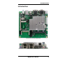
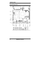
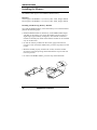
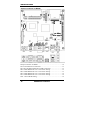
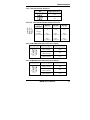
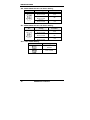
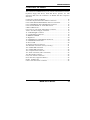
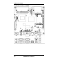
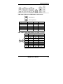
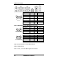
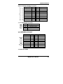
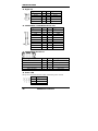
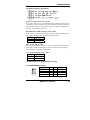
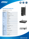
MI888 Intel® Pineview-M/ Pineview-D +ICH8M Luna-Pier / Luna-Pier Refresh Platform MiniITX Motherboard USER’S MANUAL Version 1.0 Acknowledgments AMI BIOS is a trademark of American Megatrends Inc. PS/2 is a trademark of International Business Machines Corporation. Intel and Atom are registered trademarks of Intel Corporation. Microsoft Windows is a registered trademark of Microsoft Corporation. Winbond is a registered trademark of Winbond Electronics Corporation. All other product names or trademarks are properties of their respective owners. ii MI888 User’s Manual Table of Contents Introduction .......................................................5 Checklist.............................................................................. 6 MI888 Specifications .......................................................... 7 Board Dimensions ............................................................... 8 Installations .......................................................9 Installing the Memory ....................................................... 10 Setting the Jumpers ........................................................... 11 Connectors on MI888........................................................ 15 MI888 User’s Manual iii This page is intentionally left blank. iv MI888 User’s Manual INTRODUCTION Introduction MI888 MINI ITX MOTHERBOARD MI888 EDGE CONNECTORS MI888 User’s Manual 5 INTRODUCTION Checklist Your MI888 package should include the items listed below. The MI888 Intel® Luna-Pier Mini-ITX motherboard This User’s Manual 1 CD containing chipset drivers and flash memory utility Cable kit (USB, Serial port, Serial ATA) 6 MI888 User’s Manual INTRODUCTION MI888 Specifications Form Factor CPU Type CPU Speed Green /APM BIOS Chipset Memory VGA LVDS LAN USB Serial ATA Ports Parallel IDE Audio LPC I/O Digital IO KB/Mouse Connector Expansion Slots Edge Connector On Board Header/Connecto r Watchdog Timer Power Connector Board Size MiniITX Intel® Pineview-M & Pineview-D Microprocessor (45nm Technology) Atom SC N450 1.66 GHz/ 512KB L2 cache (MI888) Atom DC D510 1.66GHz / 1MB L2 cache (MI888-D5) APM1.2 AMI BIOS, support ACPI Function Intel® Luna-Pier / Luna-Pier Refresh platform Pineview-M : 22mm x 22mm, Micro-FCBGA8 (5.5W) or Pineview-D : 22mm x 22mm, Micro-FCBGA8 ( 13W for DC) ICH8M: 31mm x 31mm, 676-pin T-PBGA (2.4W) DDR2 667MHz N450 supports SO-DIMM x 1 (w/o ECC), Max. 1GB , Single channel D510 supports SO-DIMM x 1 (w/o ECC), Max. 2GB , Single channel Intel® Integrated Graphics Controller Luna Pier supports DirectX 9 Graphic (200MHz) Luna Pier Refresh supports DirectX 9 Graphic (400MHz) OpenGL 1.4 18-bit one channels LVDS interface w/DF13 socket x1 Realtek 8111DL x 1 ICH8M built-in USB 2.0 host controller, support 8 ports ICH8M built-in SATA controller, supports 2 ports ICH8M built-in one channel Ultra DMA 33/66/100, for CF Type II (Component side) Intel ICH8M built-in audio controller w/ Realtek ALC662 Codec Supports 5.1 CH audio (Line-out, Line-in & MIC ) Winbond W83627UHG : COM1 (RS232/422/485), COM2(RS232), COM3 (RS232), COM4 (RS232), with pin-9 with power for 4 ports (500 mA for each port) Hardware monitor (2 thermal inputs, 4 voltage monitor inputs, VID0-4 & 1 x Fan Header) 4 in & 4 out Yes Mini PCI-express socket x 1 for Wireless LAN or other module PCI + PCI-Express(1x) slot x1 PS/2 KBMS connector x 1 DB15 + DB9 Stack connector x1 for VGA+COM 1 Dual DB9 Stack connector x 1 for COM2,3 RJ45 + Dual USB stack connector x1 for LAN 1 + USB 1,2 Dual USB stack connector x 1 for USB 3, 4 Audio 3-port connector x 1 (Line-out, Line-in, MIC) 2x4 pins header x 2 for 4 USB ports LVDS ( DF13 X 1 ) Mini PCI-e connector x 1 12 pins header x1 for front audio DF11-10 pins box header x 1 for COM4 CF type II connector x 1 2x5 pins header x 1 for Digital I/O Yes (256 segments, 0, 1, 2…255 sec/min) ATX (20-pins) 170mm x 170mm MI888 User’s Manual 7 INTRODUCTION Board Dimensions 8 MI888 User’s Manual INSTALLATIONS Installations This section provides information on how to use the jumpers and connectors on the MI888 in order to set up a workable system. The topics covered are: Installing the Memory ......................................................................... 10 Setting the Jumpers.............................................................................. 11 Connectors on MI888 .......................................................................... 15 MI888 User’s Manual 9 INSTALLATIONS Installing the Memory The MI888 board supports one DDR667 DDR2 memory. Remarks: N450 supports SO-DIMM x 1 (w/o ECC), Max. 1GB , Single channel D510 supports SO-DIMM x 1 (w/o ECC), Max. 2GB , Single channel Installing and Removing Memory Modules To install the DDR2 modules, locate the memory slot on the board and perform the following steps: 1. Hold the DDR2 module so that the key of the DDR2 module aligns with that on the memory slot. Insert the module into the socket at a slight angle (approximately 30 degrees). Note that the socket and module are both keyed, which means that the module can be installed only in one direction. 2. To seat the memory module into the socket, apply firm and even pressure to each end of the module until you feel it slip down into the socket. 3. With the module properly seated in the socket, rotate the module downward. Continue pressing downward until the clips at each end lock into position. 4. To remove the DDR2 module, press the clips with both hands. 10 MI888 User’s Manual INSTALLATIONS Setting the Jumpers Jumpers are used on MI888 to select various settings and features according to your needs and applications. Contact your supplier if you have doubts about the best configuration for your needs. The following lists the connectors on MI888 and their respective functions. Jumper Locations on MI888................................................................ 12 JP1: LCD Panel Power Selection ........................................................ 13 JP3, JP4, JP5: RS232/422/485 (COM1) Selection .............................. 13 JP6: COM1 RS232 RI/+5V/+12V Power Setting ............................... 13 JP8: COM4 RS232 RI/+5V/+12V Power Setting ............................... 13 JP9: COM3 RS232 RI/+5V/+12V Power Setting ............................... 14 JP7: COM4 RS232 RI/+5V/+12V Power Setting ............................... 14 JP11: Clear CMOS Setting .................................................................. 14 MI888 User’s Manual 11 INSTALLATIONS Jumper Locations on MI888 Jumper Locations on MI888 ................................................................ 12 JP1: LCD Panel Power Selection......................................................... 13 JP3, JP4, JP5: RS232/422/485 (COM1) Selection .............................. 13 JP6: COM1 RS232 RI/+5V/+12V Power Setting................................ 13 JP8: COM4 RS232 RI/+5V/+12V Power Setting................................ 13 JP9: COM3 RS232 RI/+5V/+12V Power Setting................................ 14 JP7: COM4 RS232 RI/+5V/+12V Power Setting................................ 14 JP11: Clear CMOS Setting .................................................................. 14 12 MI888 User’s Manual INSTALLATIONS JP1: LCD Panel Power Selection JP2 LCD Panel Power 3.3V 5V JP3, JP4, JP5: RS232/422/485 (COM1) Selection COM1 Function Jumper Setting (pin closed) RS-232 RS-422 RS-485 JP5: 1-2 JP5: 3-4 JP5: 5-6 JP3: 3-5 & 4-6 JP3: 1-3 & 2-4 JP3: 1-3 & 2-4 JP4: 3-5 & 4-6 JP4: 1-3 & 2-4 JP4: 1-3 & 2-4 JP6: COM1 RS232 RI/+5V/+12V Power Setting JP6 Setting Pin 1-2 Short/Closed Pin 3-4 Short/Closed Pin 5-6 Short/Closed Function +12V RI +5V JP8: COM4 RS232 RI/+5V/+12V Power Setting JP8 Setting Pin 1-2 Short/Closed Pin 3-4 Short/Closed Pin 5-6 Short/Closed MI888 User’s Manual Function +12V RI +5V 13 INSTALLATIONS JP9: COM3 RS232 RI/+5V/+12V Power Setting JP9 Setting Function Pin 1-2 Short/Closed Pin 3-4 Short/Closed Pin 5-6 Short/Closed +12V RI +5V JP7: COM4 RS232 RI/+5V/+12V Power Setting JP7 Setting Function Pin 1-2 Short/Closed Pin 3-4 Short/Closed Pin 5-6 Short/Closed +12V RI +5V JP11: Clear CMOS Setting JP11 Setting Normal Clear CMOS 14 MI888 User’s Manual INSTALLATIONS Connectors on MI888 The connectors on MI888 allows you to connect external devices such as keyboard, floppy disk drives, hard disk drives, printers, etc. The following table lists the connectors on MI888 and their respective functions. Connector Locations on MI888........................................................... 16 CN8: PS/2 Keyboard and PS/2 Mouse Connectors............................. 17 CN2: COM1 RS232/RS422/RS485 and VGA Connector................... 17 CN3: COM2/RS232 and COM3/RS232 Connector ............................ 18 CN6: 10/100/1000 RJ-45 and USB3/4 Ports...................................... 18 USB1: USB5/6 Ports ........................................................................... 18 CN7: Line-in, Line-out & Microphone Connector.............................. 18 ATX1: ATX Power Supply Connector ............................................... 19 J1: LCD Backlight Connector ............................................................. 19 J3 : LVDS(18bit) Connectors.............................................................. 19 J4: DDR2 SO-DIMM .......................................................................... 19 J5: Digital I/O ...................................................................................... 20 J6: COM2/RS232, COM3/RS232 Serial Port ..................................... 20 J7: COM4/RS232 Serial Port .............................................................. 20 J8: Power LED .................................................................................... 20 J9: System Function Connector........................................................... 21 J10: SPI Flash Connector (factory use only) ....................................... 21 J12: USB5/USB6 Connector ............................................................... 21 J13: USB7/USB8 Connector ............................................................... 22 J14: Compact Flash Connector............................................................ 22 J15: Audio Connector (DF11 Connector) ........................................... 22 J16: Mini PCIE Connector .................................................................. 22 CN4, CN5: SATA Connectors ............................................................ 22 PCI1: PCI Slot (supports 2 Master)..................................................... 22 PCIE1: PCIEX1 Slot .......................................................................... 22 FAN1: CPU Fan Power Connector ..................................................... 22 MI888 User’s Manual 15 INSTALLATIONS Connector Locations on MI888 16 MI888 User’s Manual INSTALLATIONS CN8: PS/2 Keyboard and PS/2 Mouse Connectors PS/2 Mouse PS/2 Keyboard Signal Name Keyboard data N.C. GND 5V Keyboard clock N.C. Keyboard 1 2 3 4 5 6 Mouse 1 2 3 4 5 6 Signal Name Mouse data N.C. GND 5V Mouse clock N.C. CN2: COM1 RS232/RS422/RS485 and VGA Connector Pin # Signal Name RS-232 R2-422 RS-485 [ 1 2 3 4 5 6 7 8 9 10 DCD RX TX DTR Ground DSR RTS CTS RI NC TXTX+ RX+ RXGround NC NC NC NC NC MI888 User’s Manual DATADATA+ NC NC Ground NC NC NC NC NC 17 INSTALLATIONS [[[[ VGA Signal Name Red Blue GND GND N.C. N.C. HSYNC NC Pin # 1 3 5 7 9 11 13 15 Pin # Signal Name 2 Green 4 N.C. 6 GND 8 GND 10 GND 12 N.C. 14 VSYNC CN3: COM2/RS232 and COM3/RS232 Connector Signal Name Pin # Pin # Signal Name DCD 1 6 DSR RXD 2 7 RTS TXD 3 8 CTS DTR 4 9 RI COM2/RS232 GND 5 10 Not Used [ [ COM3/RS232 Signal Name DCD RXD TXD DTR GND Pin # 1 2 3 4 5 Pin # Signal Name 6 DSR 7 RTS 8 CTS 9 RI 10 Not Used CN6: 10/100/1000 RJ-45 and USB3/4 Ports USB1: USB5/6 Ports CN7: Line-in, Line-out & Microphone Connector 18 MI888 User’s Manual INSTALLATIONS ATX1: ATX Power Supply Connector 11 1 20 10 Signal Name 3.3V -12V Ground PS-ON Ground Ground Ground -5V +5V +5V Pin # 11 12 13 14 15 16 17 18 19 20 Pin # 1 2 3 4 5 6 7 8 9 10 Signal Name 3.3V 3.3V Ground +5V Ground +5V Ground Power good 5VSB +12V J1: LCD Backlight Connector Pin # Signal Name 1 +12V 2 Backlight Enable 3 Brightness Control 4 Ground J3 : LVDS(18bit) Connectors The LVDS connectors on board Signal Name TX0Ground TX15V/3.3V NC TX2Ground TXC5V/3.3V +12V Pin # 2 4 6 8 10 12 14 16 18 20 Pin # 1 3 5 7 9 11 13 15 17 19 Signal Name TX0+ Ground TX1+ Ground NC TX2+ Ground TXC+ ENABKL +12V J4: DDR2 SO-DIMM MI888 User’s Manual 19 INSTALLATIONS J5: Digital I/O Signal Name GND OUT3 OUT2 IN3 IN2 Pin 1 3 5 7 9 Pin 2 4 6 8 10 Signal Name VCC OUT1 OUT0 IN1 IN0 J6: COM2/RS232, COM3/RS232 Serial Port Signal Name DSR RTS CTS RI NA DSR RTS CTS RI NA Pin # 2 4 6 8 10 12 14 16 18 20 Pin # 1 3 5 7 9 11 13 15 17 19 Signal Name DCD RXD TXD DTR Ground DCD RXD TXD DTR Ground Pin # 6 7 8 9 10 Signal Name DSR, Data set ready RTS, Request to send CTS, Clear to send RI, Ring indicator Not Used J7: COM4/RS232 Serial Port Signal Name DCD, Data carrier detect RXD, Receive data TXD, Transmit data DTR, Data terminal ready GND, ground Pin # 1 2 3 4 5 J8: Power LED The power LED indicates the status of the main power switch. Pin # 1 2 3 20 Signal Name Power LED No connect Ground MI888 User’s Manual INSTALLATIONS J9: System Function Connector ATX Power ON Switch: Pins 1 and 2 This 2-pin connector is an “ATX Power Supply On/Off Switch” on the system that connects to the power switch on the case. When pressed, the power switch will force the system to power on. When pressed again, it will force the system to power off. Hard Disk Drive LED Connector: Pins 3 and 4 This connector connects to the hard drive activity LED on control panel. This LED will flash when the HDD is being accessed. Pin # 4 3 Signal Name HDD Active 5V Reset Switch: Pins 5 and 6 The reset switch allows the user to reset the system without turning the main power switch off and then on again. Orientation is not required when making a connection to this header. +5V and 5VSB Signals: Pins 7 and 8 Pin # 7 8 Signal Name +5V +5VSB J10: SPI Flash Connector (factory use only) J12: USB5/USB6 Connector Signal Name Vcc DD+ Ground Pin 1 3 5 7 Pin 2 4 6 8 MI888 User’s Manual Signal Name Ground D+ DVcc 21 INSTALLATIONS J13: USB7/USB8 Connector Signal Name Vcc DD+ Ground Pin 1 3 5 7 Pin 2 4 6 8 Signal Name Ground D+ DVcc J14: Compact Flash Connector J15: Audio Connector (DF11 Connector) Signal Name Pin # Pin # LINEOUT_R 2 1 Ground 4 3 LINEIN_R 6 5 Ground 8 7 MIC-In 10 9 Ground 12 11 Signal Name LINEOUT_L JD_FRONT LINEIN_L JD_LINEIN MIC_L JD_MIC1 J16: Mini PCIE Connector CN4, CN5: SATA Connectors PCI1: PCI Slot (supports 2 Master) PCIE1: PCIEX1 Slot FAN1: CPU Fan Power Connector This is a 3-pin header for system fans. The fan must be a 12V (500mA). Pin # 1 2 3 22 Signal Name Ground +12V Rotation detection MI888 User’s Manual