1
Contents
2-33
2-34
2-35
2-36
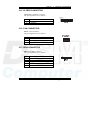
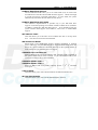
SSD Memory Mapping Selection …………………….
IRQ12 Release Selection ……………………………...
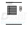
LVDS LCD Connector ………………………………..
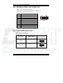
LVDS Panel Power Selection ………………………...
CHAPTER
3-1
3-2
3-3
3-4
3-5
3-6
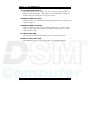
SOFTWARE UTILITIES
Introduction ...................................................................
VGA Driver Utility .......................................................
Flash BIOS Update .......................................................
LAN Driver Utility …...................................................
Sound Driver Utility …………………………………..
Watchdog Timer Configuration ....................................
CHAPTER
4-1
4-2
4-3
4-4
4-5
4-6
4-7
4-8
4-9
4-10
4-11
4-12
4-13
4-14
4-15
3
4
A
B
4-2
4-3
4-4
4-8
4-12
4-16
4-19
4-22
4-24
4-25
4-26
4-26
4-27
4-28
4-29
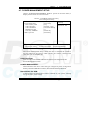
EXPANSION BUS
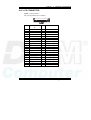
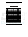
PC/104 Plus Bus Connector Pin Assignment ...........................
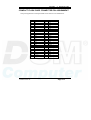
Compact Flash Card Connector Pin Assignment .....................
APPENDIX
3-2
3-2
3-3
3-5
3-7
3-8
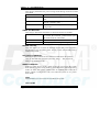
AWARD BIOS SETUP
Introduction ...................................................................
Entering Setup ...............................................................
The Standard CMOS Features ……..............................
The Advanced BIOS Features …...................................
Advanced Chipset Features ...........................................
Integrated Peripherals ……...........................................
Power Management Setup ............................................
PNP/PCI Configuration ………………………………
PC Health Status ………………………………………
Frequency/Voltage Control …………………………
Load Fail-Safe Defaults ................................................
Load Optimized Defaults ..............................................
Password Setting ...........................................................
Save & Exit Setup .........................................................
Exit Without Saving ......................................................
APPENDIX
2-23
2-23
2-24
2-24
A-2
A-3
TECHNICAL SUMMARY
Block Diagram .........................................................................
Interrupt Map ............................................................................
RTC & CMOS RAM Map .......................................................
Timer & DMA Channels Map ..................................................
I/O & Memory Map .................................................................
B-2
B-3
B-4
B-5
B-6