1
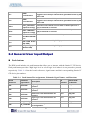
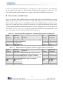
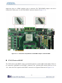
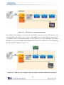
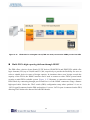
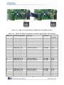
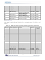
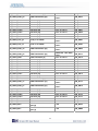
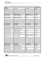
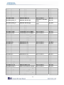
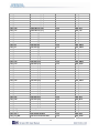
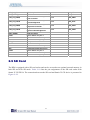
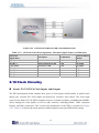
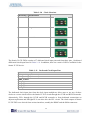
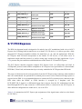
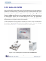
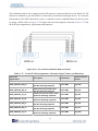
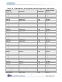
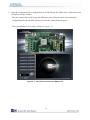
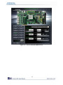
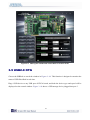
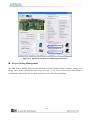
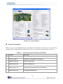
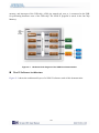
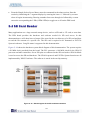
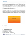
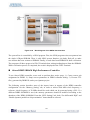
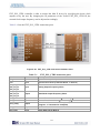
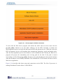
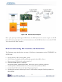
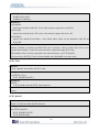
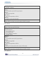
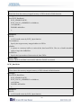
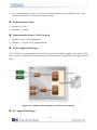
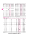
A CPU reset push-button (CPU_RESET_n) is an input to the Stratix IV GX device. It is intended to be the master reset signal for FPGA designs loaded into the Stratix IV GX device. The RE_CONFIGn push-button is used to force a reboot on the MAX II EPM2210 CPLD device. Slide Switches and DIP Switch There are also four slide switches and one 8-position DIP switch on the DE4 board to provide additional FPGA input control. Each switch is connected directly to a pin of the Stratix IV GX FPGA. When a slide switch is in the DOWN position or the UPPER position, it provides a low logic level or a high logic level to the FPGA, respectively. For 8-position DIP switch, when a switch is in the DOWN position or the UPPER position, it provides a high logic level or a low logic level to the FPGA. Table 2–5 and Table 2–6 lists the signal names and their corresponding Stratix IV GX device pin numbers for slide switches and DIP switch respectively. Table 2–5 Slide Switches Pin Assignments, Schematic Signal Names, and Functions Board Schematic Reference Signal Name SW0 SW1 SW2 SW3 SLIDE_SW0 SLIDE_SW1 SLIDE_SW2 SLIDE_SW3 Table 2–6 Description I/O Stratix IV GX Standard Pin Number High logic level when SW in the UPPER 2.5-V position 2.5-V 3.0-V 2.5-V PIN_J7 PIN_K7 PIN_AK6 PIN_L7 DIP Switch Pin Assignments, Schematic Signal Names, and Functions Board Schematic Reference Signal Name SW6 SW6 SW6 SW6 SW6 SW6 SW6 SW6 SW0 SW1 SW2 SW3 SW4 SW5 SW6 SW7 Description User-Defined DIP switch connected to FPGA device. When the switch is in the ON position, a logic 0 is selected. Similarly when the switch is in the OFF position, a logic 1 is selected. 22 I/O Stratix IV GX Standard Pin Number 3.0-V 3.0-V 3.0-V 3.0-V 3.0-V 3.0-V 3.0-V 3.0-V PIN_AB13 PIN_AB12 PIN_AB11 PIN_AB10 PIN_AB9 PIN_AC8 PIN_AH6 PIN_AG6