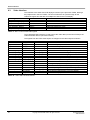
1
Application Note 227
Using the Microcontroller
Prototyping System with the
example reference design
Document number: ARM DAI0227A
Issued: August 2009
Copyright ARM Limited 2009
Application Note 227
Using the Microcontroller Prototyping System with the example reference design
Copyright © 2009 ARM Limited. All rights reserved.
Release information
The following changes have been made to this Application Note.
Change history
Date
Issue
Change
August 2009
A
First release
Version controlled by Domino.Doc DS158-GENC-009799 0.2
References
Document
Issuer
[1]
User Manual for HMALC-AS3-52
Gleichmann Industries
[2]
User Manual for Hpe-midi-V2
Gleichmann Industries
[3]
HPE_Desk-Basic Online Help
Gleichmann Industries
[4]
Altera Double Data Rate I/O Megafunctions User
Guide
Altera Corporation
[5]
The Definitive Guide to the ARM Cortex-M3
ISBN: 978-0-7506-8534-4
Elsevier (by Joseph Yiu)
[6]
PrimeCell® Synchronous Serial Port (PL022)
Technical Reference Manual
ARM Ltd.
[7]
CH7303 HDTV / DVI Transmitter (CH7303) Data
Sheet
Chrontel
[8]
ARM Dual-Timer Module (SP804) Technical
Reference Manual
ARM Ltd.
[9]
PrimeCell® Real Time Clock (PL031) Technical
Reference Manual
ARM Ltd.
[10]
ARM Watchdog Module (SP805) Technical
Reference Manual
ARM Ltd.
[11]
PrimeCell® UART (PL011) Technical Reference
Manual (Revision: r1p5)
ARM Ltd.
[12]
PrimeCell® Advanced Audio CODEC Interface
(PL041) Technical Reference Manual
ARM Ltd.
[13]
ARM PrimeCell Multimedia Card Interface
(PL181) Technical Reference Manual
ARM Ltd.
[14]
ISP1761 Hi-Speed Universal Serial Bus On-TheGo controller. Rev. 05 — 13 March 2008 Product
data sheet.
ST-NXP Wireless
ii
Copyright © 2009 ARM Limited. All rights reserved.
Application Note 227
ARM DAI0227A
Proprietary notice
ARM, ARM Powered, StrongARM, Thumb, Multi-ICE, ModelGen, PrimeCell, PrimeXsys, RealView, TrustZone, Jazelle,
ARM7TDMI, ARM9TDMI, ARMulator AMBA, and The Architecture for the Digital World are registered trademarks of ARM
Limited. Cortex, AXI, AHB, ARM7, ARM7TDMI-S, ARM7EJ-S, ARM720T, ARM740T, ARM9, ARM9TDMI, ARM920T,
ARM922T, ARM940T, ARM9E, ARM9E-S, ARM926EJ-S, ARM946E-S, ARM966E-S, ARM968E-S, ARM996HS, ARM10,
ARM1020E, ARM1022E, ARM1026EJ-S, ARM11, ARM1136J-S, ARM1136JF-S, ARM1156T2-S, ARM1156T2F-S,
ARM1176JZ-S, ARM1176JZF-S, EmbeddedICE, EmbeddedICE-RT, AMBA, ARM Development Suite, ETM, ETM7, ETM9,
ETM10, ETM10RV, ETM11, Embedded Trace Macrocell, Embedded Trace Buffer, ETB, ETB11, Embedded Trace Kit,
Integrator, JTEK, Mali, MultiTrace, MPCore, MOVE, OptimoDE, AudioDE, SecurCore, SC100, SC110, SC200, SC210, Keil,
µVision, ULINK are trademarks of ARM Limited. Java is a trademark of Sun Microsystems, Inc. XScale is a trademark of Intel
Corporation. All other brand names or product names are the property of their respective holders. “ARM” is used to represent
ARM Holdings plc (LSE: ARM and NASDAQ: ARMHY); its operating company ARM Limited; and the regional subsidiaries:
ARM, Inc.; ARM KK; ARM Korea Ltd.; ARM Taiwan Limited; ARM France SAS; ARM Consulting (Shanghai) Co. Ltd.; ARM
Belgium N.V.; AXYS Design Automation Inc.; ARM Germany GmbH; ARM Embedded Technologies Pvt. Ltd.; ARM Norway,
AS; and ARMSweden AB. Neither the whole nor any part of the information contained in, or the product described in, this
document may be adapted or reproduced in any material form except with the prior written permission of the copyright holder.
The product described in this document is subject to continuous developments and improvements. All particulars of the product
and its use contained in this document are given by ARM in good faith. All warranties implied or expressed, including but not
limited to implied warranties of satisfactory quality or fitness for purpose are excluded. This document is intended only to
provide information to the reader about the product. To the extent permitted by local laws ARM shall not be liable for any loss
or damage arising from the use of any information in this document or any error or omission in such information.
Confidentiality status
This document is Open Access. This document has no restriction on distribution.
Feedback on this Application Note
If you have any comments on this Application Note, please send email to [email protected] giving:
• the document title
•
the document number
•
the page number(s) to which your comments refer
• an explanation of your comments.
General suggestions for additions and improvements are also welcome.
ARM web address
http://www.arm.com
Application Note 227
ARM DAI0227A
Copyright © 2009 ARM Limited. All rights reserved.
iii
Table of Contents
1
INTRODUCTION .................................................................................................................. 1
1.1
Purpose of this application note .................................................................................................................. 1
1.2
Overview of the hardware platform.............................................................................................................. 1
2
HARDWARE DESCRIPTION ............................................................................................... 5
2.1
Block Diagram ................................................................................................................................................ 5
2.2
Bus Architecture of DUT FPGA .................................................................................................................... 6
2.3
Clocks and Resets ......................................................................................................................................... 7
3
PROGRAMMER’S MODEL ................................................................................................ 10
3.1
Interrupts ...................................................................................................................................................... 10
3.2
Memory map ................................................................................................................................................. 11
3.3
DUT FPGA Registers ................................................................................................................................... 11
4
FPGA DESIGN ................................................................................................................... 18
4.1
Directory structure....................................................................................................................................... 18
4.2
Re-building the DUT FPGA ......................................................................................................................... 20
4.3
Clock and reset settings ............................................................................................................................. 25
5
EXAMPLE SOFTWARE ..................................................................................................... 27
5.1
BootMonitor.................................................................................................................................................. 27
5.2
Selftest .......................................................................................................................................................... 33
6
EXTERNAL INTERFACES ................................................................................................ 37
6.1
Clocks and Resets ....................................................................................................................................... 37
6.2
Processor Interface ..................................................................................................................................... 37
6.3
Video Interface ............................................................................................................................................. 38
6.4
Human Interface ........................................................................................................................................... 39
6.5
FPGA Configuration connections .............................................................................................................. 41
6.6
SEMULATOR connections .......................................................................................................................... 41
6.7
USB Interface ............................................................................................................................................... 41
iv
Copyright © 2009 ARM Limited. All rights reserved.
Application Note 227
ARM DAI0227A
6.8
Multi-Media/SD Card Interface .................................................................................................................... 42
6.9
Audio AC97 Interface .................................................................................................................................. 43
6.10
A/D & D/A Interface ...................................................................................................................................... 43
6.11
Memory DDR Interface ................................................................................................................................ 43
6.12
Ethernet Phy Interface ................................................................................................................................. 44
6.13
CAN Interface ............................................................................................................................................... 44
6.14
Flexray Interface .......................................................................................................................................... 44
6.15
LIN Interface ................................................................................................................................................. 45
6.16
RS232 connections ...................................................................................................................................... 45
Table of Figures
Figure 1: Architecture .............................................................................................................................................. 2
Figure 2: Microcontroller Prototyping System Front Panel ................................................................................. 3
Figure 3: Microcontroller Prototyping System Rear Panel .................................................................................. 3
Figure 4: Microcontroller Prototyping System Inside ........................................................................................... 4
Figure 5: Block diagram of the ARM Microcontroller Prototyping System. ....................................................... 5
Figure 6: Bus Architecture of DUT FPGA............................................................................................................... 6
Figure 7: MPS Clock and Reset Architecture ........................................................................................................ 7
Figure 8: Hpe_desk clock factory configuration ................................................................................................... 8
Figure 9: Interrupt Allocation Table ...................................................................................................................... 10
Figure 10: DUT FPGA memory map ...................................................................................................................... 11
Figure 11: 7 Segment Display Segment Identification........................................................................................ 13
Figure 12: Timing Diagram of the I2Cbus ............................................................................................................ 14
Figure 13: Top level directory structure ............................................................................................................... 18
Figure 14: peripherals directory structure ........................................................................................................... 19
Figure 15: fpgu dut directory structure ................................................................................................................ 20
Figure 16 Top level directory structure ................................................................................................................ 27
Figure 17: BootMonitor directory structure ......................................................................................................... 33
Figure 18: Selftest directory structure ................................................................................................................. 35
Figure 19: Video DDR interface ............................................................................................................................. 39
Figure 20: HUMI logic ............................................................................................................................................. 40
Figure 21: MCI interface connections ................................................................................................................... 42
Figure 22: I2C Connections ................................................................................................................................... 43
Table of Tables
Table 1: Clock Routing ............................................................................................................................................. 9
Table 2: Reset Routing ............................................................................................................................................. 9
Table 3: dut fpga verilog files ................................................................................................................................ 20
Table 4: System Configuration .............................................................................................................................. 21
Table 5: FPGA scripts ............................................................................................................................................ 21
Table 6: Clock and Reset Destinations ............................................................................................................... 26
Table 7: Bootmonitor switch utilisation ............................................................................................................... 28
Table 8: Main Menu................................................................................................................................................. 29
Table 9: Configure Submenu ................................................................................................................................. 30
Table 10: Debug Submenu .................................................................................................................................... 31
Table 11: Flash Submenu ...................................................................................................................................... 32
Table 12: SDCard Submenu .................................................................................................................................. 32
Table 13: AACI loopback cable ............................................................................................................................. 36
Table 13: UART loopback cable ............................................................................................................................ 36
Table 15: Clocks and Resets ................................................................................................................................. 37
Table 16: Processor interface ............................................................................................................................... 37
Application Note 227
ARM DAI0227A
Copyright © 2009 ARM Limited. All rights reserved.
v
Table 17: DUT to CPU FPGA video signals .......................................................................................................... 38
Table 18: Video and LCD Connections ................................................................................................................ 38
Table 19: Human Interface .................................................................................................................................... 39
Table 20: FPGA configuration Connections ....................................................................................................... 41
Table 21: Semulator Connections ........................................................................................................................ 41
Table 22: USB Connections .................................................................................................................................. 42
Table 23: SDCard Connections ............................................................................................................................ 42
Table 24: AC97 Connections ................................................................................................................................ 43
Table 25: A/D & D/A Connections ........................................................................................................................ 43
Table 26: Memory/Childboard Connections ....................................................................................................... 44
Table 27: Ethernet Phy Connections ................................................................................................................... 44
Table 28: CAN Connections ................................................................................................................................. 44
Table 29: Flexray Connections ............................................................................................................................. 45
Table 30: LIN Connections.................................................................................................................................... 45
Table 31: RS232 Connections .............................................................................................................................. 45
vi
Copyright © 2009 ARM Limited. All rights reserved.
Application Note 227
ARM DAI0227A
Introduction
1
Introduction
The Keil Microcontroller Prototyping System (MPS) enables evaluation and
®
™
prototyping of ARM Cortex -M class processors and user defined peripherals in a single
product. The MPS is the first prototyping system incorporating a full-speed Cortex-M class
processor implemented in FPGA which can be integrated with third-party peripheral IP to
deliver a prototyping system for hardware and software application development.
The MPS enables the implementation a Cortex-M class system without needing to have
access to the processor RTL, meaning different processors can be benchmarked in order
to choose the most suitable for the intended devices price/performance. Additionally, the
MPS is delivered fully configured with the Cortex-M processor and is fully tested so that
the user does not have to test the processor implementation and can immediately begin
adding third-party IP or writing software.
1.1
Purpose of this application note
The application note explains the example DUT FPGA design, how to rebuild it and
program it into the MPS.
It will guide you through and explain the;
1. Architecture of the system
•
How the components are interconnected
•
Clock and reset structure
2. Programmers model
•
Interrupt assignment
•
Memory map
•
Peripheral register descriptions
3. FPGA design
•
structure and directory format
•
Rebuilding the FPGA image
•
Configuring Hpe®_desk and MPS
•
Programming the MPS with the new image
4. Example Software
•
BootMonitor
•
Selftest
5. Modifying the design
1.2
•
Connecting to the outside world
•
FPGA pin signal assignments
Overview of the hardware platform
The MPS was developed with two FPGAs to give the maximum flexibility for user
prototyping while maintaining IP protection of a Cortex-M class processor (to allow wide
customer accessibility without the need to license the processor). The use of the two
FPGAs allows the microcontroller, debug and memory subsystem to be implemented in
Application Note 227
ARM DAI0227A
Copyright © 2009 ARM Limited. All rights reserved.
1
Introduction
an encrypted and secure FPGA (CPU) and the user design with access to the peripheral
interfaces to be implemented in the non-encrypted FPGA (DUT).
An AHB-Lite interface from the CPU FPGA to the DUT FPGA, together with interrupts and
other sideband signals allows the DUT FPGA to interact with and be controlled by the
microcontroller as if it were a single System on Chip.
Implemented
Not Implemented
Hpe®_midiv2
Base Board
I/O
UART Switches LEDs
HMALC-AS3
Processor Board
I/O
Ethernet
I/O
Switches LEDs 7SEG
Char
LCD
Ethernet
CAN Flexray
LIN
Trace/JTAG
Trace
Debug
Interrupts
AHB Lite
CPU FPGA
DUT FPGA
Video
SMB
SMB
SSRAM
SSRAM
NOR
Video
DMB
SMB
DDR
USB
UARTS AC97 SD/MMC I2C
Video I/F
SPI
I/O
Figure 1: Architecture
The MPS has a front panel (as shown in Figure 2) fitted with;
2
•
Reset button
•
LCD character display 2 rows by 40 characters
•
4 press buttons to the DUT FPGA
•
8 LEDs from the CPU FPGA
•
8 LEDs from the DUT FPGA
•
LEDs to show if the FPGAs are over temperature
•
LEDs to show status of the power supplies
•
LEDs to show FPGAs configuration status
•
USB OTG connector for configuration/programming
Copyright © 2009 ARM Limited. All rights reserved.
Application Note 227
ARM DAI0227A
Introduction
Figure 2: Microcontroller Prototyping System Front Panel
The rear panel (as shown in Figure 3) has the following features;
•
Power connector and switch
•
USB Host and OTG ports
•
SDCard slot
•
RS232/CAN/LIN/FlexRay connections
•
10/100 Ethernet RJ45 interface
•
RGB video output port (DVI-A connector)
•
RS232 ports
•
Childboard expansion slot (red plastic plates)
•
Audio line in and line out
•
JTAG/SWD connector for ULINK-2 and other ARM debug hardware
•
External clock source (not supported at present)
•
Analogue port (not supported at present)
JTAG for
BootMonitor Console
Figure 3: Microcontroller Prototyping System Rear Panel
Application Note 227
ARM DAI0227A
Copyright © 2009 ARM Limited. All rights reserved.
3
Introduction
The inside of the MPS (as shown in Figure 3) shows the;
•
Switches, buttons and 7 segment displays
•
Location of the FPGAs (CPU and DUT)
•
IDC ribbon cables for selection of RS232/CAN/LIN/Flexray
•
Childboard connector for user expansion
•
JTAG and Trace (Mictor) connection for debug
JTAG/SWD
Trace Mictor connector
DUT User Switches
12V power to HMALC-AS3
DUT User Buttons
(Same as on front panel)
CPU User Switches[7:4]
Character LCD interface
CPU User Switches[3:0]
DUT 7 Segment display
Switch no 1, 2, 3 and 4 marked
on the package map to CPU User
Switches [0], [1], [2] and [3]
Figure 4: Microcontroller Prototyping System Inside
4
Copyright © 2009 ARM Limited. All rights reserved.
Application Note 227
ARM DAI0227A
Hardware Description
2
Hardware Description
This application note explains the example AHB (AMBA 2.0) system implemented on the
MPS. This board contains two FPGAs:
2.1
•
The CPU FPGA: An ARM Cortex-M class processor with debug and trace
support depending on the processor, two memory controllers to operate
interfaces to the noBLRAM and FLASH NOR RAM on the board, Touchscreen
2
(SPI) and Video configuration (I C) peripherals and a configuration register block.
This design is processor specific and more details can be found in the relevant
application note.
•
The DUT FPGA: Containing an example system including timers, display drivers,
an audio interface and an MCI/SD card interface.
Block Diagram
Figure 4 shows how the two FPGAs are interconnected with a 32bit AHB-Lite interface
between the CPU and the DUT FPGAs, also sideband signals and interrupts between the
FPGAs dependant on the processor implemented to enable a realistic system in the DUT
FPGA.
Implemented
Not Implemented
Hpe®_midiv2
Base Board
I/O
I/O
Switches LEDs 7SEG
UART Switches LEDs
HMALC-AS3
Processor Board
Ethernet
Char
LCD
Ethernet
I/O
CAN Flexray
LIN
Trace/JTAG
Trace
Debug
Interrupts
CPU FPGA
DUT FPGA
AHB Lite
Video
SMB
SMB
SSRAM
SSRAM
NOR
Video
DMB
SMB
DDR
USB
Video I/F
UARTS AC97 SD/MMC I2C
SPI
I/O
Figure 5: Block diagram of the ARM Microcontroller Prototyping System
Application Note 227
ARM DAI0227A
Copyright © 2009 ARM Limited. All rights reserved.
5
Hardware Description
Bus architecture
2.2
Bus Architecture of DUT FPGA
An AHB-Lite system is implemented in the DUT FPGA to give the processor access to all
the AHB peripherals within the FPGA. An AHB to APB bridge allows implementation of
APB peripherals in the system also.
0x4000_0000
0xDFFE_FFFF
0xE010_0000
0xFFFF_FFFF
AHB Interface from
CPU FPGA
External Device
CPU FPGA
DUT FPGA
I/O PADS
CPU FPGA
I/O PADS
AHB Lite Data Mux and address decode
0x4000_0000
0x5FFF_FFFF
Video config reg
0xA000_0000
0xDFFF_FFFF
0xE010_0000
0xFFFF_FFFF
Video
Controller
User Supplied
0x6000_0000
0x9FFF_FFFF
Video
Ethernet
Ethernet
Reserved
LIN
Reserved
CAN
Reserved
Flexray
SMC
DMC (DDR I/II)
User Supplied
System
I/O PADS
I/O PADS
AHB to APB
I/O PADS
DMC config reg
DDR I/II
SMC config reg
SRAM/NOR
DUT Char LCD
Character LCD
I2C (1)
I2C
PL041
AACI/AC97
PL011 (2)
UART (1)
PL011 (0)
UART (0)
PL181
0x6000_0000
0x9FFF_FFFF
Switches/LEDs config
Timer[3:2]
SP804 (0)
Timer[1:0]
SP805 (0)
External memory
SD/MMC
SP804 (1)
PL031
0xA000_0000
0xA03F_FFFF
UART (2)
PL011 (1)
DUT Config Regs
USB
RTC
WatchDog
Figure 6: Bus Architecture of DUT FPGA
6
Copyright © 2009 ARM Limited. All rights reserved.
Application Note 227
ARM DAI0227A
Hardware Description
2.3
Clocks and Resets
Figure 7 below shows the Clock factory which is a simple switch matrix to select any of
the input clock sources and route them to the output clocks for distribution to the CPU and
DUT FPGAs.
Hpe®_midiv2
Base Board
MCB0_1/33/65/66
CLK0/1/Ext/MOD
HMALC-AS3
Processor Board
CPU_PLL_R2/L2_CLKOUT0
DUT_PLL_R2_CLKOUT0
CPU_PLL_T1/B1_CLKOUT3
DUT_PLL_T1/B1_CLKOUT3
MCB0_B58/PWR_RESET#
MCB0_B60/USER_RESET#
100MHz Osc
Clock Factory
MCB0_B62/HPE_RESET#
CLK4p/13p
CLK5p/15p
CLK100M
CLK1p/10p (matched lengths)
DUT_PLL_T1/B1_CLKOUT3
MCB0_B34/B2
CLK1p = HCLK
CLK10p = 25MHz reference
CLK100M = 100MHz reference
PLL
PLL
L14_CPUCLK_Diff
L14_DUTCLK_Diff
CPU FPGA
DUT FPGA
USER_RESET#
HPE_RESET#
Figure 7: MPS Clock and Reset Architecture
The user has control of the input clocks from the DUT FPGA (e.g.
DUT_PLL_R2_CLOCKOUT0) and can use PLLs within the FPGA to set operating
frequencies and drive these signals to the clock factory. The clock factory can then route
these signals back to either or both the CPU and DUT FPGA (e.g. CLK15p) to allow
changes of clock frequency etc on FPGA clock input pins.
Application Note 227
ARM DAI0227A
Copyright © 2009 ARM Limited. All rights reserved.
7
Hardware Description
Figure 8: Hpe_desk clock factory configuration
The configuration of the clock factory is performed using Hpe_desk and is a simple button
selection matrix to define the routing of clocks. Figure 8 shows the selection of source
clock CPU_PLL_R2_CLKOUT0 (from CPU FPGA) driving the destination clock
CLKF_CLK1 back into both CPU and DUT FPGA.
CLKF_CLK100M is the default 100MHz clock source and should be used as the
reference for all PLL generated clocks.
2.3.1
Clock Routing
Name
CLK100M
CLK0
CLK1
EXT
CLK5p
CLK15p
CLK1p
CLK10p
CLK4p
CLK13p
DUT_PLL_T1_CLKOUT3
DUT_PLL_B1_CLKOUT3
DUT_PLL_R2_CLKOUT0
CPU_PLL_L2_CLKOUT0
8
Source
Osc
BB
BB
BB
CF
CF
CF
CF
CF
CF
DUT
DUT
DUT
CPU
Destination
CF,DUT,CPU
CF
CF
CF
CPU
CPU
CPU,DUT
CPU,DUT
DUT
DUT
CF,CPU,MCB0
CF,CPU,MCB0
CF
CF
Note
Buffered 100MHz clock output to DUT and CPU
Oscillator module on Baseboard
Oscillator module on Baseboard
External SMB clock input on Baseboard
Direct connection to CPU only
Direct connection to CPU only
Buffered match lengths to DUT & CPU (HCLK)
Buffered match lengths to DUT & CPU (CLK25MHz)
Direct connection to DUT only
Direct connection to DUT only
Buffered FPGA output from internal PLL
Buffered FPGA output from internal PLL
Direct FPGA output from internal PLL
Direct FPGA output from internal PLL
Copyright © 2009 ARM Limited. All rights reserved.
Application Note 227
ARM DAI0227A
Hardware Description
Name
CPU_PLL_R2_CLKOUT0
CPU_PLL_B1_CLKOUT3
CPU_PLL_T1_CLKOUT3
L14_CPUCLK_Diff
L14_DUTCLK_Diff
Source
CPU
CPU
CPU
CPU
DUT
Destination
CF
CF
CF
DUT
CPU
Note
Direct FPGA output from internal PLL
Direct FPGA output from internal PLL
Direct FPGA output from internal PLL
Direct FPGA differential output for L14 interface
Direct FPGA differential output for L14 interface
Source
BB
All
CF
Destination
CF
CF,CPU,DUT
BB, DUT
Note
O/D output from supply monitor (internal use)
Push button on Processor board O/D
Driven by USER_RESET# and PWR_RESET#
Table 1: Clock Routing
2.3.2 Reset Routing
Name
PWR_RESET#
USER_RESET#
HPE_RESET#
Table 2: Reset Routing
Notes:
BB: BaseBoard
CF: Clock Factory
CPU: CPU FPGA
DUT: DUT FPGA
OSC: Crystal Oscillator module.
The System only uses the USER_RESET# signal and this drives all internal resets
(nPOR, nHRESET etc). The design ignores PWR_RESET# and HPE_RESET#.
The CPU FPGA drives the nHRESET signal between the CPU and DUT FPGA to create
a synchronous reset (with respect to HCLK) in the DUT FPGA. The DUT FPGA uses this
to resynchronise resets to all other clock domains within the FPGA.
Application Note 227
ARM DAI0227A
Copyright © 2009 ARM Limited. All rights reserved.
9
Programmer’s Model
3
Programmer’s Model
3.1
Interrupts
The interrupt controller is integrated into the processor and resides in the CPU FPGA.
Details of the architecture for this can be found in the relevant processor Application Note
and documentation. The mapping of the example system peripherals to interrupts is
irrespective of the controller implementation and detailed here. Figure 8 describes which
interrupt is driven by each peripheral. An NMI input is available on some processors and
is also shown below.
[31]
External Device
[30]
[29]
Private Peripheral
Bus
[28]
Reserved
[27]
DUT FPGA
[26]
[25]
CPU FPGA
[24]
[23]
[22]
Reserved
[21]
[20]
[19]
Reserved
I2C ADC/DAC
[18]
Reserved
LIN
[17]
Reserved
CAN
[16]
Reserved
Flexray
[15]
Char LCD
[14]
USB
USB HC
[13]
USB
USB DC
[12]
Ethernet
[11]
PL111
CLCD combined Int
[10]
PL041
AACI/AC97
[09]
Reserved
[08]
PL011 (2)
UART (2)
[07]
PL011 (1)
UART (1)
[06]
PL011 (0)
UART (0)
[05]
PL181
Character LCD
Ethernet
MCIb
[04]
PL181
[03]
SP804 (1)
Timer[3:2]
[02]
SP804 (0)
Timer[1:0]
[01]
PL031
[00]
SP805 (0)
WatchDog
NMI
SP805 (0)
WatchDog
MCIa
RTC
Figure 9: Interrupt Allocation Table
10
Copyright © 2009 ARM Limited. All rights reserved.
Application Note 227
ARM DAI0227A
Programmer’s Model
3.2
Memory map
Figure 10 details the memory ranges available to the DUT FPGA and the assignment of
memory locations for the example system.
External Device
0xC000_0000
0x10000_0000
Private Peripheral
Bus
System
(ARMv7M)
System
Bus Bus
Reserved (ARMv6M)
DUT FPGA
0xA400_0000
0xE010_0000
0xE000_0000
≈
Processor PPB
≈
SMC Reserved
0xA3FF_0000
CPU FPGA
Ext Periph non Exec
≈
0xD000_0000
Reserved
≈
0xA400_0000
Ext Periph non Exec
0xA000_0000
0xC000_0000
SMC Peripheral 0
0xA002_0000
USB (128kB)
0xA000_0000
Ext Periph non Exec
0xB000_0000
0x5000_0000
Ext Periph non Exec
0xA000_0000
0x4FFF_0000
Video
0x4FFE_0000
Ethernet
DMC (DDRII)
Ext RAM Exec
0x9000_0000
0x4FFD_0000
LIN
0x4FFC_0000
CAN
0x4FFB_0000
Flexray
Ext RAM Exec
0x8000_0000
0x4FFA_0000
Ext RAM Exec
≈
0x7000_0000
Reserved
≈
0x4FF0_0000
Ext RAM Exec
16x 64kB AHB peripherals
0x6000_0000
0x4001_0000
0x4000_F000 ≈
Periph non Exec
0x4000_E000
0x5000_0000
0x4000_D000
Periph non Exec
0x4000_0000
16x 4kB APB peripherals
DUT Char LCD
I2C (ADCDAC)
0x4000_A000
PL041
0x4000_9000
Reserved
0x4000_5000
≈
Reserved
≈
0x4000_401C
PL011 (2)
0x4000_4018
Counter100Hz
0x4000_7000
PL011 (1)
0x4000_4014
Counter25MHz
0x4000_6000
PL011 (0)
0x4000_4010
DUT 7Seg Display
0x4000_5000
PL181
0x4000_400C
DUT LEDs
0x4000_4000
DUT Sys Regs
0x4000_4008
DUT Switches
0x4000_3000
SP804 (1)
0x4000_4004
Periph Cfg
0x4000_2000
SP804 (0)
0x4000_4000
System ID
0x4000_1000
PL031
0x4000_0000
SP805 (0)
Int ROM Exec
0x0000_0000
≈
≈
0x4000_8000
Int ROM Exec
0x1000_0000
Reserved (SMC cfg)
0x4000_B000
Int RAM A Exec
0x2000_0000
Reserved
Reserved (DMC cfg)
0x4000_C000
Int RAM B Exec
0x3000_0000
≈
Figure 10: DUT FPGA memory map
3.3
DUT FPGA Registers
3.3.1
System Registers
The DUT specific registers are mapped to a 16KB area at 0x4000_4000. The addresses
in this section are all relative to this base address.
Register
SYS_ID
SYS_PERCFG
SYS_SW
SYS_LED
SYS_7SEG
SYS_CNT25MHz
SYS_CNT100Hz
Offset
‘h0000
‘h0004
‘h0008
‘h000C
‘h0010
‘h0014
‘h0018
3.3.1.1 ID register (SYS_ID)
Name
Bits
REV
31:28
BOARD
27:16
Application Note 227
ARM DAI0227A
Access
RO
RW
RO
RW
RW
RO
RO
Reset
‘h102304xx
‘h00000000
‘h000000xx
‘h00000000
‘h00000000
‘h00000000
‘h00000000
Access Reset
RO
‘h1
RO
‘h023
Note
Board and FPGA identifier
Peripheral control signals
Indicates user switch settings
Sets LED outputs.
Sets LED outputs.
Free running counter incrementing at 25MHz
Free running counter incrementing at 100Hz
Note
Board Revision B
HBI Board number
Copyright © 2009 ARM Limited. All rights reserved.
11
Programmer’s Model
VARIANT
ARCH
BUILD
15:12
11:8
7:0
RO
RO
RO
‘h0
‘h4
‘hxx
3.3.1.2 Peripheral configuration (SYS_PERCFG)
Name
Bits
Access Reset
Reserved
31:12
USB_FORCE_SLOW 11
RW
‘b0
HUMI_MODE
10:8
RW
‘b000
USB_HC_WAKE
7
RO
‘bUSB_DC_WAKE
6
RO
‘bReserved
Reserved
Reserved
Reserved
WPROT
CARDIN
5
4
3
2
1
0
RO
RW
RW
RO
RO
RO
‘b0
‘b0
‘b0
‘b0
‘b0
‘b0
Build Variant of board
Bus Architecture (4 AHB)
FPGA build
Note
Forces the USB interface to operate slowly
Operation mode of HUMI multiplexer (see table)
Status of USB Host Controller Wake/Suspend signal
Status of USB Device Controller Wake/Suspend
signal
Status of MCI WPROT bit, 1 write protected
Status of MCI card Present, 1 card inserted
The Human Interface (HUMI) Mode bits define how the scheduler selects the different
display components on the system. This can be used for system debug.
Mode
Scheduler
LEDs
7Segment 0
7Segment 1
7Segment 2
7Segment 3
Character LCD
Reserved
Bit value
000
001
010
011
100
101
110
111
3.3.1.3 Switches (SYS_SW)
Name
Bits
Reserved
31:8
USER_BUT[3:0]
7:4
USER_SW[3:0]
3:0
3.3.1.4 LEDs (SYS_LED)
Name
Bits
Reserved
31:8
LED
7:0
Note
Round robin schedule to all HUMI devices
HUMI LEDs only output
HUMI 7Segment display 0 only output
HUMI 7Segment display 1 only output
HUMI 7Segment display 2 only output
HUMI 7Segment display 3 only output
HUMI character LCD only output
Reserved - Do Not Use
Access Reset
Note
RO
RO
Always returns value of user buttons
Always returns value of user switches
Access Reset
Note
RW
‘h00
Returns value in register. 1 is LED on 0 LED off
Reset
‘h00
‘h00
‘h00
‘h00
Note
Segments for display 3
Segments for display 2
Segments for display 1
Segments for display 0
3.3.1.5 Display output (SYS_7SEG)
Name
Bits
Access
DISP3
31:24
RW
DISP2
23:16
RW
DISP1
15:8
RW
DISP0
7:0
RW
12
‘h‘h-
Copyright © 2009 ARM Limited. All rights reserved.
Application Note 227
ARM DAI0227A
Programmer’s Model
Disp3
Disp2
Disp1
Disp0
A
A
A
A
B
F
B
F
G
G
C
E
D
P
D
D
P
D
G
C
E
B
F
G
C
E
B
F
D
C
E
D
P
D
D
P
Figure 11: 7 Segment Display Segment Identification
Name
DP
G
F
E
D
C
B
A
Bit
7
6
5
4
3
2
1
0
Note
1 is Decimal Point on, 0 is Decimal Point off.
1 is segment on, 0 is segment off.
1 is segment on, 0 is segment off.
1 is segment on, 0 is segment off.
1 is segment on, 0 is segment off.
1 is segment on, 0 is segment off.
1 is segment on, 0 is segment off.
1 is segment on, 0 is segment off.
3.3.1.6 25MHz Counter (SYS_CNT25MHz)
Name
Bits
Access Reset
Count25MHz
31:0
RO
‘h00000000
Note
Free running counter from 25MHz clock
3.3.1.7 100Hz Counter (SYS_CNT100Hz)
Name
Bits
Access Reset
Count100Hz
31:0
RO
‘h00000000
Note
Free running counter from 100Hz clock
3.3.2
2
ADC/DAC (I C)
The DS702 peripheral is used for the interface and implements a bit banging method for
2
the I C interface. The base address for this peripheral is 0x4000_B000. Refer to [2] for
further details.
Register
SB_CONTROL
SB_CONTROLS
SB_CONTROLC
Offset
‘h0000
‘h0000
‘h0004
Access
R
W
WO
Reset
‘b0‘b00
‘b00
3.3.2.1 SB Status register (SB_CONTROL)
Name
Bits
Access Reset
Reserved
31:2
SB_SDA (data wire) 1
RO
‘b0
Application Note 227
ARM DAI0227A
Note
Status Register of I/O signals
Set Output bits
Clear Output bits
Note
Level of SDA signal
Copyright © 2009 ARM Limited. All rights reserved.
13
Programmer’s Model
SB_SCL (clk wire)
0
RO
‘b0
3.3.2.2 SB Set register (SB_CONTROLS)
Name
Bits
Access Reset
Reserved
31:2
SB_nSDAOUTEN
1
W
‘b0
SB_SCLOUT
0
W
‘b0
3.3.2.3 SB Clear register (SB_CONTROLC)
Name
Bits
Access Reset
Reserved
31:2
SB_nSDAOUTEN
1
W
‘b0
SB_SCLOUT
0
W
‘b0
Level of SCL signal
Note
Sets SDA line when 1
Sets SCL line when 1
Note
Clears SDA line when 1
Clears SCL line when 1
3.3.2.4 Basic Timing
2
The basic I C (Inter-Integrated Circuit) timing diagram is shown in Figure 11.The ACK is a
returned value from the target device (responding to a data burst being received).
SDA
LSB
MSB
ACK
SCL
Stop
Start
2
Figure 12: Timing Diagram of the I Cbus
3.3.3
Character LCD
The Character display component is the DS700 and interfaces to the industry standard
Hitachi HD44780 controller. It uses 11 signals 8 data, 1 strobe (E), read/write (RnW) and
Register/data select (RS).
Note: the interface can be a 4-bit or 8-bit interface. For this application it is in 8-bit mode.
Note: When the display is used with a 4-bit interface an 8-bit value has to be written/read
as two consecutive nibbles, writing/reading bits [7:4] first into register bits [7:4], then
writing/reading bits [3:0] into register bits [7:4].
Register
CHAR_COM
Offset
‘h0000
Access Reset
RW
‘h00000000
CHAR_DAT
‘h0004
RW
‘h00000000
CHAR_RD
‘h0008
RO
‘h00000000
CHAR_RAW
‘h000C
RW
‘h00000000
CHAR_MASK
‘h0010
RW
‘h00000000
CHAR_STAT
‘h0014
RO
‘h00000000
Note
A write will write to the display controller command
register. A read will initiate a status register access
(returns value later in CHAR-RD).
A write will write to the display controller data register.
A read will initiate a data register access (returns
value later in CHAR-RD).
Contains data from last CHAR_COM or CHAR_DAT
read when CHAR_RAW[8] is set.
Reading bit 8 indicates if access is complete. Writing 0
to bit 8 clears bit.
Set bit 0 to 1 will generate interrupt when access
completes.
Returns status of Access Complete ANDed with
CHAR MASK.
3.3.3.1 Character Command Register (CHAR_COM)
14
Copyright © 2009 ARM Limited. All rights reserved.
Application Note 227
ARM DAI0227A
Programmer’s Model
Name
Reserved
COMMAND
Bits
31:8
7:0
Access Reset
RW
‘h00000000
RW
‘h00000000
Note
A write will write to the display controller command
register. A read will initiate a status register access
(returns value later in CHAR_RAW and CHAR-RD).
3.3.3.2 Character Data Register (CHAR_DAT)
Name
Reserved
DATA
Bits
31:8
7:0
Access Reset
RW
‘h00000000
RW
‘h00000000
Note
A write will write to the display controller data register.
A read will initiate a data register access (returns value
later in CHAR_RAW and CHAR-RD
3.3.3.3 Character RD Register (CHAR_RD)
Name
Reserved
READ
Bits
31:8
7:0
Access Reset
RO
‘h00000000
RO
‘h00000000
Note
Contains data from last CHAR_COM or CHAR_DAT
read when DONE is set.
3.3.3.4 Character Command Register (CHAR_RAW)
Name
Reserved
DONE
Bits
31:9
8
Access Reset
RW
‘h0000000
RW
‘b0
Reserved
7:0
RW
Note
Reading indicates if access is complete. Writing 0
clears bit.
‘h00
Note: If a transaction is attempted before DONE is asserted (CHAR_RAW register) by the
controller then it may be ignored and the command/data transfer could be lost. Once
DONE is asserted it can be cleared and a transaction started.
3.3.3.5 Character Interrupt Mask Register (CHAR_MASK)
Name
Reserved
MASKINT
Bits
31:1
0
Access Reset
RW
‘h00000000
RW
‘b0
Note
Set to 1 will generate interrupt when access completes
(CHAR_DONE set)
3.3.3.6 Character Status Register (CHAR_STAT)
Name
Reserved
STATINT
Application Note 227
ARM DAI0227A
Bits
31:1
0
Access Reset
RW
‘h00000000
RW
‘b0
Note
Returns status of CHAR_DONE ANDed with
CHAR_MASKINT.
Copyright © 2009 ARM Limited. All rights reserved.
15
Programmer’s Model
3.3.4
Video
This is a user supplied component with basic interfaces brought into the DUT FPGA to
enable implementation.
2
The DVI-I controller device (Chrontel CH7302) uses an I C serial bus for configuration
this is implemented in the CPU FPGA using the DS702.
The example clock source for the video pixel clock is derived from the PLL in the DUT
FPGA and drives a clock input of the DUT FPGA (CLK4p) via the clock factory. The clock
source is set by the Hpe_Desk application on the PC and the frequency is determined by
the PLL implemented in the DUT FPGA.
For further data on the video encoding see the Datasheet for Chrontel CH7302 [7].
3.3.5
Timer
The SP804 ADK component is used for the timers. See the TRM for details about its
functionality [8]. The Timer clock is set at 1MHz and is derived from the 100MHz clock.
The combined interrupt is used so each SP804 implementation only has 1 interrupt output
(see section 3.1).
3.3.6
RTC
The PL031 PrimeCell is used as the RTC. See the TRM for details about its functionality
[9]. The RTC clock is feed from the RTCCLK signal and is 1Hz and is derived from the
100MHz clock.
3.3.7
WatchDog
The SP805 ADK component is used for the watchdog. See the TRM for details about its
functionality [10]. The clock is set at 1Hz and is derived from the 100MHz clock.
3.3.8
Dynamic Memory Controller
This is a user supplied component with basic interfaces brought into the DUT FPGA to
enable implementation.
3.3.9
Static Memory Controller
The Static memory interface implemented in the design is specifically to allow
communication to the ISP1761 USB device [14]. It does not require any configuration and
is optimized for operation with a 50MHz AHB interface.
3.3.10 UARTs
The PL011 PrimeCell is used as the UART. See the TRM for details about its functionality
[11].
The clock is set at 25MHz and is derived from the 100MHz clock.
3.3.11 Audio (AACI/AC97)
The PL041 PrimeCell is used as the AACI. See the TRM for details about its functionality
[12]. The AACI is a modification of the PrimeCell with increased FIFO depth to help
improve transfer performance in FPGA.
The clock source is derived from the baseboard and drives a clock input of the DUT
FPGA (CLK13p). The FPGA can also drive the AC_EXT_CLK to set the clock, but this
option is not implemented in the example system.
16
Copyright © 2009 ARM Limited. All rights reserved.
Application Note 227
ARM DAI0227A
Programmer’s Model
3.3.12 MMC/SD (MMCI)
The PL181 PrimeCell is used as the MMC/SD card controller. See the TRM for details
about its functionality [13]. The MMCI uses the bits in the system registers to identify the
write protection and card inserted status (see section 3.3.1 for details).
Application Note 227
ARM DAI0227A
Copyright © 2009 ARM Limited. All rights reserved.
17
FPGA Design
4
FPGA Design
All of the RTL for this design is provided as Verilog or precompiled netlists. Example files
are provided to allow the system to be rebuilt with the Altera Quartus II tools. The readme
files provided with the application note show the version of the tools used to build the
design.
4.1
Directory structure
Figure 13: Top level directory structure
The directory structure is separated as follows:
4.1.1
•
docs:
Contains related documents including this document
•
fpga_cpu:
Contains precompiled encrypted images for the CPU FPGA in the
design which contains the processor.
•
fpga_dut:
Contains the verilog RTL files which describe the structure and
design of the example system in the DUT FPGA.
•
software:
bootmonitor and selftest example software.
•
peripherals : Contains the verilog RTL or precompiled images of the peripherals
used by the example design design In the DUT FPGA.
Peripherals
The peripherals used in the example system are stored in the peripherals directory which
contains either verilog source or netlists. These files are read by the synthesis tool at run
time and used to create a netlist for place and route. Each peripheral has its own directory
under either logical (for Verilog source) or physical (for netlists).
18
Copyright © 2009 ARM Limited. All rights reserved.
Application Note 227
ARM DAI0227A
FPGA Design
logical
ds700_charlcd
verilog
Verilog source files
ds702_i2c
verilog
Verilog source files
ds704_videogen
verilog
Verilog source files
pl011_uart
verilog
Verilog source files
pl022_ssp
verilog
Verilog source files
pl031_rtc
verilog
Verilog source files
sp804_timer
verilog
Verilog source files
sp805_watchdog
verilog
Verilog source files
physical
pl041_aaci
synplify
netlist
Netlist files
pl181_mmci
synplify
netlist
Netlist files
Figure 14: peripherals directory structure
The description of each peripheral is outside the scope of this application note. The TRM
for each peripheral can be found within each peripheral’s folder and should be referenced
for details about the operation and programmers model.
These peripheral files are supplied as an example for use in the example system.
4.1.2
DUT FPGA
The following directory structure shows the position of the files required to re-build the
DUT FPGA image for the MPS.
Application Note 227
ARM DAI0227A
Copyright © 2009 ARM Limited. All rights reserved.
19
FPGA Design
fpga_dut
logical
verilog
Verilog source files
physical
mpb_dut
altera
netlist
Build files and FPGA
image
scripts
Scripts to rebuild the
FPGA image
Figure 15: fpgu_dut directory structure
4.2
Re-building the DUT FPGA
4.2.1
Design file description
The fpga_dut directory contains the Verilog source required for the top-level of the
example system. This directory together with the peripherals directory contains all the
files required to build the example system. A description of each file is given in Table 3.
Filename
AHB2APB.v
AHBAPBSys_dut.v
AHBDecoder_dut.v
AHBDefaultSlave.v
AHBMuxS2M.v
AHBUSBController.v
APBDecoder.v
APBRegs_dut.v
clock_divider.v
dut_logic.v
fpga_dut.v
fpga_dut_defs.v
humi_mux.v
pulse_gen.v
Note
AHB to APB bridge
APB subsystem, instantiates the AHB to APB bridge, APB address decoder and
APB peripherals. This requires changes to add or remove APB peripherals
AHB address decoder. This requires changes to add or remove AHB peripherals
Creates the error response if a unmapped AHB address is accessed
AHB multiplexer to direct the correct AHB peripheral access to the processor. This
requires changes to add or remove AHB peripherals
AHB to 16bit static memory interface to access the USB controller
APB address decoder. This requires changes to add or remove APB peripherals
APB system registers used for system control. See section 3.3.1 for details
Generates peripheral clocks derived from 25MHz reference clock
AHB subsystem, instantiating the AHB peripherals and APB subsystem
Top level, instantiating the AHB subsystem, Clock and reset logic, I/O functions (tristate, I/O registers, PLL’s etc) and Human Interface multiplexer
Defines for use by the design as compilation. See section 4.2.2 for details
Human Interface multiplexer to drive 7 segment displays, LEDS and Character LCD
Pulse generator to create enable pulses for counters, deriving the pulse from the
reference clock
Table 3: dut fpga verilog files
Also within this directory is the script for building the images to download to the FPGA.
The synthesis script is in physical/MPS_dut/altera/scripts and produces a routed, placed
design in the physical/MPS_dut/altera/netlist directory. See the Hpe_desk manuals for
downloading this image to the FPGA [2].
4.2.2
Configuring the Example System
The example system has a definitions file (fpga_dut_defs.v) in the fpga_dut/logical/verilog
directory to allow the selection of section of the design to be implemented or removed. It
20
Copyright © 2009 ARM Limited. All rights reserved.
Application Note 227
ARM DAI0227A
FPGA Design
also contains defines to determine the functionality of different sections of the design. The
description of the `defines is given in Table 4: System Configuration.
Define
`define ARM_MPS_INCLUDE_CLCD
`define
`define
`define
`define
`define
`define
ARM_MPS_VGA
ARM_MPS_SVGA
ARM_MPS_XVGA
ARM_MPS_INCLUDE_AACI
ARM_MPS_INCLUDE_MCI
ARM_MPS_INCLUDE_DMC
`define ARM_MPS_DUT_SYS_ID_REG
Note
This includes the Colour LCD and Video controller block (user supplied).
Without this define, the pixel clock is not driven and the data and control
lines are tied to ‘0’, which means that the video bus will not drive any data
or clock
Implement the VGA Pattern Generator 640x480 if no CLCD present
Implement the VGA Pattern Generator 800x600 if no CLCD present
Implement the VGA Pattern Generator 1024x768 if no CLCD present
This includes the Primecell PL041 (Audio Codec interface).
This includes the Primecell PL181 (MMC/SD interface).
This includes the DDR memory interface (user supplied).
If these components are not included then the video and LCD controller
does not have any route to memory so the address out of the video and
LCD controller block is connected to the read data bus giving a static
image on any screen attached to that interface
This is the value shown in the SYS_ID register (see section 3.3.1.1for
details)
Table 4: System Configuration
By default, the audio codec and MMC/SD card interfaces are implemented and the DMC
and CLCD are not implemented. By un-commenting or commenting the `defines, the
system configuration can be altered.
4.2.3
Building the FPGA image
To rebuild the image and download to the MPS the Altera Quartus II tools (version 8.1 or
later) and the Hpe®_desk application need to be installed on the PC being used. Please
refer to the MPS QuickStart guide for details on installing these.
Once the software is installed the example system FPGA image can be rebuilt by running
a single batch script. This script invokes the Altera Quartus II tools to perform both
synthesis and place and route functions. Once this script has completed, the FPGA image
file (fpga_dut.sof) can be download to the DUT FPGA using the Hpe®_desk application.
The files in the scripts directory (fpga_dut\physical\MPS_dut\altera\scripts) perform the
functions described in Table 5: FPGA scripts;
Filename
Build.bat
fpga_dut.qpf
fpga_dut.qsf
fpga_dut.sdc
Note
Windows batch file to rebuild the FPGA image in the netlist directory
Quartus II project file. This should not be altered
Quartus II TCL script. It defines the FPGA pin assignment, instantiation of pullup or
down resistors, files to be synthesised. This will require changes when modifying the
DUT FPGA design and adding or removing peripherals
Defines the timing constraints for the design and is configured to ensure operation
with the example peripherals and processor (CPU FPGA). This will require changes
when modifying the DUT FPGA design and adding or removing peripherals
Table 5: FPGA scripts
An explanation of the files contents (in Table 5: FPGA scripts) is beyond the scope of this
application note and reference to the Altera Quartus II documentation is advised for
details on the commands and structure of the files.
To build the FPGA image perform the following tasks;
1. Run the ‘build.bat’ file from the ‘fpga_dut\physical\MPS_dut\altera\scripts’
directory.
2. Check the FPGA image has been created by looking for the file ‘fpga_dut.sof’ in
the ‘fpga_dut\physical\MPS_dut\altera\netlist’ directory.
Application Note 227
ARM DAI0227A
Copyright © 2009 ARM Limited. All rights reserved.
21
FPGA Design
4.2.4
Configuring the MPS and Hpe®_desk
Before you can download the FPGA image to the MPS, the Hpe®_desk application needs
to be installed and configured. Follow the following steps to configure;
1. Ensure the Hpe®_desk application has been installed.
2. Connect the PC via a USB cable to the USB OTG connector on the front of the
MPS.
3. Power on the MPS.
4. Start the Hpe®_desk application.
5. Configure the connection method to the MPS
Select from the drop down menus, ‘Settings -> Hpe_desk Options…’
Select the ‘Hardware Settings’ tab from the ‘options’ box and then select the
‘ALTERA_INTERFACE’ radio button. Select the ‘OK’ button to complete configuration.
6. To configure the correct FPGA module for MPS.
22
Copyright © 2009 ARM Limited. All rights reserved.
Application Note 227
ARM DAI0227A
FPGA Design
Select from the drop down menu,
‘Settings -> select FPGA module -> HMALC-AS3 -> HMALC-AS3(50)’
The Hpe®_desk application has now been configured to connect to the MPS and
downloading of FPGA images can now be done.
4.2.5
MPS FPGA image download (volatile)
Downloading directly to the FPGA is the fastest method to configure, but is a volatile
download and once the power to the MPS is removed the downloaded image is lost and
the non-volatile image is used on power up. It is recommended to try new designs using
this method before committing to a non-volatile download.
To download a volatile image to the MPS perform the following from the Hpe®_desk
application;
Select from the drop down menus, ‘ClockFactory -> Download sof file to System FPGA’
Application Note 227
ARM DAI0227A
Copyright © 2009 ARM Limited. All rights reserved.
23
FPGA Design
Navigate to and select the ‘fpga_dut.sof’ image from the netlist directory to download to
the MPS.
The Hpe®_desk application will now directly program the FPGA with the image.
The Blue LED (FPGA CONFIG D) will go out while it is being configured and turn on once
it is done and the text at the bottom of Hpe®_desk application (Log window) will inform
you that it has configured. The DUT FPGA has now been updated with the new image.
4.2.6
MPS FPGA image download (non-volatile)
Downloading to the Flash memory is a slow method, but is non-volatile and the image is
reloaded on power up. It is recommended to use this when the design is stable.
To download a non-volatile image to the MPS perform the following from the Hpe®_desk
application;
24
Copyright © 2009 ARM Limited. All rights reserved.
Application Note 227
ARM DAI0227A
FPGA Design
Select from the drop down menu ‘ClockFactory -> Download to System Flash Memory’
Navigate to and select the ‘fpga_dut.sof’ image from the netlist directory to download to
the MPS.
The Hpe®_desk application will now directly program the FPGA with the image.
The Blue LED (FPGA CONFIG D) will go out while it is being configured and turn on once
it is done and the text at the bottom of Hpe®_desk application (Log window) will inform
you that it has configured. The DUT FPGA has now been updated with the new image.
4.3
Clock and reset settings
Please use the online help of the Hpe®_desk software for details on programming the
clocks [2]. Section 2.3.1 gives a basic overview of the clock factory settings.
Application Note 227
ARM DAI0227A
Copyright © 2009 ARM Limited. All rights reserved.
25
FPGA Design
4.3.1
Clock and Reset Destinations
The following table gives the default clock frequency settings used by the example
system and which clock inputs of the DUT FPGA are used.
Device
AHB/APB infrastructure
UART
SPI
2
IC
VIDEO
AC97
SD/MMC
Character LCD
HUMI
Timer
Real Time Clock
Watch Dog
USB
Static Memory
Clock Freq
HCLK
25MHz
25MHz
HCLK
25MHz
24.576MHz
25MHz
HCLK
500Hz
1MHz
1Hz
1Hz
HCLK
HCLK
Clock ref
CLK1p
CLK10p
CLK10p
CLK1p
CLK4p
CLK13p
CLK10p
CLK1p
CLK1p
CLK10p
CLK10p
CLK10p
CLK1p
CLK1p
Reset ref
HRESETn
HRESETn
HRESETn
HRESETn
HRESETn
HRESETn
HRESETn
HRESETn
HRESETn
HRESETn
HRESETn
HRESETn
HRESETn
HRESETn
Note
Runs at CPU frequency
PL011
PL022
DS702
Video/LCD controller pixel clock
PL041
PL181
DS700
Multiplexer frequency
SP804
PL031
SP805
External IC ISP1761
Memory controller on DUT FPGA
Table 6: Clock and Reset Destinations
All the peripherals that have an AHB or APB interface have that interface running at
CLK1p.
CLK100M is used to derive all peripheral clocks where appropriate since this is a non
variable clock and ideal for timers, watchdogs etc.
The Reset column refers to the reset signal that is re-synchronised to the respective clock
domain.
26
Copyright © 2009 ARM Limited. All rights reserved.
Application Note 227
ARM DAI0227A
Example Software
5
Example Software
Under the MPS root directory you can find the software directory which contains the files
required to rebuild the BootMonitor and Selftest software. It also contains the images for
downloading to the MPS.
MPS
Mx
docs
fpga_cpu
fpga_dut
peripherals
software
Figure 16 Top level directory structure
The directory structure is separated as follows:
5.1
•
docs:
Contains related documents including this document
•
fpga_cpu:
Contains precompiled encrypted images for the CPU FPGA in the
design which contains the processor.
•
fpga_dut:
Contains the verilog RTL files which describe the structure and
design of the example system in the DUT FPGA.
•
software:
BootMonitor and selftest example software.
•
peripherals: Contains the verilog RTL or precompiled images of the peripherals
used by the example design in the DUT FPGA.
BootMonitor
This is the application that runs when the system is booted, it handles the system
initialization and has a command interpreter which accepts user input from the console to
perform the following functions.
•
Board configuration.
•
General file operations using MM/SDCards configured as FAT16 8.3 filenames.
•
Programming images into flash.
•
Loading and running another application.
•
Console supports semihosting via the debugger (not supported in MDK) or serial
port.
It supports a single processor environment in little endian mode.
The BootMonitor reads the CPU User switches 0-2 (shown in 4) on power up and uses
these to select the boot option. On delivery all the switches are set to ON and defaults to
no boot script with auto detection of console interface, either semihosting (not supported
on MDK) or UART port3 (shown in Figure 4).
SW1
ON
SW2
X
Application Note 227
ARM DAI0227A
SW3
X
Function
Normal boot
Note
Use this as default
Copyright © 2009 ARM Limited. All rights reserved.
27
Example Software
OFF
X
X
Run boot Script
X
ON
ON
X
ON
OFF
X
X
OFF
OFF
ON
OFF
This needs to be pre configured from the boot
monitor command line
Auto Select between UART port3 Detects semihosting supported debugger
and Semihosting for Console
Force UART port3 for Console
Always use UART port3 regardless of
semihosting support
Reserved
Do not use, undefined behaviour
Reserved
Do not use, undefined behaviour
Table 7: Bootmonitor switch utilisation
Note: no other switches are used by BootMonitor and are free for user use at power-up or
reset.
When the MPS is turned on, Boot Monitor will start. The character display will show the
Firmware (F/W) and Hardware (H/W) versions of the system. This is also output to the
serial port for display on the terminal, if the switches are set correctly you will now enter
the Boot Monitor command prompt on the terminal (SW[3:1] ON). The CPU LEDs (0 to 7)
will cycle a lighted bit to show the Boot Monitor is running.
Pressing the reset button on the front panel will perform a hardware reset and the system
will restart as if it had been power cycled.
5.1.1
Console via serial port
To use the serial port for the console interface to BootMonitor you will need to connect a
serial null modem cable to RS232-4 (UART port3 above the power connector) and use a
terminal emulation program (e.g. HyperTerminal) configured as 38,400 baud, 8bit data,
no parity, 1 stop bit and no flow control to talk to the MPS.
5.1.2
Commands
5.1.2.1 Main Menu
Command Format
ALIAS <alias> <command string>
Note
Create an alias command <alias> for the string of commands
in <command string>.
CD <directory path>
Change directory to the one specified in <directory path>.
CLEAR BOOTSCRIPT
Clear the current boot script. If no boot script is set then the
boot monitor will always prompt for input no matter what the
state of the 'run boot script' switch.
CONFIGURE
Enter Configure Submenu
CONVERT BINARY <binary-file>
LOAD_ADDRESS <address>
[ENTRY_POINT <address>]
Adds information required by the RUN command to execute
a binary file. The command will produce a file with the same
name as the specified binary file but with the '.exe' file
extension.
COPY <file1> <file2>
Copies file <file1> to <file2>.
CREATE <file>
Create a file <file>.
DEBUG
Enter Debug Submenu
DELETE <file>
Delete a file <file>.
28
Copyright © 2009 ARM Limited. All rights reserved.
Application Note 227
ARM DAI0227A
Example Software
DIRECTORY [<directory>]
List files in <directory>.
DISPLAY BOOTSCRIPT
Display the current boot script
ECHO <text>
Prints string <text>.
EXIT
Exits the application or submenu.
FLASH
Enter Flash Submenu
HELP [<command>]
Provides help information on <command>. If <command> is
not specified then all available commands are listed.
LOAD <image>
Loads image <image> into memory.
MKDIR <directory path>
Creates a new directory at the end of the given path
QUIT
Alias for ‘EXIT’
RMDIR <directory path>
Removes a directory at the end of the given path
RENAME <file1> <file2>
Renames file <file1> to <file2>
RUN <image>
Load image <image> into memory and run it.
SDCARD
Enter SDCard Submenu
SET BOOTSCRIPT <script>
Set the current boot script. This script will be run at system
reset if the run boot script switch is set.
TYPE <file>
Displays file <file>.
Table 8: Main Menu
Application Note 227
ARM DAI0227A
Copyright © 2009 ARM Limited. All rights reserved.
29
Example Software
5.1.2.2 Configure Submenu
Command Format
DISPLAY DATE
Note
Displays the current system date.
DISPLAY HARDWARE
Display hardware information
DISPLAY TIME
Displays the current system time.
EXIT
Exits the application or submenu.
HELP [<command>]
List commands
QUIT
Alias for ‘EXIT’
RESET [IF_REQUIRED]
Resets this system. If the optional IF_REQUIRED qualifier is
specified the system will only be reset if there has been a
configuration change made that requires a reset.
SET BAUD <port #> <rate>
Sets UART <port #> to the specified <rate>.
e.g. SET BAUD 0 9600
available ports 0-4
SET DATE <dd/mm/yy>
Sets system date in the form dd/mm/yy.
SET TIME <hh:mm:ss>
Sets system time in the form hh:mm:ss
Table 9: Configure Submenu
5.1.2.3 Debug Submenu
Command Format
DEPOSIT <address> <value>
[size]
Note
Deposit value <value> to memory at <address>, optionally
specifying the [size], it can be BYTE, HALFWORD or WORD
(defaults to WORD).
DISABLE MESSAGES
Disables debug messages
ENABLE MESSAGES
Enables debug messages
EXAMINE <address> [<size>]
Examine memory at <address> for <size> number of bytes.
EXIT
Exit
GO <address>
Run code at <address>.
HELP [<command>]
List commands
MODIFY <address> <value>
<mask> [size]
Performs a read/modify/write of memory at <address>,
combining in with <value> which will be masked with
<mask>.
The size of the transfer can be optionally specified it can be
BYTE, HALFWORD or WORD (defaults to WORD).
QUIT
Alias for 'EXIT'
30
Copyright © 2009 ARM Limited. All rights reserved.
Application Note 227
ARM DAI0227A
Example Software
START TIMER
Starts a timer which is stopped with the STOP TIMER
command.
STOP TIMER
Stop a timer pervious started with the START TIMER
command and displays elapsed time.
Table 10: Debug Submenu
5.1.2.4 Flash Submenu
Command Format
DISPLAY IMAGE <name>
Note
Display details of image <name>
ERASE IMAGE <name>
Erases image (or binary file) from flash.
ERASE RANGE <start_address>
[<end_address>]
It is only possible to erase entire blocks of flash. Therefore
the entire block of flash that contains <start_address>, the
block that contains <end_address> and all intervening blocks
will be erased.
This may mean that data before <start_address> or after
<end_address> will be erased if they are not on block
boundaries.
If the optional <end_address> parameter is not specified then
only the single block of flash that contains <start_address>
will be erased.
EXIT
Exit
HELP
List commands
LIST AREAS
List areas of flash, where an area is one or more contiguous
blocks that are of the same size and use the same
programming algorithms.
LIST IMAGES
List images in flash
LOAD <name>
Load image <name> from flash.
QUIT
Alias for 'EXIT'
RESERVE SPACE <address>
<size>
Reserves space in flash for user applications that the boot
monitor will not use.
RUN <name>
Load image <name> from flash and run it.
UNRESERVE SPACE <address>
Unreserves pervious reserved space in flash.
Application Note 227
ARM DAI0227A
Copyright © 2009 ARM Limited. All rights reserved.
31
Example Software
WRITE BINARY <file>
[NAME <name>]
[FLASH_ADDRESS <address>]
[LOAD_ADDRESS <address>]
[ENTRY_POINT <address>]
Writes a binary file to flash.
The image will be identified in flash by a name derived from
the filename, for example t:/images/boot_monitor.bin will be
called boot_monitor, and this can be overridden by using the
option NAME argument.
You can specify where in flash the image is written by using
the optional FLASH_ADDRESS argument (Note: if both
FLASH_ADDRESS and LOAD_ADDRESS are specified and
LOAD_ADDRESS is located in flash then LOAD_ADDRESS
will be used and the FLASH_ADDRESS argument will be
ignored).
The optional LOAD_ADDRESS and ENTRY_POINT
arguments allow you to specify these parameters, if
ENTRY_POINT is not specified then to defaults to the load
address.
WRITE IMAGE <file>
[NAME <name>]
[FLASH_ADDRESS <address>]
Writes an ELF image file to flash.
The image will be identified in flash by a name derived from
the file name, for example t:/images/boot_monitor.axf will be
called boot_monitor, and this can be overridden by using the
option NAME argument.
You can specify where in flash the image is written by using
the optional FLASH_ADDRESS argument (Note: if the image
is linked to run from flash then this address will be used and
the FLASH_ADDRESS argument will be ignored).
Table 11: Flash Submenu
5.1.2.5 SDCard Submenu
Command Format
FORMAT [QUICK]
[VOLUME <label>]
Note
Formats the SDCard/MMC as FAT16 with 8.3 filenames
QUICK: performs a quick format with only the FAT and
bootsector updated.
VOLUME <label> will add a Volume label to the disk as
specified in the field <label>.
INFORM
Display details SD/MMC Card
INITIALISE
If the card has been changed use this command to re
initialise it to determine it’s features before using any other
commands.
EXIT
Exit
HELP
List commands
Table 12: SDCard Submenu
5.1.3
Re-building the software
Currently, only a Windows development environment is supported. The firmware can be
built using MDK and RVCT. Figure 16 bootmonitor directory structure shows the
position of the executable files and scripts for rebuilding under both RVDS and MDK.
32
Copyright © 2009 ARM Limited. All rights reserved.
Application Note 227
ARM DAI0227A
Example Software
software
projects
bootmonitor
Firmware
Boot_Monitor
Build_keil
Executable image and
scripts to rebuild with
MDK
Build_RVDS
Scripts to rebuild with
RVDS
Debug
Executable image with
debug support
Release
Executable image
Source
Examples
Libraries required to
rebuild bootmonitor
Libraries
Platform
Build_keil
Executable image and
scripts to rebuild with
MDK
Build_RVDS
Scripts to rebuild with
RVDS
Debug
Executable image with
debug support
Release
Executable image
Source
Utility_Code
cli
elf
flash
Figure 17: BootMonitor directory structure
5.2
Selftest
The selftest code allows the user to confirm the functionality of their MPS, and provides
reference code for the example peripherals. The code tests the following peripherals:
AACI, MMCI, USB, UARTs, character LCD, LEDs, switches, SRAM memory, RTC and
system clocks/interrupts.
Selftest is designed to run on the MPS using MDK and RVDS. The user can interact with
the software operation via the Serial Console for MDK or additionally the semihosting
console window under RVDS.
The user interface displays a menu and prompts the user on how to operate each test.
For more information on exactly how each test is working, refer to the provided source
code, and readme files.
Application Note 227
ARM DAI0227A
Copyright © 2009 ARM Limited. All rights reserved.
33
Example Software
5.2.1
Re-building the software
Currently, only a Windows development environment is supported. Selftest can be built
using MDK and RVCT. Figure 17 selftest directory structure shows the location of the
executable files and scripts for rebuilding under both RVDS and MDK.
The project and executable files for selftest can be found under the
\selftest\build\Build_Keil directory. To run all the tests it is necessary to connect a number
of loopback cables to the board (for audio and UARTs).
After connecting the test harness and loading the program image into the debugger
(selftest_MPS.axf) each of the MPS peripherals may be tested individually, or altogether
using ‘Run all tests’. The tests perform register level and basic functional tests on the
MPS hardware reporting any errors found.
The source code for the tests are brought together in a single project file
\build\Build_Keil\selftest_MPS.Uv2.
The source code for each peripheral test is split into separate directories for example
\apaaci\ contains apaaci.c and apaaci.h for testing the AACI peripheral. The \main\ folder
contains main.c and common.c which provide the user menu and functions that are
common to all peripheral tests.
Note: If the default install directory is not used, then the project will have to be rebuilt in
order for the debugger to display the source code automatically.
34
Copyright © 2009 ARM Limited. All rights reserved.
Application Note 227
ARM DAI0227A
Example Software
software
projects
selftest
apaaci
apcharlcd
apclcd
apdma
apgpio
apic
apkybd
apleds
apmem
apmmci
apmouse
aprtc
apsbi
apssp
apswitch
aptimer
aptsci
apuart
apusb
build
Build_keil
Build_RVDS
Executable image and
scripts to rebuild with
MDK
Executable image and
scripts to rebuild with
RVDS
main
Figure 18: Selftest directory structure
5.2.2
Selftest test hardware
The MPS test code requires three separate cable assemblies to be connected to the
board for complete testing. Note these cables are not supplied with the MPS but details of
their connections are given here.
Application Note 227
ARM DAI0227A
Copyright © 2009 ARM Limited. All rights reserved.
35
Example Software
5.2.2.1 AACI loopback cable
The AACI test performs a loopback test from Line Level Out to Line Level In. This
requires two 3.5mm stereo jack plugs which must all be wired as follows:
Connector A
Connector B
Tip
Tip
Ring
Ring
Screen
Screen
Table 13: AACI loopback cable
Connect the cable between the line in and line out sockets on the MPS (back panel).
5.2.2.2 UART loopback cable
The two UART cables have female 9-pin D-sub connectors on either end with
connections as follows:
Connector A
Pin
Connector A Name
Connector B
Pin
Connector B name
1
N/C
1
N/C
2
RX
3
TX
3
TX
2
RX
4
DTR
6
DSR
5
GND
5
GND
6
DSR
4
DTR
7
RTS
8
CTS
8
CTS
7
RTS
9
N/C
9
N/C
Table 14: UART loopback cable
Connect one cable between the top two UART connectors and the other between the
bottom two UART connectors one the MPS rear panel.
36
Copyright © 2009 ARM Limited. All rights reserved.
Application Note 227
ARM DAI0227A
External Interfaces
6
External Interfaces
This section shows the interfaces available on the Customer DUT FPGA.
The direction of the signals is shown from the point of view of the DUT FPGA, so an O
signal goes from the DUT FPGA to the CPU FPGA (for example).
6.1
Clocks and Resets
Signal
USER_RESETn
HPE_RESETn
DUT_CLK1
DUT_CLK4
DUT_CLK10
DUT_CLK13
DUT_CLK100M
DUT_PLL_B1_CLKOUT3
DUT_PLL_R2_CLKOUT0
DUT_PLL_T1_CLKOUT3
Direction [Width]
input
input
input
input
input
input
input
output
output
output
Note
AHB system clock input
Video Pixel Clock input
Peripheral reference clock input
AACI bit clock input (x2)
Reference 100MHz input
25MHz reference clock from FPGA PLL
AACI 24.576MHz bit clock x2 from FPGA PLL
Video Pixel Clock from FPGA PLL
Table 15: Clocks and Resets
6.2
Processor Interface
This interface contains the 32bit AHB-Lite bus from the processor to the peripherals
together with interrupts to the processor and sideband signals between the processor and
peripherals.
FPGA Signal
FPGA_IC[31:0]
FPGA_IC[32]
FPGA_IC[35:33]
FPGA_IC[36]
FPGA_IC[40:37]
FPGA_IC[43:41]
FPGA_IC[45:44]
FPGA_IC[46]
FPGA_IC[78:47]
FPGA_IC[110:79]
FPGA_IC[111]
FPGA_IC[112]
FPGA_IC[113]
FPGA_IC[125:114]
L14_DUTOUT_DN[11:0]
L14_DUTOUT_DN[12]
L14_CPUOUT_DN[0]
L14_CPUOUT_DN[1]
L14_CPUOUT_DN[2]
L14_CPUOUT_DN[3]
L14_CPUOUT_DN[4]
L14_CPUOUT_DN[5]
L14_CPUOUT_DN[6]
L14_CPUOUT_DN[12:7]
L14_CPUOUT_DP[9:0]
L14_CPUOUT_CLK
Function
HWDATA[31:0]
HWRITE
HBURST[2:0]
HMASTLOCK
HPROT[3:0]
HSIZE[2:0]
HTRANS[1:0]
HSEL
HADDR[31:0]
HRDATA[31:0]
HRESP
HREADY
HRESETn
INT[11:0]
INT[23:12]
NMI
SLEEPING
SLEEPDEEP
HALTED
LOCKUP
TXEV
RXEV
WDOGRES
N/C
N/C
N/C
Note
Not used, driven high by the CPU FPGA
Interrupt signals to processor
Interrupt signals to processor
Non maskable interrupt to processor
Table 16: Processor interface
Application Note 227
ARM DAI0227A
Copyright © 2009 ARM Limited. All rights reserved.
37
External Interfaces
6.3
Video Interface
The interface to the Video and LCD displays is driven by the processor FPGA, although
the peripheral is in the DUT FPGA. The CPU FPGA acts as a pass through for the
video/LCD signals and will also de-multiplex the data for the LCD display.
FPGA Signal
L14_DUTOUT_DP[11:0]
L14_DUTOUT_DP[12]
L14_DUTOUT_CLK
L14_CPUOUT_DP[10]
L14_CPUOUT_DP[11]
L14_CPUOUT_DP[12]
Function
Video RGB[11:0]
Video Resetn
PCLK
VSync
HSync
DE
Note
DDR 24bit RGB video signals clocked by VIDEOCLK
Video Reset active low
Video Pixel clock
Video vertical sync pulse
Video horizontal sync pulse
Video data enable strobe
Table 17: DUT to CPU FPGA video signals
The multiplexed DDR interface is used to drive the video data (via the CPU FPGA) to the
video transmitter device (Chrontel CH7302).
The signals from the FPGA video inputs are mapped to the video outputs as follows.
Function
PCLK
HSync
VSync
DE
Video RGB[7:0]
Video RGB[11:8]
Video RGB[7:0]
Video RGB[7:2]
Video RGB[11:8]
Video RGB[7:0]
Video Resetn
-
LCD name
LCD_R_SHFCLK
LCD_R_HSYNC
LCD_R_VSYNC
LCD_R_M_DE
LCD_TTL_R[5:0]
LCD_TTL_G[5:0]
LCD_TTL_B[5:0]
LCD_BLON
LCD_VDON
Video Name
VIDEOCLK
VIDEOHSYNC
VIDEOVSYNC
VIDEODE
VIDEO[7:0]
VIDEO[11:8]
VIDEO[7:0]
VIDEORESETn
VIDEOHPINT
VIDEOMODE
VIDEO_I2C_SCL
VIDEO_I2C_SDA
-
Note
Video Pixel clock
Video vertical sync pulse
Video horizontal sync pulse
Video data enable strobe
Red Data DDR encoded falling edge
Green Data DDR encoded rising and falling edge
Blue Data DDR encoded rising edge
Red Data MSB’s (demux’ed by CPU FPGA)
Green Data MSB’s (demux’ed by CPU FPGA)
Blue Data MSB’s (demux’ed by CPU FPGA)
Video Reset active low
Hot Plug interrupt (Not Used)
Video Mode GPIO pin of video chip (Not Used)
Video Chip configuration bus (controlled by CPU FPGA)
Video Chip configuration bus (controlled by CPU FPGA)
Back Light On (output tied to 1 on CPU FPGA)
LCD Power On (output tied to 1 on CPU FPGA)
Table 18: Video and LCD Connections
38
Copyright © 2009 ARM Limited. All rights reserved.
Application Note 227
ARM DAI0227A
External Interfaces
L14_DUT_OUT_DP[12:0]
L14_CPU_OUT_DP[12:10]
D
QR
R QF
F
VIDEO CLOCK IN
1`b1
1'b0
Clock Buffer
DR Q
DF
R
F
VIDEO
DR Q
DF
R
F
VIDEOCLK
D
LCD_R_
Q
Q
D
Q
LCD_TTL_
Q
Figure 19: Video DDR interface
6.4
Human Interface
The Human Interface (HUMI) multiplexes the LED’s, 7 Segment displays and character
LCD together and drives them over the interface to the relevant devices.
Signal
BUTTON
DUT_DSW
DUT_HUMI_An
DUT_HUMI_Bn
DUT_HUMI_Cn
DUT_HUMI_Dn
DUT_HUMI_En
DUT_HUMI_Fn
DUT_HUMI_Gn
DUT_HUMI_DPn
DUT_HUMI_SEGn
DUT_HUMI_LEDn
DUT_LCD_REGSEL
DUT_LCD_RW
DUT_LCD_ENABLE
Direction [Width]
input[4]
input[4]
bi-dir
bi-dir
bi-dir
bi-dir
bi-dir
bi-dir
bi-dir
bi-dir
output[4]
output
output
output
output
Note
Table 19: Human Interface
Please refer to section 3.3 for details on the registers used for driving this interface. The
buttons and switches can be read via the register SYS_SW (see section 3.3.1.3).
The values held in the SYS_LED and SYS_7SEG registers (see sections 3.3.1.4 and
3.3.1.5) are driven onto this interface based upon the value held in the HUMI_MODE field
in the SYS_PERCFG register (see section 3.3.1.2).
Application Note 227
ARM DAI0227A
Copyright © 2009 ARM Limited. All rights reserved.
39
External Interfaces
Figure 20: HUMI logic
The scheduler runs at a preset rate of 500Hz and selects a new driver for the data lines
(DUT_HUMI_{A-G,DP}n) every 2 ms if the HUMI_MODE field is set to Scheduler
(3’b000). The order of the cycle is:
40
- LEDs selected
the scheduler drives DUT_HUMI_LEDn low.
- Segment 0
the scheduler drives DUT_HUMI_SEGn to 4’b1110.
- Segment 1
the scheduler drives DUT_HUMI_SEGn to 4’b1101.
- Segment 2
the scheduler drives DUT_HUMI_SEGn to 4’b1011.
- Segment 3
the scheduler drives DUT_HUMI_SEGn to 4’b0111.
Copyright © 2009 ARM Limited. All rights reserved.
Application Note 227
ARM DAI0227A
External Interfaces
- Character LCD
the scheduler drives DUT_HUMI_SEGn to 4’b1110 and
DUT_HUMI_LEDn high and enables the DUT_LCD_* interface
control lines.
Should any operation be in progress when the scheduler wishes
to switch back to the LED, then change is halted whilst the
operation completes and any new operation is prevented from
starting (the CharLCD driver appears busy to the processor).
6.5
FPGA Configuration connections
These connections are not used by the design and are for FPGA configuration only.
Signal
DUTFCP_CLK
DUTFCP_DATA
DUTFCP_PLTXT_RDY
DUT_PORSEL
Direction [Width]
input
input
input
input
Note
Table 20: FPGA configuration Connections
6.6
SEMULATOR connections
The SEmulator connector is for use by the Gleichmann SEmulator product only. The
signal assignments are shown for completeness only.
Signal
SEDUT_L4_RXN
SEDUT_L4_RXP
SEDUT_L4_RXCLKN
SEDUT_L4_RXCLKP
SEDUT_L4_TXN
SEDUT_L4_TXP
SEDUT_L4_TXCLKN
SEDUT_L4_TXCLKP
SEDUT_RESETn
Direction [Width]
input[4]
input[4]
input
input
input[4]
input[4]
input
input
input
Note
Table 21: Semulator Connections
6.7
USB Interface
This interface is driven by a dedicated interface driver (16bit Static memory interface)
which is designed to drive the NXP ISP1761 USB controller [14]. The interface driver is
not configurable and is transparent to the rest of the system. All accesses to the USB
device must be halfword accesses only.
Signal
USB_A
USB_CSn
USB_RDn
USB_WRn
USB_D
USB_DC_DACK
Application Note 227
ARM DAI0227A
Direction [Width]
output[17]
output
output
output
bi-dir[16]
bi-dir
Note
Not connected in this design.
Copyright © 2009 ARM Limited. All rights reserved.
41
External Interfaces
USB_DC_DREQ
USB_DC_IRQ
USB_DC_WAKEUPn
USB_HC_DACK
USB_HC_DREQ
USB_HC_IRQ
USB_HC_WAKEUPn
bi-dir
bi-dir
bi-dir
bi-dir
bi-dir
bi-dir
bi-dir
Not connected in this design.
Used as input only. See interrupt table.
Not connected in this design.
Not connected in this design.
Not connected in this design.
Used as input only. See interrupt table.
Not connected in this design.
Table 22: USB Connections
6.8
Multi-Media/SD Card Interface
This interface is driven by the Primecell PL181 (see section 3.3.12) and is connected to
the MM/SDCard connector on the rear panel.
Signal
SD_SCLK
SD_CD
SD_WRP
SD_IRQ
SD_CSn
SD_DAT
SD_DI
SD_DO
Direction [Width]
output
input
input
bi-dir
bi-dir
bi-dir
bi-dir
bi-dir
Note
Driven by MCICLKOUT.
See Figure 18
See Figure 18
See Figure 18
See Figure 18
See Figure 18
See Figure 18
See Figure 18
Table 23: SDCard Connections
Tri-stated driver
nMCIDATEN
{SD_CSn, SD_DAT, SD_IRQ, SD_DO}
MCIDATOUT[3:0]
MCIDATIN[3:0]
Tri-stated driver
nMCICMDEN
MCICMDOUT
SD_DI
MCICMDIN
MCICLKOUT
SD_CLK
MCIFBCLK
MCICARDIN
SD_CD
PullUp, Pulled down when card
present
MCIWPROT
SD_WRP
PullUp, Pulled down when Write
protected
Figure 21: MCI interface connections
42
Copyright © 2009 ARM Limited. All rights reserved.
Application Note 227
ARM DAI0227A
External Interfaces
The nCARDIN and WPROT signals are feed to the peripheral system registers for use as
setting interrupts and detecting the status of the signals.
6.9
Audio AC97 Interface
This interface is driven by the Primecell PL041 (see section 3.3.11) and connects to the
AC97 Codec (National Semiconductor LM4549B) which has implemented the Line-in,
line-out on the rear panel and the internal speaker.
Signal
AC_BITCLK
AC_EAPD
AC_EXT_CLK
AC_SDATAIN
AC_SDATAOUT
AC_RESETn
AC_SYNC
Direction [Width]
input
input
output
input
output
output
output
Note
12.288MHz clock from Codec
Not used
24.576MHz reference clock to Codec
Drives AACISDATAIN.
Driven by AACISDATAOUT.
Driven by AACIRESET.
Driven by AACISYNC – used as an output.
Table 24: AC97 Connections
6.10
A/D & D/A Interface
This interface is driven by the serial interface block DS702 (see section 3.3.2) and
connects to the A/D and D/A converters (Cypress CY8C27543) on the rear panel.
Signal
ADDA_CLK
ADDA_DATA
Direction [Width]
OD
bi-dir
Note
Driven by SCL.
Drives SDAin and is driven to ‘0’ by nSDAOUTEN going
to ‘0’
Table 25: A/D & D/A Connections
nSDAOUTEN
1'b0
ADDA_DATA
Tri-stated driver
SDAin
SCL
ADDA_CLK
Driver
2
Figure 22: I C Connections
6.11
Memory DDR Interface
The signals are connected to the Childboard connector. They reference standard DDR2
signals, but can be driven with different signals depending on the Childboard connected.
This interface is not driven in the example design supplied.
Signal
MEM_DDR2_ADDR
MEM_DDR2_BA
MEM_DDR2_CASn
Application Note 227
ARM DAI0227A
Direction [Width]
output[15:0]
output[2:0]
output
Note
Copyright © 2009 ARM Limited. All rights reserved.
43
External Interfaces
MEM_DDR2_RASn
MEM_DDR2_WEn
MEM_DDR2_CSn
MEM_DDR2_ODT
MEM_DDR2_CKE
MEM_DDR2_CLKP
MEM_DDR2_CLKN
MEM_DDR2_DM
MEM_DDR2_DQSN
MEM_DDR2_DQSP
MEM_DDR2_DQ
MEM_VAR
output
output
output[1:0]
output[1:0]
output[1:0]
output[1:0]
output[1:0]
output[3:0]
bi-dir[3:0]
bi-dir[3:0]
bi-dir[31:0]
bi-dir[23:0]
Table 26: Memory/Childboard Connections
6.12
Ethernet Phy Interface
This interface is not driven in the example design supplied, but goes directly to an
Ethernet Phy (Intel LXT971A) for the user to add their own design. It implements an MII
interface between the FPGA and Ethernet phy.
Signal
ETH_COL
ETH_CRS
ETH_MDC
ETH_MDIO
ETH_MDINTRn
ETH_RESETn
ETH_RXCLK
ETH_RXD
ETH_RXDV
ETH_RXER
ETH_TXCLK
ETH_TXD
ETH_TXEN
ETH_TXER
Direction [Width]
input
input
output
bi-dir
OD
bi-dir
input
input[3:0]
input
input
input
output[3:0]
output
output
Note
Table 27: Ethernet Phy Connections
6.13
CAN Interface
This interface is not implemented in the example design supplied, but is connected to a
PHY (NXP TJA1040) for the user to add their own design.
Signal
CAN_RXD
CAN_TXD
CAN_STB
Direction [Width]
input
output
input
Note
Table 28: CAN Connections
6.14
Flexray Interface
This interface is not implemented in the example design supplied, but is connected to a
PHY (NXP TJA1080) for the user to add their own design.
Signal
FLEX_BGE
FLEX_EN
FLEX_ERRn
FLEX_RXD
44
Direction [Width]
output
output
input
input
Note
Copyright © 2009 ARM Limited. All rights reserved.
Application Note 227
ARM DAI0227A
External Interfaces
FLEX_RXEN
FLEX_STBn
FLEX_TXD
FLEX_TXEN
FLEX_WAKE
Input
output
output
output
output
Table 29: Flexray Connections
6.15
LIN Interface
This interface is not implemented in the example design supplied, but is connected to a
PHY (NXP TJA1020) for the user to add their own design.
Signal
LIN_RXD
LIN_TXD
LIN_SLPn
LIN_ACTIVE
Direction [Width]
input
output
output
output
Note
Table 30: LIN Connections
6.16
RS232 connections
These interfaces are driven by the Primecell PL011. (see section 3.3.10). There are three
UARTs in the example system connected to the DUT FPGA. Interface RS0 connects to
UART 1, UARTS 2 and 3 are connected to the UART ports RS232-1 and RS232-2 on the
baseboard respectively (RS0_xxx_MIDI and RS1_xxx_MIDI).
Signal
RS0_RXD_LVTTL
RS0_TXD_LVTTL
RS0_CTS_LVTTL
RS0_RTS_LVTTL
RS0_RXD_MIDI
RS0_TXD_MIDI
RS1_RXD_MIDI
RS1_TXD_MIDI
Direction [Width]
input
output
input
output
input
output
input
output
Note
Table 31: RS232 Connections
Application Note 227
ARM DAI0227A
Copyright © 2009 ARM Limited. All rights reserved.
45