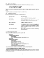
1
DPV 11 serial synchronous
interface user guide
EK-OPV11-UG-OO1
DPV 11 serial synchronous
interface user guide
digital equipment corporation. merrimack, new hampshire
1st Edition, August 1980
Copyright
©
1980 by Digital Equipment Corporation
All Rights Reserved
The material in this manual is for informational purposes and is subject to change without notice.
Digital Equipment Corporation assumes no responsibility for any errors which may appear in this manual.
Printed in U.S.A.
This document was set on DIGITAL·s DECset-8000 computerized
typesetting system.
The following are trademarks of Digital Equipment
Corporation, Maynard, Massachusetts:
DIGITAL
DEC
PDP
DECUS
UNIBUS
DECLAB
o ECsystem -10
DECSYSTEM-20
DIBOL
EduSystem
VAX
VMS
MASSBUS
OMNIBUS
OS/8
RSTS
RSX
lAS
MINC-II
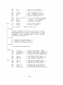
CONTENTS
Page
CHAPTER 1
INTRODUCfION
1.1
1.2
1.3
1.4
1.5
1.5.1
1.5.2
1.5.3
1.6
1.7
SCOPE ....................................... ~ ................................................................................ 1-1
DPVI1 GENERAL DESCRIPTION ...................................................................... 1-1
DPVII OPERATION ............................................................................................... 1-2
DPVl1 FEATURES .................................................................................................. 1-2
GENERAL SPECIFICATIONS ............................................................................. 1-2
Environmental Specifications ............................................................................ 1-2
Electrical Specifications ..................................................................................... 1-3
Performance Parameters .................................................................................... 1-3
DPVII CONFIGURATIONS .................................................................................. 1-3
EIA STANDARDS OVERVIEW ............................................................................ 1-3
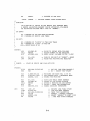
CHAPTER 2
INSTALLATION
2.1
2.2
2.3
2.4
2.4.1
2.4.2
2.5
INTRODUCTION .................................................................................................... 2-1
UNPACKING AND INSPECTION ....................................................................... 2-1
PRE-INSTALLATION REQUIREMENTS .......................................................... 2-1
INSTALLATION ...................................................................................................... 2-6
Verification of Hardware Operation .................................................................. 2-7·
Connection to External Equipment/Link Testing ............................................ 2-8
TEST CONNECTORS ............................................................................................. 2-8
CHAPTER 3
REGISTER DESCRIPTIONS AND PROGRAMMING INFORMATION
3.1
3.2
3.3
3.3.1
3.3.2
3.3.3
3.3.4
3.3.5
3.4
3.4.1
3.4.2
3.5
INTRODUCTION .................................................................................. ~ ................... 3-1
DPV11 REGISTERS AND DEVICE ADDRESSES ............................................. 3-1
REGISTER BIT ASSIGNMENTS ......................................................................... 3-2
Receive Control and Status Register (RXCSR) ............................................... 3-2
Receive Data and Status Register (RDSR) ...................................................... 3-2
Parameter Control Sync/Address Register (PCSAR) ..................................... 3-2
Parameter Control and Character Length Register (PCSCR) ........................ 3-2
Transmit Data and Status Register (TDSR) ..................................................... 3-2
DATA TRANSFERS .............................................................................................. 3-19
Receive Data .................................................................................................... 3-19
Transmit Data .................................................................................................. 3-20
INTERRUPT VECTORS ....................................................................................... 3-21
III
CONTENTS (Cont)
Page
APPENDIX A
DIAGNOSTIC SUPERVISOR SUMl\rIARY
A.I
A.2
A.3
A.5
INTRODUC'TI0N ..................................................................................................
VERSIONS OF THE DIAGNOSTIC SUPERVISOR ........................................
LOADING AND RUNNING A SUPERVISOR DIAGNOSTIC .....................
SUPERVISOR COMMANDS ...............................................................................
Command Switches ..........................................................................................
Control/Escape Characters Supported ...........................................................
THE SE~rUp UTILITY ...........................................................................................
APPENDIX B
USYNRT DESCRIPTION
APPENDIX C
IC DESCRIPTIONS
C.I
C.2
C.3
C.4
C.5
C.6
C.7
C.8
C.9
GENERAL ............................................................................................................
DC003 INTERRUPT CHIP ...................................................................................
DC004 PROTOCOL CHIP .....................................................................................
Dea05 BUS TRANSCEIVER CHIP ....................................................................
26LS32 QUAD DIFFERENTIAL LiNE RECEIVER ........................................
8640 UNIBUS RECEIVER ....................................................................................
8881 Nl\ND ............................................................................................................
9636A DUAL LINE DRIVER ...............................................................................
9638 DUAL DIFFERENTIAL LINE DRIVER ...................................................
APPENDIX D
PROGRAMMING EXAMPLES
A.4
A.4.I
A.4.2
A-I
A-I
A-I
A-3
A-4
A-4
A-5
C-l
C-l
C-3
C-3
C-6
C-6
C-6
C-6
C-6
GLOSSARY
ILLUSTRA TIONS
Figure No.
I-I
2-1
2-2
2-3
2-4
3-1
3-2
3-3
3-4
3-5
3-6
A-I
Title
Page
DPVll System ............................................................................................................ 1-1
DPV 11 Jumper Locations .......................................................................................... 2-4
H3259 Turn-Around Test Connector ......................................................................... 2-8
RS-423-A with H3259 Test Connector ................................................................... 2-10
H3260 On-Board Test Connector ............................................................................. 2-11
DPV 11 Register Configurations and Bit Assignments .............................................. 3-3
Receive Control and Status Register (RXCSR) Format .......................................... 3-4
Receive Data and Status Register (RDSR) Format.. ................................................ 3-8
Parameter Control Sync/Address Register (PCSAR) Format. ......................... " ... 3-11
Parameter Control and Character Length Register
(PCSCR) Format ...................................................................................................... 3-13
Transmit Data and Status Register (TDSR) Format ........ " ................................... 3-17
Typical XXDP+ /Diagnostic Supervisor !'.1emory Layout.. .. " ......... ".""""."."." .. A-2
iv
ILLUSTRATIONS (Cont)
Figure No.
B-1
B-2
C-l
C-2
C-3
C-4
C-S
C-6
C-7
C-8
Title
Page
Terminal Connection Identification Diagram
(2112S17-0-0 Variation) ........................................................................................... B-2
S02S Internal Register Bit Map (2112517-0-0 Variation)....................................... B-3
DC003 Logic Symhol ............................................................................. :................. C-I
DC004 Simplified Logic Diagram .................................................. ~ ........................ C-4
DCOOS Simplified Logic Diagram ........................................................................... C-7
26LS32 Terminal Connection Diagram and Terminal
Indentification ........................................................................................................... C-9
8640 Equivalent Logic Diagram ..............................................................................C-l 0
8881 Pin Identification ............................................................................................C-I 0
9636A Logic Diagram and Terminal Identification ................................................ C-11 .
9638 Logic Diagram and Terminal Identification ................................................... C-12
TABLES
Table
No.
2-1
2-2
2-3
2-4
2-S
3-1
3-2
3-3
3-4
3-S
3-6
C-l
C-2
C-3
Title Page
Page
Configuration Sheet .................................................................................................... 2-1
Vector Address Selection ............................................................................................ 2-S
Device Address Selection ........................................................................................... 2-6
Voltage Requirements ................................................................................................ 2-7
H32S9 Test Connections ............................................................................................. 2-9
DPV II Registers .......................................................................................................... 3-1
Receive Control and Status Register (RXCSR) Bit
Assignments ................................................................................................................ 3-5
Receive Data and Status Register (RDSR) Bit Assignments ................................... 3-8
Parameter Control Sync/ Address Register (PCSAR)
Bit Assignments ......................................................................................................... 3-11
Parameter Control and Character Length Register
(PCSCR) Bit Assignments ....................................................................................... 3-14
Transmit Data and Status Register (TDSR) Bit Assignments ............................... 3-17
DC003 Pin/Signal Descriptions .................................................................................C-2
DC004 Pin/Signal Descriptions .................................................................................C-S
DCOOS Pin/Signal Descriptions .................................................................................C-8
v
PREFACE
This manual is intended to provide an introduction to the DPVll Interface and present the information required by the user for configuration, installation and operation.
It contains the following categories of information.
•
General description including features,specifications, and configurations
•
Installation
•
Programming
The manual also contains four appendixes which include diagnostic information, integrated circuit descriptions, and programming examples.
The DPVll Field Maintenance Print Set (MP00919) contains useful additional information.
VII
CHAPTER 1
INTRODUCfION
1.1 SCOPE
This chapter contains introductory information about the DPVIl. It includes a general description,
and a brief overview of the DPVII operation, features, general specifications, and configurations.
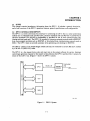
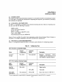
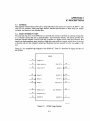
1.2 DPVII GENERAL DESCRIPTION
The DPVII is a serial synchron.ous line interface for connecting an LSI-II bus to a serial synchronous
modem that is compatible with EIA RS-232-C interface standards and EIA RS-423-A and RS-422-A
electrical standards. EIA RS-422-A compatibility is provided for use in local communications only
(timing and data leads only). The DPVll is intended for character-oriented protocols such as BISYNC,
byte count-orieated protocols such as DDCMP, or bit-oriented data communication protocols such as
SDLC. The DPVII does not provide automatic error generating and checking for BISYNC.
The DPVll consists of one double-height module and may be connected to an EIA RS-232-C modem
by a BC26L-25 (RS-232-C) cable.
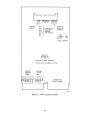
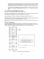
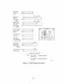
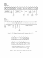
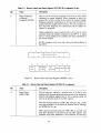
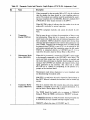
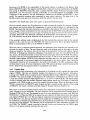
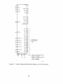
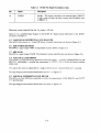
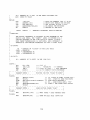
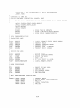
The DPVII is a bus request device only and must rely on the system software for service. Interrupt
control logic generates requests for the transfer of data between the DPVll and the LSI-II memory by
means of the LSI-II bus. (Figure 1-1 shows the DPVII system.)
DPV11
BC26l-25
RS-232 - C
MODEM
TELEPHONE
L1 N E
_ _-..,.
t - -_
en
:::>
co
I
en
.....I
CPU
MEM
MK·1320
Figure 1-1
DPVII System
1-1
1.3 DPVIIOPERATION
The DPV 11 is a double-buffered program interrupt interface that provides parallel-to-serial conversion
of data to be transmitted and serial-ta-parallel conversion of received data. The DPV II can operate at
speeds up to 56K b/s. * It has five 16-bit registers which can be accessed in word or byte mode. These
registers are assigned a block of four contiguous LSI-II bus word addresses that start on a boundary
with the low-order three bits being zeros. This block of addresses is jumper-selectable and may be
located anywhere between 1600008 and 1777768. Two of these registers share the same address. One is
accessed during a read from the address, the other during a write to the address. For a detailed description of each of the five registers, refer to Chapter 3. These registers are used for status and control
information as well as data buffers for both the transmitter and receiver portions of the DPV 11.
1.4
DPVII FEATURES
Features of the DPVII include:
•
Full-duplex or half-duplex operation
•
Double-buffered transmitter and receiver
•
EIA RS-232-C compatibility
•
All EIA RS-449 Category I modem control
•
Partial Category Ii modem control to indude incoming cali, test mode, remote loopback,
and localloopback
•
Program interrupt on transitions of modem control signals
•
Operating speeds up to 56K bls (may be limited by software or CPU memory)
•
Software-selectable diagnostic loopback
•
Operation with bit-, byte count-, or character-oriented protocols
•
Internal cyclic redundancy check (CRC) character generation and checking (not usable
with BISYNC)
.
•
Internal bit-stuff and detection with bit-oriented protocols.
•
Programmable sync character, sync insertion, and sync stripping with byte count-oriented
protocols.
•
Recognition of secondary station address with bit-oriented protocols.
1.5 GENERAL SPECIFICATIONS
This paragraph contains environmental, electrical, and performance specifications for the DPVII.
1.5.1
Environmental Specifications
The DPV II is designed to operate in a Class C environment as specified by DEC Standard 102 (extended).
50 C (41 0 F) to 60 0 C (140 0 F)
Operating Temperature
Relative Humidity
10% to 90% with a max. wet bulb temperature of 28 0 C (82 0
F) and a min. dew point of 2 0 C (36 0 F)
• The actual speed realized may be significantly less because of limitations imposed by the software and/or CPU memory
refresh.
1-2
1.5.2 Electrical Specifications
The DPV 11 requires the following voltages from the LSI-II bus for proper operation.
+ 12 V at 0.30 A max. (0.15 A typical)
+ 5 V at 1.2 A max. (0.92 A typical)
The interface includes a charge pump to generate a negative voltage required to power the RS-423-A
drivers.
The DPVII presents 1 ac load and 1 dc load to the LSI-II bus.
1.5.3 Performance Parameters
Performance parameters for the DPVII are listed as follows.
Operating Mode
Full or half-duplex
Data Format
Synchronous BISYNC, DDCMP, and SDLC
Character Size
Program-selectable (5-8 bits with character-oriented
protocols and 1-8 bits with bit-oriented protocols)
Max. Configuration
16 DPVII modules per LSI-II bus
Max. Distance
15 m (50 ft) for RS-232-C. 61 m (200 ft) for RS-423AjRS-422-A (Distance is directly dependent on speed,
and 200 ft is a suggested average. See RS-449 specification for details.)
Max. Serial Data Rates
56K bjs (May be less because" of software and memory
refresh limitations.)
1.6 DPVll CONFIGURATIONS
There are two DPVII configurations, the DA and the DB.
DPVII-DA
Unbundled version consists of:
M8020 module
DPVII Maintenance Reference Card (EK-DPVII-CG)
DPVII-DB
Bundled version consists of:
M8020 module
H3259 turn-around connector
BC26L-25 cable
DPVII User Manual (EK-DPVII-UG)
DPVII Maintenance Reference Card (EK-DPVII-CG)
LIB kit (ZJ3I4-RB)
Field Maintenance Print Set (MP009I9)
Turn-around connectors, cables and documentation may be purchased separately.
1.7 EIA STANDARDS OVERVIEW (RS-449jRS-232-C)
The most common interface standard used in recent years has been the RS-232-C. However, this standard has serious limitations for use in modern data communication systems. The most critical limitations
are in speed and distance.
1-3
For this reason, RS-449 standard has been developed to replace RS-232-C; It maintains a degree of
compatibility with RS-232-C to accommodate an upward transition to RS-449.
The most significant difference between RS-232-C and RS-449 is in the electrical characteristics of
signals used between the data communication equipment (DCE) and the data terminal equipment
(DTE). The RS-232-C standard uses only unbalanced circuits, while the RS-449 uses both balanced
and unbalanced electrical circuits. The specifications for the types of electrical circuits supported by
RS-449 are contained in EIA standards RS-422-A for balanced circuits and RS-423-A for unbalanced
circuits. These new standards permit much greater transmission speed and will allow greater distance
between DTE and DCE. The maximum transmission speeds supported by RS-422-A and RS-423-A
circuits vary with cable length; the normal speed limits are 20K bls for RS-423-A and 2M bls for RS422-A, both at 61 m (200 feet).
Another major difference between RS-232-C and RS-449 is that additional leads are needed to support
the balanced interface circuits and some new circuit functions. Two new connectors have been specified
to accommodate these new leads. One connector is a 37-pin Cinch used in applications requiring secondary channel functions. Some of the new circuits added in RS-449 support local and remote loopback
testing, and stand-by channel selection.
1-4
CHAPTER 2
INSTALLATION
2.1 INTRODUCTION
This chapter provides all the information necessary for a successful installation and subsequent checkout of the DPV 11. Included are instructions for unpacking and inspection, pre-installation, installation
and verification of operation.
2.2 UNPACKING AND INSPECfION
The DPVl1 is packaged in accordance with commercial packing practices. Remove all packing material and verify that the following are present.
M8020 module
H3259 turn-around connector
BC26L-25 cable
DPVll User Manual (EK-DPVII-UG)
LIB kit (ZJ314-RB)
Field Maintenance Print Set (MP009I9)
Inspect all parts carefully for cracks, loose components or other obvious damage. Report damages or
shortages to the shipper immediately, and notify the DIGITAL representative.
2.3 PRE-INSTALLATION REQUIREMENTS
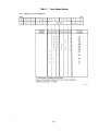
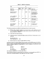
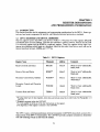
Table 2-1 (Configuration Sheet) provides a convenient, quick reference for configuring jumpers.
Table 2-1
Configuration Sheet
(WI-W2) Driver Attenuation Jumper
Driver
Terminal
Timing
Normal*
Configuration
Alternate *
Option
WI to W2
Not connected
Description
Bypasses
resistor.
attenuation
Jumper must be removed forcertain modems to operate properly.
(W 3-W 11) Interface Selection Jumpers
Input
Signals
Normal*
Configuration
SQ/TM
(PCSCR-5)
W5toW6
DM (DSR)
(RXCSR-9)
Not connected
Alternate *
Option
Description
Signal quality
W7toW6
Test mode
WIO to W9
Data mode return for RS-422-A
*Normal configuration is typically RS-423-A compatible. Alternate option is typically RS-422-A compatible.
2-1
Table 2-1
Configuration Sheet (Cont)
(W3-Wtl) Interface Selection Jumpers (Cont)
Output
Signals
Normal*
Configuration
SF/RL
(RXCSR-O)
W3 to W4
local
loopback
Alternate *
Option
Description
Select frequency
W5 to W3
Remote loopback
W8 to W9
Not connected
localloopback
Not connected
W8 to WII
Localloopback (alternate pin)
Description
(WI2-WI7) Receiver' Termination Jumpers
Receiver
Normal*
Configura tion
Alternate*
Option
Receive Data
Not connected
WI2 to WI3
Send Timing
Not connected
W14 to W15
Receive
Timing
Not connected
WI6 to WI7
Connects terminating resistor for
RS-422-A compatibility
-
(WlS-W23) Clock Jumpers
Function
Normal*
Configuration
NUll MODEM
W20 to WI8
Alternate*
Option
Description
Sets NUll elK MODEM elK
to 2 kHz.
(;LK
Clock Enable
WI9 to W2I
W22 to W23
W21 to WI8
Sets NUll MODEM elK to
50 kHz.
W19 to W21
W22 to W23
Always installed except for factory
testing.
Description
(W24-W2S) Data Set Change Jumpers
Modem Signal
Name
Normal*
Configuration
Alternate*
Option
Data Mode (DSR)
W26 to W24
Not connected
Clear to Send
W26 to W25
Not connected
Incoming Call
W26 to W27
Not connected
Receiver Ready
(Carrier Detect)
W26 to W28
Not connected
*Normal configuration is typically RS-423-A compatible.
Al~~2ate
Connects the DSCNG flip-flop to
the respective modem status signal
for transition detection.
Note: W26 is input to DSCNG flipflop
option is typically RS-422-A compatible.
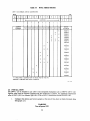
Table 2-1
Configuration Sheet (Cont)
De~ice
GND AI2
W29 W3l
All
W30
AIO
W36
Address Jumpers
A9
W33
A8
W32
A7
W39
A6
W38
A5
W37
A4
W34
A3
W35
NOTE
The address to which the DPVll is to respond is
daisy-chain jumpered to W29 (GND).
Vector Address Jumpers
D8
W43
D7
W42
D6
W41
D5
W40
D4
W44
D3
W45
Source
W46
NOTE
Vector address to be asserted is daisy-chain jumpered to W46.
NOTE
Table 2-1 shows the recommended normal and alternate jumpering schemes. Any deviation from these
will cause diagnostics to fail and require restrapping
for full testing and verification. It is recommended
that customer configurations that vary from this
scheme not be contractually supported.
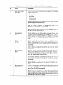
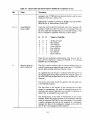
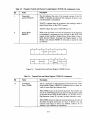
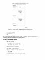
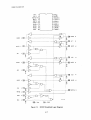
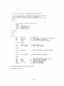
Prior to installing the DPV 11, perform the following tasks.
1.
Verify that the following modem interface wire-wrap jumpers are installed (Figure 2-1).
W26 to W25 to W24 to W28 to W27
W22 to W23 and WI9 to W2I
WI8 to W20
W5 to W6
W3 to W4
W8 to W9
WI to W2
This is the normal/RS-423-A shipped configuration. Some of these jumpers may be changed
. when the module is connected to external equipment for a specific application. The NULL
MODEM eLK is set to 2 kHz as shipped.
2.
Based on the LSI-II bus floating vector scheme or user requirements, determine the vector
address for the specific DPVII module being installed and configure W40 through W46
accordingly (Table 2-2).
3.
Based on the LSI-II bus floating address scheme or user requirements, determine the device
address range for the DPVll module and configure W30 through W39 accordingly (Table
2-3). Devices may be physically addressed starting at 160000 and continuing through
177776; however, there may be some software restrictions. The normal addressing convention is as shown in Table 2-3.
2-3
c
J
J1
CYO<YOO
CJO
W1 2
0'000
34567891011
\....-.v--.J
"--.,;---J
TERMINAL /
012 ......
TIMING
013
TERMINATING
RESISTOR
0 14
JUMPERS
015 ( FOR RS-422-A
016
017 )
" " iNTERFACE
SELECTION
JUMPERS
19
21
22
000b
~
W18 20
23
CLOCK JUMPERS
25
27
~
24
26* 28
DATA SET CHANGE JUMPERS
*W26 IS INPUT TO DSCNG FLIP FLOP
SHIPPED
ADDRESS
SHIPPED
VECTOR
160010
300
~~
W2930 3234 36 38
.00 0000
..: 00 0 0 0
31 3335 3739
40 42 44 46
00 0 0
00
0
41 43 45
JUMPERS ARE
DAISY CHAINED
~
8
A
MK·1338
Figure 2-1
DPV11 Jumper Locations
2-4
Table 2-2
Vector Address Selection
DPVll (M8020) VECTOR ADDRESSING
MSB
I
15
14
13
12
11
10
9
0
0
0
0
0
0
0
1
l
8
I 7
1 6
5
t 4
I
3
JUMPERS
2
1
0
1/0
0
·0
I
I
I
I
I
I
JUMPER
NUMBER
1
LSB
W43 W42 W41 W40 W44 W45
X
X
X
X
X
X
X
X
X
X
X
X
X
X
X
X
X
X
X
X
X
X
X
X
X
X
X
X
X
VECTOR
ADDRESS
300
310
320
330
340
350
360
370
400
--X
X
500
--X
X
X
X
600
--X
700
---
"X" INDICATES A CONNECTION TO W46.
W46 IS THE SOURCE JUMPER FOR THE VECTOR ADDRESS
JUMPERS ARE DAISY CHAINED.
MK 1341
2-5
Table 2-3
Device Address Selection
DPV11-XX (M8020) DEVICE ADDRESSING
MSB
15
14
13
1
1
1
12 111 1 10
,
.
J9
•
I
W31
8
1
7
1
6
1 I 1
5
4
JUMPERS
I
I
I
I
I
I
I
JUMPER
NUMBER
1
LSB
3
~
I
I
I
I
I
I
I
I
I
I
W30 W36 W33 W32 W39 W38 W37 W34 W35
X
X
X
X
X
X
X
X
X
X
X
X
X
I
I
2
1
0
0
0
0
DEVICE
ADDRESS
760010
760020
760030
760040
760050
760060
760070
760100
--760200
X
--X
X
760300
-- 760400
X
--X
X
760500
--X
X
X
X
760600
-- X
760700
--761000
X
--762000
X
--X
763000
X
---
X
764000
"X" INDICATES A CONNECTION TO W29. W29 IS TIED TO
GROUND. JUMPERS ARE DAISY CHAINED.
MK1339
2.4 INSTALLATION
The DPVII can be installed in any LSI-II bus-compatible backplane such as H9270. LSI-II configuring rules must be followed. Proceed with the installation as follows. For additional information
refer to PDP-II/03 User Manual ~!<-LSIII-TM or LSI-II Installation Guide EK-LSIII-IG.
1.
Configure the address and vector jumpers at this time if they have not been previously done
(Paragraph 2.3).
WARNING
Turn all power OFF.
2-6
2.
Connect the female Berg connector on the BC26L-25 cable to J 1 on the M8020 module t
and plug the module into a dual LSI-II bus slot of the backplane.
CAUTION
Insert and remove modules slowly and carefully to
avoid snagging module components on the card
guides.
3.
Connect the H3259t turn-around connector to the EIA connection on the BC26L-25 cable.
The jumper WI on the H3259 turn-around connector must be removed.
4.
Perform resistance checks from backplane pin AA2 (+ 5 Y) to ground and from AD2 (+ 12
Y) to ground to ensure that there are no shorts on the M8020 module or backplane.
5.
Turn system power on.
6.
Check the voltages to ensure that they are within the specified tolerances (Table 2-4). If
voltages are not within specified tolerances, replace the associated regulator (H780 P.S.)
Table 2-4
Voltage Requirements
Voltage
Max.
Min.
Backplane Pin
+5V
+I2Y
+5.25
12.75
+4.75
+ 11.25
AA2
AD2
2.4.1 Verification of Hardware Operation
The M8020 module is now ready to be tested by running the CYDPY* diagnostic. Additional information on the DPVII diagnostics is contained in Appendix A. Proceed as follows.
NOTE
The • represents the revision level of the diagnostic.
1.
Load and run CVDPV·. Three consecutive error-free passes of this test is the minimum requirement for a successful run. If this cannot be achieved, check the following.
Board seating
Jumper connections
Cable connection
Test connector
If a successful run is still unachievable, corrective maintenance is required.
2.
Load and run the DEC/XII System Exerciser configured to test the number of DPYlis in
the system.
Each DEC/XII CXDPV module will test up to eight consecutively addressed DPYlls.
CXDPY uses a software switch register. Refer to the DEC/Xii Cross-Reference (ASF055e-MC) for switch register utilization.
t If a BC26L-25 cable and H3259 tum-around connector are not available, an on-board test connector (H3260) can be ordered separately. See Paragraph 2.5.
2-7
The DEC/X 11 System Exerciser is designed to achieve maximum contention with all devices that make up the system configuration. It is within this environment that the CXDPY
module runs. Its intent is to isolate DPY 11 s which adversely affect the system operation.
For information on configuring and running the DEC/X 11 System Exerciser, refer to
DEC/X}} User Manual (AS-F0503B-MC) and DEC-X}} Cross Reference (AS-F055CMC).
2.4.2
Connection to External Equipment/Link Testing
The DPY 11 is now ready for connection to external equipment.
If the DPY 11 is being connected to a synchronous modem, remove the H3259 connector and install the
EIA connection of the BC26L-25 cable into the connector on the modem.
Configure jumpers WI-W28 in accordance with operating requirements (Table 2-1).
Load and run DCLT (CYCLH*) if a full link is available. This will check the final configuration and
isolate failures to the CPU, the communications link, or the modem.
If the connection to external equipment uses RS-422-A, the user must provide the cable and test support.
2.5
TEST CONNECfORS
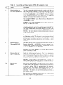
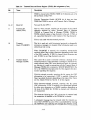
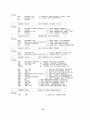
The only test connector provided with the DPY 11 is the H3259 turn-around connector (Figure 2-2).
Table 2-5 and Figure 2-3 show the relationship between pin numbers, signal names and register bits
when the H3259 is connected by means of the BC26L-26 cable to the M8020 module.
24 ••~___N_U_LL_M_O_D_E_M~__
TCP
15 __. - - - - - - - - - - - - - .
RCP
17 __4---~--------~----~_
11 __----S-EC-X-M-IT---_~----.............J WI·
14 __- - - - - - - - - - - -__
19 __- - - - - - - - - - - - - _
SELECT FREO
23 __----~----+-.
12 __- - - - - - - - - - - - .
SEC REC
16--.-----------REMOTE LOOP
21 . .---(~SI~G~NA~L~O~U~A~LlT=Y~)·
25~-------------TEST MODE
XMIT DATA
11
WI·
23=-_
__
____
_
REC
DATA
_
:: :
18:
6
.!
RTS
CTS
RR
•••••••• •• •• •
•••••••••• ••
o
H 3259
LOCAL LOOP
..
o
0------.
DATA MODE
DTR
INCOMING CALL-
I
I
. WI IS CUT FOR TESTING DPV 11
MK 1329
Figure 2-2
H3259 Turn-Around Test Connector
2-8
Table 2-5 "3259 Test Connections
To
From
Signal Name
Pin No.
H3259
Pin No.
J1
Pin No.
Jl
Pin No.
H3259
Signal Name
SEND DATA
2
F
J
3
RECEIVE DATA
REQUEST TO SEND
(RTS) (RXCSR-2)
4
V
BB&T
5&8
CLEAR TO SEND
(CTS)(RXCSR-13),
RECEIVER READY
(RR) (RXCSR-12)
LOCAL LOOPBACK
(LL) (RXCSR-3)
18
U
Z
6
DATA MODE
(DM) (RXCSR-9)
RR/MM
MM/C
21/25
SIGNAL QUALITY /
TEST MODE
(SQ/TM) (PCSCR-5)
SELECTFREQ/REMOTE 23/21
LOOPBACK
(SF /RL) (RXCSR-O)
NULL MODEM
24
L
N&R
15&17
RCV CLOCK
TXCLOCK
DATA TERMINAL
READY (DTR)
(RXCSR-l)
20
DO
X
22
INCOMING CALL
(lC) (RXCSR-14)
The following accessories are available for interfacing and may be ordered separately.
•
BC26L-X cable. Available in lengths of .3, 1.8, 2.4, 3.0, 3.6,6.1, and 7.6 meters (1, 6,8, 10,
12, 20 and 25 feet). When ordering, the dash number indicates the desired cable length in
feet; e.g., BC26L-25 or BC26L-l.
•
H3259 cable turn-around connector
•
H856 Berg connector. Includes H856 Berg connector and 40 pins. Crimping tools are available from:
Berg Electronics, Inc.
New Cumberland, PA
•
17070
H3260 on-board test connector (includes RS-422-A testing)
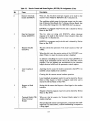
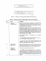
The H3260 on-board test connector (Figure 2-4) may be used to test the M8020 circuitry in its entirety.
RS-422-A circuitry is not tested with the H3259 cable turn-around connector. The H3260 on-board test
connector is shipped configured for testing RS-422-A. It may be configured to test RS-422-A or RS423-A as follows.
RS-422-A
RS-423-A
WI-W2 installed
Wl-W2 out
W3-W6 out
W3-W6 installed
The connector is installed into Jl with the jumper side up.
Since the H3260 on-board test connector does not test the cable, it is recommended that the DPVII be
tested with a turn-around connector at the modem end of the cable if possible.
2-9
3~6
SEND DATA
E40
~
RECEIVE DATA
TX CLOCK
TCP
.....,
3
E38
H3259
F
2
J
3/
5
·
·
H
~10
15
TY
n
E38
R
~~
2~7
LOCAL CLK
J1
I
~~
8
rV
2
5~7
RCV CLOCK
RCP
~
17)
· (
SS
L
I
16
NN
/
P
SO/TM
PCSCR 5
W7
8?14
13
E25
I
3
~~
If'')
vJ
READY
~7
'
W10
W8
W9
W11
14
K
I
X
22
~10
'\
:z~
20..../
RXCSR 14 (INCOMING 11
CAlli
RSCSR·1 (oTR)
REQUEST TO SEND
RXCSR 12 (RRJ
RECEIVER READY
.
P
VV
I
T
13
CLEAR TO SEND
2
~
r~
~~
9
10
W
l~14
RSCSR·13 (CTS)
RSCSR·2IRTSI
Y
3~6
DATA TERMINAL
READY
",,11 J
15
r--
V
J
7
·
BB
1
M
3~
THIS JUMPER
MUST BE
J REMOVED WHEN
TESTING A DPV11
~18
LL
-- -
I
6
U
---
I
2y I
!
·
I
-~
LOCAL LOOP BACK
FF
PP
J:::~7 i
RXCSR-3 (LL)
12/
RR
1
1
W
\21
JJ
/
W4
5~6
DATA SET
/
/
MM
W6/ W5
~;/
,,'\.25
PP
1
15
f---
SF/RL
RXCSRO
I'
C
I
.
13
1
5
i
~8
E
M
~2-
.·
.·
·
NEGATIVE INPUT TO DIFFERENTIAL
RECEIVERS OMITTED FOR CLARITY
~
~
MK l:nfi
Figure 2-3
RS-423-A with H3259 Test Connector
2-10
TEST MODE
SIGN QUAL
SF/Rl
SEND DATA
RX DATA
SEND DATA
(RS422)
TERM TIMING
SEND TIMING
RX TIMING
TERM TIMING
(RS422)
CLEAR TO SEND
REQ TO SEND
RX ROY
INCOMING CAll
TERM ROY
DATA MODE
DATA MODE RET
(lOCAL lOOP)
MR~~
Wl
W3
Fe_ _ _ _ _-d--'~
A~~
-------.--n
W2
W4
le
;:
B~:
o
t
o
5013970A
RS422
W6~
RS423
D~:
~:
:J
W5
SEND TIM RET
RX TIM RET
TERM TIM RET
(RS422)
______J
E~
W6
SEND DATA RET
RX DATA RET
~
K~:
H3260 TEST CONNECTOR
NOTE: 1. Wl & W2 IN
W3-W6 OUT
2. Wl & W2 OUT
W3-W6 IN
RS-423-A TESTING
RS-422-A TESTI NG
MK1464
Figure 2-4
H3260 On-Board Test Connector
2-11
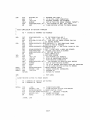
CHAPTER 3
REGISTER DESCRIPTIONS
AND PROGRAMMING INFORMATION
3.1 INTRODUCTION
This chapter describes the bit assignments and programming considerations for the DPVll. Some typical start and receive sequences for both bit- and character-oriented protocols are included.
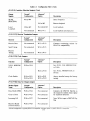
3.2 DPVll REGISTERS AND DEVICE ADDRESSFS
The five registers used in the DPVll are shown in Table 3-1. Note that two of the registers (PCSAR
and RDSR) have the same address. This does not constitute a conflict, however, because the PCSAR
is a write-only register and the RDSR is a read-only register. These five registers occupy eight contiguous byte addresses which begin on a boundary where the low-order three bits are zero, and can be
located anywhere between 1600008 and 1777768.
Table 3-1
DPVll Registers
Register Name
Mnemonic
Address
Comments
Receive Control and Status
RXCSR
16xxxO
Word or byte* addressable.
Read/write.
Receive Data and Status
RDSR**
16xxx2
Word or byte* addressable.
Read-only.
Parameter Control Sync/Address
PCSAR**
16xxx2
Word or byte addressable.
Write-only.t
Parameter Control and Character
Length
PCSCR+
16xxx4
Word or byte addressable.
Read/write.
Transmit Data and Status
TDSR**
16xxx6
Word or byte addressable.
Read/write.
* Reading either byte of these registers, clears data and certain status bits in other bytes. See Paragraphs
3.3.1
and 3.3.2.
** Registers contained within the USYNRT.
t It is not possible to do bit set or bit clear instructions on this register.
+The high byte of this register is internal to the USYNRT.
The DPVll uses a universal-synchronous receiver/transmitter (USYNRT) chip which accounts for a
large portion of the DPVll 's functionality. The USYNRT provides complete serialization, deserialization and buffering of data to and from the modem.
3-1
Most of the DPVll registers are internal to the USYNRT. Only the receiver control and status register (RXCSR) and the low byte of the parameter control and character length register (PCSCR) are
external.
NOTE
When using the special space sequence function, all
registers internal to the USYNRT must be written
in byte mode.
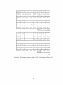
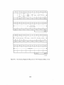
3.3 REGISTER BIT ASSIGNMENTS
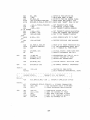
Bit assignments for the five DPV 11 registers are shown in Figure 3-l. Paragraphs 3.3.1-3.3.5 provide a
description of each register using a bit assignment illustration and an accompanying table with a detailed description of each bit.
3.3.1 Receive Control and Status Register (RXCSR) (Address 16xxxO)
Figure 3-2 shows the format for the receive control and status register (RXCSR). Table 3-2 is a detailed description of the register. This register is external to the USYNRT.
NOTE
The RXCSR can be read in either word or byte
mode. However, reading either byte resets certain
status bits in both bytes.
3.3.2 Receive Data and Status Register (RDSR) (Address 16xxx2)
Figure 3-3 show the format for the receive data and status register (RDSR). It is a read-only register
and shares its address with the parameter control sync/address register (PCSAR) which is write-only.
Table 3-3 is a detailed description of the RDSR.
NOTE
The RDSR can be read in either word or byte mode.
However, reading either byte resets data and certain
status bits in botb bytes of tbis register as well as
bits 7 and 10 of the RXCSR.
3.3.3 Parameter Control Sync/Address Register (PCSAR) (Address 16xxx2)
The parameter control sync/address register (PCSAR) is a write-only register which can be written in
either byte or word mode. Figure 3-4 shows the format and Table 3-4 is a detailed description of the
PCSAR. This register shares its address with the RDSR.
NOTE
Bit set (BIS) and bit clear (BIC) instructions cannot be executed on the PCSCR, since they execute
using a read-modify-write sequence.
3.3.4 Parameter Control and Character Length Register (PCSCR) (Address 16xxx4)
The parameter control and character length register (PCSCR) can be read from or written into in
either word or byte mode. The low byte of this register is external to the USYNRT and the high byte is
internal. Figure 3-5 shows the format and Table 3-5 is a detailed description of the PCSCR.
3.3.5 Transmit Data and Status Register (TDSR) (Address 16xxx6)
The format for the transmit data and status register (TDSR) is shown in Figure 3-6 and Table 3-6 is a
detailed description. The TDSR is a read/write register which can be accessed in either word or byte
mode with no restrictions. All bits can be read from or written into and are reset by Device Reset or
Bus INIT except where noted.
3-2
RXCSR
16XXXO
READ/WRITE
15
14
13
12
11
10
09
08
07
06
05
04
03
02
01
00
R
R
R
R
R
R
R
R
R
R/W
RIW
R/W
R/W
R/W
R/W
RIW
I
I
I
I
DATA
SET
CHANGE
CLR
RCV
ACTIVE
DATA
MOVE
10
I
RCV
DATA
READY
SEND
INCOMING
CALL
RCVR
STATUS
READY
RCVR
READY
.I
I
DATA
SET
INTR
EN
SYNC
OR
FLAG
DETECT
I
LOCAL
(LL)
LOOP
RCV
INTR
EN
DATA
TERM
ROY
REQ
TO
SEND
RX
ENA
SF/RL
RDSR
16XXX2
MK·1504
READ ONLY
14
15
12
13
11
09
10
07
08
A~SEMB~ED
00
I
I
I
I
I
I
I
I
I
I
RECEIVE DATA BUFFER
BIT COUNT
I
I
I
I
I
I
I
I
RCVR
OVER
ERROR
CHECK
I
END
OF
MESG
RUN
RCV
ABORT
START
OF
MESG
PCSAR
MK·1505
16XXX2
WRITE ONLY
15
13
14
11
12
08
09
10
00
07
I
ERROR DETECTION
SELECTION
,
I
I
ALL
PARTIES
AODR
I
+
SECONDARY STATION
~
I
1
i
I
I
L
I
I
RECEIVER SYNC
J
~
~
I
STRIP
SYNC OR
LOOP
MODE
PROTOCOL
SELECT
I
IDLE
MODE
SELECT
SECD
ADRS
MODE
SEL
MK·1506
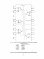
Figure 3-1
DPVll Register Configurations and Bit Assignments (Sheet 1 of 2)
3-3
PCSCR
16XXX4
READ/WRITE
14
15
R/W
RIW
1a
11
R/W
R/W
I
,
12
13
R/W
R/W
R
RIW
04
03
02
01
00
R/W
R/W
RIW
R
R
W
I
I
y
I
I
SQ/TM
RECEIVER
RSVD
CHARACTER LENGTH
EXTD
ADDR
FIELD
TRANSMITTER
CHARACTER LENGTH
05
I
I
,
I
I
y
06
07
08
I
R/W
RIW
I
09
,
I
I
XMIT
INTR
EN
EXTD
CONT
FIELD
I
MAINT
MODE
SELECT
XMTR
ACTIVE
DEVICE
RESET
XMTR
BUFFER
EMPTY
XMTR
ENAB
MK-1507
TDSR
16XXX6
READ/WRITE
14
15
XMI1
DATA
LATE
,
11
12
13
10
09
07
08
0
R/W
R/W
R/W
R/W
R/W
I
I
Y
RESERVED
I
ABORT
R/W
R/W
I
I
R/W
i
.1
R/W
i
\
I
I
R/W
1
R/W
R/W
1
y
i
I
TRANSMIT DATA BUFFER
END
OF
MESG
XMIT
GO
AHEAD
I
I
.1
I
I
00
I
I
0
0
R
I
,
START
OF
MESG
MK-1508
Figure 3-1
DPVll Register Configurations and Bit Assignments (Sheet 2 of 2)
5
4
RX
OS
RX
ITEN
ITEN
ENA
13
12
7
6
RDAT
RY··
15
14
3
2
LL
RTS
11
10
o
TR
SF/RL
9
8
OM
SFD
OS'
CNG
THIS BIT IS RESET BY READING EITHER BYTE OF THIS REGISTER_
.. THESE BITS ARE RESET BY READING EITHER BYTE OF RSDR
MK 1327
Figure 3-2 Receive Control and Status Register (RXCSR) Format
3-4
Table 3-2
Receive Control and Status Register (RXCSR) Bit Assignments
Bit
Name
Description
15
Data Set Change
(DSCNG)
This bit is set when a transition occurs on any of the following
modem control lines:
Clear to Send
Data Mode
Receiver Ready
Incoming Call
Transition detectors for each of these four lines can be disabled
by removing the associated jumper.
Data Set Change is cleared by reading either byte of the
RXCSR or by Device Reset or Bus INIT.
Data Set Change causes a receive interrupt if DSITEN (bit 5)
and RXITEN (bit 6) are both set.
14
Incoming Call
(lC)
)'his bit reflects the state of the modem Incoming Call line. Any
transition of this bit causes Data Set Change bit (bit 15) to be
asserted unless the Incoming Call line is disabled by removing
its jumper. This bit is read-only and cannot be cleared by software.
13
Clear to Send
(CTS)
This bit reflects the state of the Clear to Send line of the
modem. Any transition of this line causes Data Set Change (bit
15) to be set unless the jumper enabling the Clear to Send signal
is removed.
Clear to Send is a program read-only bit and cannot be cleared
by software.
12
Receiver Ready
(RR)
This bit is a direct reflection of modem Receiver Ready lead. It
indicates that the modem is receiving a carrier signal. For external maintenance loop back, this signal must be high. If the line is
open, RR is pulled high by the circuitry.
Any transition of this bit ,causes Data Set Change (bit 15) to be
asserted unless the jumper enabling the Receiver Ready signal
is removed.
Receiver Ready is a read-only bit and cannot be cleared by software.
11
Receiver Active
(RXACT)
This bit is set when the USYNRT presents the first character of
a message to the DPVIl. It remains set until the receive data
path of the USYNRT becomes idle.
Receiver Active is cleared by any of the following conditions: a
terminating control character is received in bit-oriented protocol
mode; an off transition of Receiver Enable (RXENA) occurs; or
Device Reset or Bus INIT is issued.
3-5
Table 3-2
Bit
Receive Control and Status Register (RXCSR) Bit Assignments (Cont)
Name
Description
Receiver Active is a read-only bit which reflects the state of the
USYNRT output pin 5.
10
Receiver Status
Ready (RSTARY)
This bit indicates the availability of status information in the
upper byte of the receive data and status register (RDSR). It is
set when any of the following bits of the RDSR are set: Receiver
End of Message (REOM); Receiver Overrun (RCV OVRUN);
Receiver Abort or Go Ahead (RABORT); Error Check
(ERRCHK) if VRC is selected.
Receiver Status is cleared by any of the following conditions:
reading either byte of the RDSR; clearing Receiver Enable (bit
4 of RXCSR); Device Reset, or Bus Init.
When set, Receiver Status Ready causes a receive interrupt if
Receive Interrupt Enable (bit 6) is also set.
Receiver Status Ready is a read-only bit which reflects the state
of USYNRT pin 7.
9
Data Mode (DM)
(Data Set Ready)
This bit reflects the state of the Data Mode signal from the
modem.
When this bit is set it indicates that the modem is powered on
and not in test, talk or dial mode.
Any transition of this bit causes the Data Set Change bit (bit
15) to be asserted unless the Data Mode jumper has been removed.
Data Mode is a read-only"bit and cannot be cleared by software.
8
Sync or Flag
Detect (SFD)
This bit is set for one clock time when a flag character is detected with bit-oriented protocols, or a sync character is detected with character-oriented protocols.
SFD is a read-only bit which reflects the state of USYNRT pin
4.
7
Receive Data
Ready (RDA TRY)
This bit indicates that the USYNRT has assembled a data character and is ready to present it to the processor.
If this bit becomes set while Receiver Interrupt Enable (bit 6) is
set, a receive interrupt request will result.
Receive Data Ready is reset when either byte of RDSR is read,
Receiver Enable (bit 4) is cleared, or Device Reset or Bus INIT
is issued.
RDATRY is a read-only bit which reflectes the state of USYNRT pin 6.
3-6
Table 3-2
Receive Control and Status Register (RXCSR) Bit Assignments (Cont)
Bit
Name
Description
6
Receiver Interrupt
Enable (RXITEN)
When set, this bit allows interrupt requests to be made to the
receiver vector whenever RDATR Y (bit 7) becomes set.
The conditions which cause the interrupt request are the assertion of Receive Data Ready (bit 7), Receive Status Ready (bit
10), or Data Set Change (bit 15) if DSITEN (bit 5) is also set.
RXITEN is a program read/write bit and is cleared by Device
Reset or Bus INIT.
5
Data Set Interrupt
Enable (DSITEN)
This bit, when set along with RXITEN, allows interrupt
requests to be made to the receiver vector whenever Data Set
Change (bit 15) becomes set.
DSITEN is a program read/write bit and is cleared by Device
Reset or Bus INIT.
4
Receiver Enable
(RXENA)
This bit controls the operation of the receive section of the USYNRT.
When this bit is set, the receive section of the USYNRT is enabled. When it is reset the receive section is disabled.
In addition to disabling the receive section of the USYNRT, resetting bit 4 reinitializes all but two of the USYNRT receive
registers. The two registers not reinitialized are the character
length selection buffer and the parameter control register.
3
Local Loopback
(LL)
Asserting this bit causes the modem connected to the DPVll to
establish a data loopback test condition.
Clearing this bit restores normal modem operation.
Local Loopback is program read/write and is cleared by Device
Reset or Bus request to Send is program read/write and is
cleared by Device Reset or Bus INIT.
2
Request to Send
(RTS)
Setting this bit asserts the Request to Send signal at the modem
interface.
Request to Send is program read/write and is cleared by Device
Reset or Bus INIT.
Terminal Ready (TR)
(Data Terminal
Ready)
When set, this bit asserts the Terminal Ready signal to the
modem interface.
For auto dial and manual call origination, it maintains the established call. For auto answer t it allows handshaking in response to
a Ring signal.
3-7
Table 3-2
Receive Control and Status Register (RXCSR) Bit Assignments (Cont)
Bit
Name
Description
o
Select Frequency
or Remote
Loopback (SF /RL)
This bit can be wire-wrap jumpered to function as either select
frequency or remote loopback. When jumpered as select frequency (W3 to W4), setting this bit selects the modem's higher
frequency band for transmission to the line and the lower frequency band for reception from the line. The clear condition selects the lower frequency for transmission and the higher frequency for reception.
When jumpered for remote loopback (W5 to W3), this bit, when
asserted, causes the modem connected to the DPV 11 to signal
when a remote loopback test condition has been established in
the remote modem.
SF /RL is program read/write and is cleared by Device Reset or
Bus INIT.
7
15
ERR
CHK
5
6
14
4
3
12
13
11
ASSEMB~ED
'REC
BIT COUNT
!OVRUN
I
I
2
10·
0
9
8
ABORT REOM RSOM
MK 1326
Figure 3-3
Table 3-3
Receive Data and Status Register (RDSR) Format
Receive Data and Status Register (RDSR) Bit Assignments
Bit
Name
Description
15
Error Check
(ERR CHK)
This bit when set, indicates a possible error. It is used in conjunction with the error detection selection bits of the parameter
control sync/address register (bits 8-10) to indicate either an
error or an all zeros state of the CRC register.
With bit-oriented protocols, ERR CHK indicates that a CRC
error has occurred. It is set when the Receive End of Message
bit (RDSR bit 9) is set.
With character-oriented protocols ERR CHK is asserted with
each data character if all zeros are in the CRC register. The
processor must then determine if this indicates an error-free
3-8
Table 3-3
Bit
Receil'e Data and Status Register (RDSR) Bit Assignments (Cont)
Name
Description
message or not. If VRC parity is selected, this bit is set for every
character which has a parity error.
ERR CHK is cleared by reading the RDSR, clearing RXENA
(RXCSR bit 4), Device Reset or Bus INIT.
14-12
Assembled Bit
Count (ABC)
Used only with bit-oriented protocols, these bits represent the
number of valid bits in the last character of a message. They are
all zeros unless the message ends on an unstated boundary. The
bits are encoded to represent valid bits as shown below.
14
13
12
0
0
0
0
-1
1
1
1
0
0
1
1
0
1
0
1
0
1
0
1
0
0
1
1
Number of Valid Bits
All bits are valid
One valid bit
Two valid bits
Three valid bits
Four valid bits
Five valid bits
Six valid bits
Seven valid bits
These bits are presented simultaneously with the last bits of
data and are cleared by reading the RDSR or by resetting
RXENA (bit 4 of RXCSR).
11
Receiver Overrun
(RCV OVRUN)
This bit is used to indicate that an overrun situation has occurred. Overrun exists when the data buffer (bits 0-7 of RDSR)
has not been serviced within one character time.
As a general rule, the overrun is indicated when the last bit of
the current character has been received into the shift register of
the USYNRT and the data buffer is not yet available for a new
character.
Two factors exist which modify this general rule and apply only
to bit-oriented protocols.
The first factor is the number of bits inserted into the data
stream for transparency. For each bit inserted during the formatting of the current character, the controller's maximum response time is increased by one clock cycle.
The second factor is the result of termination of the current
message. When this occurs, the data of the terminated message
which is within the USYNRT is not overrunable. If an attempt
is made to displace this data by the reception of a subsequent
message. the data of the subsequent message is lost until the
data of the prior message has been released.
3-9
Table 3-3
Receive Data and Status Register (RDSR) Bit Assignments (Cont)
Bit
Name
Description
10
Recei ver A bort or
This bit is used only with bit-oriented protocols and indicates
that either an abort character or a go-ahead character has been
received. This is determined by the Loop Mode bit (PCSAR bit
13). If the Loop Mode bit is clear, RABORT indicates reception
of an abort character. If the Loop Mode bit is set, RABORT
indicates a go-ahead character has been received.
Go Ahead (RABORT)
I
The setting of RABORT causes Receiver Status Ready (bit 10
of RXCSR) to be set.
RABORT is reset when the RDSR is read or when Receiver Enable (bit 4 of RXCSR) is reset.
The abort character is defined to be seven or more contiguous
one bits appearing in the data stream. Reception of this bit pattern when Loop t\1ode is clear causes the receive section of the
USYNRT to stop receiving and set RSTARY (bit 10 of
RXCSR). The abort character indicates abnormal termination
of the current message.
The go-ahead character is defined as a zero bit followed by seven consecutive one bits. This character is recognized as a normal
terminating control character when the Loop Mode bit is set. If
Loop Mode is cleared this character is interpreted as an abort
character.
9
Receiver End of
Message (REOM)
This bit is used only with bi t-oriented protocols and is asserted if
Receiver Active (bit 11 of RXCSR) is set and a message is terminated either normally or abnormally. When REOM becomes
set, it sets RSTARY (bit 10 of RXCSR).
REOM is cleared when RDSR is read or when Receive Enable
(bit 4 of RXCSR) is reset.
8
7-0
Receiver Start of
Message (RSOM)
Receive Data
Buffer
Used only with bit-oriented protocols. This bit is presented to
the processor along with the first data character of a message
and is synchronized to tbe last received flag character. Setting
of RSOM does not set RST AR Y (RXCSR bit 10).
RSOM is cleared by Device Reset, Bus I N IT, resetting Receiver Enable (RXCSR bit 4), or the next transfer into the Receive Data buffer (low byte of RDSR).
The low byte of the RDSR is the Receive Data buffer. The serial data input to the USYNRT is assembled and transferred to
the low byte of the RDSR for presentation to the processor.
When the RDSR receives data, Receive Data Ready (bit 7 of
RXCSR) becomes set to indicate that the RDSR has data to be
picked up. If this data is not read within one character time, a
data overrun occurs.
The characters in the Receive Data buffer are right-justified
with bit 0 being the least significant bit.
- - - - - ' - - - - - - - - - - - - - ' - - - - _.. _-_._..•
_
..••....•.
_ _.•.•......_
...•
3-10
....•....
15
APA
6
5
4
3
2
14
13
12
11
10
PROT
STRIP
SEL
SYNC
MOE
9
I
SEC
ADR
o
IDLE
8
I
ERR DET SEL
I
I
MK 1330
Figure 3-4
Table 3-4
Parameter Control Sync/Address Register (PCSAR) Format
Parameter Control Sync/Address Register (PCSAR) Bit Assignments
Bit
Name
Description
15
All Parties
Addressed (APA)
This bit is set when automatic recognition of the All Parties Addressed character is desired. The All Parties Addressed character is eight bits of ones with necessary bit stuffing so as not to be
confused with the abort character.
Recognition of this character is done in the same way as the secondary station address (see bit 12 of this register) except that
the broadcast address is essentially hardwired within the receive
data path. The logic inspects the address character of each
frame for the broadcast address. When the broadcast address is
recognized, the USYNRT makes it available and sets Receiver
Start of Message (bit 8 of RDSR).
If the broadcast address is not recognized, one of two possible
actions occurs.
1. If the Secondary Address Select mode bit (bit 12) is set, a
test of the secondary station address is made.
2. If bit 12 is not set or the secondary station address is not
recognized, the receive section of the USYNRT renews its
search for synchronizing control characters.
14
Protocol Select
(PROT SEL)
This bit is used to select between character- and byte count-oriented or bit-oriented protocols. It is set for character- and byte
count-oriented protocols and reset for bit-oriented protocols.
13
Strip Sync or
Loop Mode
(STRIP SYNC)
This bit serves the following two functions.
1. Strip Sync (character-oriented protocols) - In character-oriented protocols, all sync characters after the initial synchronization are deleted from the message and not included in the
CRC computation if this bit is set. If it is cleared, all sync characters rem1in in the me~sage and are included in the CRC computation.
Table 3-4
Bit
Parameter Control Sync/Address Register (PCSAR) Bit Assignments (Cont)
Name
Description
2. Loop Mode (bit-oriented protocols) - With bit-oriented protocols, this bit is used to control the method of termination. If it
is set, either a flag or go-ahead character can cause a normal
termination of a message. If it is cleared, only a flag character
can cause a normal termination.
12
Secondary
Address Mode
(SEC ADR MDE)
This bit is used with bit-oriented protocols when automatic recognition of the secondary station address is desired. If it is set,
the station address of the incoming message is compared with
the address stored in the low byte of this register. Only messages
prefixed with the correct secondary address are presented to the
processor. If the addresses do not compare, the receive section
of the USYNRT goes back to searching for flag or go-ahead
characters.
When SEC ADR rvlDE is cleared, the receive section of the
USYNRT recognizes all incoming messages.
11
Idle Mode Select
(IDLE)
This bit is used with both bit- and character-oriented protocols.
With bit-oriented protocols, IDLE is used to select the type of
control character issued when either Transmit Abort (bit 10 of
TDSR) is set or a data underrun error occurs. If IDLE is set,
flag characters are issued. If IDLE is clear, abort characters are
issued.
With character-oriented protocols, IDLE is used to control the
method in which initial sync characters are transmitted and the
action of the transmit section of the USYNRT when an underrun error occurs. IDLE is cleared to cause sync characters from
the low byte of PCSAR to be transmitted. When IDLE is set,
the transmit data output is held asserted during an underrun error and at the end of a message.
10-8
Error Detection
Selection
(ERR DEL SEL)
These bits are used to determine the type of error detection used
on received and transmitted messages. In bit-oriented protocols,
the selection is independent of character length. In characterand byte count-oriented protocols, CRC error detection is usable only with 8-bit character lengths. The maximum character
length for VRC is seven. The bits are encoded as follows.
10
9
8
CRe Polynomial
000
X16+X12+x5+ 1 (CRC CCITT) (Both CRC
data registers in the transmit and receive sections are set to all ones prior to the computation.)
o o
x!6+ X 12+ x5+ 1 (CRC CCITT) (Both CRC
data registers set to all zeros.)
3-12
Table 3-4
Bit
Parameter Control Sync/Address Register (PCSAR) Bit Assignments (Cont)
Description
Name
o
o
Not used
o
X16+x15+x2+ 1 (CRC 16) (Both CRC registers set to all zeros.)
o
0
Odd VRC Parity (A parity bit is attached to
each transmitted character.) Should be used
only in character-oriented protocols.
o
Even VRC parity (Resembles odd VRC except that an even number of bits are generated.)
o
1
Not used.
All error detection is inhibited.
7--0
Sync Character
or Secondary
Address
The low byte of PCSAR is used as either the sync character for
.character-oriented protocols or as the secondary station address
for bit-oriented protocols.
The bits are right-justified with the least significant bit being bit
O.
EXTERNAL TO THE USYNRT
__---------------J
A
(7
6
5
TX
INT
RSVD
,----------------_
4
SO/TM TXENA
EN
3
2
MM
T8
SEL
EMTY
0'
TXACT RESET
INTERNAL TO THE USYNRT
(
__-----------------A~--------------___
15
14
13
TRANSMITTE~
CHARACTER LENGTH
I
12
11
10
9
8 "
I
EXADD EXCON
I
RECEIJER
CHAR~CTER LfNGTH
MK 132S
Figure 3-5
Parameter Control and Character Length Register (PCSCR) Format
3-13
Table 3-5
Parameter Control and Character Length Register (PCSCR) Bit Assignments
Bit
Name
Description
15-13
Transmitter
Character Length
These bits can be read or written and are used to determine the
length of the characters to be transmitted.
They are encoded to set up character lengths as follows.
15
14
13
000
Character Length
Eight bits per character
Seven bits per character
o
o
o
Five bits per character (bit-oriented protocol
only)
0
o
Four bits per character (bit-oriented protocol
only)
Three bits per character (bit-oriented protocol
only)
o
o
Six bits per character
0
0
Two bits per character (bit-oriented protocol
only)
One bit per character (bit-oriented protocol
only)
These bits can be changed while the transmitter is active, in
which case the new character length is assumed at the completion of the current character. This field is set to a character
length of eight by Device Reset or Bus INIT. When VRC error
detection is selected, the default character length is eight bits
plus parity.
12
Extended Address
Field (EXADD)
This bit is used with bit-oriented protocols and affects the address portion of a message in receiver operations. When it is set,
each address byte is tested for a one in the least significant bit
position. If the least significant bit is zero, the next character is
an extension of the address field. If the least significant bit is
one, the current character terminates the address field and the
next character is a control character.
EXADD is not used with Secondary Address Mode (bit 12 of
PCSAR).
EXADD is read/write and is reset by Device Reset or Bus
INIT.
11
Extended Control
Field (EXCON)
This bit is used with bit-oriented protocols and affects the control character of a message in receiver operations. When EX3-14
Table 3-S
Bit
Parameter Control and Character Length Register (PCSCR) Bit Assignments (Cont)
Name
Description
CON is set it extends the control field from one 8-bit byte to
two 8-bit bytes.
EXCON is not used with Secondary Address Mode (bit 12 of
PCSAR)
EXCON is read/write and is reset by Device Reset or Bus
INIT.
10-8
Receiver
Character Length
These bits are used to determine the length of the characters to
be received.
They are encoded to set up character lengths as follows.
10
9
8
Character Length
0
0
0
Eight bits per character
Seven bits per character
0
1
0
0
Four bits per character (bit-oriented protocols
only)
Three bits per character (bit-oriented protOcols only)
1
0
0
0
Five bits per character
0
0
Six bits per character
T-w:o bits per character (bit-oriented protocols
only)
One bit per character (bit-oriented protocols
only)
0
7
Reserved
Not used by the DPVll
6
Transmit Interrupt
Enable (TXINTEN)
When set, this bit allows a transmitter interrupt request to be
made to the transmitter vector when Transmit Buffer Empty
(TBEMTY) is asserted. Transmit Interrupt Enable (TXINTEN) is read/write and is cleared by Device Reset or Bus
INIT.
5
Signal Quality or
Test Mode (SQ/TM)
This bit can be wire-wrap jumpered to function as either Signal
Quality or Test Mode.
When jumpered for signal quality (W5 to W6), this bit reflects
the state of the signal quality line from the modem. When asserted, it indicates that there is a low probabiiity of errors in the
received data. When clear it indicates that there is a high probability of errors in the received data.
3-15
Table 3-5
Bit
Parameter Control and Character Length Register (PCSCR) Bit Assignments (Cont)
Name
Description
When jumpered for the test mode (W6 to W7), this bit indicates
that the modem has been placed in a test condition when asserted. The modem test condition could be established by asserting Local Loopback (bit 3 of RXCSR), Remote Loopback (bit 0
of RXCSR) .or other means external to the DPVII.
When SQ/TM is clear, it indicates that the modem is not in test
mode and is available for normal operation.
SQ/TM is program read-only and cannot be cleared by software.
4
Transmitter
Enable (TXENA)
This bit must be set to initiate the transmission of data or control information. When this bit is cleared, the transmitter will
revert back to the mark state once all indicated sequences have
been completed. TXENA should be cleared after the last data
character has been loaded into the transmit data and status register (TDSR). Transmit End of Message (bit 9 of TDSR) should
be asserted when TXENA is reset (if it is to be asserted at all)
and remain asserted until the transmitter enters the idle mode.
TXENA is connected directly to USYNRT pin 37. It IS a
read/write bit and is reset by Device Reset or Bus IN IT.
3
Maintenance Mode
Select (MM SEL)
When this bit is asserted, it causes the USYNRT's serial output
to be internally connected to the USYNRT's serial input. The
serial send data output line from the interface is asserted and
the receive data serial input is disabled. Send timing and receive
timing to the USYNRT are disabled and replaced with a clock
signal generated on the interface. The clock rate is either
49.152K b / s or 1. 9661 K b / s depending on the position of a
jumper on the interface board.
Maintenance mode allows diagnostics to run in loopback without disconnecting the modem cable.
MM SEL is a read/write bit and is cleared by Device Reset or
Bus INIT. When it is cleared, the interface is set for normal operation.
2
Transmitter Buffer
Empty (TBEMTY)
This bit is asserted when the transmit data and status register
(TDSR) is available for new data or control information. It is
also set after a Device Reset or Bus INIT.
The TDSR should be loaded only in response to TBEMTY
being set. When the TDSR is written into, TBEMTY is cleared.
If TBEMTY becomes set while Transmit Interrupt Enable (bit
6 of PCSCR) is set, a transmit interrupt request results.
TBEMTY reflects the state of USYNRT pin 35.
3-16
Table 3-5
Bit
Parameter Control and Character Length Register (PCSCR) Bit Assignments (Cont)
Name
Description
Transmitter
Active (TXACT)
This bit indicates the state of the transmit section of. the USYNRT. It becomes set when the first character of data or control information is transmitted.
TXACT is cleared when the transmitter has nothing to send or
when Device Reset or Bus INIT is issued.
TXACT reflects the state of USYNRT pin 34.
o
When a one is written to this bit all components of the interface
are initialized. It performs the same function as Bus INIT with
respect to this interface. Modem Status (Data Mode, Clear to
Send, Receiver Ready, Incoming Call, Signal Quality or Test
Mode) is not affected. RESET is write-only; it cannot be read
by software.
Device Reset
(RESET)
:
TERR
5
6
7
4
3
2
1
0
11
10
9
8
:
I
I
J
I
TEOM TSOM
TGA TX
ABORT
RESERVED
MK 1331
Figure 3-6
Table 3-6
Transmit Data and Status Register (TDSR) Format
Transmit Data and Status Register (TDSR) Bit Assignments
Bit
Name
Description
15
Transmitter
Error (TERR)
This is a read-only bit which becomes asserted when the Transmitter Buffer Empty (TBEMTY) indication has not been serviced for more than one character time.
When TERR occurs in bit-oriented protocols, the transmit section of the USYNRT generates an abort or flag character based
on the state of the IDLE bit (PCSAR bit 11). If IDLE is set, a
flag character is sent. If it is reset, an abort character is sent.
When TERR occurs in character-oriented protocols, the state of
the IDLE bit again determines the result. If IDLE is set, the
tiansmit serial output is held in the ~IARK ~undition. if it is
cleared, a sync character is transmitted.
3-17
Table 3-6
Bit
Transmit Data and Status Register (TDSR) Bit Assignments (Cont)
Name
Description
TERR is cleared when TSOM (TDSR bit 8) becomes set or by
Device Reset or Bus INIT.
Clearing Transmitter Enable (PCSCR bit 4) does not clear
TERR and TERR is not set with Transmit End of Message.
14-12
Reserved
Not used by the DPV]!
11
Transmit Go
Ahead (TGA)
This bit, when asserted, modifies the bit pattern of the control
character initiated by either Transmit Start of Message
(TSOM) or Transmit End of Message (TEOM). TSOM or
TEOM normally causes a flag character to be sent. If TGA is
set, a go-ahead character is sent in place of the flag character.
TGA is only used with bit-oriented protocols.
10
Transmit
Abort (TXABORT)
This bit is used only with bit-oriented protocols to abnormally
terminate a message or to transmit filler information used to establish data link timing.
When TXABORT is asserted, the transmitter automatically
transmits either flag or abort characters depending on the state
of the IDLE mode bit. If IDLE is cleared, abort characters are
sent. If IDLE is set, flag characters are sent.
9
Transmit End of
Message (TEOM)
This control bit is used to normally terminate a message in bitoriented protocol. It also terminates a message in character-oriented protocols when CRC error detection is used. As a secondary function, it is used in conjunction with the Transmit Start of
Message (TSOM) bit to transmit a SPACE SEQUENCE. Refer to the TSOM bit description (bit 8 of this register) for information regarding this sequence.
With bit-oriented protocols, asserting this bit causes the eRC
information to be transmitted, if CRe is enabled, followed by
flag or go-ahead characters depending on the state of the Transmit Go Ahead (TGA) bit. See bit 11 of this register.
With character-oriented protocols, asserting this bit causes
CRC information, if eRe is enabled, to be transmitted followed
by either sync characters or a MARK condition depending on
the state of the IDLE bit. If IDLE is cleared, sync characters
are transmitted.
The character following the eRe information is repeated until
the transmitter is disabled or the TEOM bit is cleared.
A subsequent message may be initiated while the transmit section of the USYNRT is active. This is accomplished by clearing
the TEOM bit and supplying new message data without setting
3-18
Table 3-6 Transmit Data and Status Register (TDSR) Bit Assignments (Cont)
Bit
Name
Description
the Transmit Start Of Message bit. However, the CRC character for the prior message must have completed transmission.
8
Transmit Start
of Message
(TSOM)
This bit is used with either bit- or character-oriented protocols.
As long as it remains asserted, flag characters (bit-oriented protocols) or sync characters (character-oriented protocols) are
transmitted.
With bit-oriented protocols, a space sequence (byte mode only)
of 16 zero bits can be transmitted by asserting TSO M and
TEOM simultaneously provided the transmitter is in the idle
state and Transmit Enable is cleared. This should not be done
during the transfer of data, and must only be done in byte mode.
NOTE
When using the special space sequence function, all registers internal to the USYNRT must be written in byte mode.
Normally at the completion of each sync, flag, go-ahead or
Abort character, the TBEMTY indication is asserted. This allows the software to count the number of transmitted characters. In certain applications, the software may elect to ignore the
service of the Transmitter Buffer Empty (TBEMTY) indication.
Normally during data transfers, this would cause a transmit
data late error. The TSOM bit asserted suppresses this error
and provides the necessary synchronization to automatically
transmit another flag, go-ahead or sync character.
7-D
Transmit Data
Buffer
Data from the processor to be transmitted on the serial output
line is loaded into this byte of the TDSR when Transmitter Buffer Empty (TBEMTY) is asserted. If the transmitter buffer is
not loaded within one character time, an underrun error occurs.
The characters are right-justified, with bit 0 being the least significant bit.
3.4 DATA TRANSFERS
Paragraphs 3.4.1 and 3.4.2 discuss receive and transmit -data transfers as they relate to the system
software.
3.4.1 'Receive Data
Serial data to be presented to the DPVll from the modem enters the receiver circuit and is presented
to the USYNRT. Recognition by the USYNRT of a control character initiates the transfer. When a
transfer has been initiated, a character is assembled by the USYNRT and then placed in the low byte
of the receive data and status register (RDSR) when it is available. If the RDSR is not available, the
transfer is delayed until the previous character has been serviced. This must take place before the next
character is fuBy assembied or an uverrun error exists. Refer tu the dt;S(;ription uf bit i i in Table 3-3
for more details on Receiver Overrun.
3-19
Servicing of the RDSR is the responsibility of the system software in response to the Receive Data
Ready (RDATRY) signal. This signal is asserted when a character has been transferred to the RDSR.
The setting of RDATRY would also cause a receive interrupt request if Receive Interrupt Enable
(RXITEN) is set. The software's response to RDATRY is to read the contents of the RDSR. At the
completion of this operation, the new information is loaded into the RDSR and RDA TR Y is reasserted. This operation continues until terminated by some control character. The upper byte of the
RDSR contains status and error indications which the software can also read.
The DPV 11 will handle data in bit-, byte count- or character-oriented protocols.
With bit-oriented protocol, only flag characters are used to initiate the transfer of a message. Information inserted into the data stream for transparency or control is deleted before it is pre~ented to the
RDSR. This means that only data characters are available to the software. The first two characters of
every message or frame are defined to be 8-bit characters and the USYNRT will handle them as such
regardless of the programmed character length. All subsequent data is formatted in the selected character length. When CRC error detection is selected, the received CRC check characters are not presented to the software, but the error indication will be presented if an error has been detected.
If the secondary address mode is implemented, the first received data character must be the selected
address. If this is not the case, the USYNRT will renew its search for flag or go-ahead characters.
Refer to the description of bit 12 of the PCSAR in Table 3-4.
With byte count- or character-oriented protocols, two consecutive sync characters are required to synchronize the transfer of data. The sync characters used in the message must be the same as the sync
character loaded by the software into the low byte of the parameter control sync/address register
(PCSAR). If leading sync characters subsequent to the initial two syncs are to be deleted from the
data stream, the Strip Sync bit (bit 13) must also be set in the upper byte of the PCSAR. The character length of the data to be received should also be set in bits 8, 9, and 10 of the parameter control and
character length register (PCSCR). Sync characters and data must have the same character length
and only characters of the selected length will be presented to the receive buffer. Sync characters
following the initial two will be presented to the buffer and included in the CRC computation unless
the Strip Sync bit is set. If vertical redundancy check (VRC) parity checking is selected, the parity bit
itself is deleted from the character before it is presented to the buffer.
3.4.2 Transmit Data
System software loads information to be transmitted to the modem into the transmit data and status
register (TDSR). This does not ordinarily include error detection or control character information.
Loading of the TDSR occurs in response to the Transmitter Buffer Empty (TBEMTY) signal from the
USYNRT. The character length of information to be transmitted is established by the software when
it loads the transmit character length register (bits 13, 14, and 15 of the PCSCR). The default length
of eight is assigned when the transmit character length register equals zero. The length of characters
presented to the TDSR should not exceed the assigned character length. When the information in the
TDSR is transmitted, the TBEMTY signal is again asserted to request another character. The setting
of TBEMTY also causes a transmit interrupt request if Transmit Interrupt Enable is set.
Byte count- or character-oriented protocols require the transmission of synchronizing information normally referred to as sync characters. The sync characters can be transmitted when Transmit Start of
Message (TDSR bit 8) is set. This happens in one of two ways depending on the state of the IDLE bit
(PCSAR bit 11). When the IDLE bit is cleared, the sync character is taken directly from the common
sync register (PCSAR bits 7-0). The sync register would have been previously loaded by the software.
If the IDLE bit is set, the sync character must be loaded into the TDSR by the software when it is to
be transmitted. If multiple sync characters are to be transmitted, the TDSR must only be loaded with
the first one of the sequence. This character will be transmitted until data information is loaded into
the TDSR. The TBEMTY signal is asserted at the end of each sync character but the TSOM signal
allows it to be ignored without causing a data late error.
3-20
With bit-oriented protocols, the USYNRT automatically generates control characters as initiated by
the software and inserts necessary information into the data stream to maintain transparency.
Typical programming examples in bit- and byte count-oriented protocols appear in Appendix D.
3.5 INTERRUPT VECfORS
The DPVll generates two vector addresses, one for receive data and modem control and the other for
transmit data.
The receive and modem control interrupt has priority over the transmit interrupt and is enabled by
setting bit 6 (RXITEN) of the receiver control and status register (RXCSR).
If bit 6 of the RXCSR is set, a receiver interrupt may occur when anyone of the following signals is
asserted.
•
•
•
Receive Data Ready (RDATRY)
Receive Status Ready (RSTAR Y)
Data Set Change (DAT SET CH)
The signal DAT SET CH only causes an interrupt if bit 5 (DSITEN) of the RXCSR is also set.
It is possible that a data set change interrupt could be pending while a receiver interrupt is being
serviced, or the opposite could be tiue. In either case, the hardware ensures that both interrupt
requests are recognized.
NOTE
The modem status change circuit interprets any
pulse of two microseconds or greater duration as a
data set change. This ensures that all legitimate
transitions of modem status will be detected. However, on a poor line, noise may be interpreted as a
data set change. Software written for the DPVll
must account for this possibility.
A transmitter interrupt request occurs if Transmit Interrupt Enable (TXINTEN) is set when Transmit
Buffer Empty (TBEMTY) becomes asserted.
3-21
APPENDIX A
DIAGNOSTIC SUPERVISOR SUMMARY
A.I INTRODUCTION
The PDP-II diagnostic supervisor is a software package that performs the following functions.
A.2
stand~a!one
•
Provides run-time support for diagnostic programs' running on a PDP-Il in
•
Provides a consistent operator interface to load and run a single diagnostic program or a
scri pt of programs
•
Provides a common programmer interface for diagnostic development
•
Imposes a common structure upon diagnostic programs
•
Guarantees compatibility with various load systems such as APT, ACT, SLIDE, XXDP+,
ABS Loader
•
Performs nondiagnostic functions for programs, such as console I/O, data conversion, test
sequencing, program options
mode
VERSIONS OF THE DIAGNOSTIC SUPERVISOR
File Name
Environment
HSAA **.SYS
XXDP+
HSAB **.SYS
APT
HSAC **.SYS
ACT/SLIDE
HSAD **.SYS
Paper Tape (Absolute Loader)
In the above file names, "**,, stands for revision and patch level, such as "AO".
A.3 LOADING AND RUNNING A SUPERVISOR DIAGNOSTIC
A supervisor-compatible* diagnostic program may be loaded and started in the normal way, using any
of the supported load systems. Using XXDP+ for example, the program CVDPVA.BIN is loaded and
started by typing .R CVDPVA.
The diagnostic and the supervisor will automatically be loaded as shown in Figure A-I and the program started. The program types the following message.
DRS LOADED
DIAG.RUN-TIME SERVICES
CVDPV-A-O
• To determine if diagnostics are supervisor-compatible, use the List command under the Setup utility (see Paragraph A.5.).
A-I
XXDP+ / DIAGNOSTIC SUPERVISOR MEMORY LAYOUT
ON A 16KW (MIN MEMORY) SYSTEM
ADDRESS
100000 (0)
I
XXDP+
070000 (0) .....- - - - - - - - - - 1
DIAGNOSTIC
SUPERVISOR
16KW)
040000 (0) r - - - - - - - - - - I
DIAGNOSTIC
PROGRAM
( 7.5KW)
002000 (O}
I
000000 (O)L..·- - - - - - - -......
MK·2216
Figure A-I
Typical XXDP+ /Diagnostic Supervisor Memory Layout
DIAGNOSTIC TESTS
UNIT IS DPV 11
DR>
DR> is the prompt for the diagnostic supervisor routine. At this point a supervisor command must be
entered (the supervisor commands are listed in Paragraph A.4).
Fi\'e Steps to Run a Supenisor Diagnostic
1.
Enter Start command.
When the prompt DR> is issued, type:
STA/PASS:I/FLAGS:HOE <CR>
The switches and flags are optional.
2.
Enter number of units to be tested.
The program responds to the Start command with:
# UNITS?
At this point enter the number of devices to be tested.
A-2
3.
Answer hardware parameter questions.
After the number of devices to be tested has been entered, the program responds by asking a
number of hardware questions. The answers to these questions are used to build hardware
parameter tables in memory. A series of questions is posed for each device to be tested. A
"Hardware P-Table" is built for each device.
4.
Answer software parameter questions.
When all the "Hardware P-Tables" are built, the program responds with:
CHANGESW?
If other than the default parameters are desired for the software, type Y. If the default parameters are desired, type N.
If you type Y, a series of software questions will be asked and the answers to these will be
entered into the "Software P-Table" in memory. The software questions will be asked only
once, regardless of the number of units to be tested.
5.
Diagnostic execution.
After the software questions have been answered, the diagnostic begins to run.
What happens next is determined by the switch options selected with the Start command, or
errors occurring during execution of the diagnostic.
A.4 SUPERVISOR COMMANDS
The supervisor commands that may be issued in response to the DR> prompt are as follows.
•
Start - Starts a diagnostic program.
•
Restart - When a diagnostic has stopped and control is given back to the supervisor, this
command restarts the program from the beginning.
•
Continue - Allows a diagnostic to continue running from where it was stopped.
•
Proceed - Causes the diagnostic to resume with the next test after the one in which it halted.
•
Exit - Transfers control to the XXDP+ monitor.
•
Drop - Drops units specified until an Add or Start command is given.
•
Add - Adds units specified. These units must have been previously dropped.
•
Print - Prints out statistics if available.
•
Display - Displays P-Tables.
•
Flags - Used to change flags.
•
ZFLAGS - Clears flags.
All of the supervisor commands except Exit, Print, Flags, and ZFLAGS can be used with switch options.
A-3
A.4.1 Command Switches
Switch options may be used with most supervisor commands. The available switches and their function
are as follows.
•
.jTESTS: - Used to specify the tests to be run (the default is all tests). An example of the
tests switch used with the Start command to run tests 1 through 5, 19, and 34 through 38
would be:
DR> START/TESTS: 1-5 : 19 : 34-38 <CR>
•
./PASS: - Used to specify the number of passes for the diagnostic to run. For example:
DR> START/PASS: 1
In this example, the diagnostic would complete one pass and give control back to the supervisor.
•
./EOP: - Used to specify how many passes of the diagnostic will occur before the end of pass
message is printed (the default is one).
•
.jUNITS: - Used to specify the units to be run. This switch is valid only if N was entered in
response to the CHANGE HW? question.
•
.jFLAGS: - Used to check for conditions and modify program execution accordingly. The
conditions checked for are as follows.
:HOE -Halt an error (transfers control back to the supervisor)
:LOE - Loop on error
:IER - Inhibit error reports
:IBE - Inhibit basic error information
:IXE - Inhibit extended error information
:PRI - Print errors on line printer
:PNT - Print the number of the test being executed prior to execution
:BOE - Ring bell on error
:UAM - Run in unattended mode, bypass manual intervention tests
:ISR - Inhibit statistical reports
:IOU - Inhibit dropping of units by program
A.4.2 Control/Escape Characters Supported
The keyboard functions supported by the diagnostic supervisor are as follows.
•
CONTROL C (TC) - Returns control to the supervisor. The DR> prompt would be typed in
response to CONTROL C. This function can be typed at any time.
A-4
•
CONTROL Z (TZ) - Used during hardware or software dialogue to terminate the dialogue
and select default values.
•
CONTROL 0 (TO) - Disables all printouts. This is valid only during a printout.
•
CONTROL S (TS) - Used during a printout to temporarily freeze the printout.
•
CONTROL Q (TQ) - Resumes a printout after a CONTROL S.
A.S THE SETUP UTILITY
Setup is a utility program that allows the operator to create parameters for a supervisor diagnostic
prior to execution. This is valid for either XXDP+ or ACT/SLIDE environments. Setup asks the
hardware and software questions and builds the P-Tables.
The following commands are available under Setup.
List - list supervisor diagnostics
Setup - create P-Tables
Exit - return control to the supervisor
The format for the List command is:
LIST DDN:FILE.EXT
Its function is to type the file name and creation date of the file specified if it is a revision C or later
supervisor diagnostic. If no file name is given, all revision C or later supervisor diagnostics are listed.
The default for the device is the system device, and wild cards are accepted.
The format for the Setup command is:
SETUP DDN:FILE.EXT= DDN:FILE.EXT
It reads the input file specified and prompts the operator for information to build P-Tables. An output
file is created to run in the environment specified. File names for the output and input files may be the
same. The output and input device may be the same. The default for the device is the system device
and wild cards are not accepted.
A-5
APPENDIX B
USYNRT DESCRIPTION
5025 Unil'ersai Synchronous Recehet /Ttafismittet (USYNRT)
The data paths of the USYNRT provide complete serialization, deserialization and buffering. Output
signals are provided to the USYNRT controller to indicate the ~tate of the data paths, the commandfields or recognition of extended address fields. These tasks must be performed by the USYNRT controller.
The USYNRT is a 40-pin dual-in-line package (DIP). Figure B-1 is a terminal connection (identification) diagram.
Data port bits DP07:DPOO are dedicated to service four 8-bit wide registers. Bits DPI5:DP08 service
either control information or status registers. The PCSCR register is reserved. (See Figure B-2.)
Purchase Specification 2112517-0-0 provides a detailed description of the 5025 USYNRT.
B-1
03
RSI
02
RXCLK
TSO
38
TBEMTY
35
TXACT
34
TERR
36
RDATRY
06
RSTARY
07
RXACT
05
SYNC +
ADR COMP
04
DP 15
17
DP14
16
DP 13
15
DP12
14
DP 11
13
DP10
12
39 TXCLK
37
08
23
19
TXENA
RXENA
DPENA
ADR SEL 2
DP 09
11
DP 08
10
DP 07
24
20
ADR SEL 1
21
ADR SEL 0
DO 06 25
22
BYTE GP
DP 05 26
18
WR TO LSI
40
MAiNT SEL
33
RESET
l
BIDIRECTIONAL
I/O TRI STATE
LINES
DP 04 27
DP 03 28
DP 02 29
DP 01
30
DP 00 31
j
GND
09
+5
+12
NOTE: A) PIN 32 +5V POWER SUPPLY
±10% AT 100mA.
B) PIN 01 +12V POWER SUPPLY
±10% AT 100mA.
C) PIN 9 = GROUND
MK·141',
Figure 8-1
Terminal Connection Identification Diagram (2112517-0-0 Variation)
8-2
14
DP15
ERR
l
13
I
12
11
CHK
8
REOM
RSOM
ABORT
OVER
ASSY BIT ACCOUNT
9
10
OR
RUN
GA
RIO
R.'O
7
6
l
0
R
I
0
R
R
0
0
R
I
I
5
1
I
3
4
I
1
2
I
I
I
R
I
0
R
DPaa
1
I
0
I
RX DATA
I
RiO
I
RO
1
R
0
1
I
I
I
R
0
R
0
i
RiO
1
R
0
R
RDSR
14
0
ADRO
11
10
9
8
TERR
TGA
TABORT
TEOM
TSOM
RIO
RW
RW
RW
RW
15
7
5
6
I
I
12
13
3
4
1
2
I
I
I
0
I
I
TX DATA
I
R,W
R.W
R, W
I
I
I
R.'W
RW
R'V\!
R:W
R,W
TDSR
MK·1502
Figure B-2 5025 Internal Register Bit Map (2112517-0-0 Variation) (Sheet 1 of 2)
B-3
13
14
15
CCP
+
MODE
7
I
I
+
I
STRIP!
SYNC
I
[
11
SEC
ADRS
!
IDLE
SEL
MODE
I
10
I
1
I
I
I~
i
9
8
I
-
ERR TYPE SEL
02
I
01
00
R/O
RIO
RIO
I
R/O
RiO
I
R/O
R/O
6
5
4
!
3
2
I
1
0
I
I
I
I
I
I
I
I
I
R--W
R/W
I
I
I
----------- OR-- TX RX SYNC --RX SECADRS
i
I
R/W
LOOP
12
R/W
I
RiW
RiW
I
I
I
R'W
R/W
ADR4
15
14
I
1
13
1
12
I
I
i
I
01
R/W
R/W
7
6
1
00
i
1
1
R/W
I
5
I
4
I
I
------
I
I
9
8
I
EXCON !'4--RX DATA LEN SEL--.
I
j
R/W
I
10
I
i
02
1
!
I
-+---- TS DATA LEN SEL~ EXADD
-
11
R/W
3
I
02
I
I
01
RiW
I
R/W
2
I
1
II
I
I
00
I
0
I
RESERVED
I
I
1
I
1
I
I
i
I
I
1
i
PCSCR
ADR 6
MK·1503
Figure B-2 5025 Internal Register Bit Map (2112517-0-0 Variation) (Sheet 2 of 2)
8-4
APPENDIX C
IC DESCRIPTIONS
C.I GENERAL
This appendix contains data on the LSI-II chips and some of the unusual ICs used by the DPV11. The
other ICs are common, widely-used logic devices. Detailed specifications on these chips are readily
available, and hence are not included here.
C.2 DCOO3 INTERRUPT CHIP
The interrupt chip is an I8-pin DIP device. It provides the circuits to perform an interrupt transaction
in a computer system that uses a "pass-the-pulse" type arbitration scheme. The device provides two
interrupt channels labeled A and B, with the A section at a higher priority than the B section. Bus
signals use high-impedance input circuits or high-drive open-collector outputs, which allow the device
to directly attach to the computer system bus. Maximum current required from the Vee supply is 140
rnA.
Figure C-l is a simplified logic diagram of the DC003 IC. Table C-l describes the signals and pins of
the DC003.
DC003
17
ROSTA H
15
14
07
ENA ClK H
,..
'-i
05
03
13
12
10
""
16
ENA ST H
ENA DATA H
BIRO l
BIAKI L
BIAKO l
BINIT l
INITO l
-0 BDIN l
VECTOR H
ENB ClK H
VEC ROSTB H
-
n. 08
~
06
I"""
'"
04
~
01
02
ENB DATA H
ROSTB H
ENB ST H
11
MK 0164
Figure C-I
DC003 Logic Symbol
C-I
Table C-I
DC003 Pin/Signal Descriptions
Signal
Description
VECTOR H
Interrupt Vector Gating Signal - This signal gates the appropriate vector address onto the bus and forms the bus signal
BRPLY L. Not used in the DPVl1.
2
VEC RQSTB H
Vector Request B Signal - When asserted, this signal indicates
RQST B service vector address is required. When negated, it
indicates RQST A service vector address is required. VECTOR
H is the gating signal for the entire vector address; VEC RQST
B H is normally bit 2 of the address.
3
BDIN L
Bus Data In - THE BDIN signal always precedes a BIAK signal.
4
INITO L
Initialize Out - This is the buffered BIN IT L signal used in the
device interface for general initialization.
5
BINIT L
Bus Initialize - When asserted, this signal brings all drive lines
to their negated state (except INITO L).
6
BIAKO L
Bus Interrupt Acknowledge - This signal is the daisy-chained
signal that is passed by all devices not requesting interrupt service (see BIAKI L). Once passed by a device, it must remain
passed until a new BAIKI L is generated.
7
BIAKI L
Bus Interrupt Acknowledge - This signal is the processor's response to BIRQ L true. This signal is daisy-chained such that
the first requesting device blocks the signal propagation while
nonrequesting devices pass the signal on as BIAKO L to the
next device in the chain. The leading edge of BIAKI L causes
BIRQ L to be unasserted· by the requesting device.
8
BIRQ L
Asynchronous Bus Interrupt Request - The request is generated
by a true RQST signal along with the associated true Interrupt
Enable signal. The request is removed after the acceptance of
the BDIN L signal and on the leading edge of the BAIKI L signal, or the removal of the associated interrupt enable, or due to
the removal of the associated request signal.
17
10
RQSTA H
RQSTB H
Device Interrupt Request Signal - When asserted with the enable AjB flip-flop asserted, this signal causes the assertion of
BIRQ L on the bus. This signal line normally remains asserted
until the request is serviced.
16
II
ENA ST H
ENB ST H
Interrupt Enable - This signal indicates the state of the interrupt enable AjB internal flip-flop which is controlled by the signal line ENAjB DATA H and the ENAjB CLK H clock line.
Pin
C-2
Table C-l
DC003 Pin/Signal Descriptions (Cont)
Pin
Signal
Description
15
12
ENA DATA H
ENB DATA H
Interrupt Enable Data - The level on this line, in conjunction
with the ENA/B CLK H signal, determines the state of the internal interrupt enable A flip-flop. The output of this flip-flop is
monitored by the ENA/B ST H signal.
14
13
ENA CLK H
ENB CLK H
Interrupt Enable Clock - When asserted (on the positive edge),
interrupt enable A/B flip-flop assumes the state of the ENA/B
DATA H signal line.
C.3
DC004 PROTOCOL CHIP
The protocol chip is a 20-pin DIP device that functions as a register selector, providing the signals
necessary to control data flow into and out of up to four word registers (8 bytes). Bus signals can
directly attach to the device because receivers and drivers are provided on the chip. An RC delay
circuit is provided to slow the response of the peripheral interface to data transfer requests. The circuit
is designed such that if tight tolerance is not required, then only an external 1K X 20 percent resistor is
necessary. External RCs can be added to vary the delay. Maximum current required from the Vee
supply is 120 rnA.
Figure C-2 is a simplified logic diagram of the DC004 IC. Signal and pin definitions for the DC004
are shown in Table C-2.
C.4
DC005 BUS TRANSCEIVER CHIP
The 4-bit transceiver is a 20-pin DIP, low-power Schottky device for primary use in peripheral device
interfaces, functioning as a bidirectional buffer between a data bus and peripheral device logic. In
addition to the isolation function, the device also provides a comparison circuit for address selection
and a constant generator, useful for interrupt vector addresses. The bus I/O port provides high-impedance inputs and high-drive (70 rnA) open-collector outputs to allow direct connection to a computer's
data bus. On the peripheral device side, a bidirectional port is also provided, with standard TTL inputs
and 20 rnA tri-state drivers. Data on this port is the logical inversion of the data on the bus side.
Three address jumper inputs are used to compare against three bus inputs and to generate the signal
MATCH. The MATCH output is open-collector, which allows the output of several transceivers to be
wire-ANDed to form a composite address match signal. The address jumpers can also be put into a
third logical state that disconnects that jumper from the address match, allowing for "don't care" address bits. In addition to the three address jumper inputs, a fourth high-impedance input line is used to
enable / disable the MATCH output.
Three vector jumper inputs are used to generate a constant that can be passed to the computer bus.
The three inputs directly drive three of the bus lines, overriding the action of the control lines.
Two control signals are decoded to give three operational states: receive data, transmit data, and disable.
C-3
VECTOR H
1
VCC
BDAL2 L
2
ENB H
BDAL1 L
3
BDALO L
4
BWTBT L
5
SEL4 L
BSYNC L
6
SEL2 L
DC004
RXCX H
SEL6 L
BDIN L
7
SELO L
BRPLY L
8
OUTHB L
BDOUT L
9
OUTLB L
10
INWD L
GND
+VCC
D
ENB
LATCH
G
0
ENB
§}--VCC
SYNC
[§-GND
BDAL2 L 02
D
02
LATCH
G
BDAL1 L 03
DAL2
DECODER
D
01
LATCH
G
BDALO L 04
0
0
DAL1
13 OUTHB L
D
00
LATCH
G
0
12 OUTLB L
18 RXCX H
----------------------------------~~VECTOR H
~--------------------------------~11
Figure C-2
DC004 Simplified Logic Diagram
C-4
INWDL
Table C-l
OC004 Pin/Signal Descriptions
Signal
Description
VECTOR H
Vector - This input causes BRPL Y L to be generated through
the delay circuit. Independent of BSYNC Land ENB H.
2
3
4
BDAL2 L
BDALIL
BDALO L
Bus Data Address Lines - These signals are latched at the assert
edge of BSYNC L. Lines 2 and 1 are decoded for the select outputs; line 0 is used for byte selection.
5
BWTBT L
Bus Write/Byte - While the BDOUT L input is asserted, this
signal indicates a byte or word operation: asserted = byte, unasserted = word. Decoded with BDOUT L and latched BDALO
L, BWTBT L is used to form OUTLB Land OUTHB L.
6
BSYNC L
Bus Synchronize - At the assert edge of this signal, address information is trapped in four latches. While unasserted, this signal disables all outputs except the vector term of BRPL Y L.
7
BDIN L
Bus Data In - This is a strobing signal to effect a data input
transaction. BDIN L generates BRPLY L through the delay circuit and INWD L.
8
BRPLY L
Bus Reply - This signal is generated through an RC delay by
VECTOR H, and strobed by BDIN L or DBOUT L, and
BSYNC L and latched ENB H.
9
BDOUT L
Bus Data Out - This is a stobing signal to effect a data output
transaction. Decoded with BWTBT Land BDALO, it is used to
form OUTLB Land OUTHB L. BDOUT L generates BRPLY
L through the delay circuit.
.
11
INWD
L
In Word - Used to gate (read) data from a selected register onk
the data bus. It is enabled by BSYNC L and strobed by BDIN
L.
12
13
OUTLB L
OUTHB L
Out Low Byte, Out High Byte - Used to load (write) data into
the lower, higher, or both bytes of a selected register. It is enabled by BSYNC L and the decode of BWTBT L and latched
BDALO L. It is strobed by BDOUT L.
14
15
16
17
SELO
SEL2
SEL4
SEL6
Select Lines - One of these four signals is true as a function of
BDAL2 Land BDALl L if ENB H is asserted at the assert
edge of BYSNC L. They indicate that a word register has been
selected for a data transaction. These signals never become asserted except at the assertion of BSYN L (then only if ENB H
is asserted at that time) and, once asserted, are not negated until
BSYNC L is negated.
18
RXCX
Pin
L
L
L
L
H
External Resistor Capacitor Node - This node is provided to
vary the delay between the BDIN L, BDOUT L, and VECTOR
H inputs and BRPLY L output. The external resistor should be
tied to Vee and the capacitor to ground. As an output, it is the
logical inversion of BRPL Y L.
C-5
Table C-2
DC004 Pin/Signal Descriptions (Cont)
Pin
Signal
Description
19
ENB H
Enable - This signal is latched at the asserted edge of BSYNC
L and is used to enable the select outputs and the address term
of BRPLY L.
Maximum current required from the Vee supply is 100 mAo
Figure C-3 is a simplified logic diagram of the DC005 IC. Signal and pin definitions for the DC005
are shown in Table C-3.
c.s
26LS32 QUAD DIFFERENTIAL LINE RECEIVER
The 26LS32 line receiver is a 16-pin DIP device. Terminal connections are shown in Figure C-4.
C.6 8640 UNIBUS RECEIVER
The 8640 is a quad 2-input NOR. Its equivalent circuit is shown in Figure C-5.
c.; 8881 NAND
The 8881 is a quad 2-input NAND. The schematic and pin identifications are shown in Figure C-6.
C.8 9636A DUAL LINE DRIVER
The 9636A is an 8-pin DIP device specified to satisfy the require., .~~ Ilts of EIA standards RS-423-A and
RS-232-C. Additionally, it satisfies the requirements cf CCITT V.2S, V.l 0 and the federal standard
FIPS 1030.
The output slew rates are adjustable by a single external resistor
~onnccted
from pin 1 to ground.
The logic diagram and terminal identification are Sh(,W:l in Figure C-7.
C.9 9638 DUAL DIFFERENTIAL LINE DRIVER
The 9638 is an 8-pin DIP device specified to satisfy the requirements of EIA RS-422-A and CCITT
V.II specifications.
The logic diagram and terminal identification are shown in Figure C-S.
C-6
DC005 TRANSCEIVER
1
JA1 L
JA2 L 2
MATCH H 3
REC H 4
XMIT H 5
DAT3 H 6
DAT2 H 7
BUS3 L 8
BUS2 L 9
GND
10
20VCC
19 JA3 L
18 DATO H
17 DAn H
16
15
14
13
JV3 H
JV2 H
JV1 H
MENB L
12 BUSO L
11 BUS1 L
DATO
H
JV 1
H
JV2
H
DAT2
H
!
I=
I
JAl
BUS2
---------;--~I~
L
L
Ii-=-
@}-
>-~~~07
JA2
H
DAT3
H
JA3
--+----1~ MATCH H
MENB
L
XMIT
H
REC
H
[Wi'
MK 0170
[2Q}- Vcc
Figure C-3
DID- GND
DCOOS Simplified Logic Diagram
C-7
Table C-3
DC005 Pin/Signal Descriptions
Pin
Signal
Description
12
0 L
1L
2L
3L
Bus Data - This set of four lines constitutes the bus side of the
transceiver. Open-collector output: high-impedance inputs. Low
8
BUS
BUS
BUS
BUS
18
17
7
6
DATO H
DATIH
DAT2 H
DAT3 H
Peripheral Device Data - These four tri-state lines carry the inverted received data from BUS (3:0) when the transceiver is in
the receive mode. When in transmit data mode, the data carried
on these lines is passed inverted to BUS (3:0). When in the disabled mode, these lines go open (high impedance). High = 1.
14
15
16
JV 1 H
JV 2 H
JV 3 H
Vector Jumpers - These inputs, with internal pull-down resistors, directly drive BUS (3:1). A low or open on the jumper pin
causes an open condition on the corresponding BUS pin if
XMIT H is low. A high causes a one (low) to be transmitted on
the BUS pin. Note that BUS (j L is not controlled by any jumpr
input.
13
MENB L
Match Enable - A Iowan this line enabies the l\'1ATCH output.
A high forces rvfATCH low, overriding the match circuit.
3
MATCH H
Address ~1atch - When BUS (3: 1) matches with the state of JA
(3: 1) and MENB L is low, this output is open; othcrv\,'isc, it IS
low.
2
19
JA I L
JA 2 L
JA 3 L
Address Jumpers - A strap to ground on these inputs allows a
match to occur with a one (low) on the corresponding BUS line:
an open allows a match with a zero (high); a strap to Vee disconnects the corresponding address bit from the comparison.
XMIT H
REC H
Controi Inputs - These lines control the operational of the transceiver as follows.
11
9
5
4
=
1.
REC XMIT
o
o
1
1
o
DISABLE: BUS and DAT open
XMIT OA TA: OAT to BUS
RECEIVE: BUS to DA T
RECEIVE: BUS to DA T
1
o
1
To avoid tri-state overlap conditions, an internai circuit delays
the change of modes between Transmit data mode, and delays
tri-state drivers on the OAT lines from enabling. This action is
independent of the disable mode.
C-8
16
2
15
3
14
4
13
5
12
6
11
7
10
8
9
NOTE: PIN 1 IS MARKED FOR ORIENTATION. NUMBERS INDICATED DENOTE TERMINAL NUMBERS.
TERMINAL IDENTIFICATION
1.INPUT A
2.INPUT A
3 OUTPUT A
4. ENABLE
5. OUTPUT C
6. INPUT C
7. INPUT C
8. GROUND
16.
15.
14.
13
POSITIVE SUPPLY VOLTAGE
INPUT B
INPUT B
OUTPUT B
12.
11.
10
9.
ENABLE
OUTPUT D
INPUT D
INPUT D
(Ved
MK 1340
Figure C-4
26LS32 Terminal Connection Diagram and Terminal Identification
C-9
4
5
9
D
3
14
10
'-'D
6
2
7
13
12
= PIN 8
GND = PIN 1
Vee
MK 1321
Figure C-5
vee
4Y
1Y
lA
8640 Equivalent Logic Diagram
48
18
4A
2Y
3Y
38
2A
28
3A
GND
MK1322
Figure C-6
8881 Pin Identification
C-IO
(1)
(21
(31
(8)
NOTE NUMBERS IN ( ) DENOTE TERMINAL NUMBERS.
TERMINAL IDENTIFICATION
(1) WAVESHAPE CONTROL (RISE AND FALL TIME)
(2) INPUT A
(3) INPUT B
(4) POWER AND SIGNAL GROUND
(5) NEGATIVE SUPPLY VOLTAGE
(6) OUTPUT B
(7) OUTPUT A
(8) POSITIVE SUPPLY VOLTAGE (Vee!
MK1323
Figure C-7
9636A Logic Diagram and Terminal Identification
C-ll
(1 )
CH 1
OUTA
V+
CH 1
IN CH 1
OUT B
CH.2
IN CH. 2
OUT A
CH 2
OUT B
GND
NOTE. NUMBERS IN ( ) DENOTE TERMINAL NUMBERS
TERMINAL IDENTIFICATION
1
2
3
4
5
6
7
8
POSITIVE SUPPLY VOLTAGE
CHANNEL 1 INPUT
CHANNEL 2 OUTPUT
SUPPLY AND SIGNAL GROUND
CHANNEL 2 INVERTED OUTPUT
CHANN~L L NON INVERTED OUTPUT
CHANNEL i INVERTED OUTPUT
CHANNEL 1 NON INVERTED OUTPUT
MK 1324
Figure C-8
9638 Logic Diagram and Terminal Identification
C-12
APPENDIX D
PROGRAMMING EXAMPLES
Two examples are included in this appendix. The first is an example for bit-oriented protocols, and the
second is an example for byte count-oriented protocols.
These are only examples and are not intended for any other purpose.
D-l
· TI TL E
.IDEN1
8PV-l1 DDM FJR BIT ORIENTED PROTOCOLS
DPV 11
/X00;
COPYRIGt-iT (C) 198~ BY
DIG I TAL EQU 1 PI'1EN~' COHPOfL'\ T ION, I'v1AYNt\RD, MASS.
EXAMPLE OF AN APPLICATI0N RSX-IIM BIT ORIENTED DPV-l1 DEVICE DRIVER
*** NOTE - THIS IS NOT A RUN~ING DRIVER
.MCALL
HWDDFS
CCbDF$
MDCDF$
HWDDF$,$INTSX,SI~TXT,MDCDF$,CC8DFS,TMPDF$,ASYRET,SY~RET
DEFINE
DEFINE
DEFINE
DEFINE
T~PDf$
THE HARDWt\RE REGISTERS
THE CCB OFFSETS
THE MODEM CONTROL SYMBOLS
LINE-TABLE TEMPLATE OPERATORS
DEVICE CHARACTERISTICS DEFINED IN
DC.HDX
DC.l?RT
DC.i'lPT
DC.S£C
GC.ADR
DC.SPS
DC.SSS
HALF-DUPLEX LINE INDICATOR
PROTOCOL SELECTION FIELD
~"'ULTI-POINT CONFIGURATION
f\1ULTI-POINT SECONDARY MODE
STATION ADDRESS IS 11) BITS
SDLC PRIMARY STATION
SDLC SECONDARY ST.ATION
00;;(J~H
(HH~r.07
0:)0'-.:10
000020
00CD4C
~00013
DJOCJ33
DEVICE STATUS FLAGS DEfINED IN
DD.ENB
DD.STR
DO. EOt1
DD.SOr"
DD.PoST
DD.SYN
DO.TRN
DD.ACT
DD.DIS
001
002
CF.EOM
CF.SOM
020
CF.SYN
CF.TRN
200
;
DD.ENB!DD.STR
SEL " ]
DSCHG
DSRING
DSCTS
DSCARY
DSMODR
DSITEN
DSLOOP
DSRTS
DSDTR
DSSEL
100000
040000
020000
010000
001000
000040
000010
000004
000002
000001
SEL 0 ]
RXACT
RXSRDY
004000
002000
-D.DCHR(~"'ORD
-D. FLAG-
IF ZERO, LINE HAS BEEN ENABLED
IF ZERO, LINE HAS BEEN cTARTED
--(UNUSED)---(UNUSED)-TRANSMIT ABORTED DUS ;0 UNDERRUN
TRANSMIT SYNC-TRAIN REQUIRED
TRANSMIT LINE TURN-AROUND REQUIRED
TRANSMITTEi;:-=l.EADY FOR NEXT FRAME
; INITIAL STATUS = DISABLED, STOPPED
MODEM CONTROL BITS
DATA SET CHANGE
RING INDICATOR
CLEAR TO SEND
CARRIER INDICATOR
MODEM READY
DATA SET INTERRUPT ENABLE
DATA SET LOOPBACK
REQUEST TO SEND
JATA TERMINAL READY
SELECT FREQUENCY OR REMOTE LOOPBACK
RECEIVER CONTROL BITS
RECEIVER ACTIVE
RECEIVER STATUS READY
D-2
# 0)
(WORD # 1)
(WORD it 1)
(WORD #1)
(WORD it 1)
(COMPOSITE)
(COMPOSITE)
RXFLAG
RXDONE
RXITEN
RXHEN
SEL 2 ]
RXERR
RXABC
RXBFOV
RXOVRN
RXABRT
RXENDM
RXSTRM
RECEIVER
RECEIVER
RECEIVER
RECEIVER
00041313
1313132130
000100
131301320
RECEIVER STATUS INPUTS
100000
070000-
RECEIVER
RECEIVER
RECEIVER
RECEIVER
RECEIVED
RECEIVED
RECEIVED
0110600
004000
002000
001000
000400
SEL 2 ]
FLAG DETECT
DONE
INTERRUPT ENABLE
ENABLE
CRC ERROR
ASSEMBLED BIT COUNT
BUFFER OVERFLOW (SOFTWARE ERROR)
DATA OVERRUN
ABORT
END OF MESSAGE
START OF MESSAGE
MODE CONTROL OUTPUTS
;
DPAPA
DPDECM
DPSTRP
DPSECS
DPIDLE
DPCRe
DPADRC
INPRM
10013013
040000
020000
0100013
004000
3*400
000377
DPSTRP!DPCRC
SEL 4 ]
ALL PARTIES ADDRESSED
DDCMP / BISYNC OPERATION
STRIP SYNC OR LOOP MODE
SDLC / ADCCP SECONDARY STATION SELECT
IDLE MODE SELECT
USE CRC 16 ERROR DETECTION
STATION ADDRESS OR SYNC CHARACTER
INITIAL STARTUP PARAMETERS
TRANSMITTER STATUS AND CONTROL
i
TCLEN
EXADD
EXCON
RCLEN
1!1O'OOC
310000
004000
00340"
TXITI::N
aC01~O
TXREN
TXMAI
TXDONE
TXACT
'I'XRES
000020
C00013
0~~004
00a~02
000031
SEL 6 ]
TXLATE
'TXGO
TXABRT
TXENDM
'rXSTRrvt
TRANSMIT CHARACTER LENGTH
EXTENDED ADDRESS FIELD
EXTENDED CONTROL FIELD
RECEIVE CHARACTER LENGTH
TRANSMITTER INTERRUPT ENABLE
TRANSMITTER ENABLE
MAI~TENANCE MODE SELECT
TRANSMITTER DONE
TRANSMITTER ACtIVE
DEVICE RESET
TRANSMITTER OUTPUT CONTROLS
100~30
004000
C02000
0JIU00
00C4CO
,
TRANSMITTER DATA LATE (UNDERRUN)
TRANSMITTER GO AHEAD
TRANSMITTER ABORT
TRANSMIT END OF MESSAGE
TRANSMIT START or MESSAGE
; PROCESS DISPATCH TABLE
;
'$VXPTB: :
.\'\ORD
.WORD
.WORD
.WORD
$SDASX
$SDASR
$SDKIL
$SDCTL
TRANSMIT
RECEIVE
KILL I/O
CONTROL
D-3
ENABLE
ENABLE (ASSIGN BUFFER)
ENABLE
ENABLE
• v-OHD
$ SDT I:.,
.SBTTL
SSDPRI
; TIME OUT
RECEIVE
I~TERRUPT
SERVICE ROUTINE
;+
FUNCTION;
THE DEVICE INTERRUPT IS VECTORED BY THE HARDWARE TO THE
DEVICE LINE TABLE. THE 'SSDPRI' LABEL IS ENTERED VIA A
CALLING SEQUENCE IN THE LINE TABLE AT OFFSET 'D.RXIN'.
ON ENTKY:
R5
0(SP)
2 (SP)
4(SP)
ADDRESS Of 'D.RDBF'
SAVED R5
INTERRUPTED PC
INTERRUPTED PS
IN THE LINE TABLE
OUTPUTS:
R5 = ADDRESS OF 'D.RDB2' IN THE LINE TABLE
D.RVAD = RECEIVER STATUS BITS FROM CSR (SEL 2]
;
-
$SDPRI: :
R3,-{SP)
MOV
MOV
R4,-(SP)
@ (R5) +, R4
MOV
BIC
#RXABC,R4
.IF DF M$$MGE
KISAR6,- (SP)
MOV
MOV
(R5)+,KISAR6
.IFTF
(R5)+
DEC
BlvtI
DPRBO
; ; ;
; ; ;
; ; ;
SAVE REGISTERS
; ; i
GET CHARACTER AND FLAGS
DON'T WORRY ABOUT ASSEMBLED BIT COUNT
; ; ;
; ; ;
SAVE CURRENT MAP
MAP TO DATA BUFFER
; ; i
; ; ;
DECREMENT BUFFER BYTE COUNT
BUFFER OVERFLOW - POST COMPLETE
BIT
BNE
2(R5) ,R3
#RXSRDY,- (R3)
DPRCP
;ii GET CSR+2 ADDRESS
iii ERROR OR END-OF-MESSAGE ?
iii YES - POST RECEIVE COMPLETE
MOVB
R4,@(R5)+
iii
STORE CHARACTER IN RECEIVE BUFFER
(SP)+,KISAR6
iii
RESTORE PREVIOUS MAPPING
- (R5)
(SP)+,R4
(SP)+,R3
iii ADVANCE BUFFER ADDRESS
ii; RESTORE REGISTERS
; ; ;
iii EXIT THE INTERRUPT
l'10V
.IFT
MOV
.IFTF
INC
MOV
MOV
$INTXT
DPRBO:
BIS
DPRCP:
.IFT
#RXBFOV,R4
iii BUFFER OVERRUN HAS OCCURRED
iii SET (SOFTWARE) ERROR INDICATOR
iii
END-OF-MESSAGE OR ERROR INDICATION
D-4
MOV
.ENDC
MOV
MOV
BIC
MOV
MOV
$INTSX
{SP)+,KISAR5
;i;
R4 , {RS} +
(RS)+,R4
#RXITEN,-(R4)
(SP}+,R4
(SP}+,R3
iii
i;;
i;;
;i;
RESTORE PREVIOUS MAPPING
;;; SAVE STATUS FLAGS IN 'D.RVAD'
GET CSR+2 ADDR + POINT TO 'D.RPRI'
CLEAR RECEIVER INTERRUPT ENABLE
RESTORE R4 SO '$INTSV' IS HAPPY
AND R3
;;; DO A TRICKY $INTSV (RS SAVED BUT NOT R4)
CHECK FOR ERRORS, POST RECE!VE COMPLETE, ASSIGN NEW BUFFER
EHC
'61777,{RS)+
;; ANY ERRORS REPORTED?
40$
;; NO -- POST RECEIVE COMPLETE O.K.
-(RS)
;; SHIFT ERROR INDICATORS •••
(RS)+
;; ••• TWO PLACES RIGHT
-(RS)
i;SHIFT 'RXABRT' INTO C-BIT
(RS)+,R3
;; USE INDICATORS AS TABLE INDEX
RCVERR-2(R3) ,R3 ;; R3 NO~ = CCB STATUS FLAGS
40$
;; FRAME NOT ABORTED - POST COMPLETE
D.RABT-D.RDB2(RS) ;COUNT NUMBER OF ABORTED FRAMES
RBFUSE
;; RE-INITIALIZE WITH THE SAME BUFFER
60$
;; RE-ENABLE INTERRUPTS FOR NEXT FRAME
r-lOV
BCC
INC
CALL
BR
CALL
BCS
C.STS(R4) ,R3
R3,-(SP)
SDDRCP
(SP)+,R3
RBFSET
DREXIT
TS'l'
8tH
DRCLRA
;; INCLUDE RE-SYNC STATUS, IF ANY
;; SAVE STATUS REPORTED TO DLC
i i POST RECEIVE COMPLETE
; i RECOVER COMPLETION STATUS
i ; ASSIGN NEW CCB TO THE RECEIVER
i i FAILED - LEAVE RECEIVER INACTIVE
WAS AN ERROR REPORTED TO DLC ?
;; YES - DISABLE RCVR FOR RE-SYNC
Mav
- (R5)
::SIS
,R3
#RXITEN,-(R3)
RECEIVER CSR rSEL 2J TO R3
;; RE-ENABLE RECEIVER INTERRUPTS
r-Iov
(SP) +, R3
;; RESTORE REGISTER R3
;; EXIT TO THE SYSTE~
hIS
MOV
CALL
i'10V
60$:
SAVE AN ADDITIONAL REGISTER
CCB ADDRESS TO R4 (RS POPPED)
BACK UP TO THE RESI DUAL COUNT
COMPUTE RECEIVED FRAME BYTE COUNT
SET R3 FOR COMPLETION STATUS
R3,-(SP)
(RS) , R4
#D.RCNT-D.RCCB,RS
(RS)+,C.CNTl(R4)
R3
BEQ
ASR
ASR
ASRB
MOVS
4C$:
;;
;;
;;
;;
;;
MOV
MOV
ADD
SUB
CLf{
R3
II
II
DRI:.;XIT:
RETURN
;+
DRCLHA:
MOMENTARILY RESET 'RXREN' FLAG I~ ORDER TO FORCE RECEIVER
RE-SYNCHRONIZATION.
THIS IS REQUIRED FOR A~Y ERROR wHICH
TERMINATES THE RECEIVE OPERATION IN MID-FRAME.
O~J
S;-.JTRY:
R5
=
ADDRESS OF 'D.RCCB'
IN
T~E
D-5
LINE
T~BLE
R4 = ADDRESS OF 'C.STS' IN THE NEWLY-ASSIGNED CCB
(SP)= SAVED R3 VALUE
DRCLRA:
MOV
BIC
SIS
dIS
SR
-(R5) ,R3
#RXREN,-(R3}
#CS.RSN, (R4)
#RXREN!RXITEN,(R3)
DREXIT
.SBTTL
$SDPTI
;;
;;
;;
;;
RCVR CSR ADDRESS [SEL 2] TO R3
RESET RCVR ENABLE FOR RE-SYNC
SET RE-SYNC IN CCB 'C.STS'
RE-ENABLE THE RECEIVER
RESTORE R3 AND EXIT
;i
TRANSMIT INTERRUPT SERVICE ROUTINE
;+
FUNCTION:
THE DEVICE INTERRUPT IS VECTORED BY THE HARDWARE TO THE
DEVICE LINE TABLE. THE '$SDPTI' LABEL IS ENTERED VIA A
CALLING SEQUENCE IN THE LINE TABLE AT OFFSET 'D.TXIN'.
ONCE FRAME TRANSMISSION IS INITIATED, EACH INTERRUPT IS
HANDLED BY THE ROUTINE ADDRESSED VIA THE 'D.TSPA' WORD.
ON EhITRY:
R5
" (SP)
2 (SP)
4(SP)
ADDRESS OF 'D.TCSR' IN THE LINE TABLE
SAVED R5
INTERRUPTED PC
INTERRUPTED PS
ON EXIT:
R5
ADDRESS OF 'D.TCCB' IN THE LINE TABL
$SDPTI: :
MOV
MOV
TST
JMP
i -
-
R4,-(SP)
(R5)+,R4
(R4)+
@(R5)+
; ;;
iii
Sl\i!E
:-{4
TRANSMITT;
.:"SH ,~DDRESS
; ;; POINT TO [SEL ~, t fEST UNDERRUN
i i i GO TO CORRECT STATE PROCESSOR
,=-~,
--·---i
-
CURRENT STATE
=
MONITOR CSR FOR 'CLEAR TO SEND' ;
- - - - - - - - - - - - - - - - --,
TISCTS:
BIT
BNE
BITB
BEQ
MOV
BR
I
- -
i- - TISIFL:
#DSCTS,-6(R4)
TISIFL
#DD.SYN,D.FLAG~D.TCNT(R5)
;
i
;
;
;
IS 'CLEAR TO SEND' ACTIVE YET ?
YES - START TO SEND THE FRAME
SYNC-TRAIN REQUIRED ?
NO -- SEND FLAGS UNTIL 'CTS'
; ; START + END SENDS SYNC STRING
;
;
;
;
;
;
;
;
TISIFX
#TXSTRM!TXENDM,(R4)
TISEXT
- - - - - - - - - - - - - - CURRENT STATE =
SEND INITIAL FRAME 'FLAG'
- - - - - - - - - - - - - - -
- -
,
- -
-i
MOV
1tTISTRT,-(R5)
i i ;
NEXT STATE
MOV
#TXSTRM, (R4)
; ; ;
SEND AN SDLC FLAG CHARACTER
SEND ADDRESS BYTE
TISIFX:
D-6
BR
TISEXT
-
i- -
CURRENT STATE
=
-
-
-
-
-
-
-
-
-
-
-
-
-
-
-
-
-
-
-
-i
SEND ADDR BYTE FOLLOWING 'FLAG' i
i-
-
-
-
-i
TISTRT:
(R5)
D.TADC-D.TCNT(R5) ,(R4)
ITISDAT,-(R5)
TISEXT
DEC
MOV
MOV
BR
;i
-
CURRENT STATE
=
iii DECREMENT COUNT FOR ADDR BYTE
iii SEND ADDR, CLEAR 'TXSTRM'
iii NEXT STATE = DATA TRANSFER
-i
TRANSFER FRAME DATA BYTES
-i
i-
'l'ISDAT:
BMI
TISLAT
DEC
(R5) +
BMI
rfISEND
• IF OF M$$MGE
MOV
KISAR6,-(SP)
MOV
(R5)+,KISAR6
• 1FTi'"
INC
(R5)
MOVB
@ (R5) +, {R4j
.IFT
MOV
(SP)+,KISAR6
.ENDC
TISEXT:
MOV
$INTXT
;-
-
-
-
-
-
(SP)+,R4
-
CURRENT STATE
i-
=
iii UNDERRUN - ABORT AND RE-TRANSMIT
iii DECREMENT DATA BYTE COUNT
; i ; ALL DONE - SEND END-MSG SEQUENCE
i;;
i;;
SAVE CURRENT MAPPING
MAP TO THE TRANSMIT BUFFER
;iiADVANCE THE BUFFER ADDRESS
NEXT CHARACTER TO BE SENT
ii;
;i;
RESTORE PREVIOUS MAPPING
COMMON LEVEL-7 INTERRUPT EXIT
RESTORE R4
, , , EXIT INTERRUPT SERVICE
; ; i
i ; ;
- - - - - - - - - - - - - - - - -
-i
DATA BYTE-COUNT EXHAUSTED
-
-i
TISEND:
MOV
INC
MOV
ASLB
BPL
MOV
BR
JTXENDM, (R4)
-(R5)
iTISFLG,-(R5)
D.FLAG-D.TSPA(R5)
TISEXT
'TISPAD, (R5)
TISEXT
i;;
i;;
iii
iii
iii
ii;
-
i-
CURRENT STATE =
i- -
TRANSMIT END-OF-MSG SEQUENCE
ADJUST R5 AND CLEAR 'D.TCNT'
NEXT STATE = IDLE FLAGS (ASSUMED)
TEST FOR LINE TURN-AROUND
NO -- IDLE THE LINE WITH FLAGS
YES - SEND PADS, THEN DISABLE
-
-
-
-
-
-
-
-
-i
SEND 'ABORT' AS PAD AFTER 'FLAG';
-
-
-i
TISPAD:
CLRB
MOV
MOV
BR
D.FLAG-D.TCNT(R5)
tTISCLR,-(R5)
# TX.a.BRT , (R4)
TISEXT
RESET THE DEVICE FLAG BYTE
NEXT STATE = SEND SECOND PAD
iii SET 'TXABRT' TO SEND A PAD
i;;
;i;
i- -
CURRENT STATE
=
-
-
-
-i
SEND SECOND 'ABORT' AS PAD
;-
-i
TISCLR:
MOV
~TISRTS,-(R5)
; ; i
NEXT ST.A.TE
D-7
DROP 'REQUEST TO SEND'
TISCLX:
I\olOV
BIC
DR
#TXABRT, (R4)
nTXREN,-(R4)
TISEXT
CURRENT STATE
=
i -
i ; ; SETUP TO SEND ANOTHER 'ABORT' CHAR
;;; DISABLE THE TRANSMITTER
- - - - - - - - - - - - DROP REQUEST TO SEND + EXIT
- - - - - - - - - - - - - - - -
- - -
-
,
-
,
TISR'rs:
BIT
BEQ
I:3IC
Bf<
tDC.HDX,D.DCHR-D.TCNT(R5)
TISDON
#DSRTS,-5(R4)
TISDON
CURRENT STATE
=
;;; HALF-DUPLEX CHANNEL?
;;; NO -- LEAVE 'RTS' ACTIVE
; i ; DROP 'REQUEST TO SEND' LINE
i ; ; POST TRANSMIT COMPLETE
TRANSMITTER DATA UNDERRUN
-
i-
-j
TISLAT:
MOV
MOVB
INC
BR
ITISDON,-(R5)
#DD.ABT,D.FLAG-D.TSPA(R5)
D.TURN-D.TSPA(R5)
TISCLX
CURRENT STATE =
;
-
NEXT STATE
RE-TRANSMIT
THIS FRAME WAS ABORTED
;;; COUNT THE ERROR EVENTS
;;; SEND PAD, DISABLE TRANSMITTER
;i;
iii
IDLE FLAGS BETWEEN FRAMES
- - - - - - - - - - - --,
TISFLG:
MOV
MOVB
i-
ITXSTRM,(R4)
IDD.ACT,D.FLAG-D.TCNT(R5)
;;; CLEAR 'TXENDM', IDLE FLAGS
;;; TRANSMITTER IS ACTIVE
-
CURRENT STATE
i- -
=
POST COMPLETE OR RE-TRANSMIT
-
-
-
-
-
-
-
-
-i
TISDON:
;
-
ADD
SIC
MOV
$INTSX
ID.TPRI-D.TCNT,R5 ;;; ADJUST LINE TABLE POINTER
~TXITEN,-(R4)
;;; DISABLE 'TXDONE' INTERRUPTS
(SP)+,R4
i ; ; RESTORE R4 FOR PRIORITY DROP
i ; ; '$INTSV' WIO R4 SAVED (POPS R5)
MOV
MOV
CLR
BITB
BNE
TST
BNE
CLR
CALL
MOV
BEQ
MOV
R3,-(SP)
;; SAVE AN ADDITIONAL REGISTER
(R5) , R4
;; ACTIVE CCB ADDRESS TO R4
(R5)+
;; THIS CCB IS NO LONGER ACTIVE
IDD.ABT,D.FLAG-D.TCBQ(R5) ;; WAS THE FRAME ABORTED?
TRSTRT
;; YES - SETUP RE-TRANSMISSION
D.KCCB-D.TCBQ(R5)
" TRANSMIT KILL IN PROGRESS?
CKILLT
;; YES - RETURN CCB'S TO THE DLC
R3
;; SET COMPLETION STATUS = SUCCESS
$DDXMP
i ; POST TRANSMIT COMPLETE TO THE DLC
(R5),R4
;; FIRST CCB ON SECONDARY CHAIN
TREXIT
;; NONE THERE - TRANSMITTER IDLE
(R4) , (R5)
;; REMOVE CCB FROM SECONDARY CHAIN
-
- -;
CURRENT STATE =
START UP FRAME TRANSMISSION
;-
-
-;
TRSTRT:
CLR
(R4)
;; CLEAR CCB LINKAGE WORD
D-8
MOV
TST
ADD
BISa
aICB
R4,-(R5)
i;
-(R5)
;i
#C.FLGl,R4
i;
(R4) ,D.FLAG-D.TPRI(R5)
;;
iDD.ABT,D.FLAG-D.TPRI(R5}
SETUP AS THE ACTIVE CCB
SKIP BACK OVER 'D.TPRI'
POINT TO THE CCB BUFFER FLAGS
SAVE FLAGS FOR LEVEL-7. USE
iMAKE SURE 'ABORT' FLAG IS OFF
-(R4) ,D.TCNT-D.TPRI(R5) i ; SET TRANSMIT BYTE COUNT
MOV
CLR
; ; INITIALIZE 'D.TADC' WORD
-(R5)
- (R4) , - (R5)
MOV
; i SET TRANSMIT BUFFER ADDRESS
.IF DF 1'1$$MGE
- (R4) ,- (RS)
MOV
i i SET TRANSMIT BUFFER RELOCATION
; ; SAVE THE CURRENT APR6 f-1APPING
MOV
KISAR6,-(SP)
(R5)+,KISARI)
; ; MAP TO THE TRANSMIT BUFFER
MOV
.IFTF
@(R5)+,(R5)
; ; MOVE ADDRESS BYTE TO 'D.TADC'
MOVB
.1FT
i'10V
(SP)+,KISAR6
i i RESTORE PREVIOUS APR6 MAPPING
.ENDC
20$:
40$:
ADD
TSTB
BPL
#D.TSPA-D.TADC,R5
D.FLAG-D.TSPA(R5)
20$
; ;
; ;
i ;
BACK UP TO STATE PROCESSOR CELL
IS THE TRANSMITTER READY NOW ?
~O -- ENABLE IT, THEN START
MOV
BR
;tTISTRT, (R5)
40$
; ;
I~'JITIAL
MOV
BIS
DIS
-2(R5) ,R3
#DSRTS,-4(R3)
#TXREN, (R3) +
i ;
; ;
; i
TRANSt'4ITTER CSR ~SEL 4 ] TO R3
ASSERT 'REQUEST TO SEND'
ENABLE THE TRANSMITTER
MOV
#TISC'fS, (R5)
; i
INITIAL STATE = WAIT FOR 'CTS t
8IS
~TXITEN,@-(R5)
i ;
RE-ENABLE TRANSMIT INTERRUPTS
l"'IOV
ASYRET
(SP)+,R3
; i
STATE = SEND ADDR BYTE
ENABLE INTERRUPTS AND EXIT
TRLXIT:
I
I
j ;
=
RESTORE R3 FRO!'1 ENTRY
EXIT WHEREVER APPROPRIATE, ASYNC
CURRE~T
STATE
~ov
#CS.ERR!CS.ABO,-(SP);; TRANSMIT COMPLETION
BlC
MOV
CLR
~TXREN,f§D.TCSR-D.TCBQ(R5);j
(RS) ,(R4)
(R5)+
DISABLE TRANSMITTER
;; ADD SECONDARY CHAIN TO PRIMARY
;; CLEAR SECONDARY CHAI~ POINTER
.'10 V
(SP) , R3
(R4) ,- (SP)
(R4)
$DDXMP
(SP)+,R4
CO!'1PLET 1 ON ST.~TUS Ta R3
NEXT CC8 ADDRESS TO STACK
MAKE SURE LINK WORD IS ZERO
i ; POST .~ CCl:) COMPLETE W/ERRClR
; ; NEXT CCB ADDRESS TO R4
TRANSMIT KILL OR TIMEOUT
CKILLT:
ST~T~S
CKTTi"10:
20$:
MOV
CLH
CALL
i"10V
i ;
; ;
; ;
D-9
40$:
BNE
TST
20$
(SP)+
MOV
BEQ
CLR
CLR
(RS) , R4
TREXIT
( R5)
R3
CMPB
BNE
CALL
BH
JFC.KIL,C.FNC(R4)
40$
$DDKCP
TREXIT
CALL
BR
$DDCCP
THEXIT
.SBTTL
$SDASX
i i
; ;
MORE TO GO - CONTINUE
STATUS OFF THE STACK
CLE,~N
KILL CCB ADDRESS TO R4
:--.lONE - RESTORE R3 AND EXIT
KILL NO LONGER IN PROGRESS
; i STATUS = SUCCESSFUL
; ;
; i
I
I
ii KILL-I/O OR CONTROL FUNCTION ?
;; CONTROL - POST IT COMPLETE
POST KILL-I/O COMPLETE
;; RESTORE R3 AND EXIT
II
;; POST CONTROL COMPLETE
;; RESTORE R3 AND EXIT
TRANSMIT ENABLE ENTRY
;+
FUNCTION:
'$SDASX' IS ENTERED (VIA THE DISPATCH TABLE) TO QUEUE A
CCB CONTAINING AN SDLC FRAME TO BE TRANSMITTED.
IF THE
TRANSMITTER IS BUSY, THE CCB IS QUEUED TO THE SECONDARY
CCB CHAIN.
IF NOT, THE TRANSMITTER IS ENABLED TO START
TRANSMITTING THE NEW FRAME.
ON ENTRY:
R4
R5
PS
ADDRESS OF TRANSMIT ENABLE CCB
ADDRESS OF DEVICE LINE TABLE
PRIORITY OF CALLING DLC PROCESS
ON EXIT:
ALL REGISTERS ARE UNPREDICTABLE
;
-
$SDASX: :
20$:
MOV
MOV
BIC
ADD
R3,-(SP)
D.TCSR(R5) ,R3
#TXITEN, (R3)
#D.TCCB,R5
; ; SAVE R3 FOR EXIT VIA 'TRSTRT'
; ; TRANSMIT CSR ADDRESS [SEL 4] TO R3
; ; DISABLE TRANSMITTER INTERRUPTS
; ; POINT TO ACTIVE CCB ADDRESS CELL
TST
BEQ
MOV
(R5)+
TRSTRT
R4,-(SP)
; ;
; ;
; ;
MOV
MOV
BNE
R5,R4
(R4),R5
20$
; ; COpy THE CCB ADDRESS TO R4
; ; ADDRESS OF THE NEXT CCB TO R5
i ; LOOP UNTIL WE FIND THE END
MOV
CLR
BIS
(SP)+,(R4)
@ (R4) +
; ;
; ;
; ;
#TXITEN, (R3)
IS THERE AN ACTIVE CCB ?
NO -- START UP THE TRANSMITTER
SAVE POINTER TO FIRST CC~
LINK NEW CCB TO END OF CHAIN
MARK NEW END OF CCB CHAIN
RE-ENABLE TRANSMITTER INTERRUPTS
0-10
BR
TREXIT
.SBTTL
$SDASR
;; RESTORE R3 AND EXIT
RECEIVE ENABLE AFTER BUFFER WAIT
;+
FUNCTION:
THIS ROUTINE IS CALLED BY THE BUFFER POOL MANAGER WHEN
A BUFFER ALLOCATION REQUEST CAN BE SATISFIED, FOLLOWING
AN ALLOCATION FAILURE AND A CALL TO '$RDBWT'.
ON ENTRY:
R4
R5
ADDRESS OF CCB AND RECEIVE BUFFER
ADDRESS OF DEVICE LINE TABLE
ON EXIT:
R5
ADDRESS OF 'D.RCCB' IN THE LINE TABLE
R4
ADDRESS OF 'C.STS' IN THE CCB
{SP}= SAVED VALUE OF R3
;-
$SDASR: :
ADD
CALL
SIS
#D.RDB2,R5
RBFUSE
#CS.BUF,(R4}
;; POINT TO SECOND RCVR-CSR WORD
;; ASSIGN BUFFER TO THE RECEIVER
;; PREVo ALLOC. FAILURE TO CCB 'C.STS'
MOV
JMP
R3,- (SP)
DRCLRA
;; PUSH R3 FOR EXIT AT 'DREXIT', ABOVE
;; RESET AND ACTIVATE THE RECEIVER
;+
; $SDSTR
;
START UP DEVICE AND LINE ACTIVITY
-
$SDSTR: :
20$:
BITB
BNE
60$
#DD.ENB,D.FLAG(R5)
i"lOV
i>10V
SIS
D. RDBF'(R5) , R3
D.STN (R5) , (R3)
#RXREN,-(R3)
;; RECEIVER CSR ADDR [SEL 2] TO R3
;; SET ADDRESS BYTE + OPERATING MODE
ENABLE THE RECEIVER
MOV
ADD
CALL
BCS
3IS
R5,-(SP)
tD.RDB2,R5
RBFSET
;;
;;
;;
;;
"
MOV
CLRB
BIT
BNE
BIS
BR
(SP)+,R5
D. FLAG (R5)
*DC.HDX,D.DCHR(R5)
CTLCMP
#DSRTS, (R3)
CTLCl"lP
20$
it RX I TEN, (H 3 )
;; HAS THE LINE BEEN ENABLED?
NO -- REJECT THE 'START'
II
II
SAVE LINE TABLE START ADDRESS
ADJUST R5 FOR BUFFER ROUTINE
ASSIGN A RECEIVE CCB AND BUFFER
FAILED - START THE TRANSMITTER
ENABLE RECEIVER INTERRUPTS
RECOVER LINE TABLE START
LINE HAS BEEN STARTED
; CHECK THAT .a.SSUMPTION
; CORRECT - STARTUP COMPLETE
; ASSERT 'REQUEST TO SEND' LINE
i ..• AND POST START COMPLETE
; ;
;;
;
;
;
;
D-II
60$:
MOV
BR
#CS.ERR!CS.DIS,R3
CTLERR
DP.NOP:
CTLCMP:
CLR
R3
MOV
SYNRET
(SP)+,R4
; ;
; ;
STATUS = LINE DISABLED
RETURN ERROR W/COMPLETION
; ;
CONTROL FUNCTION
I
STATUS
I
=
=
NO-OPERATION
SUCCESSFUL
CTLERR:
; ;
; ;
RECOVER SAVED R4 VALUE
SYNCHRONOUS RETURN
.SBTTL $SDSTP
STOP DEVICE AND LINE ACTIVITY
i---------------------------------------------------------------i
, S TOP'
CON T R 0 L
FUN C T ION
;---------------------------------------------------------------;
$SDSTP: :
20$:
MOV
MOV
CLR
D.RDBF(R5) ,R3
#DSDTR,- (R3)
4 (R3)
;; RECEIVER CSR ADDR [SEL 2] TO R3
;; DISABLE RECEIVER, LEAVE 'DSDTR' ACTIVE
;; DISABLE TRANSMITTER
MOV
BEQ
CALL
D.RCCB(R5) ,R4
20$
$RDBRT
;; ACTIVE RECEIVE CCB TO R4
;; NONE THERE - SKIP IT
;; RETURN BUFFER TO THE POOL
CLR
CLR
BISB
CALL
D.RCCB(R5)
R4
D. SLN (R5) , R4
$RDBQP
;;
;;
;;
;;
BISB
TST
BEQ
#DD.STR,D.FLAG(R5);; LINE IS NO LONGER STARTED
D.TCCB(R5)
;; IS THERE AN ACTIVE TRANSMIT CCB ?
CTLCMP
;; NO -- POST CONTROL COMPLETE
MOV
MOVB
ASYRET
(SP)+,D.KCCB(R5)
#1,(R5)
.SBTTL
$SDENB
NO RECEIVE CCB ASSIGNED
CLEAR R4 FOR PARAMETER USE
SET SYSTEM LINE NUMBER IN R4
PURGE BUFFER WAIT QUEUE REQUESTS
;; SAVE THE CONTROL CCB FOR TIMEOUT
;; MAKE SURE THE TIMER IS ACTIVE
;; RETURN WITH ASYNCHRONOUS COMPLETION
ENABLE THE LINE AND DEVICE
i---------------------------------------------------------------j
E NAB L E
LIN E
AND
D E V ICE
i---------------------------------------------------------------i
$SDENB: :
20$:
MOV
BIS
D.RDBF(R5) ,R3
#TXRSET,2(R3)
;; RECEIVER CSR ADDRESS [SEL 2] TO R3
;; RESET THE DEVICE (I-US SINGLE-SHOT)
ADD
BIT
BEQ
SWAB
BIC
BIS
BIC
#D.DCHR+2,R5
#DC.ADR,(R5)+
20$
(R5)
#AC(DPADRC),(R5)
#INPRM,(R5)
#DC.ADR,-(R5)
;; POINT TO CHARACTERISTICS WORD #1
;; 16-BIT STATION ADDRESS?
;;NO -- SHOULD BE ALL SET
USE THE HIGH-ORDER BYTE IN DPV-ll
;;CLEAR HIGH-ORDER BYTE OF 'D.STN' WORD
;;SETUP INITIAL PARAMETERS
;; ADDRESS-SIZE NO LONGER SIGNIFICANT
II
D-12
CMPB
BEQ
CMPB
BNE
SIS
iDC. SPS , (R5)
40$
i DC • S S S, (R 5 )
60$
#DPSECS,2(R5}
;;
;;
;;
;;
;;
SDLC PRIMARY-STATION MODE?
YES - FLAGS ARE SETUP AS IS
SDLC SECONDARY-STATION MODE?
NO -- OPERATING MODE INVALID
ENABLE STATION ADDRESS CHECKING
40$:
BIS
BICB
BR
#DSDTR,-(R3)
;; ASSERT 'DATA TERMINAL READY' LINE
#DD.ENB,D.FLAG-D.DCHR-2{R5} ;; LINE IS ENABLED
CTLCMP
;; POST CONTROL FUNCTION COMPLETE
60$:
MOV
BR
#CS.ERR!CS.DEV,R3 ;; ERROR STATUS - INVALID PROTOCOL
CTLERR
; i POST CONTROL COMPLETE WITH ERROR
.SBTTL
$SDDIS
MOV
BITS
BEQ
#CS.ERR!CS.ENB,R3
#DD.STR,D.FLAG(R5)
CTLERR
MOV
CLR
;; ADDRESS OF RECEIVER CSR [SEL 2]
D.RDBF(R5) ,R3
-(R3)
;; DISABLE RECEIVER + TURN DTR OFF
#DD.ENB!DD.STR,D.FLAG(R5} ;; LINE NO LONGER ENABLED
CTLCMP
;; CLEAR CARRY AND EXIT
DISABLE THE LINE
;
$SDDIS: :
I~OVB
BR
;; ERROR CODE IF NOT STOPPED
;; IS LINE STATE CORRECT?
;; NO -- REJECT THE DISABLE
.SBTTL $SDMSN
SENSE MODEM STATUS
i---------------------------------------------------------------i
SEN S E
MOD E M
S TAT U S
i---------------------------------------------------------------i
$SDMSN: :
CLR
R4
;; CLEAR R4 FOR RETURN CODES
MOV
D.RDBF(R5) ,R3
;; ADDRESS OF RECEIVER CSR [SEL 2]
BIT
BEQ
BIS
#DSDSR,-(RJ)
20$
#l1C.DSR,R4
; ;
; ;
20$:
BIT
BEQ
BIS
#DSRING, (R3)
40$
#MC.RNG,R4
; i
; ;
; i
IS THE PHONE RINGING ?
NO -YES - SET INDICATOR IN R4
40$ :
BIT
SEQ
BIS
#DSCARY, (R3)
60$
#MC.CAR,R4
i ;
; ;
i i
IS THERE CARRIER PRESENT ?
NO -- POST COMPLETE
YES - SET INDICATOR I~ R4
1'10V
BH
R4, (SP)
CTLCMP
; i
i ;
RETURN RESULTS IN (SAVED) R4
POST CONTROL FUNCTION COr-1PLETE
60$:
,
I
IS THE DATA-SET READY?
NO -YES - SET INDICATOR IN R4
.END
D-I3
.TITLE
.IDENT
DPV - BYTE ORIENTED DPV-Il DEVICE DRIVER MODULE
/X"O/
COPYRIGHT (C) 1980 BY
DIGITAL EQUIPMENT CORPORATION, MAYNARD, MASS.
EXAMPLE OF AN APPLICATION RSX-IIM BYTE ORIENTED DPV-ll DEVICE DRIVER
.MCALL
.MCALL
.MCALL
.MCALL
MDCDF$
CC8DF$
TMPDF$
CHADF$
$INTSX,$INTXT,INHI8$,ENABL$
CCBDF$,TMPDF$,$LIBCL
MDCDF$
CHADF$
DEFINE MODEM CONTROL SYMBOLS
DEFINE THE CCB OFFSETS
DEFINE LINE TABLE OFFSET MACROS
DEFINE DEVICE CHARACTERISTICS
LOCAL SYMBOL DEFINITIONS
TRANSMITTER FLAGS
TINI'f=
TXENA=
TXINT=
TXACT=
TSOM=
TEOM=
INITIAL TRANSMIT STATUS (HALF DUPLEX)
TRANSMIT ENABLE
TRANSMIT INTERRUPT ENABLE
TRANSMIT ACTIVE
TRANSMIT START (F MESSAGE
TRANSMIT END OF ~ESSAGE
000010
000020
000100
000002
(HJ0400
0131000
; RECEIVE CSR FLAGS
RCVEN=
RXINT=
CRC=
SSYN=
PROSEL=
RINIT=
INPRM=
;
;
RECEIVE ENABLE
RECEIVE INTERRUPT ENABLE
RECEIVE CRe CHECK
STRIP :~ iNC
PRJ:;COL SELECT' ')N (BYTE)
INITIAL RECEIVE STATUS
INITIALIZATION FLAGS
MODEM STATUS FLAGS
RTS=
CTS=
DTR=
DSR=
RING=
i
000020
1300100
3*400
020000
040000
RXINT!RCVEN!DTR
SSYN!PROSEL!CRC
000004
020000
000002
001000
040000
REQUEST TO SEND LEAD
CLEAR TO SEND
DATA TERMINAL READY
DATA SET READY
RING INDICATOR
DPVll DEVICE DRIVER DISPATCH TABLE
i
$DPVTB::.WORD
.WORD
.WORD
.WORD
.WORD
DPASX
DPASR
DPKIL
DPCTL
DPTIM
TRANSMIT ENABLE
RECEIVE ENABLE (ASSIGN BUFFER)
KILL I/O
CONTROL lNITIATION
TIME OUT
D-14
;+
~*-$DPVRI-DPVll
RECEIVE INTERRUPT SERVICE ROUTINE
THE DEVICE INTERRUPT IS VECTORED TO THE DEVICE LINE TABLE
8Y THE HARDWARE AND THIS ROUTINE IS ENTERED BY A
'JSR H5,$DPVRI' INSTRUCTION AT THE BEGINNING OF THE LINE
TA8LE.
INPUTS:
R5 = ADDRESS·OF DEVICE LINE TABLE + 4
STACK:
o (SP)
SAVED R5
2(SP)
INTERRUPTED BIAS
4 (SP)
INTERRUPTED PC
6(SP)
INTERRUPTED PS
OUTPUTS:
ETC.
i-
$DPVRI: :
BMI
R4,- (SP)
(R5)+,R4
(R4) , R4
DPRHO
.IF DF
M$$MGE
1¥10V
KISAR6,-(SP)
(R5)+,KISAR6
; ; ;
SAVE CURRENT MAP
MAP TO DATA BUFFER
R4,@(R5)+
iii
STORE CHARACTER IN RECEIVE BUFFER
(SP)+,KISAR6
iii
RESTORE PREVIOUS MAPPING
( R5)
DPRCP
-(R5)
(SP)+,R4
;
;
;
;
i
MOV
MOV
1¥10V
MOV
iii SAVE R4
iii GET ADDRESS OF RECEIVER DATA BUFFER
iii GET CHARACTER AND FLAGS
iii ANY ERROR IS RECEIVER OVERRUN
I
,
,
.IFTF
1w10VB
.IFT
MOV
.ENDC
DEC
BEQ
INC
MOV
$INTXT
;
i
;
;
;
DECREMENT REMAINING BYTE COUNT
IF EQ RECEIVE COMPLETE
ADVANCE BUFFER ADDRESS
; RESTORE REGISTERS
; EXIT THE INTERRUPT
;
;
;
EXCEPTIONAL RECEIVE SERVICE ROUTINES
HARDWARE OVERRUN
D-15
DPF<HO:
.ENABL
LSB
ADD
POIN7 TO COUNT CELL
;ii SET FLAGS TO COMPLETE REQUEST AND
; i i CLEAR RECEIVE ACTIVE ON EXIT
#CS.ERR+CS.ROV,RSTAT-RCNT(R5) ; i ; SET OVERRUN STATUS
IVIOV
1'10 V
~<RCNT-RDBF-2>,R5
ii;
~100a01,RFLAG-RCNT(R5)
RECEIVE BYTE COUNT RUNOUT
DPRCP:
7$:
MOV
R4,(R5)+
'"
SAVE CRC FLAG AND POINT TO PRIORITY
MOV
RDBF-RPRI(R5) ,R4 ;;; GET RECEIVE DATA BUFFER ADDRESS
BIC
#RXINT,-(R4)
;ii CLEAR RECEIVER INTERRUPT ENABLE
MOV
(SP)+,R4
ii; RESTORE R4 SO '$INTSV' IS HAPPY
$INTSX
i;i DO A TRICKY $INTSV (R5 PRESAVED BUT NOT R4)
MOV
R3, - (SP)
;;
SAVE AN ADDITIONAL REGISTER
TST
(R5)+
;;
POINT TO FLAGS WORD
ASR
(R5)+
;;
LOAD C-BIT FROM FLAGS (BIT 0)
BCS
20$
;;
IF CS DATA, POST COMPLETION
MOV
(R5),R4
ii
GET PRIMARY CCB ADDRESS
.LIST MEB
$LIBCL HDRA-RPRIM,R5,$DDHAR,SAV;; CALL DDHAR THROUGH LINE TABLE
.NLIST MEB
ROR
-2(R5)
;;
SAVE 'FINAL SEEN' IN FLAGS (BIT 15 SET)
TST
R3
;;
EXAMINE BYTE COUNT FOR THIS MESSAGE
BMI
10$
;;
IF MI AN INVALID HEADER RECEIVED
BEQ
7$
;;
IF EQ SET TO RECEIVE REST OF HEADER
ADD
#2,R3
;;
ACCOUNT FOR BCC IN CURRENT COUNT
MOV
R3,RPCNT-RPRIM'R5);; SAVE DATA COUNT UNTIL HEADER CRC
; i
I S CHECKED
MOV
#5,R3
" GET REMAINING HEADER
INC
-(R5)
;i
MARK DATA IN PROGRESS IN FLAGS (BIT 0 SET)
ADD
R3,@-(R5)
;;
INCLUDE CURRENT COUNT IN TOTAL COUNT
ADD
#RCNT-RTHRD,R5;;
POINT TO CURRENT COUNT
MOV
R3,(R5)
;;
SET UP CURRENT BYTE COUNT
INC
-(R5)
;;
MOVE BUFFER ADDRESS PAST BCC
.IF DF
M$$MGE
MOV
-4 (R5) , R3
;;
GET ADDRESS OF RECEIVE DATA BUFFER
-(R5),R3
;;
GET ADDRESS OF RECEIVE DATA BUFFER
REXT0
;;
FINISH IN COMMON CODE
.IFF
MOV
.ENDC
BR
INVALID HEADER RECEIVED
D-16
10$:
iCS.MTL,R3
;; MESSAGE TOO LONG?
31$
"
IF NE YES, POST COMPLETION
(R5)+,R4
;; RECOVER PRIMARY CCB ADDRESS
BUFUSE
;; SET UP THIS CCB AGAIN (CLEARS 'RSTAT')
RDBF-RPRIM(R5) ,R3 ;; SET POINTER TO REC. DAT. BUFF.
40$
;; CLEAR RECEIVE ACTIVE TO FORCE RESYNC
BIT
BNE
MOV
CALL
MOV
BR
POST COMPLETION ON RECEIVE COMPLETE
R5 =
20$:
25$:
30$:
31$:
REXT:
REXT0:
REXT1 :
POINTS TO PRIMARY CCB ADDRESS
TST
BMI
MOV
BR
MOV
BEQ
ADD
SEC
ROL
INC
MOV
BR
CLR
MOV
BIS
CALL
MOV
CALL
BCS
BNE
CLR
BIS
MOV
RETURN
RCNT-RPRIM(R5) ;;
IS CRC ERROR FLAG SET?
25$
;;
IF MI, YES - CRC IS VALID
#CS.ERR+CS.DCR,R3;;
ELSE SET CRC ERROR STATUS FOR DLC
31$
i i GO RETURN BUFFER
RPCNT-RPRIM(R5} ,RCNT-RPRIM(R5} i ; SET REMAINING COUNT
30$
;; NONE SO END OF MESSAGE
RPCNT-RPRIM(R5) ,@RTHRD-RPRIM(R5) ;; SET TOTAL COUNT IN CCB
; i FORCE C BIT
RFLAG-RPRIM{R5) ;;PUT Q SYNC BACK & MARK NON HEADER
RADD-RPRIM(R5)
;; INCLUDE LAST CHAR IN BUFFER
RDBF-RPRIM(R5} ,R3 i ; GET CSR FOR EXIT
REXT
;; TAKE COMMON EXIT
R3
;; GET GOOD STATUS
(R5)+,R4
;; GET PRIMARY CCB ADDRESS
(R5) ,R3
;;
PICK UP ADDITIONAL STATUS
$DDRCP
i;
POST RECEIVE COMPLETION
RDBF-RSTAT(R5) ,R3;i GET ADDRESS OF RECEIVE DATA BUFFER
BUFSET
;;
SET UP NEXT RECEIVE BUFFER
REXT1
;i
IF CS NO BUFFER AVAILABLE TURN OFF RECEIVER
40$
;;
IF NE CLEAR RECEIVE ACTIVE TO RESYNC
RPCNT-RPRI~(R5)
i i RESET PARTIAL COUNT
*RXINT,-(R3)
;;
ENABLE RECEIVER INTERRUPTS
(SP)+,R3
;;
RESTORE R3
;;
RETURN TO SYSTEM
40$:
;;
REF LABEL
CLEAR RECEIVE ACTIVE TO FORCE RESYNC
R3
R5
DPCRA:
ADDRESS OF RECEIVE DAT BUFFER
ADDRESS OF 'RPRIM'
CLR
SIC
CLR
BIS
BIS
BR
- (R5)
CLEAR FLAGS WORD
; ;
CLEAR RECEIVE ACTIVE FOR RESYNC
#RCVEN,-(R3)
i ;
RPCNT-RFLAG (R5) ; ; RESET FARTIAL COUNT
#CS.RSN,RSTAT-RFLAG(R5) i ;
INDICATE A RESYNC
#RINIT, (R3)
ENABLE RECEIVER
; i
REXTI
FINISH IN COMMON CODE
; ;
.DSASL
LSB
D-17
;+
**-$DPVTI-DPV11 TRANSMIT INTERRUPT SERVICE
THIS ROUTINE IS ENTERED ON A TRANSMITTER INTERRRUPT VIA
A 'JSR RS,DPVTI' WITH RS CONTAINING THE ADDRESS OF THE
DEVICE LINE TABLE OFFSET BY 'TCSR'.
INPU'l'S:
RS = ADDRESS OF DEVICE LINE TABLE + 'TCSR'
STACK CONTAINS:
0(SP)
INTERRUPTED RS
2(SP)
INTERRUPTED BIAS
4(SP)
INTERRUPTED PC
6(SP)
INTERRUPTED PS
i
OUTPUTS:
ETC.
i -
.ENABL
LSB
MOV
MOV
TST
BMI
DEC
BEQ
R4,-(SP)
(RS)+,R4
(R4)+
10$
TCNT-TCSR-2(RS)
20$
.IF DF
M$$MGE
MOV
MOV
$DPVTI::
; ; ; SAVE R4
; i i GET TRANSMITTER CSR ADDRESS
; i ; TEST FOR UNDE:RUN
i i ;
; ; ;
IF MI, UNDERRUN - WAIT FOR TIMEOUT
DECREMENT COUNT
IF EQ, BYTE COUNT RUNOUT
KISAR6,- (SP)
(RS)+,KISAR6
iii
iii
SAVE CURRENT MAPPING
MAP TO DATA BUFFER
@ (RS) +,
iii
OUTPUT A CHARACTER
(SP)+,KISAR6
iii
RESTORE PREVIOUS MAPPING
-(RS)
{SP)+,R4
;ii UPDATE BUFFER ADDRESS
iii RESTORE R4
; i ;
.IFTF
MOVB
(R4)
.IFT
MOV
.IFTF
INC
MOV
$INTXT
TRANSMITTER UNDERRUN
DISABLE TRANSMITTER INTERRUPTS AND WAIT FOR A TIMEOUT
D-18
10$:
#TSOM/400,l(R4) i i i CLEAR UNDERRUN BIT
#TUNST,TSTAT-TCSR-2(RS) i i ; SET STATE TO DISABLE TRANSMITTER-
BISB
MOV
TRANSMIT BYTE COUNT RUN OUT
OUTPUT TO STATE PROCESSING ROUTINES:
R3
RS
20$:
ADDRESS OF TRANSMITTER CSR
ADDRESS OF THREAD WORD CELL
ADD
SIC
MOV
$INTSX
#TPRI-TCSR-2,RS I I I POINT TO PRIORITY DATA
#TXINT,-(R4)
I ; ; CLEAR INTERRUPT ENABLE
(SP)+,R4
; i ; RESTORE R4 SO '$INTSV' IS HAPPY
;SAVE WITH RS ON STACK BUT NOT R4
.IFT
KISAR6,-(SP)
MOV
;i
SAVE CURRENT MAPPING
.IFTF
MOV
MOV
CALLR
R3,-(SP)
;i
SAVE AN ADDITIONAL REGISTER
TCSR-TSTAT(RS) ,R3;i GET TRANSMITTER CSR ADDRESS
@(R5)+
ii
DISPATCH TO PROCESSING ROUTINE
.DSABL
LSB
i+
**-DPASX-ASSIGN A TRANSMIT BUFFER
THIS ROUTINE IS ENTERED VIA THE MATRIX SWITCH TO
QUEUE A CCB FOR TRANSMISSION.
INPUTS:
R4
R5
ADDRESS OF CCB TO TRANSMIT
ADDRESS OF DEVICE LINE TABLE
OUTPUTS:
IF THE TRANSMITTER IS IDLE, TRANSMISSION IS
INITIATED; OTHERWISE, THE CCB (OR CHAIN) IS QUEUED TO
THE END OF THE SECONDARY CHAIN.
REGISTERS MODIFIED:
R3, R4, AND R5
i-
D-19
DPASX:
MOV
BIC
ADD
TCSR(R5) , R3
iTXINT, (R3)
#TPRIM,RS
GET TRANSMITTER CSR ADDRESS
DISABLE TRANSMITTER INTERRUPTS
POINT TO PRIMARY CELL
KISAR6,-(SP)
SAVE CURRENT MAPPING
R3,- (SP)
(RS)+
SAVE R3
PRIMARY ASSIGNED ?
IF NE, YES - QUEUE TO SECONDARY CHAIN
SET UP PRIMARY
TRANSMITTER ACTIVE ?
IF EQ, NO - START IMMEDIATELY
SET STATE FOR STARTUP
WAIT FOR INTERRUPT
.IFT
MOV
.IF'TF
MOV
TST
BNE
CALL
BIT
SEQ
MOV
BR
10$:
20$:
MOV
JIo10V
MOV
8NE
MOV
BR
10$
rrBSET
iTXACT, (R3)
STSTR
#STSTR,-(RS)
WAITI
R4,-(SP)
R5 f R4
(R4) ., RS
20$
(SP) +, (R4)
TEXT2
SAVE POINTER TO FIRST CCB
COPY POINTER TO CCB
GET NEXT CCB
IF NE, KEEP GOING
LINK NEW CCB CHAIN TO LAST CCB
FINISH IN COMMON CODE
;+
j
**-STSTR-STARTUP STATE PROCESSING
j-
STSTR:
BIS
BIS
MOVB
#RTS,-4(R3)
; ASSERT REQUEST TO SEND
#TXENA, (R3)
; ENABLE TRANSI'1ITTER
TIMS-TTHRD(RS) ,TIME-TTHRD(RS) ; START TIMER
;+
; **-STCTS-WAIT FOR CLEAR TO SEND STATE PROCESSING
i -
STCTS:
BIT
BNE
MOV
MOV
MOV
BR
#CTS,-4(R3)
STSYN
#STCTS,-(RS)
# $PADB, R4
#TSOM f - ( S P)
TEX'l'l
IS CLEAR TO SEND UP ?
IF NE, YES - START SYNC TRAIN
SET STATE FOR CTS
SET ADDRESS OF PAD BUFFER
SET T50M, CLEAR TEOM
FINISH IN COMMON CODE
j+
j
**-5TSYN-SYNC TRAIN REQUIRED STATE PROCESSING
j-
STSYN:
MOV
#STDAT,- (RS)
SET STATE FOR DATA
D-20
MOV
j\10V
BR
i$SYNB,R4
#TSOM,- (SP)
TEXT0
SET ADDRESS OF SYNC BUFFER
SET TSOM, CLEAR TEOM
FINISH IN COMMON CODE
;+
i
**-STCRC-SEND CRC STATE PROCESSING
;-
.ENABL
LSB
STCRC:
BIS
CALL
BNE
MOV
BIT
BEQ
MOV
BR
#TEOM,2(RJ)
TPOST
10$
#STDAT,-(R5)
10$:
MOV
SIC
tS'I'IDL,-(R5)
ITXENA,(RJ) .
SEND CRC
POST COMPLETION AND SET UP NEXT CCB
IF NE, NOTHING MORE TO SEND
; ASSUME NEXT STATE IS SEND SYNC'S
~CF.SYN,C.FLG-C.BU¥(R4)
; ARE SYNC'S REQUIRED?
20$
IF EQ, NO - LEAVE ASSUMED STATE
'STSYN,(R5)
ELSE CHANGE STATE TO SEND SYNC'S
20$
WAIT FOR CRC TO BE SENT
SET STATE TO IDLE
SHUT DOWN TRANSMITTER
20$ :
i+
; **-WAITI-WAIT FOR INTERRUPT
i-
WAITI:
MOV
i~OVB
BR
11,TCNT-TSTAT(R5) i WAIT FOR ONE INTERRUPT
TIMS-TSTAT(R5) ,TIME-TSTAT(R5) ; START TIMER
TEXT2
FINISH IN COMMON CODE
i+
i **-STIDL-IDLE STATE PROCESSING
i-
STIDL:
BIC
TST
'RTS,-4(RJ)
- (R5)
DROP REQUEST TO SEND
CLRB
BR
TIME-TSTAT(R5)
TEXTJ
CLEAR TIMER
FINISH IN COMMON CODE
.DSABL
LSB
30$:
i+
**-TUNST-TRANSMIT DATA UNDER RUN STATE
.
;
RETURN ALL TRANSMIT BUFFERS TO HIGHER LEVEL
TUNST:
;
ADD
CLRB
CALL
MOV
BR
#-TTHRD,R5
;;TIMEOUT EXPECTS DDM LINE TABLE POINTER
( R5)
;;RESET TIMER
DPTIM
;;FAKE A TIMEOUT TO RETURN BUFFERS
ISTIDL,TSEC-TSTAT(R5)
;;SET STATE TO IDLE
TEXTJ
;;TAKE COMMON EXIT
D-21
;+
; **-STDAT-DATA STATE PROCESSING
i-
STDAT:
10$:
20$:
MOV
ADD
TST
BPL
CALL
MOV
BIT
BEQ
MOV
CLR
(RS) ,R4
; GET ADDRESS OF FLAGS WORD FROM THREAD
#C.FLG-C.STS,(R5) ; UPDATE THREAD POINTER
(R4)+
LAST BUFFER THIS CCB ? (BIT 15 SET)
10$
IF PL, NO
TPOST
POST COMPLETION AND SET UP NEXT CCB
#STDAT,- (R5)
; ASSUME DATA CONTINUES
#CF.EOM,C.FLG-C.BUF(R4) ; SEND CRC FOLLOWING THIS BUFFER?
20$
IF EQ, NO - LEAVE ASSUMED STATE
iSTCRC,(RS)
ELSE CHANGE STATE FOR CRC TO BE SENT
-(SP)
CLEAR TSOM, CLEAR TEOM
i+
**-TEXT0-COMMON EXIT ROUTINES
**-TEXTl**-TEXT2**-TEXT3i -
TEXT0:
TEXTl:
I'10VB
ADD
TIMS-TSTAT(R5) ,TIME-TSTAT(R5) ; START TIMER
#TCSR-TSTAT+2,RS ; POINT TO CURRENT BUFFER CELL
.IFT
MOV
(R4)+,(R5)+
COpy
(R4)+
SKIP OVER RELOCATION BIAS IN CCB
(R4)+, (RS)+
(R4) ,(RS)
COpy VIRTUAL ADDRESS
AND THE BYTE COUNT
-4 (RS) ,KISAR5
MAP TO DATA BUFFER
@-2(RS) ,(SP)
BuILD CHARACTER TO OUTPUT
UPDATE VIRTUAL ADDRESS
OUTPUT CHARACTER AND FLAGS
ENABLE TRANSMITTER INTERRUPTS
RESTORE RJ
RELOCATI~N
BIAS
.IFF
TST
.IFTF
MOV
fl'IOV
.IFT
MOV
.IFTF
TE)(T2:
'TEXT3:
BISB
INC
MOV
BIS
I~OV
-2 (RS)
(SP)+,2(R3)
~TXINT,(R3)
(SP) +, R3
.IFT
D-22
MOV
(SP)+,KISAR6
RESTORE PREVIOUS MAPPING
.ENDC
SET C-BIT ASYNCHRONOUS COMPLETION
RETURN T'O CALLER
SEC
RETURN
;+
**-DPSTR-DEVICE START-UP
i
THIS ROUTINE IS CALLED TO ACTIVATE THE DEVICE.
i-
DPSTR:
MOV
MOV
fv10V
20$:
30$:
TST
ADD
CALL
BCS
CLR
MOV
MOV
MOVB
BIT
BNE
BIC
BIT
BNE
BIS
MOV
CLC
RETURN
R4,-(SP)
SAVE THE CALLING CCB
RDBF(R5) ,R3
i GET RECEIVER DATA BUFFER ADDRESS
#$SYNC+INPRM,(R3) i SET INITIAL PARAMETERS
-(R3)
POINT TO RECEIVER CSR
IRSTAT,R5
POINT TO STATUS WORD
BUFSET
ASSIGN A PRIMARY CCB (AND BUFFER)
20$
IF CS GO TO TRANSMITTER
-2(R5)
CLEAR THE FLAGS WORD
IRINIT,(R3)
INITIALIZE RECEIVER
ITINIT,4(R3)
; TURN ON TRANSMITTER
DPVCH+3-RPRIM(RS) ,TIMS-RPRIM(R5) iSET DDM TIME INTERVAL
11,DPVCH-RPRIM(R5); HALF DUPLEX
30$
i IF NE YES, DONT FORCE FD MODE
ITINIT,4(R3)
i INDICATE FULL DUPLEX
ICH.MDT,DPVCH+2-RPRIM(R5)
iIS THIS A MULTIPOINT SLAVE?
30$
;YES - DO NOT SET REQUEST TO SEND
#RTS,(R3)
ASSERT REQUEST TO SEND FOR FULL DUPLEX
(SP)+,R4
RESTORE THE CALLING CCB
CLEAR C-BIT SYNCHRONOUS COMPLETION
RETURN
;+
**-DPSTP-STOP DEVICE
i
i
RETURN OUTSTANDING BUFFERS AND CLEAR TIMERS
i-
DPSTP:
10$:
MOV
MOV
MOV
CLR
MOV
SEQ
CALL
CLR
MOV
CALL
MOV
TST
BNE
R4,-(SP)
RDBF(RS) ,R3
IDTR,-(R3)
4 (R3)
RPRIM(RS) , R4
10$
$RDBRT
RPRIM(R5)
LINE (RS) , R4
$RDBQP
(SP)+,R4
TPRIM(RS)
20$
SAVE THE CALLING CCB
GET RECEIVE DATA BUFFER ADDRESS
DISABLE RECEIVER - LEAVE DTR UP
DISABLE TRANSMITTER
GET PRIMARY RECEIVER CCB
IF EQ, NONE ASSIGNED
RETURN BUFFER TO THE POOL
CLEAR PRIMARY POINTER
SET SYSTEM LINE NUMBER
REMOVE ANY WAIT REQUESTS
RESTORE THE SAVED CCB
IS ANYTHING ACTIVE
YES, SO SAVE FOR TIMEOUT
D-23
20$:
30$:
CALL
BR
$DDCCP
30$
NO, SO GIVE THE COMPLETION NOW
AND EXIT
MOV
SEC
RETURN
R4,KICCB{R5)
SAVE THE CCB FOR LATER
INDICATE ASYNC
AND EXIT
• END
0-24
GLOSSARY
Asynchronous Transmission
Transmission in which time intervals between transmitted characters may be of unequal length.
Transmission is controlled by start and stop elements at the beginning and end of each character.
Also called start-stop transmission.
BD!N
Data Input on the LSI-II bus.
BDOUT
Data Output on the LSI-II bus.
BIAKI
Interrupt Acknowledge.
Bit-Stuff Protocol
Zero insertion by the transmitter after any succession of five continuous ones designed for bitoriented protocols such as IBM's Synchronous Data Link Control (SDLC).
Bits per Second (bjs)
Bit transfer rate per unit of time.
BIRQ
Interrupt Request priority level for LSI-II bus.
BRPLY
LSI-II Bus Reply. BRPLY is asserted in response to BDIN or BDOUT.
BSYNC
Synchronize - asserted by the bus master device to indicate that it has placed an address on the
bus.
Buffer
Storage device used to compensate for a difference in the rate of data flow when transmitting
.
data from one device to another.
BWTBT
Write Byte.
CelTI
Comite Consultatif Internationale de Telegraphie et Telephonie - An international consultative
committee that sets international communications usage standards.
Control and Status Registers (CSRs)
Communication of control and· status information is accomplished through these registers.
G-I
Cyclic Redundancy Check (CRC)
An error detection scheme in which the check character is generated by taking the remainder
after dividing all the serialized bits in a block of data by a predetermined binary number.
Data Link Escape (OLE)
A control character used exclusively to provide supplementary line control signals (control character sequences or OLE sequences). These are 2-character sequences where the first character is
OLE. The second character varies according to the function desired and the code used.
Data-Phone DIGITAL Senice (DDS)
A communicaitons service of the Bell System in which data is transmitted in digital rather than
analog form, thus eliminating the need for modems.
DIGIT AL Data Communications Protocol (DDCMP)
DIGITAL's standard communications protocol for character-oriented protocol.
Direct Memory Access (DMA)
Permits I/O transfer directly into or out of memory without passing through the processor's general registers.
Electronic Industries Association (EIA)
A standards organization specializing in the electrical and functional characteristics of interface
equipment.
Full-Duplex (FOX)
Simultaneous 2-way independent transmission in both directions.
Field-Replaceable Unit (FRU)
Refers to a faulty unit not to be repaired in the field. UOlt is replaced with a good unit and faulty
unit is returned to predetermined location for repair.
Half-Duplex (HDX)
An alternate, one-way-at-a-time independent transmission.
LARS
Field Service Labor Activity Reporting System.
Non-Processor Request (NPR)
Direct memory access-type transfers, (see DMA).
Protocol
A formal set of conventions governing the format and relative timing of message exchange between two communicating processes.
RS-232-C
EIA standard single-ended interface levels to modem.
RS-422-A
EIA standard differential interface levels to modem.
RS-423-A
EIA standard single-ended interface levels to modem.
G-2
RS-449
EIA standard connections for RS-422-A and RS-423-A to modem interface.
Synchronous Transmission
Transmission in which the data characters and bits are transmitted at a fixed rate with the transmitter and receiver synchronized.
V.35
(CCITT Standard) - Differential current mode-type signal interface for high-speed modems.
G-3
Reader's Comments
DPV 11 Serial Synchronous
Interface User Guide
EK-DPV11-UG-001
Your comments and suggestions will Ilelp us in our continuous effort to improve the quality and usefulness of our publications.
What is your general reaction to this manual?
w~lwr~~n,ett?
In your judgement is it complete. accurate. well organized.
Isiteasyrouse?~~~~~~~~~~~~~~~~~~~~~~~~~~~
What faults or errors have you found in the
manual?_~~~~~~~_ _~~~~~_~_~~_
Does this manual satisfy the need you think it was intended to
Does it satisfy your needs?
o
_~~~~~
satisfy?_~~~~~_~~~~_ __
_ _ _ _ Why? _ _~~~_~~_~~~~_ _~_ _
Please send me the current copy of the Technical Documentation Catalog, which contains information
on the remainder of DIGITAL's technical documentation.
Name ___~__~__~______~~~~____~___ Street _____~~~~~~~~~_~~_ _
Title _ _ _ _ _ _ _ _ _ _ _ _ _ _ _ _ _ __ City _ _ _ _ _ _ _ _ _ _ _ _ _ _ _ _ __
Company _______~__~~________~____~__ State/COuntry _ _ _ _ _ _ _ _ _ _ _ _ __
Zip _______________________
Department _~~~~~__~__~~~~~___
Additional copies of this document are available from:
Digital Equipment Corporation
Accessories and Supplies Group
Cotton Road
Nashua, N H 03060
Attention Documentation Products
Telephone 1-800-258-1710
Order No. EK-DPV11-UG
-
-
-
-
-
-
-
-
-
-
-
-
-
-
-
-
-
-
-
-
-
.Fold Here- -
-
-
-
-
-
-
-
-
-
-
-
-
-
-
-
-
--
- _ _ _ _ _ _ _ _ _ _ _ _ _ _ _ _ 00 Not Tear - Fold Here and S t a p l e . - - - - - - - - - - - - -
I II II I
i
I
I
No Postage
Necessary
if Mailed in the
United States
IL - -_ _ _ _ _ _---.J
BUSINESS REPLY MAIL
FIRST CLASS
PERf\,-1IT NO 33
MERRIMACK NH
POSTAGE W!LL BE PAID BY ADDRESSEE
Digital Equipment Corporation
Educational Services Development tt Publishing
Continental Blvd. (MK1/2M26)
Merrimack. N. H. 03054
digital equipment corporation
Printed in U,S,A,