1
HARDWARE USER'S GUIDE
Date
: 17 February 2005
Doc. no. : DCAM_FC_HG
Iss./Rev : 1.00
Page
:1
Hardware User's Guide
DCAM Frame Capture Kit
for the UC1394a-1
Orsys Orth System GmbH, Am Stadtgraben 25, 88677 Markdorf, Germany
http://www.orsys.de
HARDWARE USER'S GUIDE
DCAM FRAME CAPTURE KIT
Date
: 17 February 2005
Doc. no. : DCAM_FC_HG
Iss./Rev : 1.00
Page
:2
Contents
1 PREFACE...................................................................................................................... 5
1.1
Document Organization ......................................................................................................... 5
1.2
Documentation Overview ...................................................................................................... 5
1.3
Notational conventions.......................................................................................................... 5
1.4
Trademarks ............................................................................................................................. 6
1.5
Revision history ..................................................................................................................... 6
2 KIT OVERVIEW ............................................................................................................. 7
2.1
UC1394a-1 MCM ..................................................................................................................... 8
2.2
UC1394a Carrier Board .......................................................................................................... 8
2.3
micro-line® Power Supply Board .......................................................................................... 9
2.4 Interfaces and Connectors .................................................................................................... 9
2.4.1 Software Streaming............................................................................................................... 9
2.4.2 micro-line® Peripheral Interface........................................................................................... 10
2.4.3 IEEE1394 Interface ............................................................................................................. 12
2.4.4 IEEE1394 Data Transfer Methods ...................................................................................... 12
2.4.5 UART Interface.................................................................................................................... 15
2.4.6 I/O Pins................................................................................................................................ 16
2.4.7 McBSP Interfaces................................................................................................................ 17
2.4.8 USB Interface ...................................................................................................................... 18
2.4.9 I2C Interface......................................................................................................................... 18
2.4.10 Analog Inputs .................................................................................................................... 18
2.4.11 RTC ................................................................................................................................... 19
2.4.12 LEDs.................................................................................................................................. 19
2.4.13 System Reset .................................................................................................................... 19
2.4.14 DSP JTAG interface .......................................................................................................... 19
2.4.15 FPGA JTAG interface........................................................................................................ 20
2.4.16 Power Supply Input ........................................................................................................... 20
3 APPLICATION EXAMPLES ........................................................................................ 21
3.1
Download procedure............................................................................................................ 21
3.2
LED Control (toggle_led) ..................................................................................................... 22
3.3
UART (hello).......................................................................................................................... 22
3.4
Buffered Character I/O (dbg_out) ....................................................................................... 22
3.5
I/O Pins (io_pin) .................................................................................................................... 23
HARDWARE USER'S GUIDE
DCAM FRAME CAPTURE KIT
3.6
Date
: 17 February 2005
Doc. no. : DCAM_FC_HG
Iss./Rev : 1.00
Page
:3
Peripheral Interface (periph_if) ........................................................................................... 23
4 TECHNICAL DATA ..................................................................................................... 25
4.1
Connector Pinout Summary by Interface........................................................................... 25
4.2 Connector Pinout Summary by Connector........................................................................ 28
4.2.1 Connector A ........................................................................................................................ 28
4.2.2 Connector B ........................................................................................................................ 29
4.2.3 Connector BB ...................................................................................................................... 30
4.2.4 Connector C ........................................................................................................................ 31
4.2.5 Connector D ........................................................................................................................ 32
4.2.6 Connector E ........................................................................................................................ 33
4.2.7 Connector P ........................................................................................................................ 34
4.2.8 Connector X ........................................................................................................................ 34
4.2.9 Other Connectors ................................................................................................................ 35
4.2.10 JTAG Connector................................................................................................................ 35
4.3
Signal Levels and Loads ..................................................................................................... 36
4.4
micro-line® Connectors for Customized Hardware ........................................................... 36
4.5
Connectors for the Analog Input and Alternative RS-232 Connector ............................. 37
5 LITERATURE REFERENCES..................................................................................... 37
6 LIST OF ABBREVIATIONS USED IN THIS DOCUMENT .......................................... 37
HARDWARE USER'S GUIDE
DCAM FRAME CAPTURE KIT
Date
: 17 February 2005
Doc. no. : DCAM_FC_HG
Iss./Rev : 1.00
Page
:4
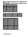
List of Tables
Table 1: Peripheral interface signals ............................................................................................... 11
Table 2: Direct connection to some peripheral interface signals..................................................... 12
Table 3: UART connector pin assignments..................................................................................... 16
Table 4: I2C connectors of the carrier board.................................................................................... 18
Table 5: Analog input connector...................................................................................................... 19
Table 6: I2C connectors of the carrier board.................................................................................... 19
Table 7: Connector pin assignments for the peripheral interface.................................................... 25
Table 8: I/O pin connector pin assignments for the carrier board and the MCM............................. 26
Table 9: UART interface connector pin assignments for the carrier board and the MCM ............... 26
Table 10: McBSP interface pin assignments for the carrier board and the MCM ........................... 26
Table 11: I2C interface pin assignments for the carrier board and the MCM................................... 27
Table 12: Analog input pin assignments for the carrier board and the MCM .................................. 27
Table 13: Reset signal pin assignments for the carrier board and the MCM .................................. 27
Table 14: Power pin assignments for the carrier board................................................................... 27
Table 15: Reset signal pin assignments for the carrier board and the MCM .................................. 27
Table 16: IEEE1394 cable power supply for the carrier board........................................................ 27
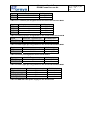
Table 17: Pinout for micro-line® connector A .................................................................................. 28
Table 18: Pinout for micro-line® connector B .................................................................................. 29
Table 19: Pinout for micro-line® connector BB ................................................................................ 30
Table 20: Pinout for micro-line® connector C .................................................................................. 31
Table 21: Pinout for micro-line® connector D .................................................................................. 32
Table 22: Pinout for micro-line® connector E .................................................................................. 33
Table 23: Pinout for micro-line® connector P .................................................................................. 34
Table 24: Pinout for micro-line® connector X .................................................................................. 34
Table 25: Pinout for the alternative RS-232 connector ................................................................... 35
Table 26: Pinout for the analog input connector.............................................................................. 35
Table 27: Pinout for the JTAG connector ........................................................................................ 35
List of Figures
Figure 1: DCAM frame capture kit block diagram ............................................................................. 7
Figure 2: UC1394a carrier board connectors and control elements.................................................. 8
Figure 3: Power supply board connectors and control elements ...................................................... 9
Figure 4: Block diagram of the peripheral interface......................................................................... 10
Figure 5: Isochronous data, recorded from the IEEE1394 bus with an analyzer ............................ 13
Figure 6: Isochronous packet assembly, sampling at 100kHz, 16bit, packet size = 40 bytes......... 14
Figure 7: IEEE1394 power supply options of the carrier board....................................................... 15
Figure 8: UART interface block diagram ......................................................................................... 16
Figure 9: I/O pin block diagram ....................................................................................................... 17
Figure 10: McBSP block diagram.................................................................................................... 18
Figure 11: JTAG Adapter ................................................................................................................ 20
Figure 12: JTAG Adapter (with FPGA JTAG signals shown) .......................................................... 20
Figure 13: Sample session of the hello example............................................................................. 22
Figure 14: Waveforms generated by the periph_if example............................................................ 24
HARDWARE USER'S GUIDE
DCAM FRAME CAPTURE KIT
Date
: 17 February 2005
Doc. no. : DCAM_FC_HG
Iss./Rev : 1.00
Page
:5
1 Preface
This document describes the hardware platform for the UC1394a-1 based DCAM frame capture
kit. It is intended to get an overview of the whole kit and the features provided by the carrier board.
Detailed information about programming, FPGA usage and UC1394a-1 technical data is contained
in other documents that will be referenced throughout this document. FPGA development is not
supported by the DCAM frame capture kit, but available as a separate product.
1.1
Document Organization
This document is organized as follows:
• Chapter 2 gives a brief overview of the whole system and its interfaces
• Chapter 3 tells how to do the very first steps
• Chapter 4 lists technical data of the kit, such as pinning
• Chapter 5 lists documents that contain further information
• Chapter 6 explains the abbreviations that are used throughout this document
1.2
Documentation Overview
This chapter lists the documentation from Orsys that is shipped together with the DCAM frame
capture kit. Further documents from other vendors may also be listed in chapter 5 and are
referenced throughout the document in square brackets.
DCAM API User's Guide for UC1394a-1 [1] (DCAM_UG.pdf):
Describes the DCAM frame capture API, thus the software programming interface of the DCAM
frame capture kit.
DSP Master BSP User's Guide [2] (DSP_Master_BSP_UG.pdf):
Describes the DSP Master Board Support Package (BSP) on which the DCAM frame capture kit is
based. This includes FPGA register description, programming documentation and technical data of
the UC1394a-1 MCM.
micro-line® Power Supply Kit [3] (Power_Supply.pdf):
Describes the micro-line® Power Supply board.
1.3
Notational conventions
Names of registers, bit fields and single bits are written in capital letters.
Example: LLC_VERSION
Names of signals are also given in capital letters, active low signals are marked with a '/' at the
beginning of the name.
Example: /RESETIN
Configuration parameters, function names, path names and file names are written in italic typeface.
Example: dev_id
Source code examples are given in a small, fixed-width typeface.
Example: int a = 10;
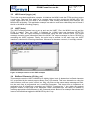
Menus and commands from menus and submenus are enclosed in double-quotes. Example:
Create a new project using the "Create Project..." command from the "File" menu.
The members of a bit field or a group of signals are numbered starting at zero, which is the least
significant bit.
Date
: 17 February 2005
Doc. no. : DCAM_FC_HG
Iss./Rev : 1.00
Page
:6
HARDWARE USER'S GUIDE
DCAM FRAME CAPTURE KIT
Example: CFG[4:0] identifies a group of five signals, where CFG0 is the least significant bit and
CFG4 is the most significant bit.
If necessary, numbers are represented with a suffix that specifies their base.
Example: 12AB16 is a hexadecimal number (base 16 = hexadecimal) and is equal to 477910.
The bit fields of a register are displayed with the most significant bit to the left. Below each bit field
is a description of its read / write accessibility and its default value:
bit number
bit name
15
14
13
12
11
10
6
5
4
3
2
1
0
A
B
C
D
E
F
9
G
8
7
H
I
J
K
L
N
O
r,w,0
r,w,0
r,w,0
r,w,0
r,w,0
r,w,0
r,w,0102
r,0
r,wc,0
w
r,w,0
rc,0
r,w,0
r,w,0
accessibility and default value
legend:
r
bit is readable
rc
this bit is cleared after a read
r,w bit is readable and writeable, reading yields the previously written value unless otherwise
specified.
w
bit is writeable, read value is undefined
wc writing a '1' to this bit clears it
w,0 bit is write-only, reading always yields 0.
0
default value
1.4
Trademarks
TI, Code Composer, DSP/BIOS and TMS320C5000 are registered trademarks
of Texas Instruments.
Microsoft® and Windows® are either registered trademarks or
trademarks of Microsoft Corporation in the United States and/or other
countries.
Hypterterminal is a trademark of Hilgraeve Inc.
All other brand or product names are trademarks or registered trademarks of
their respective companies or organizations.
1.5
Revision history
Revision
1.0
Changes
First public release.
Replaces uc1394a1_dsp_dev_kit_hrg for the DCAM frame capture kit.
HARDWARE USER'S GUIDE
DCAM FRAME CAPTURE KIT
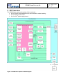
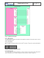
2 Kit Overview
The DCAM frame capture kit consists of three modules:
• An UC1394a-1 MCM soldered on a carrier board for easier handling
• An UC1394a carrier board
• A micro-line® power supply board
Figure 1: DCAM frame capture kit block diagram
Date
: 17 February 2005
Doc. no. : DCAM_FC_HG
Iss./Rev : 1.00
Page
:7
HARDWARE USER'S GUIDE
DCAM FRAME CAPTURE KIT
2.1
Date
: 17 February 2005
Doc. no. : DCAM_FC_HG
Iss./Rev : 1.00
Page
:8
UC1394a-1 MCM
The UC1394a-1 MCM is the heart of the DCAM frame capture kit. It provides all of the interfaces
shown in Figure 1 and a complete hardware environment for user applications. After software
development is finished, the UC1394a-1 can be easily integrated into a customized hardware
environment. Its small size and low cost make it an ideal solution for end-product usage. Further,
the implementation as a multi chip module (MCM) allows similar handling as of integrated circuits,
therefore mass production is supported.
The MCM is equipped with the DSP master board support package (BSP). This BSP provides
software driven access to IEEE1394 streaming data and a peripheral interface to connect a wide
range of peripherals. The DSP master BSP is described in [2].
2.2
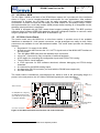
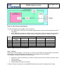
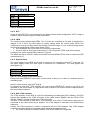
UC1394a Carrier Board
The carrier board turns the MCM into a micro-line® module. It provides most of the available
interfaces on standard 0.1 inch spaced connectors, so that prototypes can easily be built. Other
connectors are available for use with dedicated cables. The carrier board provides the following
features:
• Regulated 3.3 V supply for the MCM.
• A level converter that converts the 3.3 V LVTTL signal levels of the MCM UART interface to
RS-232 levels.
• Two 400 Mbps IEEE1394 ports with standard 6 pin connectors.
• micro-line® connector for easy connection of external hardware.
• A DIP-switch for controlling the configuration inputs and FPGA JTAG routing.
• Three LEDs for visual feedback.
• A JTAG connector for DSP software download, software debugging and FPGA design
download.1
• A connector for the MCM's analog inputs
• An alternative RS-232 connector (not used with the DCAM frame capture kit)
• An USB connector
The carrier board is intended as a development aid, which is used in the prototyping stage of a
project. In the end product, the UC1394a-1 MCM will typically be used standalone.
analog in
c onnector
A
B
BB
JTAG connector
USB
c onnector
red LED (FPGA not configured)
red LED (user programmable)
green LED (user programmable)
IEEE1394
c onnectors
c onfiguration DIP-switch
micro-line c onnectors
XP
C
D
E
Figure 2: UC1394a carrier board connectors and control elements
1
MCM FPGA development is available as a separate product.
EGND
alternative RS-232
c onnector
Date
: 17 February 2005
Doc. no. : DCAM_FC_HG
Iss./Rev : 1.00
Page
:9
HARDWARE USER'S GUIDE
DCAM FRAME CAPTURE KIT
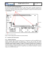
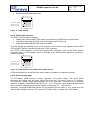
2.3
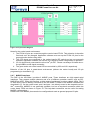
micro-line® Power Supply Board
The micro-line® power supply board acts as a desk carrier board. It provides connectors for
RS-232 and unregulated power input. Further it provides a button for resetting the MCM and the
carrier board. The power supply board generates a regulated 5 V supply for the carrier board from
an unregulated 12 V input.
micro-line connectors
power indicator LED
A
reset button
D
P
EGND
RS-232
c onnector
power input from external AC-adapter
Figure 3: Power supply board connectors and control elements
2.4
Interfaces and Connectors
2.4.1 Software Streaming
Software streaming allows to transfer large amount of data between the DSP and IEEE1394 with
minimal overhead. Data transfers are buffered by a FIFO, so that the DSP can operate
independent of the IEEE1394 timing. Streaming transfers are unidirectional and must be set up for
a particular direction before operation is started. The maximum transfer rate for streaming is
32,768,000 byte/s. Software streaming is used for receiving image data from the connected
cameras. Isochronous streaming is explained in chapter 2.4.3. Programming is described in [1] and
in [2]. The distribution media contains an example that uses software streaming for capturing
images from an IEEE1394 camera.
HARDWARE USER'S GUIDE
DCAM FRAME CAPTURE KIT
Date
: 17 February 2005
Doc. no. : DCAM_FC_HG
Iss./Rev : 1.00
Page
: 10
2.4.2 micro-line® Peripheral Interface
The micro-line® peripheral interface allows to connect micro-line® peripheral boards, as well as a
wide range of user-defined peripherals. The micro-line® peripheral interface is implemented as a
parallel bus interface with asynchronous control signals. All signals of the peripheral interface of
the MCM are routed to the micro-line® connectors through the carrier board FPGA. Additionally,
some signals are directly routed to the C and E connectors. However, user-defined hardware
should only use the default micro-line® signals (routed through the FPGA) in order to be compatible
with other micro-line® CPU boards. Further, the directly connected data lines on the C-connector
are used at system startup for booting the carrier board FPGA.
Figure 4: Block diagram of the peripheral interface
A detailed functional description of the peripheral interface can be found in [1]. The standard microline® signals are listed in Table 1, whereas the directly connected signals are listed in Table 2.
HARDWARE USER'S GUIDE
DCAM FRAME CAPTURE KIT
Signal
ADDR0
ADDR1
ADDR2
ADDR3
ADDR4
ADDR5
ADDR6
ADDR7
DATA0
DATA1
DATA2
DATA3
DATA4
DATA5
DATA6
DATA7
DATA8
DATA9
DATA10
DATA11
DATA12
DATA13
DATA14
DATA15
/CS1
/CS2
/CS3
/CS4
/CS5
/CS6
/CS7
/IORD
/IOWR
IOR/W
/IOSTRB
IORDY
/INT3
/INT4
ML Connector pin
B1
B1
B3
B4
B5
B6
B7
B8
A1
A2
A3
A4
A5
A6
A7
A8
A9
A10
A11
A12
A13
A14
A15
A16
D10
D11
D12
D13
D14
D15
D16
D22
D23
D24
D25
D30
D17
D18
Table 1: Peripheral interface signals
Signal group
address lines
data lines
chip select lines
control signals
interrupts
Date
: 17 February 2005
Doc. no. : DCAM_FC_HG
Iss./Rev : 1.00
Page
: 11
HARDWARE USER'S GUIDE
DCAM FRAME CAPTURE KIT
Signal
DATA0
DATA1
DATA2
DATA3
DATA4
DATA5
DATA6
DATA7
DATA8
DATA9
DATA10
DATA11
DATA12
DATA13
DATA14
DATA15
/IORD
/IOWR
IOR/W
/IOSTRB
IORDY
ML Connector pin
C1
C2
C3
C4
C5
C6
C7
C8
C9
C10
C11
C12
C13
C14
C15
C16
E5
E6
E1
E3
E2
Date
: 17 February 2005
Doc. no. : DCAM_FC_HG
Iss./Rev : 1.00
Page
: 12
Signal group
data lines
control signals
Table 2: Direct connection to some peripheral interface signals
2.4.3 IEEE1394 Interface
The UC1394a-1 MCM has two 400 Mbps IEEE1394 ports. These ports are routed to two standard
6-pin IEEE1394 connectors on the carrier board. Using these two ports, the DCAM frame capture
kit can be inserted anywhere in an existing IEEE1394 network. Since the IEEE1394 physical layer
acts as a repeater, no processing power is required for transferring data from one port to the other.
For transferring data between the DCAM frame capture kit and the IEEE1394 network, three
transfer methods are available which are described in the following chapter.
2.4.4 IEEE1394 Data Transfer Methods
IEEE1394 provides three different methods for transferring data:
• isochronous streaming
• asynchronous streaming
• asynchronous transactions
Asynchronous transactions are handled by the IEEE1394 API, whereas isochronous and
asynchronous streaming is only set up by the API and then performed by FPGA register accesses.
2.4.4.1 Isochronous Streaming
In isochronous streaming, data is transferred in regular intervals, called cycles. In each cycle, one
data packet can be transferred. The size of these data packets determines the maximum data
bandwidth which can be calculated as max_bandwidth = packet_size * 8000 packets_per_second.
The cycle clock is 8kHz, therefore, packets get sent every 125 µs. Before transmission is started,
the transmitter reserves the necessary amount of bus bandwidth at a central location on the bus,
the isochronous resource manager. This and the fact that isochronous packets have precedence
over asynchronous packets guarantees, that the bus provides enough capacity for the transfer.
Isochronous streaming is an excellent solution for transferring image data from a camera.
Isochronous transfers are multicast transfers which are identified by a channel, so there is always
HARDWARE USER'S GUIDE
DCAM FRAME CAPTURE KIT
Date
: 17 February 2005
Doc. no. : DCAM_FC_HG
Iss./Rev : 1.00
Page
: 13
one talker but there may be one or more listeners. The transfer is typically done without any
software overhead and is therefore quite fast. Error detection is done at the receiver side.
Isochronous streaming is well suited for
• large amounts of data
• data distribution to several devices
• data that occurs in regular intervals
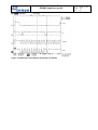
Figure 5 shows a part of an isochronous stream, recorded with an analyzer. The large blocks are
isochronous packets with maximum size (4096 bytes). The isochronous packets are preceded by a
cycle start packet, which indicates the start of a new cycle. On the UC1394a-1 MCM, packets are
only transmitted, when enough data is present in the FIFO. Otherwise, the corresponding cycle will
be empty, thus, no packet is transmitted. Figure 6 shows an example for this.
Figure 5: Isochronous data, recorded from the IEEE1394 bus with an analyzer
HARDWARE USER'S GUIDE
DCAM FRAME CAPTURE KIT
Date
: 17 February 2005
Doc. no. : DCAM_FC_HG
Iss./Rev : 1.00
Page
: 14
Figure 6: Isochronous packet assembly, sampling at 100kHz, 16bit, packet size = 40 bytes2
2.4.4.2 Asynchronous Streaming
Asynchronous streaming is similar to isochronous streaming. Asynchronous streaming uses the
same data packets as an isochronous transfer. Packets may be sent anytime, provided that the
bus is free. Bus bandwidth is not guaranteed here, so the transmission of a packet may be blocked
by other transfers on the bus. At the receiver side it makes no difference whether isochronous or
asynchronous streaming is used. Asynchronous streaming should be used, when latency
requirements don't allow isochronous streaming and bus bandwidth can be guaranteed by system
design.
2.4.4.3 Asynchronous Transactions
Asynchronous transactions are handled by the DCAM API for control of the connected cameras.
Each data packet that is sent, receives a response from the addressed device. Asynchronous
transfers can occur at any time (provided that the bus is free). They are point to point transfers, so
the originator of the transfer must know who to talk to. An asynchronous transfer consists of a
request that is sent to the destination device, and a response that the destination device sends
back. This enables error checking at the sender. Asynchronous transfers are well suited for
• data that occurs randomly (e.g. control and status information)
• transfers where the originator of the transfer must be informed about the status of each
single transfer
2.4.4.4 Plug & Play features of IEEE1394
When devices are connected to or disconnected from the IEEE1394 network, node ID's are
automatically assigned for the connected devices. This is done by the chipset without any software
intervention. Independent of the node ID, most devices provide some more information about
themselves. There is an area within the IEEE1394 address space that is called configuration ROM.
The configuration ROM holds information about
• the manufacturer of the device
• device serial number
• software interface of the device
The serial number together with the manufacturer form a world wide unique 64 bit ID. Using this 64
bit ID, the device can be identified independently of the network topology or the currently assigned
node ID.
The next higher level of identification is the protocol level. The DCAM frame capture kit identifies
itself as a device running a generic protocol specified by Orsys. This protocol can be used on a
host PC to load appropriate device drivers. Customized protocol identification is available from
Orsys on request.
2
This picture shows isochronous transmit operation, which is not used in the DCAM fame capture kit.
HARDWARE USER'S GUIDE
DCAM FRAME CAPTURE KIT
Date
: 17 February 2005
Doc. no. : DCAM_FC_HG
Iss./Rev : 1.00
Page
: 15
2.4.4.5 Power Distribution Over IEEE1394
The IEEE1394 standard defines a 6-wire cable, that allows to supply devices over the cable. This
is often used for digital cameras. To operate the UC1394a-1 powered from the IEEE1394 cable, an
external voltage regulator is required. The IEEE1394 standard allows up to 10W power
consumption for a device. Figure 7 shows the power supply options that are available for the
carrier board in standard configuration.
Figure 7: IEEE1394 power supply options of the carrier board
2.4.4.6 Isolation
The IEEE1394 interface of the UC1394a-1 is directly connected to the remaining circuit. There is
no galvanic isolation between the IEEE1394 cable and the local power supply. In a custom
hardware design, the VG pin of the 1394 connector must be connected to the GND pins of the
UC1394a-1.
2.4.5 UART Interface
The UC1394a-1 MCM has an UART interface that can be used for standard asynchronous
communication. Different baud rates are supported as well as RTS/CTS handshake. The carrier
board uses a level converter to convert these signals to RS-232 level. How to program the UART
interface is described in [1]. The distribution media contains an application example for the UART
in the hello folder. The UART interface uses 2 data lines and 2 handshake lines. A detailed
description of the UART signals can be found in [1].
HARDWARE USER'S GUIDE
DCAM FRAME CAPTURE KIT
Date
: 17 February 2005
Doc. no. : DCAM_FC_HG
Iss./Rev : 1.00
Page
: 16
Figure 8: UART interface block diagram
The RS-232 signals are available at two connectors:
• on a 9-pin sub-D connector on the power supply board, routed via the standard micro-line®
connectors
• on an alternative connector, located on the carrier board. This connector can be used for
direct cable connections to the carrier board. A suitable receptacle is listed in chapter 4.5.
Signal
TxD
RxD
RTS
CTS
GND
carrier board
10-pin
5
3
4
8
9, 10
Connector
micro-line®
Sub-D 9-pin
D26
D28
D27
D29
D1 .. D4
3
2
7
8
5
Cable connection to a remote PC
Sub-D 9-pin
Sub-D 25-pin
2
3
8
7
5
3
2
5
4
7
Table 3: UART connector pin assignments
2.4.6 I/O Pins
Please note: With exception of the XF pin, all I/O pins of the MCM are implemented in the FPGA,
whereas the (on-chip) GPIO pins of the DSP are not available on the UC1394a-1.
The available I/O pins are divided into three groups:
•
•
•
FPGA I/O: a part of these pins is used as outputs by the carrier board, the other part is
used as inputs.
configuration inputs
external flag (XF) output of the DSP
If further I/O pins are required, unused McBSP interfaces can also be configured as I/O pins.
HARDWARE USER'S GUIDE
DCAM FRAME CAPTURE KIT
Date
: 17 February 2005
Doc. no. : DCAM_FC_HG
Iss./Rev : 1.00
Page
: 17
Figure 9: I/O pin block diagram
Notes for the carrier board environment:
1. The FPGA I/O pins are routed through the carrier board FPGA. Their direction is therefore
fixed and can't be changed. Application software must set up the FPGA I/O pins for the
proper direction before using them.
2. The CFG inputs are connected to the carrier board's DIP switch and are not externally
available. Application software can use the CFG inputs for basic configuration of operation.
3. I/O 4 is also directly connected the micro-line® pin E27. Please use always I/O4 with micro–
line pin BB5 to avoid signal contention.
4. The green and a red carrier board LED are controlled by I/O0 and I/O1 respectively.
Behavior of the I/O pins in stand-alone environment (without the carrier board) and I/O pin
programming is described in [1].
2.4.7 McBSP Interfaces
The DSP of the UC1394a-1 provides 3 McBSP ports. These interfaces are high speed serial
interfaces. They support multiple channels and a lot of different operation modes, such as SPI,
MMC/SD or AC97. Using this interface, a wide range of peripherals, such as codecs, ADCs, DACs
or other DSP's can be directly connected to the UC1394a-1. Details of the McBSP interfaces are
described in [1]. On the carrier board, port 0 and port 1 are directly routed to the respective microline® connectors. McBSP2 is not externally available, but has a loop-back connection within the
carrier board FPGA as shown in Figure 10. This loop-back connection can be useful for testing
McBSP configurations.
Please note: The McBSP pins can also be configured and used as general purpose I/O pins.
HARDWARE USER'S GUIDE
DCAM FRAME CAPTURE KIT
Date
: 17 February 2005
Doc. no. : DCAM_FC_HG
Iss./Rev : 1.00
Page
: 18
Figure 10: McBSP block diagram
2.4.8 USB Interface
The USB interface is directly connected to the respective connector of the carrier board. It can be
used as described in [1].
2.4.9 I2C Interface
The I2C signals are directly routed to the micro-line® connector. They can be used as described in
[1].
Signal
SCL
SDA
ML Connector pin
X5
X4
Table 4: I2C connectors of the carrier board
2.4.10 Analog Inputs
The analog inputs are directly connected to a 10-pin connector on the carrier board. They can be
used as described in [1]. A suitable receptacle for this connector is listed in chapter 4.5.
HARDWARE USER'S GUIDE
DCAM FRAME CAPTURE KIT
Signal
AIN0
AIN1
AIN2
AIN3
GND
Date
: 17 February 2005
Doc. no. : DCAM_FC_HG
Iss./Rev : 1.00
Page
: 19
Connector pin
1
3
5
7
2, 4, 6, 8, 9, 10
Table 5: Analog input connector
2.4.11 RTC
Usage of the DSP RTC is not supported by the default carrier board configuration. If RTC usage is
required, please contact Orsys for further information.
2.4.12 LEDs
The carrier board provides three LEDs. Two of them are controlled by I/O pins as described in
chapter 2.4.6. A third, red LED lights at system startup while the carrier board FPGA isn't
configured. It must go off after about one second. If this LED stays on, one of the following reason
may prevent configuration of the carrier board FPGA:
• the PROM with the FPGA code is not correctly programmed
• A bus conflict on micro-line® connectors C1..C8 corrupts the FPGA code during startup
Location of the carrier board LEDs is shown in Figure 2.
The MCM also has a red LED, which is controlled over the MCM's FPGA. How to access this LED
is described in [1].
2.4.13 System Reset
The reset signals of the MCM are directly connected to the respective micro-line® connector. On
the power supply board, the reset input is connected to a pushbutton. The reset signals are
described in [1].
Signal
/RESETIN
/RESETOUT
ML Connector pin
D7
D8
Table 6: I2C connectors of the carrier board
Please note that /RESETIN is driven for a short period of about 1µs in case of a software reset or
watchdog reset.
Note for users of other micro-line® boards:
In contrast to micro-line® CPU modules, the non-inverted RESETOUT signal on pin D9 is not
available on the carrier board. If a high-active reset is required, an inverter must be implemented in
the surrounding hardware.
2.4.14 DSP JTAG interface
The JTAG interface of the DSP is used for downloading and debugging DSP software. All JTAG
signals are available at the JTAG connector of the carrier board, together with the FPGA JTAG
signals. Table 27 lists the pinning of the JTAG connector.
The DSP JTAG interface is used with a JTAG emulator, such as the TI XDS series, which can be
connected to the carrier board by an adapter. The JTAG adapter is included in the DCAM frame
capture kit.
Usually, the JTAG connector is used in conjunction with the JTAG adapter. This JTAG adapter
provides connectors which are compatible with standard development tools:
• the Texas Instruments emulator cables, such as the XDS510 or compatible
HARDWARE USER'S GUIDE
DCAM FRAME CAPTURE KIT
•
Date
: 17 February 2005
Doc. no. : DCAM_FC_HG
Iss./Rev : 1.00
Page
: 20
the Xilinx parallel download cable
A13
A1
B13
B1
FPGA JTAG c onnec tor
DSP JTAG c onnec tor
(fits TI emulator POD)
top view
Figure 11: JTAG Adapter
2.4.15 FPGA JTAG interface
The FPGA JTAG interface is used for
• updating the carrier board FPGA code by programming a PROM on the carrier board,
• temporarily downloading FPGA code to the carrier board FPGA and
• temporarily downloading FPGA code to the MCM
All JTAG signals are available at the JTAG connector of the carrier board, together with the DSP
JTAG signals. Table 27 lists the pinning of the JTAG connector.
The FPGA JTAG interface is used with programming hardware, such as the Xilinx parallel
download cable. A JTAG adapter, which is included in the DCAM frame capture kit, provides a
suitable connector.
A13
A1
B13
B1
+3.3V GND TCK TDO TDI TMS
FPGA JTAG c onnec tor
DSP JTAG c onnec tor
(fits TI emulator POD)
top view
Figure 12: JTAG Adapter (with FPGA JTAG signals shown)
FPGA development for the MCM or the carrier board is available as a separate product.
2.4.16 Power Supply Input
The UC1394a-1 MCM requires a single, regulated 3.3 V power supply. The carrier board
generates this voltage from the power input of the micro-line® connectors, which is 5 V nominal.
The micro-line® power supply board supplies 5V to the micro-line® connector from a switching
regulator. It allows unregulated power input of 9 V .. 12 V. The power supply board can be supplied
from a usual AC adapter, which must be capable of delivering 9 V .. 18 V and 4W.
Optionally, connected IEEE1394 devices can be supplied over the cable. In turn, power from the
cable is also available at micro-line® connector P. Please refer to chapter 2.4.4.5 for details.
HARDWARE USER'S GUIDE
DCAM FRAME CAPTURE KIT
Date
: 17 February 2005
Doc. no. : DCAM_FC_HG
Iss./Rev : 1.00
Page
: 21
3 Application Examples
The distribution media contains two kinds of application examples:
• DCAM-specific examples
• Examples from the DSP master BSP
How to use the DCAM-specific examples is described in [1], whereas the BSP examples are
described in the subsequent sections. The examples can either be downloaded to the kit by using
a JTAG emulator or they can be programmed to the MCM's flash memory as described in [1]. To
download an application example to the MCM, please proceed as follows:
Required items:
•
•
•
•
•
a development PC, with the software listed below installed.
Texas Instruments Code Composer Studio (CCS) V2.2x. A run time limited version is
downloadable from www.ti.com.
a JTAG emulator
a terminal program, such as Hyperterminal, which is usually part of Windows distributions
a DCAM frame capture kit, including a JTAG adapter, all cables and a suitable power
supply
All application examples are provided as a CCS project. The project has two available
configurations: Debug and Release. Debug is the default configuration and should be used during
development. The Release configuration differs from Debug in two points:
•
•
no debugging symbols are created, the code is not suitable for source code debugging, but
better optimized
The Release version of the module support library is used
The Release configuration should be used for the final application after development is finished.
Further, all example projects contain a final build step that creates a .hex file. This file can be
programmed to flash memory as described in [1].
3.1
Download procedure
•
•
•
•
•
•
•
•
•
connect the kit to the development PC using the JTAG emulator / JTAG adapter and the
RS-2332 cable
power on the system
start Code Composer Studio
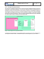
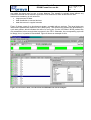
select the "Load GEL..." command from the "File" menu
locate uc1394a-1_master.gel from the GEL folder on the distribution media and open it
select the "Initialization"->"CPU_reset_and_init_144Mhz" command from the "GEL" menu
select the "Load Program..." command from the "File" menu
locate one of the application examples from the examples folder on the distribution media
and open it (e.g. toggle_led.out)
select the "Run" command from the "Debug" menu
Please note: the application examples do not use the usual printf function. Instead, where
necessary, output is sent over the UART interface (using 115200 baud and RTS/CTS handshake).
This allows to store the examples in flash memory and then to execute them without the JTAG
emulator.
HARDWARE USER'S GUIDE
DCAM FRAME CAPTURE KIT
Date
: 17 February 2005
Doc. no. : DCAM_FC_HG
Iss./Rev : 1.00
Page
: 22
3.2
LED Control (toggle_led)
This is the most basic application example. It initializes the MCM, loads the FPGA and then enters
a main loop. The main loop waits for a constant delay and then toggles the MCM's LED. The
carrier board LEDs are not used in this example. After loading and starting this example. the
MCM's LED is blinking. This application example can also be used as a rudimentary test to check if
the kit or the MCM is working properly.
3.3
UART (hello)
The UART example shows how to set up and use the UART. First, the MCM is set up and the
FPGA is loaded. Then, the UART is initialized for 115200 baud and hardware (RTS/CTS)
handshake. Then, an output message is assembled using the stdio function sprintf. The output
message contains some information about the MCM. The output message is sent to RS-232 by
accessing the UART registers. Finally, the main loop is entered. In the main loop, the UART
interface is checked for incoming characters. Whenever a character comes in, it is simply echoed.
Figure 13: Sample session of the hello example
3.4
Buffered Character I/O (dbg_out)
This example uses the UART interface at a slightly higher level of abstraction: buffered character
I/O, as provided by the module support library, see [1] for details. This is an alternative to using the
stdio functions, such as sprintf, sscanf, etc. dbg_out prints out the same startup message as hello,
but the main loop is programmed as a command interpreter. This shows how to implement an
application that is interactively controlled over RS-232. Pressing the '?' key within the terminal
program causes a help page to be displayed. Other command keys can easily be added by
inserting appropriate case statement in the command switch. Below is an example that shows how
insert a command that toggles the MCM LED by the 't' key:
HARDWARE USER'S GUIDE
DCAM FRAME CAPTURE KIT
Date
: 17 February 2005
Doc. no. : DCAM_FC_HG
Iss./Rev : 1.00
Page
: 23
//below is a command switch that could be used in applications
//that require user interaction over RS_232
switch(c)
{
case '?':
case 'h':
DebugOutConstString("Debug interface example\r\n");
DebugOutConstString("'h' and '?' show this help page\r\n"
"no other commands/keys defined\r\n");
break;
case 't':
//toggle the red MCM LED
UC1394A_SYS_CTL^= UC1394A_SYS_LED;
break;
default:
DebugOutConstString("invalid command. "
"'?' shows a help page.\r\n");
break;
}
}
3.5
I/O Pins (io_pin)
The io_pin example works together with the carrier board LEDs. It doesn't generate any output,
except for the visual feedback through the carrier board LEDs. After the usual startup, I/O0 and
I/O1 are configured as outputs and I/O3 is configured as an input, according to the direction
predefined by the carrier board (see also Figure 9). In the main loop, the red LED of the carrier
board is continuously toggled so that it is blinking. The green LED is controlled by the state of I/O
3. For testing, I/O3 (micro-line® connector pin BB4) can be connected to one of the following
connector pins by a 1kΩ series resistor:
a) (none):
The green LED is lighting, caused by IO3's built-in pull-up
resistor.
b) GND (pin D1):
The green LED is switched off
b) I/O1 (controls the red LED; pin BB2): The green LED is also blinking
3.6
Peripheral Interface (periph_if)
This application example has neither any text output, nor does it control the LEDs. It is mainly
intended as a source code example. Further, the peripheral interface signals can be viewed with
an oscilloscope or a logic analyzer. After the usual initialization, the main loop performs the
following sequence:
• pulse XFOUT as a trigger signal
• write an all-zeros pattern to the first address of /CS1
• write an all-ones pattern to the last address of /CS1
• repeat the last 2 steps for /CS2 through /CS7
• do a dummy read from the first address of /CS1
• repeat the last step for /CS2 through /CS7
• repeat the complete sequence
Figure 14 shows some waveforms that were generated by this example. The left cursor shows the
start of the sequence. The right cursor shows a common programming issue for the DSP EMIF,
which is also described in [1], chapter "Pipeline": The last write operation (/CS7, highest address,
pattern 0xFFFF) is immediately followed by a read operation (/CS1). Since the write operation
needs some pipeline steps to prepare the peripheral access, the read operation appears before
the write operation. Such situations must be avoided as described in [1].
HARDWARE USER'S GUIDE
DCAM FRAME CAPTURE KIT
Figure 14: Waveforms generated by the periph_if example
Date
: 17 February 2005
Doc. no. : DCAM_FC_HG
Iss./Rev : 1.00
Page
: 24
HARDWARE USER'S GUIDE
DCAM FRAME CAPTURE KIT
Date
: 17 February 2005
Doc. no. : DCAM_FC_HG
Iss./Rev : 1.00
Page
: 25
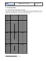
4 Technical Data
4.1
Connector Pinout Summary by Interface
The tables in this chapter list the connector pin assignments for each interface separately. The pin
assignments show both pinouts, for the carrier board and the UC1394a-1 MCM. This allows easy
migration from the DCAM frame capture kit to a standalone system.
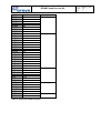
Signal
ADDR0
ADDR1
ADDR2
ADDR3
ADDR4
ADDR5
ADDR6
ADDR7
DATA0
DATA1
DATA2
DATA3
DATA4
DATA5
DATA6
DATA7
DATA8
DATA9
DATA10
DATA11
DATA12
DATA13
DATA14
DATA15
/CS1
/CS2
/CS3
/CS4
/CS5
/CS6
/CS7
/IORD
/IOWR
IOR/W
/IOSTRB
IORDY
/INT3
/INT4
ML Connector pin
B1
B1
B3
B4
B5
B6
B7
B8
A1
(C13)
A2
(C2)
A3
(C3)
A4
(C4)
A5
(C5)
A6
(C6)
A7
(C7)
A8
(C8)
A9
(C9)
A10
(C10)
A11
(C11)
A12
(C12)
A13
(C13)
A14
(C14)
A15
(C15)
A16
(C16)
D10
D11
D12
D13
D14
D15
D16
D22
(E5)
D23
(E6)
D24
(E1)
D25
(E3)
D30
(E2)
D17
D18
MCM connector pin
D6
D7
D8
D9
D10
D11
D12
D13
B3
B4
B5
B6
B7
B8
B9
B10
B12
B13
B14
B15
B16
B17
B18
B19
D14
D15
D16
D17
D23
D24
D25
B22
B21
B24
B23
B25
D26
D27
Table 7: Connector pin assignments for the peripheral interface
3
Directly connected to the MCM. Do not use.
HARDWARE USER'S GUIDE
DCAM FRAME CAPTURE KIT
Signal
I/O0
I/O1
I/O2
I/O3
I/O4
XFOUT
CFG0
CFG1
CFG2
CFG3
CFG4
micro-line® connector pin
BB1
BB2
BB3
BB4
BB5
(E27)
E26
n/a
n/a
n/a
n/a
n/a
Date
: 17 February 2005
Doc. no. : DCAM_FC_HG
Iss./Rev : 1.00
Page
: 26
UC1394a-1 pin
D19
D20
D21
D22
C27
C26
A12
A13
A14
A15
A16
Table 8: I/O pin connector pin assignments for the carrier board and the MCM
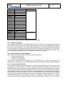
Signal
TxD
RxD
RTS
CTS
micro-line® connector pin
D26
D28
D27
D29
Alternative connector
5
3
4
6
UC1394a-1 pin
(A174)
(A18)
(A19)
(A20)
Table 9: UART interface connector pin assignments for the carrier board and the MCM
Signal
DR0
DX0
CLKR0
CLKX0
FSR0
FSX0
DR1
DX1
CLKR1
CLKX1
FSR1
FSX1
DR2
DX2
CLKR2
CLKX2
FSR2
FSX2
micro-line® connector pin
E20
E21
E22
E23
E24
E25
E10
E11
E12
E13
E14
E15
n/a
n/a
n/a
n/a
n/a
n/a
UC1394a-1 pin
A3
A4
A5
A6
A7
A8
C1
C2
C3
C4
C5
C6
C8
C9
C10
C11
C12
C13
Table 10: McBSP interface pin assignments for the carrier board and the MCM
4
3.3V signal level! Level converter required!
HARDWARE USER'S GUIDE
DCAM FRAME CAPTURE KIT
Signal
SCL
SDA
micro-line® connector pin
X5
X4
UC1394a-1 pin
D32
D31
Table 11: I2C interface pin assignments for the carrier board and the MCM
Signal
AIN0
AIN1
AIN2
AIN3
Analog input connector pin
1
3
5
7
UC1394a-1 pin
C29
C30
C31
C32
Table 12: Analog input pin assignments for the carrier board and the MCM
Signal
/RESETIN
/RESETOUT
micro-line® connector pin
D7
D8
UC1394a-1 pin
A10
A9
Table 13: Reset signal pin assignments for the carrier board and the MCM
Signal
D+5V
GND
micro-line® connector pin
D5, D6
D1..D4
UC1394a-1 pin
n/a, see [1]
see [1]
Table 14: Power pin assignments for the carrier board
Signal
/RESETIN
/RESETOUT
micro-line® connector pin
D7
D8
UC1394a-1 pin
A10
A9
Table 15: Reset signal pin assignments for the carrier board and the MCM
Signal
+8 V.. + 30 V
GND
CABLE_POWER
CABLE_GND
micro-line® connector pin
P6
P7
P10
P9
UC1394a-1 pin
n/a
n/a
n/a
n/a
Table 16: IEEE1394 cable power supply for the carrier board
Date
: 17 February 2005
Doc. no. : DCAM_FC_HG
Iss./Rev : 1.00
Page
: 27
HARDWARE USER'S GUIDE
DCAM FRAME CAPTURE KIT
4.2
Date
: 17 February 2005
Doc. no. : DCAM_FC_HG
Iss./Rev : 1.00
Page
: 28
Connector Pinout Summary by Connector
The tables in this chapter list the connector pinout for
• each micro-line® connector row
• the analog input connector
• the alternative RS-232 connector
separately.
4.2.1 Connector A
Connector A is used with the peripheral interface. It carries the micro-line® data bus.
micro-line®
connector pin
A1
A2
A3
A4
A5
A6
A7
A8
A9
A10
A11
A12
A13
A14
A15
A16
A17
A18
A19
A20
A21
A22
A23
A24
A25
A26
A27
A28
A29
A30
A31
A32
Signal
Interface
ML_D0
ML_D1
ML_D2
ML_D3
ML_D4
ML_D5
ML_D6
ML_D7
ML_D8
ML_D9
ML_D10
ML_D11
ML_D12
ML_D13
ML_D14
ML_D15
peripheral
interface
reserved
n/a
Table 17: Pinout for micro-line® connector A
HARDWARE USER'S GUIDE
DCAM FRAME CAPTURE KIT
Date
: 17 February 2005
Doc. no. : DCAM_FC_HG
Iss./Rev : 1.00
Page
: 29
4.2.2 Connector B
Connector B carries the address lines of the peripheral interface and the signal ground.
micro-line®
connector pin
B1
B2
B3
B4
B5
B6
B7
B8
B9
B10
B11
B12
B13
B14
B15
B16
B17
B18
B19
B20
B21
B22
B23
B24
B25
B26
B27
B28
B29
B30
B31
B32
Signal
Interface
ADDR0
ADDR1
ADDR2
ADDR3
ADDR4
ADDR5
ADDR6
ADDR7
peripheral interface
reserved
n/a
SIGNAL_GND
SIGNAL_GND
SIGNAL_GND
SIGNAL_GND
SIGNAL_GND
SIGNAL_GND
SIGNAL_GND
SIGNAL_GND
power supply
Table 18: Pinout for micro-line® connector B
HARDWARE USER'S GUIDE
DCAM FRAME CAPTURE KIT
4.2.3 Connector BB
Connector BB is used for the FPGA I/O pins.
micro-line®
connector pin
BB1
BB2
BB3
BB4
BB5
BB6
BB7
BB8
BB9
BB10
BB11
BB12
BB13
BB14
BB15
BB16
BB17
BB18
BB19
BB20
BB21
BB22
BB23
BB24
BB25
BB26
BB27
BB28
BB29
BB30
BB31
BB32
Signal
Interface
I/O0
I/O2
I/O3
I/O4
I/O4
I/O pins
reserved
n/a
Table 19: Pinout for micro-line® connector BB
Date
: 17 February 2005
Doc. no. : DCAM_FC_HG
Iss./Rev : 1.00
Page
: 30
HARDWARE USER'S GUIDE
DCAM FRAME CAPTURE KIT
Date
: 17 February 2005
Doc. no. : DCAM_FC_HG
Iss./Rev : 1.00
Page
: 31
4.2.4 Connector C
Connector C carries the directly connected data lines of the peripheral interface. It is strongly
recommended to leave this connector unconnected an to prefer the data lines on the A-connector.
micro-line®
connector pin
C1
C2
C3
C4
C5
C6
C7
C8
C9
C10
C11
C12
C13
C14
C15
C16
C17
C18
C19
C20
C21
C22
C23
C24
C25
C26
C27
C28
C29
C30
C31
C32
Signal
Interface
(DATA0)
(DATA1)
(DATA2)
(DATA3)
(DATA4)
(DATA5)
(DATA6)
(DATA7)
(DATA8)
(DATA9)
(DATA10)
(DATA11)
(DATA12)
(DATA13)
(DATA14)
(DATA15)
(peripheral
interface5)
reserved
n/a
Table 20: Pinout for micro-line® connector C
5
These signals should not be used on this connector. Instead, the signals on the A connector should be
used.
HARDWARE USER'S GUIDE
DCAM FRAME CAPTURE KIT
4.2.5 Connector D
Connector D is used for
• RS-232 (UART interface converted to RS-232 levels)
• power supply
• reset signals
• control and interrupt lines of the peripheral interface
micro-line®
connector pin
D1
D2
D3
D4
D5
D6
D7
D8
D9
D10
D11
D12
D13
D14
D15
D16
D17
D18
D19
D20
D21
D22
D23
D24
D25
D26
D27
D28
D29
D30
D31
D32
Signal
GND
GND
GND
GND
+5V
+5V
/RESETIN
/RESETOUT
reserved
/CS1
/CS2
/CS3
/CS4
/CS5
/CS6
/CS7
/INT3
/INT4
reserved
/IORD
/IOWR
IOR/W
/IOSTRB
TxD
RTS
RxD
CTS
IORDY
reserved
Interface
power supply
system reset
n/a
peripheral interface
n/a
peripheral interface
RS-232
peripheral interface
n/a
Table 21: Pinout for micro-line® connector D
Date
: 17 February 2005
Doc. no. : DCAM_FC_HG
Iss./Rev : 1.00
Page
: 32
HARDWARE USER'S GUIDE
DCAM FRAME CAPTURE KIT
Date
: 17 February 2005
Doc. no. : DCAM_FC_HG
Iss./Rev : 1.00
Page
: 33
4.2.6 Connector E
Connector E is used for the McBSP signals of port 0 and 1 and for some directly connected control
signals of the peripheral interface. It is strongly recommended to use leave these control signals
unconnected and to use the corresponding signals on the D-connector instead.
micro-line®
connector pin
E1
E2
E3
E4
E5
E6
E7
E8
E9
E10
E11
E12
E13
E14
E15
E16
E17
E18
E19
E20
E21
E22
E23
E24
E25
E26
E27
E28
E29
E30
E31
E32
Signal
(IOR/W)
(IORDY)
(/IOSTRB)
reserved
(/IORD)
(/IORW)
Interface
(peripheral
interface6)
n/a
(peripheral
interface)
reserved
n/a
DR1
DX1
CLKR1
CLKX1
FSR1
FSX1
McBSP1
reserved
n/a
DR0
DX0
CLKR0
CLKX0
FSR0
FSX0
XFOUT
(I/O4)
reserved
McBSP0
I/O pins7
n/a
Table 22: Pinout for micro-line® connector E
6
These signals should not be used on this connector. Instead, the signals on the A connector should be
used.
7
I/O 4 should not be used on this connector. Instead, the signals on the A connector should be used.
HARDWARE USER'S GUIDE
DCAM FRAME CAPTURE KIT
4.2.7 Connector P
Connector P can be used for supplying power to the IEEE1394 cable.
micro-line®
connector pin
P1
P2
P3
P4
P5
P6
P7
P8
P9
P10
Signal
Interface
reserved
+8 V.. + 30 V
GND
reserved
CABLE_GND
CABLE_POWER
n/a
IEEE1394 interface
n/a
IEEE1394 interface
Table 23: Pinout for micro-line® connector P
4.2.8 Connector X
Connector X carries the I2C signals.
micro-line®
connector pin
X1
X2
X3
X4
X5
X6
X7
X8
X9
X10
Signal
Interface
reserved
SDA
SCL
reserved
Table 24: Pinout for micro-line® connector X
n/a
I2C interface
n/a
Date
: 17 February 2005
Doc. no. : DCAM_FC_HG
Iss./Rev : 1.00
Page
: 34
HARDWARE USER'S GUIDE
DCAM FRAME CAPTURE KIT
4.2.9
Other Connectors
Connector pin
1
2
3
4
5
6
7
8
9
10
Signal
Interface
reserved
n/a
RxD
RTS
TxD
CTS
UART interface
reserved
n/a
GND
GND
(UART interface)
Table 25: Pinout for the alternative RS-232 connector
Connector pin
1
2
3
4
5
6
7
8
9
10
Signal
AIN0
GND
AIN1
GND
AIN2
GND
AIN3
GND
GND
GND
Interface
analog inputs
Table 26: Pinout for the analog input connector
4.2.10 JTAG Connector
Pin
A1
A2
A3
A4
A5
A6
A7
A8
A9
A10
A11
A12
A13
Signal
FPGA_TMS
FPGA_TDI
FPGA_TDO
FPGA_TCK
+3.3 V
not connected
CPU_EMU0
CPU_TCK_RET
CPU_TCK
CPU_TDO
+3.3 V
CPU_TDI
CPU_TMS
Pin
B1
B2
B3
B4
B5
B6
B7
B8
B9
B10
B11
B12
B13
Signal
GND
GND
GND
GND
GND
not connected
CPU_EMU1
GND
GND
GND
not connected
GND
/CPU_TRST
Table 27: Pinout for the JTAG connector
Usage
FPGA / PROM
unused
DSP
Date
: 17 February 2005
Doc. no. : DCAM_FC_HG
Iss./Rev : 1.00
Page
: 35
HARDWARE USER'S GUIDE
DCAM FRAME CAPTURE KIT
4.3
Date
: 17 February 2005
Doc. no. : DCAM_FC_HG
Iss./Rev : 1.00
Page
: 36
Signal Levels and Loads
All digital I/O lines on the micro-line® connector (except the RS-232 signals) use 3.3 V LVTTL
compatible signal levels.
CAUTION:
Applying more than 3.6 V to any logic input will damage the device!
4.4
micro-line® Connectors for Customized Hardware
For building customized carrier boards and daughtercards, standard 0.1 inch breadboards can be
used. Suitable connectors that fit to the carrier board's micro-line® connector can be purchased
from:
Preci-Dip Durtal SA
Rue St-Maurice 34
P.O. Box 341
CH-2800 Délemont, Switzerland
Phone: +41 (0)32 / 421 04 00
Fax: +41 (0)32 / 421 04 01
E-mail: [email protected]
http://www.precidip.com
Connector type
peripheral board (10mm board spacing);single row
peripheral board (10mm board spacing);double row
carrier board; single row; thruhole
carrier board; double row; thruhole
carrier board; single row; SMT
carrier board; double row; SMT
Part number (xx=number of pins)
326-91-1xx-41-001001
426-91-2xx-41-001001
310-91-1xx-41-001000
410-91-2xx-41-001000
310-91-1xx-41-105101
410-91-2xx-41-105101
or from
Fischer Elektronik GmbH & Co. KG
D-58465 Lüdenscheid, Germany
Phone: +49 (0)23 51 4 35 0
Fax.: +49 (0)23 51 4 57 54
E-mail: [email protected]
http://www.fischerelektronik.de
Connector type
peripheral board (10mm board spacing);single row
peripheral board (10mm board spacing);double row
carrier board; single row; thruhole
carrier board; double row; thruhole
carrier board; single row; SMT
carrier board; double row; SMT
Part number (xx=number of pins)
MK13.xxZX1
MK213.xxZX1
MK01.xxZ
MK201.xxZ
(not available)
MK220SMD.xx.Z
HARDWARE USER'S GUIDE
DCAM FRAME CAPTURE KIT
Date
: 17 February 2005
Doc. no. : DCAM_FC_HG
Iss./Rev : 1.00
Page
: 37
or from
Mill-Max Mfg. Corp
190 Pine Hollow Road
Oyster Bay, NY 11771, USA
Phone: 516 922 6000
Fax: 516 922 9253
E-mail: [email protected]
http://www.mill-max.com
Connector type
(all types)
4.5
Part number
see table for Preci-Dip
Connectors for the Analog Input and Alternative RS-232 Connector
Suitable receptacles for the alternative RS-232 connector and the analog input connector are:
Manufacturer
lumberg (www.lumberg.com)
Part number
MICA 10
5 Literature references
[1] DCAM Frame capture API User's Guide, Orsys DCAM_UG.pdf
[2] DSP Master BSP User's Guide for the UC1394a-1 MCM, Orsys DSP_master_BSP_UG
[3] User's Guide micro-line® Power Supply Kit , Orsys Power_Supply.pdf
6 List of Abbreviations Used in this Document
API
BSP
CCS
CPU
DCAM
DSP
EMIF
FIFO
firmware
FPGA
I2C
IIDC
KB
KBps
LED
LLC
LSB
MB
MBps
Mbps
McBSP
MCM
ML
application programming interface
board support package: a combination of software and FPGA design that provides a
dedicated functionality to the UC1394a-1 MCM
Code Composer Studio –TI's development environment
central processing unit = processor
Commonly used as abbreviation for the IIDC 1394-based Digital Camera
Specification.
Digital Signal Processor
external memory interface – an interface of the TMS320VC5509 DSP
first in first out; a special type of memory
software installed on the UC1394a-1 MCM (firmly installed software)
field programmable gate array
inter integrated circuit – a low speed interface between integrated circuits
1394 Trade Association Instrumentation and Industrial Control Working Group,
Digital Camera Sub Working Group, specifier of the IIDC / DCAM standard.
kilobyte = 1024 byte
KB per second
light emitting diode
IEEE1394 link layer controller
least significant bit or byte
Megabyte = 1204 KB = 1048576 byte
Megabytes per second
Megabits per second
multi-channel buffered serial port – a peripheral of the TMS320C6713 DSP
multi chip module
micro-line®, a proprietary quasi-standard for micro-controller buses defined by Orsys
HARDWARE USER'S GUIDE
DCAM FRAME CAPTURE KIT
MSB
n/a
Phy
RAM
SDRAM
ROM
SDK
TBC
TBD
TI
UART
Date
: 17 February 2005
Doc. no. : DCAM_FC_HG
Iss./Rev : 1.00
Page
: 38
most significant bit or byte
not available
IEEE1394 physical layer transceiver
random access memory
synchronous dynamic random access memory
read only memory
software development kit
to be changed = value not 100% tested and may change in future
to be defined = value is not yet specified
Texas Instruments
universal asynchronous receiver transmitter