1
Application Note 138
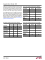
Tables 2 to 4 list circuit parameters that can be verified
during testing of the basic transmitter. The testing reflected
here was done using the components shown in Table 1.
Testing was conducted with Tx and Rx coils with gaps
of 4.5mm, 7.5mm and 10.5mm. Figure 8 shows battery charger power curves with respect to transmit and
receive coil separation and coil center-to-center offset.
Figure 9 shows a typical charge profile with this wireless
power configuration. Actual data will vary with component
tolerance and specific setup. Demo Board design files
and documentation can be found here: www.linear.com/
product/LTC4120#demoboards
Table 3. Basic Transmitter Circuit Parameters (7.5mm Gap)
SPECIFICATION
Operational Frequency
WITHOUT
RECEIVER
(STANDBY)
WITH
RECEIVER
(NO LOAD)
WITH
RECEIVER
(1.58W LOAD)
130.5kHz
128.7kHz
128.9kHz
Input Voltage
4.99V
4.99V
4.95V
Input Current
0.15A
0.173A
0.676A
RMS Value of Tx
Output AC Voltage
10.9V
10.8V
Peak Value of Tx
Output AC Voltage
15.2V
Receiver Output DC
Voltage
SPECIFICATION
Operational Frequency
Standby Loss
Efficiency
WITH RECEIVER
(1.535W LOAD)
129.5kHz
128.8kHz
Input Voltage
4.99V
4.96V
Input Current
0.154A
0.602A
RMS Value of Tx
Output AC Voltage
10.9V
10.5V
Peak Value of Tx
Output AC Voltage
15.2V
15.2V
Receiver Output DC
Voltage
23.9V
17.5V
0.768W
N/A
N/A
51.4%
Standby Loss
Efficiency
Table 2.Basic Transmitter Circuit Parameters (4.5mm Gap)
WITH RECEIVER
(NO LOAD)
Table 4. Basic Transmitter Circuit Parameters (10.5mm Gap)
SPECIFICATION
Operational Frequency
WITH RECEIVER
(NO LOAD)
WITH RECEIVER
(1.53W LOAD)
130.2kHz
128.8kHz
Input Voltage
4.99V
4.95V
Input Current
0.156A
0.658A
10.4V
RMS Value of Tx
Output AC Voltage
10.8V
10.5V
15.2V
15.2V
Peak Value of Tx
Output AC Voltage
15.2V
15.2V
N/A
34.9V
27V
Receiver Output
DC Voltage
17.4V
13.9V
0.75W
0.873W
N/A
Standby Loss
0.77W
N/A
N/A
N/A
47.1%
N/A
46.9%
Efficiency
an138fb
AN138-6