1
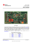
TLC3578EVM Family User’s Guide August 2003 Data Acquisition−Digital/Analog Converters SLAU110 IMPORTANT NOTICE Texas Instruments Incorporated and its subsidiaries (TI) reserve the right to make corrections, modifications, enhancements, improvements, and other changes to its products and services at any time and to discontinue any product or service without notice. Customers should obtain the latest relevant information before placing orders and should verify that such information is current and complete. All products are sold subject to TI’s terms and conditions of sale supplied at the time of order acknowledgment. TI warrants performance of its hardware products to the specifications applicable at the time of sale in accordance with TI’s standard warranty. Testing and other quality control techniques are used to the extent TI deems necessary to support this warranty. Except where mandated by government requirements, testing of all parameters of each product is not necessarily performed. TI assumes no liability for applications assistance or customer product design. Customers are responsible for their products and applications using TI components. To minimize the risks associated with customer products and applications, customers should provide adequate design and operating safeguards. TI does not warrant or represent that any license, either express or implied, is granted under any TI patent right, copyright, mask work right, or other TI intellectual property right relating to any combination, machine, or process in which TI products or services are used. Information published by TI regarding third−party products or services does not constitute a license from TI to use such products or services or a warranty or endorsement thereof. Use of such information may require a license from a third party under the patents or other intellectual property of the third party, or a license from TI under the patents or other intellectual property of TI. Reproduction of information in TI data books or data sheets is permissible only if reproduction is without alteration and is accompanied by all associated warranties, conditions, limitations, and notices. Reproduction of this information with alteration is an unfair and deceptive business practice. TI is not responsible or liable for such altered documentation. Resale of TI products or services with statements different from or beyond the parameters stated by TI for that product or service voids all express and any implied warranties for the associated TI product or service and is an unfair and deceptive business practice. TI is not responsible or liable for any such statements. Following are URLs where you can obtain information on other Texas Instruments products & application solutions: Products Amplifiers Applications amplifier.ti.com Audio www.ti.com/audio Data Converters dataconverter.ti.com Automotive www.ti.com/automotive DSP dsp.ti.com Broadband www.ti.com/broadband Interface interface.ti.com Digital Control www.ti.com/digitalcontrol Logic logic.ti.com Military www.ti.com/military Power Mgmt power.ti.com Optical Networking www.ti.com/opticalnetwork Microcontrollers microcontroller.ti.com Secruity www.ti.com/security Telephony www.ti.com/telephony Video & Imaging www.ti.com/video Wireless www.ti.com/wireless Mailing Address: Texas Instruments Post Office Box 655303 Dallas, Texas 75265 Copyright 2003, Texas Instruments Incorporated EVM IMPORTANT NOTICE Texas Instruments (TI) provides the enclosed product(s) under the following conditions: This evaluation kit being sold by TI is intended for use for ENGINEERING DEVELOPMENT OR EVALUATION PURPOSES ONLY and is not considered by TI to be fit for commercial use. As such, the goods being provided may not be complete in terms of required design-, marketing-, and/or manufacturing-related protective considerations, including product safety measures typically found in the end product incorporating the goods. As a prototype, this product does not fall within the scope of the European Union directive on electromagnetic compatibility and therefore may not meet the technical requirements of the directive. Should this evaluation kit not meet the specifications indicated in the EVM User’s Guide, the kit may be returned within 30 days from the date of delivery for a full refund. THE FOREGOING WARRANTY IS THE EXCLUSIVE WARRANTY MADE BY SELLER TO BUYER AND IS IN LIEU OF ALL OTHER WARRANTIES, EXPRESSED, IMPLIED, OR STATUTORY, INCLUDING ANY WARRANTY OF MERCHANTABILITY OR FITNESS FOR ANY PARTICULAR PURPOSE. The user assumes all responsibility and liability for proper and safe handling of the goods. Further, the user indemnifies TI from all claims arising from the handling or use of the goods. Please be aware that the products received may not be regulatory compliant or agency certified (FCC, UL, CE, etc.). Due to the open construction of the product, it is the user’s responsibility to take any and all appropriate precautions with regard to electrostatic discharge. EXCEPT TO THE EXTENT OF THE INDEMNITY SET FORTH ABOVE, NEITHER PARTY SHALL BE LIABLE TO THE OTHER FOR ANY INDIRECT, SPECIAL, INCIDENTAL, OR CONSEQUENTIAL DAMAGES. TI currently deals with a variety of customers for products, and therefore our arrangement with the user is not exclusive. TI assumes no liability for applications assistance, customer product design, software performance, or infringement of patents or services described herein. Please read the EVM User’s Guide and, specifically, the EVM Warnings and Restrictions notice in the EVM User’s Guide prior to handling the product. This notice contains important safety information about temperatures and voltages. For further safety concerns, please contact the TI application engineer. Persons handling the product must have electronics training and observe good laboratory practice standards. No license is granted under any patent right or other intellectual property right of TI covering or relating to any machine, process, or combination in which such TI products or services might be or are used. Mailing Address: Texas Instruments Post Office Box 655303 Dallas, Texas 75265 Copyright 2003, Texas Instruments Incorporated EVM WARNINGS AND RESTRICTIONS It is important to operate this EVM within the input voltage range of 15 V. Exceeding the specified input range may cause unexpected operation and/or irreversible damage to the EVM. If there are questions concerning the input range, please contact a TI field representative prior to connecting the input power. Applying loads outside of the specified output range may result in unintended operation and/or possible permanent damage to the EVM. Please consult the EVM User’s Guide prior to connecting any load to the EVM output. If there is uncertainty as to the load specification, please contact a TI field representative. During normal operation, some circuit components may have case temperatures greater than 60°C. The EVM is designed to operate properly with certain components above 60°C as long as the input and output ranges are maintained. These components include but are not limited to linear regulators, switching transistors, pass transistors, and current sense resistors. These types of devices can be identified using the EVM schematic located in the EVM User’s Guide. When placing measurement probes near these devices during operation, please be aware that these devices may be very warm to the touch. Mailing Address: Texas Instruments Post Office Box 655303 Dallas, Texas 75265 Copyright 2003, Texas Instruments Incorporated How to Use This Manual Preface Read This First About This Manual This user’s guide describes the characteristics, operation, and use of the following evaluation boards: - TLC3578 EVM Bipolar-Input, 8-channel 14-bit serial analog-to-digital converter - TLC3574 EVM Bipolar-Input, 4-channel 14-bit serial analog-to-digital converter - TLC3548 EVM Unipolar-Input, 8-channel 14-bit serial analog-to-digital converter - TLC3544 EVM Unipolar-Input, 4-channel 14-bit serial analog-to-digital converter - TLC2578 EVM Bipolar-Input, 8-channel 12-bit serial analog-to-digital converter - TLC2574 EVM Bipolar-Input, 4-channel 12-bit serial analog-to-digital converter A complete circuit description as well as schematic diagram and bill of materials is included. Contact the Product Information Center or e-mail [email protected] for questions regarding this EVM. How to Use This Manual This document contains the following chapters: - Chapter 1—EVM Overview - Chapter 2—Analog Interface - Chapter 3—Digital Interface - Chapter 4—Power Supply - Chapter 5—Getting the Most From Your EVM - Chapter 6—Bill of Materials, Board Layouts, and Schematic v Trademarks FCC Warning This equipment is intended for use in a laboratory test environment only. It generates, uses, and can radiate radio frequency energy and has not been tested for compliance with the limits of computing devices pursuant to subpart J of part 15 of FCC rules, which are designed to provide reasonable protection against radio frequency interference. Operation of this equipment in other environments may cause interference with radio communications, in which case the user at his own expense will be required to take whatever measures may be required to correct this interference. Trademarks TI logo is a trademark of Texas Instruments. Related Documentation From Texas Instruments To obtain a copy of any of the following TI documents, call the Texas Instruments Literature Response Center at (800) 477−8924 or the Product Information Center (PIC) at (972) 644−5580. When ordering, please identify this booklet by its title and literature number. Updated documents can also be obtained through our website at www.ti.com. Data Sheets TLC3578 TLC3574 TLC2578 TLC2574 TLC3548 TLC3544 OPA132 REF3040 REF3033 vi Literature Number SLAS262 SLAS266 PDS1309 SBVS032 Contents Contents 1 EVM Overview . . . . . . . . . . . . . . . . . . . . . . . . . . . . . . . . . . . . . . . . . . . . . . . . . . . . . . . . . . . . . . . . . . . 1-1 1.1 Features . . . . . . . . . . . . . . . . . . . . . . . . . . . . . . . . . . . . . . . . . . . . . . . . . . . . . . . . . . . . . . . . . . 1-2 2 Analog Interface . . . . . . . . . . . . . . . . . . . . . . . . . . . . . . . . . . . . . . . . . . . . . . . . . . . . . . . . . . . . . . . . . 2.1 Analog Interface Block Diagram . . . . . . . . . . . . . . . . . . . . . . . . . . . . . . . . . . . . . . . . . . . . . . 2.2 Signal Conditioning . . . . . . . . . . . . . . . . . . . . . . . . . . . . . . . . . . . . . . . . . . . . . . . . . . . . . . . . . 2.3 Single Supply Operation . . . . . . . . . . . . . . . . . . . . . . . . . . . . . . . . . . . . . . . . . . . . . . . . . . . . . 2.4 Physical Pinout Description . . . . . . . . . . . . . . . . . . . . . . . . . . . . . . . . . . . . . . . . . . . . . . . . . . 2.5 Reference Voltage . . . . . . . . . . . . . . . . . . . . . . . . . . . . . . . . . . . . . . . . . . . . . . . . . . . . . . . . . . 2.6 Configuration Options . . . . . . . . . . . . . . . . . . . . . . . . . . . . . . . . . . . . . . . . . . . . . . . . . . . . . . . 3 Digital Interface . . . . . . . . . . . . . . . . . . . . . . . . . . . . . . . . . . . . . . . . . . . . . . . . . . . . . . . . . . . . . . . . . 3-1 3.1 Physical Pinout Description . . . . . . . . . . . . . . . . . . . . . . . . . . . . . . . . . . . . . . . . . . . . . . . . . . 3-2 4 Power Supply . . . . . . . . . . . . . . . . . . . . . . . . . . . . . . . . . . . . . . . . . . . . . . . . . . . . . . . . . . . . . . . . . . . 4-1 5 Getting the Most From Your EVM . . . . . . . . . . . . . . . . . . . . . . . . . . . . . . . . . . . . . . . . . . . . . . . . . 5.1 Additional Hardware Options . . . . . . . . . . . . . . . . . . . . . . . . . . . . . . . . . . . . . . . . . . . . . . . . . 5.1.1 Stand-Alone EVM . . . . . . . . . . . . . . . . . . . . . . . . . . . . . . . . . . . . . . . . . . . . . . . . . . . 5.1.2 DSP Interface . . . . . . . . . . . . . . . . . . . . . . . . . . . . . . . . . . . . . . . . . . . . . . . . . . . . . . . 5.1.3 MSP430 Microcontroller interface . . . . . . . . . . . . . . . . . . . . . . . . . . . . . . . . . . . . . . 5-1 5-2 5-2 5-2 5-3 6 Bill of Materials, Board Layouts, and Schematic . . . . . . . . . . . . . . . . . . . . . . . . . . . . . . . . . . . 6.1 Bill of Materials for EVM . . . . . . . . . . . . . . . . . . . . . . . . . . . . . . . . . . . . . . . . . . . . . . . . . . . . . 6.2 Board Layouts . . . . . . . . . . . . . . . . . . . . . . . . . . . . . . . . . . . . . . . . . . . . . . . . . . . . . . . . . . . . . 6.3 EVM Schematic . . . . . . . . . . . . . . . . . . . . . . . . . . . . . . . . . . . . . . . . . . . . . . . . . . . . . . . . . . . . 6-1 6-2 6-4 6-7 2-1 2-2 2-2 2-2 2-3 2-3 2-4 vii Contents Figures 2−1 5−1 5−2 6−1 6−2 6−3 6−4 Block Diagram . . . . . . . . . . . . . . . . . . . . . . . . . . . . . . . . . . . . . . . . . . . . . . . . . . . . . . . . . . . . . . . . EVM Selection . . . . . . . . . . . . . . . . . . . . . . . . . . . . . . . . . . . . . . . . . . . . . . . . . . . . . . . . . . . . . . . . DSK-To-EVM Stackup Diagram . . . . . . . . . . . . . . . . . . . . . . . . . . . . . . . . . . . . . . . . . . . . . . . . . Top Layer . . . . . . . . . . . . . . . . . . . . . . . . . . . . . . . . . . . . . . . . . . . . . . . . . . . . . . . . . . . . . . . . . . . . Internal Plane 1 . . . . . . . . . . . . . . . . . . . . . . . . . . . . . . . . . . . . . . . . . . . . . . . . . . . . . . . . . . . . . . . Internal Plane 2 . . . . . . . . . . . . . . . . . . . . . . . . . . . . . . . . . . . . . . . . . . . . . . . . . . . . . . . . . . . . . . . Bottom Layer (Mirrored) . . . . . . . . . . . . . . . . . . . . . . . . . . . . . . . . . . . . . . . . . . . . . . . . . . . . . . . . 2-2 5-3 5-3 6-4 6-5 6-5 6-6 Tables 2−1 2−2 2−3 3−1 4−1 viii Analog Input Pinout Description . . . . . . . . . . . . . . . . . . . . . . . . . . . . . . . . . . . . . . . . . . . . . . . . . ADC Reference Voltage . . . . . . . . . . . . . . . . . . . . . . . . . . . . . . . . . . . . . . . . . . . . . . . . . . . . . . . . Jumper Settings . . . . . . . . . . . . . . . . . . . . . . . . . . . . . . . . . . . . . . . . . . . . . . . . . . . . . . . . . . . . . . Digital Signal Pinout Description . . . . . . . . . . . . . . . . . . . . . . . . . . . . . . . . . . . . . . . . . . . . . . . . Power Connector Pinout Description . . . . . . . . . . . . . . . . . . . . . . . . . . . . . . . . . . . . . . . . . . . . . 2-3 2-3 2-4 3-2 4-1 Chapter 1 EVM Overview Each evaluation board is based on the equivalent ADC. All ADCs use a synchronous serial interface which can be simply interfaced to many microcontrollers using the SPI protocol. Each EVM also incorporates a stable voltage reference, and operational amplifier to ensure a low-noise voltage reference for the ADC. Topic 1.1 Page Features . . . . . . . . . . . . . . . . . . . . . . . . . . . . . . . . . . . . . . . . . . . . . . . . . . . . . 1-2 EVM Overview 1-1 Features 1.1 Features - Evaluation board featuring one of the following: J TLC3578 ADC (order TLC3578 EVM) J TLC3574 ADC (order TLC3574 EVM) J TLC3548 ADC (order TLC3548 EVM) J TLC3544 ADC (order TLC3544 EVM) J TLC2578 ADC (order TLC2578 EVM) J TLC2574 ADC (order TLC2574 EVM) - Onboard reference, with recommended buffer circuitry - Suggested signal conditioning circuitry for 1 channel only 1-2 Chapter 2 Analog Interface Topic Page 2.1 Analog Interface Block Diagram . . . . . . . . . . . . . . . . . . . . . . . . . . . . . . . . 2-2 2.2 Signal Conditioning . . . . . . . . . . . . . . . . . . . . . . . . . . . . . . . . . . . . . . . . . . . 2-2 2.3 Single Supply Operation . . . . . . . . . . . . . . . . . . . . . . . . . . . . . . . . . . . . . . . 2-2 2.4 Physical Pinout Description . . . . . . . . . . . . . . . . . . . . . . . . . . . . . . . . . . . 2-3 2.5 ADC Reference Voltage . . . . . . . . . . . . . . . . . . . . . . . . . . . . . . . . . . . . . . . . 2-3 2.6 Configuration Options . . . . . . . . . . . . . . . . . . . . . . . . . . . . . . . . . . . . . . . . . 2-4 Analog Interface 2-1 Analog Interface Block Diagram 2.1 Analog Interface Block Diagram A block diagram for the analog interface of the EVM is shown in Figure 2−1. Figure 2−1. Block Diagram P1 / J1 Signal Conditioning TLC3578 TLC3574 TLC3548 TLC3544 TLC2578 TLC2574 The channels are arranged to comply with the EVM standard developed for data converters. This standard defines eight channels of analog I/O on each EVM module. 2.2 Signal Conditioning The facility exists for the signal connected to channel 0 to be conditioned via an operational amplifier. The amplifier present on the EVM operates from a dual power supply and is configured with a gain of +1. If signal conditioning is not required, it can easily be bypassed via a shorting bar. 2.3 Single Supply Operation Should the user wish to operate the amplifier from a single suply rail, this is also possible by simply removing the dual supply amplifier and replacing it with a suitable single supply alternative, for example the OPA353. The suggested procedure is detailed below: - Carefully desolder amplifier, U1 - Replace with a suitable single-supply alternative, for example TI part num- ber OPA353UA - Install appropriate resistor at R9 - Install appropriate capacitor at C11 - Install shorting bar at W1 2-2 Physical Pinout Description 2.4 Physical Pinout Description Samtec part numbers SSW-110-22-F-D-VS-K and TSM-110-01-T-DV-P provide a convenient 10-pin dual row header/socket combination at P1. This header/socket provides access to the analog input pins of the TLV2553/6. Consult Samtec at www.samtec.com or 1−800−SAMTEC−9 for a variety of mating connector options. Table 2−1. Analog Input Pinout Description Pin Number Signal Description J1.2 CH0 Channel 0 input, can be direct from P1/J1 connector or through Op-Amp P1.4 J1.4 CH1 Channel 1 input, direct from P1/J1 connector P1.6 J1.6 CH2 Channel 2 input, direct from P1/J1 connector P1.8 J1.8 CH3 Channel 3 input, direct from P1/J1 connector P1.10 J1.10 CH4 Channel 4 input, direct from P1/J1 connector P1.12 J1.12 CH5 Channel 5 input, direct from P1/J1 connector P1.14 J1.14 CH6 Channel 6 input, direct from P1/J1 connector P1.16 J1.16 CH7 Channel 7 input, direct from P1/J1 connector P1.18 J1.18 REF− External Reference negative input P1.20 J1.20 REF+ External Reference positive input Header Socket P1.2 2.5 Reference Voltage The accuracy of conversion from a SAR ADC depends directly upon the accuracy of the reference voltage. It is very important, therefore, that the reference be stable, accurate and low drift. The ADC reference pin presents a dynamic capacitive load to the amplifier. The voltage supplied to the ADC must be capable of driving this dynamic load properly, ensuring that the reference remain stable regardless of load. The bipolar and unipolar devices are specified to use a different voltage for the reference pin. Table 2−2. ADC Reference Voltage ADC Reference Voltage Bipolar input TLC3578 3.3 V TLC3574 3.3 V TLC2578 3.3 V TLC2574 3.3 V Unipolar input TLC3548 4.096 V TLC3544 4.096 V Analog Interface 2-3 Configuration Options 2.6 Configuration Options There are a number of options available via shorting jumpers. These are detailed below: Table 2−3. Jumper Settings Reference Designator Factory Set Condition Position Description Optional Position W1 Single supply operation 1−2 Not installed W2 Select negative supply for op amp −Vs AGND (0 V) W3 Select positive supply for op amp +Vs +Vcc (5 V) W4 Select signal source for channel 0 Signal is via op amp Signal is directly from P1.2 W5 Select positive voltage reference Onboard reference Reference via P1.18 W6 Select digital power 5V 3.3 V W7 Select negative voltage reference Onboard reference Reference via P1.20 W8 CSTART, initiate manual conversion Disabled Enabled W9 W10 FS mode Device always selected Disabled Disabled Enabled Enabled 2-4 2−3 Chapter 3 Digital Interface The digital interface for the EVM is simply the appropriate digital signals from the ADC routed and presented to the 20-pin digital interface connector. Topic 3.1 Page Physical Pinout Description . . . . . . . . . . . . . . . . . . . . . . . . . . . . . . . . . . . 3-2 Digital Interface 3-1 Physical Pinout Description 3.1 Physical Pinout Description The EVM is designed for easy interfacing to multiple platforms. Samtec part numbers SSW-110-22-F-D-VS-K and TSM-110-01-T-DV-P provide a convenient 10-pin dual row header/socket combination. This header/socket combination provides access to the digital control and serial data pins of the EVM. Consult Samtec at www.samtec.com or 1−800−SAMTEC−9 for a variety of mating connector options. Table 3−1. Digital Signal Pinout Description Pin Number Header † Signal Socket Description P3.1 J3.1 CS Chip select selects the device for data transfer. P3.3 J3.3 SCLK/CLKX Data transfer clock P3.5 J3.5 Reserved P3.7 J3.7 FSX P3.9 J3.9 FSR P3.11 J3.11 SDI Serial data into the device P3.13 J3.13 SDO Serial data out of the device P3.15 J3.15 EOC or INT/EOC† Selects either EOC or INT − see data sheet for details. P3.17 J3.17 Reserved P3.19 J3.19 CSTART Programmable as either EOC or INT 3-2 Control the beginning of a conversion Chapter 4 Power Supply The EVM accepts four power supplies. - A dual ± Vs dc supply for the dual-supply op-amps. - A single 5.0 V dc supply for the analog section of the ADC. - A single 3.3 V to 5 V dc supply for the digital section of the ADC. There are two ways to provide these voltages. - Hook-up the test points on the EVM. The test points are clearly labeled +Vdd (3.3 V to 5 V), +5VA, +Vs (up to 18 V depending upon the amplifiers) and –Vs (up to –18 V depending upon the amplifiers). - Use the power connector P5/J5 and derive the voltages elsewhere. The pinout for this connector is shown in Table 4−1. Table 4−1. Power Connector Pinout Description Signal P5/J5 Pin Number Signal +VA 1 2 −VA +5VA 3 4 −5VA AGND 5 6 DGND +1.8VD 7 8 VD1 +3.3VD 9 10 +5VD Power Supply 4-1 4-2 Chapter 5 Getting the Most From Your EVM A wide range of prototyping options and software solutions are available from TI, and offer additional flexibility, reducing your time-to-market. Hardware and software offerings from TI help you easily get from concept to hardware and software prototype. Topic 5.1 Page Additional Hardware Options . . . . . . . . . . . . . . . . . . . . . . . . . . . . . . . . . . 5-2 Getting the Most From Your EVM 5-1 Additional Hardware Options 5.1 Additional Hardware Options In general there are three hardware directions that the user can take with the EVM. 5.1.1 Stand-Alone EVM The EVM can be used on its own. Using the EVM in this manner obliges the user to provide a custom digital interface between the EVM and a host system. Users are entirely responsible for ensuring proper timing requirements are met in addition to providing any glue logic necessary. Users must also provide the necessary analog interface and supply power to the EVM. 5.1.2 DSP Interface Depending upon the DSP that the user chooses, there are a number of TI DSKs available. DSKs are DSP Starter Kits, and provide users with a DSP starter system. They contain all the necessary hardware and software to quickly begin prototype construction. For example, the TMS320C6711 DSP starter kit includes the DSK hardware, a parallel port cable to connect to a PC, a 5-V universal power supply, and a Code Composer Studio CD-ROM containing all the necessary software. Each family of DSKs provides different physical interface options. These interface options enable address, data, and control signals to be decoded and used by mezzanine-level cards (such as EVMs). To connect this EVM to any DSK requires selection of the correct interface card. Generally the procedure is outlined below. - Select the DSP you wish to use. - Select the appropriate DSK. - Select the suitable interface card. As an example, assume that the user wishes to use the TLC3578 EVM with the TMS320C6711 DSP, the steps that should be taken are shown below following a side-elevation of the boards required. 5-2 Additional Hardware Options Figure 5−1. EVM Selection TMS320C2000 Interface Card TLC3574 EVM TMS320C6711 DSP TMS320C3000 Interface Card TMS320C6711 DSK TLC3578 EVM TLC3544 EVM TMS320C5K / 6K Interface Card TLC3548 EVM 1. Select DSP 2. Select DSK 3. Select Interface Card. TLC3578 EVM TLC3574 EVM Figure 5−2. DSK-To-EVM Stackup Diagram C5K / 6K Interface Card Evaluation Module Site Amplifier Site C5K / 6K Interface Card DSK 80-Pin DSK Common Connector 5.1.3 MSP430 Microcontroller interface TI also offer a range of low-power microcontrollers that have an SPI interface. You can check-out these devices and order evaluation modules at www.ti.com A microcomputer evaluation board exists, featuring the MSP430F449 that also enables the ADC EVMs to be connected directly. The HPA449 evaluation board, available from www.softbaugh.com includes the following features: Getting the Most From Your EVM Softbaugh 5-3 5-4 Chapter 6 Bill of Materials, Board Layouts, and Schematic This chapter contains the EVM bill of materials, board layouts and schematics. Topic Page 6.1 Bill of Materials for EVM . . . . . . . . . . . . . . . . . . . . . . . . . . . . . . . . . . . . . . . 6-2 6.2 Board Layouts . . . . . . . . . . . . . . . . . . . . . . . . . . . . . . . . . . . . . . . . . . . . . . . . 6-3 6.3 EVM Schematic . . . . . . . . . . . . . . . . . . . . . . . . . . . . . . . . . . . . . . . . . . . . . . . 6-6 Bill of Materials, Board Layouts, and Schematic 6-1 Bill of Materials for EVM 6.1 Bill of Materials for EVM Item no. 1 Qty Value Ref Des 1 0R R19 2 2 0R R8, R17 3 1 10R R15 4 9 33R 5 4 100R 6 2 10 KΩ R1, R2, R3, R4, R5, R6, R7, R12, R13 R10, R11, R20, R21 R16, R18 7 1 10 pF 8 8 0.1 µF 9 8 27 nF 10 1 1 µF 11 1 10 µF 12 4 10 µF 13 14 2 8 15 Description Part number Panasonic ERJ−2GE0R00X Panasonic ERJ−8GEY0R00V Panasonic ERJ−8GEYJ100V Panasonic ERJ−8GEYJ330V Panasonic ERJ−8GEYJ101V Panasonic ERJ−8GEYJ103V Panasonic ECJ−2VC1H100D Panasonic ECJ−2VB1E104K Panasonic ECJ−2VB1H273K Panasonic ECJ−2YB1A105K Panasonic ECS−T1CX106R Panasonic ECE−V1CA100SR Samtec Samtec TSW−102−07−L−S TSW−103−07−L−S 1 Resistor, 100−Ω 1/8 W 5% 1206 SMD Resistor, 10−kΩ, 1/8 W 5% 1206 SMD C3 Capacitor, 10−pF 50 V Ceramic chip, 0805 SMD C1, C13, C15, Capacitor, .1−µF 25 V Ceramic, X7R 0805 C16, C20, C22, C23, C24 Capacitor, 27000−pF 50 V, C4, C5, C6, Ceramic, X7R 0805 C7, C8, C9, C10, C14 C18 Capacitor, 1−ìF 10 V J Ceramic X5R 0805 C17 Capacitor, 10−µF 16 V tantalum, TE series C2 C12 C19 Capacitor, 10−µF 16 V, C21 VS electrolytic, SMD W1, W10 2−pin header W2, W3, W4, 3−Pin header W5, W6, W7, W8, W9 P5 10−Pin header Samtec 16 1 J5 10−Socket strip Samtec 17 4 P1 P2 P3 P4 20−Pin header Samtec 18 4 J1 J2 J3 J4 20−Socket strip Samtec 19 3 2 OPA132UA 1 REF3033 Texas Instruments Texas Instruments OPA132UA 21 Fair−Rite SM beads #24−−44447 IC, FET−input op amp, 8−SOIC IC voltage reference, 3.33−V LP SOT−23 Fair-Rite 20 FB1, FB2, FB3 U1, U3 TSM−105−01−T−DV− P SSW−105−22−F−D− VS−K TSM−110−01−T−DV− P SSW−110−22−F−D− VS−K 2744044447 IC, voltage reference, 4.096−V, LP SOT−23 Texas Instruments REF3040AIDBZT Contingent on Item 22 6-2 REF3040 U2 U2 Resistor, 0−Ω 1/16 W 5% 0402 SMD Resistor, 0−Ω 1/8 W 5% 1206 SMD Resistor 10−Ω 1/8 W 5% 1206 SMD Resistor, 33−Ω 1/8 W 5% 1206 SMD Vendor REF3033AIDBZT Bill of Materials for EVM 22 1 TLC3578 U4 Alternate TLC3574 U4 Alternate TLC3548 U4 Alternate TLC3544 U4 Alternate TLC2578 U4 Alternate TLC2574 U4 23 2 24 1 25 4 TP_.025 26 2 1 TP_turret Not Installed Not Installed Not Installed 1 1 SN74LVC1 G07 IC, A/D 8−CH, 14−BIT, LP 24−TSSOP IC, A/D, 4−Ch, 14−bit LP 20−TSSOP IC, Unipolar A/D 8−CH 24−SOIC IC, Unipolar A/D 4−CH 20−SOIC IC, Serial out A/D 8−CH 24−SOIC IC, Serial out A/D 4−CH 20−TSSOP Single IC buffer driver with open drain o/p TLC3578 Rev A PWB +5VA, +VA, −VA, Vdd AGND, DGND R14 Test Point − Single .025” Pin Turret terminal test point * Texas Instruments Texas Instruments Texas Instruments Texas Instruments Texas Instruments Texas Instruments Texas Instruments Texas Instruments Keystone Electronics Cambion * C11 * * * R9 * * * U5, U6 Bill of Materials, Board Layouts, and Schematic TLC3578IPW TLC3574IPW TLC3548IPW TLC3544IPW TLC2578IPW TLC2574IPW SN74LVC1G07DBVR 6448024 5000 180−7337−02−05 * 6-3 Board Layouts 6.2 Board Layouts Figure 6−1. Top Layer 6-4 Board Layouts Figure 6−2. Internal Plane 1 Figure 6−3. Internal Plane 2 Bill of Materials, Board Layouts, and Schematic 6-5 Board Layouts Figure 6−4. Bottom Layer (Mirrored) 6-6 EVM Schematic 6.3 EVM Schematic The EVM schematic is a PDF attachment following this page. Bill of Materials, Board Layouts, and Schematic 6-7 1 2 3 4 5 6 Revision History REV ECN Number Approved D D P1 C P3 TLC3578 TLC3578.sch 1 2 3 4 5 6 7 8 9 10 11 12 13 14 15 16 17 18 19 20 CH0 CS* CH1 CLKX CH2 R17 CH3 0R CH4 FSX FSR CH5 DATA_IN CH6 B_DATA_OUT CH7 B_INT*/EOC REFREF+ GPIO_1 1 2 3 4 5 6 7 8 9 10 11 12 13 14 15 16 17 18 19 20 C DGND AGND B B PWR & REF PWR & REF.sch ti A A 12500 TI Boulevard. Dallas, Texas 75243 Title: TLC3578 EVM Block Diagram Engineer: Joe Purvis Drawn By: FILE: 1 2 3 4 5 DOCUMENTCONTROL # REV: 6448025 Joe Purvis DATE: TLC3578 EVM Block Diagram 21-Aug-2003 SIZE: 6 SHEET: 1 OF: 2 3 1 2 3 4 5 6 Revision History REV ECN Number Approved GPIO_1 FSX DVdd FS CS* W10 CSTART* W8 DVdd D W1 C11 R9 W9 D R18 DGND Not Installed 10K Not Installed R16 10K R8 AGND 0R CH0 Amplifier +Supply +5V_s W4 Amplifier -Supply 11 12 13 R7 14 33R CH6 C10 27nF R2 15 33R 16 C5 27nF AGND 7 AIN0 CS* AIN1 AIN2 SCLK AIN3 SDI AIN4 CSTART* INT* / EOC 33R C 100R CLKX U6A DATA_IN 5 DATA_OUT 24 CSTART* 4 INT*/EOC 2 2 A A B_DATA_OUT 4 Y SN74LVC1G07 B_INT*/EOC 4 Y DGND AGND C20 REF_P REFM 20 REF_M TLC3578 0.1uF 6 C4 27nF 19 COMP AGND 33R R5 R13 BCLK R21 100R SN74LVC1G07 R1 AGND DVdd AIN7 22 CH7 FS U5A REFP 21 C9 27nF CS* 2 3 AIN6 18 R6 8 1 SDO AIN5 DVdd R20 FS AGND 33R CH3 DVdd 9 AVdd AGND 10 CH2 AVdd U4 +In C CH1 23 17 6 4 3 C14 27nF U1 -In Output CH0 DVdd 33R 7 2 R12 AGND 33R B B C8 27nF AGND DGND AGND CH4 R4 33R C7 27nF AGND CH5 REF+ R3 W5 33R REF_P C6 27nF C15 C18 + C17 1uF 10uF AGND 0.1uF REF_M VREF+ REFW7 ti A AGND 12500 TI Boulevard. Dallas, Texas 75243 Title: Engineer: Joe Purvis Drawn By: 1 2 3 4 5 A FILE: TLC3578 DOCUMENTCONTROL # REV: 6448025 Joe Purvis TLC3578.sch DATE: 21-Aug-2003 SIZE: 6 SHEET: 2 OF: 2 3 1 2 3 4 5 6 Revision History REV U5B 1 NC Approved U6B Vcc 5 DVdd 1 C23 DGND3 ECN Number GND DGND3 0.1uF NC 5 Vcc DVdd C24 GND 0.1uF +5VA D SN74LVC1G07 D SN74LVC1G07 +5VA C16 AGND +5V_s + C19 10uF 0.1uF +VA FB3 W3 Amplifier +Supply AGND +VA FB2 +V_s FB1 -V_s +3.3V_D C13 DVdd 9 7 5 3 1 Vdd W6 R15 P5 AGND 10 8 6 4 2 10R + C12 10uF 0.1uF -VA +5V_D + C21 10uF 0.1uF C1 C2 10uF + C22 DGND -VA 0.1uF W2 Amplifier -Supply AGND C C AGND DGND R11 R19 100R 0R C3 R14 Not Installed 10pF AGND DGND Amplifier +Supply DGND 7 AGND 2 U3 -In U2 +5V_s 1 IN 2 OUT 3 R10 6 VREF+ 100R +In B 4 B Output 3 P2 GND P4 Amplifier -Supply REF3040 1 2 1 2 3 4 3 4 5 6 5 6 7 8 7 8 9 10 9 10 11 12 11 12 13 14 13 14 15 16 15 16 17 18 17 18 19 20 19 20 AGND ti A A 12500 TI Boulevard. Dallas, Texas 75243 Title: Engineer: Joe Purvis Drawn By: 1 2 3 4 5 FILE: TLC3578 EVM Power & Reference DOCUMENTCONTROL # REV: 6448025 Joe Purvis PWR & REF.sch DATE: 21-Aug-2003 SIZE: 6 SHEET: 3 OF: 2 3