1
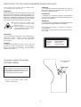
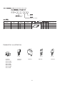
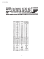
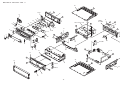
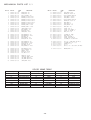
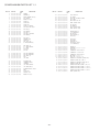
CDC-X207 YU
CDC-X307 YU
CDC-X407 YU
CDC-X2070 YL
CDC-X3070 YL
CDC-X4010 YL
SERVICE MANUAL
STEREO CAR CD RECEIVER
BASIC CD MECHANISM: TN-CCD1001-113J
S/M Code No. 09-002-422-3R1
RE
VI
SIO
DA
N
TA
• This Service Manual is the “Revision Publishing” and replaces “Simple Manual”
of CDC-X207/ X307/ X407<YU>, (S/M Code No. 09-99B-422-3T1) and
CDC-X2070/ X3070/ X4010<YL>, (S/M Code No. 09-99C-422-3T2).
SPECIFICATIONS
RADIO SECTION
AUDIO SECTION
(FM)
Frequency Range
Max. Power Output
87.5 MHz –108 MHz (100-kHz steps)
87.5 MHz –108 MHz (50-kHz steps)
Usable Sensitivity
12.7 dBf
50 dB Quieting Sensitivity 17.2 dBf
IF Rejection
80 dB
Frequency Response
30 Hz – 15,000 Hz
S/N Ratio
63 dB
Stereo Separation
35 dB at 1 kHz
Alternate Channel Selectivity
70 dB
Capture Ratio
3 dB
(AM)
Frequency Range
530 kHz – 1,710 kHz (10-kHz steps)
531 kHz – 1,602 kHz (9-kHz steps)
30 µV (30 dB)
Usable Sensitivity
Set the frequency increment for your area using the switch on the
bottom of the unit.
(The switch is set at the factory to the 10k position [for the U.S.A.])
CD SECTION
Frequency Response
Dynamic Range
Channel Separation
S/N Ratio
Wow/Flutter
17 Hz – 20 kHz +0/–3 dB
More than 80 dB
More than 65 dB
More than 85 dB
Unmeasurable
45 W x 4 channels
<except CDC-X2070>
35 W x 4 channels <CDC-X2070 only>
TAPE/MD IN input
Input Sensitivity (load impedance)
TAPE/MD IN
500 mV (10 kΩ)<YU>
300 mV (10 kΩ)<YL>
GENERAL
Power Supply Voltage
14.4 V (11 to 16 V allowable),
DC, negative ground
Load Impedance
4Ω
Tone Control
Bass ±10 dB at 100 Hz
Treble ±10 dB at 10 kHz
Preamp Output Voltage (load impedance)
2.2 V (10 kΩ)
Installation Size
182 (W) x 53 (H) x 155 (D) mm
(71/4 (W) x 21/8 (H) x 61/8 (D) inches)
STEERING-WHEEL-MOUNTED REMOTE CONTROL UNIT <CDCX407/4010 only>
Dimensions
approx. 67 (W) x 26 (H) x 27 (D) mm
(23/4 (W) x 11/16 (H) x 11/8 (D) inches)
(excluding holder)
Weight
approx. 38g (1.33 oz.)
(including holder, battery)
• Design and specifications are subject to change without
notice.
ACCESSORIES / PACKAGE LIST
REF. NO.
PART NO.
KANRI
DESCRIPTION
1
1
1
1
2
8A-KC7-902-010
8A-KCG-902-010
8A-KCG-901-010
8A-KCG-903-010
87-B10-141-010
IB,INST,YU,YL (3L,P)
IB,YU(3L) 207<X207>
IB,YU(3L) 307,407<X307,X407>
IB,YL(3L) 4010, 3070, 2070<YL>
NUT,5 TYPE-2
3
4
5
6
7
87-B10-143-010
87-B10-144-010
87-B10-145-010
87-B10-216-010
8Z-KC1-030-010
UT1+5-15 W/O SLOT
W,5.2-10-0.5
W-SPR,5.3-8.5-1.5
U+2.6-4.0 ZINC BLK (BH M2.6)
CASE,DFP -C
8
9
10
11
12
8Z-KC1-231-110
8Z-KC1-232-010
8Z-KC1-235-010
8Z-KC1-244-010
8Z-KC1-250-010
HLDR,HALF -C
KEY,REMOVE -C
HLDR,REAR MTG
S-SCREW,5*6 TH+ TAPPING ST
S-SCREW,HEXAGON
13
8Z-KT1-616-010
CONN ASSY,16P B52
-2-
PROTECTION OF EYES FROM LASER BEAM DURING SERVICING
CAUTION
This set employs laser. Therefore, be sure to follow carefully
the instructions below when servicing.
Use of controls or adjustments or performance of procedures other than those specified herin may result in
hazardous radiation exposure.
WARNING!!
WHEN SERVICING, DO NOT APPROACH THE LASER
EXIT WITH THE EYE TOO CLOSELY. IN CASE IT IS
NECESSARY TO CONFIRM LASER BEAM EMISSION.
BE SURE TO OBSERVE FROM A DISTANCE OF MORE
THAN 30cm FROM THE SURFACE OF THE OBJECTIVE LENS ON THE OPTICAL PICK-UP BLOCK.
ATTENTION
L’utillisation de commandes, réglages ou procédures
autres que ceux spécifiés peut entraîner une dangereuse
exposition aux radiations.
ADVARSEL
s
s
Usynlig laserståling ved åbning, når sikkerhedsafbrydereer
ude af funktion. Undgå udsættelse for stråling.
Caution: Invisible laser radiation when
open and interlocks defeated avoid
exposure to beam.
Advarsel: Usynlig laserståling ved åbning,
når sikkerhedsafbrydere er ude af funktion.
Undgå udsættelse for stråling.
This Compact Disc player is classified as a CLASS 1
LASER product.
The CLASS 1 LASER PRODUCT label is located on the
rear exterior.
VAROITUS!
Laiteen Käyttäminen muulla kuin tässä käyttöohjeessa
mainitulla tavalla saataa altistaa käyt-täjän
turvallisuusluokan 1 ylittävälle näkymättömälle
lasersäteilylle.
CLASS 1
KLASSE 1
LUOKAN 1
KLASS 1
VARNING!
Om apparaten används på annat sätt än vad som
specificeras i denna bruksanvising, kan användaren
utsättas för osynling laserstrålning, som överskrider
gränsen för laserklass 1.
Precaution to replace Optical block
LASER PRODUCT
LASER PRODUKT
LASER LAITE
LASER APPARAT
PICK-UP ASSY
P.C.B
(OPTIMA-720AIE)
Body or clothes electrostatic potential could
ruin laser diode in the optical block. Be sure
ground body and workbench, and use care
the clothes do not touch the diode.
1) After the connection, remove solder
shown in right figure.
-3-
ELETRICAL MAIN PARTS LIST
REF. NO.
PART NO.
KANRI
NO.
DESCRIPTION
REF. NO.
IC
87-A20-446-010
87-A21-319-010
87-A21-488-040
8Z-KT1-622-010
87-A21-562-010
C-IC,LA9241ML
C-IC,LC78622NE
C-IC,LA6556
C-IC,LC75374E
IC,LA4743B
88-KT1-606-080
87-A21-535-030
87-A21-489-030
87-A90-951-010
IC,PST994D
C-IC,LC72358N-9910
C-IC,LC75853NW
RCR UNIT,SBX1971-52<X407>
TRANSISTOR
89-324-122-080
87-A30-289-040
87-A30-288-040
87-A30-287-040
87-026-235-080
TR,2SC2412K
C-TR,2SA1037AK(R)
C-TR,DTC114YKA
C-TR,DTC114TKA
CHIP-TR,DTC114EK
87-026-210-080
87-A30-299-080
87-A30-282-040
87-A30-168-010
89-211-821-080
CHIP-TR,DTC144EK
TR,2SB1326
C-TR,DTA114TKA
TR,2SB1566F
CHIP-TR 2SB1182Q
89-423-953-010
87-A30-301-080
87-A30-449-040
TR,2SD2395F
TR,2SD1862
C-TR,DTA123YKA
87-A40-250-080
87-001-783-080
87-020-331-080
87-A40-624-080
87-A40-523-080
CHIP-DIODE,DAN202K
DIODE,1N4002
CHIP-DIODE,DAN202K
ZENER,MTZJ10A
ZENER,MTZJ9.1B
87-070-136-080
87-017-932-080
87-A40-798-010
87-A40-817-040
ZENER,MTZJ5.1B
ZENER,MTJ6.2B
DIODE,1N5402 (3A/200V)
C-ZENER,STZ6.8N
C101
C102
C103
C106
C107
87-010-178-080
87-010-197-080
87-010-495-040
87-010-322-080
87-010-552-040
CHIP CAP 1000P
CAP, CHIP 0.01 DM
CAP,E 2.2-50 GAS
C-CAP,S 100P-50 CH
CAP,E 22-16 GAS
C108
C109
C110
C111
C112
87-010-322-080
87-010-553-040
87-010-198-080
87-010-553-040
87-010-185-080
C-CAP,S 100P-50 CH
CAP,E 47-16 GAS
CAP, CHIP 0.022
CAP,E 47-16 GAS
C-CAP,S 3900P-50 B
C113
C114
C115
C116
C131
87-010-197-080
87-010-197-080
87-010-196-080
87-010-196-080
87-012-365-080
CAP, CHIP 0.01 DM
CAP, CHIP 0.01 DM
CHIP CAPACITOR,0.1-25
CHIP CAPACITOR,0.1-25
C-CAP,S 0.027-25VBK<YU>
C131
C132
C132
C133
C134
87-010-220-080
87-012-365-080
87-010-220-080
87-012-358-080
87-012-358-080
C-CAP,S
C-CAP,S
C-CAP,S
C-CAP,S
C-CAP,S
C161
C171
C173
C176
C201
87-010-196-080
87-010-197-080
87-010-322-080
87-010-197-080
87-010-553-040
CHIP CAPACITOR,0.1-25
CAP, CHIP 0.01 DM<YU>
C-CAP,S 100P-50 J CH GRM
C-CAP,S 0.01-25 K B<YL>
CAP,E 47-16 GAS
C202
C203
C204
87-010-553-040
87-010-178-080
87-016-669-080
CAP,E 47-16 GAS
CHIP CAP 1000P
C-CAP,S 0.1-25 K B
DIODE
PART NO.
C205
C206
C207
C208
C209
KANRI
NO.
87-A11-606-080
87-010-492-040
87-010-195-080
87-010-176-080
87-010-992-080
DESCRIPTION
C-CAP,S 0.22-25 K B
CAP,E 0.33-50 GAS
C-CAP,S 0.068-25 Z F C2012
C-CAP,S 680P-50 J SL
CAP, CHIP 0.047
C210
C211
C212
C213
C214
87-016-669-080
87-010-498-040
87-010-180-080
87-010-992-080
87-016-669-080
C-CAP,S 0.1-25 K B
CAP,E 10-16 M 5L SRE
C-CER 1500P
CAP, CHIP 0.047
C-CAP,S 0.1-25 K B
C215
C215
C216
C217
C218
87-010-178-080
87-010-182-080
87-A11-606-080
87-016-669-080
87-010-198-080
C-CAP,S 1000P-50 K B C2012<YU>
C-CAP,S 2200P-50 K B C2012<YL>
C-CAP,S 0.22-25 K B
C-CAP,S 0.1-25 K B
CAP, CHIP 0.022
C219
C220
C221
C222
C223
87-012-157-080
87-010-184-080
87-010-322-080
87-010-492-040
87-010-067-040
C-CAP,S 330P-50 CH
CHIP CAPACITOR 3300P(K)
C-CAP,S 100P-50 CH
CAP,E 0.33-50 GAS
CAP,E 0.1-50 5L
C224
C225
C225
C226
C227
87-010-553-040
87-010-805-080
87-010-184-080
87-010-497-040
87-010-555-040
CAP,E 47-16 GAS
C-CAP,S 1-16 Z F<YU>
C-CAP,S 3300P-50 K B C2012<YL>
CAP,E 4.7-35 GAS
CAP,E 100-10 GAS
C228
C229
C230
C231
C232
87-016-669-080
87-010-498-040
87-016-669-080
87-010-555-040
87-016-669-080
CHIP CAPACITOR,0.1-25
CAP,E 10-16 GAS
CHIP CAPACITOR,0.1-25
CAP,E 100-10 GAS
CHIP CAPACITOR,0.1-25
C233
C234
C235
C236
C237
87-010-555-040
87-010-193-080
87-010-992-080
87-010-067-040
87-010-553-040
CAP,E 100-10 GAS
CHIP CAPACITOR,0.033
CAP, CHIP 0.047
CAP,E 0.1-50 5L
CAP,E 47-16 GAS
C238
C240
C250
C250
C251
87-010-197-080
87-016-669-080
87-016-669-080
87-010-805-080
87-010-555-040
CAP, CHIP 0.01 DM
C-CAP,S 0.1-25 K B
CHIP CAPACITOR,0.1-25<YU>
C-CAP,S 1-16 Z F<YL>
CAP,E 100-10 GAS
C256
C258
C259
C261
C262
87-010-186-080
87-010-150-080
87-010-316-080
87-012-156-080
87-016-669-080
CAP,CHIP 4700P
C-CAP,S 6P-50 D CH
C-CAP,S 33P-50 CH
C-CAP,S 220P-50 J CH GRM
C-CAP,S 0.1-25 K B
C263
C264
C265
C266
C267
87-010-555-040
87-010-555-040
87-016-669-080
87-016-669-080
87-010-498-040
CAP,E 100-10 GAS
CAP,E 100-10 GAS
C-CAP,S 0.1-25 K B
C-CAP,S 0.1-25 K B
CAP,E 10-16 GAS
C268
C269
C270
C271
C272
87-010-498-040
87-010-180-080
87-010-180-080
87-010-154-080
87-010-154-080
CAP,E 10-16 GAS
C-CER 1500P
C-CER 1500P
CAP CHIP 10P
CAP CHIP 10P
C273
C274
C280
C281
C282
87-010-494-040
87-010-494-040
87-A10-189-040
87-010-555-040
87-016-669-080
CAP,E 1-50 M 5L SRE
CAP,E 1-50 M 5L SRE
CAP,E 220-10
CAP,E 100-10 GAS
C-CAP,S 0.1-25 K B
C301
C302
C303
C304
C305
87-010-498-040
87-010-498-040
87-010-494-040
87-010-494-040
87-010-184-080
CAP,E 10-16 GAS
CAP,E 10-16 GAS
CAP,E 1-50 GAS
CAP,E 1-50 GAS
CHIP CAPACITOR 3300P(K)
C306
C307
C308
C309
C310
87-010-184-080
87-010-198-080
87-010-198-080
87-010-498-040
87-010-498-040
CHIP CAPACITOR 3300P(K)
CAP, CHIP 0.022
CAP, CHIP 0.022
CAP,E 10-16 GAS
CAP,E 10-16 GAS
MAIN C.B
0.018-25 K B<YL>
0.027-25VBK<YU>
0.018-25 K B<YL>
0.47-10 F Z
0.47-10 F Z
-4-
REF. NO.
PART NO.
C311
C312
C313
C314
C315
KANRI
NO.
87-A11-177-080
87-A11-177-080
87-A11-177-080
87-A11-177-080
87-010-498-040
DESCRIPTION
C832
C835
C836
C881
C882
KANRI
NO.
87-010-494-040
87-010-182-080
87-010-182-080
87-010-182-080
87-010-182-080
C-CAP,S 0.15-16
C-CAP,S 0.15-16
C-CAP,S 0.15-16
C-CAP,S 0.15-16
CAP,E 10-16 GAS
CAP,E 1-50 M 5L SRE
C-CAP,S 2200P-50 K B C2012
C-CAP,S 2200P-50 K B C2012
C-CAP,S 2200P-50 B
C-CAP,S 2200P-50 B
C316
C321
C322
C323
C324
87-010-498-040
87-010-196-080
87-010-555-040
87-010-196-080
87-010-498-040
CAP,E 10-16 GAS
CHIP CAPACITOR,0.1-25
CAP,E 100-10 GAS
CHIP CAPACITOR,0.1-25
CAP,E 10-16 GAS
C883
C884
CON201
CON202
CON851
87-010-182-080
87-010-182-080
87-A60-859-010
87-A60-860-010
88-KTA-603-010
C-CAP,S 2200P-50 B
C-CAP,S 2200P-50 B
CONN,12P TKC-F12X-K1
CONN,14P TKC-F14X-K1
CONN,15P CAM-B68
C331
C332
C333
C334
C351
87-012-358-080
87-012-358-080
87-010-196-080
87-010-196-080
87-010-494-040
C-CAP,S 0.47-10 F Z
C-CAP,S 0.47-10 F Z
C-CAP,S 0.1-25 Z F C2012
CHIP CAPACITOR,0.1-25
CAP,E 1-50 GAS
CON881
F881
J101
J451
J451
8Z-KT1-611-010
8Z-KC1-621-010
8Z-KT1-614-010
87-A61-225-010
87-A61-224-010
CONN,16P CAM-B51
FUSE,15A 32V
ANT,AW-002
JACK,PIN 2P<EXCEPT X307,X407>
JACK,PIN 4P XR-401<X307,X407>
C352
C353
C354
C361
C362
87-010-494-040
87-010-494-040
87-010-494-040
87-012-358-080
87-012-358-080
CAP,E 1-50 GAS
CAP,E 1-50 GAS
CAP,E 1-50 GAS
C-CAP,S 0.47-10 F Z
C-CAP,S 0.47-10 F Z
L101
L102
L465
L671
L831
87-003-143-080
8Z-KT1-619-010
87-003-143-080
87-003-149-080
87-003-143-080
COIL 4.7 UH
COIL,68MH K7-D
COIL,4.7UH K LAL02
COIL,47UH
COIL,4.7UH K LAL02
C363
C364
C365
C366
C367
87-012-358-080
87-012-358-080
87-010-175-080
87-010-175-080
87-010-175-080
C-CAP,S 0.47-10 F Z
C-CAP,S 0.47-10 F Z
CAP 560P
CAP 560P
CAP 560P
L881
LED702
R241
R242
SW701
8Z-KT1-615-010
87-027-262-010
87-022-371-080
87-022-371-080
87-A91-070-010
FLTR,AMORPHOUS -CHOKE
LEDE,TLR124(RED)
C-RES,S 330K-1/10W F
C-RES,S 330K-1/10W F
SW,TACT SKHHLV
C368
C451
C452
C453
C454
87-010-175-080
87-010-498-040
87-010-498-040
87-010-498-040
87-010-498-040
CAP 560P
CAP,E 10-16
CAP,E 10-16
CAP,E 10-16
CAP,E 10-16
SW702
TU101
X201
X701
87-A91-152-010
8A-KC8-621-010
81-592-641-010
87-A70-175-010
SW,SL 1-1-2 SSSS212-11-A
TU UNIT, FAE347-A12
VIB,CER 16.93MHZ
VIB,XTAL 4.5MHZ AT-49
C455
C456
C457
C458
C511
87-012-140-080
87-012-140-080
87-012-140-080
87-012-140-080
8A-KC7-623-000
CAP 470P<X307,X407>
CAP 470P<X307,X407>
CAP 470P
CAP 470P
CAP,E 2200U-16 BT(125C)
C512
C513
C514
C515
C516
87-010-196-080
87-010-196-080
87-010-498-040
87-010-494-040
87-010-178-080
CHIP CAPACITOR,0.1-25
CHIP CAPACITOR,0.1-25
CAP,E 10-16 GAS
CAP,E 1-50 GAS
CHIP CAP 1000P
C901
C902
C903
C904
C905
87-010-805-080
87-010-194-080
87-010-194-080
87-010-177-080
87-010-196-080
CAP, S 1-16
CAP, CHIP 0.047
CAP, CHIP 0.047
C-CAP,S 820P-50 SL
CHIP CAPACITOR,0.1-25
C517
C519
C519
C531
C532
87-010-178-080
87-010-494-040
87-010-494-040
87-012-368-080
87-012-368-080
CHIP CAP 1000P
CAP,E 1-50 M 5L SRE
CAP,E 1-50 M 5L SRE
C-CAP,S 0.1-50 Z F<YL>
C-CAP,S 0.1-50 Z F<YL>
C971
CON901
LCD901
LED951
LED952
87-010-196-080
88-KTA-602-010
8A-KCG-610-010
87-017-827-070
87-017-827-070
CHIP CAPACITOR,0.1-25<X407>
CONN,15P CAM-B67
LCD,AKC-16-17
C-LED,SEC1201 RED
C-LED,SEC1201 RED
C533
C534
C590
C611
C612
87-012-368-080
87-012-368-080
87-010-178-080
87-010-553-040
87-010-198-080
C-CAP,S 0.1-50 Z F<YL>
C-CAP,S 0.1-50 Z F<YL>
CHIP CAP 1000P
CAP,E 47-16 GAS
CAP, CHIP 0.022
LED953
LED961
LED962
LED963
PL901
87-017-827-070
87-A40-813-040
87-A40-813-040
87-A40-813-040
8Z-KT1-641-010
C-LED,SEC1201 RED
C-LED,SEC1E01C BLUE
C-LED,SEC1E01C BLUE
C-LED,SEC1E01C BLUE
LAMP,T-3
C613
C621
C622
C641
C642
87-016-044-040
87-010-553-040
87-010-553-040
87-010-196-080
87-010-196-080
CAP,E 100-16 GAS
CAP,E 47-16 GAS
CAP,E 47-16 GAS
CHIP CAPACITOR,0.1-25
CHIP CAPACITOR,0.1-25
PL902
SW901
SW902
SW903
SW904
8Z-KT1-641-010
87-036-251-080
87-036-251-080
87-036-251-080
87-A90-001-080
LAMP,T-3
SW,T CT 6X3.5 160
SW,T CT 6X3.5 160
SW,T CT 6X3.5 160
C-SW,TACT SKQMAL
C671
C672
C673
C674
C681
87-010-198-080
87-010-555-040
87-010-553-040
87-010-198-080
87-010-553-040
CAP, CHIP 0.022
CAP,E 100-10 GAS
CAP,E 47-16 GAS
CAP, CHIP 0.022
CAP,E 47-16 GAS
SW905
SW906
SW907
SW908
SW910
87-A90-001-080
87-A90-001-080
87-036-251-080
87-036-251-080
87-A90-001-080
C-SW,TACT SKQMAL
C-SW,TACT SKQMAL
SW,T CT 6X3.5 160
SW,T CT 6X3.5 160
C-SW,TACT SKQMAL
C682
C701
C702
C706
C711
87-010-198-080
87-010-315-080
87-010-314-080
87-010-497-040
87-010-322-080
CAP, CHIP 0.022
C-CAP,S 27P-50 CH
C-CAP,S 22P-50V
CAP,E 4.7-35 GAS
C-CAP,S 100P-50 CH
SW911
SW913
SW914
SW915
SW916
87-036-251-080
87-036-251-080
87-036-251-080
87-036-251-080
87-036-251-080
SW,T
SW,T
SW,T
SW,T
SW,T
SW917
SW918
SW921
87-036-251-080
87-036-251-080
87-A91-597-010
SW,T CT 6X3.5 160
SW,T CT 6X3.5 160
SW,RTRY SIM-026MT
C712
C761
C763
C771
C831
87-010-322-080
87-010-555-040
87-010-196-080
87-012-156-080
87-010-494-040
C-CAP,S 100P-50 CH
CAP,E 100-10 GAS
CHIP CAPACITOR,0.1-25
C-CAP,S 220P-50 J CH GRM
CAP,E 1-50 M 5L SRE
8A-KC7-611-010
85-HRL-623-010
F-CABLE,3P (AUX)
JACK,3.5 ST BLK
K
K
K
K
REF. NO.
B
B
B
B
!
GAS<X307,X407>
GAS<X307,X407>
GAS
GAS
PART NO.
DESCRIPTION
FRONT C.B
CT
CT
CT
CT
CT
6X3.5
6X3.5
6X3.5
6X3.5
6X3.5
160
160
160
160
160
AUX C.B
FC901
J901
-5-
CHIP RESISTOR PART CODE
Chip Resistor Part Coding
8 8
A
Figure
Resistor Code
Value of resistor
Chip resistor
Dimensions (mm)
Wattage
1/16W
Type
1005
Tolerance
5%
Symbol
CJ
1/16W
1/10W
1608
2125
5%
5%
CJ
CJ
1/8W
3216
5%
CJ
Form
L
t
W
:A
Resistor Code : A
L
W
t
1.0
0.5
0.35
104
1.6
0.8
0.45
108
2
1.25
0.45
118
3.2
1.6
0.55
128
TRANSISTOR ILLUSTRATION
C
C
B
B
E
2SA1037
2SC2412
DTA114TKA
DTA123YKA
DTC114EK
DTC114YKA
DTC114TKA
DTC144EK
E C B
2SB1326
2SD1862
E
2SB1182
-6-
E C B
2SB1566
B C E
2SD2395
WIRING - 1 (YU: MAIN) 1 / 2
32
31
30
29
28
27
26
25
24
23
22
21
20
19
18
17
16
15
14
13
12
11
10
9
8
7
6
5
4
3
2
1
A
B
C
D
E
F
G
H
I
J
K
L
M
N
O
P
Q
R
S
T
U
-7-
WIRING - 1 (YU: MAIN) 2 / 2
1
2
3
4
5
6
7
8
9
10
11
12
13
14
15
16
17
A
B
C
D
E
F
G
H
I
J
K
L
M
N
O
P
Q
R
S
T
U
-8-
18
19
20
21
22
23
24
25
26
27
28
29
30
31
32
SCHEMATIC DIAGRAM - 1 (YU: MAIN 1 / 2)
-9-
SCHEMATIC DIAGRAM - 2 (YU: MAIN 2 / 2)
-10-
WIRING - 2 (YL: MAIN) 1 / 2
32
31
30
29
28
27
26
25
24
23
22
21
20
19
18
17
16
15
14
13
12
11
10
9
8
7
6
5
4
3
2
1
A
B
C
D
E
F
G
H
I
J
K
L
M
N
O
P
Q
R
S
T
U
-11-
WIRING - 2 (YL: MAIN) 1 / 2
1
2
3
4
5
6
7
8
9
10
11
12
13
14
15
16
17
A
B
C
D
E
F
G
H
I
J
K
L
M
N
O
P
Q
R
S
T
U
-12-
18
19
20
21
22
23
24
25
26
27
28
29
30
31
32
SCHEMATIC DIAGRAM - 3 (YL: MAIN 1 / 2)
-13-
SCHEMATIC DIAGRAM - 4 (YL: MAIN 2 / 2)
-14-
WIRING - 3 (FRONT)
J
I
H
G
F
E
D
C
B
A
32
31
30
29
28
27
26
25
24
23
22
21
20
19
18
17
16
15
14
13
12
11
10
9
8
7
6
5
4
3
2
1
32
31
30
29
28
27
26
25
24
23
22
21
20
19
18
17
16
15
14
13
12
11
10
9
8
7
6
5
4
3
2
1
A
B
C
D
E
F
G
H
I
J
-15-
SCHEMATIC DIAGRAM - 5(FRONT)
-16-
IC BLOCK DIAGRAM
IC,LA4743B
IC,LA6556
-17-
VOLTAGE CHART
IC, LC72358N-9910
PIN NO.
BU (V)
BU+ACC (V)
FM (V)
AM(V)
CD (V)
AUX (V)
PIN NO.
BU (V)
BU+ACC (V)
FM (V)
AM(V)
CD (V)
AUX (V)
1
2.45
2.47
2.35
2.35
2.42
2.28
68
4.94
4.95
4.76
4.76
4.87
4.79
2~6
0
0
0
0
0
0
69
0
0
0.58
0.57
0
0.59
7
4.87
4.91
4.85
4.84
4.90
4.87
70
0
0
2.51
2.51
0
2.52
8
0
0
0.05
0.05
0.15
0.03
71 ~ 72
0
0
0
0
0
0
9
0.10
0.10
0.20
0.21
0.70
0.21
73
4.98
4.97
4.80
4.80
4.91
4.84
10
0.10
0.10
0.22
0.21
0.75
0.24
74
0
0
0
2.34
0
2.31
11
0
0
0
0
0.03
0
75
0
0
2.45
0.01
0
0.03
12
0
0
0
0
0
0
76
0
0
0
0
0
0
13
0
0
0
0
4.83
0
77
0
0
0.08
0.08
0
0
14
0
0
4.57
4.54
0
0
78
0
0
1.04
1.04
1.05
0
15 ~ 16
0
0
0
0
0
0
79
0
0
0
0
0
0
17
0
0
0
0
4.78
0
80
2.53
2.52
2.45
2.46
2.50
2.47
18
0
0
4.72
4.72
0
0
19 ~ 30
0
0
0
0
0
0
31
4.98
5.00
4.79
4.85
4.91
4.85
32 ~ 38
0
0
0
0
0
0
39
0
0
0
0
4.84
0
40
0
0
4.72
4.72
4.84
4.79
PIN NO.
BU (V)
BU+ACC (V)
FM (V)
AM(V)
CD (V)
AUX (V)
41
0
0
4.72
4.73
4.83
4.79
1~2
0
0
0
0
0
0
42
0
0
4.74
4.74
4.85
4.80
3
0
0
2.75
2.74
2.74
2.74
43
0
0
4.78
4.77
4.89
4.84
4
0
0
4.76
4.82
4.83
4.84
44
0
0
0
0
0
0
5
0
0
2.74
2.74
2.75
2.75
45
4.46
4.49
4.44
4.45
4.52
4.46
6
14.40
14.40
14.38
14.38
14.38
14.38
46
0
0
0
0
4.84
0
7
0
0
2.75
2.74
2.74
2.74
47
0
0
0
0
2.00
0
8
0
0
0
0
0
0
48
0
0
0
0
0
0
9
0
0
2.68
2.73
2.73
2.74
49
0
0
0
0
4.89
0
10
0
0
13.17
13.15
13.16
13.16
50
0
0
0
0
0
0
11
0
0
3.04
3.07
3.07
3.08
51
4.86
4.90
4.89
4.89
0
4.87
12
0
0
3.09
3.11
3.11
3.11
52
0
0
0
0
4.94
0
13
0
0
0
0
0
0
53
4.78 / 0
4.78 / 0
4.75 / 0
4.75 / 0
4.75 / 0
4.75 / 0
14
0
0
3.09
3.11
3.11
3.11
54
4.80 / 0
4.80 / 0
4.77 / 0
4.77 / 0
4.77 / 0
4.75 / 0
15
0
0
3.04
3.07
3.07
3.08
55
4.87
4.90
4.86
4.86
4.90
4.84
16
0
0
2.29
2.40
2.41
2.40
56
4.82 / 4.78
4.82 / 4.78
4.70 / 4.75
4.70 / 4.75
4.70 / 4.75
4.72 / 4.75
17
0
0
2.71
2.74
2.74
2.74
57
3.40
3.44
3.44
3.44
3.50
3.41
18
0
0
0
0
0
0
58 ~ 60
0
0
0
0
0
0
19
0
0
2.73
2.74
2.74
2.74
61
4.86
4.89
4.88
4.87
4.93
4.87
20
14.40
14.40
14.38
14.38
14.38
14.35
62 ~ 64
0
0
0
0
0
0
21
0
0
2.76
2.73
2.73
2.73
65
3.31
3.32
3.31
3.32
3.32
3.31
22
0
0
4.54
4.55
4.58
4.56
66
4.94
4.96
4.78
4.78
4.87
4.79
23
0
0
2.72
2.76
2.76
2.77
67
0
0
4.63
4.62
4.61
4.62
24 ~ 25
0
0
0
0
0
0
IC, LA4743B
-18-
IC, LA9241ML
PIN NO.
BU (V)
BU+ACC (V)
FM (V)
AM(V)
CD (V)
AUX (V)
PIN NO.
BU (V)
BU+ACC (V)
FM (V)
AM(V)
CD (V)
AUX (V)
1~2
0
0
0
0
2.50
0
60
0
0
0
0
0
0
3
0
0
0
0
2.53
0
61
0
0
0
0
2.22
0
4
0
0
0
0
2.49
0
62
0
0
0
0
3.71
0
5~7
0
0
0
0
2.51
0
63
0
0
0
0
0.19
0
8
0
0
0
0
2.52
0
64
0
0
0
0
4.91
0
9 ~ 12
0
0
0
0
2.51
0
13
0
0
0
0
2.50
0
14
0
0
0
0
2.51
0
15
0
0
0
0
2.50
0
16
0
0
0
0
2.61
0
17
0
0
0
0
2.52
0
18
0
0
0
0
2.42
0
19
0
0
0
0
2.52
0
PIN NO.
BU (V)
BU+ACC (V)
FM (V)
AM(V)
CD (V)
AUX (V)
20
0
0
0
0
2.53
0
1~2
0
0
0
0
0
0
21
0
0
0
0
2.51
0
3
0
0
0
0
8.44
0
22 ~ 23
0
0
0
0
0
0
4~5
0
0
0
0
0
0
24 ~ 25
0
0
0
0
2.47
0
6
0
0
0
0
3.70
0
26 ~ 28
0
0
0
0
0
0
7
0
0
0
0
4.06
0
29
0
0
0
0
2.63
0
8
0
0
0
0
3.76
0
30
0
0
0
0
2.37
0
9
0
0
0
0
4.05
0
31 ~ 33
0
0
0
0
0
0
10
0
0
0
0
3.86
0
34
0
0
0
0
4.93
0
11
0
0
0
0
3.88
0
35
0
0
0
0
0
0
12
0
0
0
0
3.60
0
36
0
0
0
0
1.0
0
13
0
0
0
0
4.20
0
37 ~ 39
0
0
0
0
0
0
14
0
0
0
0
8.45
0
40
0
0
0
0
0.50
0
15
0
0
0
0
2.38
0
41
0
0
0
0
2.29
0
16 ~ 17
0
0
0
0
0
0
42
0
0
0
0
2.40
0
18 ~ 22
0
0
0
0
2.51
0
43
0
0
0
0
2.41
0
23
0
0
0
0
2.45
0
44
0
0
0
0
2.50
0
24 ~ 25
0
0
0
0
2.51
0
45 ~ 46
0
0
0
0
2.51
0
26
0
0
0
0
7.85
0
47
0
0
0
0
2.41
0
27
0
0
0
0
4.98
0
48 ~ 49
0
0
0
0
0
0
28
0
0
0
0
2.51
0
50
0
0
0
0
2.41
0
29
0
0
0
0
8.44
0
51
0
0
0
0
4.80
0
30 ~ 32
0
0
0
0
2.51
0
52 ~ 53
0
0
0
0
0
0
33
0
0
0
0
2.43
0
54
0
0
0
0
4.84
0
34 ~ 35
0
0
0
0
4.91
0
55
0
0
0
0
0
0
36
0
0
0
0
0
0
56
0
0
0
0
4.93
0
57 ~ 58
0
0
0
0
2.51
0
59
0
0
0
0
2.39
0
IC, LA6556
'
-19-
IC, LC78622NE
PIN NO.
BU (V)
BU+ACC (V)
FM (V)
AM(V)
CD (V)
AUX (V)
PIN NO.
BU (V)
BU+ACC (V)
FM (V)
AM(V)
CD (V)
AUX (V)
1
0
0
0
0
0.05
0
59
0
0
0
0
0
0
2
0
0
0
0
0
0
60
0
0
0
0
1.93
0
3
0
0
0
0
1.55
0
61
0
0
0
0
2.34
0
4
0
0
0
0
0
0
62 ~ 64
0
0
0
0
0
0
5
0
0
0
0
1.77
0
6
0
0
0
0
4.69
0
7
0
0
0
0
0.33
0
8
0
0
0
0
0
0
9
0
0
0
0
2.49
0
10
0
0
0
0
2.39
0
PIN NO.
BU (V)
BU+ACC (V)
FM (V)
AM(V)
CD (V)
AUX (V)
11
0
0
0
0
0
0
1~2
0
0
0
0
0
0
12
0
0
0
0
0.50
0
3
0
0
0
0.02
0
0
13 ~ 17
0
0
0
0
0
0
4
0
0
6.89
0
6.93
0
18
0
0
0
0
4.92
0
5
0
0
0
0
0
0
19 ~ 20
0
0
0
0
0
0
6
0
0
3.42
3.42
3.42
3.42
21
0
0
0
0
2.35
0
7~8
0
0
0
0
0
0
22 ~ 23
0
0
0
0
4.93
0
9
0
0
0
7.95
0
7.85
24 ~ 30
0
0
0
0
0
0
10 ~ 11
0
0
0
0
0
0
31
0
0
0
0
2.47
0
12
0
0
7.27
0
7.31
0
32 ~ 36
0
0
0
0
0
0
13
0
0
7.58
7.49
7.61
7.46
37
0
0
0
0
2.03
0
14
0
0
3.41
3.42
3.42
3.42
38 ~ 39
0
0
0
0
0
0
15
0
0
0
0
0
0
40
0
0
0
0
2.03
0
16
0
0
3.41
3.44
3.39
3.42
41
0
0
0
0
4.96
0
17
0
0
3.36
3.41
3.39
3.42
42
0
0
0
0
4.92
0
18 ~ 19
0
0
0
0
0
0
43
0
0
0
0
4.79
0
20
0
0
0.01
0.01
0
0
44
0
0
0
0
1.75
0
21
0
0
5.74
3.66
0.43
0
45
0
0
0
0
1.85
0
22
0
0
4.55
4.56
4.56
4.54
46
0
0
0
0
0
0
23
0
0
1.07
0.63
0.05
0.04
47
0
0
0
0
0.10
0
24
0
0
4.07
1.21
4.01
1.21
48
0
0
0
0
0.02
0
25
0
0
7.58
7.50
7.61
7.46
49
0
0
0
0
0.11
0
26
0
0
0
0.03
2.05
0.03
50
0
0
0
0
2.47
0
51
0
0
0
0
0
0
52
0
0
0
0
2.46
0
53
0
0
0
0
2.0
0
54
0
0
0
0
0
0
55
0
0
0
0
0.04
0
56
0
0
0
0
0
0
57
0
0
0
0
4.80
0
58
0
0
0
0
4.88
0
TU UNIT, FAE347-A12
-20-
IC, LC75374E
IC, LC75853NW
PIN NO.
BU (V)
BU+ACC (V)
FM (V)
AM(V)
CD (V)
AUX (V)
PIN NO.
BU (V)
BU+ACC (V)
FM (V)
AM(V)
CD (V)
AUX (V)
1
0
0
3.94
3.93
3.96
3.96
1
0
0
4.84
4.83
4.86
4.85
2
0
0
3.98
3.98
4.00
4.01
2
0
0
0
0
0
0
3
0
0
4.00
4.00
4.02
4.01
3
2.50
2.50
2.47
2.47
2.48
2.48
4~6
0
0
4.00
4.00
4.02
4.02
4
2.50
2.50
2.47
2.47
2.48
2.47
7
0
0
3.99
3.99
4.01
3.99
5
2.50
2.50
2.47
2.47
2.48
2.48
8~9
0
0
0
0
0
0
6
2.50
2.50
2.47
2.47
2.48
2.47
10
0
0
3.98
3.98
4.00
3.99
7 ~ 10
2.50
2.50
2.47
2.46
2.47
2.47
11
0
0
4.01
4.01
4.03
4.01
11 ~ 12
2.50
2.50
2.47
2.47
2.47
2.47
12
0
0
3.99
3.99
4.01
3.99
13
2.50
2.50
2.47
2.46
2.47
2.47
13
0
0
4.02
4.01
4.04
4.01
14
2.50
2.50
2.47
2.47
2.48
2.47
14
0
0
4.01
4.01
4.03
4.01
15 ~ 16
2.50
2.50
2.47
2.47
2.47
2.47
15 ~ 18
0
0
0
0
0
0
17
2.50
2.50
2.47
2.47
2.48
2.47
19
0
0
4.01
4.01
4.03
4.01
18 ~ 19
2.50
2.50
2.47
2.47
2.47
2.47
20 ~ 21
0
0
4.02
4.01
4.04
4.01
20 ~ 23
2.50
2.50
2.47
2.47
2.48
2.47
22
0
0
4.01
4.01
4.03
3.98
24 ~ 25
2.50
2.50
2.47
2.47
2.47
2.47
23
0
0
4.01
4.01
4.03
4.01
26 ~ 29
2.50
2.50
2.47
2.47
2.48
2.47
24
0
0
3.98
3.98
4.00
3.98
30
2.50
2.50
2.47
2.46
2.47
2.47
25 ~ 26
0
0
0
0
0
0
31 ~ 32
2.50
2.50
2.49
2.47
2.48
2.47
27
0
0
4.02
3.99
4.04
3.99
33 ~ 40
2.50
2.50
2.48
2.47
2.48
2.47
28
0
0
4.02
4.01
4.04
4.01
41
2.50
2.50
2.48
2.46
2.47
2.47
29
0
0
4.02
4.01
4.04
4.01
42
2.50
2.50
2.48
2.47
2.47
2.47
30 ~ 31
0
0
4.01
4.01
4.03
4.00
43
2.50
2.50
2.48
2.46
2.48
2.46
32
0
0
4.00
3.99
4.02
3.98
44
4.96
4.96
4.95
4.92
4.93
4.91
33
0
0
3.91
3.91
3.93
3.93
45
4.96
4.96
4.95
4.93
4.93
4.91
34
0
0
4.02
4.01
4.04
4.02
46
4.96
4.96
4.95
4.92
4.93
4.91
35
0
0
4.00
3.99
4.02
4.00
47 ~ 49
4.96
4.96
4.95
4.92
4.93
4.91
36
0
0
0
0
0
0
50 ~ 55
0
0
0
0
0
0
37 ~ 38
0
0
4.00
3.99
4.02
4.00
56
4.99
4.99
4.95
4.92
4.93
4.91
39
0
0
7.64
7.63
7.68
7.64
57
3.33
3.33
3.32
3.29
3.30
3.28
40
0
0
4.00
3.99
4.02
4.00
58
1.67
1.67
1.67
1.65
1.66
1.65
41
0
0
3.99
3.99
4.01
3.99
59
0
0
0
0
0
0
42
0
0
0
0
0
0
60
3.91
3.91
3.88
3.88
3.88
3.87
43
0
0
4.00
3.99
4.02
3.99
61
4.96
4.96
4.92
4.86
4.88
4.86
44
0
0
4.03
4.02
4.05
4.01
62
0
0
0.25
0.24
0.77
0.24
63
0
0
0.25
0.20
0.67
0.24
64
0
0
0.04
0.03
0.18
0.03
-21-
IC DESCRIPTION
IC, LC72358N-9910
Pin No.
Pin Name
I/O
1
XIN
I
2~3
NC
4
Pin No.
Pin Name
I/O
System clock oscillator input.
48
RWC
O
Read / write control output terminal.
-
Not connected.
49
CD RES
O
DSP reset output terminal.
E-VOL DO
O
Data output for electric volume.
50
SW3
I
Disc detection / chuck or release disc detection.
5
E-VOL CLO
O
Clock output for electric volume.
51
SW2
I
12 cm disc detection / 12 cm disc ejection end detection.
6
E-VOL CE
O
CE output for electric volume.
52
SW1
I
Leading motor start detection.
7
LCD DI
I
LCD driver data signal input.
53
R-ENCOD2
I
Rotary encoder input 2.
8
LCD DO
O
LCD driver data signal output.
54
R-ENCOD1
I
Rotary encoder input 1.
9
LCD CLO
O
LCD driver clock signal output.
55
LCD-DI
I
LCD driver data signal input.
10
LCD CE
O
LCD driver CE signal output.
56
REMOTE IN
I
Remote controller input. Pulled up when not used.
11
SQ OUT
I
Sub-code Q input terminal.
57
LED
O
Security LED flashing output. H: No light on, L: Light on.
12
COIN
O
Command output terminal for DSP.
58 ~ 60
NC
-
Not connected.
Transfer-out clock for command output or output terminal for Sub-code transfer-in
61
INSIDE
I
Pick up inner track position detection.
13
CQCK
O
clock from SQ OUT.
62
TEST
I
CD test mode. Pulled down when not used.
Stereo signal input when receiving. Hi=MONO, Low=ST FM reception.
63
NC
-
Not connected.
Channel detection signal input when FM/AM seeking. Hi=detect channel
64
L IND
I
Voltage input for level indecator. Pulled down when not used.
14
SD/ST
Description
Description
I
15
LOC/DX
O
LOC/DX switching output when in the radio seek mode. Hi=LOC, Low=DX
65
PH.MUTE
I
External mute control. Low=-20dB mute. Pulled up when not used.
16
IF REQ
O
IF count signal request output.
66
RESET
I
System reset. Low= system reset.
17
BAND
O
FM/AM power switch output. Hi=AM, Low=FM
67
HOLD
I
ACC (accessory power) ON/ OFF input. OFF=fault mode.
18
TU ON
O
Radio power switch output. Hi=Radio mode
68
SNS
I
Backup detection.
19 ~ 21
NC
-
Not connected.
69
NC
-
Not connected.
22 ~ 23
KS4 ~ KS3
O
Initial setting diode matrix output(Not used).
70
IF
I
IF count signal input (FM / AM).
24 ~ 26
KS2 ~ KS0
O
Initial setting diode matrix output.
71
EO3
-
Not used.
27 ~ 30
K3 ~ K0
I
Initial setting diode matrix input.
72
SUBPD
-
Not used.
31
VDD
-
Power supply.
73
VDD
-
Power supply.
32
NC
-
Not connected.
74
AM OSC
I
AM channel transmission input.
33
LM+
O
Loading motor control terminal.
75
FM OSC
I
FM channel transmission input.
34
LM-
O
Loading motor control terminal.
76
VSS
-
Connected to GND.
35
FEM+
O
Thread motor control terminal.
77
EO2
O
Not used.
36
FEM-
O
Thread motor control terminal.
78
EO1
O
Error out from charge pump (for FM / AM).
37
RW
O
RW disc control. Normal set to "Hi". Hi=NORMAL DISC, Low=RW DISC
79
NC
-
Not connected.
38
LP UP
O
RW disc control. Normal set to "Lo". Hi=Disable playback even though
80
XOUT
O
System clock oscillator output.
39
CD ON
O
CD power switch output. Hi=CD mode RW port is low
40
A-MUTE
O
Audio mute signal output.
41
POWER CONT
O
Power control signal output.
42
ST-BY MUTE
O
ST-BY mute signal output.
43
POWER MUTE
O
Power mute signal output.
44
BEEP
O
BEEP output(3 kHz, 50 ms).
45
DFP IN
I
Front panel detection.
46
DRF
I
"Detect RF" RF level detection input. Pulled up when not used.
47
WRQ
I
Sub-code Q output standby input terminal.
-22-
IC, LA9241ML
Pin No.
Pin Name
I/O
1
FIN2
O
Description
Pin No.
Pin Name
I/O
37
HFL
O
The HFL (high frequency level) signal is used to judge whether the main beam is
For the connection of the pickup photodiode. Addition to the FIN1 pin creates an RF
positioned on the pit or on the mirror.
signal and subtraction from it create an EF signal.
2
FIN1
O
3
E
O
Description
For the connection of the pickup photodiode.
38
SLOF
I
Sled servo off control input.
For the connection of the pickup photodiode. Subtraction from the F pin creates a TE
39
CV-
I
CLV error signal input from the DSP.
signal.
40
CV+
41
RFSM
O
RF output.
42
RFS-
O
4
F
O
For the connection of the pickup photodiode.
5
TB
I
Inputs the DC components in the TE signal.
6
TE-
O
Sets the RF gain and the EFM singal's 3T compensation constant togther with the
RFSM pin.
For the connection of a resistor which sets the gain of the TE signal between this pin
The SLC (slice level control) signal is output to control the DSP's data slice level of the
and the TE pin.
43
SLC
O
RF waveform.
7
TE
O
TE signal output.
8
TESI
I
TES (track error sense) comparator input. The signal is passed through a BPF.
44
SL1
I
Input to control the DSP's data slice level.
9
SCI
I
Shock detection input.
45
D-GND
-
Ground of digital signals.
10
TH
I
Sets the time constant for the tracking gain.
46
FSC
O
Output for the focus search smoothing capacitor.
11
TA
O
TA amp output.
47
TBC
I
The TBC (tracking balance control) signal sets the EF balance variation range.
12
TD-
I
Composes the tracking phase compensation constant between the TD and VR pins.
48
NC
-
Not connected.
13
TD
I
Sets the tracking phase compensation.
49
DEF
O
Disc defect detection output.
14
JP
I
Sets the amplitude of the tracking jump signal (kick pulses).
50
CLK
I
Reference clock input. 4.23 MHz is input from the DSP.
15
TO
O
Tracking control signal output.
51
CL
I
Microprocessor command clock input.
16
FD
O
Focusing control signal output.
52
DAT
I
Microprocessor command data input.
17
FD-
I
Composes the focusing phase compensation constant between the FD and FA pins.
53
CE
I
Microprocessor chip enable input.
18
FA
O
Composes the focusing phase compensation constant between the FD and FA pins.
54
DRF
O
DRF (detect RF) is an output to detect the RF level.
19
FA-
I
Composes the focusing phase compensation constant between the FD and FA pins.
55
FSS
I
20
FE
O
FE signal output.
21
FE-
I
The FSS (focus search select) signal switches the focus search modes (+/-search /
+search with respect to the reference voltage). (Not connected)
For the connection of a resistor whichs sets the gain of the FE signal between this pin
56
VCC2
-
VCC of servo and digital circuits.
and the TE pin.
57
REF1
-
For the connection of bypass capacitor for the reference voltage.
22
A-GND
O
Ground of analog signals.
58
VR
O
Reference voltage output.
23
SP
O
Single-ended output of the signals input to the CV+ and CV- pins.
59
LF2
-
Sets the time constant for disc defect detection.
24
SPI
I
Spindle amp input.
60
PH1
-
For the connection of a capacitor to hold the RF signal peak.
25
SPG
I
For the connection of a resistor which sets the gain in the spindle 12cm mode.
61
BH1
-
For the connection of a capacitor to hold the RF signal bottom.
26
SP-
I
For the connection of the spindle phase compensation constant with the SPD pin.
62
LDD
O
APC circuit output.
27
SPD
O
Spindle control signal output.
63
LDS
I
APC circuit input.
28
SLEQ
I
For the connection of sled phase compensation constant.
64
VCC1
-
VCC of RF signal circuits.
29
SLD
O
Sled control signal output.
30
SLI
31
SL+
Sled feed signal input from the microprocessor.
32
JPI
Tracking signal input from the DSP.
33
JP+
34
TGL
I
Tracking gain control signal input from the DSP. Low gain when TGL is "H".
35
TOFF
I
Tracking off control signal input from the DSP. Off when TOFF is "H".
36
TES
O
Outputs the TES signal to the DSP.
-23-
IC, LC78622NE
Pin No.
Pin Name
I/O
1
DEFI
I
2
TAI
3
Description
Pin No.
Pin Name
I/O
Description
Defect detection signal (DEF) input. (Must be connected to 0V when unused.)
39
RVSS
-
Right channel ground. (Must be connected to 0V.)
I
For PLL/Test input. A pull-down resistor is built-in. (Must be connected to 0V.)
40
RCHO
O
Right channel output.
PDO
O
External VCO control phase comparator output.
41
RVDD
-
Right channe power supply.
4
VVSS
-
Intetnal VCO ground. (Must be connected to 0V.)
42
MUTER/CONT8
O
Right channel mute output./ General purpose input/ output.
5
ISET
I
PDO output current adjustment resistor connection.
43
XVDD
-
Crystal oscillator power supply.
6
VVDD
-
Internal VCO power supply.
44
XOUT
O
7
FR
I
VCO frequency range adjustment.
45
XIN
I
8
VSS
-
Digital system ground. (Must be connected to 0V.)
46
XVSS
-
Crystal oscillator ground. (Must be connected to 0V.)
9
EFMO
O
Slice level control EFM signal output.
47
SBSY
O
Subcode clock synchronization signal output.
10
EFMIN
I
Slice level control EFM signal input.
48
EFLG
O
C1, C2, sigle an double error correction monitor.
11
TEST2
I
Test input. A pull-down resistor is built-in. (Must be connected to 0V.)
49
PW
O
Subcode P, Q, R, S, T, U and W output.
12
CLV+
50
SFSY
O
Connections for a 16.9344 MHz crystal oscillator element.
Disc motor control output. Can be set to three-value output by microprocessor
Subcode frame synchronization signal output. This signal falls when the subcode are
O
13
CLV-
14
V/P
command.
in standby stase.
Rough servo/phase control automatic switching monitor output. Outputs a high level
51
SBCK
I
Subcode readout clock input. This is a Schmitt input.
during rough servo a low level.
52
FSX
O
Output pin for the 7.35 kHZ synchronization signal divided from the crystal oscillator.
O
15
HFL
I
Track detection signal input. This is a Schmitt input.
53
WRQ
O
Subcode Q output standby output.
16
TES
I
Tracking error signal input. This is a Schmitt input.
54
RWC
I
Read/write control input. This is a Schmitt input.
17
TOFF
O
Tracking off output.
55
SQOUT
O
Subcode Q output.
18
TGL
O
Tracking gain switching output. Increase the gain when low.
56
COIN
I
Command input pin from control microprocessor.
19
JP+
57
CQCK
I
Track jump output. Three value output is also possible when specified by0
Input for both the command input acquisition clock and the SQOUT pin subcode
O
20
JP-
21
PCK
22
FSEQ
microprocessor command.
O
O
23
VDD
-
24 ~ 28
CONT1 ~ 5
I/O
readout clock input pin. This is Schmitt input.
EFM data playback clock monitor. Output 4.3218 MHz when the phase is locked.
58
RES
I
Reset input. This pin must be set low briefly after power is first applied.
Synchronization signal detection output. Output a high level when the synchronization
59
TST11
O
Test output. Leave open. (Normally output a low level.)
signal detected from the EFM signal and the internaly generated synchronization signal
60
16M
O
16.9344 MHz output.
range.
61
4.2M
O
4.2336 MHz output.
Digital system power supply.
62
TEST5
I
Test input. A pull-down resistor is built-in. (Must be connected to 0V.)
63
CS
I
Chip seledt input. A pull-down resistor is built-in.
General purpose input/ output pin1 ~ 5.
(Must be connected to 0V if not controlled.)
De-emphasis monitor. A high level indicates playback of a De-emphasis disk./ General
29
EMPH/CONT6
O
General purpose input/ output pin6.
30
C2F
O
C2 flag output.
31
DOUT
O
Digital output.
32
TEST3
I
Test input. A pull-down resistor is built-in. (Must be connected to 0V.)
33
TEST4
I
Test input. A pull-down resistor is built-in. (Must be connected to 0V.)
64
General purpose input/ output command identifying. A pull-down resistor is built-in.
34
PCCL
I
"H": Control possible only for the general purpose input/ output port command.
"L": Control possible for all commands.
35
MUTEL/CONT7
O
Left channel mute output./ General purpose input/ output pin.
36
LVDD
-
Left channel power supply.
37
LCHO
O
Left channel output.
38
LVSS
-
Left channel groud. (Must be connected to 0V.)
-24-
TEST1
I
Test input. No pull-down resistor. (Must be connected to 0V.)
IC, LC75374E
Pin No.
Pin Name
I/O
1
RVRIN
I
2
RCOM
–
3~5
RT1 ~ RT3
Description
Pin No.
Pin Name
4dB volume control input. Must be driven at a low impedance.
40
TP(R)
1dB volume control common pin.
41
TUN(R)
For the connection of capacitors that compensate for bass and treble in the tone control
42
CD(R)
circuits.
43
AUX(R)
A high-frequency compensation capacitors must be connected between T1 and T2.
44
I/O
Description
I
Signal input pins.
RSELO
O
Input selector output pin.
Pin No.
Pin Name
I/O
1 ~ 40
S1 ~ S40
O
LCD segment output.
41 ~ 43
COM1~ COM3
O
LCD command driver outputs.
Chip enable. Data is written in the internal latch when the chip enable signal goes "L"
44 ~ 49
KS1 ~ KS6
O
Key scan outputs.
from "H", and each analog switch is activated. Data transfer is enabled at "H".
50 ~ 54
KI1 ~ KI5
I
Key scan inputs. These pins have build-in pull-down resistor.
Generates a 1/2VDD power source. A capacitor must be connected between VREF and
55
TEST
-
Test pin. (Connected to GND.)
VSS as a troubleshooting against power ripples.
56
VDD
-
Power supply.
O
Fader outputs. The frount and rear sides can be attenuated independently.
57
VDD1
I
–
A low-frequency compensation capacitors must be connected between T2 and T3.
6
RTOUT
O
Tone control output.
7
RSIN
I
Super bass input. Must be driven at a low impedance.
8
NC
–
Connected to VSS.
9
NC
–
Not used.
10 ~ 11
RSB1 ~ RSB2
–
For the connection of RCH super bass compensation capacitors.
12
RFIN
I
Fader input. Must be driven at a low impedance.
13
RFOUT
O
Fader outputs. The front and rear sides can be attenuated independently.
14
RROUT
15
VSS
–
Ground.
16
CL
I
Serial data and clock inputs for control.
17
DI
18
CE
–
19
VREF
–
20
LROUT
IC, LC75853NW
Description
Used for applying the LCD drive 2/3 bias voltage externally. (Must be connected to
VDD2 when a 1/2 bias drive scheme is used.)
21
LFOUT
22
LFIN
I
Fader input. Must be driven at a low impedance.
23 ~ 24
LSB2 ~ LSB1
–
For the connection of LCH super bass compensation capacitors.
25
NC
–
Not used.
59
VSS
-
26
NC
–
Connected to VSS.
60
OSC
I/O
27
LSIN
I
Super bass input. Must be driven at a low impedance.
61
DO
O
Serial data interface pin; output data.
28
LTOUT
O
Tone control output.
62
CE
O
Serial data interface pin; chip enable.
63
CL
O
Serial data interface pin; synchronization.
64
DI
O
Serial data interface pin; data transferred.
Used for applying the LCD drive 1/3 bias voltage externally. (Must be connected to
58
LT3 ~ LT1
–
circuit.
A high-frequency compensation capacitors must be connected between T1 and T2.
A low-frequency compensation capacitors must be connected between T2 and T3.
32
LCOM
–
1dB volume control common pin.
33
LVRIN
I
4dB volume control input. Must be driven at a low impedance.
34
LSELO
O
Input selector output pin.
35
AUX(L)
36
CD(L)
I
Signal input pins.
37
TUN(L)
38
TP(L)
39
VDD
–
Power supply.
I
VDD1 when a 1/2 bias drive scheme is used.
For the connection of capacitors that compensate for bass and treble in the tone control
29 ~ 31
VDD2
-25-
Power supply. (Connected to GND.)
Resistor and capacitor are attached externally form an oscillator circuit.
LCD DIAGRAM
-26-
CD TEST MODE
Caution when servicing
(1) How to use extension jig.
Correct between MAIN C.B. and CD mechanisms by extension jigs when checking CD mechanism
(TN-CCD1001-113J) operation.
(Refer to the following figure.)
1-1 How to Activate CD Test Mode
1) Connect 62 pin (test) of IC701 (LC72358N-9910) on
MAIN C.B to the 31 pin (VDD) by cable.
2) Connect wire of ACC (red) and BACKUP (yellow) of power supply/speaker connector to DC+12V,
then connect Ground (black) to -.
When CD test mode is started, all displays will be lighted as shown in the following figure.
1-2 How to cancel CD Test Mode
1) Disconnect the cable of 62 pin (test) and 31 pin (VDD) of the MAIN C.B
IC701 (LC72358N-9910) and switch on the power.
Parts Description
1-3 CD Test Mode Functions
MODE
Keys to operate
Start Mode
Search Mode RANDOM
Display
All lightented
TOC
READING
Play Mode
Traverse
INT
Mode
Thread Mode
TRACK No.
Playing Time Indication Revel/Ing
Indication
Track no. & Playing
Time Indication
All lightened
Gain Switch
All lightened
REP 1
1
(Preset Button)
Operations
• Continual Focus Search
(The pickup lens respeats the
full-swing up-down motion)
* NOTE 1
• Normal Play Back
• Focus search is contiuned if
TOC cannot be read
• Pause Status
• Pick up Move to outer most track
• Pick up Move to inner most track
• Step 1 : For CD/CD-R
• Step 2 : For CD-R RF Gain is up
against Step 1
• Step 3 : For CD-R Laser Power Up
against Step 2
Contents
• Start TEST MODE
• Confirm APC circuit
• Laser current measurement
• Confirm focus error waveform
• Focus servo
• Traking servo
• CLV servo
• Sled servo
• Traking servo OFF
• Thread servo
• Confirm mechanism operation
• Step 1 to 3 are cyclic
• “Error 03” is indicated if the Disc
does not Step 1 match.
• Do not insert a Disc when confirming Search Mode
• Press PWR button when cancelling Search Mode. Test Mode will be restored when PWR button is
pressed once again.
• Insert the “Test Disc” when operating all modes except search mode.
* NOTE 1
: There are CD operations are disable owing to the protection circuit being operated when heat builds up in the driver IC
if the focus search is operated continually for more than 10 minutes. In cases, the power supply should be switched off
for 10 minutes until heat has been reduced and then re-started.
-27-
AKC-JIG
Parts Number
SV-J00-075-010
MECHANICAL EXPLODED VIEW 1 / 1
40
B
A
P.C.B
29
10
A
28
41
27
26
8
D
D
D
24
42
D
11
D
7
28
6
12
44
E
37
P.C.B
23
F
D
13
1
D
TN-CCD1001-113J
25
9
PANEL,
HT-SINK
D
2
19
17
3
20
22
D
D
21
4
39
16
5
14
HT-SINK
18
15
43
D
38
47
P.C.B
33
D
C
G
46
30
B
34
36
A
B
45
35
D
C
32
31
-28-
MECHANICAL PARTS LIST 1 / 1
REF. NO.
PART NO.
1
2
3
4
4
KANRI
NO.
8A-KC7-005-010
8A-KC7-020-010
8A-KC7-220-010
8A-KCG-004-010
8A-KCG-003-010
DESCRIPTION
REF. NO.
KNOB,RTRY -AC
RING,RTRY -AC
SPR-C,ROTARY -AC
WINDOW,LCD X207<207>
WINDOW,LCD X307<307>
4
4
4
4
5
8A-KCG-005-010
8A-KCG-006-010
8A-KCG-007-010
8A-KCG-008-010
8A-KCF-022-010
6
7
8
9
10
PART NO.
30
31
32
33
33
KANRI
NO.
8A-KCF-020-010
8Z-KC2-203-210
8Z-KC2-221-110
8Z-KC2-011-110
8Z-KC2-011-210
DESCRIPTION
CABI,TRIM -AC15
LEVER,DFP HOOK -C2
SPR-C,DETACH HOOK-C2
CABI,BASE -C2<YU>
CABI,BASE -C2<YL>
WINDOW,LCD X3070<3070>
WINDOW,LCD X4010<4010>
WINDOW,LCD X2070<2070>
WINDOW,LCD X407<407>
WINDOW,SIDE R -AC15
34
35
36
37
38
8Z-KC2-222-010
8Z-KC2-204-210
8Z-KC1-231-110
8Z-KC1-213-010
8Z-KCG-201-210
SPR-T,DETACH LOCK-C2
LEVER,DFP LOCK -C2
HLDR,HALF-C
CHAS,SIDE L -C
CHAS,FRONT -C16
8A-KCF-021-010
8A-KCF-001-010
8A-KC7-014-010
8A-KC7-208-010
8A-KCF-211-010
WINDOW,SIDE L -AC15
CABI,FRONT -AC15
BTN,CLEAR S -AC
HLDR,BTN L-AC
LENS,ENCO -AC15
39
40
41
42
43
8A-KC7-230-010
8Z-KC1-211-010
8Z-KC7-201-010
8Z-KC3-201-010
8A-KC7-224-010
HLDR,TR2 -AC
COVER, TOP -C
COVER, ISO BLIND -C
COVER, CD BLIND -C
HLDR,P-IC -AC
11
12
13
14
15
8A-KC7-007-010
8A-KCF-007-010
8A-KC7-006-010
8A-KC7-011-010
8A-KCF-208-010
BTN,SEESAW R -AC
BTN,SEESAW L -AC15
BTN,PRE.-AC
BTN,CLEAR L -AC
HLDR,BTN R1 -AC15
44
45
46
47
A
8A-KC7-611-010
8Z-KC1-214-010
8Z-KC1-212-010
8A-KCF-220-010
8Z-KC1-253-010
F-CABLE,3P (AUX)
CHAS,SIDE R -C
COVER, BOTTOM -C
COVER, DUST DFP-AC
S-SCREW,PT 2*8 BH+ BLK
16
17
18
19
20
8A-KC7-013-010
8A-KCF-012-010
8A-KCF-210-010
8A-KCF-008-010
8A-KCF-010-010
BTN,CLEAR ML -AC
BTN,CLEAR EJ -AC15
HLDR,BTN R3 -AC15
BTN,MONO -AC15
BTN,CLEAR S2 -AC15
B
C
D
E
F
87-B10-216-010
8Z-KC1-251-010
87-251-073-410
87-251-100-410
87-B10-259-010
U+2.6-4.0 ZINC BLK (BH M2.6)
S-SCREW,TH2.6-4.0-0.8
SCREW,U+2.6-6
U+3-16
UT2+3.0-10.0 W/O SLOT (BH TAP)
21
22
23
24
25
8A-KCF-011-010
8Z-KC2-223-010
8A-KCF-212-010
8A-KCF-215-010
8A-KCG-610-010
BTN,DETACH -AC15
SPR-C,DETACH -C2
LENS,R -AC15
HLDR,LCD -AC15
LCD,AKC-16-17
G
87-432-903-010
WASHER,WTE 2.6
26
27
28
28
29
8A-KCF-213-010
8A-KCF-214-010
8Z-KT1-236-010
8Z-KT1-239-010
8A-KCF-002-010
LENS,LCD -AC15
CASE,LCD LENS -AC15
CAP,LAMP BLU<YU>
CAP,LAMP BLU B<YL>
CABI,REAR -AC15
COLOR NAME TABLE
Basic color symbol
Color
Basic color symbol
Color
Basic color symbol
Color
B
Black
C
Cream
D
Orange
G
Green
H
Gray
L
Blue
LT
Transparent Blue
N
Gold
P
Pink
R
Red
S
Silver
ST
Titan Silver
T
Brown
V
Violet
W
White
WT
Transparent White
Y
Yellow
YT
Transparent Yellow
LM
Metallic Blue
LL
Light Blue
GT
Transparent Green
LD
Dark Blue
DT
Transparent Orange
-29-
CD MECHANISM EXPLODED VIEW 1 / 1
5
17
C
2
B
C
C
1
B
4
16
15
B
5
3
9
A
11
14
7
13
6
17
A
26
F
28
31
25
8
32
12
20 19
20
33
27
21
A
24
30
A
22
D
A
A
D
A
23
A
A
A
18
35
34
A
62
63
A
10
67
29
2
36
54
53
67
2
41
38
55
56
37
40
50
57
C
68
58
52
E
59
E
45
42
38
40
47
39
44
51
I
64
I
61
60
B
P.C.B
H
65
43
66
B
-30-
49
46
G
H
48
CD MECHANISM PARTS LIST 1 / 1
REF. NO.
KANRI
NO.
S3-031-010-010
S3-031-050-240
S3-031-010-260
S3-031-010-270
S3-031-010-290
FRAME
DAMPER(J)
REAR OAMPER BKT(J)
FPC GUIDE
HUNG UP SP(R)
6
7
8
9
10
S3-031-010-140
S3-031-010-160
S3-031-010-120
S3-031-010-150
S3-031-113-020
TRIG PL
TRIG ARM
TRIG LVR
TRIG PL SPRING
LDG RLR SFT ASSY
11
12
13
14
15
S3-031-010-200
S3-031-010-180
S3-031-010-210
S3-031-010-220
S3-031-010-170
FIX
FIX
LDG
LDG
FIX
16
17
18
19
20
S3-031-010-190
S3-031-010-030
S3-031-010-070
S3-031-010-080
S3-031-010-330
FIX PL(L)
DAMPER PIN
UPPER PL
SEL STOP PL
S ARM SPRING(B)
21
22
23
24
25
S3-031-010-100
S3-031-010-250
S3-031-010-240
S3-031-110-240
S3-031-110-230
SEL ARM (R)
S.L ARM SPRING
S.L ARM
SW ACTR
SW PCB
26
27
28
29
30
S6-418-040-020
S6-418-040-030
S3-031-010-090
S3-031-050-010
S3-031-050-130
DET
DET
SEL
TTB
CLP
31
32
33
34
35
S3-031-050-360
S3-031-050-230
S3-031-050-150
S3-031-050-140
S3-031-050-250
STOPPER
CLAMPER
CLAMPER
CLP ARM
CLP ARM
36
37
38
39
40
S3-031-053-020
S3-031-050-030
S3-031-050-210
S3-031-050-100
S3-031-010-280
SPINDLE MOTOR ASSY
FMB
LOCK PIN
THRUST SPR
HUNG UP SP(F)
1
2
3
4
5
PART NO.
DESCRIPTION
REF. NO.
PL(R)
ARM(R)
GR(6)
GR(6)SPRING
ARM(L)
SW ESE22MH1
SW ESE22MH3
ARM (L)
ARM
SPR
PLATE
SPRING
SPR(L)
-31-
PART NO.
KANRI
NO.
DESCRIPTION
41
42
43
44
45
S3-031-050-220
S3-031-050-080
S6-901-160-110
S3-031-050-110
S3-031-050-120
LOCK PIN BL
PU SHAFT
PICK-UP OPTIMA-720AIE
PU M NUT
NUT PUSH SPR PL
46
47
48
49
50
S3-031-053-030
S3-031-050-040
S3-030-050-100
S6-418-040-040
S3-031-053-010
FEED SCREW ASSY
FD GR BLK
PU GEAR(B)
DET SW ESE11HS2
FEED MOTOR ASSY
51
52
53
54
55
S3-031-110-300
S3-031-110-180
S3-031-110-080
S3-031-110-310
S3-031-110-100
FRONT BRKT(J)
L.P SPRING(L)
GR MT BLK
LDG ROLLER(S)
LDG GR(3)
56
57
58
59
60
S3-031-110-090
S3-031-110-290
S3-031-110-050
S3-031-113-010
S3-031-110-190
LDG GR(2)
LDG BELT
SUPPORT PL
LDG MOTOR ASSY
L.P SPRING(R)
61
62
63
64
65
S3-031-010-300
S9-W07-350-800
S3-031-110-120
S6-815-020-350
S6-817-020-240
LEVER SP
LUMILAR W 2.3-9.8-0.35
LDG GR(5)
CONNECTOR TKC-F14P-J3
CONNECTOR 6208010115
66
67
68
A
B
S6-815-020-370
S9-W03-302-760
S9-W06-400-300
87-841-034-410
87-741-033-410
CONNECTOR TKC-F12P-J3
NW BLUE 2.9-5-0.3
HLW CUT 1.4-3.2-0.4
CAMERA B TAOPPING SCREW M2-5
CAMERA SCREW TS.G M2-4
C
D
E
F
G
87-351-549-310
87-267-525-310
87-B10-026-010
87-078-159-110
87-067-643-010
CAMERA
CAMERA
CAMERA
CAMERA
CAMERA
H
I
87-841-034-410
87-261-032-410
CAMERA TAPPING SCREW B 3 M2-5
TAMS SCREW M2-3
B TAPPING SCREW
SCREW M1.7-2.2
TAPPING SCREW S
TAPPING SCREW S
TAPPING SCREW B
M2-4
M1.7-8
3 M2-2
3 M2-10
2–11, IKENOHATA 1–CHOME, TAITO-KU, TOKYO 110, JAPAN TEL:03 (3827) 3111
9820572 0251431
Printed in Singapore