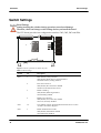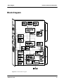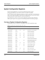
1
SPARC/CPU−56T
Reference Guide
P/N 224548 Revision AA
November 2004
Copyright
The information in this publication is subject to change without notice. Force Computers, GmbH reserves the right to make
changes without notice to this, or any of its products, to improve reliability, performance, or design.a
Force Computers, GmbH shall not be liable for technical or editorial errors or omissions contained herein, nor for indirect,
special, incidental, or consequential damages resulting from the furnishing, performance, or use of this material. This
information is provided "as is" and Force Computers, GmbH expressly disclaims any and all warranties, express, implied,
statutory, or otherwise, including without limitation, any express, statutory, or implied warranty of merchantability, fitness for a
particular purpose, or non−infringement.a
This publication contains information protected by copyright. This publication shall not be reproduced, transmitted, or stored
in a retrieval system, nor its contents used for any purpose, without the prior written consent of Force Computers, GmbH.a
Force Computers, GmbH assumes no responsibility for the use of any circuitry other than circuitry that is part of a product of
Force Computers, GmbH. Force Computers, GmbH does not convey to the purchaser of the product described herein any
license under the patent rights of Force Computers, GmbH nor the rights of others.a
CopyrightE 2004 by Force Computers, GmbH. All rights reserved.
The Force logo is a trademark of Force Computers, GmbH.a
IEEER is a registered trademark of the Institute for Electrical and Electronics Engineers, Inc.a
PICMGR, CompactPCIR, and the CompactPCI logo are registered trademarks and the PICMG logo is a trademark of the PCI
Industrial Computer Manufacturer’s Group.a
AdvancedTCA and ATCA are trademarks of the PCI Computer Manufacturer’s Group.
MS−DOSR, Windows95R, Windows98R, Windows2000R, Windows NTR, Windows Server 2003R and Windows XPR are
registered trademarks and the logos are a trademark of the Microsoft Corporation.
IntelR and PentiumR are registered trademarks and the Intel logo is a trademark of the Intel Corporation.
SPARCR is a registerd trademark, the SPARC logo is a trademark and Ultra SPARCR is a registered trademark of SPARC
International, Inc.
PowerPCR is a registered trademark and the PowerPC logo is a trademark of International Business Machines Corporation.
AltiVecR is a registered trademark and the AltiVec logo is a trademark of Motorola, Inc.
SolarisTMa is a trademark of SUN Microsystems, Inc.
Linux Kernel is a free system kernel developed under the GNU General Public License.
GoAheadR is a registered trademark of GoAhead Software, Inc. and SelfReliantTMa and Self AvailabilityTMa are trademarks of
GoAhead Software, Inc.
LynxOSR and BlueCatR are registered trademarks of LynuxWorks, Inc.
TornadoR, VxWorksR, WindR, WindNavigatorR, Wind River SystemsR, Wind River SystemsR and design, WindViewR,
WinRouterR and XmathR are registered trademarks or service marks of Wind River Systems. Inc.
EnvoyTM, the Tornado logo, Wind RiverTM, and ZincTMa are trademarks or service marks of Wind River Systems, Inc.
SonyR is a registered trademark of Sony Corporation, Japan.
EthernetTMa is a trademark of Xerox Corporation.
Service AvailabilityTMis a trademark of the Service Availability Forum.
PowerQUICCTMis a trademark of Motorola, Inc.
Other product names mentioned herein may be trademarks and/or registered trademarks of their respective companies.
2
SPARC/CPU−56T
World Wide Web: www.fci.com
24−hour access to on−line manuals, driver updates, and application
notes is provided via SMART, our SolutionsPLUS customer support
program that provides current technical and services information.
Headquarters
The Americas
Europe
Asia
Force Computers Inc.
4211 Starboard Drive
Fremont CA 94538
Force Computers GmbH
Lilienthalstr. 15
D−85579 Neubiberg/München
Tel.: +1 (510) 624−5300
Fax: +1 (510) 624−5301
Email: [email protected]
Tel.: +49 (89) 608 14−0
Fax: +49 (89) 609 77 93
Email: support−[email protected]
Force Computers Japan K.K.
Shibadaimon MF Bldg. 4F
Shiba Daimon 2−1−16
Minato−ku, Tokyo 105−0012
Tel.: +81 (03) 3437 3948
Fax: +81 (03) 3437 3968
Email: support−[email protected]
224548 420 000 AA
SPARC/CPU−56T
3
4
SPARC/CPU−56T
Contents
Using this Guide
Other Sources of Information
Safety Notes
Sicherheitshinweise
1
Introduction
Features . . . . . . . . . . . . . . . . . . . . . . . . . . . . . . . . . . . . . . . . . . . . . . . . . . . . . . . . . . . . . . . . 28
Standard Compliances . . . . . . . . . . . . . . . . . . . . . . . . . . . . . . . . . . . . . . . . . . . . . . . . . . . 30
Ordering Information . . . . . . . . . . . . . . . . . . . . . . . . . . . . . . . . . . . . . . . . . . . . . . . . . . . . 31
Product Nomenclature . . . . . . . . . . . . . . . . . . . . . . . . . . . . . . . . . . . . . . . . . . . . . . . . . . . . . . . . . . . . . . . . . . . . 31
Order Numbers . . . . . . . . . . . . . . . . . . . . . . . . . . . . . . . . . . . . . . . . . . . . . . . . . . . . . . . . . . . . . . . . . . . . . . . . . . . 31
2
Installation
Action Plan . . . . . . . . . . . . . . . . . . . . . . . . . . . . . . . . . . . . . . . . . . . . . . . . . . . . . . . . . . . . . 35
Requirements . . . . . . . . . . . . . . . . . . . . . . . . . . . . . . . . . . . . . . . . . . . . . . . . . . . . . . . . . . . 36
Environmental Requirements . . . . . . . . . . . . . . . . . . . . . . . . . . . . . . . . . . . . . . . . . . . . . . . . . . . . . . . . . . . . . . . 36
Power Requirements . . . . . . . . . . . . . . . . . . . . . . . . . . . . . . . . . . . . . . . . . . . . . . . . . . . . . . . . . . . . . . . . . . . . . . 37
Hardware Accessories . . . . . . . . . . . . . . . . . . . . . . . . . . . . . . . . . . . . . . . . . . . . . . . . . . . 38
IOBPs for CPU and I/O Board . . . . . . . . . . . . . . . . . . . . . . . . . . . . . . . . . . . . . . . . . . . . . . . . . . . . . . . . . . . . . . 38
PMC Modules . . . . . . . . . . . . . . . . . . . . . . . . . . . . . . . . . . . . . . . . . . . . . . . . . . . . . . . . . . . . . . . . . . . . . . . . . . . . 39
Installation Procedure . . . . . . . . . . . . . . . . . . . . . . . . . . . . . . . . . . . . . . . . . . . . . . . . . . . . . . . . . . . . . . . . . . 41
Memory Modules . . . . . . . . . . . . . . . . . . . . . . . . . . . . . . . . . . . . . . . . . . . . . . . . . . . . . . . . . . . . . . . . . . . . . . . . . 44
Hard Disk . . . . . . . . . . . . . . . . . . . . . . . . . . . . . . . . . . . . . . . . . . . . . . . . . . . . . . . . . . . . . . . . . . . . . . . . . . . . . . . . 45
SCSI−U160 Cable . . . . . . . . . . . . . . . . . . . . . . . . . . . . . . . . . . . . . . . . . . . . . . . . . . . . . . . . . . . . . . . . . . . . . . . . 45
SPARC/CPU−56T
5
RS−422 Cable . . . . . . . . . . . . . . . . . . . . . . . . . . . . . . . . . . . . . . . . . . . . . . . . . . . . . . . . . . . . . . . . . . . . . . . . . . . 45
PS/2 Splitter Cable . . . . . . . . . . . . . . . . . . . . . . . . . . . . . . . . . . . . . . . . . . . . . . . . . . . . . . . . . . . . . . . . . . . . . . . 45
Switch Settings . . . . . . . . . . . . . . . . . . . . . . . . . . . . . . . . . . . . . . . . . . . . . . . . . . . . . . . . . 46
Board Installation . . . . . . . . . . . . . . . . . . . . . . . . . . . . . . . . . . . . . . . . . . . . . . . . . . . . . . . 48
Backplane Configuration . . . . . . . . . . . . . . . . . . . . . . . . . . . . . . . . . . . . . . . . . . . . . . . . . . . . . . . . . . . . . . . . . . . 48
Installing the CPU Board . . . . . . . . . . . . . . . . . . . . . . . . . . . . . . . . . . . . . . . . . . . . . . . . . . . . . . . . . . . . . . . . . . 49
Removing the CPU Board . . . . . . . . . . . . . . . . . . . . . . . . . . . . . . . . . . . . . . . . . . . . . . . . . . . . . . . . . . . . . . . . . 49
Powering Up . . . . . . . . . . . . . . . . . . . . . . . . . . . . . . . . . . . . . . . . . . . . . . . . . . . . . . . . . . . . . . . . . . . . . . . . . . . . . 50
PLCC PROM and Flash Memory Device . . . . . . . . . . . . . . . . . . . . . . . . . . . . . . . . . . . . . . . . . . . . . . . . . . 50
Installing Solaris . . . . . . . . . . . . . . . . . . . . . . . . . . . . . . . . . . . . . . . . . . . . . . . . . . . . . . . . . . . . . . . . . . . . . . . . . . 51
Solaris Driver Package . . . . . . . . . . . . . . . . . . . . . . . . . . . . . . . . . . . . . . . . . . . . . . . . . . . . . . . . . . . . . . . . . . . .
FRCgei . . . . . . . . . . . . . . . . . . . . . . . . . . . . . . . . . . . . . . . . . . . . . . . . . . . . . . . . . . . . . . . . . . . . . . . . . . . . . . .
FRCvme . . . . . . . . . . . . . . . . . . . . . . . . . . . . . . . . . . . . . . . . . . . . . . . . . . . . . . . . . . . . . . . . . . . . . . . . . . . . .
FRCflash . . . . . . . . . . . . . . . . . . . . . . . . . . . . . . . . . . . . . . . . . . . . . . . . . . . . . . . . . . . . . . . . . . . . . . . . . . . . .
FRCctrl . . . . . . . . . . . . . . . . . . . . . . . . . . . . . . . . . . . . . . . . . . . . . . . . . . . . . . . . . . . . . . . . . . . . . . . . . . . . . . .
FRCplatmod . . . . . . . . . . . . . . . . . . . . . . . . . . . . . . . . . . . . . . . . . . . . . . . . . . . . . . . . . . . . . . . . . . . . . . . . . .
3
52
53
53
54
54
55
Controls, Indicators, and Connectors
Front Panel . . . . . . . . . . . . . . . . . . . . . . . . . . . . . . . . . . . . . . . . . . . . . . . . . . . . . . . . . . . . . 57
LEDs . . . . . . . . . . . . . . . . . . . . . . . . . . . . . . . . . . . . . . . . . . . . . . . . . . . . . . . . . . . . . . . . . . . . . . . . . . . . . . . . . . . . 58
Key . . . . . . . . . . . . . . . . . . . . . . . . . . . . . . . . . . . . . . . . . . . . . . . . . . . . . . . . . . . . . . . . . . . . . . . . . . . . . . . . . . . . . 59
Connectors . . . . . . . . . . . . . . . . . . . . . . . . . . . . . . . . . . . . . . . . . . . . . . . . . . . . . . . . . . . . . . . . . . . . . . . . . . . . . .
Serial I/O . . . . . . . . . . . . . . . . . . . . . . . . . . . . . . . . . . . . . . . . . . . . . . . . . . . . . . . . . . . . . . . . . . . . . . . . . . . . .
Keyboard/Mouse . . . . . . . . . . . . . . . . . . . . . . . . . . . . . . . . . . . . . . . . . . . . . . . . . . . . . . . . . . . . . . . . . . . . . .
Ethernet . . . . . . . . . . . . . . . . . . . . . . . . . . . . . . . . . . . . . . . . . . . . . . . . . . . . . . . . . . . . . . . . . . . . . . . . . . . . . .
SCSI . . . . . . . . . . . . . . . . . . . . . . . . . . . . . . . . . . . . . . . . . . . . . . . . . . . . . . . . . . . . . . . . . . . . . . . . . . . . . . . . .
59
60
60
61
61
On−Board Connectors . . . . . . . . . . . . . . . . . . . . . . . . . . . . . . . . . . . . . . . . . . . . . . . . . . . 63
PMC . . . . . . . . . . . . . . . . . . . . . . . . . . . . . . . . . . . . . . . . . . . . . . . . . . . . . . . . . . . . . . . . . . . . . . . . . . . . . . . . . . . . 63
Memory Module . . . . . . . . . . . . . . . . . . . . . . . . . . . . . . . . . . . . . . . . . . . . . . . . . . . . . . . . . . . . . . . . . . . . . . . . . . 64
IDE . . . . . . . . . . . . . . . . . . . . . . . . . . . . . . . . . . . . . . . . . . . . . . . . . . . . . . . . . . . . . . . . . . . . . . . . . . . . . . . . . . . . . 65
VME . . . . . . . . . . . . . . . . . . . . . . . . . . . . . . . . . . . . . . . . . . . . . . . . . . . . . . . . . . . . . . . . . . . . . . . . . . . . . . . . . . . . 66
CPU Board . . . . . . . . . . . . . . . . . . . . . . . . . . . . . . . . . . . . . . . . . . . . . . . . . . . . . . . . . . . . . . . . . . . . . . . . . . . 66
I/O Board . . . . . . . . . . . . . . . . . . . . . . . . . . . . . . . . . . . . . . . . . . . . . . . . . . . . . . . . . . . . . . . . . . . . . . . . . . . . . 68
6
SPARC/CPU−56T
4
Devices’ Features and Data Paths
Block Diagram . . . . . . . . . . . . . . . . . . . . . . . . . . . . . . . . . . . . . . . . . . . . . . . . . . . . . . . . . . 73
UltraSPARC IIi+ Processor . . . . . . . . . . . . . . . . . . . . . . . . . . . . . . . . . . . . . . . . . . . . . . . 75
Interrupt Controller . . . . . . . . . . . . . . . . . . . . . . . . . . . . . . . . . . . . . . . . . . . . . . . . . . . . . . 76
PCI Bus A . . . . . . . . . . . . . . . . . . . . . . . . . . . . . . . . . . . . . . . . . . . . . . . . . . . . . . . . . . . . . . . 77
Ethernet Controller . . . . . . . . . . . . . . . . . . . . . . . . . . . . . . . . . . . . . . . . . . . . . . . . . . . . . . . . . . . . . . . . . . . . . . . . 77
SCSI Controller . . . . . . . . . . . . . . . . . . . . . . . . . . . . . . . . . . . . . . . . . . . . . . . . . . . . . . . . . . . . . . . . . . . . . . . . . . 77
SENTINEL64 PCI−to−PCI Bridge . . . . . . . . . . . . . . . . . . . . . . . . . . . . . . . . . . . . . . . . . . . . . . . . . . . . . . . . . . . 77
PCI−to−VME Bridge . . . . . . . . . . . . . . . . . . . . . . . . . . . . . . . . . . . . . . . . . . . . . . . . . . . . . . . . . . . . . . . . . . . . . . 77
PCI Bus B . . . . . . . . . . . . . . . . . . . . . . . . . . . . . . . . . . . . . . . . . . . . . . . . . . . . . . . . . . . . . . . 79
Ethernet Controller . . . . . . . . . . . . . . . . . . . . . . . . . . . . . . . . . . . . . . . . . . . . . . . . . . . . . . . . . . . . . . . . . . . . . . . . 79
Southbridge . . . . . . . . . . . . . . . . . . . . . . . . . . . . . . . . . . . . . . . . . . . . . . . . . . . . . . . . . . . . . . . . . . . . . . . . . . . . . . 79
PCIO−2 Controller . . . . . . . . . . . . . . . . . . . . . . . . . . . . . . . . . . . . . . . . . . . . . . . . . . . . . . . . . . . . . . . . . . . . . . . .
EBus Interface . . . . . . . . . . . . . . . . . . . . . . . . . . . . . . . . . . . . . . . . . . . . . . . . . . . . . . . . . . . . . . . . . . . . . . . .
Media Independent Interface . . . . . . . . . . . . . . . . . . . . . . . . . . . . . . . . . . . . . . . . . . . . . . . . . . . . . . . . . . . .
USB Interfaces . . . . . . . . . . . . . . . . . . . . . . . . . . . . . . . . . . . . . . . . . . . . . . . . . . . . . . . . . . . . . . . . . . . . . . . .
79
79
80
80
EBus . . . . . . . . . . . . . . . . . . . . . . . . . . . . . . . . . . . . . . . . . . . . . . . . . . . . . . . . . . . . . . . . . . . 81
FPGA . . . . . . . . . . . . . . . . . . . . . . . . . . . . . . . . . . . . . . . . . . . . . . . . . . . . . . . . . . . . . . . . . . . . . . . . . . . . . . . . . . .
Watchdog . . . . . . . . . . . . . . . . . . . . . . . . . . . . . . . . . . . . . . . . . . . . . . . . . . . . . . . . . . . . . . . . . . . . . . . . . . . .
Timer . . . . . . . . . . . . . . . . . . . . . . . . . . . . . . . . . . . . . . . . . . . . . . . . . . . . . . . . . . . . . . . . . . . . . . . . . . . . . . . .
Temperature Sensor Control . . . . . . . . . . . . . . . . . . . . . . . . . . . . . . . . . . . . . . . . . . . . . . . . . . . . . . . . . . . .
Local I2C Interface . . . . . . . . . . . . . . . . . . . . . . . . . . . . . . . . . . . . . . . . . . . . . . . . . . . . . . . . . . . . . . . . . . . . .
Ethernet Interface 1/3 Switching . . . . . . . . . . . . . . . . . . . . . . . . . . . . . . . . . . . . . . . . . . . . . . . . . . . . . . . . .
LED and Switch Control . . . . . . . . . . . . . . . . . . . . . . . . . . . . . . . . . . . . . . . . . . . . . . . . . . . . . . . . . . . . . . . .
Reset Control . . . . . . . . . . . . . . . . . . . . . . . . . . . . . . . . . . . . . . . . . . . . . . . . . . . . . . . . . . . . . . . . . . . . . . . . .
81
81
82
82
82
83
83
83
PLCC PROM and Flash Memory Device . . . . . . . . . . . . . . . . . . . . . . . . . . . . . . . . . . . . . . . . . . . . . . . . . . . . . 84
Real−Time Clock and NVRAM . . . . . . . . . . . . . . . . . . . . . . . . . . . . . . . . . . . . . . . . . . . . . . . . . . . . . . . . . . . . . . 84
Serial Controller . . . . . . . . . . . . . . . . . . . . . . . . . . . . . . . . . . . . . . . . . . . . . . . . . . . . . . . . . . . . . . . . . . . . . . . . . . 84
PCI Bus C . . . . . . . . . . . . . . . . . . . . . . . . . . . . . . . . . . . . . . . . . . . . . . . . . . . . . . . . . . . . . . . 86
5
OpenBoot Firmware
Introduction . . . . . . . . . . . . . . . . . . . . . . . . . . . . . . . . . . . . . . . . . . . . . . . . . . . . . . . . . . . . . 88
CORE . . . . . . . . . . . . . . . . . . . . . . . . . . . . . . . . . . . . . . . . . . . . . . . . . . . . . . . . . . . . . . . . . . . . . . . . . . . . . . . . . . . 88
SPARC/CPU−56T
7
CORE Workflow . . . . . . . . . . . . . . . . . . . . . . . . . . . . . . . . . . . . . . . . . . . . . . . . . . . . . . . . . . . . . . . . . . . . . . . 89
CORE Commands . . . . . . . . . . . . . . . . . . . . . . . . . . . . . . . . . . . . . . . . . . . . . . . . . . . . . . . . . . . . . . . . . . . . . 90
POST . . . . . . . . . . . . . . . . . . . . . . . . . . . . . . . . . . . . . . . . . . . . . . . . . . . . . . . . . . . . . . . . . . . . . . . . . . . . . . . . . . . 90
OpenBoot . . . . . . . . . . . . . . . . . . . . . . . . . . . . . . . . . . . . . . . . . . . . . . . . . . . . . . . . . . . . . . . . . . . . . . . . . . . . . . . 90
Optional Boot Parameters . . . . . . . . . . . . . . . . . . . . . . . . . . . . . . . . . . . . . . . . . . . . . . . . . . . . . . . . . . . . . . 91
Boot Devices . . . . . . . . . . . . . . . . . . . . . . . . . . . . . . . . . . . . . . . . . . . . . . . . . . . . . . . . . . . . . . . . . . . . . . . . . . 91
OBDIAG . . . . . . . . . . . . . . . . . . . . . . . . . . . . . . . . . . . . . . . . . . . . . . . . . . . . . . . . . . . . . . . . . . . . . . . . . . . . . . . . .
Executing OBDIAG . . . . . . . . . . . . . . . . . . . . . . . . . . . . . . . . . . . . . . . . . . . . . . . . . . . . . . . . . . . . . . . . . . . .
Terminating OBDIAG . . . . . . . . . . . . . . . . . . . . . . . . . . . . . . . . . . . . . . . . . . . . . . . . . . . . . . . . . . . . . . . . . . .
OBDIAG Commands . . . . . . . . . . . . . . . . . . . . . . . . . . . . . . . . . . . . . . . . . . . . . . . . . . . . . . . . . . . . . . . . . . .
94
94
95
95
VxWorks Support . . . . . . . . . . . . . . . . . . . . . . . . . . . . . . . . . . . . . . . . . . . . . . . . . . . . . . . . . . . . . . . . . . . . . . . . . 96
NVRAM Boot Parameters . . . . . . . . . . . . . . . . . . . . . . . . . . . . . . . . . . . . . . . . . . . . . . . . 97
Diagnostics . . . . . . . . . . . . . . . . . . . . . . . . . . . . . . . . . . . . . . . . . . . . . . . . . . . . . . . . . . . . . 98
SCSI Bus . . . . . . . . . . . . . . . . . . . . . . . . . . . . . . . . . . . . . . . . . . . . . . . . . . . . . . . . . . . . . . . . . . . . . . . . . . . . . . . . 98
All SCSI Buses . . . . . . . . . . . . . . . . . . . . . . . . . . . . . . . . . . . . . . . . . . . . . . . . . . . . . . . . . . . . . . . . . . . . . . . . . . . 98
Single Device . . . . . . . . . . . . . . . . . . . . . . . . . . . . . . . . . . . . . . . . . . . . . . . . . . . . . . . . . . . . . . . . . . . . . . . . . . . . 99
Group of Devices . . . . . . . . . . . . . . . . . . . . . . . . . . . . . . . . . . . . . . . . . . . . . . . . . . . . . . . . . . . . . . . . . . . . . . . . . 99
Clock . . . . . . . . . . . . . . . . . . . . . . . . . . . . . . . . . . . . . . . . . . . . . . . . . . . . . . . . . . . . . . . . . . . . . . . . . . . . . . . . . . . 99
Network . . . . . . . . . . . . . . . . . . . . . . . . . . . . . . . . . . . . . . . . . . . . . . . . . . . . . . . . . . . . . . . . . . . . . . . . . . . . . . . . 100
IDE Devices . . . . . . . . . . . . . . . . . . . . . . . . . . . . . . . . . . . . . . . . . . . . . . . . . . . . . . . . . . . . . . . . . . . . . . . . . . . . 100
Displaying System Information . . . . . . . . . . . . . . . . . . . . . . . . . . . . . . . . . . . . . . . . . . 101
Ethernet Address and Host ID . . . . . . . . . . . . . . . . . . . . . . . . . . . . . . . . . . . . . . . . . . . . . . . . . . . . . . . . . . . . . 101
ID PROM . . . . . . . . . . . . . . . . . . . . . . . . . . . . . . . . . . . . . . . . . . . . . . . . . . . . . . . . . . . . . . . . . . . . . . . . . . . . . . . 101
Resetting the System . . . . . . . . . . . . . . . . . . . . . . . . . . . . . . . . . . . . . . . . . . . . . . . . . . . 103
Activating OpenBoot Help . . . . . . . . . . . . . . . . . . . . . . . . . . . . . . . . . . . . . . . . . . . . . . . 104
6
Maps and Registers
Interrupt Map . . . . . . . . . . . . . . . . . . . . . . . . . . . . . . . . . . . . . . . . . . . . . . . . . . . . . . . . . . . 108
Physical Memory Map . . . . . . . . . . . . . . . . . . . . . . . . . . . . . . . . . . . . . . . . . . . . . . . . . . 110
UltraSPARC−IIi+ Physical Address Memory Map . . . . . . . . . . . . . . . . . . . . . . . . . . . . . . . . . . . . . . . . . . . . 110
Memory Address Map . . . . . . . . . . . . . . . . . . . . . . . . . . . . . . . . . . . . . . . . . . . . . . . . . . . . . . . . . . . . . . . . . . . . 110
8
SPARC/CPU−56T
UltraSPARC−IIi+ Internal CSR Space . . . . . . . . . . . . . . . . . . . . . . . . . . . . . . . . . . . . . . . . . . . . . . . . . . . . . . 111
PCI Bus Address Map . . . . . . . . . . . . . . . . . . . . . . . . . . . . . . . . . . . . . . . . . . . . . . . . . . . . . . . . . . . . . . . . . . . . 111
PCIO−2 Address Map . . . . . . . . . . . . . . . . . . . . . . . . . . . . . . . . . . . . . . . . . . . . . . . . . . . . . . . . . . . . . . . . . . . . 112
System Configuration Registers . . . . . . . . . . . . . . . . . . . . . . . . . . . . . . . . . . . . . . . . . 114
Overview of System Configuration Registers . . . . . . . . . . . . . . . . . . . . . . . . . . . . . . . . . . . . . . . . . . . . . . . . 114
Miscellaneous Control Register . . . . . . . . . . . . . . . . . . . . . . . . . . . . . . . . . . . . . . . . . . . . . . . . . . . . . . . . . . . . 115
User LED Control Registers . . . . . . . . . . . . . . . . . . . . . . . . . . . . . . . . . . . . . . . . . . . . . . . . . . . . . . . . . . . . . . .
LED Control Register 1 . . . . . . . . . . . . . . . . . . . . . . . . . . . . . . . . . . . . . . . . . . . . . . . . . . . . . . . . . . . . . . . .
LED Control Register 2 . . . . . . . . . . . . . . . . . . . . . . . . . . . . . . . . . . . . . . . . . . . . . . . . . . . . . . . . . . . . . . . .
LED Control Register 3 . . . . . . . . . . . . . . . . . . . . . . . . . . . . . . . . . . . . . . . . . . . . . . . . . . . . . . . . . . . . . . . .
LED Control Register 4 . . . . . . . . . . . . . . . . . . . . . . . . . . . . . . . . . . . . . . . . . . . . . . . . . . . . . . . . . . . . . . . .
117
117
118
118
119
External Failure Status Register . . . . . . . . . . . . . . . . . . . . . . . . . . . . . . . . . . . . . . . . . . . . . . . . . . . . . . . . . . . 120
Watchdog Timer Registers . . . . . . . . . . . . . . . . . . . . . . . . . . . . . . . . . . . . . . . . . . . . . . . . . . . . . . . . . . . . . . . .
Watchdog Timer Control Register . . . . . . . . . . . . . . . . . . . . . . . . . . . . . . . . . . . . . . . . . . . . . . . . . . . . . . .
Watchdog Timer Trigger Register . . . . . . . . . . . . . . . . . . . . . . . . . . . . . . . . . . . . . . . . . . . . . . . . . . . . . . .
Watchdog Timer Status Register . . . . . . . . . . . . . . . . . . . . . . . . . . . . . . . . . . . . . . . . . . . . . . . . . . . . . . . .
121
121
122
123
Timer Registers . . . . . . . . . . . . . . . . . . . . . . . . . . . . . . . . . . . . . . . . . . . . . . . . . . . . . . . . . . . . . . . . . . . . . . . . .
Timer Control Register . . . . . . . . . . . . . . . . . . . . . . . . . . . . . . . . . . . . . . . . . . . . . . . . . . . . . . . . . . . . . . . .
Timer Clear Control Register . . . . . . . . . . . . . . . . . . . . . . . . . . . . . . . . . . . . . . . . . . . . . . . . . . . . . . . . . . .
Timer Status Register . . . . . . . . . . . . . . . . . . . . . . . . . . . . . . . . . . . . . . . . . . . . . . . . . . . . . . . . . . . . . . . . .
Timer Initial Control Registers . . . . . . . . . . . . . . . . . . . . . . . . . . . . . . . . . . . . . . . . . . . . . . . . . . . . . . . . . .
Timer Counter Status Register . . . . . . . . . . . . . . . . . . . . . . . . . . . . . . . . . . . . . . . . . . . . . . . . . . . . . . . . .
123
123
124
124
125
126
Interrupt Registers . . . . . . . . . . . . . . . . . . . . . . . . . . . . . . . . . . . . . . . . . . . . . . . . . . . . . . . . . . . . . . . . . . . . . . . 127
Interrupt Enable Control Register . . . . . . . . . . . . . . . . . . . . . . . . . . . . . . . . . . . . . . . . . . . . . . . . . . . . . . . 127
Interrupt Pending Status Register . . . . . . . . . . . . . . . . . . . . . . . . . . . . . . . . . . . . . . . . . . . . . . . . . . . . . . . 128
Reset Register . . . . . . . . . . . . . . . . . . . . . . . . . . . . . . . . . . . . . . . . . . . . . . . . . . . . . . . . . . . . . . . . . . . . . . . . . . 129
Board Status Registers . . . . . . . . . . . . . . . . . . . . . . . . . . . . . . . . . . . . . . . . . . . . . . . . . . . . . . . . . . . . . . . . . . .
Switch 1 and 2 Status Register . . . . . . . . . . . . . . . . . . . . . . . . . . . . . . . . . . . . . . . . . . . . . . . . . . . . . . . . .
Switch 3 and 4 Status Register . . . . . . . . . . . . . . . . . . . . . . . . . . . . . . . . . . . . . . . . . . . . . . . . . . . . . . . . .
Board Configuration Status Register 1 . . . . . . . . . . . . . . . . . . . . . . . . . . . . . . . . . . . . . . . . . . . . . . . . . . .
Board Configuration Status Register 2 . . . . . . . . . . . . . . . . . . . . . . . . . . . . . . . . . . . . . . . . . . . . . . . . . . .
130
130
131
132
133
Hardware Revision Register . . . . . . . . . . . . . . . . . . . . . . . . . . . . . . . . . . . . . . . . . . . . . . . . . . . . . . . . . . . . . . 133
I2C Registers . . . . . . . . . . . . . . . . . . . . . . . . . . . . . . . . . . . . . . . . . . . . . . . . . . . . . . . . . . . . . . . . . . . . . . . . . . . 134
AppendixA Troubleshooting
AppendixB Battery Exchange
Index
SPARC/CPU−56T
9
Product Error Report
10
SPARC/CPU−56T
Tables
Introduction
Tablei1aaaaaaaStandard Compliances . . . . . . . . . . . . . . . . . . . . . . . . . . . . . . . . . . . . . . . . . . . . . . . . . . . . . . . . . . . .
Tablei2aaaaaaaProduct Nomenclature . . . . . . . . . . . . . . . . . . . . . . . . . . . . . . . . . . . . . . . . . . . . . . . . . . . . . . . . . . . .
Tablei3aaaaaaaBoard Ordering Information . . . . . . . . . . . . . . . . . . . . . . . . . . . . . . . . . . . . . . . . . . . . . . . . . . . . . . . .
Tablei4aaaaaaaBoard Accessories Ordering Information . . . . . . . . . . . . . . . . . . . . . . . . . . . . . . . . . . . . . . . . . . . .
30
31
31
31
Installation
Tablei5aaaaaaaEnvironmental Requirements . . . . . . . . . . . . . . . . . . . . . . . . . . . . . . . . . . . . . . . . . . . . . . . . . . . . . .
Tablei6aaaaaaaPower Requirements . . . . . . . . . . . . . . . . . . . . . . . . . . . . . . . . . . . . . . . . . . . . . . . . . . . . . . . . . . . . .
Tablei7aaaaaaaSwitch Settings . . . . . . . . . . . . . . . . . . . . . . . . . . . . . . . . . . . . . . . . . . . . . . . . . . . . . . . . . . . . . . . . . .
Tablei8aaaaaaaSolaris Patches . . . . . . . . . . . . . . . . . . . . . . . . . . . . . . . . . . . . . . . . . . . . . . . . . . . . . . . . . . . . . . . . . .
Tablei9aaaaaaaDevices and Their Appropriate Drivers . . . . . . . . . . . . . . . . . . . . . . . . . . . . . . . . . . . . . . . . . . . . . .
Tablei10aaaaaaFlash Segmentation and Write Protection . . . . . . . . . . . . . . . . . . . . . . . . . . . . . . . . . . . . . . . . . . .
36
37
46
52
52
54
Controls, Indicators, and Connectors
Tablei11aaaaaaDescription of Front Panel LEDs . . . . . . . . . . . . . . . . . . . . . . . . . . . . . . . . . . . . . . . . . . . . . . . . . . . 58
Devices’ Features and Data Paths
Tablei12aaaaaaReset Sources . . . . . . . . . . . . . . . . . . . . . . . . . . . . . . . . . . . . . . . . . . . . . . . . . . . . . . . . . . . . . . . . . . . 83
OpenBoot Firmware
Tablei13aaaaaaBoot Parameters . . . . . . . . . . . . . . . . . . . . . . . . . . . . . . . . . . . . . . . . . . . . . . . . . . . . . . . . . . . . . . . . . 91
Tablei14aaaaaaOpenBoot Aliases for SCSI Devices . . . . . . . . . . . . . . . . . . . . . . . . . . . . . . . . . . . . . . . . . . . . . . . . 91
Tablei15aaaaaaOpenBoot Aliases for Miscellaneous Devices . . . . . . . . . . . . . . . . . . . . . . . . . . . . . . . . . . . . . . . . 93
Tablei16aaaaaaOBDIAG Commands . . . . . . . . . . . . . . . . . . . . . . . . . . . . . . . . . . . . . . . . . . . . . . . . . . . . . . . . . . . . . 95
Tablei17aaaaaaOpenBoot Configuration Parameters . . . . . . . . . . . . . . . . . . . . . . . . . . . . . . . . . . . . . . . . . . . . . . . 97
Tablei18aaaaaaDiagnostic Routines . . . . . . . . . . . . . . . . . . . . . . . . . . . . . . . . . . . . . . . . . . . . . . . . . . . . . . . . . . . . . . 98
Tablei19aaaaaaCommands to Display System Information . . . . . . . . . . . . . . . . . . . . . . . . . . . . . . . . . . . . . . . . . 102
Maps and Registers
Tablei20aaaaaaUltraSPARC−IIi+ Main Address Map . . . . . . . . . . . . . . . . . . . . . . . . . . . . . . . . . . . . . . . . . . . . . . .
Tablei21aaaaaaMain Memory Address Map . . . . . . . . . . . . . . . . . . . . . . . . . . . . . . . . . . . . . . . . . . . . . . . . . . . . . .
Tablei22aaaaaaUltraSPARC−IIi+ Internal CSR Space . . . . . . . . . . . . . . . . . . . . . . . . . . . . . . . . . . . . . . . . . . . . . .
Tablei23aaaaaaPCI Bus Address Map . . . . . . . . . . . . . . . . . . . . . . . . . . . . . . . . . . . . . . . . . . . . . . . . . . . . . . . . . . .
Tablei24aaaaaaPCIO−2 Address Map . . . . . . . . . . . . . . . . . . . . . . . . . . . . . . . . . . . . . . . . . . . . . . . . . . . . . . . . . . .
Tablei25aaaaaaCPU Board System Configuration Register Address Map . . . . . . . . . . . . . . . . . . . . . . . . . . . . .
Tablei26aaaaaaMiscellaneous Control Register . . . . . . . . . . . . . . . . . . . . . . . . . . . . . . . . . . . . . . . . . . . . . . . . . . .
Tablei27aaaaaaLED Control Register 1 . . . . . . . . . . . . . . . . . . . . . . . . . . . . . . . . . . . . . . . . . . . . . . . . . . . . . . . . . .
Tablei28aaaaaaLED Control Register 2 . . . . . . . . . . . . . . . . . . . . . . . . . . . . . . . . . . . . . . . . . . . . . . . . . . . . . . . . . .
SPARC/CPU−56T
110
110
111
112
112
114
116
117
118
11
Tablei29aaaaaaLED Control Register 3 . . . . . . . . . . . . . . . . . . . . . . . . . . . . . . . . . . . . . . . . . . . . . . . . . . . . . . . . . .
Tablei30aaaaaaLED Control Register 4 . . . . . . . . . . . . . . . . . . . . . . . . . . . . . . . . . . . . . . . . . . . . . . . . . . . . . . . . . .
Tablei31aaaaaaExternal Failure Register . . . . . . . . . . . . . . . . . . . . . . . . . . . . . . . . . . . . . . . . . . . . . . . . . . . . . . . . .
Tablei32aaaaaaWatchdog Timer Control Register . . . . . . . . . . . . . . . . . . . . . . . . . . . . . . . . . . . . . . . . . . . . . . . . .
Tablei33aaaaaaWatchdog Timer Trigger Register . . . . . . . . . . . . . . . . . . . . . . . . . . . . . . . . . . . . . . . . . . . . . . . . .
Tablei34aaaaaaWatchdog Timer Status Register . . . . . . . . . . . . . . . . . . . . . . . . . . . . . . . . . . . . . . . . . . . . . . . . . .
Tablei35aaaaaaTimer Control Register . . . . . . . . . . . . . . . . . . . . . . . . . . . . . . . . . . . . . . . . . . . . . . . . . . . . . . . . . . .
Tablei36aaaaaaTimer Clear Control Register . . . . . . . . . . . . . . . . . . . . . . . . . . . . . . . . . . . . . . . . . . . . . . . . . . . . .
Tablei37aaaaaaTimer Status Register . . . . . . . . . . . . . . . . . . . . . . . . . . . . . . . . . . . . . . . . . . . . . . . . . . . . . . . . . . . .
Tablei38aaaaaaTimer Initial Control Registers . . . . . . . . . . . . . . . . . . . . . . . . . . . . . . . . . . . . . . . . . . . . . . . . . . . . .
Tablei39aaaaaaTimer Counter Status Register . . . . . . . . . . . . . . . . . . . . . . . . . . . . . . . . . . . . . . . . . . . . . . . . . . . .
Tablei40aaaaaaInterrupt Enable Control Register . . . . . . . . . . . . . . . . . . . . . . . . . . . . . . . . . . . . . . . . . . . . . . . . . .
Tablei41aaaaaaInterrupt Pending Status Register . . . . . . . . . . . . . . . . . . . . . . . . . . . . . . . . . . . . . . . . . . . . . . . . .
Tablei42aaaaaaReset Status Register . . . . . . . . . . . . . . . . . . . . . . . . . . . . . . . . . . . . . . . . . . . . . . . . . . . . . . . . . . .
Tablei43aaaaaaSwitch 1 and 2 StatusRegister . . . . . . . . . . . . . . . . . . . . . . . . . . . . . . . . . . . . . . . . . . . . . . . . . . . .
Tablei44aaaaaaSwitch 3 and 4 Status Register . . . . . . . . . . . . . . . . . . . . . . . . . . . . . . . . . . . . . . . . . . . . . . . . . . .
Tablei45aaaaaaBoard Configuration Status Register 1 . . . . . . . . . . . . . . . . . . . . . . . . . . . . . . . . . . . . . . . . . . . . .
Tablei46aaaaaaBoard Configuration Status Register 2 . . . . . . . . . . . . . . . . . . . . . . . . . . . . . . . . . . . . . . . . . . . . .
Tablei47aaaaaaHardware Revision Register . . . . . . . . . . . . . . . . . . . . . . . . . . . . . . . . . . . . . . . . . . . . . . . . . . . . . .
Tablei48aaaaaaI2C 1 Register . . . . . . . . . . . . . . . . . . . . . . . . . . . . . . . . . . . . . . . . . . . . . . . . . . . . . . . . . . . . . . . . . .
Tablei49aaaaaaI2C 2 Register . . . . . . . . . . . . . . . . . . . . . . . . . . . . . . . . . . . . . . . . . . . . . . . . . . . . . . . . . . . . . . . . . .
12
119
120
120
122
122
123
124
124
125
126
127
128
128
129
130
131
132
133
134
134
135
SPARC/CPU−56T
Figures
Introduction
Figurei1aaaaaaaFunction Blocks . . . . . . . . . . . . . . . . . . . . . . . . . . . . . . . . . . . . . . . . . . . . . . . . . . . . . . . . . . . . . . . . . 29
Installation
Figurei2aaaaaaaLocation of PMC Voltage Keys . . . . . . . . . . . . . . . . . . . . . . . . . . . . . . . . . . . . . . . . . . . . . . . . . . . . 40
Figurei3aaaaaaaLocation of Switches on Board’s Top Side . . . . . . . . . . . . . . . . . . . . . . . . . . . . . . . . . . . . . . . . . . 46
Controls, Indicators, and Connectors
Figurei4aaaaaaaCPU Board’s Front Panel . . . . . . . . . . . . . . . . . . . . . . . . . . . . . . . . . . . . . . . . . . . . . . . . . . . . . . . . .
Figurei5aaaaaaaSerial A Connector Pinout . . . . . . . . . . . . . . . . . . . . . . . . . . . . . . . . . . . . . . . . . . . . . . . . . . . . . . . .
Figurei6aaaaaaaSerial B Connector Pinout . . . . . . . . . . . . . . . . . . . . . . . . . . . . . . . . . . . . . . . . . . . . . . . . . . . . . . . .
Figurei7aaaaaaaSUN−Type Keyboard/Mouse Connector Pinout . . . . . . . . . . . . . . . . . . . . . . . . . . . . . . . . . . . . . .
Figurei8aaaaaaaPS/2 Keyboard Connector Pinout . . . . . . . . . . . . . . . . . . . . . . . . . . . . . . . . . . . . . . . . . . . . . . . . .
Figurei9aaaaaaaPS/2 Mouse Connector Pinout . . . . . . . . . . . . . . . . . . . . . . . . . . . . . . . . . . . . . . . . . . . . . . . . . . . .
Figurei10aaaaaaEthernet 1 Connector Pinout . . . . . . . . . . . . . . . . . . . . . . . . . . . . . . . . . . . . . . . . . . . . . . . . . . . . . .
Figurei11aaaaaaEthernet 2 Connector Pinout . . . . . . . . . . . . . . . . . . . . . . . . . . . . . . . . . . . . . . . . . . . . . . . . . . . . . .
Figurei12aaaaaaSCSI 1/2 Connector Pinouts . . . . . . . . . . . . . . . . . . . . . . . . . . . . . . . . . . . . . . . . . . . . . . . . . . . . . .
Figurei13aaaaaaLocation of PMC Connectors . . . . . . . . . . . . . . . . . . . . . . . . . . . . . . . . . . . . . . . . . . . . . . . . . . . . .
Figurei14aaaaaaPMC I/O Connector Pn24 Pinout . . . . . . . . . . . . . . . . . . . . . . . . . . . . . . . . . . . . . . . . . . . . . . . . . .
Figurei15aaaaaaLocation of Memory Module Connectors . . . . . . . . . . . . . . . . . . . . . . . . . . . . . . . . . . . . . . . . . . .
Figurei16aaaaaaIDE Connector Pinout . . . . . . . . . . . . . . . . . . . . . . . . . . . . . . . . . . . . . . . . . . . . . . . . . . . . . . . . . . . .
Figurei17aaaaaaLocation of VME Connectors . . . . . . . . . . . . . . . . . . . . . . . . . . . . . . . . . . . . . . . . . . . . . . . . . . . . .
Figurei18aaaaaaCPU Board P2 VMEbus Connector Pinout Rows Z − B . . . . . . . . . . . . . . . . . . . . . . . . . . . . . . .
Figurei19aaaaaaCPU Board P2 VMEbus Connector Pinout Rows C + D . . . . . . . . . . . . . . . . . . . . . . . . . . . . . .
Figurei20aaaaaaI/O Board P2 VMEbus Connector Pinout Rows Z – B . . . . . . . . . . . . . . . . . . . . . . . . . . . . . . . .
Figurei21aaaaaaI/O Board P2 VMEbus Connector Pinout Rows C + D . . . . . . . . . . . . . . . . . . . . . . . . . . . . . . . .
57
60
60
60
60
61
61
61
62
63
64
65
66
66
67
68
69
70
Devices’ Features and Data Paths
Figurei22aaaaaaCPU Board Block Diagram . . . . . . . . . . . . . . . . . . . . . . . . . . . . . . . . . . . . . . . . . . . . . . . . . . . . . . . 73
Figurei23aaaaaaI/O Board Block Diagram . . . . . . . . . . . . . . . . . . . . . . . . . . . . . . . . . . . . . . . . . . . . . . . . . . . . . . . . . 74
OpenBoot Firmware
Figurei24aaaaaaOpenBoot CORE Overview . . . . . . . . . . . . . . . . . . . . . . . . . . . . . . . . . . . . . . . . . . . . . . . . . . . . . . . 88
Figurei25aaaaaa48−bit (6−byte) Ethernet Address . . . . . . . . . . . . . . . . . . . . . . . . . . . . . . . . . . . . . . . . . . . . . . . . . 101
Figurei26aaaaaa32−bit (4−byte) Host ID . . . . . . . . . . . . . . . . . . . . . . . . . . . . . . . . . . . . . . . . . . . . . . . . . . . . . . . . . 101
SPARC/CPU−56T
13
Using this Guide
This Reference Guide is intended for users qualified in electronics or electrical
engineering. Users must have a working understanding of Peripheral Component
Interconnect (PCI), VMEbus, and telecommunications.
Conventions
Notation
Description
57
All numbers are decimal numbers except when used with the
notations described below.
00000000 16
or 0x00000000
Typical notation for hexadecimal numbers (digits 0 through F),
e.g. used for addresses and offsets
00002
or 0b0000
Same for binary numbers (digits are 0 and 1)
x
Generic use of a letter
n
Generic use of numbers
0.75
Decimal number
Bold
Used to emphasize a word
Courier
Used for on−screen output
Courier+Bold
Used to characterize user input
Italics
For references, table, and figure descriptions
File > Exit
Notation for selecting a submenu
<text>
Notation for variables and keys
[text]
Notation for buttons and optional parameters
...
Repeated item (example: A1, A2, A3, ..., A12)
.
.
.
Omission of information from example/command that is not
necessary at the time being
..
Ranges, e.g.: 0..4 means one of the integers 0, 1, 2, 3, and 4
(used in register description tables)
|
Logical OR
No danger encountered. Pay attention to important
information
14
SPARC/CPU−56T
Notation
Description
Possibly dangerous situation: slight injuries to people or
damage to objects possible
Dangerous situation: injuries to people or severe damage to
objects possible
Start of a p
procedure
End of a p
procedure
Abbreviations
Abbreviation
Description
B
B
BGA
BIB
BMC
Ball Grid Array
Board Information Block
Base Board Management Controller
C
C
CAS
CSR
Column Address Select
Control Status Register
D
D
DMA
DRAM
Direct Memory Access
Dynamic Random Access Memory
E
E
ECC
EEPROM
EPROM
ESD
Error−Correction Code
Electrically Erasable Programmable Read−Only Memory
Erasable Programmable Read Only Memory
Electrostatic Sensitive Device
SPARC/CPU−56T
15
16
Abbreviation
Description
F
F
FAE
FIFO
Field Application Engineers
First In First Out
FPGA
Field−Programmable Gate Array
I
I
IBMU
ICMB
Intelligent Board Management Unit
Intelligent Chassis Management Bus
ICT
In−Circuit Test
IDE
Integrated Drive Electronics
IEC
International Electric Code
IOBP
Input Output Back Panel
IOM
I/O Memory Management Unit
IPMB
Intelligent Platform Management Bus
IPMI
Intelligent Platform Management Interface
ISO
International Organization for Standardization
J
J
JTAG
Joint Test Access Group
L
L
LCA
LDO
Load Controller Assembly
Local Data Output
LED
Light Emitting Diode
LVD
Low Voltage Differential
LVTTL
Low Voltage Transistor Transistor Logic
M
M
MAC
MCU
Media Access Control Layer
Memory Control Unit
MII
Media Independent Interface
N
N
NEBS
NMI
Network Equipment Building Standards
Nonmaskable Interrupt
NVRAM
Nonvolatile Random Access Memory
O
O
OBDIAG
OpenBoot Diagnostics
P
P
PBM
PCB
PCI Bus Module
Printed Circuit Board
PCI
Peripheral Component Interconnect
SPARC/CPU−56T
Abbreviation
PCIO
PHY
PIE
PLCC
PLL
PMC
POST
PROM
Description
Peripheral Component Interconnect Input/Output
Physical Layer
PCI Interrupt Engine
Plastic Leadless Chip Carrier
Phase−Locked Loop
PCI Mezzanine Card
Power−On Self−Test
Programmable Read Only Memory
R
R
RIC
ROM
RTB
RTC
RTOS
Reset/Interrupt/Clock Controller
Read Only Memory
Rear Transition Board
Real−Time Clock
Real Time Operating System
S
S
SDRAM
SELV
SPD
SRAM
STP
Synchronous DRAM
Safety Extra Low Voltages
Serial Presence Detect
Static Random Access Memory
Shielded Twisted Pair
T
T
TPE
Twisted Pair Ethernet
U
U
UART
UIC
USB
UTP
Universal Asynchronous Receiver−Transmitter
UPA Interrupt Connector
Universal Serial Bus
Unshielded Twisted Pair
V
V
VME
Versa Module Eurocard
Revision History
Order No.
Rev.
Date
Description
220306
AA
May 2003
Preliminary
Manual
220306
AB
September 2003
Final release
version
SPARC/CPU−56T
17
18
Order No.
Rev.
Date
Description
223146
AA
April 2004
Corrected number
of SUN patch for
audio support.
Now it reads
109896−17; added
note to abort/reset
key description;
corrected feature
list of FRctrl
Solaris driver
224548
AA
November 2004
Corrected typical
and maximum
power
consumption
values for 5V.a
SPARC/CPU−56T
Other Sources of Information
For further information refer to:
Company
www.
Document
ALI Corporation
ali.com.tw
ALI M1535D+ Southbridge documentation
Force Computers forcecomputers.com
SPARC/IOBP−CPU−56 Installation Guide
aa
SPARC/IOBP−IO−56 Installation Guide
SPARC/MEM−550 Installation Guidea
ACC/CABLE/SCSI−U160 Installation Guide
ACC/CABLE/RS422 Installation Guide
IEEE Standards
Department
ieee.com
IEEE P1386 Standard Mechanics for a Common
Mezzanine Card Family: CMC
Intel
intel.com
Intel 82540 Ethernet controller specifications
aa
aa
Intel LXT971 PHY device specifications
LSI Logic
lsilogic.com
53C1010 SCSI controller specifications
Maxim
maxim−ic.com
MAX1617 temperature sensor specifications
STMicroelectroni
cs
st.com
M48T35AV RTC/NVRAM specifications
National
Semiconductor
national.com
PC87307/PC97307 Plug and Play Compatible
Super I/O, Preliminary Specification, March
1998
PCI Special
Interest Group
pcisig.com
PCI Local Bus Specification Rev2.1
PICMGPCI
Special Interest
Group
picmg.org
pcisig.com
PCI Local Bus Specification Rev2.2
SUN
sun.com
UltraSPARCIIi+ Processor specifications
aa
aa
SUN SME2300 PCIO−2 controller
documentation
Tundra
tundra.com
Universe II documentation
VITA
vita.com
VME64 Standard ANSI/VITA 1−1994
aa
aa
VME64 Extensions Draft Standard, Draft 1.8, Jun
13, 1997
Xilinx
xilinx.com
Spartan XC520XL FPGA specifications
SPARC/CPU−56T
19
Safety Notes
The text in this chapter is a translation of the Sicherheitshinweise" chapter
This section provides safety precautions to follow when installing, operating, and
maintaining the board.
We intend to provide all necessary information to install and handle the board in this
Installation Guide. However, as the product is complex and its usage manifold, we do not
guarantee that the given information is complete. If you need additional information, ask
your Force Computers representative.
The board has been designed to meet the standard industrial safety requirements. It
must not be used except in its specific area of office telecommunication industry and
industrial control.
Only personnel trained by Force Computers or persons qualified in electronics or
electrical engineering are authorized to install, remove or maintain the board. The
information given in this manual is meant to complete the knowledge of a specialist
and must not be taken as replacement for qualified personnel.
EMC
The board has been tested in a Standard Force Computers system and found to comply
with the limits for a Class A digital device in this system, pursuant to part 15 of the
FCC Rules respectively EN 55022 Class A. These limits are designed to provide
reasonable protection against harmful interference when the system is operated in a
commercial environment.
The board generates and uses radio frequency energy and, if not installed properly and
used in accordance with this Installation Guide, may cause harmful interference to
radio communications. Operating the system in a residential area is likely to cause
harmful interference, in which case the user will be required to correct the interference
at his own expense.
To ensure proper EMC shielding, always operate the board with the blind panel or
with PMC module installed. If boards are integrated into open systems, always cover
empty slots.
Switch Settings
Switches marked as ’reserved’ might carry production−related functions and can cause
the board to malfunction if their setting is changed. Therefore, only change settings of
switches not marked as ’reserved’.
20
SPARC/CPU−56T
Setting/resetting the switches during operation causes board damage. Therefore, check
and change switch settings before you install the board.
Installation
Electrostatic discharge and incorrect board installation and removal can damage
circuits or shorten their life. Therefore:
S
Touching the board or electronic components in a non−ESD protected environment
causes component and board damage. Before touching boards or electronic
components, make sure that you are working in an ESD−safe environment.
S
When plugging the board in or removing it, do not press or pull on the front panel
but use the handles.
S
Before installing or removing an additional device or module, read the respective
documentation.
S
Make sure that the board is connected to the VME backplane via all assembled
connectors and that power is available on all power pins.
Power Up
If an unformatted floppy disk resides in a floppy drive connected to the VME board
during power up, the VME board does not boot and the OpenBoot prompt does not
appear. Therefore, never boot the VME board with an unformatted floppy disk
residing in a floppy drive connected to the VME board.a
Operation
While operating the board ensure that the environmental and power requirements are
met:
S
To ensure that the operating conditions are met, forced air cooling is required
within the chassis environment.
S
High humdity and condensation on the surface cause short circuits. Only operate
the board above 0°C. Make sure the board is completely dry and there is no
moisture on any surface before applying power.
Replacement/Expansion
Only replace or expand components or system parts with those recommended by Force
Computers. Otherwise, you are fully responsible for the impact on EMC or any
possible malfunction of the product.
SPARC/CPU−56T
21
Check the total power consumption of all components installed (see the technical
specification of the respective components). Ensure that any individual output current
of any source stays within its acceptable limits (see the technical specification of the
respective source).
RJ−45 Connector
The RJ−45 connector on the front panel must only be used for twisted−pair Ethernet
(TPE) connections. Connecting a telephone to such a connector may destroy your
telephone as well as your board. Therefore:
S
Clearly mark TPE connectors near your working area as network connectors
S
Only connect TPE bushing of the system to safety extra low voltage (SELV) circuits.
S
Make sure that the length of the electric cable connected to a TPE bushing does not
exceed 100 meter.
If you have further questions, ask your system administrator.
Battery
If a lithium battery on the board has to be exchanged (see Appendix Battery Exchange),
observe the following safety notes:
S
Wrong battery exchange may result in a hazardous explosion and board damage.
Therefore, always use the same type of lithium battery as is installed and make sure
the battery is installed as described.
S
Exchanging the battery after seven years of actual battery use have elapsed results
in data loss. Therefore, exchange the battery before seven years of actual battery use
have elapsed.
S
Exchanging the battery always results in data loss of the devices which use the
battery as power backup. Therefore, back up affected data before exchanging the
battery.
Environment
Always dispose of used batteries and/or old boards according to your country’s
legislation, if possible in an environmentally acceptable way.
22
SPARC/CPU−56T
Sicherheitshinweise
Dieser Abschnitt enthält Sicherheitshinweise, die bei Einbau, Betrieb und Wartung des
Boards zu beachten sind.
Wir sind darauf bedacht, alle notwendigen Informationen, die für die Installation und den
Betrieb erforderlich sind, in diesem Handbuch bereit zu stellen. Da es sich jedoch bei dem
Board um ein komplexes Produkt mit vielfältigen Einsatzmöglichkeiten handelt, können
wir die Vollständigkeit der im Handbuch enthaltenen Informationen nicht garantieren.
Falls Sie weitere Informationen benötigen sollten, wenden Sie sich bitte an die für Sie
zuständige Geschäftsstelle von Force Computers.
Das Board erfüllt die für die Industrie geforderten Sicherheitsvorschriften und darf
ausschliesslich für Anwendungen in der Telekommunikationsindustrie und im
Zusammenhang mit Industriesteuerungen verwendet werden.
Einbau, Wartung und Betrieb dürfen nur von durch Force Computers ausgebildetem
oder im Bereich Elektronik oder Elektrotechnik qualifiziertem Personal durchgeführt
werden. Die in diesem Handbuch enthaltenen Informationen dienen ausschliesslich
dazu, das Wissen von Fachpersonal zu ergänzen, können es aber in keinem Fall
ersetzen.
EMV
Das Board wurde in einem Force Computers Standardsystem getestet. Es erfüllt die für
digitale Geräte der Klasse A gültigen Grenzwerte in einem solchen System gemäß den
FCC−Richtlinien Abschnitt 15 bzw. EN 55022 Klasse A. Diese Grenzwerte sollen einen
angemessenen Schutz vor Störstrahlung beim Betrieb des Boards in Gewerbe− sowie
Industriegebieten gewährleisten.
Das Board arbeitet im Hochfrequenzbereich und erzeugt Störstrahlung. Bei
unsachgemäßem Einbau und anderem als in diesem Handbuch beschriebenen Betrieb
können Störungen im Hochfrequenzbereich auftreten.
Warnung! Dies ist eine Einrichtung der Klasse A. Diese Einrichtung kann im
Wohnbereich Funkstörungen verursachen. In diesem Fall kann vom Betreiber verlangt
werden, angemessene Maßnahmen durchzuführen.
Wenn Sie das Board ohne PMC Modul verwenden, schirmen Sie freie Steckplätze mit
einer Blende ab, um einen ausreichenden EMV Schutz zu gewährleisten. Wenn Sie
Boards in Systeme einbauen, schirmen Sie freie Steckplätze mit einer Blende ab.
Schaltereinstellungen
Das Ändern der mit ’reserved’ gekennzeichneten Schalter kann zu Störungen im
Betrieb des Boards führen. Ändern Sie die Schaltereinstellungen der mit ’reserved’
SPARC/CPU−56T
23
gekennzeichneten Schalter nicht, da diese Schalter mit produktionsrelevanten
Funktionen belegt sein können, die im normalen Betrieb Störungen auslösen könnten.
Das Ändern der Schaltereinstellungen während des laufendes Betriebs kann das Board
beschädigen. Prüfen und ändern Sie die Schaltereinstellungen, bevor Sie das Board
installieren.
Installation
Elektrostatische Entladung und unsachgemäßer Ein− und Ausbau des Boards kann
Schaltkreise beschädigen oder ihre Lebensdauer verkürzen. Beachten Sie deshalb die
folgenden Punkte:
S
Berühren Sie das Board oder elektrische Komponenten in einem nicht
ESD−geschützten Bereich, kann dies zu einer Beschädigung des Boards führen.
Bevor Sie Boards oder elektronische Komponenten berühren, vergewissern Sie
sich, dass Sie in einem ESD−geschützten Bereich arbeiten.
S
Drücken Sie beim Ein− oder Ausbau des Boards nicht auf die Frontplatte, sondern
benutzen Sie die Griffe.
S
Lesen Sie vor dem Ein− oder Ausbau von zusätzlichen Geräten oder Modulen das
dazugehörige Benutzerhandbuch.
S
Vergewissern Sie sich, dass das Board über alle Stecker an die VME Backplane
angeschlossen ist und alle Spannungskontakte mit Strom versorgt werden.
Booten
Befindet sich während des Bootens eine unformatierte Diskette in einem mit dem
VME Board verbundenen Diskettenlaufwerk, bootet das VME Board nicht, und die
OpenBoot−Eingabeaufforderung erscheint nicht. Booten Sie deshalb niemals das VME
Board, wenn sich eine unformatierte Diskette in einem mit dem VME Board
verbundenen Diskettenlaufwerk befindet.
Betrieb
Achten Sie darauf, dass die Umgebungs− und die Leistungsanforderungen während
des Betriebs eingehalten werden:
24
S
Um zu gewährleisten, dass die Anforderungen während des Betriebs eingehalten
werden, ist eine Luftkühlung notwendig
S
Betreiben Sie das Board nur innerhalb der angegebenen Grenzwerte für die relative
Luftfeuchtigkeit und Temperatur, da durch hohe Luftfeuchtigkeit Kurzschlüsse
SPARC/CPU−56T
entstehen können. Stellen Sie vor dem Einschalten des Stroms sicher, dass sich auf
dem Board kein Kondensat befindet und betreiben Sie das Board nicht unter 0°C.
Wenn Sie das Board in Gebieten mit starker elektromagnetischer Strahlung betreiben,
stellen Sie sicher, dass das Board mit dem System verschraubt ist und das System
durch ein Gehäuse abgeschirmt wird.
Stellen Sie sicher, dass Anschlüsse und Kabel des Boards während des Betriebs nicht
versehentlich berührt werden können.
Austausch/Erweiterung
Verwenden Sie bei Austausch oder Erweiterung nur von Force Computers empfohlene
Komponenten und Systemteile. Andernfalls sind Sie für mögliche Auswirkungen auf
EMV oder Fehlfunktionen des Produktes voll verantwortlich.
Überprüfen Sie die gesamte aufgenomme Leistung aller eingebauten Komponenten
(siehe die technischen Daten der entsprechenden Komponente). Stellen Sie sicher, dass
die Stromaufnahme jedes Verbrauchers innerhalb der zulässigen Grenzwerte liegt
(siehe die technischen Daten des entsprechenden Verbrauchers).
RJ−45 Stecker
Der RJ−45 Stecker auf der Frontblende darf nur für Twisted−Pair−Ethernet (TPE)
Verbindungen verwendet werden. Beachten Sie, dass ein versehentliches Anschließen
einer Telefonleitung an einen solchen TPE Stecker sowohl das Telefon als auch das
Board zerstören kann. Beachten Sie deshalb die folgenden Hinweise:
S
Kennzeichnen Sie TPE−Anschlüsse in der Nähe Ihres Arbeitsplatzes deutlich als
Netzwerkanschlüsse.
S
Schließen Sie an TPE−Buchsen ausschließlich SELV−Kreise
(Sicherheitskleinspannungsstromkreise) an.
S
Die Länge des mit dem Board verbundenen Twisted−Pair Ethernet−Kabels darf 100
m nicht überschreiten.
Falls Sie Fragen haben, wenden Sie sich bitte an Ihren Systemadministrator.
Batterie
Muss eine Lithium−Batterie auf dem Board ausgetauscht werden (siehe Appendix
Battery Exchange), beachten Sie die folgenden Sicherheitshinweise:
S
Fehlerhafter Austausch von Lithium−Batterien kann zu lebensgefährlichen
Explosionen führen. Verwenden Sie deshalb nur den Batterietyp, der auch bereits
eingesetzt wurde und befolgen Sie die Installationsanleitung.
SPARC/CPU−56T
25
S
Verwenden Sie die Batterien länger als sieben Jahre, kann dies zu Datenverlusten
führen. Tauschen Sie deshalb die Batterie aus, bevor sieben Jahre reiner Betrieb
vorüber sind.
S
Der Austausch der Batterie bringt immer einen Datenverlust bei den Komponenten
mit sich, die sich durch die Batterie die Stromversorgung sichern. Sichern Sie
deshalb vor dem Batterieaustausch Ihre Daten.
Umweltschutz
Entsorgen Sie alte Batterien und/oder Boards stets gemäß der in Ihrem Land gültigen
Gesetzgebung, wenn möglich immer umweltfreundlich.
26
SPARC/CPU−56T
1
Introduction
Features . . . . . . . . . . . . . . . . . . . . . . . . . . . . . . . . . . . . . . . . . . . . . . . . . . . . . . . . . . . . . . . . 28
Standard Compliances . . . . . . . . . . . . . . . . . . . . . . . . . . . . . . . . . . . . . . . . . . . . . . . . . . . 30
Ordering Information . . . . . . . . . . . . . . . . . . . . . . . . . . . . . . . . . . . . . . . . . . . . . . . . . . . . 31
Product Nomenclature . . . . . . . . . . . . . . . . . . . . . . . . . . . . . . . . . . . . . . . . . . . . . . . . . . . . . . . . . . . . . . . . . . . . 31
Order Numbers . . . . . . . . . . . . . . . . . . . . . . . . . . . . . . . . . . . . . . . . . . . . . . . . . . . . . . . . . . . . . . . . . . . . . . . . . . . 31
SPARC/CPU−56T
27
Introduction
Features
Features
The SPARC/CPU56 is a high−performance VME single−board computer based on the 650
Mhz UltraSPARC IIi+ processor. It provides 512 MByte on−board SDRAM memory.
Important features are:
28
S
Two Wide Ultra3 SCSI interfaces via front panel and one via I/O board′s IOBP
S
Two 10/100/1000 BaseT Ethernet interfaces via front panel
S
One 10/100 BaseT interface via front panel or CPU board′s IOBP
S
Two serial RS−232 interfaces via front panela
S
Two RS−232/RS−454 interfaces via CPU board′s IOBP
S
Three USB interfaces via CPU board′s IOBP
S
Optional on−board hard disk
S
Keyboard/Mouse interface via front panel or CPU board′s IOBP
S
Floppy disk and parallel interface via CPU board′s IOBP
S
Three PMC slots on I/O board
S
Solaris 8/9 and VxWorks support
SPARC/CPU−56T
Features
Introduction
Figure 1: Function Blocks
SPARC/CPU−56T
29
Introduction
Standard Compliances
Standard Compliances
The CPU board was designed to comply with the standards listed below.
Table 1: Standard Compliances
30
Standarda
Description
IEC 68−2−1/2/3/13/14
Climatic environmental requirements.
IEC 68−2−6/27/32
Mechanical environmental requirements
EN 609 50/UL 1950 (predefined Force system);
UL 94V−0/1
Legal safety requirements
EN 55022,a
EN 55024,
FCC Part 15 Class A
EMC requirements on system level
ANSI/IPC_A−610 Rev. B Class 2
ANSI/IPC−R−700B
ANSI−J−001...003
Manufacturing requirements
ISO 8601
Y2K compliance
SPARC/CPU−56T
Ordering Information
Introduction
Ordering Information
When ordering board variants, hard− and software upgrades use the order numbers
given below.
Product Nomenclature
In the following table you find the key for the product name extensions used for board
variants.a
Table 2: Product Nomenclature
SPARC/CPU−56T/xxx−ccc−Lyyy−zz
xxx
SDRAM capacity in MByte
ccc
CPU speed in MHz
Lyyy
L2−cache in KByte
zz
Flash memory size in MByte
Order Numbers
The table below is an excerpt from the board’s ordering information. Ask your local Force
Computers representative for the current ordering information.
Table 3: Board Ordering Information
Order No.
SPARC/CPU−56T/...
Description
111328
512−650−L512−16
512 MByte SDRAM, 650 MHz CPU
frequency, 512 KByte L2 cache and 16
MByte flash memory
The table below is an excerpt from the board’s accessories ordering information. Ask your
local Force Computers representative for the current ordering information.
Table 4: Board Accessories Ordering Information
Order No.
Accessory
Description
111330
SPARC/IOBP−CPU−56/3
Three−row variant of CPU board′s
IOBP
111331
SPARC/IOBP−CPU−56/5
Five−row variant of CPU board′s
IOBP
120455
SPARC/IOBP−IO−56/5
Five−row variant of I/O board′s
IOBP
SPARC/CPU−56T
31
Introduction
32
Ordering Information
Order No.
Accessory
Description
120456
SPARC/IOBP−IO−56/3
Three−row variant of I/O board′s
IOBP
111332
ACC/CABLE/SCSI−U160
SCSI−3−to−SCSI−4 adapter cablea
120454
ACC/CABLE/RS422
RS232−to−RS422 serial adapter cablea
109045a
SPARC/MEM−550/1024
Memory module with 1 GByte
memory
107257
ACC/CABLE/KBDMSE/540
Splitter cable for PS2/SUN
keyboard/mouse
SPARC/CPU−56T
2
Installation
Action Plan . . . . . . . . . . . . . . . . . . . . . . . . . . . . . . . . . . . . . . . . . . . . . . . . . . . . . . . . . . . . . 35
Requirements . . . . . . . . . . . . . . . . . . . . . . . . . . . . . . . . . . . . . . . . . . . . . . . . . . . . . . . . . . . 36
Environmental Requirements . . . . . . . . . . . . . . . . . . . . . . . . . . . . . . . . . . . . . . . . . . . . . . . . . . . . . . . . . . . . . . . 36
Power Requirements . . . . . . . . . . . . . . . . . . . . . . . . . . . . . . . . . . . . . . . . . . . . . . . . . . . . . . . . . . . . . . . . . . . . . . 37
Hardware Accessories . . . . . . . . . . . . . . . . . . . . . . . . . . . . . . . . . . . . . . . . . . . . . . . . . . . 38
IOBPs for CPU and I/O Board . . . . . . . . . . . . . . . . . . . . . . . . . . . . . . . . . . . . . . . . . . . . . . . . . . . . . . . . . . . . . . 38
PMC Modules . . . . . . . . . . . . . . . . . . . . . . . . . . . . . . . . . . . . . . . . . . . . . . . . . . . . . . . . . . . . . . . . . . . . . . . . . . . . 39
Installation Procedure . . . . . . . . . . . . . . . . . . . . . . . . . . . . . . . . . . . . . . . . . . . . . . . . . . . . . . . . . . . . . . . . . . 41
Memory Modules . . . . . . . . . . . . . . . . . . . . . . . . . . . . . . . . . . . . . . . . . . . . . . . . . . . . . . . . . . . . . . . . . . . . . . . . . 44
Hard Disk . . . . . . . . . . . . . . . . . . . . . . . . . . . . . . . . . . . . . . . . . . . . . . . . . . . . . . . . . . . . . . . . . . . . . . . . . . . . . . . . 45
SCSI−U160 Cable . . . . . . . . . . . . . . . . . . . . . . . . . . . . . . . . . . . . . . . . . . . . . . . . . . . . . . . . . . . . . . . . . . . . . . . . 45
RS−422 Cable . . . . . . . . . . . . . . . . . . . . . . . . . . . . . . . . . . . . . . . . . . . . . . . . . . . . . . . . . . . . . . . . . . . . . . . . . . . 45
PS/2 Splitter Cable . . . . . . . . . . . . . . . . . . . . . . . . . . . . . . . . . . . . . . . . . . . . . . . . . . . . . . . . . . . . . . . . . . . . . . . 45
Switch Settings . . . . . . . . . . . . . . . . . . . . . . . . . . . . . . . . . . . . . . . . . . . . . . . . . . . . . . . . . 46
Board Installation . . . . . . . . . . . . . . . . . . . . . . . . . . . . . . . . . . . . . . . . . . . . . . . . . . . . . . . 48
Backplane Configuration . . . . . . . . . . . . . . . . . . . . . . . . . . . . . . . . . . . . . . . . . . . . . . . . . . . . . . . . . . . . . . . . . . . 48
Installing the CPU Board . . . . . . . . . . . . . . . . . . . . . . . . . . . . . . . . . . . . . . . . . . . . . . . . . . . . . . . . . . . . . . . . . . 49
Removing the CPU Board . . . . . . . . . . . . . . . . . . . . . . . . . . . . . . . . . . . . . . . . . . . . . . . . . . . . . . . . . . . . . . . . . 49
Powering Up . . . . . . . . . . . . . . . . . . . . . . . . . . . . . . . . . . . . . . . . . . . . . . . . . . . . . . . . . . . . . . . . . . . . . . . . . . . . . 50
PLCC PROM and Flash Memory Device . . . . . . . . . . . . . . . . . . . . . . . . . . . . . . . . . . . . . . . . . . . . . . . . . . 50
Installing Solaris . . . . . . . . . . . . . . . . . . . . . . . . . . . . . . . . . . . . . . . . . . . . . . . . . . . . . . . . . . . . . . . . . . . . . . . . . . 51
Solaris Driver Package . . . . . . . . . . . . . . . . . . . . . . . . . . . . . . . . . . . . . . . . . . . . . . . . . . . . . . . . . . . . . . . . . . . . 52
FRCgei . . . . . . . . . . . . . . . . . . . . . . . . . . . . . . . . . . . . . . . . . . . . . . . . . . . . . . . . . . . . . . . . . . . . . . . . . . . . . . . 53
FRCvme . . . . . . . . . . . . . . . . . . . . . . . . . . . . . . . . . . . . . . . . . . . . . . . . . . . . . . . . . . . . . . . . . . . . . . . . . . . . . 53
SPARC/CPU−56T
33
FRCflash . . . . . . . . . . . . . . . . . . . . . . . . . . . . . . . . . . . . . . . . . . . . . . . . . . . . . . . . . . . . . . . . . . . . . . . . . . . . . 54
FRCctrl . . . . . . . . . . . . . . . . . . . . . . . . . . . . . . . . . . . . . . . . . . . . . . . . . . . . . . . . . . . . . . . . . . . . . . . . . . . . . . . 54
FRCplatmod . . . . . . . . . . . . . . . . . . . . . . . . . . . . . . . . . . . . . . . . . . . . . . . . . . . . . . . . . . . . . . . . . . . . . . . . . . 55
34
SPARC/CPU−56T
Action Plan
Installation
Action Plan
In order to install the board, the following steps are necessary and will be described in
further detail in the sections of this chapter.
SPARC/CPU−56T
35
Installation
Requirements
Requirements
In order to meet the environmental requirements, the CPU board has to be tested in the
system in which it is to be installed.a
Before you power up the board, calculate the power needed according to your
combination of board upgrades and accessories.
Environmental Requirements
The environmental conditions must be tested and proven in the used system
configuration. The conditions refer to the surrounding of the board within the user
environment.
Note:aOperating temperatures refer to the temperature of the air circulating around the
board and not to the actual component temperature.
S
Board damage
Operating the board in a chassis without forced air cooling may lead to board
damage.
When operating the board, make sure that forced air cooling is available.
S
Board damage
High humidity and condensation on the board surface causes short circuits.
Do not operate the board outside the specified environmental limits. Make sure the
board is completely dry and there is no moisture on any surface before applying
power. Do not operate the board below 0°C.
Table 5: Environmental Requirements
36
Feature
Operating
Non−Operating
Temperature
0°C to +50°C
−40°C to +85°C
Forced airflow
300 LFM (linear feet per minute)
−
Temp. change
+/− 0.5°C/min
+/− 1.0°C/min
Rel. humidity
5% to 95% non−condensating at +40°C
5% to 95% non−condensating at
+40°C
Altitude
−300 m to + 3,000 m
−300 m to + 13,000 m
Vibration
aa
aa
10 to 15 Hz
15 to 150 Hz
2 mm amplitude
2g
5 mm amplitude
5g
SPARC/CPU−56T
Requirements
Installation
Feature
Operating
Non−Operating
Shock
5g/11 ms halfsine
15g/11 ms halfsine
Free fall
100 mm / 3 axes
1,200 mm / all edges and corners
(packed state)
Power Requirements
The board power requirements depend on the installed hardware accessories. In the
following table you will find typical examples of power requirements without any
accessories installed. If you want to install accessories on the board, the load of the
respective accessory has to be added to that of the board. For information on the
accessories’ power requirements, refer to the documentation delivered together with the
respective accessory or consult your local Force Computers representative for further
details.
The power supply has to meet the requirements given in the tables below.
Table 6: Power Requirements
Requirement
5V
12V
Minimum Voltage
4.88V
11.64V
Typical Voltage
5V
12V
Maximum Voltage
5.25V
12.6V
Typical Current
6A
1.5A
Maximum Current
7A
1.63A
Typical Power Requirement
30W
18W
Maximum Power Requirement
35W
20W
Note:aThe CPU board only powers up if the 5V and 12V supply voltages are stable and
within their limits. This complies to the VMEbus specification. However, there are
systems which are not fully VMEbus−compliant. The power supplies of these systems
do not turn on the 12V supply if the 5V supply has not been loaded before. Use a
VMEbus board which loads the 5V in these systems to avoid a power−up deadlock
situation.a
SPARC/CPU−56T
37
Installation
Hardware Accessories
Hardware Accessories
The following upgrades and accessories are available:
S
IOBPs for CPU and I/O Board
S
PMC modules
S
Memory modules
S
Hard Disk
S
SCSI−U160 cable
S
RS−422 serial cable
S
PS2 splitter cable
IOBPs for CPU and I/O Board
As separate price list items two IOBPs are available for the SPARC/CPU−56T. One is
called SPARC/IOBP−IO−56 and is connected to the I/O board. It is available in two
variants which differ in the number of VME connector rows: the three−row variant
SPARC/IOBP−IO−56−3 and the five−row variant SPARC/IOBP−IO−56−5. Both IOBPs
provide the following interfaces:
S
SCSI (on SPARC/IOBP−IO−56−3 only single−ended SCSI)
S
Audio
S
PMC user I/O
For details about this IOBP and its installation refer to theaSPARC/IOBP−IO−56 Installation
Guide.
The second IOBP is called SPARC/IOBP−CPU−56 and is connected to the CPU board. It is
available in two variants which also differ in the number of VMEconnector rows: the
three−row variant SPARC/IOBP−CPU−56−3 and the five−row variant
SPARC/IOBP−CPU−56−5. The interfaces available via both IOBP variants are:
38
S
IDE
S
10/100Base−TX
S
Parallel
S
Two USB
S
Two serial (RS−232 and RS−422)
SPARC/CPU−56T
Hardware Accessories
Installation
Note:aOn the IOBP−CPU−56−3 the RS−232 signals are limited to RXD, TXD, RTS and
CTS.a
On the IOBP−CPU−56−5 the additional signals DTR, DSR, DCD and RI are available.a
In addition to these interfaces, the five−row variant IOBP−CPU−56−5 provides:
S
Keyboard/mouse interface (SUN or PS/2 style)
S
Third USB interface
S
Floppy interface
S
10/100/1000 Base−TX Ethernet
For details about this IOBP and its installation refer to theaSPARC/IOBP−CPU−56
Installation Guide.
Board Damage
Using the board together with IOBPs for which it is not designed, may destroy the
board.a
Only use the board together with the IOBP−CPU−56 or IOBP−IO−56.
PMC Modules
The I/O board allows to install three PMC modules compliant to IEEE P1386.a
Note:aThe used PMC modules must be compliant with the safety regulations of the
country where the equipment is installed.
The corresponding PMC slots are PMC slots 2, 3 and 4. The following figure shows which
PMC connectors are assigned to each PMC slot.a
SPARC/CPU−56T
39
Installation
Hardware Accessories
PMC#4
PMC#3
PMC#2
PMC slot 2 supports a 64−bit data bus width with a maximum frequency of 33 MHz and
is attached to PCI bus B. PMC slots 3 and 4 support a 64−bit data bus width with a
maximum frequency of 66 MHz and are attached to PCI bus C.a
If a 32−bit PMC module is mounted into PMC slots 3 and 4, the Sentinel64 PCI−to−PCI
bridge dynamically detects the 32−bit bus and changes its transfer size to 32−bit for this
PMC module. If a 64−bit PMC module is mounted into PMC slots 3 and 4, burst transfers
between all 64−bit PCI devices on PCI bus B and C will be 64−bit PCI transfers.
Note:aIf a 33−MHz PMC module is mounted into PMC slots 3 and 4, the whole PCI bus
C will run with 33 MHz only. This may result in performance degradation.
The signaling level of each PMC slot is determined via a voltage key which has to be
installed into one of two holes that belong to each PMC slot. One hole corresponds to a
signalling level of 5V, the other to a signaling level of 3.3V. Depending on the hole the
voltage key is installed into, the signaling level is set accordingly. This is illustrated in the
figure below.a
5V
3.3V
Figure 2: Location of PMC Voltage Keys
By default, PMC slots 3 and 4 have a signaling level of 3.3V and PMC slot 2 has a
signaling level of 5V. A description of how to change the signalling level for a PMC slot is
given in the following installation procedure.a
Note:aA 66−MHz PCI bus configuration requires that the signaling level and therefore
the VI/O voltage is 3.3 V.
40
SPARC/CPU−56T
Hardware Accessories
Installation
Installation Procedure
Note:a
S
To ensure proper EMC shielding, either operate each PMC slot with a blind panel
or with a PMC module installed.
S
If the SPARC/CPU−56T is upgraded with PMC modules, ensure that the blind
panels are stored in a safe place in order to be used again when removing the
respective PMC module.a
S
Processor PMC modules are only supported in non−monarch mode.a
Removing I/O Board
Start
1. Remove the 14 screws from I/O board which fix it to CPU board
SPARC/CPU−56T
41
Installation
Hardware Accessories
2. Carefully remove I/O board from CPU board by unplugging it from PMC
connectors
Finish
Changing Signaling Level
Start
1. Remove screw which fixes the voltage key to IO board
Voltage Key
Screw
2. Remove voltage key
3. Place voltage key into hole which corresponds to desired signalling level
5V
3.3V
Note:aThe signaling levels of PMC slots 3 and 4 must be equal. Otherwise they are
automatically set to 3.3V.a
42
SPARC/CPU−56T
Hardware Accessories
Installation
4. Fix voltage key to I/O board by fastening screw
Voltage Key
Screw
Finish
Installing the PMC Module
Start
1. Plug PMC module into desired PMC connectors of I/O board
PMC#4
PMC#3
PMC#2
PMC Module Damage
If the power consumption of the PMC module exceeds 7.5W, the board and the PMC
module are damaged.
Make sure that the total power consumption at +/−12V, 5V and 3.3V level does not
exceed 7.5W.
2. Make sure standoffs of PMC module cover mounting holes of I/O board
3. Place screws delivered with PMC into mounting holes
SPARC/CPU−56T
43
Installation
Hardware Accessories
4. Fasten screws
Finish
Reinstalling I/O Board
Start
1. Plug I/O board onto PMC connectors of CPU board
2. Fix it by fastening the 14 screws which you previously have removed
Finish
Memory Modules
The main memory capacity is adjustable via installation of a Force Computers memory
module. Currently the SPARC/MEM−550 is available for the CPU−56T. It provides 1
GByte memory .a
Before installing the memory module you have to remove the I/O board and afterwards
you have to reinstall it. How this is done is described in the previous section "PMC
Modules".
The memory module has to be installed into the connectors P8 and P9.a
P8
P9
44
SPARC/CPU−56T
Hardware Accessories
Installation
The actual memory module installation procedure is described in theaSPARC/MEM−550
Installation Guidea which is delivered together with the memory module.a
Hard Disk
A hard disk is available for the CPU board on request. It can be connected to the IDE1
interface which is accessible via an on−board connector.a
Before installing the hard disk you have to remove the I/O board and afterwards you
have to reinstall it. How this is done is described in the previous section "PMC Modules".
The actual installation of the hard disk is described in the Installation Guide delivered
together with the hard disk.a
SCSI−U160 Cable
The SCSI−U160 cable is available as accessory kit called ACC/CABLE*SCSI*U160. It
provides a SCSI U160 cable with a length of three meters which has one SCSI*3 and one
SCSI*4 connector at its ends. It can be used to connect SCSI devices to the CPU board.
For details, refer to theaACC/CABLE/SCSI−U160 Installation Guidea which is delivered
together with the accessory kit.a
RS−422 Cable
The RS−422 cable is available as accessory kit called ACC/CABLE*RS*422 and
provides a serial cable with a length of 2.6 meters that has one male DSub9 RS*422 and
one female mini DSub9 RS*232 connector at its ends. It allows to connect RS*422
devices to the serial B interface of the CPU board. For details, refer to
theaACC/CABLE/RS−422 Installation Guideawhich is delivered together with the accessory
kit.a
PS/2 Splitter Cable
The PS/2 splitter cable can be connected to the SUN−type keyboard/mouse connecter of
the CPU board or its IOBP. It allows to operate a PS/2−style keyboard and mouse.a
SPARC/CPU−56T
45
Installation
Switch Settings
Switch Settings
Board Damage
Setting/resetting the switches during operation causes board damage.
Therefore, check and change switch settings before you install the board.
8G
The CPU board provides four configuration switches: SW1, SW2, SW3 and SW4.
4 3 2 1
O
N
8G
SW4
O
N
8G
4 3 2 1
O
N
8G
4 3 2 1
4 3 2 1
O
N
Figure 3: Location of Switches on Board’s Top Side
Table 7: Switch Settings
46
Switch
No.
Description
SW1
1
Flash memory write protection
OFF (default): Flash memory writing disabled
ON: Flash memory writing enabled
2
Boot device selection
OFF (default): Boot from PLCC PROM
ON: Boot from flash memory device
3
Enable watchdog
OFF (default): Watchdog disabled
ON: Watchdog enabled
4
Enable reset/abort key
OFF (default): reset/abort key enabled
ON: reset/abort key disabled
SW2
1..4
User defined switches. For detailed information refer to section
"Switch 1 and 2 Status Register".
SW3
1
Enable Termination for SCSI 1
OFF (default): Termination enabled
ON: Termination disabled
SPARC/CPU−56T
Switch Settings
Switch
SW4
SPARC/CPU−56T
Installation
No.
Description
2
Enable termination for SCSI 2
OFF (default): Termination enabled
ON: Termination disabled
3
Enable termination for SCSI 3 (on I/O−board, if applicable)
OFF (default): Termination enabled
ON: Termination disabled
4
Reserved
1..2
VME Slot 1 Detection
SW4−1 OFF (default): Automatic VMEbus slot 1 detection enabled
SW4−1 ON and SW4−2 OFF: VME slot 1 function enabled
SW4−1 ON and SW4−2 ON: VME slot 1 function disabled
3
External VMEbus SYSRESET function
OFF (default): VMEbus SYSRESET generates on−board RESET
ON: VMEbus SYSRESET does not generate on−board RESET
4
VMEbus SYSRESET generation
OFF (default): On−board reset is driven to VMEbus SYSRESET
ON: On−board reset is not driven to VMEbus SYSRESET
47
Installation
Board Installation
Board Installation
Board Damage
Installing the board into a powered system may damage this and other boards in the
system.a
Only install the board into a non−powered system.a
Backplane Configuration
If the CPU board is plugged into slot 1 and configured accordingly with switch SW4 (refer
to Switch Settings" table), the board acts as IACK daisy−chain driver. Plugged in any
other slot, the board closes the IACKIN−IACKOUT path.a
If one board is missing in this daisy chain, an active backplane will be able to
automatically transfer the signals to the next board in the chain. If the board is not
plugged into an active backplane, jumpers on the backplane will transmit the signals. The
jumpers have to be set manually.
Configuration Procedure
Start
1. Remove jumpers connecting BG3IN# and BG3OUT# signals from empty slot
on backplane where the CPU board is to be plugged into backplanea
2. Assemble jumpers for BG3IN# and BG3OUT# signals on lower and higher
slots on backplane where no board is plugged to ensure that daisy chain is not
interrupted
Finish
If configured accordingly, the CPU board recognizes automatically whether it is plugged
into slot 1 of the VMEbus backplane or in any other slot. This auto−configuration feature
requires SW4−2 to be set to the OFF position. The VMEbus system controller is enabled
via auto−configuration if the CPU board is plugged into slot 1. Otherwise, it is disabled.
Damage of the Board or Other VMEbus Participants
If more than one system controller is active in the VMEbus system, the board or other
VMEbus participants can be damaged.a
Therefore, always ensure that only one CPU board is configured to be system controller
in the VMEbus system.
48
SPARC/CPU−56T
Board Installation
Installation
Installing the CPU Board
Procedure
Start
1. Check system documentation for all important steps to be taken before
switching off power
2. Take those steps
3. Switch off power
4. Plug board into system slot on left−hand sidea
Note:aMake sure all other boards which are plugged into the system are to the right of
the system board.
5. Fasten board with screws
6. Plug interface cables into front panel connectors, if applicable
7. Switch on power
Finish
Removing the CPU Board
Procedure
Start
1. Check system documentation for all important steps to be taken before
switching off power
2. Take those steps
3. Switch off power
SPARC/CPU−56T
49
Installation
Board Installation
4. Remove interface cables, if applicable
5. Unfasten screwsa
6. Remove board
Finish
Powering Up
We recommend to use a terminal when powering up the CPU board. The advantage of
using a terminal is that you do not need any frame buffer, monitor, or keyboard for initial
power up.
Note:a
S
Before powering up, check the "Requirements" section for installation
prerequisites and requirements.
S
If an unformatted floppy disk resides in a floppy drive connected to the CPU board
during power up, the CPU board does not boot and the OpenBoot prompt does not
appear.a
S
Check the consistency of the switch settings ("Switch Settings" table).
Power Up Procedure
Start
1. Connect a terminal to front panel serial I/O interface A marked as "SER A"
2. Switch on system
The monitor will display information about the OpenBoot booting process.a
3. Enter OpenBoot commands, if applicable
Finish
PLCC PROM and Flash Memory Device
By default, the CPU board boots from the 1 MByte PLCC PROM which is not writeable
and contains the OpenBoot firmware. Alternatively, a 16 MByte flash memory device can
be enabled with SW1−2 to store user applications and to boot from it.a
50
SPARC/CPU−56T
Board Installation
Installation
Installing Solaris
The CPU board is designed to run with Solaris 8 2/02 or higher with the 64−bit kernel and
with Solaris 9. Pay attention to the guidelines in this section before and during Solaris
installation.a
Note:aSolaris versions prior to version 8 2/2 are not supported. The CPU board runs
with 64−bit kernel only.a
The following devices of the CPU board are not supported by the Solaris operating
system:
S
Universe II PCI−to−VMEbus bridge
S
On−board flash memory
S
Temperature sensors, LEDs, timers and watchdog
S
Intel 82540EM Ethernet device
S IDE device error handling
If you wish to use one of these devices, you need to install the Force Computers Solaris
Driver Package. Details will be given in the following sections.a
If you want to use PS/2 keyboard and mouse, you have to customize the following
software groups during the Solaris installation:
S
Developer system support
S
End user system support
S Core system support
The customization consists of selecting "PS/2 keyboard and mouse device drivers (Root,
64 Bit) under "drivers for SME support (64 Bit)".a
The remaining software groups do not require customization.a
Note:aDuring installation, make sure that the 64−bit support is enabled.a
If Solaris is already installed and you want to have PS/2 support afterwards, you have to
install the SUNWkmp2x for 64−bit package.a
Note:aDuring the Solaris installation you may get the following Solaris error message:
"Could not reset the IDE core of SouthBridge". If this happens, try to install Solaris
from another CD−ROM drive or from a SCSI CDROM drive.a
After the Solaris installation has finished, this Solaris error message can be avoided by
installing the Solaris Driver Package FRCcpu56pm.
SPARC/CPU−56T
51
Installation
Board Installation
For audio I/O and IDE ATA 100 support, you have to install Solaris patches. The
following table provides details.a
Table 8: Solaris Patches
Supported Device
Solaris Version
Patch
Audio I/O (if applicable)
8
109896−17 or newer
9
Currently not supported. A patch will be
available in the near future.a
8
108974−31 or newer
9
112954−03 or newer
IDE ATA 100
Solaris Driver Package
Force Computers provides a Solaris driver package which supports the following devices
and features of the CPU board:
S
Universe II PCI−to−VMEbus bridge
S
On−board flash memory
S
Temperature sensors, LEDs and watchdog
S
Intel 82540EM GBit Ethernet device
S CPU−56 platform mode friver for IDE device error handling
If you wish to use one of these devices you need to install the Force Computers Solaris
Driver Package Version 2.20.a
For a detailled description of how to install and use it, refer to theaSolaris Driver Package
Rel. 2.20 Installation and Reference Guidea which can be downloaded from the Force
Computers S.M.A.R.T. server.a
The following table shows which driver has to be installed for a particular device.
Table 9: Devices and Their Appropriate Drivers
52
Device
Driver Name
Intel 8254xEM GBit Ethernet controller
FRCgei
Universe II PCI−to−VMEbus bridge
FRCvme
On−board flash memorya
FRCflash
Temperature sensors, LEDs and watchdog
FRCctrl
IDE device (error handling)
FRCplatmod
SPARC/CPU−56T
Board Installation
Installation
Further information on these drivers is given in the following sections.a
FRCgei
The assignment of the driver’s instance number to an Intel 8254xEM GBit Ethernet device
can be viewed by booting with the OpenBoot command boot −v. Each device is shown
with the driver name and instance number during the Solaris boot up.
The other way to obtain the instance number of the Ethernet devices is to look into the file
/etc/path_to_inst. In order to do so, type the following:agrep fciprb /etc/path_to_inst
A typical output could be:
”/pci@1f,0/ethernet@2” 1 ”frcgei”
”/pci@1f,0/pci@/ethernet@1” 0 ”frcgei”
The first part in quotation marks specifies the hardware node name in the device tree. The
number specifies the instance number and the third part also in quotation marks specifies
the driver name.a
The following table shows how the hardware node names are assigned to a label on the
front panel and the IOBP−CPU−56.a
Label
Location
Hardware Node
ETHERNET1/3
CPU front panel or
IOBP−CPU−56
Standard Solaris eri Ethernet device
ETHERNET2
CPU front panel
/pci@1f,0/pci@4/ethernet@1
ETHERNET4
IOBP−CPU−56
/pci@1f,0 ethernet@2
The following table shows how the driver instance numbers are typically assigned to
Ethernet devices on the CPU board.a
Label
Location
Driver/Instance Number
ETHERNET1/3
CPU front panel or IOBP−CPU−56
eri0
ETHERNET2
CPU front panel
frcgei1
ETHERNET4
IOBP−CPU−56
frcgei0
FRCvme
The FRCvme is a set of drivers which handles the Universe II device. The following
functions are supported:
S
Master windows
SPARC/CPU−56T
53
Installation
Board Installation
S
Slave windows
S
Interrupts
S
DMA controller
S
VME arbiter
S
Mailboxes
Additionally, the FRCvme package provides a common programming interface for
application and driver development.
For more detailed information and board−specific notes, refer to theaSolaris Driver Package
Installation and Reference Guidea and theaSolaris VMEbus Driver Programmer’s Guide.a
FRCflash
The Solaris 2.x flash memory driver provides access to the flash memory device.
Depending on the CPU board′s switch settings, the flash memory is accessible as one user
flash or is divided into a boot and a user section.a
The following table shows the effects the different CPU board switch settings have on the
flash segmentation and the flash write protection.a
Table 10: Flash Segmentation and Write Protection
SW1−1 Setting
SW1−2 Setting
Flash Segmentation/Write−Protection
Boot from
OFF
OFF
16 MByte user flash, write−protected
PLCC PROM
ON
OFF
16 MByte user flash, not
write−protected
PLCC PROM
OFF
ON
1 MByte boot flash + 15 MByte user
flash, write−protected
Flash memory device
ON
ON
1 MByte boot flash + 15 MByte user
flash, not write−protected
Flash memory device
FRCctrl
The FRCctrl driver contains the sysconfig device driver which offers the following
features:
S
Sets all user LEDs
S
Accesses the temperature sensor devices
To enable the temperature sensors, set the OpenBoot environment variable
env−monitor before booting. To do so, enter at the prompt:
setenv env−monitor enabled
54
SPARC/CPU−56T
Board Installation
S
Enables and triggers watchdog functions
To enable the watchdog, set switch SW1−3 to ON
S
Increases the volume of a headphone (if applicable)
Installation
FRCplatmod
This driver ensures proper error handling for IDE devices. It should be installed
immediately after the Solaris installation has been completed.a
If this driver is not installed, the system may send error messages or can panic in case of
IDE error handling.a
SPARC/CPU−56T
55
3
Controls, Indicators, and Connectors
Front Panel . . . . . . . . . . . . . . . . . . . . . . . . . . . . . . . . . . . . . . . . . . . . . . . . . . . . . . . . . . . . . 57
LEDs . . . . . . . . . . . . . . . . . . . . . . . . . . . . . . . . . . . . . . . . . . . . . . . . . . . . . . . . . . . . . . . . . . . . . . . . . . . . . . . . . . . . 58
Key . . . . . . . . . . . . . . . . . . . . . . . . . . . . . . . . . . . . . . . . . . . . . . . . . . . . . . . . . . . . . . . . . . . . . . . . . . . . . . . . . . . . . 59
Connectors . . . . . . . . . . . . . . . . . . . . . . . . . . . . . . . . . . . . . . . . . . . . . . . . . . . . . . . . . . . . . . . . . . . . . . . . . . . . . .
Serial I/O . . . . . . . . . . . . . . . . . . . . . . . . . . . . . . . . . . . . . . . . . . . . . . . . . . . . . . . . . . . . . . . . . . . . . . . . . . . . .
Keyboard/Mouse . . . . . . . . . . . . . . . . . . . . . . . . . . . . . . . . . . . . . . . . . . . . . . . . . . . . . . . . . . . . . . . . . . . . . .
Ethernet . . . . . . . . . . . . . . . . . . . . . . . . . . . . . . . . . . . . . . . . . . . . . . . . . . . . . . . . . . . . . . . . . . . . . . . . . . . . . .
SCSI . . . . . . . . . . . . . . . . . . . . . . . . . . . . . . . . . . . . . . . . . . . . . . . . . . . . . . . . . . . . . . . . . . . . . . . . . . . . . . . . .
59
60
60
61
61
On−Board Connectors . . . . . . . . . . . . . . . . . . . . . . . . . . . . . . . . . . . . . . . . . . . . . . . . . . . 63
PMC . . . . . . . . . . . . . . . . . . . . . . . . . . . . . . . . . . . . . . . . . . . . . . . . . . . . . . . . . . . . . . . . . . . . . . . . . . . . . . . . . . . . 63
Memory Module . . . . . . . . . . . . . . . . . . . . . . . . . . . . . . . . . . . . . . . . . . . . . . . . . . . . . . . . . . . . . . . . . . . . . . . . . . 64
IDE . . . . . . . . . . . . . . . . . . . . . . . . . . . . . . . . . . . . . . . . . . . . . . . . . . . . . . . . . . . . . . . . . . . . . . . . . . . . . . . . . . . . . 65
VME . . . . . . . . . . . . . . . . . . . . . . . . . . . . . . . . . . . . . . . . . . . . . . . . . . . . . . . . . . . . . . . . . . . . . . . . . . . . . . . . . . . . 66
CPU Board . . . . . . . . . . . . . . . . . . . . . . . . . . . . . . . . . . . . . . . . . . . . . . . . . . . . . . . . . . . . . . . . . . . . . . . . . . . 66
I/O Board . . . . . . . . . . . . . . . . . . . . . . . . . . . . . . . . . . . . . . . . . . . . . . . . . . . . . . . . . . . . . . . . . . . . . . . . . . . . . 68
56
SPARC/CPU−56T
Front Panel
Controls, Indicators, and Connectors
Front Panel
The following figure shows the connectors, keys and LEDs available on the front panel of
the CPU board.a
R
S
T
1
2
3
4
S
E
R
A
K
B
D
B
M
S
E
P
M
C
4
E
T
H
1
E
T
H
2
S
C
S
I
1
S
C
S
I
2
P
M
C
3
P
M
C
2
Figure 4: CPU Board’s Front Panel
SPARC/CPU−56T
57
Controls, Indicators, and Connectors
Front Panel
LEDs
All four LEDs available at the front panel are multi−purpose LEDs. Depending on the
values contained in the LED control registers 1 to 4, they indicate either the board status
or different network activities. Furthermore, all LEDs can be operated in user LED
mode.aa For details about the LED control registers, refer to chapter Maps and
Registers".a
Table 11: Description of Front Panel LEDs
58
LED
Description
1
Board Status (default)
Red: Board reset
Weak red (on pressing the RST key): Board abort
Weak red (during operation): 12V power supply on VME backplane not within its
limits
Green: Board running
Blinking red/weak red: No PCI activity within last two seconds
Blinking green: No boot code found
Blinking weak red: 5V power supply on VME backplane not within its limit
IDE Activity
Depending on LED control register 1 settings, the LED indicates the activity of IDE 1
or IDE 2.a
Ethernet Activity
Depending on LED control register 1 settings, the LED indicates activity of Ethernet
interfaces 1 to 4 or a combination of these
User−LED Mode
Via LED control register 1, the LED can be programmed to be OFF, green or red.
2
User−LED Mode (default)
Via LED control register 2 the LED can be programmed to be red, green or OFF.
Furthermore it can be programmed to be blinking green or blinking red with
different blinking frequencies. By default, the LED is OFF.a
Ethernet Activity
Depending on LED control register 2 settings, the LED indicates activity of Ethernet
interfaces 1 to 4 or a combination of these
SPARC/CPU−56T
Front Panel
Controls, Indicators, and Connectors
LED
Description
3
VME Bus Activity (default)
Red: Universe II asserted VME SYSFAIL signal to the VMEbus
Green: Universe II accesses the VMEbus as master
OFF: No SYSFAIL signal asserted and no Universe PCI−to−VME bridge activity
Ethernet Activity
Depending on LED control register 3 settings, the LED indicates activity of Ethernet
interfaces 1 to 4 or a combination of these
User−LED Mode
Via LED control register 3, the LED can be programmed to be OFF, green or red.
4
User−LED Mode (default)
Via LED control register 4, the LED can be programmed to be red, green or OFF.
Furthermore, it can be programmed to be blinking green or blinking red with
different blinking frequencies. By default, the LED is OFF.a
Ethernet Activity
Depending on LED control register 4 settings, the LED indicates activity of Ethernet
interfaces 1 to 4 or a combination of these.
Key
The front panel of the CPU board provides one key.a
R
S
T
1
2
3
4
This key has two functions. When pressed longer than 0.5 s, a reset is generated which is
indicated by the LED 1 shining red. When the key is pressed for a period shorther than 0.5
s, an abort is generated which is indicated by the LED 1 shining weak red.a
Note:aAn abort should only be triggered if an application under Solaris or OpenBoot
hangs. Do not trigger an abort to enter OpenBoot or to bypass the diagnostic routine
during power up. After triggering an abort , the board is in diagnostic mode and the
OpenBoot ok prompt appears. In this mode, you can diagnose what caused the
program to hang. However, the board is not fully initialized and therefore is not fully
functional. To regain the full functionality, you need to trigger a reset.
Connectors
The board provides the following connectors at its front panel:
S
Serial
SPARC/CPU−56T
59
Controls, Indicators, and Connectors
S
Keyboard/Mouse
S
Ethernet
S
SCSI
Front Panel
Serial I/O
Two serial RS−232 interfaces A and B are available via two Mini D−Sub 9 connectors.
Their pinouts are given below.a
6
7
8
9
SERA_DSR
SERA_RTS
SERA_CTS
SERA_RI
1
6
9
SERA_DCD
SERA_RXD
SERA_TXD
SERA_DTR
GND
5
1
2
3
4
5
Figure 5: Serial A Connector Pinout
6
7
8
9
SERB_DSR
SERB_RTS
SERB_CTS
SERB_RI/5V
1
6
9
SERB_DCD
SERB_RXD
SERB_TXD
SERB_DTR
GND
5
1
2
3
4
5
Figure 6: Serial B Connector Pinout
The signal provided by pin 9 of serial interface B depends on the value of the OpenBoot
variable tty−rs422−enable?. If it is set to true, pin 9 holds 5V and serves as power feed for
the ACC/CABLE/RS−422 cable connected to this interface. If the OpenBoot variable
tty−rs422−enable? is set to false, pin 9 holds the signal SERB_RI and the serial interface B
is a standard RS−232 interface.a
Keyboard/Mouse
A SUN−type keyboard/mouse can be connected via an 8−pin Mini DIN connector. Its
pinout is given below.a
1
3
5
7
GND
+5V DC
Keyboard Out
Mouse Out
3
6
1
24
5
8
7
GND
Mouse In
Keyboard In
Sense (+5V DC)
2
4
6
8
Figure 7: SUN−Type Keyboard/Mouse Connector Pinout
If you use an PS/2 splitter adapter cable, two PS/2 interfaces are available. One PS/2
interface can be used for connecting a keyboard, the second for connecting a mouse. Their
respective pinouts are given below.a
a
1
3
5
Keyboard Data
GND
Keyboard Clock
3
5
1
2
4
6
n.c.
Vcc
n.c.
2
4
6
Figure 8: PS/2 Keyboard Connector Pinout
60
SPARC/CPU−56T
Front Panel
1
3
5
Controls, Indicators, and Connectors
Mouse Data
GND
Mouse Clock
3
5
1
2
4
6
n.c.
Vcc
n.c.
2
4
6
Figure 9: PS/2 Mouse Connector Pinout
Ethernet
Ethernet 1 and 2 are available via two RJ−45 connectors. Ethernet 1 is of type 10/100BaseT
and Ethernet 2 of type 10/100/1000BaseT. The respective pinouts are given below.a
1
2
3
4
5
6
7
8
ETH1_TX+
ETH1_TX−
ETH1_RX+
NC
NC
ETH1_RX−
NC
NC
1
8
Figure 10: Ethernet 1 Connector Pinout
1
2
3
4
5
6
7
8
ETH2_MDI0+
ETH2_MDI0−
ETH2_MDI1+
ETH2_MDI2+
ETH2_MDI2−
ETH2_MDI1−
ETH2_MDI3+
ETH2_MDI3−
1
8
Figure 11: Ethernet 2 Connector Pinout
Note:aThe Ethernet 1 interface is also accessible as Ethernet 3 via the IOBP−CPU−56 .
Both interfaces can not be accessed at the same time. The selection is made
automatically by OpenBoot when booting the board and cannot be reversed anymore
until the board is rebooted.a
SCSI
Two SCSI interfaces 1 and 2 are available via two mini 68−pole SCSI4 connectors. Their
pinout is given below.a
SPARC/CPU−56T
61
Controls, Indicators, and Connectors
1
2
3
4
5
6
7
8
9
10
11
12
13
14
15
16
17
18
19
20
21
22
23
24
25
26
27
28
29
30
31
32
33
34
SCSIx_D12+
SCSIx_D13+
SCSIx_D14+
SCSIx_D15+
SCSIx_DP1+
SCSIx_D0+
SCSIx_D1+
SCSIx_D2+
SCSIx_D3+
SCSIx_D4+
SCSIx_D5+
SCSIx_D6+
SCSIx_D7+
SCSIx_DP0+
GND
DIFFSENSE
TERMPWR
TERMPWR
n.c.
GND
SCSIx_ATN+
GND
SCSIx_BSY+
SCSIx_ACK+
SCSIx_RST+
SCSIx_MSG+
SCSIx_SEL+
SCSIx_CD+
SCSIx_REQ+
SCSIx_IO+
SCSIx_D8+
SCSIx_D9+
SCSIx_D10+
SCSIx_D11+
Front Panel
1
35
34
68
SCSIx_D12−
SCSIx_D13−
SCSIx_D14−
SCSIx_D15−
SCSIx_DP1−
SCSIx_D0−
SCSIx_D1−
SCSIx_D2−
SCSIx_D3−
SCSIx_D4−
SCSIx_D5−
SCSIx_D6−
SCSIx_D7−
SCSIx_DP0−
GND
GND
TERMPWR
TERMPWR
n.c.
GND
SCSIx_ATN−
GND
SCSIx_BSY−
SCSIx_ACK−
SCSIx_RST−
SCSIx_MSG−
SCSIx_SEL−
SCSIx_CD−
SCSIx_REQ−
SCSIx_IO−
SCSIx_D8−
SCSIx_D9−
SCSIx_D10−
SCSIx_D11−
35
36
37
38
39
40
41
42
43
44
45
46
47
48
49
50
51
52
53
54
55
56
57
58
59
60
61
62
63
64
65
66
67
68
Figure 12: SCSI 1/2 Connector Pinouts
Note:aBy default the SCSI termination is switched ON for SCSI interface 1 and 2. It
can be switched OFF via switches. For details, see section Switch Settings".
62
SPARC/CPU−56T
On−Board Connectors
Controls, Indicators, and Connectors
On−Board Connectors
The following connectors are on−board:
S
PMC
S
Memory module
S
IDE
S
VME
PMC
The I/O board provides the following PMC connectors:
PMC Connectors
Corresponding PMC Slot
Pn31 − Pn33
PMC #4
Pn21 − Pn24
PMC #3
Pn11 − Pn13
PMC #2
PMC#4
PMC#3
PMC#2
Figure 13: Location of PMC Connectors
The connectors corresponding to PMC slots 2 and 4 are standard and are therefore not
described in this guide.a
The PMC connectors corresponding to PMC slot 3 provide the additional connector
Pn24.a
SPARC/CPU−56T
63
Controls, Indicators, and Connectors
On−Board Connectors
Pn24
2
64
1
63
PMC#3
It carries user I/O signals that are routed to the I/O board′ s IOBP. There they are
available via an on−board PMC connector. For details, refer to theaSPARC/IOBP−IO−56
Installation Guide.a
The pinout of Pn24 is given below.a
1
3
5
7
9
11
13
15
17
19
21
23
25
27
29
31
33
35
37
39
41
43
45
47
49
51
53
55
57
59
61
63
PMC2_IO1
PMC2_IO2
PMC2_IO3
PMC2_IO4
PMC2_IO5
PMC2_IO6
PMC2_IO7
PMC2_IO8
PMC2_IO9
PMC2_IO10
PMC2_IO11
PMC2_IO12
PMC2_IO13
PMC2_IO14
PMC2_IO15
PMC2_IO16
PMC2_IO17
PMC2_IO18
PMC2_IO19
PMC2_IO20
PMC2_IO21
PMC2_IO22
PMC2_IO23
PMC2_IO24
PMC2_IO25
PMC2_IO26
PMC2_IO27
PMC2_IO28
PMC2_IO29
PMC2_IO30
PMC2_IO31
PMC2_IO32
PMC2_IO33
PMC2_IO34
PMC2_IO35
PMC2_IO36
PMC2_IO37
PMC2_IO38
PMC2_IO39
PMC2_IO40
PMC2_IO41
PMC2_IO42
PMC2_IO43
PMC2_IO44
PMC2_IO45
PMC2_IO46
PMC2_IO47
n.c.
n.c.
n.c.
n.c.
n.c.
n.c.
n.c.
n.c.
n.c.
n.c.
n.c.
n.c.
n.c.
n.c.
n.c.
n.c.
n.c.
2
4
6
8
10
12
14
16
18
20
22
24
26
28
30
32
34
36
38
40
42
44
46
48
50
52
54
56
58
60
62
64
Figure 14: PMC I/O Connector Pn24 Pinout
Memory Module
The CPU board provides the memory module connectors P8 and P9.a
64
SPARC/CPU−56T
On−Board Connectors
Controls, Indicators, and Connectors
P8
P9
Figure 15: Location of Memory Module Connectors
IDE
The CPU board provides one IDE connector which provides access to IDE1.a
IDE Connector
1
Its pinout is given below.a
SPARC/CPU−56T
65
Controls, Indicators, and Connectors
1
3
5
7
9
11
13
15
17
19
21
23
25
27
29
31
33
35
39
40
41
43
On−Board Connectors
GND
IDE1_D8
IDE1_D9
IDE1_D10
IDE1_D11
IDE1_D12
IDE1_D13
IDE1_D14
IDE1_D15
KEY
GND
GND
GND
IDE1_CSEL
GND
n.c.
IDE1_CBLID#
IDE1_A2
IDE1_CS1#
GND
5V
n.c.
IDE1_RST#
IDE1_D7
IDE1_D6
IDE1_D5
IDE1_D4
IDE1_D3
IDE1_D2
IDE1_D1
IDE1_D0
GND
IDE1_DREQ
IDE1_IOW#
IDE1_IOR#
IDE1_IORDY
IDE1_DACK#
IDE1_INT
IDE1_A1
IDE1_A0
IDE1_CS0#
IDE1_ACT#
5V
GND
2
4
6
8
10
12
14
16
18
20
22
24
26
28
30
32
34
36
38
40
42
44
Figure 16: IDE Connector Pinout
VME
Both the CPU board and the I/O board provide the VME connectors P1 and P2.a
P1
P2
Figure 17: Location of VME Connectors
CPU Board
P1 carries standard VME signals and is therefore not further described in this guide.
66
SPARC/CPU−56T
On−Board Connectors
Controls, Indicators, and Connectors
P2 carries the following Force Computers specific signals:a
S
10/100Mbit Ethernet 3 (ETH3)
S
IDE (IDE2)
S
Parallel (PAR)
S
Serial (SERC, SERD)
S
USB 1 and 2 (USB1, USB2)
S
10/100/1000 Mbit Ethernet 4 (ETH4)
S
Floppy (FDC)
S
USB 3 and 4 (USB3, USB4)
S
SUN or PS/2 keyboard/ mouse interface (KBD)
S
I2C (SMB)
Figure 18: CPU Board P2 VMEbus Connector Pinout Rows Z − B
SPARC/CPU−56T
67
Controls, Indicators, and Connectors
On−Board Connectors
Figure 19: CPU Board P2 VMEbus Connector Pinout Rows C + D
I/O Board
P1 carries standard VME signals and is therefore not further described in this guide.a
P2 connector carries standard VME signals as well as the following Force Computers
specific signals:a
68
S
Sound (AC97_)
S
SCSI 3 (SCSI3_)
S
PMC3 (PMC3_)
SPARC/CPU−56T
On−Board Connectors
Controls, Indicators, and Connectors
Figure 20: I/O Board P2 VMEbus Connector Pinout Rows Z – B
SPARC/CPU−56T
69
Controls, Indicators, and Connectors
On−Board Connectors
Figure 21: I/O Board P2 VMEbus Connector Pinout Rows C + D
70
SPARC/CPU−56T
4
Devices’ Features and Data Paths
Block Diagram . . . . . . . . . . . . . . . . . . . . . . . . . . . . . . . . . . . . . . . . . . . . . . . . . . . . . . . . . . 73
UltraSPARC IIi+ Processor . . . . . . . . . . . . . . . . . . . . . . . . . . . . . . . . . . . . . . . . . . . . . . . 75
Interrupt Controller . . . . . . . . . . . . . . . . . . . . . . . . . . . . . . . . . . . . . . . . . . . . . . . . . . . . . . 76
PCI Bus A . . . . . . . . . . . . . . . . . . . . . . . . . . . . . . . . . . . . . . . . . . . . . . . . . . . . . . . . . . . . . . . 77
Ethernet Controller . . . . . . . . . . . . . . . . . . . . . . . . . . . . . . . . . . . . . . . . . . . . . . . . . . . . . . . . . . . . . . . . . . . . . . . . 77
SCSI Controller . . . . . . . . . . . . . . . . . . . . . . . . . . . . . . . . . . . . . . . . . . . . . . . . . . . . . . . . . . . . . . . . . . . . . . . . . . 77
SENTINEL64 PCI−to−PCI Bridge . . . . . . . . . . . . . . . . . . . . . . . . . . . . . . . . . . . . . . . . . . . . . . . . . . . . . . . . . . . 77
PCI−to−VME Bridge . . . . . . . . . . . . . . . . . . . . . . . . . . . . . . . . . . . . . . . . . . . . . . . . . . . . . . . . . . . . . . . . . . . . . . 77
PCI Bus B . . . . . . . . . . . . . . . . . . . . . . . . . . . . . . . . . . . . . . . . . . . . . . . . . . . . . . . . . . . . . . . 79
Ethernet Controller . . . . . . . . . . . . . . . . . . . . . . . . . . . . . . . . . . . . . . . . . . . . . . . . . . . . . . . . . . . . . . . . . . . . . . . . 79
Southbridge . . . . . . . . . . . . . . . . . . . . . . . . . . . . . . . . . . . . . . . . . . . . . . . . . . . . . . . . . . . . . . . . . . . . . . . . . . . . . . 79
PCIO−2 Controller . . . . . . . . . . . . . . . . . . . . . . . . . . . . . . . . . . . . . . . . . . . . . . . . . . . . . . . . . . . . . . . . . . . . . . . .
EBus Interface . . . . . . . . . . . . . . . . . . . . . . . . . . . . . . . . . . . . . . . . . . . . . . . . . . . . . . . . . . . . . . . . . . . . . . . .
Media Independent Interface . . . . . . . . . . . . . . . . . . . . . . . . . . . . . . . . . . . . . . . . . . . . . . . . . . . . . . . . . . . .
USB Interfaces . . . . . . . . . . . . . . . . . . . . . . . . . . . . . . . . . . . . . . . . . . . . . . . . . . . . . . . . . . . . . . . . . . . . . . . .
79
79
80
80
EBus . . . . . . . . . . . . . . . . . . . . . . . . . . . . . . . . . . . . . . . . . . . . . . . . . . . . . . . . . . . . . . . . . . . 81
FPGA . . . . . . . . . . . . . . . . . . . . . . . . . . . . . . . . . . . . . . . . . . . . . . . . . . . . . . . . . . . . . . . . . . . . . . . . . . . . . . . . . . .
Watchdog . . . . . . . . . . . . . . . . . . . . . . . . . . . . . . . . . . . . . . . . . . . . . . . . . . . . . . . . . . . . . . . . . . . . . . . . . . . .
Timer . . . . . . . . . . . . . . . . . . . . . . . . . . . . . . . . . . . . . . . . . . . . . . . . . . . . . . . . . . . . . . . . . . . . . . . . . . . . . . . .
Temperature Sensor Control . . . . . . . . . . . . . . . . . . . . . . . . . . . . . . . . . . . . . . . . . . . . . . . . . . . . . . . . . . . .
Local I2C Interface . . . . . . . . . . . . . . . . . . . . . . . . . . . . . . . . . . . . . . . . . . . . . . . . . . . . . . . . . . . . . . . . . . . . .
Ethernet Interface 1/3 Switching . . . . . . . . . . . . . . . . . . . . . . . . . . . . . . . . . . . . . . . . . . . . . . . . . . . . . . . . .
LED and Switch Control . . . . . . . . . . . . . . . . . . . . . . . . . . . . . . . . . . . . . . . . . . . . . . . . . . . . . . . . . . . . . . . .
Reset Control . . . . . . . . . . . . . . . . . . . . . . . . . . . . . . . . . . . . . . . . . . . . . . . . . . . . . . . . . . . . . . . . . . . . . . . . .
81
81
82
82
82
83
83
83
PLCC PROM and Flash Memory Device . . . . . . . . . . . . . . . . . . . . . . . . . . . . . . . . . . . . . . . . . . . . . . . . . . . . . 84
SPARC/CPU−56T
71
Real−Time Clock and NVRAM . . . . . . . . . . . . . . . . . . . . . . . . . . . . . . . . . . . . . . . . . . . . . . . . . . . . . . . . . . . . . . 84
Serial Controller . . . . . . . . . . . . . . . . . . . . . . . . . . . . . . . . . . . . . . . . . . . . . . . . . . . . . . . . . . . . . . . . . . . . . . . . . . 84
PCI Bus C . . . . . . . . . . . . . . . . . . . . . . . . . . . . . . . . . . . . . . . . . . . . . . . . . . . . . . . . . . . . . . . 86
72
SPARC/CPU−56T
Block Diagram
Devices’ Features and Data Paths
Block Diagram
Figure 22: CPU Board Block Diagram
SPARC/CPU−56T
73
Devices’ Features and Data Paths
Block Diagram
Figure 23: I/O Board Block Diagram
74
SPARC/CPU−56T
UltraSPARC IIi+ Processor
Devices’ Features and Data Paths
UltraSPARC IIi+ Processor
The UltraSPARC IIi+ processor is based on the SPARC V9 architecture with VIS
instruction set and supports up to 4 GByte of memory. Important features are:
S
650 MHz frequency
S
Four−way superscalar processor
S
64−bit data paths
S
64−bit address arithmetic
S
41−bit virtual addressing
S
16 KByte instruction cache
S
16 KByte non−blocking primary data cache
S
512 KByte second level cache
S
Sensors for observing CPU on−die temperature
SPARC/CPU−56T
75
Devices’ Features and Data Paths
Interrupt Controller
Interrupt Controller
The UltraSPARC−IIi+ provides a 6−bit wide interrupt vector for 63 interrupt sources.a
The UPA interrupt concentrator (UIC) provides the inputs for all necessary interrupts. It
monitors all interrupts using a round−robin scheme with 33 MHz, converts them to a
device−own vector and transmits this vector to the processor. The PCI interrupts engine
(PIE) reflects every vector in one state bit. From the state bit a new vector is generated and
transmitted to the processor′s execution unit. If more than one interrupt state bit is active,
the transmitting sequence of the new interrupt vector is priority controlled.a
Every interrupt routed to the interrupt controller can be enabled or disabled separately in
the interrupt source and in the processor.a
76
SPARC/CPU−56T
PCI Bus A
Devices’ Features and Data Paths
PCI Bus A
PCI bus A is the primary PCI bus. It runs at 33 MHz and is 32 bit wide. The following
devices are connected to it:
S
Ethernet controller
S
SCSI controller
S
SENTINEL64 PCI−to−PCI bridge
S
Universe
Ethernet Controller
The used Ethernet controller is an Intel 82540. It corresponds to Ethernet interface 2
available via the front panel and supports 10/100/1000BaseT Ethernet. Further important
features are:
S
Integrated PHY in a small package (uBGA196)
S
Compatibility with IEEE 802.3/Ethernet
S
DMA capability
S
Interrupt generation
SCSI Controller
The used SCSI controller is a LSI53C1010. It supports two dual U2W LVD SCSI buses with
a SCSI data transfer rate of up to 160 MByte/s for each channel. Both SCSI interfaces are
available via the front panel.a
Two interrupts are generated by the SCSI controller for interrupting the main processor.a
Both SCSI interfaces have an on−board termination which can be enabled and disabled
via on−board switches. By default, the SCSI termination is enabled.a
SENTINEL64 PCI−to−PCI Bridge
The SENTINEL64 PCI−To−PCI bridge is used to connect the primary PCI bus A to the
secondary PCI bus B. For details about the SENTINEL64 device refer to the SENTINEL64
Reference Guide available via the Force Computers S.M.A.R.T. server.a
PCI−to−VME Bridge
The used PCI−To−VME bridge is a Tundra Universe II device. Its main features are:
S
Fully compliant to VME64 bus standard
SPARC/CPU−56T
77
Devices’ Features and Data Paths
S
Integral FIFOs for write posting to maximize bandwidth utilization
S
Programmable DMA controller with linked−list mode
S
CPU or peripheral boards functioning as both master and slave in the
S
Sustained transfer rates up to 60−70 Mbytes/s
PCI Bus A
Note:aWhen operating the board in system slot 1, the system clock is disabled while
the board is in reset. This is a limitation of the Universe II device.a
78
SPARC/CPU−56T
PCI Bus B
Devices’ Features and Data Paths
PCI Bus B
PCI bus B runs at 33 MHz and is 64 bit wide. It is the secondary PCI bus of the CPU board
and has the following devices attached to it:
S
Ethernet controllera
S
Southbridge
S
PCIO−2 controller
S
PMC module
Ethernet Controller
The Ethernet controller used at PCI bus B is the same as is used at PCI bus A.a
Southbridge
The used Southbridge is an ALI M1535D+. It provides the following interfaces:
S
Two IDE channels with ATA−100
S
Parallel interface
S
Floppy disk interface
S
PS/2 keyboard/mouse interface
S
SUN keyboard/mouse interface via two serial interfaces
PCIO−2 Controller
The used PCIO−2 controller is a SUN SME2300. It is a single−chip I/O subsystem using a
single PCI load and providing the following interfaces:
S
Expansion bus (EBus) interface
S
Four USB interfaces
S
Media Independent Interface (MII)
EBus Interface
The PCIO−2 controller acts as EBus controller of the attached EBus. A description of all
devices attached to the EBus is given below.a
SPARC/CPU−56T
79
Devices’ Features and Data Paths
PCI Bus B
Media Independent Interface
Two on−board Intel LXT971 PHY devices are connected to the MII. They transform the
MII into a 10/100BaseT Ethernet interface which is available either via front panel or via
IOBP.a
Important features of the PHY device are:
S
Support for ISO/IEC 8802−3 Ethernet
S
Support for Shielded Twisted Pair (STP) and Unshielded Twisted Pair (UTP)
category−5 cables of up to 100 meters length
S
Operation in half−duplex and full−duplex mode possible
S
Speed adjustion either manually or via auto−negotiation
USB Interfaces
Four USB channels are provided with each channel supporting 1.5 MBit/s and 12 MBit/s.
All USB interfaces provide auto resume from power managed (suspended) state.a
The USB interfaces 1, 2 and 3 are routed to the CPU board′s IOBP where they are available
via three front connectors. USB interface 4 is unused.a
The USB interfaces provide the host controllers for USB transfers and a four−port
integrated hub. The host controller manages the control and data flow. It also provides
connection management and provides status information. The hub enables tiered star
topology to provide multiple connections.a
80
SPARC/CPU−56T
EBus
Devices’ Features and Data Paths
EBus
The EBus is a generic slave 8−bit wide Direct Memory Access (DMA) bus (pseudo ISA
bus) to which the following devices are connected:
S
Field−Programmable Gate Array (FPGA)
S
PLCC PROM and flash memory device
S
Real time clock and NVRAM
S
Quad serial controller
FPGA
The used FPGA is a Spartan XCS20XL device made by XILINX. It provides the following
main features:
S
Watchdog
S
Timer
S
Temperature sensor control
S
Two local I2C interfaces
S
Ethernet interface 1/3 switching
S
LED and switch control
S
Reset control
Watchdog
The CPU board′s watchdog is implemented inside the FPGA. It is used to reset the board
after a configured time, if no software trigger occurred. If enabled in the Interrupt Enable
Control register, an interrupt will be generated before the watchdog timer runs out.a
The watchdog can be enabled by setting SW1−3 to ON. It starts with the first trigger of the
watchdog trigger bit in the Watchdog Trigger register. After the watchdog was started, it
is not possible to stop it anymore.a
The Watchdog Timer Control Register allows to specify the time after which an interrupt
is generated and after which a reset is issued. For both, values between 125 ms up to 1
hour in 15 steps are possible. The value of each following step is increased by a factor of
between 1.5 and 3. To be compatible to the predecessor board SPARC/CPU−54, the time
after which a reset is issued after a reset is set to 2.5 s and the time after which an
SPARC/CPU−56T
81
Devices’ Features and Data Paths
EBus
interrupt is generated is set to 1.25s. Once the watchdog timer is running, it is only
possible to reduce the watchdog run out time.a
Timer
The FPGA contains two timers which can be used as two independent 16−bit count−down
timers with a timer interval of 10 µs and a maximum run−out time of 655.35 ms. Two
independent interrupts are possible which can be enabled or disabled with the Interrupt
Enable Control register. One counter read−back register set is also available which shows
the correct timer values.a
Both timers can be combined to run as one 32−bit count−down timer with a timer interval
of 10 µs and a total run−out time of 42949.67295 s (or 11 h, 55 min, 49 s and 672.95 ms). In
this mode only one interrupt is possible.a
The timer counts down from its initial value to zero in steps of 10 µs. The initial value can
be set by software from 1 to 65535 in 16−bit mode or from 1 to 4294967295 in the 32−bit
mode, which results in a timer period of 10 µs to 655.35 ms in the 16−bit mode or of 10 µs
to 42949.67295s in the 32−bit mode. If the timer has reached zero, an interrupt is
generated, if enabled, and the timer loads its initial value to count down again.
A detailed description of all registers related to the timers is given in the chapter "Maps
and Registers".a
Temperature Sensor Control
The on−board temperature sensor device MAX1617 measures the temperatures of the
CPU board and the CPU. If the measured temperatures is not within a pre−defined range
between lower and upper temperature, bit 2 is set in the External Failure Register and, if
enabled, an interrupt is generated.a
Local I2C Interface
Two separate I2C buses are available on the CPU board. Both are implemented in the
Xilinx FPGA and have the following devices attached to them:a
S
Serial Presence Detects (SPDs)
S
On−board temperature sensor
S Board Information Blocks (BIBs)
BIBs are used for internal purposes only and are therefore not further described in this
guide. All other devices are I2C bus slaves and are identified by unique addresses which
are given in the table below.
Device
I2C Bus
I2C Bus Slave Address
Temperature sensor MAX1617
2
0011.0002
2
1010.00x2
2
1010.01x2
SPD CPU−56 PROM Bank 1−4 24C04 Serial E2PROM
SPD MEM−550 PROM Bank 1−4 24C04 Serial
82
E2PROM
SPARC/CPU−56T
EBus
Devices’ Features and Data Paths
Ethernet Interface 1/3 Switching
As mentioned earlier in this guide, Ethernet interface 1 is available via front panel and
Ethernet interface 3 via the CPU board′s IOBP. Only one of both interfaces can be active at
the same time.a
The selection which interface is active is made at board reset by the FPGA′s internal logic.
It depends on the Miscellaneous Control Register bits 5 to 7 and on which Ethernet
interface provides a link. The Miscellaneous Control Register is set by OpenBoot while
booting the board. For information on how to change the default setting, refer to
theaSPARC/CPU−56(T) OpenBoot Enhancements Programmer4s Guidea which is available via
the Force Computers S.M.A.R.T. service.
By default, the selection is made as described in the following table.a
Link at Interface 1a
Link at Interface 3
Activated Ethernet Interface
Yes
Yes
1
Yes
No
1
No
Yes
3
No
No
1
LED and Switch Control
The FPGA internal logic is responsible for:
S
Control of front panel LEDs
S
Readback of switches SW1−4
Reset Control
The FPGA handles all resets and distributes them to the CPU. Possible reset sources are
listed in the following table.a
Table 12: Reset Sources
Reset Source
Description
Watchdog reset
On expiry, the watchdog timer can generate a
reset.a
Front panel key
Depending on the time the key is pressed, either a
reset or a board abort is issued
Two−pin connector on CPU board′s IOBP
By shortcutting this connector a reset is issued
VMEbus
Two directions are possible: the VMEbus resets the
CPU board or the CPU board resets the VME bus
SPARC/CPU−56T
83
Devices’ Features and Data Paths
EBus
Reset Source
Description
Power−up reset
If one or more on−board voltages are not within
their thresholds, a reset is issued
PMC reset
A PMC module in non−monarch mode can reset
the CPU board
PLCC PROM and Flash Memory Device
The following memory devices are connected to the EBus:
S
One PLCC PROM with 1 MByte address spacea
S One flash memory device with 16 MByte address space
The PLCC PROM is the device from which the CPU board boots by default.a
The 16 MByte flash memory device can be used as:
S
User flash memory of 16 MBytes
S
Boot flash memory of 1 MByte with the remaining 15 MBytes used as user flash
memory
The selection between both operation modes is made via on−board switches.a
Whether to boot from the PLCC PROM or the flash memory device, is determined by
switch SW1−2. After booting, the whole PLCC PROM is switched off, regardless of the
position of switch SW 1−2. Switch SW1−1 is used to enable write−protection of the flash
memory device. If this switch is OFF (default), the flash memory device is
write−protected. In order to copy the PLCC PROM content to the flash memory device,
switch SW1−1 must be switched ON and switch SW1−2 must be set to OFF.
Real−Time Clock and NVRAM
The CPU board provides the M48T35AV with an real−time clock (RTC) and a non−volatile
RAM (NVRAM) which offers the following features:
S
32 KByte ultra−low power CMOS SRAM
S
Byte−wide accessible real−time clocka
S
Long−life lithium carbon mono fluoride battery
S
Year−2000 compliant RTC with own crystal
Serial Controller
The CPU board provides four independent full−duplex serial I/O interfaces. They are
implemented via the Quad Enhanced Serial Communication Controller 16C554 by Texas
Instruments.
84
SPARC/CPU−56T
EBus
Devices’ Features and Data Paths
The device offers the following features:
S
Four independent full−duplex serial channels
S
Four independent baud rate generators
S
Hardware handshake support (RTS/CTS/DTR/DTS/RI/DCD)
S
Interrupt controlled
Interface 1 and 2 are available on the front panel via two micro DSub connectors. The
interfaces 3 and 4 are routed to the SPARC/IOBP−CPU−56 via the P2 connector.a
SPARC/CPU−56T
85
Devices’ Features and Data Paths
PCI Bus C
PCI Bus C
PCI Bus C has the following devices attached to it:
S
SENTINEL64 PCI−To−PCI bridge
S
PMC#2 (PMC slot 3) providing 64 bit/66 MHz
S
PMC#3 (PMC slot 4) providing 64 bit/66 MHz
S
SCSI device Ultra 160−LVD supporting 64 bit/66 MHz
The data width provided by PCI bus C is 64 bit. The bus speed depends on the PMC
modules installed into slot 3 and 4. If no PMC modules are installed or only PMC
modules which support 66 MHz, the bus speed is 66 MHz. In all other cases the bus speed
is 33 MHz.a
86
SPARC/CPU−56T
5
OpenBoot Firmware
Introduction . . . . . . . . . . . . . . . . . . . . . . . . . . . . . . . . . . . . . . . . . . . . . . . . . . . . . . . . . . . . . 88
CORE . . . . . . . . . . . . . . . . . . . . . . . . . . . . . . . . . . . . . . . . . . . . . . . . . . . . . . . . . . . . . . . . . . . . . . . . . . . . . . . . . . . 88
CORE Workflow . . . . . . . . . . . . . . . . . . . . . . . . . . . . . . . . . . . . . . . . . . . . . . . . . . . . . . . . . . . . . . . . . . . . . . . 89
CORE Commands . . . . . . . . . . . . . . . . . . . . . . . . . . . . . . . . . . . . . . . . . . . . . . . . . . . . . . . . . . . . . . . . . . . . . 90
POST . . . . . . . . . . . . . . . . . . . . . . . . . . . . . . . . . . . . . . . . . . . . . . . . . . . . . . . . . . . . . . . . . . . . . . . . . . . . . . . . . . . 90
OpenBoot . . . . . . . . . . . . . . . . . . . . . . . . . . . . . . . . . . . . . . . . . . . . . . . . . . . . . . . . . . . . . . . . . . . . . . . . . . . . . . . 90
Optional Boot Parameters . . . . . . . . . . . . . . . . . . . . . . . . . . . . . . . . . . . . . . . . . . . . . . . . . . . . . . . . . . . . . . 91
Boot Devices . . . . . . . . . . . . . . . . . . . . . . . . . . . . . . . . . . . . . . . . . . . . . . . . . . . . . . . . . . . . . . . . . . . . . . . . . . 91
OBDIAG . . . . . . . . . . . . . . . . . . . . . . . . . . . . . . . . . . . . . . . . . . . . . . . . . . . . . . . . . . . . . . . . . . . . . . . . . . . . . . . . .
Executing OBDIAG . . . . . . . . . . . . . . . . . . . . . . . . . . . . . . . . . . . . . . . . . . . . . . . . . . . . . . . . . . . . . . . . . . . .
Terminating OBDIAG . . . . . . . . . . . . . . . . . . . . . . . . . . . . . . . . . . . . . . . . . . . . . . . . . . . . . . . . . . . . . . . . . . .
OBDIAG Commands . . . . . . . . . . . . . . . . . . . . . . . . . . . . . . . . . . . . . . . . . . . . . . . . . . . . . . . . . . . . . . . . . . .
94
94
95
95
VxWorks Support . . . . . . . . . . . . . . . . . . . . . . . . . . . . . . . . . . . . . . . . . . . . . . . . . . . . . . . . . . . . . . . . . . . . . . . . . 96
NVRAM Boot Parameters . . . . . . . . . . . . . . . . . . . . . . . . . . . . . . . . . . . . . . . . . . . . . . . . 97
Diagnostics . . . . . . . . . . . . . . . . . . . . . . . . . . . . . . . . . . . . . . . . . . . . . . . . . . . . . . . . . . . . . 98
SCSI Bus . . . . . . . . . . . . . . . . . . . . . . . . . . . . . . . . . . . . . . . . . . . . . . . . . . . . . . . . . . . . . . . . . . . . . . . . . . . . . . . . 98
All SCSI Buses . . . . . . . . . . . . . . . . . . . . . . . . . . . . . . . . . . . . . . . . . . . . . . . . . . . . . . . . . . . . . . . . . . . . . . . . . . . 98
Single Device . . . . . . . . . . . . . . . . . . . . . . . . . . . . . . . . . . . . . . . . . . . . . . . . . . . . . . . . . . . . . . . . . . . . . . . . . . . . 99
Group of Devices . . . . . . . . . . . . . . . . . . . . . . . . . . . . . . . . . . . . . . . . . . . . . . . . . . . . . . . . . . . . . . . . . . . . . . . . . 99
Clock . . . . . . . . . . . . . . . . . . . . . . . . . . . . . . . . . . . . . . . . . . . . . . . . . . . . . . . . . . . . . . . . . . . . . . . . . . . . . . . . . . . 99
Network . . . . . . . . . . . . . . . . . . . . . . . . . . . . . . . . . . . . . . . . . . . . . . . . . . . . . . . . . . . . . . . . . . . . . . . . . . . . . . . . 100
IDE Devices . . . . . . . . . . . . . . . . . . . . . . . . . . . . . . . . . . . . . . . . . . . . . . . . . . . . . . . . . . . . . . . . . . . . . . . . . . . . 100
Displaying System Information . . . . . . . . . . . . . . . . . . . . . . . . . . . . . . . . . . . . . . . . . . 101
Ethernet Address and Host ID . . . . . . . . . . . . . . . . . . . . . . . . . . . . . . . . . . . . . . . . . . . . . . . . . . . . . . . . . . . . . 101
ID PROM . . . . . . . . . . . . . . . . . . . . . . . . . . . . . . . . . . . . . . . . . . . . . . . . . . . . . . . . . . . . . . . . . . . . . . . . . . . . . . . 101
Resetting the System . . . . . . . . . . . . . . . . . . . . . . . . . . . . . . . . . . . . . . . . . . . . . . . . . . . 103
Activating OpenBoot Help . . . . . . . . . . . . . . . . . . . . . . . . . . . . . . . . . . . . . . . . . . . . . . . 104
SPARC/CPU−56T
87
OpenBoot Firmware
Introduction
Introduction
The OpenBoot firmware consists of the Common Operations and Reset Environment
(CORE), the power−on selftest (POST), the OpenBoot Diagnostics (OBDIAG), and the
OpenBoot itself as well as support for the VxWorks real−time operating system (RTOS).
The OpenBoot firmware is subject to changes. For the newest version and how to
upgrade, refer to the SMART service accessible via the Force Computers World Wide Web
site (www.forcecomputers.com).
Note:aThe appearance of the on−screen output shown in the examples can differ from
the appearance of the output on your monitor according to your device tree (CPU
architecture).
For more information on the OpenBoot firmware, see theaOpenBoot 4.x Manual Set.
CORE
CORE is responsible for setting up proper environments for booting purposes. It first
initializes the system to a status where different firmware can be loaded from.a
CORE automatically transfers control to its clients (such as OpenBoot, VxWorks, Chorus
Booter...) during power up.a
Furthermore, it provides a unified interface for using public CORE functions. Thus, the
CORE unifies system initialization and minimizes modifications within the upper level
firmware.a
The following figure gives a system overview of which systems are initialized by CORE.
Running from
PROM
Basic System Initialization
CORE with bPOST
FVM
Basic
Loader
Solaris
Basic OS
BSP
VxWorks
RTOS
cPOST
Running from
Memory
Operating
System
Figure 24: OpenBoot CORE Overview
88
SPARC/CPU−56T
Introduction
OpenBoot Firmware
Additionally, CORE is designed to reach the following goals:
S
Ability to use I/O devices including serial port, flash, floppy, and net early on the cold
boot sequence of a firmware client.a
S
Basic system tests that can replace existing POST in min. mode.
S
System testing may be done using the POST drop−in in max. mode.
S
Error recovery from exceptions which currently do not exist in OpenBoot and from
any fatal conditions during flash update
S
Developing standard validation test suites that could prevent major bugs in CORE
and clients
S
Sample client codes that could facilitate any client porting
CORE Workflow
The following figure describes the workflow of CORE.
Power−On Switch
YES
Control+P
NO
FALSE
<diag−switch?>
TRUE
bPOST
MIN
<diag−level>
MAX
Control+U
YES
NO
NO
user−interface
TRUE
FALSE
cPOST
(Client)
Control+U
CORE
User Interface
If no activity
detected for 10 sec.
YES
YES
NO
Client
SPARC/CPU−56T
89
OpenBoot Firmware
Introduction
CORE Commands
In order to change or interrupt the boot process in CORE, the following commands can be
executed:
S
Skip POST: <Control>+<P>
S
Enter user interface: <Control>+<U>a
S
User default NVRAM variables for this run: <Control>+<N>a
S
Turn−on messages (if <diag−switch> is set to true): <Control>+<M>a
POST
At hardware power−on or button power−on, the CORE firmware executes POST if the
NVRAM configuration parameter <diag−switch?> was set to true beforehand. The extents
of certain tests executed within in the POST depend on the state of the configuration
parameter <diag−level>.a
You choose between minimal or maximal testing by setting this configuration parameter
to min or max. If the NVRAM configuration parameter <diag−switch?> is true for each
test, a message is displayed on a terminal connected to the serial I/O interface A.a
If the system does not work correctly, error messages will be displayed which indicate the
problem. After POST, the OpenBoot firmware boots an operating system or enters the
Forth monitor, if the NVRAM configuration parameter <auto−boot?> is false.
OpenBoot
Booting the system is the most important function of the OpenBoot firmware.
Booting is the process of loading and executing a stand−alone program such as the
operating system. After the system is powered on, it usually boots automatically after it
has passed POST which occurs without user intervention.a
If necessary, you can explicitly initiate the boot process from the OpenBoot command
prompt. Automatic booting uses the default boot device specified in the nonvolatile RAM
(NVRAM). User−initiated booting either uses the default boot device or one specified by
the user.a
In order to boot the system from the default boot device with default settings, enter the
following command at the Forth monitor prompt ok:
okaboot
The boot command has the following format:
90
SPARC/CPU−56T
Introduction
OpenBoot Firmware
boot <device−specifier> <filename> <−bootoption>
Optional Boot Parameters
Table 13: Boot Parameters
Parameter
Description
<device−specifier>
Name (full path or alias) of the boot device. Typical values are
cdrom, disk, floppy, net or tape.
<filename>
Name of program to be booted
The filename parameter is relative to the root of the selected
device. If no filename is specified, the boot command uses the
value of the boot file NVRAM parameter. The NVRAM
parameters used for booting are described in the following
section.a
<−bootoption>
Bootoption may be one of the following:a
−a: Prompts interactively for device and name of boot file
−h: Halts after loading program
−r: Reconfigures Solaris device drivers after changing
hardware configuration
−v: Prints verbose information during boot procedure
Boot Devices
To explicitly boot from the internal disks using the Forth Monitor, enter:
okaboot disk
or
okaboot disk−2
To retrieve a list of all device alias definitions, enter at the Forth Monitor command
prompt:
devalias
The following table lists device aliases available for SCSI devices.a
Table 14: OpenBoot Aliases for SCSI Devices
Alias
SCSI Devicea
SCSI Interface
disk
Disk SCSI−target−ID 0
1
diskf
Disk SCSI−target−ID f
1
diske
Disk SCSI−target−ID e
1
diskd
Disk SCSI−target−ID d
1
SPARC/CPU−56T
91
OpenBoot Firmware
92
Introduction
Alias
SCSI Devicea
SCSI Interface
diskc
Disk SCSI−target−ID c
1
diskb
Disk SCSI−target−ID b
1
diska
Disk SCSI−target−ID a
1
disk9
Disk SCSI−target−ID 9
1
disk8
Disk SCSI−target−ID 8
1
disk7
Disk SCSI−target−ID 7
1
disk6
Disk SCSI−target−ID 6
1
disk5
Disk SCSI−target−ID 5
1
disk4
Disk SCSI−target−ID 4
1
disk3
Disk SCSI−target−ID 3
1
disk2
Disk SCSI−target−ID 2
1
disk1
Disk SCSI−target−ID 1
1
disk0
Disk SCSI−target−ID 0
1
tape (or tape0)a
First tape drive SCSI−target−ID 4
1
tape1
Second tape drive
SCSI−target−ID 5
1
cdrom
CD−ROM partition f,
SCSI−target−ID 6
1
scsi−2
SCSI 2
2
disk−2
Default disk SCSI−target−ID 0
2
disk2f
Disk SCSI−target−ID f
2
disk2e
Disk SCSI−target−ID e
2
disk2d
Disk SCSI−target−ID d
2
disk2c
Disk SCSI−target−ID c
2
disk2b
Disk SCSI−target−ID b
2
disk2a
Disk SCSI−target−ID a
2
disk29
Disk SCSI−target−ID 9
2
disk28
Disk SCSI−target−ID 8
2
disk27
Disk SCSI−target−ID 7
2
disk26
Disk SCSI−target−ID 6
2
disk25
Disk SCSI−target−ID 5
2
SPARC/CPU−56T
Introduction
OpenBoot Firmware
Alias
SCSI Devicea
SCSI Interface
disk24
Disk SCSI−target−ID 4
2
disk23
Disk SCSI−target−ID 3
2
disk22
Disk SCSI−target−ID 2
2
disk21
Disk SCSI−target−ID 1
2
disk20
Disk SCSI−target−ID 0
2
tape−2 (or tape20)a
First tape drive SCSI−target−ID 4
2
tape21
Second tape drive
SCSI−target−ID 5
2
cdrom−2
CD−ROM partition f,
SCSI−target−ID 6
2
The following table lists device aliases available for other devices.a
Table 15: OpenBoot Aliases for Miscellaneous Devices
Alias
Device
cdrom−3
CD−ROM partition f, on−board IDE secondary master
disk−3
Disk, on−board IDE primary master
disk33
Disk, on−board IDE secondary slave
disk32
Disk, on−board IDE secondary master
disk31
Disk, on−board IDE primary slave
disk30
Disk, on−board IDE primary master
ide
on−board IDE
ebus
EBus
flash
Flash EPROM
flash−proga
Flash EPROM programming mode
floppy
Floppy disk
keyboarda
Keyboard
mouse
Mouse
net
Ethernet 1 interface via front panel
net2
Ethernet interface 2
net3
Ethernet 3 interface via IOBP
pci
Primary PCI bus
ttya
Serial interface A
SPARC/CPU−56T
93
OpenBoot Firmware
Introduction
Alias
Device
ttyb
Serial interface B
tyyc
Serial interface C
tyyd
Serial interface D
vme
VME
OBDIAG
OBDIAG stands for OpenBoot Diagnostics and is an additional diagnostics drop−in driver
program which serves as an NVRAM configuration feature.a
It allows to test the hardware by calling OBDIAG when the OpenBoot firmware is present
and the <ok> prompt has appeared. During the start−up sequence of the CPU, OpenBoot
searches for the presence of devices on all expansion buses and evaluates their
characteristics such as device ID, device type, vendor ID, and revision ID. In order to test
the hardware, OBDIAG requires selftest methods for the discovered devices. If OBDIAG
does not find any selftest methods in the device nodes, it looks for its own selftest
methods.a
Executing OBDIAG
There are two different methods to execute OBDIAG:
a) Via Script
b) Manually
Via Script
In order to execute OBDIAG via script, set two configuration variables by enterring:
setenv mfg−mode chamber
setenv diag−switch? true
Now a script of additional diagnostic tests is executed automatically after each POST from
OBDIAG provided that POST has been running without failure during hardware power
on.
Manually
In order to execute OBDIAG manually, enter the following command at the ok prompt:
obdiag
94
SPARC/CPU−56T
Introduction
OpenBoot Firmware
When OBDIAG is called, the <obdiag> test prompt appears and you can now choose the
required test. You can run single tests, a number of tests, all tests, or all tests with
exceptions. If the test has passed successfully, a short test comment will appear on screen.
In order to return to the main menu, hit the enter key.
Terminating OBDIAG
In order to terminate OBDIAG and return to OpenBoot, entera
exit
The OpenBoot prompt will then reappear.a
OBDIAG Commands
Apart from testing the hardware, you can also call several commands which can be seen
in the ODBIAG main menu. The following table provides an overview of these
commands.a
Table 16: OBDIAG Commands
Commanda
Descriptiona
exit
Exits obdiag tool
help
Prints this help information
setenv
Sets diagnostic configuration variable to new value
printenvs
Prints values for diagnostic configuration variables
versions
Prints selftests, library, and obdiag tool versions
test−all
Tests all devices displayed in the main menu
test 1,2,5
Tests devices 1, 2, and 5
except 2,5
Tests all devices except for devices 2 and 5
what 1,2,5
Prints some selected properties for devices 1, 2, and 5
OBDIAG provides a brief excerpt of the OpenBoot configuration variables. The values of
the variables are displayed after entering the following command:
printenvs
You can decide whether the chosen test will either stop at the occurrence of the first error
or continue to test the hardware. It is also possible to run the test more than once or
produce a detailed print−out of the test.
The example below shows the detailed print out of an OBDIAG test.a
Example:a
SPARC/CPU−56T
95
OpenBoot Firmware
Introduction
obdiag>asetenv diag−verbosity 2aa
diag−verbosity =aaaaaa2
aa
Hit any key to return to the main menua<cr>
aa
obdiag>asetenv diag−continue? 0
diag−continue? =aaaaaa0
aa
Hit any key to return to the main menuaa<cr>
aa
obdiag>atest 2
Hit the spacebar to interrupt testing
Testing /pci@1f,0/ebus@1a
SUBTEST: vendor−id−test
SUBTEST: device−id−test
SUBTEST: mixmode−read
SUBTEST: e2−class−test
SUBTEST: status−reg−walk1
SUBTEST: line−size−walk1
SUBTEST: latency−walk1
SUBTEST: line−walk1
SUBTEST: pin−test
SUBTEST: dma−reg−test
SUBTEST: dma−func−test
Selftest at /pci@1f,0/ebus@1 .................................... passed
aa
Hit any key to return to the main menuaa<cr>
obdiag>aexit <cr>
ok
VxWorks Support
ThePLCC PROM delivered together with the CPU board contains support for the
real−time operating system VxWorks 5.4 from WindRiver Systems. A VxWorks booter,
bootrom.hex" image, is provided as dropin named bootrom". In order to execute it,
enter at the CORE command prompt;
execute bootrom
To automatically start the VxWorks booter at power up, enter:
set kernel bootrom
96
SPARC/CPU−56T
NVRAM Boot Parameters
OpenBoot Firmware
NVRAM Boot Parameters
The OpenBoot firmware holds its configuration parameters in NVRAM. To see a list of all
available configuration parameters, enter at the Forth Monitor prompt:aprintenv
As you can see in the list, the default setting is for the CPU board to boot the operating
system automatically. If this is not the case, ensure that the <auto−boot?> parameter is set
to true.
To set specific parameters, use the setenv command as follows:asetenv
<configuration_parameter> <value>
The configuration parameters in the following table are involved in the boot process.
Table 17: OpenBoot Configuration Parameters
Parameter
Default Value
Description
auto−boot?
true
If true, automatic booting after power on or reset
boot−device
disk
Device from which to boot
boot−file
empty string
File to boot
diag−switch?
false
If true, run in diagnostic mode, test results are
shown, boot up takes longer
If false, normal mode, short boot up
diag−device
net
Device from which to boot in diagnostic mode
diag−file
empty string
File to boot in diagnostic mode
When booting an operating system or another stand−alone program, and neither a boot
device nor a filename is supplied, the boot command of the Forth monitor takes the
omitted values from the NVRAM configuration parameters. If the parameter
<diag−switch?> is false, the parameters <boot−device> and <boot−file> are used.
Otherwise, the OpenBoot firmware uses the parameters <diag−device> and <diag−file>
for booting.
SPARC/CPU−56T
97
OpenBoot Firmware
Diagnostics
Diagnostics
The Forth Monitor includes several diagnostic routines. These on−board tests let you
check devices such as network controller, SCSI devices, floppy disk system, memory,
clock, keyboard and audio. User−installed devices can be tested if their firmware includes
a self−test routine.
The table below lists several diagnostic routines.
Table 18: Diagnostic Routines
Command
Description
probe−scsi
Identifies devices connected to the on−board SCSI controller
probe−scsi−all [<device−path>]
Performs probe−SCSI on all SCSI controllers installed in the
system below the specified device tree node. If
<device−path> is omitted, the root node is used.
test [<device−specifier>]
Executes the specified device’s self−test method.
<device−specifier> may be a device path name or a device
alias.
Example:
test net − test network connection
test−all [<device−specifier>]
Tests all devices that have a built−in self−test method and
that reside below the specified device tree node. If
<device−specifier> is omitted, the root node is used.
watch−clock
Monitors the clock function.
watch−net
Monitors network connection via primary Ethernet
probe−ide
Identifies devices connected to IDE bus
probe−ide−all [<device−path>]
Performs probe−ide on all IDE buses installed in the system
below the specified device tree. If <device path> is omitted,
the root node is used.a
SCSI Bus
To check the on−board SCSI#1 or SCSI#2 for connected devices, enter:a
okaprobe−scsi
Primary UltraSCSI bus:
Target 1
aaaUnit 0aaaDiskaaaaaWDIGTLaaWDE9100 ULTRA2aa1.21
−
Secondary UltraSCSI bus:
−
ok
All SCSI Buses
To check all SCSI buses installed in the system, enter the following:a
98
SPARC/CPU−56T
Diagnostics
OpenBoot Firmware
probe−scsi−all
The actual response depends on the devices on the SCSI buses.
Note:aA terminal message as answer to the command probe−scsi−all can take up to two
minutes.
okaprobe−scsi−all
/pci@1f,0/scsi@2
aa
Target 6
Unit 0 Disk Removable Read Only Device SONY CD−ROM CDU−8012 3.1a
aa
/pci@1f/pci@4,1/scsi@2
aa
Target 3
Unit 0 Disk FUJITSU M2952ESP SUN2.1G2545
ok
Single Device
To test a single installed device, enter:
test <device−specifier>
This executes the self−test device method of the specified device node.
Group of Devices
To test a group of installed devices, enter:
test−all
All devices below the root node of the device tree are tested. The response depends on the
devices having a self−test method. If a device specifier option is supplied at the command
line, all devices below the specified device tree node are tested.
Clock
To test the clock function enter:
okawatch−clock
Watching the ‘seconds’ register of the real time clock chip.
It should be ‘ticking’ once a second.
Type any key to stop.
22
ok
SPARC/CPU−56T
99
OpenBoot Firmware
Diagnostics
The system responds by incrementing a number every second. Press any key to stop the
test.
Network
To monitor the network connection enter:
okawatch−net
Internal loopback test −− succeeded.
Transceiver check −− Using Onboard transceiver −− Link Up.
passed
Using Onboard transceiver −− Link Up.
Looking for Ethernet packets.
‘.’ is a good packet. ‘X’ is a bad packet.
Type any key to stop.
...........X...........................X..............
ok
The system monitors the network traffic. It displays a dot (.) each time it receives a valid
packet and displays an X each time it receives a packet with an error which can be
detected by the network hardware interface.a
IDE Devices
The following is an example output obtained after enterring probe−ide.a
okaprobe−ide
aaaDevice 0aa( Primary Master )
aaaaaaaaaaNot Present
aa
aaaDevice 1aa( Primary Slave )
aaaaaaaaaaNot Present
aa
aaaDevice 2aa( Secondary Master )
aaaaaaaaaaRemovable ATAPI Model: TOSHIBA CD−ROM XM−6702B
aa
aaaDevice 3aa( Secondary Slave )
aaaaaaaaaaNot Present
aa
ok
100
SPARC/CPU−56T
Displaying System Information
OpenBoot Firmware
Displaying System Information
The Forth Monitor provides several commands to display system information such as the
system banner, the Ethernet address for the Ethernet controller, the contents of the ID
PROM, and the version number of the OpenBoot firmware.a
Ethernet Address and Host ID
In order to see the Ethernet address and host ID, enter the following command at the
OpenBoot prompt:
ok banner
The figures below explain how the CPU board’s Ethernet address and the host ID are
determined.
Byte
5
0
47
4
0
8
40
39
3
0
4
32
31
2
2
X
24
1
X
23
X
16
0
X
15
8
X
7
X
0
These three bytes are
consecutively numbered
These three bytes always
remain 00:80:42
Figure 25: 48−bit (6−byte) Ethernet Address
Byte
3
8
32
2
0
25
Y
24
These eight bits
identify the
architecture type.
1
Y
16
Y
15
0
Y
8
Y
7
Y
0
These three bytes are
consecutively numbered.
Figure 26: 32−bit (4−byte) Host ID
ID PROM
The ID PROM contains specific information on the individual machine including the
serial number, date of manufacture, and assigned Ethernet address. The following table
lists these commands.
SPARC/CPU−56T
101
OpenBoot Firmware
Displaying System Information
Table 19: Commands to Display System Information
102
Command
Description
banner
Displays system banner
.enet−addr
Displays the Ethernet address.
.idprom
Displays ID PROM contents, formatted
.traps
Displays a list of SPARC trap types
.version
Displays version and date of the boot PROM
show−devs
Displays a list of all device tree nodes
devalias
Displays a list of all device aliases
SPARC/CPU−56T
Resetting the System
OpenBoot Firmware
Resetting the System
If your system needs to be reset, there are two possibilities:
S
Software reset
For this type of reset, use the command reset at the Forth command line.
S
Button power−on reset
In both cases the system begins with the initialization procedures. If the system is reset via
a button power−on reset, the power−on self test is executed before the initialization if the
NVRAM configuration variable <diag−switch?> is set true.a
SPARC/CPU−56T
103
OpenBoot Firmware
Activating OpenBoot Help
Activating OpenBoot Help
The Forth Monitor contains an online help which can be activated by entering the
command help. Entering help creates the following screen output.
okahelpaa
Enter ‘help command−name’ or ‘help category−name’ for more help
(Use ONLY the first word of a category description)a
Examples: help select −or− help line
Main categories are:a
Numeric output
Radix (number base conversions)
Arithmetic
Memory access
Line editor
System and boot configuration parameters
Select I/O devices
Floppy eject
Power−on reset
Diag (diagnostic routines)
Resume execution
File download and boot
Nvramrc (making new commands permanent)
ok
A list of all available help categories is displayed. These categories may also contain
subcategories. To get help for special Forth words or subcategories, enter
help <name>
The online help shows you the Forth word, the parameter stack before and after execution
of the Forth word (before −− after), and a short description.
The online help of the Forth monitor is located in the boot PROM. This means that an
online help is not available for all Forth words.
Typical examples for how to get help for special Forth words or subcategories are given
below.a
okahelp power
reset−allaaaaaaaaareset−machine, (simulates power cycling )
power−offaaaaaaaaaPower Off
ok
okahelp memory
dump ( addr length −− ) display memory at addr for length bytesa
fill ( addr length byte −− ) fill memory starting at addr with bytea
move ( src dest length −− ) copy length bytes from src to dest addressa
map? ( vaddr −− ) show memory map information for the virtual addressa
x? ( addr −− ) display the 64−bit number from location addra
l? ( addr −− ) display the 32−bit number from location addra
w? ( addr −− ) display the 16−bit number from location addra
c? ( addr −− ) display the 8−bit number from location addra
x@ ( addr −− n ) place on the stack the 64−bit data at location addra
104
SPARC/CPU−56T
Activating OpenBoot Help
l@
w@
c@
x!
l!
w!
c!
ok
(
(
(
(
(
(
(
addr −− n
addr −− n
addr −− n
n addr −−
n addr −−
n addr −−
n addr −−
SPARC/CPU−56T
OpenBoot Firmware
)
)
)
)
)
)
)
place
place
place
store
store
store
store
on the stack the 32−bit data at location addra
on the stack the 16−bit data at location addra
on the stack the 8−bit data at location addra
the 64−bit value n at location addra
the 32−bit value n at location addra
the 16−bit value n at location addra
the 8−bit value n at location addra
105
6
Maps and Registers
Interrupt Map . . . . . . . . . . . . . . . . . . . . . . . . . . . . . . . . . . . . . . . . . . . . . . . . . . . . . . . . . . . 108
Physical Memory Map . . . . . . . . . . . . . . . . . . . . . . . . . . . . . . . . . . . . . . . . . . . . . . . . . . 110
UltraSPARC−IIi+ Physical Address Memory Map . . . . . . . . . . . . . . . . . . . . . . . . . . . . . . . . . . . . . . . . . . . . 110
Memory Address Map . . . . . . . . . . . . . . . . . . . . . . . . . . . . . . . . . . . . . . . . . . . . . . . . . . . . . . . . . . . . . . . . . . . . 110
UltraSPARC−IIi+ Internal CSR Space . . . . . . . . . . . . . . . . . . . . . . . . . . . . . . . . . . . . . . . . . . . . . . . . . . . . . . 111
PCI Bus Address Map . . . . . . . . . . . . . . . . . . . . . . . . . . . . . . . . . . . . . . . . . . . . . . . . . . . . . . . . . . . . . . . . . . . . 111
PCIO−2 Address Map . . . . . . . . . . . . . . . . . . . . . . . . . . . . . . . . . . . . . . . . . . . . . . . . . . . . . . . . . . . . . . . . . . . . 112
System Configuration Registers . . . . . . . . . . . . . . . . . . . . . . . . . . . . . . . . . . . . . . . . . 114
Overview of System Configuration Registers . . . . . . . . . . . . . . . . . . . . . . . . . . . . . . . . . . . . . . . . . . . . . . . . 114
Miscellaneous Control Register . . . . . . . . . . . . . . . . . . . . . . . . . . . . . . . . . . . . . . . . . . . . . . . . . . . . . . . . . . . . 115
User LED Control Registers . . . . . . . . . . . . . . . . . . . . . . . . . . . . . . . . . . . . . . . . . . . . . . . . . . . . . . . . . . . . . . .
LED Control Register 1 . . . . . . . . . . . . . . . . . . . . . . . . . . . . . . . . . . . . . . . . . . . . . . . . . . . . . . . . . . . . . . . .
LED Control Register 2 . . . . . . . . . . . . . . . . . . . . . . . . . . . . . . . . . . . . . . . . . . . . . . . . . . . . . . . . . . . . . . . .
LED Control Register 3 . . . . . . . . . . . . . . . . . . . . . . . . . . . . . . . . . . . . . . . . . . . . . . . . . . . . . . . . . . . . . . . .
LED Control Register 4 . . . . . . . . . . . . . . . . . . . . . . . . . . . . . . . . . . . . . . . . . . . . . . . . . . . . . . . . . . . . . . . .
117
117
118
118
119
External Failure Status Register . . . . . . . . . . . . . . . . . . . . . . . . . . . . . . . . . . . . . . . . . . . . . . . . . . . . . . . . . . . 120
Watchdog Timer Registers . . . . . . . . . . . . . . . . . . . . . . . . . . . . . . . . . . . . . . . . . . . . . . . . . . . . . . . . . . . . . . . .
Watchdog Timer Control Register . . . . . . . . . . . . . . . . . . . . . . . . . . . . . . . . . . . . . . . . . . . . . . . . . . . . . . .
Watchdog Timer Trigger Register . . . . . . . . . . . . . . . . . . . . . . . . . . . . . . . . . . . . . . . . . . . . . . . . . . . . . . .
Watchdog Timer Status Register . . . . . . . . . . . . . . . . . . . . . . . . . . . . . . . . . . . . . . . . . . . . . . . . . . . . . . . .
121
121
122
123
Timer Registers . . . . . . . . . . . . . . . . . . . . . . . . . . . . . . . . . . . . . . . . . . . . . . . . . . . . . . . . . . . . . . . . . . . . . . . . .
Timer Control Register . . . . . . . . . . . . . . . . . . . . . . . . . . . . . . . . . . . . . . . . . . . . . . . . . . . . . . . . . . . . . . . .
Timer Clear Control Register . . . . . . . . . . . . . . . . . . . . . . . . . . . . . . . . . . . . . . . . . . . . . . . . . . . . . . . . . . .
Timer Status Register . . . . . . . . . . . . . . . . . . . . . . . . . . . . . . . . . . . . . . . . . . . . . . . . . . . . . . . . . . . . . . . . .
Timer Initial Control Registers . . . . . . . . . . . . . . . . . . . . . . . . . . . . . . . . . . . . . . . . . . . . . . . . . . . . . . . . . .
Timer Counter Status Register . . . . . . . . . . . . . . . . . . . . . . . . . . . . . . . . . . . . . . . . . . . . . . . . . . . . . . . . .
123
123
124
124
125
126
Interrupt Registers . . . . . . . . . . . . . . . . . . . . . . . . . . . . . . . . . . . . . . . . . . . . . . . . . . . . . . . . . . . . . . . . . . . . . . . 127
106
SPARC/CPU−56T
Interrupt Enable Control Register . . . . . . . . . . . . . . . . . . . . . . . . . . . . . . . . . . . . . . . . . . . . . . . . . . . . . . . 127
Interrupt Pending Status Register . . . . . . . . . . . . . . . . . . . . . . . . . . . . . . . . . . . . . . . . . . . . . . . . . . . . . . . 128
Reset Register . . . . . . . . . . . . . . . . . . . . . . . . . . . . . . . . . . . . . . . . . . . . . . . . . . . . . . . . . . . . . . . . . . . . . . . . . . 129
Board Status Registers . . . . . . . . . . . . . . . . . . . . . . . . . . . . . . . . . . . . . . . . . . . . . . . . . . . . . . . . . . . . . . . . . . .
Switch 1 and 2 Status Register . . . . . . . . . . . . . . . . . . . . . . . . . . . . . . . . . . . . . . . . . . . . . . . . . . . . . . . . .
Switch 3 and 4 Status Register . . . . . . . . . . . . . . . . . . . . . . . . . . . . . . . . . . . . . . . . . . . . . . . . . . . . . . . . .
Board Configuration Status Register 1 . . . . . . . . . . . . . . . . . . . . . . . . . . . . . . . . . . . . . . . . . . . . . . . . . . .
Board Configuration Status Register 2 . . . . . . . . . . . . . . . . . . . . . . . . . . . . . . . . . . . . . . . . . . . . . . . . . . .
130
130
131
132
133
Hardware Revision Register . . . . . . . . . . . . . . . . . . . . . . . . . . . . . . . . . . . . . . . . . . . . . . . . . . . . . . . . . . . . . . 133
I2C Registers . . . . . . . . . . . . . . . . . . . . . . . . . . . . . . . . . . . . . . . . . . . . . . . . . . . . . . . . . . . . . . . . . . . . . . . . . . . 134
SPARC/CPU−56T
107
Maps and Registers
Interrupt Map
Interrupt Map
The following table lists all interrupt sources, their vectors from the UIC to the PIE, their
vectors from the PIE to the processor’s execution unit and the respective priority.
108
Interrupt Source
RIC Vector
CPU Internal
Vector
Offset
Priority
VME ACFAIL#/SYSFAIL# rising
edge
1716
7C816
0816
6
Audio
2416
7E316
2316
8
Ethernet interface 2
1616
7D816
1816
6
Ethernet interface 4
1516
7C216
0216
5
Floppy interface
2916
7E716
2716
8
IDE interface 1
1F16
7E416
2416
7
IDE interface 2
1F16
7E416
2416
7
Parallel interface
2216
7E216
2216
2
Ethernet interface 1/3
2116
7E116
2116
3
USB interface
0F16
7C416
0416
7
PMC1 A
3916
7CD16
0D16
4
PMC1 B
0316
7D216
1216
3
PMC1 C
0C16
7D516
1516
4
PMC1 D
0B16
7D616
1616
3
PMC2 A
1D16
7C616
0616
5
PMC2 B
1C16
7DD16
1D16
4
PMC2 C
0C16
7D516
1516
4
PMC2 D
0B16
7D616
1616
3
PMC3 A
2816
7E616
2616
7
PMC3 B
1B16
7DE16
1E16
3
PMC3 C
2A16
7E816
2816
2
PMC3 D
1A16
7CF16
0F16
1
PMC4 A
0E16
7D416
1416
6
PMC4 B
3816
7C916
0916
5
PMC4 C
1916
7DF16
1F16
1
SPARC/CPU−56T
Interrupt Map
Maps and Registers
Interrupt Source
RIC Vector
CPU Internal
Vector
Offset
Priority
PMC4 D
0916
7D716
1716
1
PS/2 keyboard
2B16
7E916
2916
4
PS/2 mouse
2C16
7EA16
2A16
4
SCSI interface 1
2016
7E016
2016
3
SCSI interface 2
1416
7D916
1916
4
SCSI interface 3
0D16
7C516
0516
5
Serial interface 1
2D16
7EB16
2B16
7
Serial interface 2
0416
7D116
1116
4
Serial interface 3
0A16
7C716
0716
2
Serial interface 4
0116
7D316
1316
1
SUN keyboard
1016
7CA16
0A16
2
SUN mouse
0716
7C016
0016
7
Temperature sensor
1116
7DB16
1B16
1
Timer 1/Timer 2
0616
7D016
1016
6
VME_N[0]
1816
7CC16
0C16
6
VME_N[1]
1E16
7DC16
1C16
6
VME_N[2]
0516
7C116
0116
5
VME_N[3]
1316
7DA16
1A16
3
VME_N[4]
0216
7C316
0316
2
VME_N[5]
0016
7CE16
0E16
2
VME_N[6]
1216
7CB16
0B16
1
VME_N[7]
1716
7C816
0816
6
Watchdog timer
2516
7E516
2516
8
SPARC/CPU−56T
109
Maps and Registers
Physical Memory Map
Physical Memory Map
The UltraSPARC−IIi+ has a 41−bit wide physical address range. This address range is
divided into some specified areas for e.g. the main memory or the PCI bus.a
Each area is subdivided into other areas, e.g. the main memory area is subdivided into the
different memory module areas with the memory banks. Some areas are subdivided
further down to one register with one byte, i.e. the System Control registers in the EBus
area are byte−oriented.a
The tables on the following pages describe the areas with the related address maps. If an
address map is subdivided into other areas, a separate table is available below and a
reference to this table can be found in the description column.
UltraSPARC−IIi+ Physical Address Memory Map
The main address map gives an overview of the whole address space of the
UltraSPARC−IIi+ CPU. This address range is used for the main memory, and the PCI bus.
Each defined address space is divided into subspaces which are described in the next
sections.
Table 20: UltraSPARC−IIi+ Main Address Map
Physical Address Range PA<40..0>
Size
Description
Access
000.0000.0000 16− 001.FFFF.FFFF16
8 GByte
Main memory
Cacheable
002.0000.0000 16a − 007.FFFF.FFFF16
aa
Reserved
Cacheable
008.0000.0000 16a − 1FB.FFFF.FFFF16
aa
Reserved
Noncacheable
1FC.0000.0000 16a − 1FD.FFFF.FFFF16
8 GByte
Reserved, do not usea
Noncacheable
1FE.0000.0000 16a − 1FF.FFFF.FFFF16
8 GBytea
PCI bus, processor
subsystem, memory,
clock control, and ECU
Noncacheable
Memory Address Map
The main memory address range is divided between on−board memory and the
MEM−550 memory modules. Two banks of 256 MByte and four banks of 256 MByte result
in a total amount of up to 2 GB main memory.
Table 21: Main Memory Address Map
110
Physical Address Range PA<41..0>
Size
Bank
Memory Location
DIMM Type
000.0000.0000 16a − 000.0FFF.FFFF16
256 MByte
0
On−board memory
DIMM 0
000.8000.0000 16a − 000.8FFF.FFFF16
256 MByte
2
aa
DIMM 1
SPARC/CPU−56T
Physical Memory Map
Maps and Registers
Physical Address Range PA<41..0>
Size
Bank
Memory Location
DIMM Type
001.0000.0000 16aa − 001.0FFF.FFFF16
256 MByte
4
SPARC/MEM−550
DIMM 2
001.1000.0000 16aa − 001.1FFF.FFFF16
256 MByte
5
aa
aa
001.8000.0000 16a− 001.8FFF.FFFF16
256 MByte
6
aa
DIMM 3
001.9000.0000 16a− 001.9FFF.FFFF16
256 MByte
7
aa
aa
UltraSPARC−IIi+ Internal CSR Space
The UltraSPARC−IIi+ internal configuration space registers (CSR) are used for the
configuration of the peripheral parts of the CPU, e.g. the PCI bus module (PBM), the I/O
memory management unit (IOM), and the interrupt unit.
Table 22: UltraSPARC−IIi+ Internal CSR Space
Physical Address Range
Size
Description
1FE.0000.0000 16a − 1FE.0000.01FF16
512 Byte
PBM
1FE.0000.0200 16a − 1FE.0000.03FF16
512 Byte
IOM
1FE.0000.0400 16a − 1FE.0000.1FFF16
7 KByte
PCI interrupt engine (PIE)
1FE.0000.2000 16a − 1FE.0000.5FFF16
16 KByte
PBM
1FE.0000.6000 16a − 1FE.0000.9FFF16
12 KByte
PIE
1FE.0000.A000 16a −
1FE.0000.A7FF16
2 KByte
IOM
1FE.0000.A800 16a −
1FE.0000.EFFF16
22 KByte
PIE
1FE.0000.F000 16a − 1FE.00FF.F01816
23 MByte
Memory control unit (MCU)
1FE.00FF.F02016aa
8 Byte
PIE
1FE.00FF.F02816a − 1FE.00FF.FFFF16
4 KByte
MCU
1FE.0100.0000 16a − 1FE.0100.004116
65 Bytea
PBM
PCI Bus Address Map
The PCI bus address space is divided into areas for the different PCI accesses, e.g.
configuration access, I/O access or memory access. These areas are distributed to the PCI
devices on the SPARC/CPU−56.a
The address allocation of the devices is made dynamically during the PCI configuration
cycles after reset in OpenBoot. The allocation depends on the availibility of PCI devices
(I/O board, PMC module).
SPARC/CPU−56T
111
Maps and Registers
Physical Memory Map
The PCI device PCIO, part of the UltraSPARC−IIi+ chip set, must be available at power up
for booting and has a fixed PCI address space. It has an interface to the EBus, where the
boot PROM is located. Additionally, it has an interface to the MII bus from where the
twisted−pair Ethernet interfaces are generated.a
Table 23: PCI Bus Address Map
Address Range in PA<40:0>
Size
Description
1FE.0100.0100 16− 1FE.01FF.FFFF16
24 MByte − 256 Byte
PCI bus configuration space
1FE.0200.0000 16− 1FE.02FF.FFFF16
24 MByte
PCI bus I/O space
1FE.0300.0000 16− 1FE.FFFF.FFFF16
4 GByte − 48 MByte
Reserved
1FF.0000.0000 16− 1FF.FFFF.FFFF16
4 GBytea
PCI bus memory space
1FF.F000.000016− 1FF.F17F.FFFF16
24 MByte
PCI bus memory space for the
PCIO−2
1FF.F180.000016− 1FF.FFFF.FFFF16
256 MByte − 24 MByte
PCI bus memory space
PCIO−2 Address Map
The PCIO−2 has an address space of 24 MByte in total. It is divided into:
S
16 MByte for the boot PROM or flash memory on the EBus (CS0#)
S
Seven address spaces for other EBus devices (CS1# − CS7#), e.g. RTC/NVRAM, the
System Configuration registers or a serial controller.
S The PCIO−2 System Configuration registers
The detailed memory map is given in the following table. Memory areas which are not
covered in the table are reserved for the EBus.a
Table 24: PCIO−2 Address Map
112
Address Range in PA<40:0>
Size
EBus CS#
Description
1FF.F000.000016a − 1FF.F00F.FFFF16
1 MByte
0
PLCC PROM on the EBus (if
SW1−1 is OFF and if bit 0 of the
Miscellaneous Control register is
set to 0)
1FF.F010.000016a − 1FF.F0FF.FFFF16
15 MByte
0
Reserved for the EBus (if SW1−1 is
OFF and if bit 0 of the
Miscellaneous Control register is
set to 0)
1FF.F000.000016a − 1FF.F00F.FFFF16
1 MByte
0
Boot section of flash memory on
the EBus (if SW1−1 is ON or if bit
0 of the Miscellaneous Control
register is set to 1)
SPARC/CPU−56T
Physical Memory Map
Maps and Registers
Address Range in PA<40:0>
Size
EBus CS#
Description
1FF.F010.000016a − 1FF.F0FF.FFFF16
15 MByte
0
User flash memory on the EBus (if
SW1−1 is ON or if bit 0 of the
Miscellaneous Control register is
set to 1)
1FF.F100.600016a − 1FF.F100.7FFF16
8 KByte
1
RTC/NVRAM on the EBus
1FF.F110.000016a − 1FF.F11F.FFFF16
1 MByte
2
PLCC PROM mirror area
(independent of SW2−1 and bit 0
of the Miscellaneous Control
register)
1FF.F130.010016a − 1FF.F130.010816
8 Byte
4
Serial controller on the EBus Serial
interface A
1FF.F130.020016a − 1FF.F130.020816
8 Byte
4
Serial controller on the EBusa
Serial interface B
1FF.F130.030016a − 1FF.F130.030816
8 Byte
4
Serial controller on the EBus
Serial interface C
1FF.F130.040016a − 1FF.F130.040816
8 Byte
4
Serial controller on the EBus
Serial interface D
1FF.F160.010016a − 1FF.F160.01FF16
256 Byte
7
System Configuration register on
the EBus
1FF.F170.000016a − 1FF.F17F.FFFF16
1 MByte
n.a.
PCIO configuration registers
SPARC/CPU−56T
113
Maps and Registers
System Configuration Registers
System Configuration Registers
The CPU board implements a set of system configuration registers via the
field−programmable gate array (FPGA), which is accessible via the EBus.
The CPU Board System Configuration registers are used to control the on−board functions
and to receive status information of the board. It is subdivided into 16 areas with 16 Bytes,
each provided with a special function or reserved for future use.a
In the following an overview of the System Configuration registers in the CPU board
address space is given. Every register is described separately in the following chapters.
Overview of System Configuration Registers
The table below shows an overview of all registers in the CPU board address space.
Table 25: CPU Board System Configuration Register Address Map
114
Address Range in
PA<40:0>
Size
Access
Default
Description
1FF.F160.010016
16 Byte
aa
aa
Function Unit Miscellaneous Control
1FF.F160.010016
1 Byte
r/w
0016
Miscellaneous Control register
1FF.F160.011016
16 Byte
aa
aa
Function Unit Display
1FF.F160.011016
1 Byte
r/w
0016
LED 1 Control register
1FF.F160.011116
1 Byte
r/w
0016
LED 2 Control register
1FF.F160.011216
1 Byte
r/w
0016
LED 3 Control register
1FF.F160.011316
1 Byte
r/w
0016
LED 4 Control register
1FF.F160.012016
16 Byte
aa
aa
Function Unit External Failure
1FF.F160.012016
1 Byte
r
0016
External Failure Status register
1FF.F160.013016
16 Byte
aa
aa
Function Unit Watchdog
1FF.F160.013016
1 Byte
r/w
0816
Watchdog Control register
1FF.F160.013116
1 Byte
w
FF16
Watchdog Trigger register
1FF.F160.013416
1 Byte
r
0016
Watchdog Status register
1FF.F160.014016
16 Byte
aa
aa
Function Unit Timer
1FF.F160.014016
1 Byte
r/w
0016
Timer Control registera
1FF.F160.014116
1 Byte
w
FF16
Timer Clear Control registera
1FF.F160.014416
1 Byte
r
0016
Timer Status registera
SPARC/CPU−56T
System Configuration Registers
Maps and Registers
Address Range in
PA<40:0>
Size
Access
Default
Description
1FF.F160.014816
1 Byte
r/w
0016
Timer 1 Init Control register U
1FF.F160.014916
1 Byte
r/w
0016
Timer 1 Init Control register L
1FF.F160.014A16
1 Byte
r/w
0016
Timer 2 Init Control register U
1FF.F160.014B16
1 Byte
r/w
0016
Timer 2 Init Control register L
1FF.F160.014C16
1 Byte
r
0016
Timer 1 Counter Status register U
1FF.F160.014D16
1 Byte
r
0016
Timer 1 Counter Status register L
1FF.F160.014E16
1 Byte
r
0016
Timer 2 Counter Status register U
1FF.F160.014F16
1 Byte
r
0016
Timer 2 Counter Status register L
1FF.F160.018016
16 Byte
aa
aa
Function Unit Interrupt
1FF.F160.018016
1 Byte
r/w
0016
Interrupt Enable Control register
1FF.F160.018416
1 Byte
r/w
0016
Interrupt Pending Status register
1FF.F160.01D016
16 Byte
aa
aa
Function Unit Reset
1FF.F160.01D416
1 Byte
r
0016
Reset Status register
1FF.F160.01E016
16 Byte
aa
aa
Function Unit Board Status
1FF.F160.01E016
1 Byte
r
FF16
Switch 1 and 2 Status register
1FF.F160.01E116
1 Byte
r
FF16
Switch 3 and 4 Status register
1FF.F160.01E216
1 Byte
r
0016
Board Configuration 1
Status register
1FF.F160.01E316
1 Byte
r
0016
Board Configuration 2
Status register
1FF.F160.01EF16
1 Byte
r
0016
Hardware Revision Status register
1FF.F160.01F016
16 Byte
aa
aa
Function Unit I2C register
1FF.F160.01FE16
1 Byte
r/w
0016
I2C register 1
1FF.F160.01FF16
1 Byte
r/w
0016
I2C register 2
Miscellaneous Control Register
The Miscellaneous Control register is used to switch between the PLCC Boot PROM and
the flash memory and to select availability of Ethernet interface 1.
SPARC/CPU−56T
115
Maps and Registers
System Configuration Registers
Address: 1FF.F160.010016
Table 26: Miscellaneous Control Register
116
Bit
Name
Description
Default
Access
0
TSOP EN
Used to switch between PLCC PROM access and flash
memory access in the address space for CS0#. After reset,
this bit is cleared (0).a
0: If SW1−2 is OFF, the PLCC PROM is available in the
CS0# address space. If SW1−2 is ON the flash memory is
available in the CS0# address space.
1: The flash memory is available in the CS0# address
space.
Note: You can only write a "1" to this bit. After doing so,
it can not be cleared anymore to "0".a
02
r/w
1
PS/2 BACK
Used to switch between a rear connected and a front
connected PS/2 keyboard/mouse.a
0: Front panel PS/2 keyboard/mouse is enabled.
1: Rear panel PS/2 keyboard/mouse is enabled.
02
r/w
2
SER2_RS422E
N
Used to enable the voltage supply for the RS−422 cable
connected to the serial B interface.a
0: Voltage supply is disabled. The ring indicator of the
serial B interface can be used.a
1: Voltage supply is enabled. The ring indicator of the
serial interface B cannot be used.a
02
r/w
3..4
−
These bits are always zero.
02
r
5..7
ETH1/3CTRL
These bits determine whether Ethernet interface 1 at the
front panel or Ethernet interface 3 via IOBP is active. The
selection is made by OpenBoot or VxWorks at board
start−up. Per default, the selection is done automatically
and depends on which Ethernet interface has a link. If
both or no interfaces have a link, Ethernet interface 1 is
preferred
0002: No change of current status
0x12: Ethernet interface 1 is enabled
0102: Ethernet interface 3 is enabled
1x12: Selection is made automatically with preference of
interface 1
1102: Selection is made automatically with preference of
interface 3
Note: You can only write a "1" to each of these bits. After
doing so, the respective bit can not be cleared anymore to
"0".a
−
w
5
ETH1 EN
Status of Ethernet interface 1
0: Disabled
1: Enableda
12
r
SPARC/CPU−56T
System Configuration Registers
Maps and Registers
Bit
Name
Description
Default
Access
6
ETH3 EN
Status of Ethernet interface 3
0: Disableda
1: Enableda
02
r
7
Reserved
Always zero
02
r
User LED Control Registers
The following registers control front panel LED related features.a
LED Control Register 1
This register is used to switch between the different operation modes of LED 1.
Address: 1FF.F160.011016
Table 27: LED Control Register 1
Bit
Name
Description
Default
Access
4..0
LED_DISPLAY
Board status
000002a:
Red: Board reset
Weak red: Board abort (during reset access)
Green: Board running
Blinking red/weak red: No PCI activity within the
last two seconds
Blinking green: No boot code found
Weak red: 12V power supply on the VME
backplane is not available
000002
r/w
aa
aa
User LED mode
001002a: LED is OFF
000012a: LED shines green
000102a : LED shines red
aa
aa
aa
IDE activity
100112: IDE 1/2a
aa
aa
aa
Ethernet activity
110002: Ethernet 1a
110012: Ethernet 2a
110102: Ethernet 3a
110112: Ethernet 4a
111002: Ethernet 1/3a
111012: Ethernet 2/4
111112: Ethernet 1/2/3/4
aa
aa
aa
At all other values, the LED is OFF.
aa
7..5
aa
These bits are always zero
r
SPARC/CPU−56T
117
Maps and Registers
System Configuration Registers
LED Control Register 2
This register is used to switch between the different operation modes of LED 2.
Address: 1FF.F160.011016
Table 28: LED Control Register 2
Bit
Name
Description
Default
Access
4..0
LED_DISPLAY
User LED mode
000002: OFF
000012a : Green
000102a : Red
000112a : Weak red
001012a : Slow blinking green (1/2 Hz)
001102a : Slow blinking red
001112a : Slow blinking weak red
010012a : Blinking green (1 Hz)
010102a : Blinking red
010112a : Blinking weak red
011012a : Fast blinking green (2 Hz)
011102a : Fast blinking reda
011112a : Fast blinking weak reda
000002
r/w
aa
aa
IDE activity
100112: IDE 1/2a
aa
aa
aa
Ethernet activity
110002: Ethernet 1a
110012: Ethernet 2a
110102: Ethernet 3a
110112: Ethernet 4a
111002: Ethernet 1/3a
111012: Ethernet 2/4
111112: Ethernet 1/2/3/4
aa
aa
aa
At all other values, the LED is OFF.a
7..5
Reserved
These bits are always zero.
aa
aa
r
LED Control Register 3
This register is used to switch between the different operation modes of LED 3.
118
SPARC/CPU−56T
System Configuration Registers
Maps and Registers
Address: 1FF.F160.011216
Table 29: LED Control Register 3
Bit
Name
Description
Default
4..0
LED_DISPLAY
VME activity
000002
000002:
Red: Universe II asserted VME SYSFAIL signal
to the VMEbus.
Green: Universe II accesses the VMEbus as
master
OFF: No VME SYSFAIL asserted and no
activity of Universea
aa
aa
User LED mode
001002: OFF
000012: Green
000102: Red
aa
aa
aa
Ethernet activity
110002: Ethernet 1a
110012: Ethernet 2a
110102: Ethernet 3a
110112: Ethernet 4a
111002: Ethernet 1/3a
111012: Ethernet 2/4
111112: Ethernet 1/2/3/4
aa
aa
aa
At all other values, the LED is OFF.a
aa
7..5
Reserved
These bits are always zero.a
r
Access
r/w
LED Control Register 4
This register is used to switch between the different operation modes of LED 4.
SPARC/CPU−56T
119
Maps and Registers
System Configuration Registers
Address: 1FF.F160.011316
Table 30: LED Control Register 4
Bit
Name
Description
Default
Access
4..0
LED_DISPLAY
User LED mode
000002: OFF
000012a : Green
000102a : Red
000112a : Weak red
001012a : Slow blinking green (1/2 Hz)
001102a : Slow blinking red
001112a : Slow blinking weak red
010012a : Blinking green (1 Hz)
010102a : Blinking red
010112a : Blinking weak red
011012a : Fast blinking green (2 Hz)
011102a : Fast blinking reda
011112a : Fast blinking weak reda
000002
r/w
aa
aa
Ethernet activity
110002: Ethernet 1
110012: Ethernet 2
110102: Ethernet 3
110112: Ethernet 4
111002: Ethernet 1/3
111012: Ethernet 2/4
111112: Ethernet 1/2/3/4
aa
aa
aa
At all other values, the LED is OFF.
aa
7..5
aa
These bits are always zero.
r
External Failure Status Register
The External Failure Status register is used to receive information of external failure
conditions: Overheating or power supply problems. All failure conditions can also be
configured as an interrupt (refer to Interrupt Registers" section).
Address: 1FF.F160.012016
Table 31: External Failure Register
120
Bit
Name
Description
Default
Access
1..0
0
Reserved
002
r
2
TEMP_STAT
This bit reflects the state of the temperature sensor
output.
0 : The temperature sensor did not detect a
temperature outside of the specified range.
1: The temperature sensor has detected a temperature
outside of the specified range.
02
r
SPARC/CPU−56T
System Configuration Registers
Maps and Registers
Bit
Name
Description
Default
Access
5..3
0
Reserved
0002
r
6
STAT ACFAIL
This bit reflects the state of the VMEbus low active
ACFAIL signal, i.e. whether a failure of the power
supply occurred.
0: The ACFAIL# signal is inactive (high).
1: The ACFAIL# signal is active (low).
02
r
7
STAT SYSFAIL
This bit reflects the state of the VMEbus low active
SYSFAIL signal, i.e. whether a failure of the power
supply occurred.
0: The SYSFAIL# signal is inactive (high).
1: The SYSFAIL# signal is active (low).
02
r
Watchdog Timer Registers
The watchdog timer is used to reset the board after a defined time interval, if no software
trigger occurred. Before the watchdog timer runs out, an interrupt will be generated if it is
enabled in the Interrupt Enable Control register. To enable the watchdog, switch SW1−3
must be set to ON. For details, refer toasection "Switch Settings" on pagea46.
The watchdog starts with the first trigger of the watchdog trigger bit in the Watchdog
Trigger register. After the watchdog is enabled, it is not possible to stop the watchdog.
The watchdog timer can be configured to reset the board after a certain time interval
which can vary between 125 ms and 1 hour. After reset, the time is set to 2.5 s for the reset
and to 1.25 s for the interrupt, which is compatible to the SPARC/CPU−54.
Watchdog Timer Control Register
The Watchdog Timer Control register is used to set the time−out for the watchdog timer.
Note:aIf the watchdog is running, you can only change the watchdog time to a smaller
value.
SPARC/CPU−56T
121
Maps and Registers
System Configuration Registers
Address: 1FF.F160.013016
Table 32: Watchdog Timer Control Register
Bit
Name
Description
Default
Access
4..0
WDOG LENGTH
These bits are used to set the time−out for the
watchdog timer.
The tolerance of the time delay is 100ppm or +10
ms/−10 ms whichever is greater.
The values given below indicate: Time after which
reset is initiated/Time after which interrupt is
triggered
000002: 125 ms/62 ms
000102: 250 ms/125 ms
001002: 500 ms/250ms
001102: 1 s/500 ms
010002: 2.5 s/1.25ms
010102: 5s/3 s
011002: 10 s/8 s
011102: 30 s/25 s
100002: 1 min/50 s
100102: 3 min/2 min
101002: 5 min/4 min
101102: 10 min/8 min
110002: 20 min/18 min
110102: 30 min/25 min
111002: 60 min/50 min
111112: Watchdog timer off
010002
r/w
7..5
aa
These bits are always zero.
aa
aa
Watchdog Timer Trigger Register
The Watchdog Timer Trigger register is used to trigger the watchdog timer.
Address: 1FF.F160.013116
Table 33: Watchdog Timer Trigger Register
122
Bit
Name
Description
Access
2..0
1
Reserved
w
3
WDOG TRIG
This bit is used to trigger the watchdog timer. If the watchdog is
enabled through the switch SW1−3, the software must set this bit
within the time period configured in the Watchdog Control
register. If a watchdog interrupt is pending, it will be cleared by
triggering the watchdog.a
0: The watchdog timer is not triggered.
1: The watchdog timer is triggered.
w
7..4
1
Reserved
w
SPARC/CPU−56T
System Configuration Registers
Maps and Registers
Watchdog Timer Status Register
The Watchdog Timer Status register reflects the watchdog timer status.
Address: 1FF.F160.013416
Table 34: Watchdog Timer Status Register
Bit
Name
Description
Default
Access
0
STAT WDOG
This bit reflects the status of the watchdog timer.a
0: The watchdog timer has not reached the interrupt
time.a
1: The watchdog timer has exceeded the interrupt
time. It is necessary to trigger the watchdog timer.
02
r
7..1
0
Reserved
00000002
r
Timer Registers
The timer can be used as two independent 16−bit countdown timers with a timer interval
of 10 µs and a total maximum run−out time of 655.35 ms. Two independent interrupts are
possible, which can be enabled or disabled (refer to Interrupt Registers" section). A
counter read−back register set is also available which always shows the correct timer
value.
Both timers can also be used as one 32−bit countdown timer with a timer interval of 10 µs
and a total run−out time of 42949.67295 s or 11h, 55min, 49 s and 672.95 ms. In this mode
only one interrupt is available and possible.a
The timer counts down from its initial value to zero in intervals of 10 µs. The initial value
can be set by software from 1 to 65535 in the 16−bit mode or to 4294967295 in the 32−bit
mode, which results in a timer period of 10 µs to 655.35 ms in 16−bit mode or 42949.67295
s in 32−bit mode. If the timer has reached zero, an interrupt is generated, if enabled, and
the timer loads his initial value to count down again.a
The timer has eleven registers in total. The first register is used to control the timer mode,
one register is used to clear timer overruns, one register is used to read the timer overrun
status, four registers are used for setting the initial timer values and the last four registers
are used to read the current value of the countdown timers.a
Timer Control Register
This register is used to set up the timer. If the timer is set to zero, the timer is off and no
interrupts are generated. However, the Timer Status register will not be cleared. The
normal timer tolerance is 100 ppm. During the first countdown after the timer activation,
however, the timer tolerance is increased to 10 µs.
SPARC/CPU−56T
123
Maps and Registers
System Configuration Registers
Address: 1FF.F160.014016
Table 35: Timer Control Register
Bit
Name
Description
Default
Access
0
EN TIM1
Controls timer 1
0: Timer disabled
1: Timer enabled
02
r/w
1
EN MOD32
Switches between two 16−bit−wide timers and one
32−bit−wide timer
0: 16−bit mode enabled
1: 32−bit mode enabled
02
r/w
2..3
−
Reserveda
002
r
4
EN TIM2
Controls timer 2
0: Timer disabled
1: Timer enabled
02
r/w
7..5
−
Reserveda
0002
r
Timer Clear Control Register
This register is used to control the status bits of both timers in the Timer Status register.
Address: 1FF.F160.014116
Table 36: Timer Clear Control Register
Bit
Name
Description
Access
0
CLR TIM1
Clears the status bits of timer 1 in the Timer Status register
0: Timer 1 status bits stay as they are.a
1: Timer 1 status bits will be cleared.
w
3..1
−
Reserved
w
4
CLR TIM2
Clears the status bits of timer 2 in the Timer Status register
0: Timer 2 status bits stay as they are.a
1: Timer 2 status bits will be cleared.
w
7..5
−
Reserved
w
Timer Status Register
The Timer Status register is used to recognize timer underrun conditions.
124
SPARC/CPU−56T
System Configuration Registers
Maps and Registers
Address: 1FF.F160.014416
Table 37: Timer Status Register
Bit
Name
Description
Default
Access
0
STAT TIM1
Indicates an underrun of timer 1. This can only occur if
timer 1 is enabled and the initial value is greater than 0.a
0: No underrun of timer 1 has occurred.
1: An underrun of timer 1 has occurred.
02
r
1
ERR TIM1
Indicates that more than one timer underruns without
clearance have occurred. It is a status for a missed timer
underrun and can only occur if timer 1 is enabled and the
initial value is greater than 0.
0: No more than one timer underruns of timer 1 have
occurred.
1: More than one timer underruns of timer 1 have
occurred.
02
r
2..3
−
Reserved
002
r
4
STAT TIM2
Indicates an underrun of timer 2. This can only occur if
timer 2 is enabled, the initial value is greater than 0 and if
the 16−bit mode is enabled.
0: No underrun of timer 2 has occurred.
1: An underrun of timer 2 has occurred.
02
r
5
ERR TIM2
Indicates that more than one timer underruns without
clearance have occurred. It is a status for a missed timer
underrun and can only occur, if timer 2 is enabled, the
initial value is greater than 0 and if the 16−bit mode is
enabled.
0: No more than one timer underruns of timer 2 have
occurred.
1: More than one time underrun of timer 2 has occurred.
02
r
6..7
Reserved
Reserved
002
r
Timer Initial Control Registers
The following four registers are used to set up the run−out time of both timers. The 32 bits
are distributed as big endian, which means the first register (1FF.F160.0148) represents the
bits 31..24 and so on.
SPARC/CPU−56T
125
Maps and Registers
System Configuration Registers
Address: 1FF.F160.014816 − 1FF.F160.014B16
Table 38: Timer Initial Control Registers
Bit
Name
Description
Default
Access
15..0
TIMER2 INIT
Initialization time of timer 2 in 16−bit mode
000016: Timer disabled
000116: Timer run−out time is 10 µs
FFFF16: Timer run−out time is 655.35 ms
000016
r/w
31..16
TIMER1 INIT
Initialization time of timer 1 in 16−bit mode
000016: Timer disabled
000116: Timer run−out time is 10 µs
FFFF16: Timer run−out time is 655.35 ms
000016
r/w
31..0
TIMER1 INIT
Initialization time of timer 1 in 32−bit mode
0000.0000 16: Timer disabled
0000.000116: Timer run−out time is 10 µs
FFFF.FFFF16: Timer run−out time is 42949.67295 s
00000000 16
r/w
Timer Counter Status Register
The following four registers are used to read the current timer value of both timers. The
32 bits are also distributed as big endian. To obtain the correct timer status when reading
all two or four bytes of a timer, an 16− or 32−bit access is necessary.a
126
SPARC/CPU−56T
System Configuration Registers
Maps and Registers
Address: 1FF.F160.014C16 − 1FF.F160.014F16
Table 39: Timer Counter Status Register
Bit
Name
Description
Default
Access
15..0
TIMER2 VALUE
Current value of timer 2 in 16−bit mode
000016: Timer 2 is not running.
000116: Timer 2 will initialize again during the
next 10 µs.
7FFF16: Timer 2 needs 327.67 ms until next
initialization.
FFFF16: Timer 2 needs 655.35 ms until next
initialization.
000016
r
31..16
TIMER1 VALUE
Current value of timer 1 in 16−bit mode
000016: Timer 1 is not running.
000116: Timer 1 will initialize again during the
next 10 µs.
7FFF16: Timer 1 needs 327.67 ms until next
initialization.
FFFF16: Timer 1 needs 655.35 ms until next
initialization.
000016
r
31..0
TIMER1 VALUE
Current value of timer 1 in 32−bit mode
0000.0000 16: Timer 1 is not running.a
0000.000116: Timer 1 will initialize again during
the next 10 µs.
0000.7FFF16: Timer 1 needs 327.67 ms until next
initialization.
FFFF.FFFF16: Timer 1 needs 42949.67295 s until
next initialization.
0000.0000 16
r
Interrupt Registers
The interrupt registers are used to distribute all possible failures or status information to
the UPA interrupt concentrator (UIC). The registers are the central areas to enable the
interrupts and read back the status of a pending interrupt.a
Interrupts are cleared in different ways. The VME ACFAIL and SYSFAIL interrupts,
which detect the deassertion of the respective signals, are cleared by writing a 1 to the
respective bits in the Interrupt Pending Status Register. All other interrupts are cleared by
setting/clearing bits in their respective control registers. In order to clear the timer 1
interrupt, for example, the bit CLR_TIM1 in the Timer Clear Control register must be set
to 1.a
Interrupt Enable Control Register
This register is used to enable or disable the interrupt sources.
SPARC/CPU−56T
127
Maps and Registers
System Configuration Registers
Address: 1FF.F160.018016
Table 40: Interrupt Enable Control Register
Bit
Name
Description
Default
Access
0
IE_WDT
Enables the watchdog timer interrupt.a
0: Watchdog timer interrupt is disabled.
1: Watchdog timer interrupt is enabled.
02
r/w
1
Reserved
This bit is always zero.
02
r/w
2
IE_TEMP
Enables the Temperature Interrupt.a
0: Temperature interrupt is disabled.
1: Temperature interrupt is enabled.
02
r/w
3
Reserved
This bit is always zero.
02
r/w
4
IE_TIMER1
Enables the timer 1 interrupt.
0: Timer 1 interrupt is disabled.
1: Timer 1 interrupt is enabled.
02
r/w
5
IE_TIMER2
Enables the timer 2 interrupt.
0: Timer 2 interrupt is disabled.
1: Timer 2 interrupt is enabled.
02
r/w
6
IE_ACFAIL
Enables the interrupt of the deassertion of the
VMEbus ACFAIL signal.a
0: ACFAIL interrupt is disabled.
1: ACFAIL interrupt is enabled.
02
r/w
7
IE_SYSFAIL
Enables the interrupt of the deassertion of the
VMEbus SYSFAIL signal.a
0: SYSFAIL interrupt is disabled.
1: SYSFAIL interrupt is enabled.
02
r/w
Interrupt Pending Status Register
This register reflects whether a certain interrupt is pending.a
Address: 1FF.F160.018416
Table 41: Interrupt Pending Status Register
128
Bit
Name
Description
Default
Access
0
IP_WDT
Reflects if a Watchdog Timer Interrupt is pending
0: No Watchdog timer interrupt is pending.
1: The Watchdog timer interrupt is pending.
02
r
1
Reserved
Reserved
02
r
SPARC/CPU−56T
System Configuration Registers
Maps and Registers
Bit
Name
Description
Default
Access
2
IP_TEMP
Reflects if a temperature interrupt is pending
0: No temperature interrupt is pending. The
temperature senors did not detect a temperature that
exceeds the actual limit.a
1: The temperature interrupt is pending. The
temperature sensor has detected a temperature above
the actual limit.
02
r
3
Reserved
Reserved
02
r
4
IP_TIMER1
Reflects if a timer 1 interrupt is pending
0: No timer 1 interrupt is pending.
1: The timer 1 interrupt is pending.
02
r
5
IP_TIMER2
Reflects if a timer 2 interrupt is pending
0: No timer 2 interrupt is pending.
1: The timer 2 interrupt is pending.
02
r
6
IP_ACFAIL
Reflects if a interrupt from the VMEbus ACFAIL signal
is pending
0: No ACFAIL interrupt is pending.
1: The ACFAIL interrupt is pending.
The interrupt can be cleared by writing a 1 to this bit.
02
r/w
7
IP_SYSFAIL
Reflects if a interrupt from the VMEbus SYSFAIL signal
is pending
0: No SYSFAIL interrupt is pending.
1: The SYSFAIL interrupt is pending.
The interrupt can be cleared by writing a 1 to this bit.
02
a r/w
Reset Register
The reset register is used to identify the last occurred reset. If all bits are cleared (0), the
last reset was a power−on reset. Only one reset status bit can be active at the same time.
Every reset clears the previous reset status bit.
Address: 1FF.F160.01D416
Table 42: Reset Status Register
Bit
Name
Description
Default
Access
0
RST KEY
Reflects whether the last reset has been generated by the
front panel reset key
0: Front panel reset key has not been pressed.
1: Front panel reset key has been pressed.
02
r
1
RST SW
Reflects whether the last reset has been generated
through software inside the processor
0: No software reset has occurred.
1: Software reset has occurred.
02
r
SPARC/CPU−56T
129
Maps and Registers
System Configuration Registers
Bit
Name
Description
Default
Access
2
RST WD
Reflects whether the last reset has been generated
through a watchdog timer time−out condition
0: No watchdog timer reset has been triggered.
1: The watchdog timer reset has been triggered.
02
r
3
RST RTB
Reflects whether the last reset has been generated
through a push−button reset on the board′s IOBP
0: No push−button reset from the CPU board′s IOBP has
been triggered.
1: Push−button reset from the CPU board′s IOBP has
been triggered.
02
r
4
RST VME
Reflects whether the last reset has been generated
through a VMEbus reset
0: No VMEbus reset has been triggered.
1: VMEbus reset has been triggered.
02
r
5
RST PMC
Reflects wheather the last reset has been generated
through a PMC module
0: No PMC reset has been triggered.a
1: PMC reset has been triggered.
02
r
7..6
0
Reserved
002
r
Board Status Registers
The Board Status registers are used to identify the current configuration of the board. The
switch settings can be read from two registers.
Switch 1 and 2 Status Register
This register is used to read the switch settings of switches 1 and 2.a
Address: 1FF.F160.01E016a
Table 43: Switch 1 and 2 StatusRegister
130
Bit
Name
Switch Setting/Functionality
Default
Access
0
SW1−1
Flash memory write protection
0: ON (Flash memory writing enabled)
1: OFF (Flash memory writing disabled)
12
r
1
SW1−2
Boot device selection
0: ON (Boot from Flash memory)
1: OFF (Boot from PLCC PROM)
12
r
2
SW1−3
Watchdog enabling
0: ON (Watchdog enabled)
1: OFF (Watchdog disabled)
12
r
SPARC/CPU−56T
System Configuration Registers
Maps and Registers
Bit
Name
Switch Setting/Functionality
Default
Access
3
SW1−4
Reset/Abort key enabling
0: ON (Reset/Abort key disabled)
1: OFF (Reset/Abort key enabled)
12
r
4
SW2−1
User−defined Switch
0: ON
1: OFF
12
r
5
SW2−2
User−defined Switch
0: ON
1: OFF
12
r
6
SW2−3
User−defined switch
0: ON
1: OFF
12
r
7
SW2−4
User−defined switch
0: ON
1: OFF
12
r
Switch 3 and 4 Status Register
This register is used to read the switch settings of switch SW3 and SW4.
Address: 1FF.F160.01E116
Table 44: Switch 3 and 4 Status Register
Bit
Name
Switch Setting/Functionality
Default
Access
0
SW3−1
Enable termination for SCSI 1
0: ON (Termination disabled)
1: OFF (Termination enabled)
12
r
1
SW3−2
Enable termination for SCSI 2
0: ON (Termination disabled)
1: OFF (Termination enabled)
12
r
2
SW3−3
Enable termination for SCSI 3 (avaliable on I/O
board)
0: ON (Termination disabled)
1: OFF (Termination enabled)
12
r
3
SW3−4
Reserved
0: ON
1: OFF
12
r
SPARC/CPU−56T
131
Maps and Registers
System Configuration Registers
Bit
Name
Switch Setting/Functionality
Default
Access
5 .. 4
SW4−2 and SW4−1
VME Slot 1 Detection
002: SW4−2 ON and SW4−1 ON (VME slot 1
function)
102: SW4−2 OFF and SW4−1 ON (VME slot 1
function )
012: SW4−1 OFF (Automatic VMEbus slot 1
detection enabled)
112
r
6
SW4−3
External VMEbus SYSRESET function
0: ON (VMEbus SYSRESET does not generate
board reset)
1: OFF (VMEbus SYSRESET generates board
reset)
12
r
7
SW4−4
VMEbus SYSRESET generation
0: ON (board reset is not driven to VMEbus
SYSRESET)
1: OFF (board reset is driven to VMEbus
SYSRESET)
12
r
Board Configuration Status Register 1
This register reflects the hardware configuration of the CPU board.a
Address: 1FF.F160.01E216
Table 45: Board Configuration Status Register 1
132
Bit
Name
Description
Default
Access
1..0
IO−PRESENT
These bits show whether an I/O board is plugged on
the CPU board (if applicable).a
0: No I/O board present
1: I/O board present
2: Reserved
3: Reserved
002
r
3..2
IOBP−PRESENT
These bits are showing which type of the IOBP−CPU
is plugged at the rear side of the CPU board.
0: No IOBP−CPU present
1: IOBP−CPU/3 present
2: IOBP−CPU/5 present
3: Reserved
002
r
4
PMC1/2 VIO
This bit is set to 1 if the PMC modules 1 and 2 are
configured with a VI/O of 5V (if applicable)
0: PMC1/2 have a VI/O of 3.3V
1: PMC1/2 have a VI/O of 5V
02
r
SPARC/CPU−56T
System Configuration Registers
Maps and Registers
Bit
Name
Description
Default
Access
5
PMC3/4 VIO
This bit is set to 1 if the PMC modules 3 and 4 are
configured with a VI/O of 5V (if applicable)
0: PMC3/4 have a VI/O of 3.3V
1: PMC3/4 have a VI/O of 5V
02
r
6
FKBD/MSE−PRE
SENT
This bit shows which type of keyboard/mouse is
plugged into the front connector.
0: No SUN style keyboard/mouse or a PS/2 style
keyboard/mouse is plugged into the front connector.
1: A SUN style keyboard/mouse is plugged into the
front connector.
02
r
7
RKBD/MSE−PRE
SENT
This bit shows which type of keyboard/mouse is
plugged into the rear connector.
0: No SUN style keyboard/mouse or a PS/2 style
keyboard/mouse is plugged into the rear connector.
1: A SUN style keyboard/mouse is plugged into the
rear connector.
02
r
Board Configuration Status Register 2
This register gives information about additional board conditions.a
Address: 1FF.F160.01E316
Table 46: Board Configuration Status Register 2
Bit
Name
Description
Default
Access
0
PMC_EREADY
This bit shows the initialization status of a non
monarch processor PMC module. PMC_EREADY is a
wired OR signal of all PMC modules.
0: At least one of the PMC modules has not
completed its initialization cycle.
1: All PMC modules have completed their
initialization and are able to respond to configuration
cycles from the host processor.
12
r
7..1
−
Reserved
00000002
r
Hardware Revision Register
The Hardware Revision register is used to identify current PCB and FPGA revision.
SPARC/CPU−56T
133
Maps and Registers
System Configuration Registers
Address: 1FF.F160.01EF16
Table 47: Hardware Revision Register
Bit
Name
Description
Access
7..0
HW REVISION
Status of the Board
0016: PCB revision: 1.0 and FPGA revision: 016
0116: PCB revision: 1.0 and FPGA revision: 116
0216: PCB revision: 1.0 and FPGA revision: 216
1016: PCB revision: 1.1 and FPGA revision: 1016
1116: PCB revision: 1.1 and FPGA revision: 1116
1216: PCB revision 1.2 and FPGA revision 1216
1316a − FE16: Reserved
FF16: No valid hardware revision
r
I2C Registers
The I2C registers implemented in the FPGA are used to access the local I2C bus for the
SPD, BIBs and temperature sensors.
Address: 1FF.F160.01FE16
Table 48: I2C 1 Register
Bit
Name
Descriptiona
Default
Access
0
I2C−DATAIN1
This register bit reflects the current status of the
I2C−1 data line.
0: I2C−1 dataline is 0.
1: I2C−1 dataline is 1.
−
r
1
I2C−CLK1
This bit corresponds to the I2C clock line and must
be set by software to toggle the I2C clock.
0: I2C−1 clock is 0.
1: I2C−1 clock is 1.
−
w
2
I2C−DATAOUT1
This bit is used by software to write to the I2C
dataline.a
0: The I2C−1 dataline is driven low.
1: The I2C−1 dataline is driven high by an external
pull−up.
12
r/w
7..3
−
Reserved
000002
r/w
aa
134
SPARC/CPU−56T
System Configuration Registers
Maps and Registers
Address: 1FF.F160.01FF16
Table 49: I2C 2 Register
Bit
Name
Description
Defaulta
Access
0
I2C−DATAIN2
This register bit reflects the current status of the I2C−2
data line.
0: I2C−2 dataline is 0.
1: I2C−2 dataline is 1.
−
r
1
I2C−CLK2
This bit corresponds to the I2C clock line and must be
set by software to toggle the I2C clock.
0: I2C−2 clock is 0.
1: I2C−2 clock is 1.
−
w
2
I2C−DATAOUT2
This bit is used by software to write to the I2C
dataline.a
0: The I2C−2 dataline is driven low.
1: The I2C−2 dataline is driven high by an external
pull−up.
1
r/w
7..3
−
Reserved
000002
r/w
SPARC/CPU−56T
135
A
Troubleshooting
136
SPARC/CPU−56T
Error List
Troubleshooting
Error List
A typical VMEbus system is highly sophisticated. This chapter can be taken as an error
list for detecting erroneous system configurations and strange behaviors. It cannot replace
a serious and sophisticated presales and postsales support during application
development.
If it is not possible to fix a problem with the help of this chapter, contact your local sales
representative or Field Application Engineer (FAE) for further support.
Problem
Possible Reason
Solution
Board does not work
The 5V backplane voltage is
too low.
Check that all backplane
voltages are within their
specific ranges.
Check that power supply is
capable to drive the
respective loads.
Board does not worka
(LED1 is OFF and LED3 shines weak
red)
The 12V backplane voltage is
missing or too low.
Check that all backplane
voltages are within their
specific ranges.
Check that the power supply
is capable to drive the
respective loads.
Board does not start
(LED1 blinks green and LED3 is
OFF)
No OpenBoot code was
found.
Insert a valid PLCC
OpenBoot PROM and set
switch 1−2 to OFF.a
If you are sure to have a valid
OpenBoot code in the flash
memory, set the switch 1−2 to
ON.
VME transfers have failuresa
There are no or more than
one board in the VME system
configured as slot 1.
Check all boards for their slot
1 configuration. Only one
board must be configured as
slot 1. Set switch SW4−1 of
the board to OFF for an
automatic slot 1 detection.
VME connectors defect
Check VME P1 and P2
connectors for bent or broken
pins. Adjust bend pins, if
possible, or replace board.
VMEbus timeout too shorta
Increase the timeout of the
Bus Timer. The VMEbus
handles abnormal bus cycles
by asserting the BERR signal.
The timeout should be longer
than the longest expected bus
cycle.
SPARC/CPU−56T
137
Troubleshooting
138
Error List
Problem
Possible Reason
Solution
Board does not boot
Wrong boot devicea
Check the OpenBoot
property boot−device. This
property must be set to the
device (disk, net, cdrom)
from which you want to boot.
Use the commands
probe−scsi and probe−ide to
examine the system for boot
devices
SCSI bus not terminateda
Check the SCSI cable for
proper termination. Check
also switch SW−3 of the
board for correct SCSI bus
termination.
SPARC/CPU−56T
B
Battery Exchange
SPARC/CPU−56T
139
Battery Exchange
Battery Exchange
Battery Exchange
The battery provides data retention of seven years summing up all periods of actual data
use. Force Computers therefore assumes that there usually is no need to exchange the
battery except, for example, in case of long−term spare part handling.
S
Board/System damage
Incorrect exchange of lithium batteries can result in a hazardous explosion.
Therefore, exchange the battery as described in this chapter.
S
Data loss
If the battery does not provide enough power anymore, the RTC is initialized and
the data in the NVRAM is lost. Therefore, exchange the battery before seven years
of actual battery use have elapsed.
S
Data loss
Exchanging the battery always results in data loss of the devices which use the
battery as power backup. Therefore, back up affected data before exchanging the
battery.
S
Data loss
If installing another battery type than is mounted at board delivery may cause data
loss since other battery types may be specified for other environments or may have
a shorter lifetime. Therefore, only use the same type of lithium battery as is already
installed.
Exchange Procedure
Start
1. If battery is covered by I/O board, remove I/O board first
PCB and battery holder damage
Removing the battery with a screw driver may damage the PCB or the battery holder.
To prevent this damage, do not use a screw driver to remove the battery from its holder.
2. Exchange battery
3. When installing new battery, ensure that battery connectors fit sockets on CPU
board
140
SPARC/CPU−56T
Battery Exchange
Battery Exchange
4. Install battery in such a way that the dot marked on top of battery covers dot
marked on chip.a
5. If necessary, reinstall I/O board
Finish
SPARC/CPU−56T
141
Index
A
Aborting the board
. . . . . . . . . . . . . . . . . . . . . . 59
B
banner . . . . . . . . . . . .
Board register overview
Boot parameters . . . . .
. . . . . . . . . . . . . . . . . . 101
. . . . . . . . . . . . . . . . . . 114
. . . . . . . . . . . . . . . . . . . 97
C
CPU features
. . . . . . . . . . . . . . . . . . . . . . . . . . 75
D
devalias
. . . . . . . . . . . . . . . . . . . . . . . . . . . . . 102
E
exit
. . . . . . . . . . . . . . . . . . . . . . . . . . . . . . . . . 95
H
Hard disk
help . . . .
. . . . . . . . . . . . . . . . . . . . . . . . . . . . . 45
. . . . . . . . . . . . . . . . . . . . . . . . . . . . . 95
I
Interrupt concept
Interrupt sources
Interrupt vectors
IOBPs . . . . . . .
142
. . . . . . . . . . . . . . . . . . . . . . . . 76
. . . . . . . . . . . . . . . . . . . . . . . 108
. . . . . . . . . . . . . . . . . . . . . . . 108
. . . . . . . . . . . . . . . . . . . . . . . . 38
SPARC/CPU−56T
I2C Devices
. . . . . . . . . . . . . . . . . . . . . . . . . . . 82
L
LED stati
. . . . . . . . . . . . . . . . . . . . . . . . . . . . . 58
M
Memory modules
. . . . . . . . . . . . . . . . . . . . . . . 44
O
OBDIAG . . . . . . . . . . . . .
OpenBoot Device aliases
. . . . . . . . . . . . . . . . . 94
. . . . . . . . . . . . . . . . . 91
P
PMC modules . . . . . . . . .
Primary PCI bus . . . . . . .
printenvs . . . . . . . . . . . .
probe−ide . . . . . . . . . . . .
probe−ide−all . . . . . . . . .
probe−scsi . . . . . . . . . . .
probe−scsi−all . . . . . . . .
PS/2 splitter adapter cable
.................
.................
.................
.................
.................
.................
.................
.................
39
77
95
98
98
98
98
60
R
Resetting the board
. . . . . . . . . . . . . . . . . . . . . 59
S
SCSI termination .
Secondary PCI bus
setenv . . . . . . . . .
show−devs . . . . . .
. . . . . . . . . . . . . . . . . . . . . . 77
. . . . . . . . . . . . . . . . . . . . . . 79
. . . . . . . . . . . . . . . . . . . . . . 95
. . . . . . . . . . . . . . . . . . . . . 102
T
Temperature sensor
test−all . . . . . . . . . .
. . . . . . . . . . . . . . . . . . . . . 82
. . . . . . . . . . . . . . . . . . . . . 95
V
versions
. . . . . . . . . . . . . . . . . . . . . . . . . . . . . . 95
W
watch−clock
. . . . . . . . . . . . . . . . . . . . . . . . . . . 98
SPARC/CPU−56T
143
watch−net
144
. . . . . . . . . . . . . . . . . . . . . . . . . . . . 98
SPARC/CPU−56T
Product Error Report
Product:
Serial No.:
Date Of Purchase:
Originator:
Company:
Point Of Contact:
Tel.:
Ext.:
Address:
_______________________________________________________________________________
_______________________________________________________________________________
_______________________________________________________________________________
Present Date:
Affected Product:
Affected Documentation:
O Hardware O Software O Systems
O Hardware O Software O Systems
Error Description:
_______________________________________________________________________________
_______________________________________________________________________________
_______________________________________________________________________________
_______________________________________________________________________________
_______________________________________________________________________________
_______________________________________________________________________________
_______________________________________________________________________________
_______________________________________________________________________________
_______________________________________________________________________________
This Area to Be Completed by Force Computers:
Date:
PR#:
Responsible Dept.:
O Marketing O Production
O Eng. (Board) O Eng. (Systems)
Send this report to the nearest Force Computers headquarter listed on the address page.
SPARC/CPU−56T
145