1
RCV56HCF
PCI/CardBus Modem Designer's Guide
(Preliminary)
ROCKWELL PROPRIETARY INFORMATION.
DISSEMINATION OR USE OF THIS INFORMATION IS NOT PERMITTED WITHOUT THE
WRITTEN PERMISSION OF ROCKWELL INTERNATIONAL.
Order No. 1129
Rev. 1, August 19, 1997
RCV56HCF PCI/CardBus Modem Designer’s Guide
NOTICE
Information furnished by Rockwell International Corporation is believed to be accurate and reliable. However, no
responsibility is assumed by Rockwell International for its use, nor any infringement of patents or other rights of third parties
which may result from its use. No license is granted by implication or otherwise under any patent rights of Rockwell
International other than for circuitry embodied in Rockwell products. Rockwell International reserves the right to change
circuitry at any time without notice. This document is subject to change without notice.
K56flex is a trademark of Lucent Technologies and Rockwell International.
MNP 10EC and DigiTalk are trademarks of Rockwell International.
MNP is a trademark of Microcom Systems, Inc.
VoiceView is a registered trademark of Radish Communications, Inc.
Hayes is a trademark of Hayes Microcomputer Products, Inc.
ii
ROCKWELL PROPRIETARY INFORMATION
1129
RCV56HCF PCI/CardBus Modem Designer’s Guide
Table of Contents
1. INTRODUCTION .............................................................................................................................................1-1
1.1 SUMMARY.................................................................................................................................................1-1
1.2 FEATURES ................................................................................................................................................1-1
1.3 TECHNICAL OVERVIEW ...........................................................................................................................1-7
1.3.1 General Description ..........................................................................................................................1-7
1.3.2 Operating Modes ..............................................................................................................................1-7
Data/Fax Modes..............................................................................................................................1-7
AudioSpan Modes ...........................................................................................................................1-7
Host-Controlled DSVD Mode (ISDN and SP Models) .......................................................................1-7
Voice/Audio Mode (V Models)..........................................................................................................1-7
Speakerphone Mode (ISDN and SP Models) ...................................................................................1-8
Synchronous Access Mode (SAM)...................................................................................................1-8
1.3.3 Host-Controlled Modem Software......................................................................................................1-8
1.3.4 Downloadable Modem Data Pump Firmware.....................................................................................1-8
1.3.5 Hardware Interfaces ...................................................................................................... ...................1-8
2. TECHNICAL SPECIFICATIONS ......................................................................................................................2-1
2.1 ESTABLISHING DATA MODEM CONNECTIONS.......................................................................................2-1
Dialing.............................................................................................................................................2-1
Modem Handshaking Protocol .........................................................................................................2-1
Call Progress Tone Detection ..........................................................................................................2-1
Answer Tone Detection ...................................................................................................................2-1
Ring Detection.................................................................................................................................2-1
Billing Protection..............................................................................................................................2-1
Connection Speeds .........................................................................................................................2-1
Automode .......................................................................................................................................2-1
2.2 DATA MODE ..............................................................................................................................................2-1
Speed Buffering (Normal Mode) ......................................................................................................2-1
DTE-to-Modem Flow Control ...........................................................................................................2-1
Escape Sequence Detection............................................................................................................2-1
GSTN Cleardown (K56flex, V.34, V.32 bis, V.32).............................................................................2-1
Fall Forward/Fallback (K56flex, V.34/V.32 bis/V.32).........................................................................2-2
Retrain ............................................................................................................................................2-2
2.3 ERROR CORRECTION AND DATA COMPRESSION.................................................................................2-2
V.42 Error Correction .......................................................................................................... ............2-2
MNP 2-4 Error Correction ....................................................................................................... .........2-2
V.42 bis Data Compression .............................................................................................................2-2
MNP 5 Data Compression ...............................................................................................................2-2
2.4 MNP 10EC™ ENHANCED CELLULAR CONNECTION ...............................................................................2-2
2.5 FAX CLASS 1 OPERATION .......................................................................................................................2-2
2.6 VOICE/AUDIO MODE ........................................................................................................... .....................2-2
2.6.1 Online Voice Command Mode...........................................................................................................2-3
2.6.2 Voice Receive Mode .........................................................................................................................2-3
2.6.3 Voice Transmit Mode ........................................................................................................................2-3
2.6.4 Tone Detectors .................................................................................................................................2-3
2.6.5 Speakerphone Modes .......................................................................................................................2-3
2.7 SIMULTANEOUS AUDIO/VOICE AND DATA (AUDIOSPAN)..........................................................................2-3
2.8 HOST-BASED DSVD MODE ......................................................................................................................2-3
2.9 FULL-DUPLEX SPEAKERPHONE (FDSP) MODE ......................................................................................2-3
2.10 VOICEVIEW .............................................................................................................................................2-3
2.11 CALLER ID...............................................................................................................................................2-4
2.12 WORLD CLASS COUNTRY SUPPORT ....................................................................................................2-4
2.12.1 Programmable Parameters .............................................................................................................2-4
2.12.2 Blacklist Parameters .......................................................................................................................2-4
2.13 DIAGNOSTICS.........................................................................................................................................2-4
1129
ROCKWELL PROPRIETARY INFORMATION
iii
RCV56HCF PCI/CardBus Modem Designer’s Guide
2.13.1 Commanded Tests......................................................................................................... .................2-4
2.13.2 Power On Reset Tests ....................................................................................................................2-4
2.14 LOW POWER SLEEP MODE ...................................................................................................................2-4
3. HARDWARE INTERFACE............................................................................................................................... 3-1
3.1 HARDWARE SIGNAL PINS AND DEFINITIONS.........................................................................................3-1
3.2 ELECTRICAL,SWITCHING,AND ENVIRONMENTAL CHARACTERISTICS............................................... 3-18
3.2.1 Power and Maximum Ratings..........................................................................................................3-18
3.2.2 PCI Bus .......................................................................................................................................... 3-19
3.2.3 MDP ...................................................................................................................... ......................... 3-20
3.3 INTERFACE TIMING AND WAVEFORMS ................................................................................................ 3-22
3.3.1 PCI Bus Timing............................................................................................................................... 3-22
3.3.2 Serial EEPROM Timing................................................................................................................... 3-22
3.3.3 External Device Bus Timing ............................................................................................................ 3-23
3.3.4 IOM-2 Interface ..............................................................................................................................3-25
4. DESIGN CONSIDERATIONS ..........................................................................................................................4-1
4.1 PC BOARD LAYOUT GUIDELINES ............................................................................................................4-1
4.1.1 General Principles.............................................................................................................................4-1
4.1.2 Component Placement......................................................................................................................4-1
4.1.3 Signal Routing ..................................................................................................................................4-2
4.1.4 Power ...............................................................................................................................................4-3
4.1.5 Ground Planes..................................................................................................................................4-4
4.1.6 Crystal Circuit .......................................................................................................... .........................4-4
4.1.7 VC_L1 and VREF Circuit...................................................................................................................4-4
4.1.8 Telephone and Local Handset Interface ............................................................................................4-5
4.1.9 Optional Configurations.....................................................................................................................4-5
4.1.10 MDP Specific ..................................................................................................................................4-5
4.2 CRYSTAL/OSCILLATOR SPECIFICATIONS ..............................................................................................4-5
4.3 OTHER CONSIDERATIONS ......................................................................................................................4-5
4.4 PACKAGE DIMENSIONS ...........................................................................................................................4-8
5. SOFTWARE INTERFACE................................................................................................................................5-1
5.1 PCI CONFIGURATION REGISTERS ....................................................................................................................5-1
5.1.1 Vendor ID Field.................................................................................................................................5-1
5.1.2 Device ID Field .................................................................................................................................5-1
5.1.3 Command Register ......................................................................................................... ..................5-2
5.1.4 Status Register .......................................................................................................... .......................5-2
5.1.5 Revision ID Field............................................................................................................................... 5-3
5.1.6 Class Code Field............................................................................................................................... 5-3
5.1.7 Latency Timer Register .....................................................................................................................5-3
5.1.8 Header Type Field ............................................................................................................................5-3
5.1.9 CIS Pointer Register .........................................................................................................................5-3
5.1.10 Subsystem Vendor ID and Subsystem ID Registers ........................................................................5-3
5.1.11 Interrupt Line Register ....................................................................................................................5-3
5.1.12 Interrupt Pin Register ......................................................................................................................5-3
5.1.13 Min Grant and Max Latency Registers.............................................................................................5-3
5.2 BASE ADDRESS REGISTER .....................................................................................................................5-3
5.3 SERIAL EEPROM INTERFACE ..................................................................................................................5-4
6. COMMAND SET..............................................................................................................................................6-1
iv
ROCKWELL PROPRIETARY INFORMATION
1129
RCV56HCF PCI/CardBus Modem Designer’s Guide
List of Figures
Figure 1-1. RCV56HCF System Overview..........................................................................................................................1-4
Figure 1-2. RCV56HCF Hardware Configuration Block Diagram.........................................................................................1-5
Figure 1-3. Typical Audio Signal Interface (U.S.) .............................................................................................................. 1-10
Figure 3-1. RCV56HCF Interface Signals...........................................................................................................................3-2
Figure 3-2. Bus Interface 176-Pin TQFP Hardware Interface Signals .................................................................................3-3
Figure 3-3. Bus Interface 176-Pin TQFP Pin Signals ..........................................................................................................3-4
Figure 3-4. MDP 144-Pin TQFP Hardware Interface Signals ............................................................................................ 3-11
Figure 3-5. MDP 144-Pin TQFP Pin Signals..................................................................................................................... 3-12
Figure 3-6. Waveforms - Serial EEPROM Interface.......................................................................................................... 3-22
Figure 3-7. Waveforms - External Device Bus Interface .......................................................................... ......................... 3-24
Figure 3-8. Waveforms - IOM-2 Interface......................................................................................................................... 3-25
Figure 4-1. Package Dimensions - 144-Pin TQFP ..............................................................................................................4-8
Figure 4-2. Package Dimensions - 176-Pin TQFP ..............................................................................................................4-9
1129
ROCKWELL PROPRIETARY INFORMATION
v
RCV56HCF PCI/CardBus Modem Designer’s Guide
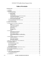
List of Tables
Table 1-1. Modem Models and Functions ..........................................................................................................................1-3
Table 1-2. Typical Signal Routing - Voice Mode ............................................................................................................... 1-11
Table 1-3. Relay Positions - VoiceView Mode .................................................................................................................. 1-11
Table 3-1. Bus Interface 176-Pin TQFP Pin Signals ...........................................................................................................3-5
Table 3-2. Bus Interface Pin Signal Definitions ...................................................................................................................3-7
Table 3-3. MDP Pin Signals - 144-Pin TQFP.................................................................................................................... 3-13
Table 3-4. MDP Pin Signal Definitions..............................................................................................................................3-15
Table 3-5. Current and Power Requirements ................................................................................................................... 3-18
Table 3-6. Maximum Ratings ...........................................................................................................................................3-18
Table 3-7. PCI Bus DC Specifications for 3.3V Signaling.................................................................................................. 3-19
Table 3-8. PCI Bus AC Specifications for 3.3V Signaling .................................................................................................. 3-19
Table 3-9. MDP Digital Electrical Characteristics .............................................................................................................. 3-20
Table 3-10. Analog Electrical Characteristics ................................................................................................................... 3-21
Table 3-11. Timing - Serial EEPROM Interface ................................................................................................................ 3-22
Table 3-12. Timing - External Device Bus Interface............................................................................. ............................. 3-23
Table 3-13. Timing - IOM-2 Interface ............................................................................................................................... 3-25
Table 4-1. Modem Pin Noise Characteristics......................................................................................................................4-3
Table 4-2. Crystal Specifications - Surface Mount ..............................................................................................................4-6
Table 4-3. Crystal Specifications - Through Hole................................................................................................................4-7
Table 5-1. PCI Configuration Registers ..............................................................................................................................5-1
Table 5-2. Command Register ...........................................................................................................................................5-2
Table 5-3. Status Register .................................................................................................................................................5-2
Table 5-4. BIF Address Map ..............................................................................................................................................5-3
Table 5-5. EEPROM Configuration Data ............................................................................................................................5-4
Table 6-1. Command Set Summary - Functional Use Sort .................................................................................................6-1
Table 6-2. Command Set Summary - Alphanumeric Sort ............................................................................. ......................6-4
vi
ROCKWELL PROPRIETARY INFORMATION
1129
RCV56HCF PCI/CardBus Modem Designer’s Guide
1. INTRODUCTION
1.1 SUMMARY
The Rockwell RCV56HCF-PCI Host-Controlled Modem Device Family supports high speed analog data, high speed fax,
ISDN, DSVD, AudioSpan, speakerphone, audio/voice, and VoiceView operation. It operates with PSTN or ISDN telephone
lines in the U.S. and world-wide and is offered in several device models (see Table 1-1).
The modem device set consists of PC PCI bus interface (BIF) and modem data pump (MDP) hardware available in two thin
quad flat packs (TQFPs). Host-controlled modem software is also provided.
Operating with +3.3V power, this device set supports 32-bit host applications in such designs as embedded motherboards,
PCI half cards, and CardBus cards.
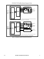
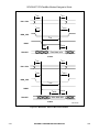
Figure 1-1 illustrates the general structure of the RCV56HCF software and the interface to the RCV56HCF hardware. Figure
1-2 illustrates the major hardware interfaces supported by each model.
The RCV56HCF employs a downloadable architecture so that the user can update MDP executable code.
Using K56flex technology, the RCV56HCF can receive data at speeds up to 56 kbps from a digitally connected K56flexcompatible central site modem, such as a Rockwell RC56CSM modem. K56flex modems take advantage of the PSTN which
is primarily digital except for the client modem to central office local loop and are ideal for applications such as remote
access to an Internet service provider (ISP), on-line service, or corporate site. The RCV56HCF can send data at speeds up
to V.34 rates.
In V.34 data mode, the modem operates at line speeds up to 33600 bps. Error correction (V.42/MNP 2-4) and data
compression (V.42 bis/MNP 5) maximize data transfer integrity and boost average data throughput. Non-error-correcting
mode is also supported.
AudioSpan (analog simultaneous audio/voice and data) operation supports a data rate with audio of 4.8 kbps.
SP models support position independent, full-duplex speakerphone (FDSP), as well as digital simultaneous voice and data
(DSVD) with speech coding per ITU-T G.729 Annex A with interoperable G.729 Annex B, and SIG DigiTalk DSVD.
The modem supports fax Group 3 send and receive rates up to 28800 bps and T.30 protocol.
V.80 and Rockwell Video Ready compatible synchronous access modes support host-controlled communication protocols, e.
g., H.324 video conferencing.
In voice/audio mode, PCM coding and decoding at 8000 Hz sample rate allows efficient digital storage of voice/audio. This
mode supports digital telephone answering machine, voice annotation, and audio recording/playback applications.
AccelerATor kits and reference designs are available to minimize application design time and costs.
This designer's guide describes the modem hardware capabilities and identifies the supporting commands. Commands and
parameters are defined in the RCVHCF Command Reference Manual (Order No. 1118).
1.2 FEATURES
• Data modem
− K56flex, 33.6 kbps, 31.2 kbps, V.34, V.32 bis, V.32, V.22 bis, V.22A/B, V.23, and V.21; Bell 212A and 103
− V.42 LAPM and MNP 2-4 error correction
− V.42 bis and MNP 5 data compression
− V.25 ter (Annex A) and EIA 602 command set
• Fax modem send and receive rates up to 28800 bps
− ITU-T V.34 fax*, V.17, V.29, V.27 ter, and V.21 ch 2
− EIA/TIA 578 Class 1, Class 1.0 (T.31) fax
• ISDN BRI support (option)*
− PC Bus support 2B+D channels
− IOM-2 interface to external U or S/T transceiver
− Simultaneous transfer of B1, B2, D channels (144 kbps; 64 kbps x 2, 16 kbps)
− V.34, DSVD, FDSP, audio functions over B channel
1129
ROCKWELL PROPRIETARY INFORMATION
1-1
RCV56HCF PCI/CardBus Modem Designer’s Guide
• AudioSpan (simultaneous audio/voice and data)*
− ITU-T V.61 modulation (4.8 kbps data plus audio)
− Handset, headset, or half-duplex speakerphone
• ITU-T V.70 DSVD (option)
− ITU-T G.729 Annex A with interoperable G.729 Annex B
− SIG (special interest group) DigiTalk DSVD
− Voice/silence detection and handset echo cancellation
− Handset, headset, or half-duplex speakerphone
• Full-duplex speakerphone (FDSP) mode
− Over PSTN or ISDN B channel (option)
− Switching to/from data, fax, DSVD and VoiceView
− Microphone gain and muting
− Speaker volume control and muting
− Adaptive line and acoustic echo cancellation
− Loop gain control, transmit and receive path AGC
− Acoustic echo cancellation concurrent with DSVD
− Noise suppression
− Room monitor
• V.80 and Rockwell Video Ready synchronous access modes support host-controlled communication protocols
− H.324 interface support
• V.8/V.8bis and supporting AT commands (V.25 ter with Annex A)
• Data/Fax/VoiceView/Voice call discrimination
• Voice, telephony, audio, VoiceView
− Voice (8-bit µ-Law compression/decompression)
− TIA-695 command set
− VoiceView alternating voice and data (option)
− 8-bit linear and 8-bit µ-Law record/playback
− 8.0 kHz, 11.025 kHz, 22.050 kHz and 44.1 kHz (down sampled to 11.025)
− Handset, acoustic, line echo cancellation
− Music on hold from host or analog hardware input
− TAM support with concurrent DTMF detect, ring detect and caller ID
• World-class operation (option)
− Call progress, blacklisting, multiple country support
• Integrated internal hybrid
• Caller ID and distinctive ring detect
• Modem and audio paths concurrent across PCI bus
• Single profile stored in host
• System compatibilities
− Windows 95 and Windows NT operating systems
− Microsoft's PC 97 Design Initiative compliant
− Unimodem/V compliant
• 32-bit PCI Local Bus interface
− Conforms to the PCI Local Bus Specification, Production Version, Revision 2.1
− PCI Bus Mastering interface to the MDP
− CardBus support with 512-byte RAM for CIS
− 33 MHz PCI clock support
• Device packages:
− Bus Interface in 176-pin TQFP
− MDP in 144-pin TQFP
• +3.3V operation
* See Note 6 in Table 1-1.
1-2
ROCKWELL PROPRIETARY INFORMATION
1129
RCV56HCF PCI/CardBus Modem Designer’s Guide
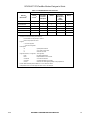
Table 1-1. Modem Models and Functions
Supported Functions
Marketing
K56flex,
V.34 Fax6
Voice/Audio/
VoiceView/
AudioSpan6
ISDN5,6
Full-duplex
Speakerphone
(FDSP)
and DSVD
W-Class
Model Number1
RCV56HCF/ISDN
Y
Y
Y
Y
–
RCV56HCFW/ISDN
Y
Y
Y
Y
Y
RCV56HCF/SP
Y
Y
–
Y
–
RCV56HCFW/SP
Y
Y
–
Y
Y
RC56HCF
Y
–
–
–
–
RC56HCFW
Y
–
–
–
Y
Notes:
1.
The two-device set manufacturing part numbers are:
PCI Bus Interface in 176-pin TQFP: 11229-XX.
MDP in 144-pin TQFP: R6776-XX.
2.
Legend:
Y = Function supported.
– = Function not supported.
3.
Model options:
SP
Speakerphone and DSVD.
V
Voice, audio, and VoiceView.
W
World-class (W-class).
4.
Supported functions (Y = Supported; – = Not supported):
FDSP
Full-duplex speakerphone.
DSVD
Digital simultaneous voice and data.
Voice/Audio
Voice and audio functions.
VoiceView
VoiceView alternating voice and data.
W-Class
World-class functions supporting multiple country requirements.
5.
Provides ISDN functionality with the addition of a U or S/T transceiver device.
6.
Initial production does not include support for ISDN, V.34 fax, and AudioSpan.
1129
ROCKWELL PROPRIETARY INFORMATION
1-3
RCV56HCF PCI/CardBus Modem Designer’s Guide
PC Software
Win32-based
communications
application
Win16-based
communications
application
MS-DOS
application
(MS-DOS Box)
Win32
NDIS
application
Win95
Communications Stack
RC56HCF
Serial Port Driver*
Modem Hardware
on Motherboard
or Plug-in Module
RC56HCF
WAN Miniport Driver*
RCV56HCF
Modem Device Set Hardware
Bus
Interface
(BIF)*
Modem
Data Pump
(MDP)*
* Rockwell supplied
1123F1 SO
Figure 1-1. RCV56HCF System Overview
1-4
ROCKWELL PROPRIETARY INFORMATION
1129
RCV56HCF PCI/CardBus Modem Designer’s Guide
RC56HCF MODEM DEVICE SET
VOICE*
DAA AND TELEPHONE
HANDSET INTERFACE
TXA
TELEPHONE
LINE
RXA
CID*
OH
HOST
INTERFACE
BUS
INTERFACE
(BIF)
MODEM
DATA PUMP
(MDP)
TELEPHONE
HANDSET*
RING
* OPTIONAL USE (SUPPORTED BY MODEL HARDWARE AND SOFTWARE).
a. Data/Fax - PSTN Configuration (RC56HCF and RC56HCFW)
DAA AND TELEPHONE
HANDSET INTERFACE
RCV56HCF MODEM DEVICE SET
TXA
TELEPHONE
LINE
RXA
CID*
OH
RING
HOST
INTERFACE
BUS
INTERFACE
(BIF)
MODEM
DATA PUMP
(MDP)
DC
FEED
LCS*
TELEPHONE
HANDSET
(OPTIONAL)
VOICE*
SPKR
MIC
AUDIO
INTERFACE
SPEAKER
MICROPHONE
* OPTIONAL USE (SUPPORTED BY MODEL HARDWARE AND SOFTWARE).
b. Data/Fax/Voice/Speakerphone, SVD - PSTN Configuration (RCV56HCF/SP and RCV56HCFW/SP)
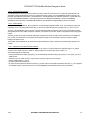
Figure 1-2. RCV56HCF Hardware Configuration Block Diagram
1129
ROCKWELL PROPRIETARY INFORMATION
1-5
RCV56HCF PCI/CardBus Modem Designer’s Guide
DAA AND TELEPHONE
HANDSET INTERFACE
RCV56HCF MODEM DEVICE SET
TXA
TELEPHONE
LINE
RXA
CID*
OH
RING
HOST
INTERFACE
BUS
INTERFACE
(BIF)
MODEM
DATA PUMP
(MDP)
DC
FEED
LCS*
TELEPHONE
HANDSET
(OPTIONAL)
VOICE*
SPKR*
MIC*
AUDIO
INTERFACE
(OPTIONAL)
ISDN
U OR S/T
INTERFACE
SPEAKER*
MICROPHONE*
ISDN LINE
* OPTIONAL USE (SUPPORTED BY MODEL HARDWARE AND SOFTWARE).
c. Data/Fax/Voice/Speakerphone, SVD/ISDN - PSTN and ISDN Configuration (RCV56HCF/ISDN and RCV56HCFW/ISDN)
RCV56HCF MODEM DEVICE SET
TELEPHONE
HANDSET INTERFACE
(OPTIONAL)
RING*
LCS
DC
FEED
TELEPHONE
HANDSET 1
DC
FEED
TELEPHONE
HANDSET 2
RING*
HOST
INTERFACE
BUS
INTERFACE
(BIF)
MODEM
DATA PUMP
(MDP)
LCS*
ISDN
U OR S/T
INTERFACE
ISDN LINE
* OPTIONAL USE (SUPPORTED BY MODEL HARDWARE AND SOFTWARE).
d. Data/Fax/Voice/Speakerphone, SVD/ISDN - ISDN Only Configuration (RCV56HCF/ISDN and RCV56HCFW/ISDN)
MD189F1 CONF
Figure 1-2. RCV56HCF Hardware Configuration Block Diagram (Continued)
1-6
ROCKWELL PROPRIETARY INFORMATION
1129
RCV56HCF PCI/CardBus Modem Designer’s Guide
1.3 TECHNICAL OVERVIEW
1.3.1 General Description
The RCV56HCF Device Set provides the processing core for a complete system design featuring data/fax modem, DSVD,
AudioSpan, speakerphone, voice/audio, and VoiceView depending on specific model (Table 1-1). Note: RCV56HCF Device
Set refers to the family of single device modem models listed in Table 1-1.
The modem is the full-featured, self-contained data modem/fax modem/DSVD/voice/audio/speakerphone solution. Dialing,
call progress, telephone line interface, AudioSpan, DSVD, speakerphone, voice/audio, and VoiceView functions are
supported and controlled through the command set.
The modem hardware connects to the host PC via a PCI bus interface. The OEM adds a crystal circuit, telephone line
interface, telephone interface (optional), audio interface (optional), and ISDN interface (optional) to complete the system.
1.3.2 Operating Modes
Data/Fax Modes
In K56flex mode, the modem can receive data from a digital source using a K56flex -compatible central site modem (e.
g., Rockwell RC56CSM) over the digital telephone network portion of the PSTN at line speeds up to 56 kbps. Asymmetrical
data transmission supports sending data at V.34 rates. This mode can fall back to full-duplex V.34 mode, and to slower rates
as supported by line conditions.
In V.34 data modem mode, the modem can also operate in 2-wire, full-duplex, asynchronous modes at line rates up to
33600 bps. Data modem modes perform complete handshake and data rate negotiations. Using V.34 modulation to optimize
modem configuration for line conditions, the modem can connect at the highest data rate that the channel can support from
33600 bps to 2400 bps with automatic fallback. Automode operation in V.34 is provided in accordance with PN3320 and in
V.32 bis in accordance with PN2330. All tone and pattern detection functions required by the applicable ITU or Bell standard
are supported.
In fax modem modes, the modem fully supports Group 3 facsimile send and receive speeds of 28800, 14400, 12000, 9600,
7200, 4800, or 2400 bps. Fax modes support Group 3 fax requirements. Fax data transmission and reception performed by
the modem are controlled and monitored through the fax EIA-578 Class 1 command interface. Full HDLC formatting, zero
insertion/deletion, and CRC generation/checking are provided.
Both transmit and receive fax data are buffered within the modem. Data transfer to and from the DTE is flow controlled by
XON/XOFF and RTS/CTS.
AudioSpan Modes
AudioSpan provides full-duplex analog simultaneous audio/voice and data over a single telephone line at a data rate with
audio of 4800 bps using V.61 modulation. AudioSpan can send any type of audio waveform, including music. Data can be
sent with or without error correction. The audio/voice interface can be in the form of a headset, handset, or microphone and
speaker (half-duplex speakerphone). Handset echo cancellation is provided.
Host-Controlled DSVD Mode (ISDN and SP Models)
ISDN and SP models support host-controlled DSVD. A microphone and a speaker are required.
ITU-T interoperable G.729 and G.729 Annex A with interoperable G.729 Annex B Operation. Voice activity detection
supports speech coding at an average bit rate significantly lower than 8.0 kbps.
SIG DigiTalk. Speech coding is performed at 8.5 kbps.
Voice/Audio Mode (V Models)
Voice/Audio Mode features include 8-bit linear and 8-bit µ-Law coding/decoding, tone detection/generation and call
discrimination, concurrent DTMF detection, and 8-bit monophonic audio data encoding at 11.025 kHz or 8000 Hz.
Voice/Audio Mode is supported by three submodes:
1.
Online Voice Command Mode supports connection to the telephone line or a voice/audio I/O device (e.g., microphone,
speaker, or handset).
2.
Voice Receive Mode supports recording voice or audio data input at the MIC_M pin, typically from a
microphone/handset or the telephone line.
3.
Voice Transmit Mode supports playback of voice or audio data to the TXA1_L1/TXA2_L1 output, typically to a
speaker/handset or to the telephone line.
1129
ROCKWELL PROPRIETARY INFORMATION
1-7
RCV56HCF PCI/CardBus Modem Designer’s Guide
Speakerphone Mode (ISDN and SP Models)
The speakerphone mode features an advanced proprietary speakerphone algorithm which supports full-duplex voice
conversation with both acoustic and line echo cancellation. Parameters are constantly adjusted to maintain stability with
automatic fallback from full-duplex to pseudo-duplex operation. The speakerphone algorithm allows position independent
placement of microphone and speaker.
The speakerphone mode provides hands-free full-duplex telephone operation under host control. The host can separately
control volume, muting, and AGC in microphone and speaker channels.
Synchronous Access Mode (SAM)
V.80 and Rockwell Video Ready synchronous access modes between the modem and the host/DTE are provided for hostcontrolled communication protocols, e.g., H.324 video conferencing applications.
Voice-call-first (VCF) before switching to a videophone call is also supported.
1.3.3 Host-Controlled Modem Software
Host-controlled modem software performs processing of general modem control, command sets, fax Class 1, AudioSpan,
DSVD, speakerphone, voice/audio/TAM, error correction, data compression, and operating system interface functions.
Configurations of the modem software are provided to support modem models listed in Table 1-1.
Binary executable modem software is provided for the OEM.
1.3.4 Downloadable Modem Data Pump Firmware
Binary executable code controlling MDP operation is downloaded as required during operation.
1.3.5 Hardware Interfaces
1.3.5.1 PCI Bus Host Interface
The Bus Interface conforms to the PCI Local Bus Specification, Production Version, Revision 2.1, June 1, 1995. It is a
memory slave (burst transactions) and a bus master for PC host memory accesses (burst transactions). Configuration is by
PCI configuration protocol.
The following interface signals are supported:
• Address and data
− 32 bidirectional Address/Data (AD[31-0]; bidirectional
− Four Bus Command and Byte Enable (CBE [3:0]), bidirectional
− Bidirectional Parity (PAR); bidirectional
• Interface control
− Cycle Frame (FRAME#); bidirectional
− Initiator Ready (IRDY#); bidirectional
− Target Ready (TRDY#); bidirectional
− Stop (STOP#); bidirectional
− Initialization Device Select (IDSEL); input
− Device Select (DEVSEL#); bidirectional
• Arbitration
− Request (REQ#); output
− Grant (GRANT#); input
• Error reporting
− Parity Error ((PERR#); bidirectional
− System Error ; bidirectional
• Interrupt
− Interrupt A (INTA#); output
• System
− Clock (PCICLK); input
− Reset (PCIRST#); input
− Clock Running (CLKRUN#); input
1-8
ROCKWELL PROPRIETARY INFORMATION
1129
RCV56HCF PCI/CardBus Modem Designer’s Guide
1.3.5.2 Serial EEPROM Interface
A serial EEPROM is required to store the Maximum Latency, Minimum Grant, Device ID, Vendor ID, Subsystem ID, and
Subsystem Vendor ID parameters for the PCI Configuration Space Header. The serial EEPROM interface connects to an
Microchip 93LC66B, Atmel AT93C66, or equivalent 256 x 16 serial EEPROM. The interface signals are: a serial data input
line from the EEPROM (SROMIN), a serial data output line to the EEPROM (SROMOUT), Clock to the EEPROM
(SROMCLK), and chip select to the EEPROM (SROMCS). The EEPROM is programmable by the PC via the BIF.
1.3.5.3 Audio Interface
One Speaker output (SPKROUT_M) is provided for an optional OEM-supplied speaker circuit. Two microphone inputs are
supported: one for Voice Microphone input (MIC_V) and one for Music Microphone input (MIC_M), e.g., music-on-hold.
The MIC_V and SPKROUT_M lines connect to the handset and speaker to support functions such as AudioSpan headset
and speakerphone modes, FDSP, telephone emulation, microphone voice record, speaker voice playback, and call progress
monitor.
The MIC_M input can accept an external audio signal to support the music-on-hold function and routes it to the telephone
line. If music-on-hold function is not required, the microphone signal can be connected to the MIC_M input to support
telephone emulation mode.
The Speaker output (SPKROUT_M) carries the normal speakerphone audio or reflects the received analog signals in the
modem.
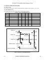
1.3.5.4 Telephone Line/Telephone/Audio Interface
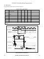
The Telephone Line/Telephone/Audio Signal Interface can support a 3-relay telephone line interface (Figure 1-3). Signal
routing for Voice mode is shown in Table 1-2. Relay positions for VoiceView are shown in Table 1-3.
The following signals are supported:
• A single-ended Receive Analog input (RXA_L1) and a differential Transmit Analog output (TXA1_L1 and TXA2_L1) to the
telephone line.
• Off-hook (OH_L1#), Caller ID (CID_L1#), and Voice (VOICE_L1#) relay control outputs.
• A Ring Indicate (IRING_L1) input.
• A Loop Current Sense (LCS) input.
• An input from the telephone microphone (TELIN_L1) and an output to the telephone speaker (TELOUT_L1 ) are supported
in AudioSpan modes. These lines connect voice record/playback and AudioSpan audio to the local handset.
1129
ROCKWELL PROPRIETARY INFORMATION
1-9
RCV56HCF PCI/CardBus Modem Designer’s Guide
LCS_L1#
IRING_L1#
VOICE#
OH_L1#
CID_L1#
VC_L1
TXA1_L1
TXA2_L1
RXA_L1
HYBRD
&
XFRMR
SSI
&
BRDGE
CALLID
RELAY
SURG
PROT
OH
RELAY
TELOUT_L1
RCV56HCF
MODEM
DEVICE
TELIN_L1
TEL LINE
CUR
SRC
HANDSET
HYBRID
TEL HANDSET
RNG
DET
VOICE
RELAY
LCS
TELEPHONE LINE/TELEPHONE HANDSET
INTERFACE CIRCUIT
MIC_M
MIC_V
SPKROUT_M
BIAS
AMP/
SOUNDUCER
(OPTIONAL)
MICROPHONE
HEADPHONE
AUDIO/HEADPHONE
INTERFACE CIRCUIT
1123F1-3 AIF 3R-US
Figure 1-3. Typical Audio Signal Interface (U.S.)
1-10
ROCKWELL PROPRIETARY INFORMATION
1129
RCV56HCF PCI/CardBus Modem Designer’s Guide
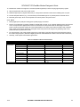
Table 1-2. Typical Signal Routing - Voice Mode
+VLS=
Command
Description
Input Selected
Output Selected
VOICE# CID_L1#
OH_L1#
Output
Output
Output
Activated Activated Activated
0
Modem on hook. Phone connected to Line
.
.
No
No
Yes
1
Modem connected to Line.
RXA_L1
TXA1/2_L1
Yes
Yes
No
2
Modem connected to Handset
TELIN_L1
TELOUT_L1
No
Yes
Yes
3
Modem connected to Line and Handset
RXA_L1
TXA
Yes
No
No
4
Modem connected to Speaker
SPKROUT_M
No
No
Yes
5
Modem connected to Line and Speaker
RXA_L1
TXA1/2_L1, SPKROUT_M Yes
Yes
No
6
Modem connected to Microphone
MIC_V
.
No
Yes
7
Speaker and Mic. routed to Line via Modem
RXA_L1, MIC_M TXA1/2_L1, SPKROUT_M Yes
Yes
No
8
Modem connected to Speaker
.
SPKROUT_M
No
Yes
9
Modem connected to Line and Speaker
RXA_L1
TXA1/2_L1, SPKROUT_M Yes
Yes
No
10
Speaker and Mic. routed to Line via Modem
RXA_L1, MIC_M TXA1/2_L1, SPKROUT_M Yes
Yes
No
11
Modem connected to Microphone
MIC_V
No
Yes
12
Speaker and Mic. routed to Line via Modem
RXA_L1, MIC_M TXA1/2_L1, SPKROUT_M Yes
Yes
No
13
Speaker and Mic. routed to Line via Modem
RXA_L1, MIC_M TXA1/2_L1, SPKROUT_M Yes
Yes
No
14
Modem connected to Headset
MIC_V
No
Yes
15
Speaker and Mic. routed to Line via Modem
RXA_L1, MIC_M TXA1/2_L1, SPKROUT_M Yes
Yes
No
No
.
No
No
SPKROUT_M
No
Table 1-3. Relay Positions - VoiceView Mode
2-Relay DAA
Stage
1129
Off-Hook Relay (OH_L1)
Activated
Voice Relay (VOICE#)
Activated
Function
1
On-hook
No
No
2a
Detected tone - on-hook
No
No
2b
Detected tone - off-hook for handset and speakerphone
Yes
No
3
Off-hook
Yes
Yes
ROCKWELL PROPRIETARY INFORMATION
1-11
RCV56HCF PCI/CardBus Modem Designer’s Guide
This page is intentionally blank.
1-12
ROCKWELL PROPRIETARY INFORMATION
1129
RCV56HCF PCI/CardBus Modem Designer’s Guide
2. TECHNICAL SPECIFICATIONS
2.1 ESTABLISHING DATA MODEM CONNECTIONS
Dialing
DTMF Dialing. DTMF dialing using DTMF tone pairs is supported in accordance with ITU-T Q.23. The transmit tone level
complies with Bell Publication 47001.
Pulse Dialing. Pulse dialing is supported in accordance with EIA/TIA-496-A.
Blind Dialing. The modem can blind dial in the absence of a dial tone if enabled by the X0, X1, or X3 command.
Modem Handshaking Protocol
If a tone is not detected within the time specified in the S7 register after the last digit is dialed, the modem aborts the call
attempt.
Call Progress Tone Detection
Ringback, equipment busy, and progress tones can be detected in accordance with the applicable standard.
Answer Tone Detection
Answer tone can be detected over the frequency range of 2100 ± 40 Hz in ITU-T modes and 2225 ± 40 Hz in Bell modes.
Ring Detection
A ring signal can be detected from a TTL-compatible square wave input (frequency is country-dependent).
Billing Protection
When the modem goes off-hook to answer an incoming call, both transmission and reception of data are prevented for a
period of time determined by country requirement to allow transmission of the billing signal.
Connection Speeds
Data modem line connection can be selected using the +MS command in accordance with V.25 ter. The +MS command
selects modulation, enables/disables automode, and selects transmit and receive minimum and maximum line speeds.
Automode
Automode detection can be enabled by the +MS command to allow the modem to connect to a remote modem in
accordance with V.25 ter.
2.2 DATA MODE
Data mode exists when a telephone line connection has been established between modems and all handshaking has been
completed.
Speed Buffering (Normal Mode)
Speed buffering allows a DTE to send data to, and receive data from, a modem at a speed different than the line speed. The
modem supports speed buffering at all line speeds.
DTE-to-Modem Flow Control
If the modem-to-line speed is less than the DTE-to-modem speed, the modem supports XOFF/XON or RTS/CTS flow control
with the DTE to ensure data integrity.
Escape Sequence Detection
The “+++” escape sequence can be used to return control to the command mode from the data mode. Escape sequence
detection is disabled by an S2 Register value greater than 127.
GSTN Cleardown (K56flex, V.34, V.32 bis, V.32)
Upon receiving GSTN Cleardown from the remote modem in a non-error correcting mode, the modem cleanly terminates the
call.
1129
ROCKWELL PROPRIETARY INFORMATION
2-1
RCV56HCF PCI/CardBus Modem Designer’s Guide
Fall Forward/Fallback (K56flex, V.34/V.32 bis/V.32)
During initial handshake, the modem will fallback to the optimal line connection within K56flex/V.34/V.32 bis/V.32 mode
depending upon signal quality if automode is enabled by the +MS command.
When connected in K56flex/V.34/V.32 bis/V.32 mode, the modem will fall forward or fallback to the optimal line speed within
the current modulation depending upon signal quality if fall forward/fallback is enabled by the %E1 command.
Retrain
The modem may lose synchronization with the received line signal under poor line conditions. If this occurs, retraining may
be initiated to attempt recovery depending on the type of connection.
The modem initiates a retrain if line quality becomes unacceptable if enabled by the %E command. The modem continues to
retrain until an acceptable connection is achieved, or until 30 seconds elapse resulting in line disconnect.
2.3 ERROR CORRECTION AND DATA COMPRESSION
V.42 Error Correction
V.42 supports two methods of error correction: LAPM and, as a fallback, MNP 4. The modem provides a detection and
negotiation technique for determining and establishing the best method of error correction between two modems.
MNP 2-4 Error Correction
MNP 2-4 is a data link protocol that uses error correction algorithms to ensure data integrity. Supporting stream mode, the
modem sends data frames in varying lengths depending on the amount of time between characters coming from the DTE.
V.42 bis Data Compression
V.42 bis data compression mode operates when a LAPM or MNP connection is established.
The V.42 bis data compression employs a “string learning” algorithm in which a string of characters from the DTE is encoded
as a fixed length codeword. Two dictionaries, dynamically updated during normal operation, are used to store the strings.
MNP 5 Data Compression
MNP 5 data compression mode operates during an MNP connection.
In MNP 5, the modem increases its throughput by compressing data into tokens before transmitting it to the remote modem,
and by decompressing encoded received data before sending it to the DTE.
2.4 MNP 10EC™ ENHANCED CELLULAR CONNECTION
A traditional landline modem, when used for high-speed cellular data transmission, typically encounters frequent signal
interference and degradation in the connection due to the characteristics of the analog cellular network. In this case, cellularspecific network impairments, such as non-linear distortion, fading, hand-offs, and high signal-to-noise ratio, contribute to an
unreliable connection and lower data transfer performance. Implementations relying solely on protocol layer methods, such
as MNP 10, generally cannot compensate for the landline modem's degraded cellular channel performance.
The modem achieves higher cellular performance by implementing enhanced cellular connection techniques at both the
physical and protocol layers, depending on modem model. The modem enhances the physical layer within the modulation by
optimizing its responses to sudden changes in the cellular connection. The MNP 10EC protocol layer implemented in the
modem software improves data error identification/correction and maximizes data throughput by dynamically adjusting speed
and packet size based on signal quality and data error performance.
2.5 FAX CLASS 1 OPERATION
Facsimile functions operate in response to fax class 1 commands when +FCLASS=1.
In the fax mode, the on-line behavior of the modem is different from the data (non-fax) mode. After dialing, modem operation
is controlled by fax commands. Some AT commands are still valid but may operate differently than in data modem mode.
Calling tone is generated in accordance with T.30.
2.6 VOICE/AUDIO MODE
Voice and audio functions are supported by the Voice Mode. Voice Mode includes three submodes: Online Voice Command
Mode, Voice Receive Mode, and Voice Transmit Mode.
2-2
ROCKWELL PROPRIETARY INFORMATION
1129
RCV56HCF PCI/CardBus Modem Designer’s Guide
2.6.1 Online Voice Command Mode
This mode results from the connection to the telephone line or a voice/audio I/O device (e.g., microphone, speaker, or
handset) through the use of the +FCLASS=8 and +VLS commands. After mode entry, AT commands can be entered without
aborting the connection.
2.6.2 Voice Receive Mode
This mode is entered when the +VRX command is active in order to record voice or audio data input at the RXA_L1 pin,
typically from a microphone/handset or the telephone line.
Received analog voice samples are converted to digital form and compressed for reading by the host. AT commands control
the codec bits-per-sample rate.
Received analog mono audio samples are converted to digital form and formatted into 8-bit unsigned linear or µ-Law PCM
format for reading by the host. AT commands control the bit length and sampling rate. Concurrent DTMF/tone detection is
available.
2.6.3 Voice Transmit Mode
This mode is entered when the +VTX command is active in order to playback voice or audio data to the TXA1_L1 output,
typically to a speaker/handset or to the telephone line. Digitized audio data is converted to analog form then output to the
TXA1_L1 output.
2.6.4 Tone Detectors
The tone detector signal path is separate from the main received signal path thus enabling tone detection to be independent
of the configuration status. In Tone Mode, all three tone detectors are operational.
2.6.5 Speakerphone Modes
Speakerphone modes are selected in voice mode with the following commands:
Speakerphone ON/OFF (+VSP). This command turns the Speakerphone function ON (+VSP = 1) or OFF (+VSP = 0).
Microphone Gain (+VGM)=<gain>. This command sets the microphone gain of the Speakerphone function. <gain> is an
unsigned octet where values greater than 128 indicate a gain larger than nominal and values smaller than 128 indicate a
gain smaller than nominal.
Speaker Gain (+VGS=<gain>). This command sets the speaker gain of the Speakerphone function. <gain> is an unsigned
octet where values greater than 128 indicate a gain larger than nominal and values smaller than 128 indicate a gain smaller
than normal.
2.7 SIMULTANEOUS AUDIO/VOICE AND DATA (AudioSpan)
The modem can operate in AudioSpan Mode if the remote modem is also configured for AudioSpan Mode operation.
AT commands are used to select the AudioSpan Mode, to enable automatic AudioSpan modulation selection or select a
specific AudioSpan modulation, and to enable AudioSpan data burst operation.
V.61 modulation supports 4800 bps data speed with audio, and a data-only speed of 4800 bps.
The AudioSpan audio interface defaults to the local handset connected to the modem and can be configured to interface
through the modem microphone and speaker pins to support use of a headset or a speakerphone.
2.8 HOST-BASED DSVD MODE
Host-based DSVD operation is enabled by the -SSE or -SMS command. In Host-based DSVD Mode, the modem supports
the transfer of data and voice occurs simultaneously during a data connection.
2.9 FULL-DUPLEX SPEAKERPHONE (FDSP) MODE
The modem operates in FDSP mode when +FCLASS=8 and +VSP=1 (see 2.6.5).
In FDSP Mode, speech from a microphone or handset is converted to digital form, shaped, and output to the telephone line
through the line interface circuit. Speech received from the telephone line is shaped, converted to analog form, and output to
the speaker or handset. Shaping includes both acoustic and line echo cancellation.
2.10 VOICEVIEW
Voice and data can be alternately sent and received in a time-multiplexed fashion over the telephone line whenever the
+FCLASS=80 command is active. This command and other VoiceView commands embedded in host communications
1129
ROCKWELL PROPRIETARY INFORMATION
2-3
RCV56HCF PCI/CardBus Modem Designer’s Guide
software control modem operation. Most VoiceView commands use an extended syntax starting with the characters "-S",
which signifies the capability to switch between voice and data.
2.11 CALLER ID
Caller ID can be enabled/disabled using the +VCID command. When enabled, caller ID information (date, time, caller code,
and name) can be passed to the DTE in formatted or unformatted form. Inquiry support allows the current caller ID mode
and mode capabilities of the modem to be retrieved from the modem.
2.12 WORLD CLASS COUNTRY SUPPORT
The W-class models include functions which support modem operation in multiple countries. The following capabilities are
provided in addition to the data modem functions previously described. Country dependent parameters are included in the
.INF file for customization by the OEM.
2.12.1 Programmable Parameters
The following parameters are programmable:
• Dial tone detection levels and frequency ranges.
• DTMF dialing transmit output level, DTMF signal duration, and DTMF interdigit interval parameters.
• Pulse dialing parameters such as make/break times, set/clear times, and dial codes.
• Ring detection frequency range.
• Blind dialing disable/enable.
• The maximum, minimum, and default carrier transmit level values.
• Calling tone, generated in accordance with V.25, may also be disabled.
• Call progress frequency and tone cadence for busy, ringback, congested, dial tone 1, and dial tone 2.
• Answer tone detection period.
• On-hook/off-hook, make/break, and set/clear relay control parameters.
2.12.2 Blacklist Parameters
The modem can operate in accordance with requirements of individual countries to prevent misuse of the network by limiting
repeated calls to the same number when previous call attempts have failed. Call failure can be detected for reasons such as
no dial tone, number busy, no answer, no ringback detected, voice (rather than modem) detected, and key abort (dial
attempt aborted by user). Actions resulting from such failures can include specification of minimum inter-call delay, extended
delay between calls, and maximum numbers of retries before the number is permanently forbidden ("blacklisted"). Up to 20
such numbers may be tabulated. The blacklist parameters are programmable.
2.13 DIAGNOSTICS
2.13.1 Commanded Tests
Diagnostics are performed in response to &T commands per V.54.
Analog Loopback (&T1 Command). Data from the local DTE is sent to the modem, which loops the data back to the local
DTE.
Analog Loopback with Self Test (&T8 Command). An internally generated test pattern of alternating 1s and 0s (reversals)
is sent to the modem. An error detector within the modem checks for errors in the string of reversals.
Remote Digital Loopback (RDL) (&T6 Command). Data from the local DTE is sent to the remote modem which loops the
data back to the local DTE.
Remote Digital Loopback with Self Test (&T7 Command). An internally generated pattern is sent from the local modem
to the remote modem, which loops the data back to the local modem.
Local Digital Loopback (&T3 Command). When local digital loop is requested by the local DTE, two data paths are set up
in the local modem. Data from the local DTE is looped back to the local DTE (path 1) and data received from the remote
modem is looped back to the remote modem (path 2).
2.13.2 Power On Reset Tests
Upon power on, an MDP test is performed. If the MDP is not operational, an error indication is generated.
2.14 LOW POWER SLEEP MODE
When not being used, the MDP is placed in a low power state.
2-4
ROCKWELL PROPRIETARY INFORMATION
1129
RCV56HCF PCI/CardBus Modem Designer’s Guide
3. HARDWARE INTERFACE
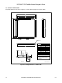
3.1 HARDWARE SIGNAL PINS AND DEFINITIONS
The RCV56HCF (PCI) functional interface signals are shown in Figure 3-1.
The Bus Interface hardware interface signals are shown by major interface in Figure 3-2.
The Bus Interface pin assignments for the 176-pin TQFP are shown Figure 3-3 and are listed Table 3-1.
The Bus Interface hardware interface signals are defined in Table 3-2.
The MDP hardware interface signals are shown by major interface in Figure 3-4.
The MDP pin assignments for the 144-pin TQFP are shown in Figure 3-5 and are listed in Table 3-3.
The MDP hardware interface signals are defined in Table 3-4.
1129
ROCKWELL PROPRIETARY INFORMATION
3-1
RCV56HCF PCI/CardBus Modem Designer’s Guide
AD[31:0]
CBE0#
CBE1#
CBE2#
CBE3#
PCICLK
PCIRST#
FRAME#
IDSEL
DEVSEL#
IRDY#
TRDY#
PAR
REQ#
GNT#
INTA#
STOP#
PERR#
SERR#
PCI
BUS
28.224 MHZ
CRYSTAL
CIRCUIT
XIN
XOUT
SROMCLK
SROMCS
SROMIN
SROMOUT
256 x 16
PCI
SERIAL
EEPROM
VDD
AVDD
GND
GND
AGND
AGND
AGND
VDD
AVDD_IA
OH_L1#
CID_L1#
VOICE#
MUTE_L1#
IRING_L1#
LCS_L1#
RH_L1#
USED_L1
LCS_H1#
ORING_H1
LCS_H2#
ORING_H2
I/O[4:0]
RCV56HCF
BUS INTERFACE
(176-TQFP)
[11229]
AND
RCV56HCF
MDP
(144-PIN TQFP)
[R6776]
UNIVERSAL
DAA AND
TELEPHONE
INTERFACE
TELIN_L1
TELOUT_L1
RXA_L1
TXA1_L1
TXA2_L1
VC_L1
SPKROUT_M
MIC_M
MIC_V
AUDIO
INTERFACE
IOM_FRAME
IOM_CLK
IOM_DD
IOM_DU
DA[4:0]
GND
GND_IA
AGND
AGND_V1
AGND_M1
DD[7:0]
DRD#
DWR#
ISDN_CS#
ISDN_INT#
DRESET
DRESET#
ISDN
U OR S/T
INTERFACE
(OPTIONAL)
MD189F2 ISF
Figure 3-1. RCV56HCF Interface Signals
3-2
ROCKWELL PROPRIETARY INFORMATION
1129
RCV56HCF PCI/CardBus Modem Designer’s Guide
27pF
5%
28.224 MHz
27pF
5%
PCI
BUS
EEPROM
NC
1K
GND
1K
VDD
132
XIN
131
XOUT
27
25
62
46
66
63
64
86
73
61
43
98
97
96
95
92
91
90
89
85
84
81
80
79
78
75
74
59
58
57
56
53
52
51
50
42
41
40
37
36
35
34
32
72
30
29
24
67
68
69
13
10
11
12
19
20
21
22
23
2
3
6
7
8
14
15
45
151
152
153
160
162
174
175
PCICLK
PCIRST#
FRAME#
IDSEL
DEVSEL#
IRDY#
TRDY#
CBE0#
CBE1#
CBE2#
CBE3#
AD0
AD1
AD2
AD3
AD4
AD5
AD6
AD7
AD8
AD9
AD10
AD11
AD12
AD13
AD14
AD15
AD16
AD17
AD18
AD19
AD20
AD21
AD22
AD23
AD24
PCI
AD25
AD26
AD27
AD28
AD29
AD30
AD31
PAR
REQ#
GNT#
INTA#
STOP#
PERR#
SERR#
SROMCLK
SROMCS
SROMIN
SROMOUT
NC
NC
NC
NC
NC
RESERVED
RESERVED
RESERVED
RESERVED
RESERVED
RESERVED
RESERVED
RESERVED
RESERVED
RESERVED
RESERVED
RESERVED
RESERVED
RESERVED
RESERVED
1M
31
9
CLKRUN#
CARDBUS#
MODEM_CS#
MODEM_IRQ
M_TXCLK
M_TX
M_RXCLK
M_RX
WKRES#
SI_FRAME
SI_CLK
SI_DD
SI_DU
M_CLK
L85CLK
M_RXOUT
M_SCLK
M_STROBE
M_CTRL
M_TXSIN
V_RXOUT
V_SCLK
V_STROBE
V_CTRL
V_TXSIN
OH_L1#
CID_L1#
VOICE#
MUTE_L1#
IRING_L1#
LCS_L1#
RH_L1#
USED_L1
LCS_H1#
ORING_H1
LCS_H2#
ORING_H2
I/O0
I/O1
I/O2
I/O3
I/O4
DA0
DA1
BUS INTERFACE DA2
DA3
176-TQFP
DA4
[11229]
DD0
DD1
DD2
DD3
DD4
DD5
DD6
DD7
DRD#
DWR#
DRESET#
DRESET
ISDN_CS#
ISDN_INT#
113
135
106
105
108
136
107
103
102
100
101
147
130
144
145
143
148
146
141
140
142
138
139
167
166
165
164
170
171
161
173
172
163
174
162
158
157
156
155
154
118
117
116
115
114
128
127
126
125
124
123
122
121
111
112
104
137
16
17
VIO1
VIO2
VDD
VDD
VDD
VDD
VDD
VDD
VDD
VDD
VDD
VDD
VDD
VDD
VDD
VDD
VDD
VDD
VGG1
44
47
5
26
38
49
55
70
76
88
94
110
119
149
168
83
1
133
134
GND
GND
GND
GND
GND
GND
GND
GND
GND
GND
GND
GND
GND
GND
GND
GND
GND
GND
GND
GND
GND
GND
4
18
176
28
33
39
48
54
60
65
71
77
82
87
93
99
109
120
129
150
159
169
MDP
DAA
MDP AND
ISDN U OR S/T
INTERFACE
ISDN U OR S/T
INTERFACE
3.3 V
VDD
GND
MD189F3 11221HS-176TQFP
Figure 3-2. Bus Interface 176-Pin TQFP Hardware Interface Signals
1129
ROCKWELL PROPRIETARY INFORMATION
3-3
VDD
RESERVED
RESERVED
GND
VDD
RESERVED
RESERVED
RESERVED
CARDBUS#
SROMCS
SROMIN
SROMOUT
SROMCLK
RESERVED
RESERVED
ISDN_CS#
ISDN_INT#
GND
NC
NC
NC
NC
NC
INTA#
PCIRST#
VDD
PCICLK
GND
GNT#
REQ#
CLKRUN#
AD31
GND
AD30
AD29
AD28
AD27
VDD
GND
AD26
AD25
AD24
ORING_H1
ORING_H2
RH_L1#
RESERVED
GND
I/O0
I/O1
I/O2
I/O3
I/O4
RESERVED
RESERVED
RESERVED
GND
VDD
RESERVED
RESERVED
RESERVED
RESERVED
RESERVED
RESERVED
RESERVED
RESERVED
RESERVED
RESERVED
RESERVED
RESERVED
M_RX
MODEM_IRQ
VGG1
VDD
VOICE#
MUTE_L1#
OH_L1#
CID_L1#
132
131
130
129
128
127
126
125
124
123
122
121
120
119
118
117
116
115
114
113
112
111
110
109
108
107
106
105
104
103
102
101
100
99
98
97
96
95
94
93
92
91
90
89
XIN
XOUT
MODEM_CLK
GND
DD0
DD1
DD2
DD3
DD4
DD5
DD6
DD7
GND
VDD
DA0
DA1
DA2
DA3
DA4
MODEM_CS#
DWR#
DRD#
VDD
GND
M_RXCLK
WKRES#
M_TXCLK
M_TX
DRESET#
SI_FRAME
SI_CLK
SI_DU
SI_DD
GND
AD0
AD1
AD2
AD3
VDD
GND
AD4
AD5
AD6
AD7
AD17
AD16
GND
CBE2#
FRAME#
IRDY#
TRDY#
GND
DEVSEL#
STOP#
PERR#
SERR#
VDD
GND
PAR
CBE1#
AD15
AD14
VDD
GND
AD13
AD12
AD11
AD10
GND
VDD
AD9
AD8
CBE0#
GND
VDD
AD19
AD18
GND
VDD
RESERVED
IDSEL
VIO2
GND
VDD
AD23
AD22
AD21
AD20
45
46
47
48
49
50
51
52
53
54
55
56
57
58
59
60
61
62
63
64
65
66
67
68
69
70
71
72
73
74
75
76
77
78
79
80
81
82
83
84
85
86
87
88
CBE3#
VIO1
1
2
3
4
5
6
7
8
9
10
11
12
13
14
15
16
17
18
19
20
21
22
23
24
25
26
27
28
29
30
31
32
33
34
35
36
37
38
39
40
41
42
43
44
176
175
174
173
172
171
170
169
168
167
166
165
164
163
162
161
160
159
158
157
156
155
154
153
152
151
150
149
148
147
146
145
144
143
142
141
140
139
138
137
136
135
134
133
GND
RESERVED
LCS_H2#
USED_L1
LCS_H1#
LCS_L1#
IRING_L1#
GND
VDD
RCV56HCF PCI/CardBus Modem Designer’s Guide
MS189F4-BIF-PO-176TQFP
Figure 3-3. Bus Interface 176-Pin TQFP Pin Signals
3-4
ROCKWELL PROPRIETARY INFORMATION
1129
RCV56HCF PCI/CardBus Modem Designer’s Guide
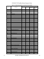
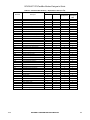
Table 3-1. Bus Interface 176-Pin TQFP Pin Signals
Pin
1
2
3
4
5
6
7
8
9
10
11
12
13
14
15
16
17
18
19
20
21
22
23
24
25
26
27
28
29
30
31
32
33
34
35
36
37
38
39
40
41
42
43
44
45
46
47
48
49
50
51
52
53
54
55
56
57
58
59
60
61
62
63
64
1129
Signal Label
VDD
RESERVED
RESERVED
GND
VDD
RESERVED
RESERVED
RESERVED
CARDBUS#
SROMCS
SROMOUT
SROMIN
SROMCLK
RESERVED
RESERVED
ISDN_CS#
ISDN_INT#
GND
NC
NC
NC
NC
NC
INTA#
PCIRST#
VDD
PCICLK
GND
GNT#
REQ#
CLKRUN#
AD31
GND
AD30
AD29
AD28
AD27
VDD
GND
AD26
AD25
AD24
CBE3#
VIO1
RESERVED
IDSEL
VIO2
GND
VDD
AD23
AD22
AD21
AD20
GND
VDD
AD19
AD18
AD17
AD16
GND
CBE2#
FRAME#
IRDY#
TRDY#
I/O
P
I
I
G
P
O
O
O
I
O
O
I
O
O
I
O
I
G
I
I
I
O
I
O
I
P
I
G
I
O
I
I/O
G
I/O
I/O
I/O
I/O
P
G
I/O
I/O
I/O
I/O
P
I
I
P
G
P
I/O
I/O
I/O
I/O
G
P
I/O
I/O
I/O
I/O
G
I/O
I/O
I/O
I/O
I/O Type1
PWR
It
It
GND
PWR
Ot2
Ot2
Ot2
PWR
Ot2
Ot2
It
Ot2
Ot2
It
Ot2
It
GND
Itpd
It
It
Ot4ts
It
Opod
Ip
PWR
Ip
GND
Ipts
Opts
It
I/Opts
GND
I/Opts
I/Opts
I/Opts
I/Opts
PWR
GND
I/Opts
I/Opts
I/Opts
I/Opts
PWR
Itpd
Ip
PWR
GND
PWR
I/Opts
I/Opts
I/Opts
I/Opts
GND
PWR
I/Opts
I/Opts
I/Opts
I/Opts
GND
I/Opts
I/Opsts
I/Opsts
I/Opsts
Interface
To 3.3V
To GND
To GND
Ground
To 3.3V
NC
NC
NC
VCC through 10KΩ for PCI
SROM Chip Select
SROM Data Out
SROM Data In
SROM Clock
NC
To GND
ISDN: CS# or NC
ISDN: IRQ or to GND
Ground
NC
NC
NC
NC
NC
PCI Bus: INTA#
PCI Bus: PCIRST#
To 3.3V
PCI Bus: PCICLK
Ground
PCI Bus: GNT#
PCI Bus: REQ#
GND through 1K
PCI Bus: AD31
Ground
PCI Bus: AD30
PCI Bus: AD29
PCI Bus: AD28
PCI Bus: AD27
To 3.3V
Ground
PCI Bus: AD26
PCI Bus: AD25
PCI Bus: AD24
PCI Bus: CBE3#
To VIO
NC
PCI Bus: IDSEL
To VIO
Ground
To 3.3V
PCI Bus: AD23
PCI Bus: AD22
PCI Bus: AD21
PCI Bus: AD20
Ground
To 3.3V
PCI Bus: AD19
PCI Bus: AD18
PCI Bus: AD17
PCI Bus: AD16
Ground
PCI Bus: CBE2#
PCI Bus: FRAME#
PCI Bus: IRDY#
PCI Bus: TRDY#
Pin
89
90
91
92
93
94
95
96
97
98
99
100
101
102
103
104
105
106
107
108
109
110
111
112
113
114
115
116
117
118
119
120
121
122
123
124
125
126
127
128
129
130
131
132
133
134
135
136
137
138
139
140
141
142
143
144
145
146
147
148
149
150
151
152
Signal Label
AD7
AD6
AD5
AD4
GND
VDD
AD3
AD2
AD1
AD0
GND
SI_DD
SI_DU
SI_CLK
SI_FRAME
DRESET#
M_TX
M_TXCLK
WKRES#
M_RXCLK
GND
VDD
DRD#
DWR#
MODEM_CS#
DA4
DA3
DA2
DA1
DA0
VDD
GND
DD7
DD6
DD5
DD4
DD3
DD2
DD1
DD0
GND
MODEM_CLK
XOUT
XIN
VDD
VGG1
MODEM_IRQ
M_RX
MSWRESET
RESERVED
RESERVED
RESERVED
RESERVED
RESERVED
RESERVED
RESERVED
RESERVED
RESERVED
RESERVED
RESERVED
VDD
GND
RESERVED
RESERVED
I/O
I/O
I/O
I/O
I/O
G
P
I/O
I/O
I/O
I/O
G
I
O
I/O
I/O
O
O
I
O
I
G
P
O
O
O
O
O
O
O
O
P
G
I/O
I/O
I/O
I/O
I/O
I/O
I/O
I/O
G
O
O
I
P
P
I
I
O
O
O
I
I
I
I
I
I
O
O
O
P
G
I
I/O
ROCKWELL PROPRIETARY INFORMATION
I/O Type1
I/Opts
I/Opts
I/Opts
I/Opts
GND
PWR
I/Opts
I/Opts
I/Opts
I/Opts
GND
It
Ot2
It/Ot
It/Ot
Ot2
Ot2
It
Ot12
It
GND
PWR
Ot2
Ot2
Ot2
Ot2
Ot2
Ot2
Ot2
Ot2
PWR
GND
It/Ot2
It/Ot2
It/Ot2
It/Ot2
It/Ot2
It/Ot2
It/Ot2
It/Ot2
GND
Ot2
Ot2
It
PWR
PWR
It
It
Ot2
Ot2
Ot
It
It2
It
It
It2
It
Ot2
Ot2
Ot2
PWR
GND
Itpd
It/Ot12
Interface
PCI Bus: AD7
PCI Bus: AD6
PCI Bus: AD5
PCI Bus: AD4
Ground
To 3.3V
PCI Bus: AD3
PCI Bus: AD2
PCI Bus: AD1
PCI Bus: AD0
Ground
MDP: SI Data Downstream
MDP: SI Data Upstream
MDP: SI Clock
MDP: SI Frame
DB: DRESET#
MDP: M_TX
MDP: M_RXCLK
Wakeup Reset
MDP: M_RXCLK
Ground
To 3.3V
DB: DRD#
DB: DWR#
MDP: CS#
DB: DA4
DB: DA3
DB: DA2
DB: DA1
DB: DA0
To 3.3V
Ground
DB: DD7
DB: DD6
DB: DD5
DB: DD4
DB: DD3
DB: DD2
DB: DD1
DB: DD0
Ground
MDP:XTLI
Crystal Output
Crystal Input
To 3.3V
To VDD or 3.3V
MDP: IRQ#
MDP: M_RX
NC
NC
NC
To GND
To GND
To GND
To GND
To GND
To GND
NC
NC
NC
To 3.3V
Ground
NC
To 3.3V through 47K
3-5
RCV56HCF PCI/CardBus Modem Designer’s Guide
Table 3-1. Bus Interface 176-Pin TQFP Pin Signals
Pin
65
66
67
68
69
70
71
72
73
74
75
76
77
78
79
80
81
82
83
84
Signal Label
GND
DEVSEL#
STOP#
PERR#
SERR#
VDD
GND
PAR
CBE1#
AD15
AD14
VDD
GND
AD13
AD12
AD11
AD10
GND
VDD
AD9
I/O
G
I/O
I/O
I/O
I/O
P
G
I/O
I/O
I/O
I/O
P
G
I/O
I/O
I/O
I/O
G
P
I/O
I/O Type1
GND
I/Opsts
I/Opsts
I/Osts
I/Opod
PWR
GND
I/Opts
I/Opts
I/Opts
I/Opts
PWR
GND
I/Opts
I/Opts
I/Opts
I/Opts
GND
PWR
I/Opts
Interface
Ground
PCI Bus: DEVSEL#
PCI Bus: STOP#
PCI Bus: PERR#
PCI Bus: SERR#
To 3.3V
Ground
PCI Bus: PAR
PCI Bus: CBE1#
PCI Bus: AD15
PCI Bus: AD14
To 3.3V
Ground
PCI Bus: AD13
PCI Bus: AD12
PCI Bus: AD11
PCI Bus: AD10
Ground
To 3.3V
PCI Bus: AD9
85
AD8
I/O
I/Opts
PCI Bus: AD8
86
CBE0#
I/O
I/Opts
PCI Bus: CBE0#
87
GND
G
GND
Ground
88
VDD
P
PWR
To 3.3V
Notes:
1. I/O types:
I/Opod
Input/Output, PCI, open drain (PCI type =o/d)
I/Opsts
Input/Output, PCI, sustained tristate (PCI type = s/t/s)
I/Opts
Input/Output, PCI, tristate (PCI type = t/s)
Ip
Input, PCI, totem pole (PCI type = in)
Ipts
Input, PCI (PCI type = t/s)
It
Input, TTL
It2
Input, TTL, 2 mA
Itpd
Input, TTL, internal pull-down
It/Ot
Input, TTL/Output, TTL
It/Ot12
Input, TTL/Output, TTL, 12 mA
Opod
Output, PCI, open drain (PCI type =o/d)
Opts
Output, PCI, tristate (PCI type = t/s)
Ot
Output, TTL
Ot2
Output, TTL, 2 mA
Ot4
Output, TTL, 4 mA
Ot12
Output, TTL, 12 mA
2. NC = No external connection allowed (may have internal connection).
3. Interface Legend:
MDP = Modem Data Pump
3-6
153
154
155
156
157
158
159
160
161
162
163
164
165
166
167
168
169
170
171
172
RESERVED
I/O4
I/O3
I/O2
I/O1
I/O0
GND
RESERVED
RH_L1#
ORING_H2
ORING_H1
MUTE_L1#
VOICE#
CID_L1#
OH_L1#
VDD
GND
IRING_L1#
LCS_L1#
LCS_H1#
I/O
I/O
I/O
I/O
I/O
I/O
G
I/O
O
O
O
O
O
O
O
P
G
I
I
I
I/O Type1
It/Ot12
It/Ot12
It/Ot12
It/Ot12
It/Ot12
It/Ot12
GND
It/Ot12
Ot12
Ot12
Ot12
Ot12
Ot12
Ot12
Ot12
PWR
GND
It
It
It
173
174
175
176
USED_L1
LCS_H2#
RESERVED
GND
I
I
I
G
It
It
It
GND
Pin
Signal Label
I/O
ROCKWELL PROPRIETARY INFORMATION
Interface
To 3.3V through 47K
DAA: Reserved
DAA: Reserved
DAA: Reserved
DAA: Reserved
DAA: Reserved
Ground
To 3.3V through 47K
HS: RH
Ring Output Handset
DAA: Mute Relay
DAA: Voice Relay
DAA: Caller ID Relay
DAA: Off-Hook Relay
To 3.3V
Ground
DAA: Ring Indicate
DAA: Line Current Sense
HS: Line Current Sense
Handset
DAA: Line Current Sense
To 3.3V through 47K
Ground
1129
RCV56HCF PCI/CardBus Modem Designer’s Guide
Table 3-2. Bus Interface Pin Signal Definitions
Label
I/O Type
Signal Name/Description
SYSTEM
XIN,
XOUT
It
Ot2
Crystal In and Crystal Out. Connect XIN and XOUT to a 28.224 MHz external crystal circuit.
VDD
PWR
Digital Supply Voltage. Connect to 3.3V.
GND
GND
Digital Ground. Connect to digital ground.
CARDBUS#
It
CardBus Interface Select. Selects CardBus (low) or PCI Bus (high) drive strength. For PCI Bus, connect to
VCC through 1K ohm.
VGG1
PWR
I/O Voltage Tolerance Reference. Connect to VCC.
VIO
PWR
I/O Signaling Voltage Source. Connect to 3.3V.
PCI BUS INTERFACE
PCICLK
Ip
(in)
PCI Bus Clock. The PCICLK (PCI Bus CLK signal) input provides timing for all transactions on PCI.
CLKRUN#
Ip,
(in, o/d,
s/t/s)
Clock Running. CLKRUN# is an input used to determine the status of CLK and an open drain output used
to request starting or speeding up CLK. Connect to GND through 1KΩ for PCI designs.
PCIRST#
Ip
(in)
PCI Bus Reset. PCIRST# (PCI Bus RST# signal) is used to bring PCI-specific registers, sequencers, and
signals to a consistent state.
AD[31:0]
I/Opts
(t/s)
Multiplexed Address and Data. Address and Data are multiplexed on the same PCI pins.
CBE[3:0]#
I/Opts
(t/s)
Bus Command and Bus Enable. Bus Command and Byte Enables are multiplexed on the same PCI pins.
During the address phase of a transaction, C/BE[3:0]# define the bus command. During the data phase,
C/BE[3:0]# are used as Byte Enables.
PAR
I/Opts
(t/s)
Parity. Parity is even parity across AD[31::00] and C/BE[3::0]#. The master drives PAR for address and
write data phases; the Bus Interface drives PAR for read data phases.
FRAME#
I/Opsts
(s/t/s)
Cycle Frame. FRAME# is driven by the current master to indicate the beginning and duration of an access.
IRDY#
I/Opsts
(s/t/s)
Initiator Ready. IRDY# is used to indicate the initiating agent’s (bus master’s) ability to complete the current
data phase of the transaction. IRDY# is used in conjunction with TRDY#.
TRDY#
I/Opsts
(s/t/s)
Target Ready. TRDY# is used to indicate s the Bus Interface’s ability to complete the current data phase of
the transaction. TRDY# is used in conjunction with IRDY#.
STOP#
I/Opsts
(s/t/s)
Stop. STOP# is asserted to indicate the Bus Interface is requesting the master to stop the current
transaction.
IDSEL
Ip
(in)
Initialization Device. IDSEL input is used as a chip select during configuration read and write transactions.
DEVSEL#
I/Opsts
(s/t/s)
Device Select. When actively driven, DEVSEL# indicates the driving device has decoded its address as the
target of the current access. As an input, DEVSEL# indicates whether any device on the bus has been
selected.
TRDY#
I/Opts
(t/s)
Request. TRDY# is used to indicate to the arbiter that this agent desires use of the bus.
GNT#
I/Opts
(t/s)
Grant. GNT# is used to indicate to the agent that access to the bus has been granted.
1129
ROCKWELL PROPRIETARY INFORMATION
3-7
RCV56HCF PCI/CardBus Modem Designer’s Guide
Table 3-2. Bus Interface Pin Signal Definitions (Cont’d)
Label
I/O Type
Signal Name/Description
PCI BUS INTERFACE (CONTINUED)
PERR#
I/Opsts
(s/t/s)
Parity Error. PERR# is used for the reporting of data parity errors.
SERR#
Ood
(o/d)
System Error. SERR# is an open drain output asserted to report address parity errors, data parity errors on
the Special Cycle command, or any other system error where the result will be catastrophic.
INTA#
Ood
(o/d)
Interrupt A. INTA# is an open drain output asserted to request an interrupt.
SERIAL EEPROM INTERFACE (NMC93C56 OR EQUIVALENT)
SROMCLK
Ot2
Serial ROM Shift Clock. Connect to SROM SK input.
SROMCS
Ot2
Serial ROM Chip Select. Connect to SROM CS input.
SROMIN
It
Serial ROM Instruction, Address, and Data In. Connect to SROM DO output.
SROMOUT
Ot2
Serial ROM Device Status and Data Out. Connect to SROM DI input.
OH_L1#
Ot12
Off-Hook Relay Control. Output (typically active low) used to control the normally open off-hook relay. The
polarity of this output is configurable.
CID_L1#
Ot12
Caller ID Relay Control. Output (typically active low) used to control the normally open Caller ID relay. The
polarity of this output is configurable.
VOICE#
Ot12
Voice Relay Control. Output (typically active low) used to control the normally open. The polarity of this
output is configurable.
MUTE_L1#
Ot12
Mute Relay Control. Output (typically active low) used to control the normally open mute relay. The polarity
of this output is configurable.
IRING_L1#
It
Ring Indicate. A high-going edge used to initiate presence of a ring frequency. Typically connected to the
output of an optoisolator or equivalent. The idle state (no ringing) output of the ring detect circuit should be
low.
LCS_L1#
It
Line Current Sense. Active low input used to indicate handset off-hook status.
RH_L1#
It
Remote Hangup. Active low input used to indicate hangup of the remote modem or telephone, i.e. the
remote modem/telephone has released the line (gone on-hook).
USED_L1
Ot12
Extension Offhook. Active high input used to indicate the telephone line is in use by the local handset or an
extension phone.
LCS_H1#
It
Line Current Sense Handset 1. Active low input used to indicate off-hook status from handset 1.
ORING_H1
Ot12
Ring Output Handset 1. Active high output used to indicate ring signal to handset 1.
LCS_H2#
It
Line Current Sense Handset 2. Active low input used to indicate off-hook status from handset 2.
ORING_H2
Ot12
Ring Output Handset 2. Active high output used to indicate ring signal to handset 2.
I/O0-I/O4
It/Ot12
Reserved.
DAA INTERFACE
3-8
ROCKWELL PROPRIETARY INFORMATION
1129
RCV56HCF PCI/CardBus Modem Designer’s Guide
Table 3-2. Bus Interface Pin Signal Definitions (Cont’d)
Label
I/O Type
Signal Name/Description
MDP INTERFACE
DA0-DA4
Ot2
Device Bus Address Lines 0-4. Connect to the MDP RS0-RA4 pins, respectively.
DD0-DD7
It/Ot12
Device Bus Data Line 0-7. Connect to the MDP D0-D7 pins, respectively.
DRD#
Ot2
Device Bus Read Enable. Connect to the MDP READ# pin.
DWR#
Ot2
Device Bus Write Enable. Connect to the MDP WRITE# pin.
DRESET#
Ot2
External Device Active Low Reset. Connect to the MDP RESET1# and RESET2# pins.
WKRES#
Ot12
Wakeup Reset. Active low wake input. Connect to the MDP WKRES# pin.
MODEM_CS#
Ot2
MDP Data Pump Chip Select. MODEM_CS# output low selects the MDP. Connect to the MDP CS# pin.
MODEM_IRQ
It
MDP Interrupt Request. MODEM_IRQ is the active low interrupt request from the MDP. Connect to the
MDP IRQ pin.
MODEM_CLK
Ot2
Modem Clock. Output clock for MDP. Connect to MDP XTLI pin.
M_TXCLK
It
Modem Transmit Clock. Connect to MDP M_TXCLK pin.
M_TX
Ot2
Modem Transmit Data. Connect to MDP M_TX pin.
M_RXCLK
It
Modem Receive Clock. Connect to MDP M_RXCLK pin.
M_RX
It
Modem Receive Data. Connect to MDP M_RX pin.
SI_FRAME
It/Ot
SI Frame. 8 kHz frame sync; rising edge starts frame. Connect to MDP SI_FRAME pin.
SI_CLK
It/Ot
SI Clock. Connect to MDP SI_CLK pin.
SI_DD
It
SI Data Downstream. Connect to MDP SI_DD pin.
SI_DU
Ot2
SI Data Upstream. Connect to MDP SI_DU pin.
1129
ROCKWELL PROPRIETARY INFORMATION
3-9
RCV56HCF PCI/CardBus Modem Designer’s Guide
Table 3-2. Bus Interface Pin Signal Definitions (Cont’d)
Label
I/O Type
Signal Name/Description
ISDN INTERFACE (NON-ISDN MODELS)
DA0-DA3
Ot2
Device Bus Address Lines 0-3. Connect to the MDP only
DD0-DD7
It/Ot12
Device Bus Data Line 0-7. Connect to the MDP only
DRD#
Ot2
Read Enable. Connect to the MDP only
DWR#
Ot2
Write Enable. Connect to the MDP only
ISDN_CS#
Ot2
ISDN Chip Select. Leave open.
ISDN_INT
It
ISDN Interrupt Request. Connect to GND.
DRESET#
Ot2
External Device Active Low Reset. Leave open.
ISDN INTERFACE (ISDN MODELS)
DA0-DA3
Ot2
Device Bus Address Lines 0-3. Connect to the ISDN interface device A0-A3 pins, respectively.
DD0-DD7
It/Ot12
Device Bus Data Line 0-7. Connect to the ISDN interface device D0-D7 pins, respectively.
DRD#
Ot2
Read Enable. Connect to the ISDN interface device RD# pin.
DWR#
Ot2
Write Enable. Connect to the ISDN interface device WR# pin.
ISDN_CS#
Ot2
ISDN Chip Select. Connect to the ISDN interface device CS# pin.
ISDN_INT
It
ISDN Interrupt Request. Connect to the ISDN interface device INT# pin.
DRESET#
Ot2
External Device Active Low Reset. Connect to the ISDN interface device RESET# pin.
Notes:
1. I/O types:
I/Opod
Input/Output, PCI, open drain (PCI type =o/d)
I/Opsts
Input/Output, PCI, sustained tristate (PCI type = s/t/s)
I/Opts
Input/Output, PCI, tristate (PCI type = t/s)
Ip
Input, PCI, totem pole (PCI type = in)
Ipts
Input, PCI (PCI type = t/s)
It
Input, TTL
It2
Input, TTL, 2 mA
Itpd
Input, TTL, internal pull-down
It/Ot
Input, TTL/Output, TTL
It/Ot12
Input, TTL/Output, TTL, 12 mA
Opod
Output, PCI, open drain (PCI type =o/d)
Opts
Output, PCI, tristate (PCI type = t/s)
Ot
Output, TTL
Ot2
Output, TTL, 2 mA
Ot4
Output, TTL, 4 mA
Ot12
Output, TTL, 12 mA
2. NC = No external connection allowed (may have internal connection).
3. Interface Legend:
MDP = Modem Data Pump
3-10
ROCKWELL PROPRIETARY INFORMATION
1129
RCV56HCF PCI/CardBus Modem Designer’s Guide
33
141
143
XTLI
XTLO
DRESET#
67
130
11
12
64
65
66
144
1
3
4
6
8
9
10
69
68
32
86
CS#
IRQ
RS0
RS1
RS2
RS3
RS4
D0
D1
D2
D3
D4
D5
D6
D7
READ#
WRITE#
RESET2#
RESET1#
WKRES#
72
WKRES#
MODEM_CLK
NC
BIF
VDD
NC
VAA
GND
AGND
NC
MODEM_CS#
MODEM_IRQ
DA0
DA1
DA2
DA3
DA4
DD0
DD1
DD2
DD3
DD4
DD5
DD6
DD7
DRD#
DWR#
SI_FRAME
SI_CLK
SI_DD
SI_DU
97
98
100
99
SI_FRAME
SI_CLK
SI_DD
SI_DU
M_TX
M_TXCLK
M_RXCLK
M_RX
77
76
71
111
M_TX
M_TXCLK
M_RXCLK
M_RX
79
107
137
138
74
140
VDD
VDD
VDD
VDD
RESERVED
NC
50
23
37
AVDD
AVAA
AVDD
52
60
84
109
121
132
51
GND
GND
GND
GND
GND
GND
VSUB
14
18
19
21
31
49
15
16
17
41
70
81
83
105
142
101
110
114
115
116
117
118
119
120
126
131
135
136
AGND
AGND
AGND
AGNDV
AGNDM
AGND
NC
NC
NC
NC
NC
NC
NC
NC
NC
RESERVED
RESERVED
RESERVED
RESERVED
RESERVED
RESERVED
RESERVED
RESERVED
RESERVED
RESERVED
RESERVED
RESERVED
RESERVED
MODEM
DATA PUMP
(MDP)
144-TQFP
[R6776]
RESERVED
RESERVED
RESERVED
RESERVED
128
127
78
112
TELIN_L1
SPKROUT_M
TELOUT_L1
RXA_L1
TXA1_L1
TXA2_L1
VC_L1
VREF
20
24
22
30
25
26
28
27
DAA
PLLVDD
PLLGND
13
MIC_M
MIC_V
MICBIAS
33
29
34
MCLKIN
MTXSIN
MRXOUT
MSTROBE
MSCLK
MCNTRLSIN
SR1IO
IA1CLK
SA1CLK
SR4IN
SR4OUT
CLKOUT
SR3OUT
SR3IN
SA2CLK
SR2CLK
SR2IO
VCNTRLSIN
VSCLK
VSTROBE
VRXOUT
VTXSIN
VCLKIN
43
44
46
47
45
42
106
94
93
89
87
91
88
90
103
73
104
58
55
53
54
56
57
SLEEPO
IASLEEP
113
59
IOM_FRAME
IOM_CLK
IOM_DD
IOM_DU
95
96
62
124
MK5
MK4
85
133
NC
GND
SET3V#
40
GND
RESERVED
RESERVED
RESERVED
RESERVED
RESERVED
RESERVED
RESERVED
RESERVED
RESERVED
RESERVED
RESERVED
RESERVED
RESERVED
RESERVED
RESERVED
RESERVED
RESERVED
RESERVED
RESERVED
RESERVED
RESERVED
134
108
5
2
129
125
82
63
122
123
7
102
92
75
80
36
48
35
38
39
139
10
0.1 CER
10
0.1 CER
FERRITE BEAD
VAA
61
0.1
AUDIO CIRCUIT
ISDN
U OR S/T
INTERFACE
NC
MD189F5 MDPHI
Figure 3-4. MDP 144-Pin TQFP Hardware Interface Signals
1129
ROCKWELL PROPRIETARY INFORMATION
3-11
D1
RESERVED
D2
D3
RESERVED
D4
RESERVED
D5
D6
D7
RS0
RS1
PLLVDD
AGND
NC
NC
NC
AGND
AGND
TELIN_L1
AGNDV
TELOUT_L1
AVAA
SPKROUT_M
TXA1_L1
TXA2_L1
VREF
VC_L1
MIC_V
RXA_L1
AGNDM
RESET2#
MIC_M
MICBIAS
RESERVED
GND
RESERVED
RESERVED
RESERVED
RESERVED
RESERVED
RESERVED
RESERVED
SLEEPO
RESERVED
M_RX
RESERVED
GND
RESERVED
IOM_DU
RESERVED
108
107
106
105
104
103
102
101
100
99
98
97
96
95
94
93
92
91
90
89
88
87
86
85
84
83
82
81
80
79
78
77
76
75
74
73
RESERVED
VDD
SR1IO
NC
SR2IO
SA2CLK
RESERVED
RESERVED
SI_DD
SI_DU
SI_CLK
SI_FRAME
IOM_CLK
IOM_FRAME
IA1CLK
SA1CLK
RESERVED
CLKOUT
SR3IN
SR4IN
SR3OUT
SR4OUT
RESET1#
MK5
GND
NC
RESERVED
NC
RESERVED
VDD
RESERVED
M_TX
M_TXCLK
RESERVED
RESERVED
SR2CLK
READ#
NC
M_RXCLK
WKRES#
RS4
CS#
WRITE#
PLLGND
IOM_DD
RESERVED
RS2
RS3
VCTRLSIN
IASLEEP
GND
VTXSIN
VCLKIN
VSUB
GND
VSTROBE
VRXOUT
VSCLK
RESERVED
AGND
AVDD
MRXOUT
MSTROBE
MCLKIN
MTXSIN
MSCLK
NC
MCTRLSIN
RESERVED
~SET3V
AVDD
RESERVED
37
38
39
40
41
42
43
44
45
46
47
48
49
50
51
52
53
54
55
56
57
58
59
60
61
62
63
64
65
66
67
68
69
70
71
72
RESERVED
SPKMD
1
2
3
4
5
6
7
8
9
10
11
12
13
14
15
16
17
18
19
20
21
22
23
24
25
26
27
28
29
30
31
32
33
34
35
36
144
143
142
141
140
139
138
137
136
135
134
133
132
131
130
129
128
127
126
125
124
123
122
121
120
119
118
117
116
115
114
113
112
111
110
109
D0
XTLO
NC
XTLI
NC
RESERVED
VDD
VDD
RESERVED
RESERVED
RESERVED
MK4
GND
RESERVED
IRQ
RESERVED
RESERVED
RESERVED
RESERVED
RCV56HCF PCI/CardBus Modem Designer’s Guide
MS181F6 PO-MDP144T
Figure 3-5. MDP 144-Pin TQFP Pin Signals
3-12
ROCKWELL PROPRIETARY INFORMATION
1129
RCV56HCF PCI/CardBus Modem Designer’s Guide
Table 3-3. MDP Pin Signals - 144-Pin TQFP
Pin
Signal Label
I/O
Type1
IA/OB
1
2
3
4
5
6
7
8
9
10
11
12
13
D1
RESERVED
D2
D3
RESERVED
D4
SYCLK
D5
D6
D7
RS0
RS1
PLLVDD
14
15
16
17
18
19
AGND
NC
NC
NC
AGND
AGND
GND
20
21
22
23
24
25
26
27
28
29
30
31
32
33
34
35
36
37
38
39
40
41
42
43
44
45
46
47
48
49
50
51
52
53
54
55
56
57
58
59
60
TELIN_L1
AGNDV
TELOUT_L1
AVAA
SPKROUT_M
TXA1_L1
TXA2_L1
VREF
VC_L1
MIC_V
RXA_L1
AGNDM
RESET2#
MIC_M
MICBIAS
RESERVED
SPKMD
AVDD
RESERVED
RESERVED
SET3V#
NC
MCNTRLSIN
MCLKIN
MTXSIN
MSCLK
MRXOUT
MSTROBE
RESERVED
AGND
AVDD
VSUB
GND
VSTROBE
VRXOUT
VSCLK
VTXSIN
VCLKIN
VCNTRLSIN
IASLEEP
GND
I(DA)
GND
O(DD)
PWR
O(DF)
O(DD)
O(DD)
REF
REF
I(DA)
I(DA)
GND
IA
I(DA)
1129
IA/OB
IA/OB
IA/OB
OA
IA/OB
IA/OB
IA/OB
IA
IA
PLL
GND
GND
OA
PWR
IA
DI
DI
DI
DI
DI
DI
GND
PWR
GND
GND
DI
DI
DI
DI
DI
DI
DI
GND
Interface3
Pin
Signal Label
BIF: DD1
NC
BIF: DD2
BIF: DD3
NC
BIF: DD4
Controller
BIF: DD5
BIF: DD6
BIF: DD7
BIF: DA0
BIF: DA0
To VAA and to AGND
through 0.1 µF
AGND
NC
NC
NC
AGND
AGND
73
74
75
76
77
78
79
80
81
82
83
84
85
SR2CLK
RESERVED
RESERVED
M_TXCLK
M_TX
RESERVED
VDD
RESERVED
NC
RESERVED
NC
GND
MK5
86
87
88
89
90
91
RESET1#
SR4OUT
SR3OUT
SR4IN
SR3IN
CLKOUT
DAA
AGND
DAA
VAA
Audio Circuit
DAA
DAA
VC_L1 through capacitors
AGND through capacitors
Audio Circuit
DAA
AGND
BIF: DRESET#
Audio Circuit
Audio Circuit
NC
Sounducer
VCC
NC
NC
To GND
NC
To SR1IO (106)
To CLKOUT (91)
To SR4OUT (87)
To IA1CLK (94)
To SR4IN (89)
To SA1CLK (93)
NC
AGND
VCC
AGND
DGND
To SA2CLK (103)
To SR3IN (90)
To SR2CLK (73)
To SR3OUT (88)
To CLKOUT (91)
To SR2IO (104)
To SLEEPO (113)
DGND
92
93
94
95
96
97
98
99
100
101
102
103
104
105
106
107
108
109
110
111
112
113
114
115
116
117
118
119
120
121
122
123
124
125
126
127
128
129
130
131
132
RESERVED
SA1CLK
IA1CLK
IOM_FRAME
IOM_CLK
SI_FRAME
SI_CLK
SI_DU
SI_DD
RESERVED
RESERVED
SA2CLK
SR2IO
NC
SR1IO
VDD
RESERVED
GND
RESERVED
M_RX
RESERVED
SLEEPO
RESERVED
RESERVED
RESERVED
RESERVED
RESERVED
RESERVED
RESERVED
GND
YCLK
XCLK
IOM_DU
RESERVED
RESERVED
RESERVED
RESERVED
RESERVED
IRQ
RESERVED
GND
ROCKWELL PROPRIETARY INFORMATION
I/O
Type1
DI
OA
IA
PWR
GND
IA
IA
DI
DI
DI
DI
DI
DI
DI
IA/OB
IA/OB
IA/OB
IA/OB
IA
OA
DI
DI
DI
PWR
GND
OA
DI
GND
OA
OA
OA
IA
GND
Interface
To VSCLK (55)
NC
NC
BIF: M_TXCLK
BIF: M_TX
NC
VCC
NC
NC
NC
NC
DGND
PLL Circuit Strap Option; NC
BIF: DRESET#
To MTXSIN (44)
To VTXSIN (56)
To MRXOUT (46)
To VRXOUT (54)
To MCLKIN (43) & VCLKIN
(57)
NC
To MSTROBE (47)
To MSCLK (45)
ISDN: FSC
ISDN: DCL
BIF: SI_FRAME
BIF: SI_CLK
BIF: SI_DU
BIF: SI_DD
NC
NC
To VSTROBE (53)
To VCNTRLSIN (58)
NC
To MCNTRLSIN (42)
VCC
NC
DGND
NC
BIF: M_RX
NC
To IASLEEP (59)
NC
NC
NC
NC
NC
NC
NC
DGND
NC
NC
ISDN: DIN
NC
NC
NC
NC
NC
BIF: MODEM_IRQ
NC
DGND
3-13
RCV56HCF PCI/CardBus Modem Designer’s Guide
Table 3-3. MDP Pin Signals - 144-Pin TQFP (Continued)
Pin
Signal Label
61
PLLGND
62
63
64
65
66
67
68
69
70
71
72
IOM_DD
RESERVED
RS2
RS3
RS4
~CS
DWR#
DRD#
NC
M_RXCLK
WKRES#
I/O
Type1
PLL
IA
IA
IA
IA
IA
IA
IA
OA
OA
Interface3
Pin
Signal Label
To AGND
133
MK4
ISDN: DOUT
NC
BIF: DA02
BIF: DA03
BIF: DA04
BIF: MODEM_CS#
BIF: DRD#
BIF: DWR#
NC
BIF: M_RXCLK
BIF: WKRES#
136
135
136
137
138
139
140
141
142
143
144
RESERVED
RESERVED
RESERVED
VDD
VDD
RESERVED
VTH2
XTLI
NC
XTLO
D0
I/O
Type1
IA
PWR
PWR
IA
I
O
IA/OB
Interface
PLL Circuit Strap Option;
GND
NC
NC
NC
VCC
VCC
NC
VDD through 10K Ω
BIF: L85CLK
NC
NC
BIF: DD0
Notes:
1.
I/O types:
IA, IB = Digital input; OA, OB = Digital output (see Table 3-9).
I(DA) = Analog input; O(DD), O(DF) = Analog output (see Table 3-10).
DI = Device interconnect.
2.
NC = No external connection allowed (may have internal connection).
3.
Interface Legend:
MDP = Modem Data Pump
BIF = Bus Interface Device
ISDN = ISDN U or S/T interface device.
3-14
ROCKWELL PROPRIETARY INFORMATION
1129
RCV56HCF PCI/CardBus Modem Designer’s Guide
Table 3-4. MDP Pin Signal Definitions
Label
I/O Type
Signal/Definition
OVERHEAD SIGNALS
XTLI
I
Crystal Int. Connect the BIF MODEMCLK pin through a 33 Ω resistor.
XTLO
O
Crystal Out. Leave open.
VDD,
AVDD
PWR
Digital Power Supply. To +3.3V and digital circuits power supply filter.
AVAA
PWR
Analog Power Supply. To +3.3V and analog circuits power supply filter.
GND
GND
Digital Ground. Connect to digital ground.
AGND
GND
Analog Ground. Connect to analog ground.
SET3V#
IA
Set 3.3V Analog Reference. Connect to digital ground.
BIF TO MDP INTERFACE
RS0–RS4
IA
Address Lines 0-4. Connect to the BIF DA0–DA4 pins, respectively.
D0-D7
IA/OA
Data Line 0-7. Connect to the BIF DD0-DD7 pins, respectively.
READ#
IA
Read Enable. Connect to BIF DRD# pin.
WRITE#
IA
Write Enable. Connect to BIF DWR# pin.
RESET1#,
RESET2#
IA
External Device Active Low Reset. Connect to the BIF DRESET# pin.
WKRES#
OA
Wakeup Reset. Active low wake-up output. Connect to the BIF WKRES# pin.
CS#
IA
Chip Select. CS# output low selects the MDP. Connect to the BIIF MODEM_CS# pin.
IRQ
OA
Interrupt Request. MODEM_IRQ is the active low interrupt request from the MDP. Connect to the BIF
MODEM_IRQ pin.
M_TXCLK
OA
Modem Transmit Clock. Connect to BIF M_TXCLK pin.
M_TX
IA
Modem Transmit Data. Connect to BIF M_TX pin.
M_RXCLK
OA
Modem Receive Clock. Connect to BIF M_RXCLK pin.
M_RX
OA
Modem Receive Data. Connect to BIF M_RX pin.
SI_FRAME
IA/OB
ISDN Frame. 8 kHz frame sync; rising edge starts frame. Connect to BIF SI_FRAME pin.
SI_CLK
IA/OB
ISDN Clock. 1.536 MHz clock. Connect to BIF SI_CLK pin.
SI_DD
OA
ISDN Data Downstream. Connect to BIF SI_DD pin.
SI_DU
IA
ISDN Data Upstream. Connect to BIF SI_DU pin.
IOM_FRAME
IA/OB
ISDN Frame Synchronization Clock. 8 kHz frame sync; rising edge starts frame. The start of the B1
channel in time-slot 0 is marked. Connect to the ISDN device FSC pin.
IOM_CLK
IA/OB
ISDN Clock. 1.536 MHz clock. Connect to the ISDN device DCL pin.
IOM_DD
IA
ISDN Data Downstream. IOM data input synchronous to IOM_CLK. Connect to the ISDN device DOUT pin.
IOM_DU
OA
ISDN Data Upstream. IOM data output synchronous to IOM_CLK. Connect to the ISDN device DIN pin.
MDP TO SIEMENS PSB2186 S/T INTERFACE
MDP TO SIEMENS PSB21910 U INTERFACE
IOM_FRAME
IA/OB
ISDN Frame Synchronization Clock. 8 kHz frame sync; rising edge starts frame. The start of the B1
channel in time-slot 0 is marked. Connect to the ISDN device FSC pin.
IOM_CLK
IA/OB
ISDN Clock. 1.536 MHz clock. Connect to the ISDN device DCL pin.
IOM_DD
IA
ISDN Data Downstream. IOM data input synchronous to IOM_CLK. Connect to the ISDN device DOUT pin.
IOM_DU
OA
ISDN Data Upstream. IOM data output synchronous to IOM_CLK. Connect to the ISDN device DIN pin.
1129
ROCKWELL PROPRIETARY INFORMATION
3-15
RCV56HCF PCI/CardBus Modem Designer’s Guide
Table 3-4. MDP Signal Definitions (Cont'd)
Label
I/O Type
Signal Name/Description
TELEPHONE LINE/TELEPHONE/AUDIO INTERFACE SIGNALS AND REFERENCE VOLTAGE
TXA1_L1
TXA2_L1
O(DF)
Transmit Analog 1 and 2. The TXA1_L1 and TXA2_L1 outputs are differential outputs 180 degrees out of
phase with each other. Each output can drive a 300 Ω load.
RXA_L1
I(DA)
Receive Analog. RXA_L1 is a single-ended receive data input from the telephone line interface or an optional
external hybrid circuit. The input impedance is > 70k Ω.
TELOUT_L1
O(DF)
Telephone Handset Analog Output. TELOUT_L1 is a single-ended analog output to the telephone handset
speaker interface circuit. TELOUT_L1 can drive a 300 Ω load.
TELIN_L1
I(DA)
Telephone Handset Analog Input. TELIN_L1 is a single-ended analog input from the telephone handset
microphone interface circuit. The input impedance is > 70k Ω.
MIC_M
I(DA)
Modem Microphone Input. MIC_M is a single-ended microphone input. The input impedance is > 70k Ω.
MIC_V
I(DA)
Voice Microphone Input. MIC_V is a single-ended microphone input. The input impedance is > 70k Ω.
SPKROUT_M
O(DF)
Modem Speaker Analog Output. The SPKROUT_M analog output reflects the received analog input signal.
The SPKROUT_M on/off and three levels of attenuation are controlled by bits in DSP RAM. When the speaker
is turned off, the SPKROUT_M output is clamped to the voltage at the VC_L1 pin. The SPKROUT_M output
can drive an impedance as low as 300 ohms. In a typical application, the SPKROUT_M output is an input to
an external LM386 audio power amplifier.
VREF
REF
High Voltage Reference. Connect to VC_L1 through 10 µF (polarized, + terminal to VREF) and 0.1 µF
(ceramic) in parallel.
VC_L1
REF
Low Voltage Reference. Connect to analog ground through 10 µF (polarized, + terminal to VC_L1) and
0.1 µF (ceramic) in parallel.
PLLVDD
PLL
PLLVDD Connection. Connect to VAA and to AGND through 0.1 µF.
PLLGND
PLL
PLLGND Connection. Connect to AGND.
MK4, MK5
IA
PLL Circuit Strap Option. Connect MK4 to digital ground and leave MK5 open in order to enable the internal
PLL circuit.
SPKMD
OA
Modem Speaker Digital Output. The SPKMD digital output reflects the received analog input signal digitized
to TTL high or low level by an internal comparator to create a PC Card (PCMCIA)-compatible signal.
3-16
ROCKWELL PROPRIETARY INFORMATION
1129
RCV56HCF PCI/CardBus Modem Designer’s Guide
Table 3-4. MDP Signal Definitions (Cont'd)
Label
I/O Type
Signal Name/Description
MODEM INTERCONNECT/NO CONNECT
GPO0
DI
To M_RXCLK
SLEEPO
DI
To IASLEEP
IASLEEP
DI
To SLEEPO
MSCLK
DI
To IA1CLK
CLKOUT
DI
To MCLKIN & VCLKIN
SR1IO
DI
To MCTRLSIN
SR3IN
DI
To MRXOUT
IA1CLK
DI
To MSCLK
SA1CLK
DI
To MSTROBE
SR4OUT
DI
To MTXSIN
MCLKIN
DI
To CLKOUT
VCLKIN
DI
To CLKOUT
MSTROBE
DI
To SA1CLK
VSTROBE
DI
To SA2CLK
MCTRLSIN
DI
To SR1IO
VSCLK
DI
To SR2CLK
VCTRLSIN
DI
To SR2IO
MRXOUT
DI
To SR3IN
VTXSIN
DI
To SR3OUT
VRXOUT
DI
To SR4IN
MTXSIN
DI
To SR4OUT
SR2IO
DI
To VCTRLSIN
SR4IN
DI
To VRXOUT
SR2CLK
DI
To VSCLK
SA2CLK
DI
To VSTROBE
SR3OUT
DI
To VTXSIN
RESERVED
1129
Reserved Function. May be connected to internal circuit. Leave open.
ROCKWELL PROPRIETARY INFORMATION
3-17
RCV56HCF PCI/CardBus Modem Designer’s Guide
3.2 ELECTRICAL,SWITCHING,AND ENVIRONMENTAL CHARACTERISTICS
3.2.1 Power and Maximum Ratings
The current and power requirements are listed in Table 3-5.
The absolute maximum ratings are listed in Table 3-6.
Table 3-5. Current and Power Requirements
Current
Typical
Current (mA)
Mode
Power
Maximum
Current (mA)
Typical
Power (mW)
Maximum
Power (mW)
Bus Interface (11229)
Notes
fIN = 28.224 MHz
Operating
145
186
479
670
Modem Data Pump (R6776)
fIN = 28.224 MHz
Operating
Sleep
58
1.8
68
—
191
5.9
245
—
MDP Operating
203
254
670
915
MDP Sleep
147
—
485
—
Total
Notes:
Operating voltage: VDD = 3.3V ± 0.3V.
Test conditions: VDD = 3.3 VDC for typical values; VDD = 3.6 VDC for maximum values.
Table 3-6. Maximum Ratings
Parameter
Supply Voltage
Input Voltage
Operating Temperature Range
Storage Temperature Range
Analog Inputs
Voltage Applied to Outputs in High Impedance (Off) State
DC Input Clamp Current
DC Output Clamp Current
Static Discharge Voltage (25°C)
Latch-up Current (25°C)
3-18
Symbol
Limits
Units
V
DD
V
IN
T
A
T
STG
V
IN
V
HZ
I
IK
I
OK
V
ESD
I
TRIG
-0.5 to +4.6
V
-0.5 to (VCC +0.5)
V
-0 to +70
°C
-55 to +125
°C
-0.3 to (VAA+ 0.3)
V
-0.5 to (VCC + 0.5)
V
±20
mA
±20
mA
±2500
V
±400
mA
ROCKWELL PROPRIETARY INFORMATION
1129
RCV56HCF PCI/CardBus Modem Designer’s Guide
3.2.2 PCI Bus
Table 3-7 summarizes the PCI DC specifications for 3.3V signaling.
Table 3-8 summarizes the PCI AC specifications for 3.3V signaling.
Table 3-7. PCI Bus DC Specifications for 3.3V Signaling
Symbol
Vcc
Parameter
Condition
Supply Voltage
Min
Max
Units
3.0
3.6
V
V
Vih
Input High Voltage
0.5Vcc
Vcc +0.5
Vil
Input Low Voltage
-0.5
0.3Vcc
Vipu
Input Pull-up Voltage
0.7VCC
Notes
V
V
µA
Iil
Input Low Leakage Current
0<Vin <2Vcc
Voh
Output High Voltage
Iout = -0.5 mA
±10
Vol
Output Low Voltage
Iout = 1.5 mA
Cin
Input Pin Capacitance
Cclk
CLK Pin Capacitance
CIDSEL
IDSEL Pin Capacitance
8
pF
Lpin
Pin Inductance
20
nH
0.9Vcc
V
5
0.1Vcc
V
10
pF
12
pF
Table 3-8. PCI Bus AC Specifications for 3.3V Signaling
Symbol
IOH(AC)
Parameter
Switching Current High
Condition
Min
Units
-12Vcc
mA
0.3Vcc<Vout <0.9Vcc
-17.1(Vout -Vout)
mA
0.7Vcc<Vout <Vcc
IOL(AC)
Max
0<Vout <0.3Vcc
Notes
Equation C
(Test Point)
Vout = 0.7Vcc
Switching Current Low
Vout > Vout>0.6Vcc
16Vcc
-32Vcc
mA
0.6Vcc>Vout> 0.1Vcc
Vout /0.023
mA
0.18Vcc>Vout >0
mA
Equation D
(Test Point)
Vout = 0.18Vcc
Icl
Low Clamp Current
-3 < Vin ≤−1
-25+(Vin +1)/0.015
38Vcc
mA
mA
Ich
High Clamp Current
Vcc+4 > Vin > Vcc+1
25+(Vin -Vcc +1)/0.015
mA
slew r
Output Rise Slew Rate
0.2Vcc - 0.6Vcc load
1
5
V / ns
slew f
Output Fall Slew Rate
0.6Vcc - 0.2Vcc load
1
5
V / ns
Notes:
Equation C: Ioh = (0.98/Vcc) * (Vout - Vcc) * (Vout + 0.4Vcc) for Vcc > Vout > 0.7Vcc.
Equation D: Iol = (256/Vcc) * Vout * (Vcc - Vout) for 0V < Vout < 0.18Vcc.
See PCI Bus Specification for complete details.
1129
ROCKWELL PROPRIETARY INFORMATION
3-19
RCV56HCF PCI/CardBus Modem Designer’s Guide
3.2.3 MDP
The MDP digital electrical characteristics for the hardware interface signals are listed in Table 3-9.
The MDP analog electrical characteristics for the hardware interface signals are listed in Table 3-10.
Table 3-9. MDP Digital Electrical Characteristics
Parameter
Input High Voltage
Type IA
Type IE
Input High Current
Type IB
Input Low Voltage
Type IA
Type IE
Input Low Current
Input Leakage Current
Output High Voltage
Symbol
V
Min.
Typ.
Max.
2.0
–
–
4.0
VCC + 0.3
–
I
IH
µA
–
–
VDC
–0.3
–
–
–
1.0
–
0.8
–
-40
±2.5
2.4
–
–
2.4
–
–
Type OA
–
–
0.4
Type OB
–
–
0.4
Three-State (Off) Current
Capacitive Load
Types IA and ID
Type IB
Capacitive Drive
Types OA and OB
Circuit Type
Type IA
Type IB
Type ID
Types OA and OB
µADC
V
IN
= 0 to 3.3V, V
CC
= 3.6 V
I
= – 100 µA
LOAD
I
= 0 mA
LOAD
VDC
OL
I
TSI
C
L
C
Note 2.
µA
VDC
Type OB
V
Note 2.
VIN= 3.6 V, V
= 3.6 V
CC
40
V
IL
Type OA
Output Low Voltage
Test Conditions1
VDC
IH
I
IL
I
IN
V
OH
Units
±10
µADC
I
= 1.6 mA
LOAD
I
= 0.8 mA
LOAD
V = 0 V to VCC
IN
pF
–
–
10
20
–
10
pF
D
TTL
TTL with pull-up
~RES
TTL with 3-state
Notes:
1. Test Conditions:
VCC = 3.3V ±0.3V, TA = 0°C to 70°C, (unless otherwise stated).
Output loads: Data bus (D0-D7), address bus (A0-A15), chip selects,
DRD#, and DWR# loads = 70 pF + one TTL load.
Other = 50 pF + one TTL load.
2. Type IE inputs are centered approximately 2.5 V and swing 1.5 V
in each direction.
PEAK
3. Type OE outputs provide oscillator feedback when operating with an external crystal.
3-20
ROCKWELL PROPRIETARY INFORMATION
1129
RCV56HCF PCI/CardBus Modem Designer’s Guide
Table 3-10. Analog Electrical Characteristics
Name
Type
Characteristic
Value
RXA_L1,
TELIN_L1
I (DA)
Input Impedance
AC Input Voltage Range
Reference Voltage
> 70K Ω
1.1 VP-P**
+2.5 VDC
TXA1_L1
TXA2_L1
TELOUT_L1
O (DD)
Minimum Load
Maximum Capacitive Load
Output Impedance
AC Output Voltage Range
Reference Voltage
DC Offset Voltage
300 Ω
0 µF
10 Ω
2.2 VP-P
+2.5 VDC
± 200 mV
MIC_M
MIC_V
I (DA)
Input Impedance
Maximum AC Input Voltage
Reference Voltage*
> 70K Ω
1.7 VP-P
+2.5 VDC
SPKROUT_M
O (DF)
Minimum Load
Maximum Capacitive Load
Output Impedance
AC Output Voltage Range
Reference Voltage
DC Offset Voltage
300 Ω
0.01 µF
10 Ω
1.1 VP-P
+2.5 VDC
± 20 mV
* Reference Voltage provided internal to the device.
** Corresponds to 2.2 VP-P at Tip and Ring.
1129
ROCKWELL PROPRIETARY INFORMATION
3-21
RCV56HCF PCI/CardBus Modem Designer’s Guide
3.3 INTERFACE TIMING AND WAVEFORMS
3.3.1 PCI Bus Timing
The PCI interface timing conforms to the PCI Local Bus Specification, Production Version, Revision 2.1, June 1, 1995.
3.3.2 Serial EEPROM Timing
The serial EEPROM interface timing is listed in Table 3-11 and is shown in Figure 3-6.
Table 3-11. Timing - Serial EEPROM Interface
Symbol
Parameter
Min
Typ.
Max
Units
tCSS
Chip select setup
400
500
–
ns
tCSH
Chip select hold
400
500
–
ns
tDOS
Data output setup
400
500
–
ns
tDOH
Data output hold
400
500
–
ns
tPD0
Data input delay
–
–
400
ns
tPD1
Data input delay
–
–
400
ns
tDF
Data input disable time
–
–
100
ns
tSV
Status valid
–
–
100
ns
tSKH
Clock high
500
–
–
ns
tSKL
Clock low
500
–
–
ns
Test Condition
SROMCS (CS)
tCSS
tCSH
tSKH
tSKL
SROMCLK (SK)
tDOS
tDOH
SROMOUT (DI)
tPD0
tPD1
tDF
SROMIN (DO) (READ)
tSV
tDF
SROMIN (DO) (PROGRAM)
1123F3-7 EEPROM
Figure 3-6. Waveforms - Serial EEPROM Interface
3-22
ROCKWELL PROPRIETARY INFORMATION
1129
RCV56HCF PCI/CardBus Modem Designer’s Guide
3.3.3 External Device Bus Timing
The external Device Bus timing is listed in Table 3-12 and illustrated in Figure 3-7.
Table 3-12. Timing - External Device Bus Interface
Symbol
Description
Min.
Typ.
Max.
Units
Test Conditions
Read
t
AS
t
AH
t
CSS
t
CSH
t
RW
t
RDA
t
RDH
Address setup
40
–
–
ns
Address hold
10
–
–
ns
Chip select setup
40
–
–
ns
Chip select hold
108
–
144
ns
Read pulse width
150
–
–
ns
Read data access
–
–
36
ns
Read data hold
0
–
–
ns
Address setup
40
–
–
ns
Address hold
10
–
–
ns
Write
t
AS
t
AH
t
CSS
t
CSH
t
WW
t
WDS
t
RDH
1129
Chip select setup
40
–
–
ns
Chip select hold
108
–
144
ns
Write pulse width
150
–
–
ns
Write data setup
36
–
–
ns
Write data hold
36
–
72
ns
ROCKWELL PROPRIETARY INFORMATION
3-23
RCV56HCF PCI/CardBus Modem Designer’s Guide
t AH
t AS
DA0 - DA4
t CSS
t CSH
ISDN_CS#
t RW
DRD#
t RDH
t RDA
DD0-DD7
Read data valid
a. Read
t AH
t AS
DA0 - DA4
t CSS
t CSH
ISDN_CS#
t WW
DWR#
t WDS
DD0-DD7
t WDH
Write data valid
a. Write
1123F3-8 EB
Figure 3-7. Waveforms - External Device Bus Interface
3-24
ROCKWELL PROPRIETARY INFORMATION
1129
RCV56HCF PCI/CardBus Modem Designer’s Guide
3.3.4 IOM-2 Interface
The interface timing is listed in Table 3-13 and shown in Figure 3-8.
Table 3-13. Timing - IOM-2 Interface
Symbol
Parameter
Min
Typ.
Max
Units
–
–
30
ns
CL = 25 pF
Data clock period (note 1)
565
651
735
ns
CL = 25 pF
twH, twL
Data clock pulse width high/low
(note 1)
200
310
420
ns
tsD
Data setup
32
–
–
ns
thD
Data hold
32
–
–
ns
tdF
Frame advance
0
65
130
ns
CL = 25 pF
thF
Frame hold
20
–
–
ns
CL = 25 pF
tdDC
Data delay clock
–
20
100
ns
CL = 150 pF
tdDF
Data delay frame
–
–
150
ns
CL = 150 pF
tr, tf
Data clock (DCL) and frame
sync (FSC) rise/fall
tDCL
Test Condition
Notes:
1. 768 bps.
IOM_CLK (DCL)
IOM_FRAME (FSC)
IOM_DD (DD)
IOM_DU (DU)
Bit N
Bit 1
Bit 0
Bit 2
Detail a
tDCL
tr
tf
IOM_CLK (DCL)
twH
tdF
twL
thF
IOM_FRAME (FSC)
tdDC
tdDF
IOM_DU (DU)
Bit 0
tsD
thD
IOM_DD (DD)
Detail a
1123F3-9
Figure 3-8. Waveforms - IOM-2 Interface
1129
ROCKWELL PROPRIETARY INFORMATION
3-25
RCV56HCF PCI/CardBus Modem Designer’s Guide
This page is intentionally blank.
3-26
ROCKWELL PROPRIETARY INFORMATION
1129
RCV56HCF PCI/CardBus Modem Designer’s Guide
4. DESIGN CONSIDERATIONS
Good engineering practices must be followed when designing a printed circuit board (PCB) containing the modem device.
This is especially important considering the high data bit rate, high fax rate, record/play of analog speech and music audio,
and full-duplex speakerphone operation. Suppression of noise is essential to the proper operation and performance of the
modem and interfacing audio and DAA circuits.
Two aspects of noise in an OEM board design containing the modem device set must be considered: on-board/off-board
generated noise that can affect analog signal levels and analog-to-digital conversion (ADC)/digital-to-analog conversion
(DAC), and on-board generated noise that can radiate off-board. Both on-board and off-board generated noise that is
coupled on-board can affect interfacing signal levels and quality, especially in low level analog signals. Of particular concern
is noise in frequency ranges affecting modem and audio circuit performance.
On-board generated electromagnetic interference (EMI) noise that can be radiated or conducted off-board is a separate, but
equally important, concern. This noise can affect the operation of surrounding equipment. Most local governing agencies
have stringent certification requirements that must be met for use in specific environments. In order to minimize the
contribution of the circuit design and PCB layout to EMI, the designer must understand the major sources of EMI and how to
reduce them to acceptable levels.
Proper PC board layout (component placement and orientation, signal routing, trace thickness and geometry, etc.),
component selection (composition, value, and tolerance), interface connections, and shielding are required for the board
design to achieve desired modem performance and to attain EMI certification. In addition, design layout should meet
requirements stated in the PCI Bus Specification, Section 4.4, Expansion Board Specification, as well as other applicable
sections.
All the aspects of proper engineering practices are beyond the scope of this designer's guide. The designer should consult
noise suppression techniques described in technical publications and journals, electronics and electrical engineering text
books, and component supplier application notes. Seminars addressing noise suppression techniques are often offered by
technical and professional associations as well as component suppliers.
The following guidelines are offered to specifically help achieve stated modem performance, minimize audible noise for audio
circuit use, and to minimize EMI generation.
4.1 PC BOARD LAYOUT GUIDELINES
4.1.1 General Principles
1.
Provide separate digital, analog, and DAA sections on the board.
2.
Keep digital and analog components and their corresponding traces as separate as possible and confined to defined
sections.
3.
Keep high speed digital traces as short as possible.
4.
Keep sensitive analog traces as short as possible.
5.
Provide proper power supply distribution, grounding, and decoupling.
6.
Provide separate digital ground, analog ground, and chassis ground (if appropriate) planes.
7.
Provide wide traces for power and critical signals.
8.
Position digital circuits near the host bus connection and position the DAA circuits near the telephone line connections.
4.1.2 Component Placement
1.
2.
From the system circuit schematic,
a)
Identify the digital, analog, and DAA circuits and their components, as well as external signal and power
connections.
b)
Identify the digital, analog, mixed digital/analog components within their respective circuits.
c)
Note the location of power and signals pins for each device (IC).
Roughly position digital, analog, and DAA circuits on separate sections of the board. Keep the digital and analog
components and their corresponding traces as separate as possible and confined to their respective sections on the
board. Typically, the digital circuits will cover one-half of the board, analog circuits will cover one-fourth of the board, and
the DAA will cover one-fourth of the board. NOTE: While the DAA is primarily analog in nature, it also has many control
and status signals routed through it. A DAA section is also governed by local government regulations covering subjects
such as component spacing, high voltage suppression, and current limiting.
1129
ROCKWELL PROPRIETARY INFORMATION
4-1
RCV56HCF PCI/CardBus Modem Designer’s Guide
3.
4.
5.
6.
7.
Once sections have been roughly defined, place the components starting with the connectors and jacks.
a)
Allow sufficient clearance around connectors and jacks for mating connectors and plugs.
b)
Allow sufficient clearance around components for power and ground traces.
c)
Allow sufficient clearance around sockets to allow the use of component extractors.
First, place the mixed analog/digital components (e.g., modem device, A/D converter, and D/A converter).
a)
Orient the components so pins carrying digital signals extend onto the digital section and pins carrying analog
signals extend onto the analog section as much as possible.
b)
Position the components to straddle the border between analog and digital sections.
Place all analog components.
a)
Place the analog circuitry, including the DAA, on the same area of the PCB.
b)
Place the analog components close to and on the side of board containing the TXA1_L1, TXA2_L1, RXA_L1,
VC_L1, and VREF signals.
c)
Avoid placing noisy components and traces near TXA1_L1, TXA2_L1, RXA_L1, VC_L1, and VREF lines.
Place active digital components/circuits and decoupling capacitors.
a)
Place digital components close together in order to minimize signal trace length.
b)
Place 0.1 µF decoupling (bypass) capacitors close to the pins (usually power and ground) of the IC they are
decoupling. Make the smallest loop area possible between the capacitor and power/ground pins to reduce EMI.
c)
Place host bus interface components close to the edge connector in accordance with the applicable bus interface
standard, e.g., the PCI Bus Specification.
d)
Place crystal circuits as close as possible to the devices they drive.
Provide a “connector” component, usually a zero ohm resistor or a ferrite bead at one or more points on the PCB to
connect one section’s ground to another.
4.1.3 Signal Routing
1.
Route the modem signals to provide maximum isolation between noise sources and noise sensitive inputs. When layout
requirements necessitate routing these signals together, they should be separated by neutral signals. The noise source,
neutral, and noise sensitive pins are listed in Table 4-1.
2.
Keep digital signals within the digital section and analog signals within the analog section. (Previous placement of
isolation traces should prevent these traces from straying outside their respective sections.) Route the digital traces
perpendicular to the analog traces to minimize signal cross coupling.
3.
Provide isolation traces (usually ground traces) to ensure that analog signals are confined to the analog section and
digital traces remain out of the analog section. A trace may have to be narrowed to route it though a mixed analog/digital
IC, but try to keep the trace continuous.
a)
Route an analog isolation ground trace, at least 50 mil to 100 mil wide, around the border of the analog section; put
on both sides of the PCB.
b)
Route a digital isolation ground trace, at least 50 mil to 100 mil wide, and 200 mil wide on one side of the PCB
edge, around the border of the digital section.
4.
Keep host interface signals (e.g., AEN, IOR#, IOW#, HRESET) traces at least 10 mil thick (preferably 12 - 15 mil).
5.
Keep analog signal (e.g., the TXA1_L1, TXA2_L1, RXA_L1, TELIN_L1, TELOUT_L1 , MIC_M, MIC_V, and
SPKROUT_M) traces at least 10 mil thick (preferably 12 - 15 mil).
6.
Keep all other signal traces as wide as possible, at least 5 mil (preferably 10 mil).Route the signals between
components by the shortest possible path (the components should have been previously placed to allow this).
7.
Route the traces between bypass capacitors to IC pins, at least 25 mil wide; avoid vias if possible.
8.
Gather signals that pass between sections (typically low speed control and status signals) together and route them
between sections through a path in the isolation ground traces at one (preferred) or two points only. If the path is made
on one side only, then the isolation trace can be kept contiguous by briefly passing it to the other side of the PCB to
jump over the signal traces.
9.
Avoid right angle (90 degree) turns on high frequency traces. Use smoothed radiuses or 45 degree corners.
4-2
ROCKWELL PROPRIETARY INFORMATION
1129
RCV56HCF PCI/CardBus Modem Designer’s Guide
10. Minimize the number of through-hole connections (feedthroughs/vias) on traces carrying high frequency signals.
11. Keep all signal traces away from crystal circuits.
12. Distribute high frequency signals continuously on a single trace rather than several traces radiating from one point.
13. Provide adequate clearance (e.g., 60 mil minimum) around feedthroughs in any internal planes in the DAA circuit.
14. Eliminate ground loops, which are unexpected current return paths to the power source.
4.1.4 Power
1.
Identify digital power (VDD) and analog power (AVDD) supply connections.
2.
Place a 10 µF electrolytic or tantalum capacitor in parallel with a ceramic 0.1 µF capacitor between power and ground at
one or more points in the digital section. Place one set nearest to where power enters the PCB (edge connector or
power connector) and place another set at the furthest distance from where power enters the PCB. These capacitors
help to supply current surge demands by the digital circuits and prevent those surges from generating noise on the
power lines that may affect other circuits.
3.
For 2-layer boards, route a 200-mil wide power trace on two edges of the same side of the PCB around the border of
the circuits using the power. (Note that a digital ground trace should likewise be routed on the other side of the board.)
4.
Generally, route all power traces before signal traces.
Table 4-1. Modem Pin Noise Characteristics
Device
MDP
144-Pin TQFP
Function
Noise Source
VDD, VAA
GND, DGND, AGND
Crystal
Noise Sensitive
16, 39, 48, 81, 99
87-88
Control
17, 35, 56, 68
Line Interface
31-32, 37, 47, 78
25-26, 29-30, 33-34,
36
38
28
Speaker Interface
Serial/LED Interface
7, 10-11, 64, 66, 82
9, 12, 67, 75, 77, 79
Host Interface
1-6, 89-98
80
MDP Interconnect
8, 18-24, 41-46, 50-55, 59-60, 62
Reserved or NC
1129
Neutral
13, 27, 40, 49, 63, 85-86
14-15, 57-58, 61, 65, 69-74, 76, 8384, 100
ROCKWELL PROPRIETARY INFORMATION
4-3
RCV56HCF PCI/CardBus Modem Designer’s Guide
4.1.5 Ground Planes
1.
In a 2-layer design, provide digital and analog ground plane areas in all unused space around and under digital and
analog circuit components (exclusive of the DAA), respective, on both sides of the board, and connect them such a
manner as to avoid small islands. Connect each ground plane area to like ground plane areas on the same side at
several points and to like ground plane areas on the opposite side through the board at several points. Connect all
modem DGND pins to the digital ground plane area and AGND pins to the analog ground plane area. Typically,
separate the collective digital ground plane area from the collective analog ground plane area by a fairly straight gap.
There should be no inroads of digital ground plane area extending into the analog ground plane area or visa versa.
2.
In a 4-layer design, provide separate digital and analog ground planes covering the corresponding digital and analog
circuits (exclusive of the DAA), respectively. Connect all modem DGND pins to the digital ground plane and AGND pins
to the analog ground plane. Typically, separate the digital ground plane from the analog ground plane by a fairly straight
gap.
3.
In a design which needs EMI filtering, define an additional “chassis” section adjacent to the bracket end of a plug-in
card. Most EMI components (usually ferrite beads/capacitor combinations) can be positioned in this section. Fill the
unused space with a chassis ground plane, and connect it to the metal card bracket and any connector shields/grounds.
4.
Keep the current paths of separate board functions isolated, thereby reducing the current's travel distance. Separate
board functions are: host interface, display, digital (SRAM, EPROM, modem), and DAA. Power and ground for each of
these functions should be separate islands connected together at the power and ground source points only.
5.
Connect grounds together at only one point, if possible, using a ferrite bead. Allow other points for grounds to be
connected together if necessary for EMI suppression.
6.
Keep all ground traces as wide as possible, at least 25 mil to 50 mil.
7.
Keep the traces connecting all decoupling capacitors to power and ground at their respective ICs as short and as direct
(i.e., not going through vias) as possible.
4.1.6 Crystal Circuit
1.
Keep all traces and component leads connected to crystal input and output pins (i.e., XTLI and XTLO) short in order to
reduce induced noise levels and minimize any stray capacitance that could affect the crystal oscillator. Keep the XTLO
trace extremely short with no bends greater than 45 degrees and containing no vias since the XTLO pin is connected to
a fast rise time, high current driver.
2.
Where a ground plane is not available, such as in a 2-layer design, tie the crystal capacitors ground paths using
separate short traces (as wide as possible) with minimum angles and vias directly to the corresponding device digital
ground pin nearest the crystal pins.
3.
Connect crystal cases(s) to ground (if applicable).
4.
Place a 100-ohm (typical) resistor between the XTLO pin and the crystal/capacitor node.
5.
Connect crystal capacitor ground connections directly to GND pin on the modem device. Do not use common ground
plane or ground trace to route the capacitor GND pin to the corresponding modem GND pin.
4.1.7 VC_L1 and VREF Circuit
1.
4-4
Provide extremely short, independent paths for VC_L1 and VREF capacitor connections.
a)
Route the connection from the plus terminal of the 10 µF VC_L1 capacitor and one terminal of the 0.1 µF VC_L1
capacitor to the modem device VC_L1 pin (pin 24) using a single trace isolated from the trace to the VC_L1 pin
from the VREF capacitors (see step d).
b)
Route the connection from the negative terminal of the 10 µF VC_L1 capacitor and the other terminal of a the 0.1
µF VC_L1 capacitor to a ferrite bead. The bead should typically have characteristics such as: impedance = 70 Ω at
a frequency of 100 MHz , rated current = 200 mA, and maximum resistance = 0.5 Ω. Connect the other bead
terminal to the AGND pin (pin 34) with a single trace.
c)
Route the connection from the plus terminal of the 10 µF VREF capacitor and one terminal of the 0.1 µF VREF
capacitor to the modem device VREF pin (pin 25) with a single trace.
d)
Route the connection from the negative terminal of 10 µF VREF capacitor and the other terminal of the 0.1 µF
VREF capacitor to the modem device VC_L1 pin (pin 24) with a single trace isolated from the trace to the VC_L1
pin from the VC_L1 capacitors (see step a).
ROCKWELL PROPRIETARY INFORMATION
1129
RCV56HCF PCI/CardBus Modem Designer’s Guide
4.1.8 Telephone and Local Handset Interface
1.
Place common mode chokes in series with Tip and Ring for each connector.
2.
Decouple the telephone line cables at the telephone line jacks. Typically, use a combination of series inductors, common
mode chokes, and shunt capacitors. Methods to decouple telephone lines are similar to decoupling power lines,
however, telephone line decoupling may be more difficult and deserves additional attention. A commonly used design
aid is to place footprints for these components and populate as necessary during performance/EMI testing and
certification.
3.
Place high voltage filter capacitors (.001 µF @1KV) from Tip and Ring to digital ground.
4.1.9 Optional Configurations
Because fixed requirements of a design may alter EMI performance, guidelines that work in one case may deliver little or no
performance enhancement in another. Initial board design should, therefore, include flexibility to allow evaluation of optional
configurations. These optional configurations may include:
1.
Chokes in Tip and Ring lines replaced with jumper wires as a cost reduction if the design has sufficient EMI margin.
2.
Various grounding areas connected by tie points (these tie points can be short jumper wires, solder bridges between
close traces, etc.).
3.
Develop two designs in parallel; one based on a 2-layer board and the other based on a 4-layer board. During the
evaluation phase, better performance of one design over another may result in quicker time to market.
4.1.10 MDP Specific
1.
Locate the MDP device and all supporting analog circuitry, including the data access arrangement, on the same area of
the PCB.
2.
Locate the analog components close to and on the side of board containing the TXA1_L1, TXA2_L1, RXA_L1,
TELIN_L1, TELOUT_L1 , MIC_M, MIC_V, and SPKROUT_M signals.
3.
Avoid placing noisy components and traces near the TXA1_L1, TXA2_L1, RXA_L1, TELIN_L1, TELOUT_L1 , MIC_M,
MIC_V, and SPKROUT_M lines.
4.
Route MDP modem interconnect signals by the shortest possible route avoiding all analog components.
5.
Provide an RC network on the AVAA supply in the immediate proximity of the AVAA pin to filter out high frequency noise
above 115 kHz. A tantalum capacitor is recommended (especially in a 2-layer board design) for improved noise
immunity with a current limiting series resistor or inductor to the VCC supply which meets the RC filter frequency
requirements.
6.
Provide a 0.1 µF ceramic decoupling capacitor to ground between the high frequency filter and the VAA pin.
7.
Provide a 0.1 µF ceramic decoupling capacitor to ground between the VCC supply and the AVDD pin.
4.2 CRYSTAL/OSCILLATOR SPECIFICATIONS
Recommended surface-mount crystal specifications are listed in Table 4-2.
Recommended through-hole crystal specifications are listed in Table 4-3.
4.3 OTHER CONSIDERATIONS
The DAA design described in this designer's guide is a wet DAA, i.e., it requires line current to be present to pass the signal.
Therefore, if the modem is to be connected back-to-back by cable directly to another modem, the modems will not be able to
connect. The DAAs must be modified to operate dry, i.e., without line current, when used in this environment.
A complete schematic is available for the RCV56HCF Data/Fax Modem PCI Half Card Reference Design (TR04-D380).
1129
ROCKWELL PROPRIETARY INFORMATION
4-5
RCV56HCF PCI/CardBus Modem Designer’s Guide
Table 4-2. Crystal Specifications - Surface Mount
Characteristic
Value
Rockwell Part No.
5333R02-020
Electrical
Frequency
Frequency Tolerance
28.224 MHz nom.
±50 ppm (C = 16.5 and 19.5 pF)
L
Frequency Stability
vs. Temperature
vs. Aging
Oscillation Mode
Calibration Mode
Load Capacitance, C
L
Shunt Capacitance, C
O
Series Resistance, R
1
Drive Level
Operating Temperature
Storage Temperature
Mechanical
Dimensions (L x W x H)
Mounting
Holder Type
±35 ppm (0°C to 70°C)
±15 ppm/4 years
Fundamental
Parallel resonant
18 pF nom.
7 pF max.
60 Ω max. @20 nW drive level
100µW correlation; 300µW max.
0°C to 70°C
–40°C to 85°C
7.5 x 5.2 x 1.3 mm max.
SMT
None
Suggested Suppliers
KDS America
ILSI America
Vectron Technologies, Inc.
Notes
1. Characteristics @ 25°C unless otherwise noted.
2. Supplier Information:
KDS America
Fountain Valley, CA 92626
(714) 557-7833
ILSI America
Kirkland, WA 98033
(206) 828 - 4886
Vectron Technologies, Inc.
Lowell, NH 03051
(603) 598-0074
Toyocom U.S.A., Inc.
Costa Mesa, CA
(714) 668-9081
4-6
ROCKWELL PROPRIETARY INFORMATION
1129
RCV56HCF PCI/CardBus Modem Designer’s Guide
Table 4-3. Crystal Specifications - Through Hole
Characteristic
Value
Rockwell Part No.
333R44-011
Electrical
Frequency
Frequency Tolerance
28.224 MHz nom.
±50 ppm (C = 16.5 and 19.5 pF)
L
Frequency Stability
vs. Temperature
vs. Aging
Oscillation Mode
Calibration Mode
Load Capacitance, C
L
Shunt Capacitance, C
O
Series Resistance, R
1
Drive Level
Operating Temperature
Storage Temperature
±30 ppm (0°C to 70°C)
±20 ppm/5 years
Fundamental
Parallel resonant
18 pF nom.
7 pF max.
35 Ω max. @20 nW drive level
100µW correlation; 500µW max.
0°C to 70°C
–40°C to 85°C
Mechanical
Dimensions (L x W x H)
Mounting
Holder Type
11.05 x 4.65 x 13.46 mm max.
Through Hole
HC-49/U
Suggested Suppliers
KDS America
ILSI America
Vectron Technologies, Inc.
Notes
1. Characteristics @ 25°C unless otherwise noted.
2. Supplier Information:
KDS America
Fountain Valley, CA 92626
(714) 557-7833
ILSI America
Kirkland, WA 98033
(206) 828 - 4886
Vectron Technologies, Inc.
Lowell, NH 03051
(603) 598-0074
Toyocom U.S.A., Inc.
Costa Mesa, CA
(714) 668-9081
1129
ROCKWELL PROPRIETARY INFORMATION
4-7
RCV56HCF PCI/CardBus Modem Designer’s Guide
4.4 PACKAGE DIMENSIONS
The package dimensions are shown in Figure 4-1 (144-pin TQFP) and Figure 4-2 (176-pin TQFP) .
D
D1
D2
PIN 1
REF
D
D1
D1 D2
e
b
DETAIL A
Dim.
A
A1
D1
A2
D
D1
0.15
0.05
1.4 REF
22.25
21.75
20.0 REF
D2
A2
0.0630 MAX
0.0020
0.0059
0.0551 REF
0.8563 0.8760
0.7874 REF
17.5 REF
L
A
Inches*
Max.
Min.
Millimeters
Max.
Min.
1.6 MAX
0.6890 REF
0.0197 0.0295
L1
0.75
0.5
1.0 REF
e
0.50 BSC
0.0197 BSC
0.0394 REF
b
0.17
0.27
0.0067
0.0106
c
0.17
0.11
0.08 MAX
0.0043
0.0067
Coplanarity
0.0031 MAX
Ref: 144-PIN TQFP (GP00-D252)
c
A1
L
* Metric values (millimeters) should be used for
PCB layout. English values (inches) are
converted from metric values and may include
round-off errors.
L1
DETAIL A
PD-TQFP-144 (040395)
Figure 4-1. Package Dimensions - 144-Pin TQFP
4-8
ROCKWELL PROPRIETARY INFORMATION
1129
RCV56HCF PCI/CardBus Modem Designer’s Guide
Figure 4-2. Package Dimensions - 176-Pin TQFP
1129
ROCKWELL PROPRIETARY INFORMATION
4-9
RCV56HCF PCI/CardBus Modem Designer’s Guide
This page is intentionally blank.
4-10
ROCKWELL PROPRIETARY INFORMATION
1129
RCV56HCF PCI/CardBus Modem Designer’s Guide
5. SOFTWARE INTERFACE
5.1 PCI Configuration Registers
The PCI Configuration registers are located in the BIF. Table 5-1 identifies the configuration register contents that are
supported in the BIF device:
Table 5-1. PCI Configuration Registers
Bit
Offset
(Hex)
31:24
23:16
15:8
7:0
0
Device ID
Vendor ID
4
Status
Command
8
C
Class Code
Not Implemented
Header Type
Revision ID
Latency Timer
10
Base Address 0 - Memory (BIF)
14
Unused Base Address Register
18
Unused Base Address Register
1C
Unused Base Address Register
20
Unused Base Address Register
24
Unused Base Address Register
28
2C
CIS Pointer
Subsystem ID
Subsystem Vendor ID
30
Not Implemented
34
Reserved
38
3C
Not Implemented
Reserved
Max Latency
Min Grant
Interrupt Pin
Interrupt Line
5.1.1 Vendor ID Field
This field is read-only and is loaded from the serial EEPROM after reset events. The default value for the Vendor ID is 127a.
5.1.2 Device ID Field
This field is read-only and is loaded from the serial EEPROM after reset events.
1129
ROCKWELL PROPRIETARY INFORMATION
5-1
RCV56HCF PCI/CardBus Modem Designer’s Guide
5.1.3 Command Register
The Command Register bits are described in Table 5-2.
Table 5-2. Command Register
Bit
Description
0
Controls a device’s response to I/O Space accesses. A value of 0 disables the device response. A value of
1 allows the device to respond to I/O Space accesses. State after RST# is 0.
1
Controls a device’s response to Memory Space accesses. A value of 0 disables the device response. A
value of 1 allows the device to respond to Memory Space accesses. State after RST# is 0.
2
Controls a device’s ability to act as a master on the PCI bus. A value of 0 disables the device from
generating PCI accesses. A value of 1 allows the device to behave as a bus master. State after RST# is 0.
3
Not Implemented.
4
Not Implemented.
5
Not Implemented.
6
This bit controls the device’s response to parity errors. When the bit is set, the device must take its normal
action when a parity error is detected. When the bit is 0, the device must ignore any parity errors that it
detects and continue normal operation. This bit’s state after RST# is 0.
7
This bit is used to control whether or not a device does address/data stepping. This bit is read only from the
PCI interface. It is loaded from the serial EEPROM after RST#.
8
This bit is an enable bit for the SERR# driver. A value of 0 disables the SERR# driver. A value of 1 enables
the SERR# driver. This bit’s state after RST# is 0.
9
This bit controls whether or not a master can do fast back-to-back transactions to different devices. A value
of 1 means the master is allowed to generate fast back-to-back transactions to different agents as described
in Section 3.4.2 of the PCI 2.1 specification. A value of 0 means fast back-to-back transactions are only
allowed to the same agent. This bit’s state after RST# is 0.
10-15
Reserved
5.1.4 Status Register
The Status Register bits are described in Table 5-3.
Status register bits may be cleared by writing a ‘1’ in the bit position corresponding to the bit position to be cleared. It is not
possible to set a status register bit by writing from the PCI Bus. Writing a ‘0’ has no effect in any bit position.
Table 5-3. Status Register
Bit
0-4
5
Not Implemented.
6
Not Implemented.
7
Not Implemented.
8
This bit is only implemented by bus masters. It is set when three conditions are met: 1) the bus agent
asserted PERR# itself or observed PERR# asserted; 2) the agent setting the bit acted as the bus master for
the operation in which the error occurred; and 3) the Parity Error Response bit (Command Register) is set.
9-10
5-2
Description
Reserved
These bits encode the timing of DEVSEL#. These are encoded as 00 for fast, 01 for medium, and 10 for slow
(11 is reserved.) These bits are read-only and must indicate the slowest time that a device asserts DEVSEL#
for any bus command except Configuration Read and Configuration Write.
11
Not Implemented.
12
This bit must be set by a master device whenever its transaction is terminated with Target-Abort. All master
devices must implement this bit.
13
This bit must be set by a master device whenever its transaction (except for Special Cycle) is terminated with
Master-Abort. All master devices must implement this bit.
14
This bit must be set whenever the device asserts SERR#. Devices which will never assert SERR# do not
need to implement this bit.
15
This bit must be set by the device whenever it detects a parity error, even if parity error handling is disabled
(as controlled by bit 6 in the Command register).
ROCKWELL PROPRIETARY INFORMATION
1129
RCV56HCF PCI/CardBus Modem Designer’s Guide
5.1.5 Revision ID Field
Initial part hardwired to 00.
5.1.6 Class Code Field
Hardwired to 0x078000 to indicate communications controller.
5.1.7 Latency Timer Register
The Latency Timer register specifies, in units of PCI bus clocks, the value of the Latency Timer for this PCI bus master. This
register has 5 read/write bits (MSBs) plus 3 bits of hardwired zero (LSBs). The Latency Timer Register is loaded into the PCI
Latency counter each time FRAME# is asserted to determine how long the master is allowed to retain control of the PCI bus.
This register is loaded by system software. The default value for Latency Timer is 00.
5.1.8 Header Type Field
Hardwired to 00.
5.1.9 CIS Pointer Register
This register points to the CIS memory located in the BIF’s memory space.
5.1.10 Subsystem Vendor ID and Subsystem ID Registers
Subsystem Vendor ID and Subsystem ID are optional registers that are implemented in this design. Both registers are
loaded from the serial EEPROM after RST#.
5.1.11 Interrupt Line Register
The Interrupt Line register is an eight bit register that is read/write. POST software will write the value of this register as it
initializes and configures the system. The value in this register indicates which of the system interrupt controllers the device’s
interrupt pin is connected to.
5.1.12 Interrupt Pin Register
The Interrupt Pin register tells which interrupt pin the device uses. The value of this register will be 0x01, indicating that
INTA# will be used.
5.1.13 Min Grant and Max Latency Registers
The Min Grant and Max Latency registers are used to specify the devices desired settings for Latency Timer values. For
both registers, the value specifies a period of time in units of ¼ microsecond. Min Grant is used for specifying the desired
burst period assuming a 33 MHz clock. Min Latency specifies how often the device needs to gain access to the PCI bus.
These registers are loaded from the serial EEPROM after RST#.
5.2 BASE ADDRESS REGISTER
BIF provides a single Base Address Register. The Base Address Register is a 32 bit register that is used to access the BIF
register set. Bits 3:0 are hard-wired to 0 to indicate memory space. Bits 15-4 will be hard-wired to 0. The remaining bits (31 16) will be read/write. This specifies that this device requires a 64k byte address space. After reset, the Base Address
Register contains 0x00000000.
The 64k byte address space used by the BIF is divided into 4k byte regions. Each 4k byte region is used as Table 5-4.
Table 5-4. BIF Address Map
Address
[15:12]
1129
Address
[11:0]
Region Name
Description
0x0
0x0-0xfff
BASIC2 Registers
Buffers, control, and status registers
0x1
0x0-0xfff
CIS Memory
Data loaded from Serial EEPROM for Card Bus applications
0x2
0x0-0xfff
DSP Scratch Pad
Access to DSP scratch page registers
0x3
0x0-0xfff
Reserved
0x4
0x0-0xfff
Reserved
0x5-0xf
0x0-0xfff
Reserved.
ROCKWELL PROPRIETARY INFORMATION
5-3
RCV56HCF PCI/CardBus Modem Designer’s Guide
5.3 SERIAL EEPROM INTERFACE
The serial EEPROM interface is used to load PCI configuration parameters and CIS information (required for Card Bus
operation) after a reset occurs. The PCI configuration information to be loaded requires 10 bytes of data. The CIS
information requires 384 bytes of data. The minimum serial EEPROM size is 512 bytes (4096 bits). After the PCI reset signal
is negated, the configuration data is read from the serial EEPROM and stored in the PCI configuration registers as required,
then the CIS information is read from the serial EEPROM and stored in the internal RAM of the BIF. While the serial
EEPROM data is being read and is being loaded in the configuration registers and the CIS RAM, any PCI access that occurs
will receive a RETRY signal from the BIF device. After completion of the serial EEPROM reads, the BIF device will accept
PCI transactions.
The data stored in the serial EEPROM is in 16 bit word format. The configuration data to be read from the serial EEPROM is
shown in Table 5-5.
Table 5-5. EEPROM Configuration Data
EEPROM Address
5-4
Copied to
0x0
Configuration Register Device ID
0x1
Configuration Register Vendor ID
0x2
Configuration Register Subsystem Device ID
0x3
Configuration Register Subsystem Vendor ID
0x4 (LSBs)
Configuration Register Min Grant
0x4 (MSBs)
Configuration Register Max Latency
Beyond 0x4
CIS RAM
ROCKWELL PROPRIETARY INFORMATION
1129
RCV56HCF PCI/CardBus Modem Designer’s Guide
6. COMMAND SET
The commands for the different models are listed by functional use in Table 6-1and alphanumerically in Table 6-2.
Table 6-1. Command Set Summary - Functional Use Sort
Configuration
Command
Description
Data/Fax
Data/Fax/Voice Data/Fax/Voice/ Data/Fax/Voice/
Speakerphone Speakerphone/
ISDN
Generic Modem Control
Z
Reset to Default Configuration
X
X
X
X
+FCLASS
Select Active Service Class
X
X
X
X
&F
Set to Factory-Defined Configuration
X
X
X
X
I
Request Identification Information
X
X
X
X
+GMI
Request Manufacturer Identification
X
X
X
X
+GMM
Request Model Identification
X
X
X
X
+GMR
Request Revision Identification
X
X
X
X
+GSN
Request Product Serial Number Identification
X
X
X
X
+GOI
Request Global Object Identification
X
X
X
X
+GCAP
Request Complete Capabilities List
X
X
X
X
DTE-Modem Interface
E
Command Echo
X
X
X
X
Q
Result Code Suppression
X
X
X
X
V
Modem Response Format
X
X
X
X
X
Result Code Selection and Call Progress
Monitoring Control
X
X
X
X
&C
RLSD Behavior
X
X
X
X
&D
DTR Behavior
X
X
X
X
+IFC
DTE-Modem Local Flow Control
X
X
X
X
+ILRR
DTE-Modem Local Rate Reporting
X
X
X
X
+H
Enable/Disable Video Ready Mode
X
X
X
X
D
Dial
X
X
X
X
T
Select Tone Dial
X
X
X
X
P
Select Pulse Dial
X
X
X
X
A
Answer
X
X
X
X
H
Hook Control
X
X
X
X
O
Return to Online Data State
X
X
X
X
L
Monitor Speaker Loudness
X
X
X
X
Dial Control
M
Monitor Speaker Mode
X
X
X
X
&G
Select Guard Tone
X
X
X
X
&P
Select Pulse Dial Make/Break Ratio
X
X
X
X
&V
Display Current Configuration
X
X
X
X
&W
Store Current Configuration
X
X
X
X
Modulation Control
+MS
Modulation Selection
X
X
X
X
+MR
Modulation Reporting Control
X
X
X
X
+ES
Error Control and Synchronous Mode Selection
X
X
X
X
+EB
Break Handling in Error Control operation
X
X
X
X
+ESR
Selective Repeat
X
X
X
X
Error Control
1129
+EFCS
32-bit Frame Check Sequence
X
X
X
X
+ER
Error Control Reporting
X
X
X
X
+ETBM
Call Termination Buffer Management
X
X
X
X
ROCKWELL PROPRIETARY INFORMATION
6-1
RCV56HCF PCI/CardBus Modem Designer’s Guide
Table 5-1. Command Set Summary - Functional Use Sort (Cont’d)
Configuration
Command
Description
Data/Fax
Data/Fax/Voice Data/Fax/Voice/ Data/Fax/Voice/
Speakerphone Speakerphone/
ISDN
Data Compression
+DS
Data Compression
X
X
X
X
+DR
Data Compression Reporting
X
X
X
X
%E
Enable/Disable Line Quality Monitor and AutoRetrain
X
X
X
X
%L
Line Signal Level
X
X
X
X
%Q
Line Signal Quality
X
X
X
X
+A8E
V.8 and V.8bis Operation Control
X
X
X
X
+A8M
Send V.8 Menu Signals
X
X
X
X
+A8T
Send V.8bis Signal and/or Message(s)
X
X
X
X
V.8 and V.8 bis
Synchronous Mode Access
+ESA
Synchronous Access Mode Configuration
X
X
X
X
+ITF
Transmit Flow Control Thresholds
X
X
X
X
*B
Display Blacklisted Numbers
X
X
X
X
*D
Display Delayed Numbers
X
X
X
X
+GCI
Country of Installation
X
X
X
X
-SSE
Enable/Disable DSVD
X
X
X
X
World-Class
DSVD Control
Fax Commands
+FAE
Data/fax Auto Answer
X
X
X
X
+FTS
Stop Transmission and Pause
X
X
X
X
+FRS
Wait for Silence
X
X
X
X
+FTM
Transmit Data with <MOD> Carrier
X
X
X
X
+FRM
Receive Data with <MOD> Carrier
X
X
X
X
+FTH
Transmit HDLC Data with <MOD> Carrier
X
X
X
X
+FRH
Receive HDLC Data with <MOD> Carrier
X
X
X
X
+FAR
Adaptive Reception Control
X
X
X
X
+FCL
Carrier Loss Timeout
X
X
X
X
+FDD
Double Escape Character Replacement
Control
X
X
X
X
+FIT
DTE Inactivity Timeout
X
X
X
X
+FPR
Local DTE-Modem Serial Port Rate
+FMI
Manufacturer Identification
-
X
X
X
+FMM
Product Identification
-
X
X
X
+FMR
Version, Revision, etc.
-
X
X
X
+FLO
Flow Control
-
X
X
X
S-Parameters
6-2
S0
Automatic Answer
X
X
X
X
S1
Ring Counter
X
X
X
X
S2
Escape Character
X
X
X
X
S3
Command Line Termination Character
X
X
X
X
S4
Response Formatting Character
X
X
X
X
X
S5
Command Line Editing Character
X
X
X
S6
Pause Before Blind Dialing
X
X
X
X
S7
Connection Completion Timeout
X
X
X
X
S8
Comma Dial Modifier Time
X
X
X
X
S10
Automatic Disconnect Delay
X
X
X
X
S11
DTMF Tone Duration
X
X
X
X
S12
Escape Prompt Delay (EPD)
X
X
X
X
S29
Flash Dial Modifier Time
X
X
X
X
ROCKWELL PROPRIETARY INFORMATION
1129
RCV56HCF PCI/CardBus Modem Designer’s Guide
Table 5-1. Command Set Summary - Functional Use Sort (Cont’d)
Configuration
Command
Description
Data/Fax
Data/Fax/Voice Data/Fax/Voice/ Data/Fax/Voice/
Speakerphone Speakerphone/
ISDN
Voice Commands
+VCID
Caller ID (CID)
-
X
X
X
+VDID
DID Feature
-
X
X
X
+VNH
Automatic Hang-up Control
-
X
X
X
+VIP
Voice Initialize All Parameters
-
X
X
X
+VRX
Start Modem Receive (Record)
-
X
X
X
+VTS
Voice Tone Send
-
X
X
X
+VTX
Start Modem Transmit (Playback)
-
X
X
X
+VGR
Voice Gain Receive (Record Gain)
-
X
X
X
+VGT
Voice Gain Transmit (Playback Volume)
-
X
X
X
+VIT
Voice Inactivity Timer (DTE/modem)
-
X
X
X
+VLS0-15
Analog Source/Destination Selection
-
X
X
X
+VRA
Ringback Goes Away Timer
-
X
X
X
+VRN
Ringback Never Appeared Timer
-
X
X
X
+VSD
Silence Detection (QUIET & SILENCE)
-
X
X
X
+VSM
Compression Method Selection
-
X
X
X
+VTD
Beep Tone Duration Timer
-
X
X
X
+VDR
Distinctive Ring
-
X
X
X
+VDT
Control Tone Cadence Reporting
-
X
X
X
+VBT
Buffer Threshold Setting
-
X
X
X
+VPR
Select DTE/Modem Interface Rate
-
X
X
X
+VSP
Speakerphone ON/OFF
-
-
X
X
+VDX
Speakerphone Duplex Mode
-
-
X
X
+VLS16-19
Speakerphone Signal Control
-
-
X
X
+VGM
Microphone Gain
+VGS
Speaker Gain
-
-
X
X
Speakerphone Commands
1129
ROCKWELL PROPRIETARY INFORMATION
6-3
RCV56HCF PCI/CardBus Modem Designer’s Guide
Table 6-2. Command Set Summary - Alphanumeric Sort
Configuration
Command
%E
6-4
Description
Data/Fax
Enable/Disable Line Quality Monitor and AutoRetrain
X
Data/Fax/Voice Data/Fax/Voice/ Data/Fax/Voice/
Speakerphone Speakerphone/
ISDN
X
X
X
%L
Line Signal Level
X
X
X
X
%Q
Line Signal Quality
X
X
X
X
&C
RLSD Behavior
X
X
X
X
&D
DTR Behavior
X
X
X
X
&F
Set to Factory-Defined Configuration
X
X
X
X
&G
Select Guard Tone
X
X
X
X
&P
Select Pulse Dial Make/Break Ratio
X
X
X
X
&V
Display Current Configuration
X
X
X
X
&W
Store Current Configuration
X
X
X
X
*B
Display Blacklisted Numbers
X
X
X
X
*D
Display Delayed Numbers
X
X
X
X
+A8E
V.8 and V.8bis Operation Control
X
X
X
X
+A8M
Send V.8 Menu Signals
X
X
X
X
+A8T
Send V.8bis Signal and/or Message(s)
X
X
X
X
+DR
Data Compression Reporting
X
X
X
X
+DS
Data Compression
X
X
X
X
+EB
Break Handling in Error Control operation
X
X
X
X
+EFCS
32-bit Frame Check Sequence
X
X
X
X
+ER
Error Control Reporting
X
X
X
X
+ES
Error Control and Synchronous Mode Selection
X
X
X
X
+ESA
Synchronous Access Mode Configuration
X
X
X
X
+ESR
Selective Repeat
X
X
X
X
+ETBM
Call Termination Buffer Management
X
X
X
X
+FAE
Data/fax Auto Answer
X
X
X
X
+FAR
Adaptive Reception Control
X
X
X
X
+FCL
Carrier Loss Timeout
X
X
X
X
+FCLASS
Select Active Service Class
X
X
X
X
+FDD
Double Escape Character Replacement
Control
X
X
X
X
+FIT
DTE Inactivity Timeout
X
X
X
X
+FLO
Flow Control
-
X
X
X
+FMI
Manufacturer Identification
-
X
X
X
+FMM
Product Identification
-
X
X
X
+FMR
Version, Revision, etc.
-
X
X
X
+FPR
Local DTE-Modem Serial Port Rate
X
X
X
X
+FRH
Receive HDLC data with <MOD> carrier
X
X
X
X
+FRM
Receive Data with <MOD> carrier
X
X
X
X
+FRS
Wait for Silence
X
X
X
X
+FTH
Transmit HDLC data with <MOD> carrier
X
X
X
X
+FTM
Transmit Data with <MOD> carrier
X
X
X
X
+FTS
Stop Transmission and Pause
X
X
X
X
+GCAP
Request Complete Capabilities List
X
X
X
X
+GCI
Country of Installation
X
X
X
X
+GMI
Request Manufacturer Identification
X
X
X
X
+GMM
Request Model Identification
X
X
X
X
+GMR
Request Revision Identification
X
X
X
X
+GOI
Request Global Object Identification
X
X
X
X
+GSN
Request Product Serial Number Identification
X
X
X
X
+H
Enable/Disable Video Ready Mode
X
X
X
X
ROCKWELL PROPRIETARY INFORMATION
1129
RCV56HCF PCI/CardBus Modem Designer’s Guide
Table 5-2. Command Set Summary - Alphanumeric Sort (Cont’d)
Configuration
Command
1129
Description
Data/Fax
Data/Fax/Voice Data/Fax/Voice/ Data/Fax/Voice/
Speakerphone Speakerphone/
ISDN
+IFC
DTE-Modem Local Flow Control
X
X
X
X
+ILRR
DTE-Modem Local Rate Reporting
X
X
X
X
+ITF
Transmit Flow Control Thresholds
X
X
X
X
+MR
Modulation Reporting Control
X
X
X
X
+MS
Modulation Selection
X
X
X
X
+VBT
Buffer Threshold Setting
-
X
X
X
+VCID
Caller ID (CID)
-
X
X
X
+VDID
DID Feature
-
X
X
X
+VDR
Distinctive Ring
-
X
X
X
+VDT
Control Tone Cadence Reporting
-
X
X
X
+VDX
Speakerphone Duplex Mode
-
-
X
X
+VGM
Microphone Gain
-
-
X
X
+VGR
Voice Gain Receive (Record Gain)
-
X
X
X
+VGS
Speaker Gain
-
-
X
X
+VGT
Voice Gain Transmit (Playback Volume)
-
X
X
X
+VIP
Voice Initialize All Parameters
-
X
X
X
+VIT
Voice Inactivity Timer (DTE/modem)
-
X
X
X
+VLS
Analog Source/Destination Selection
-
X
X
X
+VNH
Automatic Hang-up control
-
X
X
X
+VPR
Select DTE/Modem Interface Rate
-
X
X
X
+VRA
Ringback Goes Away Timer
-
X
X
X
+VRN
Ringback Never Appeared Timer
-
X
X
X
+VRX
Start Modem Receive (Record)
-
X
X
X
+VSD
Silence Detection (QUIET & SILENCE)
-
X
X
X
+VSM
Compression Method Selection
-
X
X
X
+VSP
Speakerphone ON/OFF
-
-
X
X
+VTD
Beep Tone Duration Timer
-
X
X
X
+VTS
Voice Tone Send
-
X
X
X
+VTX
Start Modem Transmit (Playback)
-
X
X
X
-SSE
Enable/Disable DSVD
X
X
X
X
A
Answer
X
X
X
X
D
Dial
X
X
X
X
E
Command Echo
X
X
X
X
H
Hook Control
X
X
X
X
I
Request Identification Information
X
X
X
X
L
Monitor Speaker Loudness
X
X
X
X
M
Monitor Speaker Mode
X
X
X
X
O
Return to Online Data State
X
X
X
X
P
Select Pulse Dial
X
X
X
X
Q
Result Code Suppression
X
X
X
X
ROCKWELL PROPRIETARY INFORMATION
6-5
RCV56HCF PCI/CardBus Modem Designer’s Guide
Table 5-2. Command Set Summary - Alphanumeric Sort (Cont’d)
Configuration
Command
6-6
Description
1- Data/Fax
2- Plus Voice
3- Plus SP
5- Plus ISDN
S0
Number of Rings to Automatic Answer
X
X
X
X
S1
Ring Counter
X
X
X
X
S2
Escape Character
X
X
X
X
S3
Line Termination Character
X
X
X
X
S4
Response Formatting Character
X
X
X
X
X
S5
Command Line Editing Character
X
X
X
S6
Pause Before Blind Dialing
X
X
X
X
S7
Connection Completion Timeout
X
X
X
X
S8
Comma Dial Modifier Time
X
X
X
X
S10
Automatic Disconnect Delay
X
X
X
X
S11
DTMF Tone Duration
X
X
X
X
S12
Escape Prompt Delay (EPD)
X
X
X
X
S29
Flash Dial Modifier Time
X
X
X
X
T
Select Tone Dial
X
X
X
X
V
Modem Response Format
X
X
X
X
X
Result Code Selection and Call Progress
Monitoring Control
X
X
X
X
Z
Reset To Default Configuration
X
X
X
X
ROCKWELL PROPRIETARY INFORMATION
1129
NOTES
(Inside Back Cover)
REGIONAL SALES OFFICES
Headquarters
Rockwell Semiconductor Systems
4311 Jamboree Road,
P.O. Box C
Newport Beach, CA 92658-8902
Phone: (714) 221-4600
Fax:
(714) 221-6375
European Headquarters
Rockwell Semiconductor Systems
S.A.R.L.
Les Taissounieres B1
Route des Dolines
Sophia Antipolis Cedex
06905 Valbonne
France
Phone: (33) 93 00 33 35
Fax:
(33) 93 00 33 03
For more information:
Call 1-800-854-8099
International information:
Call 1-714-833-6996
URL Address:
http://www.nb.rockwell.com
E-Mail Address:
[email protected]
US Southwest Office
Rockwell Semiconductor Systems
5000 Birch Street
Suite 400
Newport Beach, CA 92660
Phone: (714) 222-9119
Fax:
(714) 222-0620
US Southwest Satellite Office
Rockwell Semiconductor Systems
1000 Business Center Circle
Suite 215
Thousand Oaks, CA 91320
Phone: (805) 376-0559
Fax:
(805) 376-8180
US South Central Office
Rockwell Semiconductor Systems
2001 North Collins Blvd
Suite 103
Richardson, TX 75080
Phone: (214) 379-9310
Fax:
(214) 479-9317
US Northwest Office
Rockwell Semiconductor Systems
US Northwest Office
3600 Pruneridge Avenue
Suite 100
Santa Clara, CA 95051
Phone: (408) 249-9696
Fax:
(408) 249-7113
US North Central Office
Rockwell Semiconductor Systems
Two Pierce Place
Chancellory Park
Suite 810
Itasca, IL 60143
Phone: (630) 773-3454
Fax:
(630) 773-3907
US Northeast Office
Rockwell Semiconductor Systems
239 Littleton Road
Suite 4A
Westford, MA 01886
Phone: (508) 692-7660
Fax:
(508) 692-8185
US Southeast Office
Rockwell Semiconductor Systems
900 Ashwood Parkway
Suite 400
Atlanta, GA 30338
Phone: (770) 393-1830
Fax:
(770) 395-1419
Australia
Rockwell Semiconductor Systems
Rockwell Australia Pty Limited
Suite 603, 51 Rawson Street
Epping, NSW 2121
Australia
Phone: (61-2) 9869 4088
Fax:
(61-2) 9869 4077
US Southeast Satellite Office
Rockwell Semiconductor Systems
One Prestige Place
2600 McCormick Drive
Suite 350
Clearwater, FL 34619
Phone: (813) 799-8406
Fax:
(813) 799-8306
Europe Mediterranean
Rockwell Semiconductor Systems
c/o Rockwell Automation S.r.l.
Via Di Vittorio, 1
20017 Mazzo Di Rho (MI)
Italy
Phone: (39 2) 93179911
Fax
(39 2) 93179913
©1997, Rockwell International Corporation
Printed in U.S.A.
All Rights Reserved
Europe North
Japan
Rockwell Semiconductor Systems, Ltd. Rockwell Int'l Japan Co., Ltd.
Berkshire Court
Shimomoto Bldg
Western Road
1-46-3 Hatsudai, Shibuya-ku
Bracknell
Tokyo, 151
Berkshire RG12 1RE
Japan
England
Phone: (81-3) 5371 1520
Phone: +44 1344 486 444
Fax:
(81-3) 5371 1501
Fax:
+44 1344 486 555
Korea
Rockwell-Collins Int'l, Inc.
Europe South
Rockwell Semiconductor Systems
Room No. 1508
S.A.R.L.
Korea Textile Centre Building
Tour GAN
944-31, Daechi-3dong
Cedex 13
Kangnam P.O. Box 2037
92082 Paris La Defense 2
Kangnam-ku
France
Seoul
Phone: (33-1) 49-06-3980
Korea
Fax:
(33-1) 49-06-3990
Phone: (82-2) 565-2880
Fax:
(82-2) 565-1440
Germany
Rockwell Semiconductor Systems
Singapore
Rockwell Int'l GmbH Germany
Rockwell Semiconductor Systems
Paul-Gerhardt-Allee 50 a
Singapore Branch
81245 Munchen
1 Kim Seng Promenade
Germany
#09-01 Great World City East Tower
Phone: (49-89) 829-1320
Singapore 237994
Fax:
(49-89) 834-2734
Phone: (65) 737-7355
Fax:
(65) 737-9077
Hong Kong
Rockwell Int'l (Asia Pacific) Ltd.
Taiwan
13th Floor, Suites 8-10,
Rockwell Int'l Taiwan Company, Ltd.
Harbour Centre
Room 2808 International Trade Bldg.
25 Harbour Road
333, Keelung Road, Section I
Wanchai,
Taipei,
Hong Kong
Taiwan
Phone: (852) 2 827-0181
10548 ROC
Fax:
(852) 2 827-6488
Phone: (886-2) 720-0282
Fax:
(886-2) 757-6760
SOUD071697