1
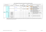
CY8CTST120, CY8CTMG120, CY8CTMA120 September 2008 Silicon Errata for CY8CTST120, CY8CTMG120, and CY8CTMA120 This document describes the errata for the TrueTouch™ devices CY8CTST120, CY8CTMA120, and CY8CTMG120. Details include errata trigger conditions, scope of impact, available workarounds, and silicon revision applicability. Compare this document to the device’s data sheet for a complete functional description. Contact your local Cypress Sales Representative if you have questions. Part Numbers Affected Part Number CY8CTxx120 Ordering Information CY8CTST120-56LFXI CY8CTST120-56LFXIT CY8CTST120-00AXI CY8CTMG120-56LFXI CY8CTMG120-56LFXIT CY8CTMG120-00AXI CY8CTMA120-56LFXI CY8CTMA120-56LFXIT CY8CTMA120-00AXI Errata Summary The following table defines the errata applicability to available CY8CTxx120 family devices. Items [1]. Internal Main Oscillator (IMO) tolerance deviation at temperature extremes [2]. The DP line of the USB interface may pulse low when the PSoC device wakes from sleep, causing an unexpected wakeup of the host computer [3]. Invalid Flash reads may occur if Vdd is pulled to -0.5V just before power on [4]. PMA Index Register fails to auto increment with CPU_Clock set to SysClk/1 (24 MHz) September 25, 2008 Part Number CY8CTxx120 Silicon Revision A CY8CTxx120 A Use workaround. CY8CTxx120 A Use workaround. CY8CTxx120 A Use workaround. Document No. 001-49038 Rev. ** Fix Status Silicon fix is planned. 1 [+] Feedback CY8CTST120, CY8CTMG120, CY8CTMA120 1. Internal Main Oscillator (IMO) tolerance deviation at temperature extremes. PROBLEM DEFINITION Asynchronous digital communication interfaces may fail framing beyond 0 to 70°C. This problem does not affect end product usage between 0 and 70°C. PARAMETERS AFFECTED The IMO frequency tolerance. The worst case deviation when operated below 0°C and above +70°C and within the upper and lower data sheet temperature range is ±5%. TRIGGER CONDITION The asynchronous Rx/Tx clock source IMO frequency tolerance may deviate beyond the data sheet limit of ±4% when operated beyond the temperature range of 0 to +70°C. SCOPE OF IMPACT This problem may affect UART, IrDA, and FSK implementations. WORKAROUND Implement a quartz crystal stabilized clock source on at least one end of the asynchronous digital communications interface. FIX STATUS The cause of this problem and its solution has been identified. Silicon fix is planned to correct the deficiency in silicon. 2. The DP line of the USB interface may pulse low when the PSoC® device wakes from sleep causing an unexpected wakeup of the host computer PROBLEM DEFINITION When the device is operating at 4.75V to 5.25V and the 3.3V regulator is enabled, a short low pulse may be created on the DP signal line during device wakeup. The 15 µs to 20 µs low pulse of the DP line may be interpreted by the host computer as a de-attach or the beginning of a wakeup. PARAMETERS AFFECTED The bandgap reference voltage used by the 3.3V regulator decreases during sleep due to leakage. Upon device wakeup, the bandgap is re-enabled and after a delay for settling, the 3.3V regulator is enabled. On some devices the 3.3V regulator that is used to generate the USB DP signal may be enabled before the bandgap is fully stabilized. This can cause a low pulse on the regulator output and DP signal line until the bandgap stabilizes. In applications where Vdd is 3.3V, the regulator is not used; therefore, the DP low pulse is not generated. WORKAROUND To prevent the DP signal from pulsing low, keep the bandgap enabled during sleep. The most efficient method is to set the No Buzz bit in the OSC_CR0 register. The No Buzz bit keeps the bandgap powered and output stable during sleep. Setting the No Buzz bit results in a nominal 100 µA increase to sleep current. Leaving the analog reference block enabled during sleep also resolves this issue because it forces the bandgap to remain enabled. An example to disable the No Buzz bit is as follows. Assembly M8C_SetBank1 or reg[OSC_CR0], 0x20 M8C_SetBank0 C OSC_CR0 |= 0x20; September 25, 2008 Document No. 001-49038 Rev. ** 2 [+] Feedback CY8CTST120, CY8CTMG120, CY8CTMA120 3. Invalid Flash reads may occur if Vdd is pulled to -0.5V just before power on. PROBLEM DEFINITION When Vdd of the device is pulled below ground just before power on, the first read from each 8K Flash page may be corrupted. This issue does not affect Flash page 0 because it is the selected page upon reset. PARAMETERS AFFECTED When Vdd is pulled below ground before power on, an internal Flash reference may deviate from its nominal voltage. The reference deviation tends to result in the first Flash read from that page returning 0xFF. During the first read from each page, the reference is reset. This results in all future reads returning the correct value. A short delay of 5 µs before the first real read provides time for the reference voltage to stabilize. WORKAROUND To prevent an invalid Flash read, a dummy read from each Flash page must occur before use of the pages. A delay of 5 µs must occur after the dummy read and before a real read. The dummy reads occurs as soon as possible and must be located in Flash page 0 before a read from any other Flash page. An example to read a byte of memory from each Flash page follows. Place it in boot.tpl and boot.asm immediately after the ‘start:’ label. // dummy read from each 8K Flash page // page 1 mov A, 0x20 // MSB mov X, 0x00 // LSB romx // wait at least 5 µs mov X, 14 loop1: dec X jnz loop1 4. PMA Index Register fails to auto increment with CPU_Clock set to SysClk/1 (24 MHz). PROBLEM DEFINITION When the device is operating at 4.75 to 5.25V and the CPU_Clock is set to SysClk/1 (24 MHz), the USB PMA Index Register may fail to increment automatically when used in an OUT endpoint configuration at full speed. When the application program attempts to use the bReadOutEP() function, the first byte in the PMA buffer is always returned. PARAMETERS AFFECTED An internal flip-flop hold problem associated with Index Register increment function. All reads of the associated RAM originate from the first byte. The hold problem has no impact on other circuits or functions within the device. WORKAROUND To make certain that the index register properly increments, set the CPU_Clock to SysClk/2 (12 MHz) during the read of the PMA buffer. An example for the clock adjustment method is listed below. PSoC Designer™ 4.3 User Module Workaround: PSoC Designer Release 4.3 and subsequent releases includes a revised full speed USB User Module, which includes the revised firmware as shown in the following example. ;; ;; 24Mhz read PMA workaround ;; M8C_SetBank1 mov A, reg[OSC_CR0] push A September 25, 2008 Document No. 001-49038 Rev. ** 3 [+] Feedback CY8CTST120, CY8CTMG120, CY8CTMA120 and A, 0xf8 ;clear the clock bits (briefly chg the cpu_clk to 3Mhz) or A, 0x02 ;will set clk to 12Mhz mov reg[OSC_CR0],A ;clk is now set at 12Mhz M8C_SetBank0 .loop: mov mov inc dec jnz A, reg[PMA0_DR] ; Get the data from the PMA space [X], A ; save it in data array X ; increment the pointer [USB_APITemp+1] ; decrement the counter .loop ; wait for count to zero out ;; ;; 24Mhz read PMA workaround (back to previous clock speed) ;; pop A ;recover previous reg[OSC_CR0] value M8C_SetBank1 mov reg[OSC_CR0],A ;clk is now set at previous value M8C_SetBank0 ;; end 24Mhz read PMA workaround References [1] Document # 001-46932 CY8CTST120 TrueTouch™ Single-Touch Touchscreen Controller (Final) [2] Document # 001-46929 CY8CTMG120 TrueTouch™ Multi-Touch Gesture Touchscreen Controller (Final) [3] Document # 001-46901 CY8CTMA120 TrueTouch™ Multi-Touch All-Point Touchscreen Controller (Final) September 25, 2008 Document No. 001-49038 Rev. ** 4 [+] Feedback CY8CTST120, CY8CTMG120, CY8CTMA120 Document History Document Title: Silicon Errata for CY8CTST120, CY8CTMG120, and CY8CTMA120 Document Number: 001-49038 Revision ** ECN 2572224 Submission Date 09/25/08 Orig. of Change KRY Description of Change New errata for Touchscreen device. PSoC is a registered trademark of Cypress Semiconductor Corp. TrueTouch, Programmable System-on-Chip, PSoC Designer, and PSoC Express are trademarks of Cypress Semiconductor Corp. All other trademarks or registered trademarks referenced herein are the property of their respective owners. Cypress Semiconductor 198 Champion Court San Jose, CA 95134-1709 Phone: 408-943-2600 Fax: 408-943-4730 http://www.cypress.com/ © Cypress Semiconductor Corporation, 2008. The information contained herein is subject to change without notice. Cypress Semiconductor Corporation assumes no responsibility for the use of any circuitry other than circuitry embodied in a Cypress product. Nor does it convey or imply any license under patent or other rights. Cypress products are not warranted nor intended to be used for medical, life support, life saving, critical control or safety applications, unless pursuant to an express written agreement with Cypress. Furthermore, Cypress does not authorize its products for use as critical components in life-support systems where a malfunction or failure may reasonably be expected to result in significant injury to the user. The inclusion of Cypress products in life-support systems application implies that the manufacturer assumes all risk of such use and in doing so indemnifies Cypress against all charges. This Source Code (software and/or firmware) is owned by Cypress Semiconductor Corporation (Cypress) and is protected by and subject to worldwide patent protection (United States and foreign), United States copyright laws and international treaty provisions. Cypress hereby grants to licensee a personal, non-exclusive, non-transferable license to copy, use, modify, create derivative works of, and compile the Cypress Source Code and derivative works for the sole purpose of creating custom software and or firmware in support of licensee product to be used only in conjunction with a Cypress integrated circuit as specified in the applicable agreement. Any reproduction, modification, translation, compilation, or representation of this Source Code except as specified above is prohibited without the express written permission of Cypress. Disclaimer: CYPRESS MAKES NO WARRANTY OF ANY KIND, EXPRESS OR IMPLIED, WITH REGARD TO THIS MATERIAL, INCLUDING, BUT NOT LIMITED TO, THE IMPLIED WARRANTIES OF MERCHANTABILITY AND FITNESS FOR A PARTICULAR PURPOSE. Cypress reserves the right to make changes without further notice to the materials described herein. Cypress does not assume any liability arising out of the application or use of any product or circuit described herein. Cypress does not authorize its products for use as critical components in life-support systems where a malfunction or failure may reasonably be expected to result in significant injury to the user. The inclusion of Cypress’ product in a life-support systems application implies that the manufacturer assumes all risk of such use and in doing so indemnifies Cypress against all charges. Use may be limited by and subject to the applicable Cypress software license agreement. September 25, 2008 Document No. 001-49038 Rev. ** 5 [+] Feedback