1
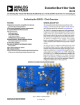
Evaluation Board User Guide
UG-002
One Technology Way • P.O. Box 9106 • Norwood, MA 02062-9106, U.S.A. • Tel: 781.329.4700 • Fax: 781.461.3113 • www.analog.com
Evaluating the AD9551 Multiservice Clock Generator
FEATURES
GENERAL DESCRIPTION
Simple power connection using USB connection and
on-board LDO voltage regulators
LDOs are easily bypassed for power measurements
AC-coupled differential LVPECL SMA connectors
SMA connectors for
2 reference inputs
2 PLL lock detect outputs
Microsoft Windows®–based evaluation software
with simple graphical user interface
On-board PLL loop filter
Easy access to digital I/O and diagnostic signals
via I/O header
Status LEDs for diagnostic signals
USB computer interface
Dip switch configurable for manual operation
Software calculator provides flexibility, allowing programming
almost any rational input/output frequency ratio
This user guide describes the hardware and software of the
AD9551 evaluation board and includes detailed schematics and
PCB layout artwork. The AD9551 Revision D evaluation board
is a compact, easy to use platform for evaluating all features of the
AD9551 multiservice clock generator.
The AD9551 accepts one or two reference input signals to
synthesize one or two output signals. The AD9551 uses a
fractional-N PLL that precisely translates the reference frequency
to the desired output frequency. The input receivers and output
drivers provide both single-ended and differential operation.
Reference conditioning and switchover circuitry internally
synchronizes the two references so that if one reference fails,
there is virtually no phase perturbation at the output.
The AD9551 uses an external crystal and an internal DCXO to
provide for holdover operation. If both references fail, the device
maintains a steady output signal. This may mislead you to believe
that the PLL is locked and the board is configured properly. A
simple test is to move the input REF A or REF B clock a few kilohertz and verify that the changes in output frequency track the input.
08129-001
DIGITAL PICTURE OF THE EVALUATION BOARD
Figure 1. AD9551 Evaluation Board, Revision D
See the last page for an important warning and disclaimers.
Rev. 0 | Page 1 of 12
UG-002
Evaluation Board User Guide
TABLE OF CONTENTS
Features .............................................................................................. 1 Using an SPI Port ..........................................................................5 General Description ......................................................................... 1 Using Dip Switches (Manual Control) .......................................5 Digital Picture of the Evaluation Board ......................................... 1 Using Software to Override Dip Switches (Software Control) ..... 5 Revision History ............................................................................... 2 Software Operation ...........................................................................6 Evaluation Board Hardware ............................................................ 3 Menu Bar of Main Window .........................................................7 Setting up the Power and PC Connections ............................... 3 Button Bar of Main Window .......................................................8 Setting up the Signal Connections ............................................. 3 Using Software to Control the Functional Blocks of AD9551 ...... 8 Bypassing the USB Power Supply ............................................... 3 Using Software to Calculate the Device Settings ................... 10 Evaluation Board Software .............................................................. 4 Routing 26 MHz to Test Port .................................................... 11 Installing the Software ................................................................. 4 Setting the 19.44 MHz Mode .................................................... 12 Using the Software........................................................................ 4 ESD Caution................................................................................ 12 Guide to Programming the AD9551.............................................. 5 REVISION HISTORY
4/09—Revision 0: Initial Version
Rev. 0 | Page 2 of 12
Evaluation Board User Guide
UG-002
EVALUATION BOARD HARDWARE
The following instructions are for setting up the physical
connections to the AD9551 evaluation board.
SETTING UP THE SIGNAL CONNECTIONS
SETTING UP THE POWER AND PC CONNECTIONS
After setting up the power and PC connections, use the
following procedure to set up the signal connections:
Set up the power and PC connections as follows:
1.
1.
Install the AD9551 evaluation software before connecting
the evaluation board to your PC for the first time (see the
Installing the Software section). Administrative privileges
are required for installation.
The AD9551 has the option of either being pin or register
programmable. If the pin programmable option is desired,
then no software is needed to control the part. However, it
is recommended to install the software because if it is not
installed, the computer will recognize the evaluation board
as new hardware and attempt to install drivers.
2.
Connect the USB cables to the evaluation board and the
computer.
By default, the reference inputs on this evaluation board
are ac-coupled and terminated 50 Ω to ground. An
amplitude setting of 6 dBm is sufficient.
2.
To connect a signal to REF B, connect the signal to SMA
Connector J2.
3.
Connect an oscilloscope, spectrum analyzer, or other lab
equipment to any of the J3 to J6 SMA connectors on the
upper right side of the board. The output connectors are
single ended. A 50 Ω termination should be placed on all
unused outputs.
BYPASSING THE USB POWER SUPPLY
The red LED labeled VBUS (CR2) on the AD9551 evaluation
board should illuminate, and the USBSTAT LED should start
blinking. If the USBSTAT LED is not blinking, ensure that
the USB port on the PC is operational and that the USB cable
is not damaged.
3.
Connect a signal generator to REF A SMA Connector J1.
If the Found New Hardware Wizard automatically
appears when the evaluation board is connected, select
Install the software automatically and then click Next.
The evaluation board can be configured to supply power to the
AD9551 from an external power supply. Bypass the USB power
supply as follows:
1.
Remove the F2 ferrite bead (located on the backside of
the board).
2.
Connect a bench power supply to Pin 3.3V_1 of TB1 on
the evaluation board. In addition, resistors on the evaluation
board can be removed to further separate power supply
connections to the AD9551. This is useful for measuring
the AD9551 power consumption. Refer to the evaluation
board schematics provided on the CD in the evaluation board
kit (also available at www.analog.com) for further details.
The Found New Hardware Wizard may appear twice, and
a system restart may be required.
Refer to the Evaluation Board Software section for details on
running the AD9551 evaluation board software.
Rev. 0 | Page 3 of 12
UG-002
Evaluation Board User Guide
EVALUATION BOARD SOFTWARE
The instructions included in this section are for setting up the
AD9551 evaluation board software.
4.
If the evaluation board was not found, a dialog box appears
that allows you to select an evaluation board to use while
the software runs in standalone mode. Standalone mode is
useful for viewing and generating register setup files.
5.
If you connect the evaluation board while the evaluation
board software is running, the window shown in Figure 2
usually appears to prompt you to load the evaluation board
with the evaluation board software settings or to read the
current evaluation board settings into the software.
INSTALLING THE SOFTWARE
Do not connect the evaluation board until the software
installation is complete. To install the software,
1.
Insert the AD9551 evaluation software CD-ROM into a PC
CD disc drive.
2.
Click My Computer, and then double-click the
AD9551EV CD icon.
A window opens showing the contents of the CD divided
into four sections: data sheet, layout, schematic, and software.
The readme.txt file contains a description of the CDROM contents, as well as any last minute instructions or
information.
Double-click the Software folder, and then double-click
AD9551Eval_Setup1.1.0.exe. Follow the installation
instructions. The default location for the evaluation
software is C:\Program Files\Analog Devices\AD9551
Eval Software\.
4.
If there are any updates to the evaluation software on a
supplemental CD or in the \Software\Updates folder, be
sure to copy the new .EXE file, as well as any setup files, to
the default location.
08129-002
3.
Figure 2. SYNC Evaluation Software Window
6.
If the evaluation board was not automatically detected
when it was connected, choose Select Evaluation Board
from the I/O menu, and then select EZSSP-0, EZSSP-1, or
EZSSP-2 (see Figure 3).
USING THE SOFTWARE
1.
Power up and connect the evaluation board to the PC.
2.
Double-click AD9551 Eval Software to run the AD9551
evaluation software.
A hardware installation window appears. Depending on
whether the evaluation board was found by the software, the
text in this window is either light blue, indicating that the
evaluation board was found, or red, indicating that the
evaluation board was not found.
3.
If the evaluation board was found, click in the window
when the Evaluation Software Ready message appears.
The main window of the evaluation board software appears.
Proceed to the Guide to Programming the AD9551 section
for more details about using the software.
Rev. 0 | Page 4 of 12
08129-003
After the evaluation software has been installed, you can run
the software as follows:
Figure 3. Select USB Device Window
Evaluation Board User Guide
UG-002
GUIDE TO PROGRAMMING THE AD9551
The AD9551 can be programmed via an SPI port or by setting
the logic levels on the frequency select pins of the device. To
program the device using the serial port, the evaluation board
software must be installed.
5.
Set the amplitude and frequency. An amplitude setting of
6 dBm is sufficient. Set the frequency to 622.08 MHz.
6.
To connect a signal to REF B, connect the signal to SMA
Connector J2.
For pin programming, there are two options: manually use the
dip switches or use the evaluation board software to override
the settings of the dip switches and change the logic levels of the
frequency select pins. Using the dip switches on the evaluation
board to establish the logic levels on the pins allows the AD9551
to power on with preset conditions. Alternatively, you can use
the software to override the settings of the dip switches on the
evaluation board and change the logic levels on the frequency
select pins.
7.
Connect an oscilloscope, spectrum analyzer, or other lab
equipment to any of the J3 to J6 SMA connectors on the
upper right side of the board.
8.
Power the evaluation board by plugging it into the USB port.
9.
A frequency of 622.08 MHz should be observed on the
OUT1 SMA connector.
If another input and/or output frequency is desired, remove
the USB port. Then change the dip switch settings, and
reapply the USB port connection.
USING AN SPI PORT
After the evaluation software is installed and the evaluation
board is connected to a PC and loaded with the software, the
following procedure can be used to configure and lock the PLLs.
After each dip switch setting, the AD9551 must be powered down
by removing the USB cable to reprogram the AD9551. See the
AD9551 data sheet for an explanation of pin programming.
In this example, the input frequency is 622.08 MHz on REF A,
and the output frequency is 622.08 MHz.
USING SOFTWARE TO OVERRIDE DIP SWITCHES
(SOFTWARE CONTROL)
1.
2.
3.
The evaluation board software can be used to override the
settings of the dip switches and apply a logic level to the
AD9551 frequency selection pins.
Ensure that Jumper JMP3 is positioned for PC control.
Verify that all five jumpers are in place on Connector P2.
Set the S1, S2, and S3 switches high. Set the S4 switch
setting to high, except for RESET, which must be set to low
(RESET is an active high pin).
These steps assume that the input signal is present, that the
evaluation board has not been modified, and that the PLL loop
filter is suitable for the application. However, this guide covers
only simple PLL operation (that is, to start and run the PLL).
For a detailed explanation of more advanced AD9551 features,
see the AD9551 data sheet. In addition, see the Software
Operation section.
USING DIP SWITCHES (MANUAL CONTROL)
After the evaluation software is installed and the evaluation
board is connected to a PC and loaded with the software, the
following steps can be used to configure and lock the PLLs.
In this example, the input frequency is 622.08 MHz on REF A,
and the output frequency is 622.08 MHz.
1.
Ensure that Jumper JMP3 is positioned for PC control.
2.
Verify that all five jumpers are in place on Connector P2.
3.
Set the S1, S2, and S3 dip switch positions to high.
4.
Select 622.08 MHz for the input frequency in the REF A
(MHz) box in the main window of the evaluation software
(see Figure 4 and the Reference Input Boxes section for
more information).
5.
Select 622.08 MHz for the output frequency in the Output
Loop Config: box in the main window of the evaluation
software (see Figure 4).
6.
A frequency of 622.08 MHz should be observed on the
OUT SMA connector.
The following procedure explains how the AD9551 can be programmed manually by using the dip switches on the evaluation
board to set the logic levels of the frequency select pins.
In this example, the input frequency is 622.08 MHz on REF A,
and the output frequency is 622.08 MHz.
1.
Ensure Jumper JMP3 is positioned for manual control.
2.
Verify that all five jumpers are removed on Connector P2.
3.
Set the S1, S2, and S3 dip switch positions to low. (Note
that S2 controls REF B. If REF B is not used, there is no
need to change the S2 settings.).
4.
Connect a signal generator to REF A SMA Connector J1.
By default, the reference inputs on this evaluation board
are ac-coupled and terminated 50 Ω to ground.
These steps assume that the input signal is present, that the
evaluation board has not been modified, and that the PLL loop
filter is suitable for the application. However, these steps are
appropriate only for simple PLL operation (that is, to set up and
run the PLL). See the AD9551 data sheet for more information
about the various AD9551 features.
Rev. 0 | Page 5 of 12
UG-002
Evaluation Board User Guide
SOFTWARE OPERATION
When a subsection window closes after clicking OK, you may
notice that the LOAD button on the main window starts
blinking. This indicates that there are settings that have not
been loaded to the AD9551 evaluation board. Click LOAD to
load these settings to the evaluation board.
08129-004
The main window of the AD9551 evaluation board software is
comprised of subsections that correspond to the major functional
blocks of the AD9551 (see Figure 4). These subsections, most of
which have their own window, are outlined in this section. From
the main window, the window for each functional block can be
accessed by clicking the appropriate box in the main window.
Figure 4. AD9551 Evaluation Software Main Window
Rev. 0 | Page 6 of 12
Evaluation Board User Guide
UG-002
MENU BAR OF MAIN WINDOW
File Menu
The File menu allows you to load a previously saved AD9551
setup file or to save a new AD9551 setup file. A setup file (.STP)
is a text file that contains the AD9551 register setup file, plus
any evaluation board settings.
To load a previously saved setup file, select Load Setup from
the File menu. Note that you must still perform a VCO
calibration. Alternatively, to save a new setup file, select Save
Setup from the File menu.
To exit the evaluation software, select Exit from the File menu.
However, note that no checking is done to ensure that the
existing setup is saved.
Figure 7. Debug Window
The Register Map Debug window, accessed by selecting
Register Debug Window from the View menu, allows you to
write and read registers (see Figure 8).
08129-005
The AD9551 evaluation system allows one PC to control
multiple evaluation boards. The Select USB Device window,
accessed by choosing Select Evaluation Board from the I/O
menu, allows you to select which evaluation board the software
controls (see Figure 5). Click Refresh List to detect a recently
connected evaluation board.
08129-007
I/O Menu
Figure 5. Select USB Device Window
08129-008
Selecting Configure Serial Port from the I/O menu allows you
to control how the USB controller interacts with the AD9551 serial
port (see Figure 6) by configuring Register 0x00 (shown as 00H
in Figure 8).
Figure 8. Register Map Debug Window
08129-006
Help Menu
Selecting Help from the Help menu opens the About AD9551
window, which contains information such as revision number,
region information, and contact information.
Figure 6. Serial Port Configuration Window
View Menu
The Debug window, accessed by selecting Debug Window from
the View menu, allows you to write and read registers directly and
to force the various configuration pins high or low (see Figure 7).
Rev. 0 | Page 7 of 12
UG-002
Evaluation Board User Guide
BUTTON BAR OF MAIN WINDOW
The buttons described in this section provide easy access to
common features.
Load and Save
Clicking Load and Save allows you to load and save an AD9551
setup file. A setup file (.STP) is a text file that contains the AD9551
register setup file, plus any evaluation board settings.
Update
Clicking Update toggles the I/O update bit (Register 0x05, Bit 0) of
the AD9551.
08129-009
Reset
Clicking Reset resets the evaluation board and restores the
AD9551 to its default power-up state. In addition, clicking
Reset enables the VCO calibration function by writing the
enable VCO calibration bit.
Figure 9. REF A List Box (in Main Window)
Reference Dividers
USING SOFTWARE TO CONTROL THE
FUNCTIONAL BLOCKS OF AD9551
The AD9551 evaluation software contains subsections that
correspond to the major functional blocks of the AD9551.
These subsections, most of which have their own window, are
described in this section.
Clicking Click for Details in the REF A Divider and REF B
Divider boxes of the main window accesses the RefA Input
Divider window and the RefB Input Divider window (see
Figure 10 for an example of the RefA Input Divider window).
These windows are used to set the desired reference divider for
the integer or Σ-Δ modulator mode. The counters can be set
individually.
You can access each window by clicking Click for Details in the
appropriate subsection box of the main window.
Most subsection boxes in the main window have a checkbox
labeled SPI. If this box is selected, the software allows serial
port writes when conditions are changed in the corresponding
subsection window.
When a subsection window closes after clicking OK, you may
notice that the LOAD button on the main window starts
blinking. This indicates that there are settings that have not
been loaded to the AD9551 evaluation board. Click LOAD to
load these settings to the evaluation board.
The reference input boxes, which are labeled REF A (MHz) and
REF B (MHz) in the main window, allow you to select an input
frequency for REF A and REF B (see Figure 9 for an example for
REF A). These boxes can be used to change the logic levels of
the input frequency select pins.
Rev. 0 | Page 8 of 12
08129-011
Reference Input Boxes
Figure 10. RefA Input Divider Window
Evaluation Board User Guide
UG-002
PFD and Charge Pump Window
Clicking Click for Details in the DLL box of the main window
accesses the DLL window (see Figure 11). This window can be
used to manually override the automatic time alignment between
the REF A and REF B clock input signals to the PLL1 phase
detector.
Clicking Click for Details in the PFD & Charge Pump box of
the main window accesses the PFD and Charge Pump window
(see Figure 13).
08129-013
DLL Window
08129-015
Figure 11. DLL Window
Input PLL + DCXO Window
Clicking Click for Details in the PLL & DCXO box in the main
window accesses the Input PLL + DCXO window (see Figure 12).
Figure 13. PFD and Charge Pump Window
VCO Control Window
Figure 12. Input PLL + DCXO Window
Rev. 0 | Page 9 of 12
08129-016
08129-014
Clicking Click for Details in the VCO box of the main window
accesses the VCO Control window (see Figure 14).
Figure 14. VCO Control Window
UG-002
Evaluation Board User Guide
OutSel Pin: Box
Clicking Click for Details in the Feedback Divider box of the
main window accesses the Feedback window, which allows you
to change the feedback divider settings (see Figure 15).
The OutSel Pin: drop-down box (see Figure 18) in the main
window controls the logic level on the OUTSEL pin of the
AD9551. However, this value can be overwritten by using the
SPI control register.
08129-019
Feedback Window
Figure 18. OutSel Pin Box (in Main Window)
USING SOFTWARE TO CALCULATE THE DEVICE
SETTINGS
The following procedure explains how the evaluation board
software can be used to automatically calculate and set the
settings to program the AD9551.
08129-017
In this example, the input frequency is 122.88 MHz on REF A,
and the output frequency is 122.88 MHz.
Figure 15. Feedback Window
1.
Ensure that Jumper JMP3 is positioned for PC control.
2.
Verify that all five jumpers are in place on Connector P2.
3.
Set the positions of the S1, S2, and S3 dip switches to high.
4.
Click Calculate Device Settings in the main window of the
evaluation board software.
P0, P1, and P2 (Output Dividers) Boxes
08129-020
Selecting the SPI check box in any of the divider settings boxes
(that is, the P0, P1, or P2 box) in the main window enables a
drop-down selection of predetermined divider settings (see
Figure 16).
Figure 19. Calculate Device Settings Button (in Main Window)
The Enable Control? window, shown in Figure 20,
appears.
08129-018
5.
Figure 16. P0, P1, and P2 Boxes (in Main Window)
Output Loop Config: Box
08129-029
08129-021
The Output Loop Config: box can be used to change the output
frequency of the AD9551. This control changes the logic levels
of the output frequency selection pins of the AD9551.
Figure 20. AD9551 Serial Port Programming Warning
Figure 17. Output Loop Config: Box (in Main Window)
6.
Rev. 0 | Page 10 of 12
Click Yes to enable serial port register programming.
Evaluation Board User Guide
The Calculator window, shown in Figure 21, appears.
5.
The Enable Control? window, shown in Figure 23,
appears.
08129-024
7.
UG-002
Figure 23. AD9551 Serial Port Programming Warning
Click Yes to enable serial port register programming.
7.
The Calculator window, shown in Figure 24, appears.
08129-022
6.
Figure 21. Calculator Window
8.
Type 122.88 into the Ref A Base Frequency: box and
122.88 into the Output 1 Base Frequency: box.
9.
Click Calculate Settings, and then click Apply Settings.
You should now be able to measure 122.88 MHz at the
OUT1 SMA connector.
ROUTING 26 MHz TO TEST PORT
The following procedure explains how to route the 26 MHz
crystal oscillator to the AD9551 test port. The test port is SMA
J7 and is labeled output PLL locked.
1.
Ensure that Jumper JMP3 is positioned for PC control.
2.
Verify that all five jumpers are in place on Connector P2.
3.
Set the positions of the S1, S2, and S3 dip switches to high.
4.
Click Calculate Device Settings in the main window of the
evaluation board software.
08129-025
In this example, the input frequency is 122.88 MHz on REF A,
and the output frequency is 122.88 MHz.
Figure 24. Calculator Window
8.
Type 122.88 into the Ref A Base Frequency: box and
122.88 into the Output 1 Base Frequency: box.
9.
Click Calculate Settings, and then click Apply Settings.
You should now be able to measure 122.88 MHz at the
OUT1 SMA connector.
08129-023
10. From the View menu in the main window, select Register
Debug Window. The window shown in Figure 25 appears.
Figure 22. Calculate Device Settings Button (in Main Window)
Rev. 0 | Page 11 of 12
Evaluation Board User Guide
08129-027
08129-026
UG-002
Figure 25. Register Debug Window
Figure 26. Input PLL + DCXO Window
11. Bit 3 of Register 0x17 must be set to 1 to enable the PLL
locked pin as a test port. By default, the 26 MHz crystal
frequency is present at the output.
12. The ac signal has a dc offset of approximately 1.6 V. Be
aware that some test equipment has a limit of 0 V dc;
therefore, a dc block must be used in such cases.
SETTING THE 19.44 MHz MODE
08129-028
The following instructions can be used to configure the
AD9551 to operate in the 19.44 MHz mode. Refer to the
AD9551 data sheet for more details about this mode of
operation.
The following case is an example for the AD9551 in
19.44 MHz mode:
Figure 27. PFD and Charge Pump Window
1.
Replace the crystal on the evaluation board.
2.
Replace the loop filter capacitor on the evaluation board.
3.
Click Click for Details in the PLL & DCXO box in the
main window of the evaluation board software to access
the Input PLL + DCXO window (see Figure 26).
4.
Select 19.44MHz Mode in the Input PLL Mode: box, and
then click OK.
5.
Click Click for Details in the PFD & Charge Pump box in
the main window of the evaluation board software to
access the PFD and Charge Pump window (see Figure 27).
6.
Change the charge pump current to the appropriate
current level specified in the AD9551 data sheet
(approximately 25 μA), and then click OK.
7.
If the LOAD button in the main window starts blinking,
this indicates that there are settings that have not been
loaded to the AD9551 evaluation board. Click LOAD to
load these settings to the evaluation board.
ESD CAUTION
Evaluation boards are only intended for device evaluation and not for production purposes. Evaluation boards are supplied “as is” and without warranties of any kind, express,
implied, or statutory including, but not limited to, any implied warranty of merchantability or fitness for a particular purpose. No license is granted by implication or otherwise under
any patents or other intellectual property by application or use of evaluation boards. Information furnished by Analog Devices is believed to be accurate and reliable. However, no
responsibility is assumed by Analog Devices for its use, nor for any infringements of patents or other rights of third parties that may result from its use. Analog Devices reserves the
right to change devices or specifications at any time without notice. Trademarks and registered trademarks are the property of their respective owners. Evaluation boards are not
authorized to be used in life support devices or systems.
©2009 Analog Devices, Inc. All rights reserved. Trademarks and
registered trademarks are the property of their respective owners.
UG08129-0-4/09(0)
Rev. 0 | Page 12 of 12