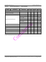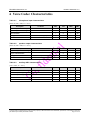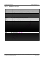
1
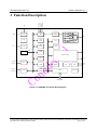
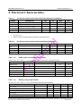
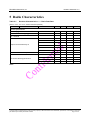
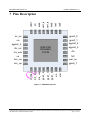
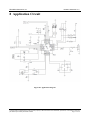
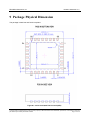
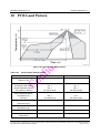
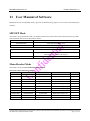
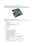
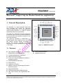
RDA5869 Data Sheet Bluetooth® Single-Chip for Headset/hand-free applications sw avdd uart_rx uart_tx dvdd led1 led0 29 28 27 26 25 24 gpio0_0 vio 2 23 gpio0_1 22 agpio0_6 21 agpio0_5 3 i2c_scl 4 i2c_sda 5 va GND PAD RDA5869 32 PIN 13 15 16 gpio1_0 xin xtal gpio0_7 14 mic_vip 17 gpio1_1 pwr_on 8 12 mic_vin gpio1_2 NC 18 10 19 7 11 6 mic_vop rfio mic_von 20 9 This single-chip RDA5869 is implemented in a standard digital 55nm CMOS process technology and requires minimal external components to provide total solutions especially for headset applications. The chip is packaged as 32- pin, 4 mm × 4 mm QFN. 31 1 agpio2_2 The radio part of RDA5869 has been designed to provide low power, low cost, and robust applications for communications in the globally available 2.4 GHz unlicensed ISM band. 30 ac_on micbias The RDA5869 is a highly-integrated mixed-signal SOC integrated with 2.4GHz RF transceiver compliant with Bluetooth core 2.1 and ARM7-based microprocessor baseband. It is ideal for wireless headset/hand-free device applications vbatt 1 General Description 32 Rev.1.3–10.2012 Figure 1-1. RDA5869 Top View 1.1 Features Fully integrated CMOS radio and ARM7-based Friendly UART/I2C interface baseband with on-chip ROM and RAM Integrated charger circuit Compliant with Bluetooth 2.1 specification internal LDO and DC-DC buck on-chip voice codec with differential microphone in and speaker out ports Supporting 26MHz DCXO /TCXO Internal 32k LPO. Low power consumption Extremely small size chip package with minimum external components Supports for EEPROM Integrated internal programmable 8K-bit efuse LED control interface with programmable flash mode Copyright © RDA Microelectronics Inc. 2011. All rights are reserved. The information contained herein is the exclusive property of RDA and shall not be distributed, reproduced, or disclosed in whole or in part without prior written permission of RDA. RDA Microelectronics, Inc. RDA5873 Datasheet V1.3 1.2 Applications RDA5869 is tailored for the mono-headset bluetooth earphone applications. The information contained herein is the exclusive property of RDA and shall not be distributed, reproduced, or disclosed in whole or in part without prior written permission of RDA. Page 2 of 20 RDA Microelectronics, Inc. RDA5873 Datasheet V1.3 2 Table of Contents 1 General Description .................................................................................................................................... 1 1.1 Features ............................................................................................................................................... 1 1.2 Applications ........................................................................................................................................ 2 2 Table of Contents......................................................................................................................................... 2 3 Function Description................................................................................................................................... 3 3.1 Radio ................................................................................................................................................... 4 3.2 Auxiliary features ............................................................................................................................... 4 3.3 Baseband ............................................................................................................................................. 4 3.4 Voice codec .......................................................................................................................................... 4 3.5 Interface .............................................................................................................................................. 4 3.6 Bluetooth Stack................................................................................................................................... 4 3.7 Microprocessor Unit .......................................................................................................................... 5 3.8 EEPROM Interface............................................................................................................................ 5 3.9 LED and PWM ................................................................................................................................... 5 4 Electrical Characteristics ........................................................................................................................... 6 5 Radio Characteristics.................................................................................................................................. 8 6 Voice Codec Characteristics ..................................................................................................................... 10 7 Pins Description......................................................................................................................................... 11 8 Application Circuit.................................................................................................................................... 13 9 Package Physical Dimension .................................................................................................................... 14 10 PCB Land Pattern ..................................................................................................................................... 15 11 User Manual of Software .......................................................................................................................... 17 12 Change List ................................................................................................................................................ 18 13 Contact Information ................................................................................................................................. 19 The information contained herein is the exclusive property of RDA and shall not be distributed, reproduced, or disclosed in whole or in Page 2 of 20 part without prior written permission of RDA. RDA Microelectronics, Inc. RDA5873 Datasheet V1.3 3 Function Description A A Φ 256K ROM SCU POR 32K RAM SPI2 RF BT_RF PLL P PWR_ON LDO x x N Modem G BB DC/DC G PCM_CLK PCM_DOUT PCM_DIN PCM_SYNC SW VBAT D Envelon AHB ARM7 TRAP MIC_VIN VOICE CODEC VIC MIC_OUT I2C_SDA I2C_SCL I2C TIMER DMA UART_TX UART_RX UART APB BRIDGE PLL OSC XTAL XIN APB GPIO 32K/LPO GPIO ports Figure 3-1. RDA5869 Functional Block Diagram The information contained herein is the exclusive property of RDA and shall not be distributed, reproduced, or disclosed in whole or in Page 3 of 20 part without prior written permission of RDA. RDA Microelectronics, Inc. RDA5873 Datasheet V1.3 3.1 Radio ♦ ♦ ♦ ♦ ♦ ♦ Build-in TX/RX switch and on-chip balun Fully integrated frequency synthesizer without any external component Support DCXO or external reference clock direct input Programmable output power control meets Class 2 or Class 3 requirements High performance in receiver sensitivity Integrated channel-select filter 3.2 Auxiliary features ♦ ♦ ♦ On-chip low-dropout regulator to support battery power supply directly High power efficiency integrated DC-DC buck On-chip software controlled power management 3.3 Baseband ♦ ♦ Internal RAM allows fully-speed data transfer, mixed voice and data, and fully piconet operation Logic for forward error correction, header error control, access code correlation, CRC, demodulation , encryption bit stream generation, whitening and transmit pulse shaping ♦ ♦ Support eSCO and AFH Support up to Bluetooth v2.1 3.4 Voice codec ♦ Support A-law, μ-law and CVSD digitized audio CODEC in PCM interface ♦ ♦ Differential microphone analog input ports Differential analog speaker output ports 3.5 Interface ♦ ♦ ♦ ♦ Provides UART HCI interface, up-to 4Mbps Provides I2C interface for host to do configuration Provides PCM audio interface Provides 3-wire and 2-wire WIFI co-existence handshake interface 3.6 Bluetooth Stack ♦ Compliant with Bluetooth 2.1 specification The information contained herein is the exclusive property of RDA and shall not be distributed, reproduced, or disclosed in whole or in Page 4 of 20 part without prior written permission of RDA. RDA Microelectronics, Inc. ♦ RDA5873 Datasheet V1.3 Bluetooth HID profile version 1.0 compliant 3.7 Microprocessor Unit The RDA5869 microprocessor unit executes software from the link control (LC) layer up to the application layer components that ensure adherence to the Bluetooth Human Interface Device (HID) profile. The microprocessor is based on an ARM7, 32-bit RISC processor with embedded ICE-RT debug and JTAG interface units. There is 256 KB of ROM for program storage and boot-up, 32 KB of RAM for scratch-pad data, and patch RAM code. The internal boot ROM provides power-on reset flexibility, which enables the same device to be used in different HID applications with an external serial EEPROM. At power-up, the lowest layer of the protocol stack is executed from the internal ROM memory. External patches may be applied to the ROM-based firmware to provide flexibility for bug fixes and feature additions. The device can also support the integration of user applications. 3.8 EEPROM Interface The EEPROM can contain customer application configuration information including: application code, configuration data, patches, pairing information, BD_ADDR, baud rate, and so on. Native support for the Microchip® 24LC128, Microchip 24AA128, and ST Micro® M24128-BR is included. 3.9 LED and PWM The rda5869 has 2 internal LEDs and PWM. The PWM module consists of the following: ♦ LED 0-1 and PWM ♦ Each of the two LED and PWM channels contains the following registers: – 16-bit initial value register (read/write) – 16-bit toggle register (read/write) The information contained herein is the exclusive property of RDA and shall not be distributed, reproduced, or disclosed in whole or in Page 5 of 20 part without prior written permission of RDA. RDA Microelectronics, Inc. RDA5873 Datasheet V1.3 4 Electrical Characteristics Table 4-1 DC Electrical Specification (Recommended Operation Conditions): SYMBOL DESCRIPTION MIN TYP MAX UNIT VBAT Supply Voltage from battery or LDO 3.5 4.0 4.2 V Tamb Ambient Temperature -20 27 +50 ℃ VIL CMOS Low Level Input Voltage 0 0.3*VIO V VIH CMOS High Level Input Voltage 0.7*VIO VIO V VTH CMOS Threshold Voltage 0.5*VIO V Notes: 1. VIO=2.8~3.3V 2. Battery minimum storage voltage=2V (typical, normal temperature). Table 4-2 DC Electrical Specification (Absolute Maximum Ratings): SYMBOL DESCRIPTION MIN TYP MAX UNIT Tamb Ambient Temperature -20 +60 °C IIN Input Current -10 +10 mA VIN Input Voltage -0.3 VIO+0.3 V Vlna LNA Input Level +5 dBm Table 4-3 DCDC Power consumption specification (VBAT = 4.0 V, VIO = 2.8V, TA = +27℃, RF 3.3dBm, DCDC mode unless otherwise specified) STATE DESCRIPTION Condition Headset voice Headset SNIFF 500ms cycle NO INQUIRE and PAGE SCAN HCI only active Both SCAN 1.28S cycle INQUIRE and PAGE SCAN DeepSleep internal LDO off Table 4-4 LDO_ON off TYP UNIT 22 mA 0.8 mA 4.2 mA 0.75 mA 250 µA 25 µA Battery Charger specification (AC_ON = 5 V, VIO = 2.8V, TA = +27℃,LDO off mode unless otherwise specified) STATE Condition Input voltage Trickle Charging mode current Constant current charging mode current Float voltage Sleep mode current MIN TYP MAX UNIT 4.5 5 6 V Vbatt < 3V 52 mA 3V < Vbatt < 4.2V 126 mA 4.2 V 6 uA The information contained herein is the exclusive property of RDA and shall not be distributed, reproduced, or disclosed in whole or in Page 6 of 20 part without prior written permission of RDA. RDA Microelectronics, Inc. Table 4-5 RDA5873 Datasheet V1.3 Efuse specification ( VIO = 5V, TA = +27℃, writing mode unless otherwise specified) STATE Condition MIN TYP MAX UNIT Efuse writing voltage range 3.5 4 5 V Read mode VIO voltage 2.7 3 3.3 V The information contained herein is the exclusive property of RDA and shall not be distributed, reproduced, or disclosed in whole or in Page 7 of 20 part without prior written permission of RDA. RDA Microelectronics, Inc. RDA5873 Datasheet V1.3 5 Radio Characteristics Table 5-1 Receiver Characteristics ------ Basic Data Rate (VBAT = 4.0 V, TA = 27°C, unless otherwise specified) SYMBOL PARAMETER CONDITIONS MIN TYP MAX UNIT Sensitivity @0.1% BER -87 -82 / dBm Maximum received [email protected]% BER 10 / / dBm / +10 / dB F=F0 + 1MHz / -20 / dB F=F0 - 1MHz / -15 / dB F=F0 + 2MHz / -35 / dB F=F0 - 2MHz / -35 / dB F=F0 + 3 MHz / -35 / dB F=F0 - 3MHz / -36 / dB F=Fimage / / 0 dB 30MHz–2000MHz -15 / / dBm 2000MHz–2400MHz -25 / / dBm 2500MHz–3000MHz -25 / / dBm 3000MHz–12.5GHz -15 / / dBm General specifications C/I c-channel Adjacent channel selectivity C/I Adjacent channel selectivity C/I Out-of-band blocking performance Notes: The information contained herein is the exclusive property of RDA and shall not be distributed, reproduced, or disclosed in whole or in Page 8 of 20 part without prior written permission of RDA. RDA Microelectronics, Inc. Table 5-2 RDA5873 Datasheet V1.3 Transmit Characteristics ------ Basic Data Rate (VBAT = 4.0V, TA = 27 °C, unless otherwise specified) SYMBOL PARAMETER CONDITIONS MIN TYP MAX UNIT / 3.3 5 dBm 10 / / dB / 0.9 / MHz F=F0 + 1MHz / -20 / dBm F=F0 - 1MHz / -20 / dBm F=F0 + 2MHz / -40 / dBm F=F0 - 2MHz / -40 / dBm F=F0 + 3MHz / -48 / dBm F=F0 - 3MHz / -48 / dBm F=F0 + >3MHz / -50 / dBm F=F0 - >3MHz / -50 / dBm △f1avg Maximum modulation 141 156 164 kHz △f2max Minimum modulation / 141 / kHz △f2avg/△f1avg / 0.9 / / ICFT / -1 / kHz -1.4 0.9 +1.2 kHz/50us Drift (1 slot packet) / 4 / kHz Drift (5 slot packet) / 4.4 / kHz General specifications Maximum RF transmit power RF power control range 20dB band width Adjacent channel transmit power Drift rate Notes: 1. power control range could be tuned for 20dB. The information contained herein is the exclusive property of RDA and shall not be distributed, reproduced, or disclosed in whole or in Page 9 of 20 part without prior written permission of RDA. RDA Microelectronics, Inc. RDA5873 Datasheet V1.3 6 Voice Codec Characteristics Table 6-1 microphone input characteristics (VA=2.7V, VIO = 2.8V, TA = +27℃) Description MIN TYP MAX UNIT Input voltage scale at max gain / 6 / mV Input voltage scale at min gain / 300 / mV Gain resolution / 2 / dB / 60 / dB / 2.8 / kHz Condition MIN TYP MAX UNIT Load=32ohm, 0.1THD / 0.64 1.8 Vpp THD@1kHz Condition Gain=0dB,300mVpp input Bandwidth Table 6-2 speaker output characteristics (VA=2.7V, VIO = 2.8V, TA = +27℃) Description Output voltage full scale swing Output -3dB bandwidth THD@1kHz 2 full scale output = 1.8Vpp / Gain resolution Table 6-3 60 kHz / 2 dB dB auxiliary ADC characteristics ( VIO = 2.8V, TA = +27℃) Description Condition MIN TYP MAX UNIT resolution / 8 / bits Minimum input voltage / 20 50 mV Maximum input voltage / / 1.5 V LSB / 5 / mV bandwidth / 10 / kHz The information contained herein is the exclusive property of RDA and shall not be distributed, reproduced, or disclosed in whole or in Page 10 of 20 part without prior written permission of RDA. RDA Microelectronics, Inc. RDA5873 Datasheet V1.3 vbatt sw avdd uart_rx uart_tx dvdd led1 led0 32 31 30 29 28 27 26 25 7 Pins Description ac_on 1 24 gpio0_0 vio 2 23 gpio0_1 agpio2_2 3 22 agpio0_6 i2c_scl 4 21 agpio0_5 i2c_sda 5 va GND PAD RDA5869 32 PIN 16 xtal micbias 15 gpio0_7 xin 17 14 8 gpio1_0 mic_vip 13 pwr_on gpio1_1 18 12 7 gpio1_2 mic_vin 11 NC mic_vop 19 10 6 mic_von rfio 9 20 Figure 7-1. RDA5869 Top View The information contained herein is the exclusive property of RDA and shall not be distributed, reproduced, or disclosed in whole or in Page 11 of 20 part without prior written permission of RDA. RDA Microelectronics, Inc. Table 7-1 PIN RDA5873 Datasheet V1.3 RDA5869 Pins Description NO. DESCRIPTION AC_ON VIO AGPIO2_2 I2C_SCL I2C_SDA VA MIC_VIN MIC_VIP MICBIAS MIC_VON MIC_VOP GPIO1_2 GPIO1_1 GPIO1_0 XIN XTAL GPIO0_7 PWR_ON 1 2 3 4 5 6 7 8 9 10 11 12 13 14 15 16 17 18 Charger DC voltage supply (5V) External decouple capacitor port or power supply for ext IO (3V) Programmable analog/digital general purpose I/O port I2C interface Clock signal I2C interface Data signal External decouple capacitor port for codec voltage supply Negative analog input from the microphone Positive analog input from the microphone Voltage output for codec external components Negative analog output to the speaker Positive analog output to the speaker Programmable digital general purpose I/O port. PCM_CLK Programmable digital general purpose I/O port. PCM_SYNC Programmable digital general purpose I/O port. PCM_DIN 26Mhz crystal input or external clock input 26Mhz crystal input Programmable digital general purpose I/O port. PCM_DOUT Power on enable(effective 3V) NC 19 Non-connected RFIO AGPIO0_5 AGPIO0_6 GPIO0_1 GPIO0_0 LED0 20 21 22 23 24 25 Bluetooth RF signal I/O port Programmable analog/digital general purpose I/O port Programmable analog/digital general purpose I/O port Programmable digital general purpose I/O port Programmable digital general purpose I/O port LED 0 control LED1 26 LED 1 control DVDD 27 Decouple Capacitor (1.2V) UART_TX 28 UART data output UART_RX AVDD SW VBAT 29 30 31 32 UART data input IO power supply (1.8V) Internal DC/DC switch voltage output Battery power supply The information contained herein is the exclusive property of RDA and shall not be distributed, reproduced, or disclosed in whole or in Page 12 of 20 part without prior written permission of RDA. RDA Microelectronics, Inc. RDA5873 Datasheet V1.3 8 Application Circuit Figure 8-1 Application diagram The information contained herein is the exclusive property of RDA and shall not be distributed, reproduced, or disclosed in whole or in Page 13 of 20 part without prior written permission of RDA. RDA Microelectronics, Inc. RDA5873 Datasheet V1.3 9 Package Physical Dimension The package is lead-free and RoHS-compliant. Figure9-1. 32-Pin 4x4 Quad Flat No-Lead (QFN) The information contained herein is the exclusive property of RDA and shall not be distributed, reproduced, or disclosed in whole or in Page 14 of 20 part without prior written permission of RDA. RDA Microelectronics, Inc. RDA5873 Datasheet V1.3 10 PCB Land Pattern Figure 10-1.Classification Reflow Profile Table 10-1 Classification Reflow Profiles Profile Feature Sn-Pb Eutectic Assembly Pb-Free Assembly Average Ramp-Up Rate 3 ℃/second max. 3 ℃/second max. -Temperature Min (Tsmin) 100 ℃ 150 ℃ -Temperature Max (Tsmax) 100 ℃ 200 ℃ -Time (tsmin to tsmax) 60-120 seconds 60-180 seconds -Temperature (TL) 183 ℃ 217℃ -Time (tL) 60-150seconds 60-150 seconds Peak /Classification See Table 9-2 See Table 9-3 10-30 seconds 20-40 seconds Ramp-Down Rate 6 ℃/second max. 6 ℃/seconds max. Time 25 oC to Peak 6 minutes max. 8 minutes max. (TSmax to Tp) Preheat Time maintained above: Temperature(Tp) Time within 5 oC of actual Peak Temperature (tp) Temperature The information contained herein is the exclusive property of RDA and shall not be distributed, reproduced, or disclosed in whole or in Page 15 of 20 part without prior written permission of RDA. RDA Microelectronics, Inc. RDA5873 Datasheet V1.3 Table 10-2 Pb-free Process – Package Peak Reflow Temperatures Package Thickness Volume mm3 <350 Volume mm3 ≥350 <2.5mm 240 + 0/-5 ℃ 225 + 0/-5 ℃ ≥2.5mm 225 + 0/-5 ℃ 225 + 0/-5 ℃ Table 10-3 Pb-free Process – Package Classification Reflow Temperatures Package Volume mm3 Volume mm3 Volume mm3 Thickness 350-2000 <350 >2000 <1.6mm 260 + 0 ℃ * 260 + 0 ℃ * 260 + 0 ℃ * 1.6mm – 2.5mm 260 + 0 ℃ * 250 + 0 ℃ * 245 + 0 ℃ * ≥2.5mm 250 + 0 ℃ * 245 + 0 ℃ * 245 + 0 ℃ * *Tolerance : The device manufacturer/supplier shall assure process compatibility up to and including the stated classification temperature(this mean Peak reflow temperature + 0 ℃. For example 260+ 0 ℃ ) at the rated MSL Level. Note 1: All temperature refer topside of the package. Measured on the package body surface. Note 2: The profiling tolerance is + 0 ℃, - X ℃ (based on machine variation capability)whatever is required to control the profile process but at no time will it exceed – 5 ℃. The producer assures process compatibility at the peak reflow profile temperatures defined in Table 13-3. Note 3: Package volume excludes external terminals(balls, bumps, lands, leads) and/or non integral heat sinks. Note 4: The maximum component temperature reached during reflow depends on package the thickness and volume. The use of convection reflow processes reduces the thermal gradients between packages. However, thermal gradients due to differences in thermal mass of SMD package may sill exist. Note 5: Components intended for use in a “lead-free” assembly process shall be evaluated using the “lead free” classification temperatures and profiles defined in Table13-1, 13-2, 13-3 whether or not lead free. RoHS Compliant The product does not contain lead, mercury, cadmium, hexavalent chromium, polybrominated biphenyls (PBB) or polybrominated biphenyl ethers (PBDE), and are therefore considered RoHS compliant. ESD Sensitivity Integrated circuits are ESD sensitive and can be damaged by static electricity. Proper ESD techniques should be used when handling these devices. The information contained herein is the exclusive property of RDA and shall not be distributed, reproduced, or disclosed in whole or in Page 16 of 20 part without prior written permission of RDA. RDA Microelectronics, Inc. RDA5873 Datasheet V1.3 11 User Manual of Software RDA5869 has two incompatible modes / protocol for different using propose. And it can be controlled by the software. SPP/OPP Mode This mode is using for transfer data, user defined command or protocol and some similar proposes by UART. The commands and events of this mode as follow: Command DATA Start SPP Profile 0x01 0x01 0xFE 0x01 0x10 Send Data 0x01 0x02 0xFE (Data Length (One byte)) Data Event DATA Receive Connection 0x04 0xFF 0x08 0x60 (State: 0x01 for connection 0x00 for disconnection) (Address (Six bytes)) Receive Data 0x04 0xFF (Data Length + 1 (One byte)) 0x61 Data Mono-Headset Mode This mode is using for mono-headset Bluetooth earphone. The function, statue and action as follow: FUNCTION STATUE ACTION LED SPEAKER Power On Power off Long Press Power 3s Blue Flush 1s One Long Pair Power off Long Press Power 6s Blue Red Long Flush One Short Pair Success Power On Power off Power On Unconnected Power On Red Flush 1s (Cyc. 11s) Connected Power On Blue Flush 1s (Cyc. 11s) Low Power Power On Red Flush 1s (Cyc. 2s) Auto Power off Power On Unconnected 15min Active A Call Receive A Call Press Power Release A Call Active Call Press Power Reject A Call Receive A Call Long Press Power 3s Blue Flush 2s Long Press Power 5s Blue Flush 2s One Long Blue Flush 1s (Cyc. 3s) The information contained herein is the exclusive property of RDA and shall not be distributed, reproduced, or disclosed in whole or in Page 17 of 20 part without prior written permission of RDA. RDA Microelectronics, Inc. RDA5873 Datasheet V1.3 12 Change List REV DATE AUTHER CHANGE DESCRIPTION V1.0 1/18/2012 Xu Donglin Initial version. V1.1 5/16/2012 Xie Zichen Add user manual V1.2 9/10/2012 Xu Donglin Update the parameters. V1.3 10/29/2012 Yang Guanghui Define multi-function port The information contained herein is the exclusive property of RDA and shall not be distributed, reproduced, or disclosed in whole or in Page 18 of 20 part without prior written permission of RDA. RDA Microelectronics, Inc. RDA5873 Datasheet V1.3 13 Contact Information RDA Microelectronics, Inc. Suite 601 Building 4, 690 Bibo Road Pudong District, Shanghai Tel: 86-21-50271108 Fax: 86-21-50271099 Postal Code: 201203 Suite 1108 Block A, e-Wing Center, 113 Zhichun Road Haidian District, Beijing Tel: 86-10-62635360 Fax: 86-10-82612663 Postal Code: 100086 2501 Room, District A, XiNian Center, 6021 ShenNan Road, Nanshan District, Shenzhen. Tel: 86-755- 86187018 Fax: 86-755- 33395366 Postal Code: 518057 The information contained herein is the exclusive property of RDA and shall not be distributed, reproduced, or disclosed in whole or in Page 19 of 20 part without prior written permission of RDA.