1
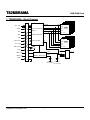
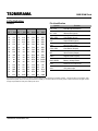
TS2MSRAMA
2MB SRAM Card
Description
Features
The TS2MSRAMA is a 2MB PCMCIA SRAM memory IC
•
Compatible with PCMCIA Rel. 2.0 SRAM Card.
card with 16pcs of 128Kx8 static RAM and one piece of
•
Main Memory : 2048K words x 8 bit or
1024K words x 16 bit.
2Kx8 EEPROM assembled on the printed circuit board.
The SRAM card is compatible with PCMCIA release 2.0.
•
Attribute Memory : 2Kx8 EEPROM.
•
Supply Voltage :
Placement
Single Power Supply : 5V + 10%
•
E
F G
E
Memory Backup Voltage :
Main Battery : CR2025 Replaceable battery
E
for data retention.
Sub-Battery : Installed battery for data retention
while changing the main battery.
D
D
(It can not be replaced.)
Connector
•
Recommended operating temperature : 0 - 70 C.
Durability : Testing to 10000 cycles.
Dimensions
A
2 MB
SRAM CARD
B
Lock
1
2
Protected
3
1
Battery Stand
2
Battery Lock Switch
3
Write-Protect Switch
Transcend Information Inc.
•
C
Side
Millimeters
Inches
A
85.60 + 0.200
3.37 + 0.008
B
54.00 + 0.100
2.126 + 0.004
C
3.30 + 0.050
0.130 + 0.002
D
11.00 + 0.300
0.433 + 0.012
E
1.00 + 0.050
0.039 + 0.002
F
2.45 + 0.050
0.097 + 0.002
G
0.85 + 0.050
0.034 + 0.002
TS2MSRAMA
2MB SRAM Card
1. TS2MSRAMA-- Block Diagram
D0-D15
8
D0 - D15
D0 - D7
/WE
/REG
Data Transceiver
/CE0-/CE15
/Buffer
A0-A16
/WE
/OE
/CE1,/CE2
A0 - A20
/CD1,/CD2
68 Pins Connector
WP
/CE
17
A0 - A16
8
Bus Controller
/CE
17
VCC
D0 - D7
/WE
SRAM
/OE
128Kx8
/CE
A0 - A16
Vbat2
/BVD1
Reset
/BVD2
Battery Back-up IC
Vbat1
/OE
/WE
GND
1st Battery 2nd Battery
(Replaceable) (Rechargeable)
128Kx8
Address Decoder
VCC
Transcend Information Inc.
SRAM
/OE
TS2MSRAMA
2MB SRAM Card
2. Pin Definition
Pinouts
Pin Identification
Symbol
Pin
Pin
Pin
Pin
Pin
Pin
Pin
Pin
No. Name No. Name No. Name No. Name
01
GND
18
RFU
35
GND
52
RFU
02
D3
19
A16
36
/CD1
53
RFU
03
D4
20
A15
37
D11
54
RFU
04
D5
21
A12
38
D12
55
RFU
05
D6
22
A7
39
D13
56
RFU
06
D7
23
A6
40
D14
57
RFU
07
/CE1
24
A5
41
D15
58
RFU
08
A10
25
A4
42
/CE2
59
RFU
09
/OE
26
A3
43
RFU
60
RFU
10
A11
27
A2
44
RFU
61
/REG
11
A9
28
A1
45
RFU
62
BVD2
12
A8
29
A0
46
A17
63
BVD1
13
A13
30
D0
47
A18
64
D8
14
A14
31
D1
48
A19
65
D9
15
/WE
32
D2
49
A20
66
D10
16
RFU
33
WP
50
RFU
67
/CD2
17
VCC
34
GND
51
VCC
68
GND
Function
D0 ~ D15
Data Bus (Bi-directional)
A0 ~ A20
Address Bus (Input)
/CE1,/CE2
Card Enable (Input)
/OE
Output Enable (Input)
/WE
Write Enable (Input)
/CD1,/CD2
Card Detect (Output)
WP
Write Protect (Output)
/REG
Register Select (Input)
BVD1,BVD2
Battery Voltage Detect
RFU
Reserved for Future Use
VCC
+5V power input
This technical information is based on industry standard data and tests believed to be reliable. However , Transcend makes no warranties, either
expressed or implied, as to its accuracy and assumes no liability in connection with the use of this product. Transcend reserves the right to make
changes in specifications at any time without prior notice.
Transcend Information Inc.