1
Processor Configuration Registers
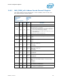
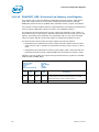
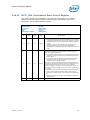
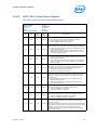
2.5.22
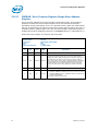
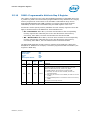
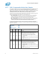
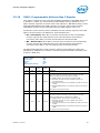
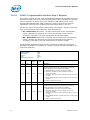
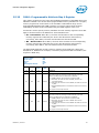
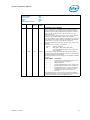
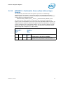
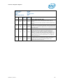
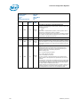
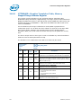
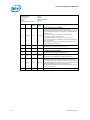
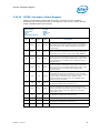
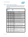
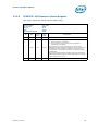
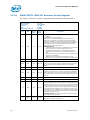
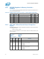
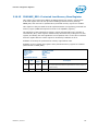
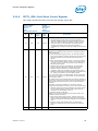
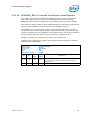
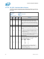
PAM6—Programmable Attribute Map 6 Register
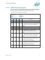
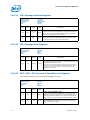
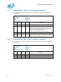
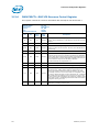
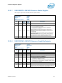
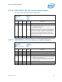
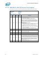
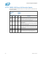
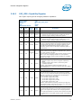
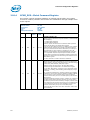
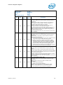
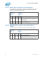
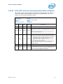
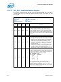
This register controls the read, write and shadowing attributes of the BIOS range from
E_8000h to E_FFFFh. The Uncore allows programmable memory attributes on 13
legacy memory segments of various sizes in the 768 KB to 1 MB address range. Seven
Programmable Attribute Map (PAM) registers are used to support these features.
Cacheability of these areas is controlled using the MTRR register in the core.
Two bits are used to specify memory attributes for each memory segment. These bits
apply to host accesses to the PAM areas. These attributes are:
• RE – Read Enable. When RE=1, the host read accesses to the corresponding
memory segment are claimed by the Uncore and directed to main memory.
Conversely, when RE=0, the host read accesses are directed to DMI.
• WE – Write Enable. When WE=1, the host write accesses to the corresponding
memory segment are claimed by the Uncore and directed to main memory.
Conversely, when WE=0, the host read accesses are directed to DMI.
The RE and WE attributes permit a memory segment to be Read Only, Write Only,
Read/Write or Disabled. For example, if a memory segment has RE=1 and WE=0, the
segment is Read Only.
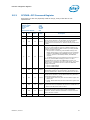
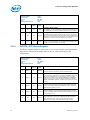
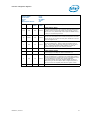
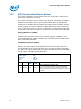
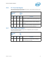
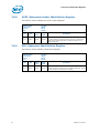
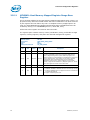
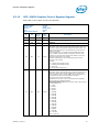
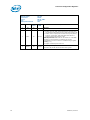
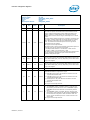
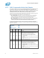
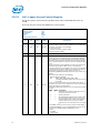
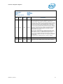
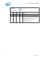
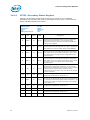
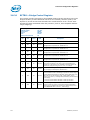
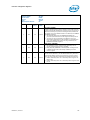
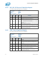
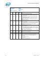
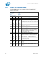
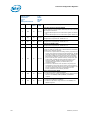
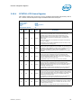
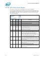
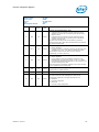
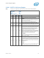
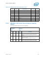
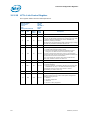
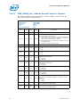
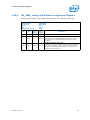
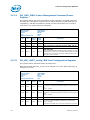
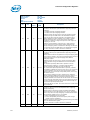
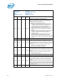
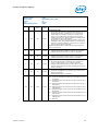
B/D/F/Type:
Address Offset:
Reset Value:
Access:
Size:
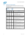
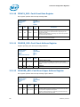
BIOS Optimal Default
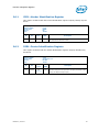
Bit
Attr
Reset
Value
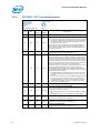
7:6
RO
0h
5:4
RW
00b
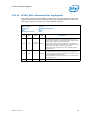
3:2
RO
0h
1:0
Datasheet, Volume 2
0/0/0/PCI
86h
00h
RW
8 bits
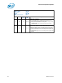
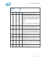
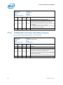
0h
RW
00b
RST/
PWR
Description
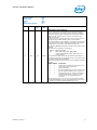
Reserved
Uncore
0EC000–0EFFFF Attribute (HIENABLE)
This field controls the steering of read and write cycles that
address the BIOS area from 0EC000h to 0EFFFFh.
00 = DRAM Disabled. All accesses are directed to DMI.
01 = Read Only. All reads are sent to DRAM, all writes are
forwarded to DMI.
10 = Write Only. All writes are sent to DRAM, all reads are serviced
by DMI.
11 = Normal DRAM Operation. All reads and writes are serviced by
DRAM.
This register is locked by Intel TXT.
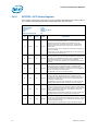
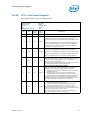
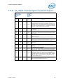
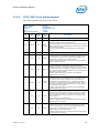
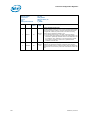
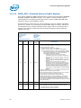
Reserved
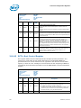
Uncore
0E8000–0EBFFF Attribute (LOENABLE)
This field controls the steering of read and write cycles that
address the BIOS area from 0E8000h to 0EBFFFh.
00 = DRAM Disabled. All accesses are directed to DMI.
01 = Read Only. All reads are sent to DRAM. All writes are
forwarded to DMI.
10 = Write Only. All writes are sent to DRAM. All reads are serviced
by DMI.
11 = Normal DRAM Operation. All reads and writes are serviced by
DRAM.
This register is locked by Intel TXT.
69