1
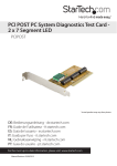
PC REPAIR
PCI POST Diagnostics Test Card
PCIPOST
Instruction Guide
* Actual product may vary from photo
Revised: December 5, 2002
The Professionals’ Source For Hard-to-Find Computer Parts
17
FCC COMPLIANCE STATEMENT
Technical Support
This equipment has been tested and found to comply with the limits for a Class B
digital device, pursuant to part 15 of the FCC Rules. These limits are designed to
provide reasonable protection against harmful interference in a residential installation.
This equipment generates, uses and can radiate radio frequency energy and, if not
installed and used in accordance with the instructions, may cause harmful interference
to radio communications. However, there is no guarantee that interference will not
occur in a particular installation. If this equipment does cause harmful interference to
radio or television reception, which can be determined by turning the equipment off
and on, the user is encouraged to try to correct the interference by one or more of the
following measures:
The following technical resources are available for this StarTech.com product:
• Reorient or relocate the receiving antenna.
• Increase the separation between the equipment and receiver.
• Connect the equipment into an outlet on a circuit different from that to which the
receiver is connected.
• Consult the dealer or an experienced radio/TV technician for help.
On-line help:
We are constantly adding new information to the Tech Support section of our web site. To
access this page, click the Tech support link on our homepage, www.startech.com. In the
tech support section there are a number of options that can provide assistance with this
card.
Knowledge Base - This tool allows you to search for answers to common issues using
key words that describe the product and your issue.
FAQ - This tool provides quick answers to the top questions asked by our customers.
Downloads - This selection takes you to our driver download page where you can
find the latest drivers for this product.
Call StarTech.com tech support for help: 1-519-455-4931
Support hours: Monday to Friday 9:00AM to 5:00PM EST (except holidays)
Warranty Information
This product is backed by a lifetime warranty. In addition StarTech.com warrants its
products against defects in materials and workmanship for the periods noted below,
following the initial date of purchase. During this period, the products may be
returned for repair, or replacement with equivalent products at our discretion. The
warranty covers parts and labor costs only. StarTech.com does not warrant its products
from defects or damages arising from misuse, abuse, alteration, or normal wear and
tear.
Limitation of Liability
In no event shall the liability to StarTech.com Ltd. (or its officers, directors, employees or
agents) for any damages (whether direct or indirect, special, punitive incidental,
consequential, or otherwise), loss of profits, loss of business, or any pecuniary loss,
arising out of related to the use of the product exceed the actual price paid for
the product.
Some states do not allow the exclusion or limitation of incidental or consequential
damages. If such laws apply, the limitations or exclusions contained in this statement
may not apply to you.
1
16
Table of Contents
9C
9E
A0
A2
A4
A8
AA
AC
AE
B2
B4
B6
B8
BC
BE
BF
C0
D0
D2
D4
D6
D8
DA
DC
Setup power management.
Enable hardware interrupts.
Set time of day.
Check key lock.
Initialize typematic rate.
Ease F2 prompt.
Scan for F2 stroke.
Enter SETUP.
Clear in-POST flag.
POST done - prepare to boot operating system.
One beep.
Check password (option).
Clear global descriptor table.
Clear parity checkers.
Clear screen (option).
Clear virus and backup remainders.
Try to boot with INT 19.
Interrupt handler error.
Unknown interrupt error.
Pending interrupt error.
Initialize option ROM error.
Shutdown error.
Extended BLOCK move.
Shutdown 10 error.
The following are for boot block in Flash ROM
POST Code
E2
E3
E4
E5
E6
E7
E8
E9
EA
EB
EC
ED
EE
Pheonix POST Routine Description
Initialize the chipset.
Initialize refresh counter.
Check for forced Flash.
Check H/W status ROM.
BIOS ROM is OK.
Do a complete RAM test.
Do OEM initialization.
Initialize interrupt controller.
Read in the bootstrap code.
Initialize all vectors.
Boot the Flash program.
Initialize the boot device.
Boot code was read OK.
Introduction . . . . . . . . . . . . . . . . . . . . . . . . . . . . . . . . . . . . . . . . . . . . . . . . . . . . . . . . 2
Installation . . . . . . . . . . . . . . . . . . . . . . . . . . . . . . . . . . . . . . . . . . . . . . . . . . . . . . . . . 3
Using Your Card . . . . . . . . . . . . . . . . . . . . . . . . . . . . . . . . . . . . . . . . . . . . . . . . . . . . 3
Quick Error Reference Table . . . . . . . . . . . . . . . . . . . . . . . . . . . . . . . . . . . . . . . . . . 4
AMI Bios . . . . . . . . . . . . . . . . . . . . . . . . . . . . . . . . . . . . . . . . . . . . . . . . . . . . . . . . . . 5
Award BIOS . . . . . . . . . . . . . . . . . . . . . . . . . . . . . . . . . . . . . . . . . . . . . . . . . . . . . . . 12
Phoenix BIOS . . . . . . . . . . . . . . . . . . . . . . . . . . . . . . . . . . . . . . . . . . . . . . . . . . . . . 14
2
Introduction
Thank you for purchasing a StarTech.com PCI Power-On Self Test (POST) diagnostic
card. Now you can save hours of troubleshooting time by simply plugging the card into
an open PCI slot on a malfunctioning PC and booting up the computer. The PCIPOST
will scan the system and report the problem in the form of a code that you can crossreference to the error chart in this manual. PC technicians and system builders can
quickly pinpoint the problem and avoid replacing non-defective parts.
Features
• Fits into any open PCI slot
• Lists generic errors for AMI BIOS, PHOENIX BIOS, and AWARD BIOS
• Error codes clearly visible through on-board LEDs
• Backed by StarTech.com’s lifetime warranty
Before You Begin
To ensure a quick and easy card installation, please read through this section carefully
before attempting to install the card.
WARNING! PCI cards, like all computer equipment, can be severely damaged by static
electricity. Be sure that you are properly grounded before opening your computer case or
touching your PCI card. StarTech.com recommends that you wear an anti-static strap
when installing any computer component. If an anti-static strap is unavailable, discharge
yourself of any static electricity build-up by touching a large grounded metal surface
(such as the computer case) for several seconds. Also be careful to handle the PCI card
by its edges and not the gold connectors.
Contents
This package should contain:
• 1 x PCIPOST diagnostic card
• 1 x Error code listing (included in manual)
NOTE: Before you begin the test, make sure that you know the BIOS supplier and BIOS
version. Without this information, you will not be able to determine the meaning of the
error code. The PCIPOST card does not generate the error codes, the codes are
generated by the BIOS supplier and are specific to that BIOS. Contact your
motherboard manufacturer if you encounter any difficulties. The PCIPOST is
compatible with every IBM-compatible system, but since there are numerous BIOS
versions and suppliers, you may not find your system BIOS information in the error
code listing. This information may be available in your motherboard manufacturer’s
user guide. Your BIOS manufacturer can likely supply you with this information if you
contact them.
15
49
4A
4C
4E
50
51
52
54
56
58
5A
5C
60
62
64
66
68
6A
6C
6E
70
72
74
76
7C
7E
80
82
84
86
88
8A
8C
90
91
92
93
94
96
98
9A
Initialize PCI BUS and devices.
Initialize all video adapters in system.
Shadow video BIOS ROM.
Display copyright notice.
Display CPU type and speed.
Initialize EISA board.
Test keyboard.
Set key click if enabled.
Enable keyboard.
Test for unexpected interrupts.
Display prompt "Press F2 to enter setup".
Test RAM between 512 to 640K.
Test extended memory.
Test extended memory lines.
Jump to UserPatch1.
Configure advanced cache registers.
Enable external and CPU cache.
Display external cache size.
Display shadow message.
Display non-disposable segments.
Display error messages.
Check for configuration errors.
Test real-time clock.
Check for keyboard error.
Setup hardware interrupt vectors.
Test coprocessor if present.
Disable onboard I/O ports.
Detect and install external RS-232 ports.
Detect and install external parallel ports.
Reinitialize onboard I/O ports.
Initialize BIOS data area.
Initialize extended BIOS data area.
Initialize floppy controller.
Initialize hard disk controller.
Initialize local BUS hard disk controller.
Jump to UserPatch2
Built MPTABLE for multi-processor boards.
Disable A20 address line.
Clear huge ES segment register.
Search for option ROMs.
Shadow option ROMs.
3
14
Pheonix BIOS POST Test Code Listing
POST Code
02
04
06
08
09
0A
0C
0E
0F
10
11
12
14
16
18
1A
20
22
24
26
2A
2C
2E
32
34
35
37
38
39
3A
3C
3D
40
42
44
46
47
48
Pheonix POST Routine Description
Verify real mode.
Get CPU type.
Initialize system hardware.
Initialize chipset register with initial POST value.
Set in POST flag.
Initialize CPU register.
Initialize cache to initial POST values.
Initialize I/O CPU register.
Initialize the local BUS IDE.
Initialize power management.
Load alternate registers with initial POST values.
Jump to UserPatch0.
Initialize keyboard control.
BIOS ROM checksum.
5254 timer initialization.
8237 DMA controller initialization.
Test DRAM refresh.
Test 8042 keyboard controller.
Set ES segment register to 4 GB.
Autosize DRAM.
Clear 512K base RAM.
Teat 512K base address line.
Test 512K base memory.
Test CPU BUS-clock frequency.
Test CMOS RAM.
Initialize alternate chipset registers.
Reinitialize the chipset.
Shadow system BIOS RAM.
Reinitialize the cache.
Autosize cache.
Configure advanced chipset registers.
Load alternate registers with CMOS values.
Set initial CPU speed.
Initialize interrupt vectors.
Initialize BIOS interrupts.
Check ROM copyright notice.
Initialize manager for PCI option ROMs.
Check video configuration against CMOS.
Installation
This section will guide you through the installation of your PCI card and the related
software. Please read through the instructions carefully and complete each step in the
order listed.
Installing the Card
1. Make sure that your system is unplugged and you are grounded.
2. Remove the cover of your system (see your computer's user manual for details, if
necessary) and gently turn your computer onto its side.
3. Locate an empty PCI slot (usually white in colour) that can provide a clear view of
the LEDs on the card and remove the metal plate that covers the rear bracket. You
may need a Phillips screwdriver to perform this step. Hang on to the screw! You will
need it to secure the card later.
4. Gently insert the card into the empty slot, making sure it is firmly seated and that
you are able to see the LEDs on the card.
5. Secure the card in place using the screw you removed in Step 3.
6. When you are ready to begin the test, plug your system in and turn it on.
Using Your Card
When power is first supplied to your computer, the power supply will generate a power
good signal that is received by the motherboard clock if all the output voltages from the
power supply are correct. When the clock receives this signal, it stops forcing a reset
signal to the CPU and the CPU begins processing instructions. These initial tasks are
monitored by the circular green D1+ and D2+ LEDs. If the top D1+ LED does not light,
there is a problem with the reset. If the D2+ LED does not light, there is a problem with
the system clock.
The BIOS will then initialize, verify, and test numerous functions in your computer.
Every initialization, verification, and test is its own separate program with its own error
code. As the BIOS scrolls through these processes, you will see these error codes flashing
across the LEDs. If an initialization, verification, or test fails, the system will pause and
the error code will remain on the LED. You can now consult the error code listing and
determine where the problem lies.
The error codes on the card are based on hex (0, 1, 2 ... 9, A, B, C, D, E, F, 10, 11, 12 ... 19,
1A, 1B, 1C, 1D, 1E, 1F, 20 ...) as opposed to decimal arithmetic. Therefore, a range of
“2C ~ 34” means “2C, 2D, 2E, 2F, 30, 31, 32, 33, 34”.
13
4
QUICK ERROR REFERENCE TABLE
Error
caused
by
AMI
BIOS
(c) 1990
HiFLEX
BIOS
AMI
Award Phoenix Quadtel
BIOS
AT
(c) 1994
BIOS
WinBIOS
Troubleshooting
CPU
01~02
01~02
01~02
01
02~04
Replace CPU (speed
should be the same)
Math
9C~9D
Compressor
9C~9D
45
3E
76~78
1. Replace CPU
2. Replace CPU if
NPU is built in CPU
Memory
13
20~24
D1~D3
20
40~58
C1
08
31~32
09~1F
1C~20
28~2C
32, 3A
60~68
1. Check and clean
RAM module
2. Replace RAM
module
Display
Card
2C~34
2C~34
0D~0E
2B~33
46
1. Check and clean
display card slot
and golden finger
2. Replace Display
card
M/B error
Others
DIY
Code
Others
DIY
Code
Others
DIY
Code
Others
DIY
Code
Others
DIY
Code
Call customer
service center for
help or replace M/B
3E
BF
40
41
42
43
4E
4F
50
51
52
53
60
61
62
63
B0
B1
E1-EF
FF
Setup cache controller.
Chipset initialization (program chipset registers with setup values)
Display virus protest disabled or enabled.
Initialize floppy drive and controller.
Initialize hard drive and controller.
Detect and initialize the serial, parallel and game ports.
Check manufacture POST loop.
Security check.
Write CMOS (write all CMOS values back tp RAM and clear screen).
Pre-boot enabled (enable parity check, NMI and cache).
Initialize option ROMs (address range from 0C800H to 0EFFFFH).
Initialize time value in 40h; BIOS area.
Setup virus protection according to setup.
Set system speed for boot.
Setup NumLock status according to setup.
Boot attempt (set low stack, and boot via INT 19H).
Spurious (if interrupt occurs in protected mode).
Unclaimed NMI (if NMI occurs, press F1 to disable NMI, F2 for reboot).
Setup pages (E1 - page 1, E2 - page 2, ... etc).
Boot the operating system.
5
12
AWARD BIOS POST Test Code Listing
POST Code
C0
01
02
03
04
05
07
BE
C1
C5
C6
08
09
0A
0B
0C
0D
0E
0F
10
11
14
15
16
17
18
19
1A
1F
20
21-2F
30
31
32
3C
3D
Award POST Routine Description
Turn off chipset cache.
Test processor flag register.
Test all processor registers except SS, SP and BP with pattern FF and 00.
Initialize Chips (RTC, 8254, 8237, 8259), reset math coprocessor, clear
CMOS shutdown byte and page register.
Test DRAM refresh.
Black video, and keyboard controller initialization.
Test CMOS interface and battery status.
Initialize chipset with power on BIOS defaults.
Memory presence test (OEM specific test to size on-board memory)
Early shadow (OEM specific-early shadow enabled for fast boot).
Cache presence test (external cache size detection).
Setup low memory (base 64K memory test).
TEST CMOS RAM checksum, load default value is test is bad.
Setup interrupt vector table.
Test CMOS RAM checksum and load default value if test is bad.
Initialize keyboard (detect keyboard type and set NUM_LOCK status).
Initialize and detect video adapter interface.
Test video memory, write sign-on message to screen.
Set up shadow RAM - Enable shadow according to setup.
Test DMA controller 0.
Test DMA controller 1.
Test DMA page registers (74612).
Test Timer 0 counter 2
Test 8259-1 interrupt mask register (port 21H)
Test 82592 interrupt mask register (port A1H)
Test stuck 8259’s interrupt bits.
Test 8259 interrupt functionality.
Test stuck NMI bits (verify NMI can be cleared).
Display CPU clock.
Set EISA mode.
Enable Slot 0 (initialize slot 0 - system board)
Enable Slot 1-15 (initialize slot 1 to 15)
Size base memory and extended memory.
Test base memory and extended memory.
Test EISA extended memory. Skip in ISA mode.
Setup enabled.
Initialize and setup mouse.
AMI BIOS POST Test Codes
AMI WinBIOS/HiFLEX 101094
POST Code
AMI WinBIOS uncompress code checkpoints description
C2
NMI is Disabled. Power on delay starting.
C5
Power on delay complete. Going to disable cache, is any.
C6
Calculating ROM BIOS checksum.
C7
ROM BIOS checksum passed. CMOS shutdown register test
to be done next.
C8
CMOS shutdown register test done. CMOS checksum calculation
to be done next.
CA
CMOS checksum calculation is done, CMOS Diag byte written.
CMOS status register about to initialization for Date and Time.
CB
CMOS status register initialization done.
Any initialization before keyboard BAT is to be done next.
CD
BAT command to keyboard controller is to be issued.
CE
Keyboard controller BAT result verified.
Any initialization after KB controller BAT is to be done next.
CF
Initialization after KB controller BAT done.
Keyboard command byte is to be written next.
D1
Keyboard controller command byte is written.
Going to check pressing of <INS> key during power-on.
D2
Check for pressing of <INS> key during power-on done.
Going to disable DMA and Interrupt controllers.
D3
DMA controller #1, #2, interrupt controller #1, #2 disabled.
Chipset initialization/auto memory detection about to begin.
D4
Chipset initialization/auto memory detection over.
To uncompress the RUNTIME code.
D5
RUNTIME code is uncompressed.
D0
Transfer control to uncompressed code in shadow ram at F000:FFF0
6
11
Runtime code is uncompressed in F000 shadow ram
The system BIOS gives control to various BUSes at the following checkpoints to do
various tasks on different BUSes.
POST Code
AMI HiFLES BIOS/WinBIOS runtime code description
01
Processor register test about to start and NMI to be disabled.
POST Code
AMI HiFLEX BIOS/WinBIOS Checkpoints of the BUSes
02
NMI is disabled. Power-on delay starting.
2A
Different BUSes initialization to start if present.
03
Power on delay complete. To check soft reset/power-on.
38
Different BUSes initialization to start if present.
05
Soft reset/power-on determined. Going to disable cache if any.
39
Display different BUSes initialization error message.
06
POST code to be uncompressed.
95
Initialization of different BUSes optional ROMs from C800 to start.
07
POST code is uncompressed. CPU initialization and CPU data area
initialization is to be done next.
08
CPU and CPU data area initialization is done. CMOS checksum
calculation is to be done next.
09
CMOS checksum calculation is done, CMOS Diag byte written.
CMOS initialization is to begin.
0A
CMOS initialization done (if any).
CMOS status about to initialize for Data and Time.
0B
CMOS status register initialization done.
Any initialization before keyboard BAT is to be done next.
HIGH BYTE XY
0C
KB controller I/B free. Going to issue the BAT command to the
keyboard controller.
0D
BAT command to keyboard controller is issued.
Going to verify the BAT command.
0E
Keyboard controller BAT result verified.
Any initialization before keyboard BAT is to be done next.
0F
Initialization after KB controller BAT done.
Keyboard command byte to be written next.
10
Keyboard controller command byte is written.
Going to issue pin 23, 24 blocking/unblocking command.
The upper nibble ‘X’ indicates the function #is being executed. ‘X’ can be from 0 to 7.
0=func#0, disable all devices on the BUS concerned.
1=func#1, static devices initialized on the BUS concerned.
2=func#2, output devices initialized on the BUS concerned.
3=func#3, input device initialized on the BUS concerned.
4=func#4, IPL device initialized on the BUS concerned.
5=func#5, general device initialized on the BUS concerned
6=func#6, error reporting for the BUS concerned.
7=func#7, add-on ROM initialized for all BUSes.
11
Pin 23, 24 of keyboard controller is blocked/unblocked.
Going to check pressing of <INS> key during power-on.
12
Checking for pressing of <INS> key during power-on done.
Going to disable DMA and Interrupt controllers.
13
DMA controller #1, #2, interrupt controller #1, #2 disabled.
Video display is disabled and port B is initialized. Chip set
initialization about to begin.
While control is inside the different BUS routine, additional checkpoints are outputted to
port 80h as WORD to identify the routines under execution. These are WORD
checkpoints: the LOW BYTE of the checkpoint is the system BIOS checkpoint from
where the control is passed to the different BUD routines and the HIGH BYTE of the
checkpoint is the identification of which the routine is being executed in the different
BUSes. The details of HIGH BYTE of these checkpoints are as follows:
The lower nibble ‘Y’ indicates the BUS on which the different routines are being
executed. ‘Y’ can be from 0 to 5.
0=Generic DIM (Device Initialization Manager).
1=On-board system devices.
2= ISA devices.
3=EISA devices.
4=ISA PnP devices.
5=PCI devices.
7
10
96
Going to do any initialization before C800 optional ROM control.
15
Chipset initialization over. 8254 timer test about to start.
97
Any initialization before C800 optional ROM control is over.
Optional ROM check and control will be done next.
19
8254 timer test over. About to start memory refresh test.
98
Optional ROM control is done. About to give control to do any
required processing after optional ROM returns control.
1A
Memory refresh line is toggling. Going to check 15 micro second
ON/OFF time.
Any initialization required after optional ROM test over.
Going to setup timer data area and printer base address.
20
99
Memory refresh period 30 micro second test complete. Base 64K
memory initialized.
9A
Return after setting timer and printer base address.
Going to set the RS-232 base address.
23
Base 64K memory initialized. Going to set BIOS stack and to do
any setup before interrupt vector initialization.
9B
Returned RS-232 base address.
Going to do any initialization before coprocessor test.
24
Setup required before interrupt vector initialization is complete.
Interrupt vector initialization is about to begin.
Required initialization before coprocessor is over.
Going to initialize the coprocessor next.
25
9C
Interrupt vector initialization is done. Going to read input port of
8042 for turbo switch and to clear password if post diag switch is on.
Coprocessor initialized. Going to do any initialization after
coprocessor test.
26
9D
Input port of 8042 is read. Going to initialize global data for
turbo switch.
Initialization after coprocessor test is complete.
Going to check extended keyboard, keyboard ID and num-lock.
27
9E
Global data initialization for turbo switch is over.
Any initialization before setting video mode is to be done next.
9F
Extended keyboard check is done, ID flag set, and num-lock on/off.
Keyboard ID command to be issued.
28
Initialization before setting video mode is complete,
Going for monochrome mode and colour mode setting.
Keyboard ID command issued. Keyboard ID flag reset.
2A
Different BUSes initialization to start if present.
A0
Keyboard ID flag reset. Cache memory test to follow.
2B
A1
About to give control for any setup required before optional video
ROM check.
A2
Cache memory test over. Going to display any soft errors.
2C
A3
Soft error display complete. Going to set keyboard typematic rate.
Processing before video ROM control is done.
About to look for optional video ROM and give control.
A4
Keyboard typematic rate set. To program memory wait states.
2D
A5
Memory wait states programming over.
Going to clear the screen and enable parity/NMI.
Optional video ROM control is done.
About to give control to do any processing after video ROM
returns control.
NMI and parity enabled.
Going to do any initialization required before giving control to
optional ROM at E000.
2E
A7
Return from processing after the video ROM control.
If EGA/VGA not found the do display memory R/W test.
2F
EGA/VGA not found. Display memory R/W test about to begin.
A8
Initialization before E000 ROM control over. E000 ROM to get
control next.
30
Display memory R/W test passed.
About to look for the retrace checking.
A9
Returned from E000 ROM control.
Going to do any initialization required after E000 optional ROM control.
31
Display memory R/W test or retrace checking failed.
About to alternate Display memory R/W test.
AA
Initialization after E000 optional ROM control is over.
Going to display the system configuration.
32
Alternate Display memory R/W test passed.
About to look for the alternate display retrace checking.
B0
System configuration is displayed.
34
Video display checking over. Display mode to be set next.
A1
Going to copy any code to specific area.
37
Display mode set. Going to display the power-on message.
00
Copying of code to specific area done. Going to give control to INT-19
boot loader.
38
Different BUSes initialization to start if present.
39
Display different BUSes initialization error messages.
3A
New cursor position read and saved. Going to display Hit
<DEL> message.
9
8
59
Hit <DEL> message cleared. <WAIT...> message displayed.
About to start DMA and interrupt controller test.
60
DMA page register test passed. To do DMA#1 base register test.
62
DMA#1 base register test passed. To do DMA#2 base register test.
65
DMA#2 base register test passed. To program DMA unit 1 and 2.
66
DMA unit 1 and 2 programming over. To initialize 8259
interrupt controller.
67
8259 initialization over.
7F
Extended NMI sources enabling is in progress.
80
Keyboard test started. Clearing output buffer and checking for stuck key.
About to issue keyboard reset command.
81
Keyboard reset error/stuck key found.
About to issue keyboard controller interface test command.
82
Keyboard controller interface test over.
About to write command byte and initialize circular buffer.
83
Command byte written. Global data initialization done. About to check
for lock key.
84
Lock key checking over. About to check for memory size mismatch
with CMOS.
85
Memory size check done.
About to display soft error and check or password or bypass setup.
Memory above 1M cleared. Going to save memory size.
86
Password checked. About to do programming before setup.
4E
Memory test started. About to display the first 64K memory size.
87
4F
Memory size display started. This will be updated during memory test.
Going for sequential and random memory test.
Programming before setup complete.
Going to uncompress SETUP code and execute CMOS setup.
88
50
Memory testing/initialization below 1M complete.
Going to adjust display memory size for relocation/shadow.
Returned from CMOS setup program and screen is cleared.
About to do programming after setup.
89
51
Memory size display adjusted due to relocation/shadow.
Memory test above 1M to follow.
Programming after setup complete. Going to display power on
screen message.
8B
52
Memory testing/initialization above 1M complete.
Going to save memory size information.
First screen message displayed. <WAIT...> message displayed.
About to do Video BIOS shadow.
8C
53
Memory size information is saved. CPU registers are saved.
Going to enter in real mode.
Video BIOS shadow successful.
Setup options programming after CMOS setup about to start.
8D
Setup options are programmed. Mouse check and initialization is next.
54
Shutdown successful, CPU in real mode.
Going to disable gate A20 line and disable parity/NMI.
8E
Mouse check and initialization complete. Going for hard disk
controller reset.
57
A20 address line, parity/NMI disable successful.
Going to adjust memory size depending on relocation/shadow.
8F
Hard disk controller reset done. Floppy setup to be done next.
58
Memory size adjusted for relocation/shadow. Going to clear.
Hit <DEL> message.
91
Floppy setup complete. Hard disk setup to be done next.
94
Hard disk setup complete. To set base and extended memory size.
95
Memory size adjusted due to mouse support. Initialization of
different BUSes and optional ROMs from C800 to start.
3B
Hit <DEL> message displayed. Virtual mode memory test about to start.
40
Going to prepare the descriptor tables.
42
Descriptor tables prepared. Going to enter in Virtual mode for
memory test.
43
Entered in the virtual mode. Going to enable interrupts for
diagnostics mode.
44
Interrupts enabled (if diagnostics switch is on).
Going to initialize data to check memory wrap around at 0:0.
45
Data initialized. Going to check for memory wrap around at 0:0 and
finding the total system memory size.
46
Memory wrap around test done. Memory size calculation over.
About to go for writing patterns to test memory.
47
Pattern to be tested and written in extended memory.
Going to write patterns in base 640K memory.
48
Pattern written in base memory.
Going to find out amount of memory below 1M memory.
49
Amount of memory below 1M found and verified.
Going to find out amount of memory above 1M.
4B
Amount of memory above 1M found and verified. Check for soft reset
and going to clear memory below 1M for soft reset.
4C
Memory below 1M cleared. Going to clear memory above 1M.
4D