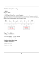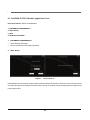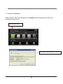
1
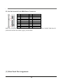
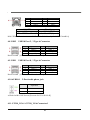
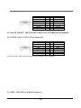
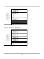
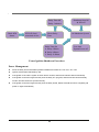
VBOX-3100
In-Vehicle Computing
User's Manual
Version 1.1
Document Name VBOX-3100 User Manual
Document No. UM2012310010
1.1
Version
Date
Oct 24, 2012
Reversion History :
Reversion
Date
From
To
1.0
Feb 17, 2012
Initial document issued
Stanley Chou
1.0
GPIO & Delay Time Setting
Stanley Chou
1.1
Oct 24, 2012
Notes
1
Author(s)
SINTRONES® Technology Corp.
User Manual
Copyright
©2009 by SINTRONES® Technology Corp. All Rights Reserved.
No part of this publication may be reproduced, transcribed, stored in a retrieval system,
translated into any language, or transmitted in any form or by any means such as electronic,
mechanical, magnetic, optical, chemical, photocopy, manual, or otherwise, without prior written
permission from SINTRONES® Technology Corp.
Other brands and product names used herein are for identification purposes only and may be
trademarks of their respective owners.
Disclaimer
SINTRONES® Technology Corp. shall not be liable for any incidental or consequential
damages resulting from the performance or use of this product.
SINTRONES® Technology Corp. makes no representation or warranty regarding the content of
this manual. Information in this manual had been carefully checked for accuracy;however, no
guarantee is given as to the correctness of the contents. For continuing product improvement,
SINTRONES® Technology Corp. reserves the right to revise the manual or make changes to
the specifications of this product at any time without notice and obligation to any person or
entity regarding such change. The information contained in this manual is provided for general
use by customers.
This device complies to Part 15 of the FCC Rules. Operation is subject to the following two
conditions:
1. This device may not cause harmful interference.
2. This device must withstand any background interference including those that may
cause undesired operation.
2
Safety Information
Read the following precautions before setting up a SINTRONES Product.
Electrical safety
• To prevent electrical shock hazard, disconnect the power cable from the electrical
outlet before relocating the system.
• When adding or removing devices to or from the system, ensure that the power
cables for the devices are unplugged before the signal cables are connected.
If possible, disconnect all power cables from the existing system before you add a
device.
• Before connecting or removing signal cables from the motherboard, ensure that all
power cables are unplugged.
• Seek professional assistance before using an adapter or extension cord.
These devices could interrupt the grounding circuit.
• Make sure that your power supply is set to the correct voltage in your area.
If you are not sure about the voltage of the electrical outlet you are using, contact
your local power company.
• If the power supply is broken, do not try to fix it by yourself. Contact a qualified
service technician or your retailer.
Operation safety
• Before installing the motherboard and adding devices on it, carefully read all the
manuals that came with the package.
• Before using the product, make sure all cables are correctly connected and the
power cables are not damaged. If you detect any damage, contact your dealer
immediately.
• To avoid short circuits, keep paper clips, screws, and staples away from connectors,
slots, sockets and circuitry.
• Avoid dust, humidity, and temperature extremes. Do not place the product in any
area where it may become wet.
• Place the product on a stable surface.
• If you encounter technical problems with the product, contact a qualified service
technician or your retailer.
CAUTION
Incorrectly replacing the battery may damage this computer. Replace only with the same or its
equivalent as recommended by SINTRONES® Technology Corp. Dispose used battery
according to the manufacturer's instructions.
3
Table of contents
(1)
(2)
(3)
Introduction
1.1
Model Specifications
7
1.2
VBOX-3100 Illustration (Mainboard, System)
9
1.3
1.4
Block Diagram
Jumper List
11
12
1.5
Connector List
12
1.6
Rear Panel Connector List
13
Jumper Setting
2.1
CLRCMOS1
Clear CMOS Selection
2.2
JP2
2.3
2.4
JP3 PC104 +VIO Voltage Select
JP4 COM1,2 Port Signal / Power Selection
14
14
2.5
JP5
COM3,4 Port Signal / Power Selection
15
2.6
JP6
WDT Enable Selection
15
2.7
JP8
Backlight Enable Selection
15
Digital Input / Output Voltage Select
14
14
Connector Pin Assignment
3.1
DC_IN1 +12V Power Input Connector
16
3.2
3.3
PNV_VGA1 Pineview VGA BOX HEADER
LPC1 LPC Debug Port Connector
16
16
3.4
COM3
RS-232 Port B Wafer
17
3.5
COM4
RS-232 Port B Wafer
17
3.6
3.7
COM5 TTL LEVEL UART Port
DIO1 Digital Input / Output Connector
17
18
3.8
LVDS1 LVDS Panel Connector
18
3.9
SATA1_PWR1 SATA Power Connector
18
3.10 SATA2: SATA Connector
3.11 MPCIE1 Mini PCIE slots
19
19
3.12
MPCIE2 Mini PCIE slots
20
3.13
MPCIE3 Mini PCIE slots (3G Module only available on this slot)
21
3.14
3.15
SMBUS1 SMBUS Box Connector
FAN1 FAN Wafer
21
22
3.16
DDR3_1 DDR3 Memory SO-DIMM Socket
22
4
(4)
(5)
3.17
3.18
USB3 USB2.0 Port 4,5 Pin Header
BAT1 BATTERY Connector
22
22
3.19
AUDIO_FP1 Front Panel Audio Pin Header
23
3.20
J1 PC104+ Extension Wafer
23
3.21
SATA1 Serial ATA & HDD Power Connector
24
Rear Panel Pin Assignments
4.1
PWRBTN1 Push button on front I/O for power on/off
25
4.2
4.3
LED2 WLAN1&3 LED
LED1 WLAN2 & HDD LED
25
25
4.4
HDMI1 HDMI Connector
26
4.5
SIM1 Card Reader
26
4.6
4.7
LAN1 10/100/1000 Ethernet RJ-45 Connector
LAN2 10/100/1000 Ethernet RJ-45 Connector
26
27
4.8
USB2 USB2.0 Port 2 , 3 Type A Connector
27
4.9
USB1 USB2.0 Port 0 , 1 Type A Connector
27
4.10 AUDIO1 2-Port Audio phone jack
4.11 GT218_VGA1 GT218_VGA Connector1
27
28
4.12
D-SUB 15P DIP 90D CONNECTOR [LTW LTWHDB-15PFFP-SB8001]
28
4.13
GT218_VGA2 GT218_VGA Connector2
28
4.14
4.15
OM1 RS-232 Port A DB-9 Connector
COM2 RS-232 Port A DB-9 Connector
29
29
System Installation
5.1
5.2
System Introduction
Opening Chassis
30
31
5.3
Installing Memory
32
5.4
Installing MINI PCIe Expansion Card (PCIe 1)
34
5.5
5.6
Installing MINI PCIe Expansion Card (PCIe 2, Wifi Module)
Installing MINI PCIe Expansion Card (PCIe 3, 3G Module only)
35
36
5.7
Installing Internal Antenna Cable
37
5.8
Installing SIM Card
39
5.9
5.10
Installing CF Card
Installing HDD
40
41
5
(6)
(7)
System Resources
6.1
Ignition Power Management Quick Guide
43
6.2
GPIO & Delay Time Setting
45
6.3
Gobi2000 WWAN Module Applicatino Note
46
6.4
Gobi2000 GPS Module Application Note
50
BIOS
7.1 Super IO Configration
(8)
55
Packing List
8.1 Packing List
57
6
1.1 Model Specification
System
CPU
Memory
Chipset
Graphics
LAN Chipset
Audio
Watchdog
Intel D525 Dual Core 1.8GHz Processor
1 x DDR3 800MHz SO-DIMM up to 4GB
ICH8M
Intel GMA 3150 Graphics
2 x Realtek RTL8111E Gb/s Ethernet Controllers onboard
Support WOL PXE
Realtek ALC662 HD Codec onboard
1 ~ 255 Level Reset
Power Requirement
Power Input
9V-32V DC Power input
Power Management Vehicle Power Ignition for Variety Vehicle
Power Off Control
Power off Delay Time Setting by Software, Default is 5 Mins
Battery
Internal Battery Kit for 10 Mins Operating (Optional)
7
Graphics
GMA 3150
1 X DB15 for VGA Output
Storage
Type
1 x 2.5” drive bay for SATA Type Hard Disk Drive / SSD / CF Card
Qualification
Certifications
CE, FCC, Class A
I/O
Serial Port
2x RS-232/RS-422/485, Can be up to 4 x RS-232
USB Port
4 x USB 2.0 Ports
LAN
2 x RJ45 Ports for GbE
Video Port
1 x DB15 Connector for VGA Output
DIO Port
4 DI / 2 x DO and 12V Output
Audio
1 x Realtek ALC662 HD Codec onbaord
Expansion Bus
2 x Mini-PCIe socket supported
1 x Mini-PCIe socket for WWAN module with SIM Card
1 x PCI-104 slot supported
Environment
Operating Temp.
-20 ~ 60ºC (SSD), ambient w/ air
Storage Temp.
-40 ~ 80ºC
Relative Humidity
10 ~ 90% (non-condensing)
Vibration (random)
2.5g@5~500 Hz with SSD
Vibration Operating
MIL-STD-810F, Method 514.5, Category 20, Ground Vehicle-Highway
Truck Storage
MIL-STD-810F, Method 514.5, Category 24, Integrity Test
Shcok
Operating: MIL-STD-810F, Method 516.5, Procedure I, Trucks
and semi-trailers=40G(11ms), Non-Operating 80G with SSD
MIL-STD-810F, Method 516.5, Procedure V, Ground equipment=100
Crash Hazard
Mechanical
Construction
Aluminum alloy
Mounting
Supports both of wall-mount/VESA-mount
Weight
1.5 kg (bard-bone)
Dimensions
235 x 155 x 55 mm
8
1.2 VBOX-3100 Illustration
Top View
Bot View
9
Rear Panel
System
10
1.3 Block Diagram
BLOCK DIAGRAM
CK-505
PineView
D525
VGA
DDR3 667/800 Mhz
DDR3
SO-DIM M x 1
DMI
CRD
x1
SATA
x2
USB
x6
IDE
HDA
SPI
SATA
ICH8M
USB
LPC
PCIEX1 + USB
RJ-45
RTL8111C
RJ-45
RTL8111C
PCIEX1
PCIEX1 + USB
PCIEX1
PCIEX1 + USB
PCIEX1
VGA
HDM I
GT218 - ILV
VGA
11
ALC662
SPI Flas h
SIO ITE8282
M PCIE * 1
M PCIE * 1
M PCIE * 1
1.4 Jumper List:
Label
Function
BIOS
Result
BIOS
Result
CLRCMOS1 Clear CMOS Selection
JP2
Digital Input / Output Voltage Select
JP3
PC104 +VIO Voltage Select
JP4
COM1,2 P9 Power Selection
JP5
COM3,4 P9 Power Selection
JP6
WDT Enable Selection
JP8
Backlight Enable Selection
1.5 Connector List
Label
Function
DC_IN1
PNV_VGA1
LPC1
COM3
COM4
COM5
DIO1
LVDS1
SATA2
SATA1_PWR1
MPCIE1
MPCIE2
MPCIE3
SMBUS1
FAN1
DDR3_1
USB3
BAT1
AUDIO_FP1
AMP_R1
AMP_L1
J1
SATA1
+12V Power Input Connector
Pineview VGA BOX HEADER
LPC Debug Port Connector
RS-232 Port B Wafer
RS-232 Port B Wafer
TTL LEVEL UART Port
Digital Input / Output Connector
LVDS Panel Connector
Serial ATA Connector
SATA Power Connector
Mini PCIE slots
Mini PCIE slots
Mini PCIE slots
SMBUS Box Connector
SYS FAN Wafer
DDR3 Memory SO-DIMM Socket
USB2.0 Port 4, 5 Pin Header
BATTERY Connector
Front Panel Audio Pin Header
Audio AMP Right Output Wafer
Audio AMP Left Output Wafer
PC104+ Extension Wafer
Serial ATA & HDD Power Connector
12
1.6 Rear Panel Connector List
Label
Function
BIOS
PWRBTN1
Push button on front I/O for power on/off
LED2
WLAN1&3 LED
LED1
WLAN2 & HDD LED
HDMI1
HDMI Connector
SIM1
Card Reader
LAN1
10/100/1000 Ethernet RJ-45 Connector
LAN2
10/100/1000 Ethernet RJ-45 Connector
USB2
USB2.0 Port 2 , 3 Type A Connector
USB1
USB2.0 Port 0 , 1 Type A Connector
AUDIO1
2-Port Audio phone jack
GT218_VGA1 GT218_VGA Connector1
GT218_VGA2 GT218_VGA Connector2
COM1
RS-232 Port A DB-9 Connector
COM2
RS-232 Port A DB-9 Connector
13
Result
(2) Jumper Setting
2.1 CLRCMOS1
Clear CMOS Selection
Jumper
Open
Short
1
2
Status
Normal Operation
Clear CMOS
DIP 2P 1R MALE STRAIGHT TYPE Pitch:2.54mm [YIMTEX 3321*02SAGR(6T)]
2.2 JP2 Digital Input / Output Voltage Select
Jumper
1-2
2-3
1
2
3
Status
+12VSB
+5VSB
DIP 3P 1R MALE STRAIGHT TYPE Pitch:2.0mm [YIMTEX 3291*03SAGR(6T)]
2.3 JP3
PC104
+VIO Voltage Select
Jumper
1-2
2-3
1
2
3
Status
+3.3V
+5V
DIP 3P 1R MALE STRAIGHT TYPE Pitch:2.54mm [YIMTEX 3321*03SAGR(6T)]
2.4 JP4 COM1,2
Port Signal / Power Selection
Jumper
1
2
9
10
1
2
Setting
1-3 Short
3-5 Short
5-7 Short
7-9 Short
2-4 Short
4-6 Short
6-8 Short
8-10 Short
Function
Pin 1 = +12V
Pin 1 = +5V
Pin 1 = +5V
Pin 1 = RI
Pin 9 = +12V
Pin 9 = +5V
Pin 9 = +5V
Pin 9 = RI
DIP 10P 2R MALE STRAIGHT TYPE Pitch:2.54mm [YIMTEX 3322*05SAGR(6T]
14
2.5 JP5 COM3,4
Port Signal / Power Selection
Jumper
1
2
9
10
1
2
Setting
1-3 Short
3-5 Short
5-7 Short
7-9 Short
2-4 Short
4-6 Short
6-8 Short
8-10 Short
Function
Pin 1 = +12V
Pin 1 = +5V
Pin 1 = +5V
Pin 1 = RI
Pin 9 = +12V
Pin 9 = +5V
Pin 9 = +5V
Pin 9 = RI
DIP 10P 2R MALE STRAIGHT TYPE Pitch:2.54mm [YIMTEX 3322*05SAGR(6T]
2.6 JP6 WDT Enable Selection
Jumper
Open
Short
1
2
Status
Disable
Enable
DIP 2P 1R MALE STRAIGHT TYPE Pitch:2.54mm [YIMTEX 3321*02SAGR(6T)]
2.7 JP8 Backlight Enable Selection
1
2
3
Jumper
1-2
2-3
Status
Active High
Active Low
DIP 3P 1R MALE STRAIGHT TYPE Pitch:2.0mm [YIMTEX 3291*03SAGR(6T)]
15
(3) Connector Pin Assignment
3.1 DC_IN1 +12V Power Input Connector
Pin
1
2
3
4
Signal
+12V
+12V
GND
GND
HOUSING 4P 180D (M) P-2.5mm [YIMTEX 512CW4ST-1R] LEAD FREE
3.2 PNV_VGA1 Pineview
VGA BOX HEADER
Pin
Signal
Pin
Signal
1
3
VGA_RED
2
4
VGA_GREEN
VGA_PWR
VGA_BLUE
GND
5
7
9
VGA_PWR
6
8
10
11
GND
12
VGA_DDCDAT
13
15
VGA_HSYNC
14
16
VGA_VSYNC
GND
GND
VGA_DDCCLK
GND
GND
GND
DIP 16P 2R 180° Pitch:2.0mm WAFER [Chyao-Shiunn JS-2008A-2x08]
3.3 LPC1
LPC Debug Port Connector
Pin
1
3
5
7
9
11
Signal
LPC_CLK
LPC_RST#
LPC_AD0
LPC_AD1
LPC_AD2
LPC_AD3
Pin
2
4
6
8
10
12
Signal
LPC_SERIRQ
+3.3V
LPC_DRQ1#
+5V
NC
GND
DIP 12P 2R MALE 180° Pitch:1.27mm [YIMTEX 327A121SAGR(6T)]
16
3.4 COM3
RS-232 Port B Wafer
Pin
Signal
1 DCD, Data carrier detect
2 RXD, Receive data
3 TXD, Transmit data
4 DTR, Data terminal ready
5 GND, ground
6 DSR, Data set ready
7 RTS, Request to send
8 CTS, Clear to send
9 +5V / +12V / RI, Ring indicator
10 NC
DIP 10P 2R 180° Pitch:2.0mm WAFER [Chyao-Shiunn JS-2008A-2x05]
3.5 COM4
RS-232 Port B Wafer
Pin
Signal
1 DCD, Data carrier detect
2 RXD, Receive data
3 TXD, Transmit data
4 DTR, Data terminal ready
5 GND, ground
6 DSR, Data set ready
7 RTS, Request to send
8 CTS, Clear to send
9 +5V / +12V / RI, Ring indicator
10 NC
DIP 10P 2R 180° Pitch:2.0mm WAFER [Chyao-Shiunn JS-2008A-2x05]
3.6 COM5 TTL LEVEL UART Port
Pin
1
2
3
4
5
6
Signal Name
+5V
UART_RX (TTL Level)
UART_TX (TTL Level)
WDT Output
GPS GPIO, default for input
GND
MINI BASE SMD 6P 180D P-1.25mm WAFER [Pinrex 712-73-06TWB0] LEAD FREE
17
3.7 DIO1
Digital Input / Output Connector
1
2
9
10
Pin
1
3
5
7
9
Signal
Input #1
Input #3
Output #1
Output #3
GND
Pin
2
4
6
8
10
Signal
Input #2
Input #4
Output #2
Output #4
5V / 12V Selectable
by jumper, default
setting is 5V
DIP 10P 2R 180° Pitch:2.0mm WAFER [Chyao-Shiunn JS-2008A-2x05]
3.8 LVDS1
LVDS Panel Connector
Signal Name
LVDS_B0+
LVDS_B0LVDS_B1+
LVDS_B1GND
LVDS_B2+
LVDS_B2LVDS_BCLK+
LVDS_BCLKLVDS_B3+
LVDS_B3GND
+12V
+12V
LVDS_VOL_EN
LVDS_BKLT_EN
LVDS_BKLT_CTRL
PWR_SW#
USB_VCC
USB_GND
Pin
2
4
6
8
10
12
14
16
18
20
22
24
26
28
30
32
34
36
38
40
Pin
1
3
5
7
9
11
13
15
17
19
21
23
25
27
29
31
33
35
37
39
SMD Male/40PIN/2ROWS/Pitch:1.25mm [Chyao-Shiunn
Signal Name
LVDS_A0+
LVDS_A0LVDS_A1+
LVDS_A1GND
LVDS_A2+
LVDS_A2LVDS_ACLK+
LVDS_ACLKLVDS_A3+
LVDS_A3GND
+3.3V
+3.3V
+5V
+5V
+5V
GND
USBUSB+
JS-1256-20x2]
3.9 SATA1_PWR1 SATA Power Connector
Pin
1
2
3
4
Signal Name
+12V
GND
GND
+5V
HOUSING 4P 180D (M) P-2.5mm [YIMTEX 512CW4ST-1R] LEAD FREE
18
3.10 SATA2: SATA Connector
Pin
1
2
3
4
5
6
7
Signal Name
GND
TX+
TXGND
RXRX+
GND
DIP 7P 180D SATA CONNECTOR BLUE [FOXCONN LD1807V-S52U]
3.11 MPCIE1
Mini PCIE slots
Signal Name
PCIE_WAKE#
NC
NC
NC
GND
MPCIE1_100M#
MPCIE1_100M
GND
NC
NC
GND
PCIE_RXN1
PCIE_RXP1
GND
GND
PCIE_TXN1
PCIE_TXP1
GND
GND
+3.3VSB
+3.3VSB
GND
NC
NC
NC
NC
Pin
1
3
5
7
9
11
13
15
17
19
21
23
25
27
29
31
33
35
37
39
41
43
45
47
49
51
Pin
2
4
6
8
10
12
14
16
18
20
22
24
26
28
30
32
34
36
38
40
42
44
46
48
50
52
Signal Name
+3.3VSB
GND
+1.5V
NC
NC
NC
NC
NC
GND
MPCIE1_EN#
RST_PCIE#
+3.3VSB
GND
+1.5V
SMB_CLK
SMB_DATA
GND
USBN7
USBP7
GND
LED_WLAN#
LED_WLAN#
LED_WLAN#
+1.5v
GND
+3.3VSB
SMD PCIE 52P 90D(F) MINI PCI-Express Connector [FOXCONN AS0B226-S56N-7F]
19
3.12 MPCIE2
Mini PCIE slots
Signal Name
PCIE_WAKE#
NC
NC
NC
GND
MPCIE2_100M#
MPCIE2_100M
GND
NC
NC
GND
PCIE_RXN2
PCIE_RXP2
GND
GND
PCIE_TXN2
PCIE_TXP2
GND
GND
+3.3VSB
+3.3VSB
GND
NC
NC
NC
NC
Pin
1
3
5
7
9
11
13
15
17
19
21
23
25
27
29
31
33
35
37
39
41
43
45
47
49
51
Pin
2
4
6
8
10
12
14
16
18
20
22
24
26
28
30
32
34
36
38
40
42
44
46
48
50
52
Signal Name
+3.3VSB
GND
+1.5V
NC
NC
NC
NC
NC
GND
MPCIE2_EN#
RST_PCIE#
+3.3VSB
GND
+1.5V
SMB_CLK
SMB_DATA
GND
USBN8
USBP8
GND
LED_WLAN#
LED_WLAN#
LED_WLAN#
+1.5v
GND
+3.3VSB
SMD PCIE 52P 90D(F) MINI PCI-Express Connector [FOXCONN AS0B226-S56N-7F]
20
3.13 MPCIE3
Mini PCIE slots (3G Module only available on this slot)
Signal Name
NC
NC
NC
NC
GND
NC
NC
GND
NC
NC
GND
NC
NC
GND
GND
PCIE_TXN3
PCIE_TXP3
GND
GND
+3.3VSB
+3.3VSB
GND
NC
NC
NC
NC
Pin
1
3
5
7
9
11
13
15
17
19
21
23
25
27
29
31
33
35
37
39
41
43
45
47
49
51
Pin
2
4
6
8
10
12
14
16
18
20
22
24
26
28
30
32
34
36
38
40
42
44
46
48
50
52
Signal Name
+3.3VSB
GND
NC
UIM_PWR
UIM_DATA
UIM_CLK
UIM_RESET
NC
GND
MPCIE3_EN#
NC
+3.3VSB
GND
NC
NC
NC
GND
NC
NC
GND
LED_WLAN#
NC
NC
NC
GND
+3.3VSB
SMD PCIE 52P 90D(F) MINI PCI-Express Connector [FOXCONN AS0B226-S56N-7F]
3.14 SMBUS1 SMBUS Box Connector
Pin
1
3
Pin
2
4
Signal
+12V_Output
Power Button
6
8
10
12
GND
GND
COM6_TX(TTL
Level)
WDT Output
DIP 12P 2R 180° Pitch:2.0mm WAFER [Chyao-Shiunn
JS-2008A-2x06]
5
7
9
11
Signal
+5V Output
SMBUS GPIO
(default for
output,BIOS
selectable –
SMBus status)
SMB_DATA
SMB_CLK
COM6_RX(TTL
Level)
H/W System
Reset
21
3.15 FAN1
FAN Wafer
Pin
1
2
3
1
2
3
Signal
GND
+12V
FAN_RPM
DIP 3P 521AW1*03STR (M) 180D P-2.54mm WAFER [YIMTEX 521AW1*03STR] LEAD FREE
3.16 DDR3_1 DDR3 Memory SO-DIMM Socket
SOCKET SMD SO DIMM 204P DDR3 1.5V High=5.2mm Reverse Type [ARGOSY
DDRRK-20401-TP5B]Lead Free
3.17 USB3
USB2.0 Port 4,5 Pin Header
1
2
3
4
5
6
7
8
10
Pin
Signal Name
Pin
Signal Name
1
USB_5V
2
GND
3
USB A-
4
GND
5
USB A+
6
USB B+
7
GND
8
USB B-
9
GND
10
USB_5V
DIP 10P 2R 180° Pitch:2.0mm WAFER [Chyao-Shiunn JS-2008A-2x05] LEAD FREE
3.18 BAT1 BATTERY Connector
Pin
1
2
Signal Name
+3V
GND
SMD 2P 180D P-1.25mm WAFER [Pinrex 712-73-02TWR0] LEAD FREE
22
3.19 AUDIO_FP1
1
9
Front Panel Audio Pin Header
2
10
Pin
Signal
Pin
Signal
1
MIC_L
2
GND
3
MIC_R
4
PRESENCE-
5
LINE_OUT_R
6
MIC_JD
7
Front_JD
8
Key
9
LINE_OUT_L
10
LINE_OUT_JD
DIP 10P 2R 180° Pitch:2.0mm WAFER [Chyao-Shiunn JS-2008A-2x05] LEAD FREE
3.20 J1 PC104+ Extension Wafer
Pin
1
2
3
4
5
6
7
8
9
10
11
12
13
14
15
16
17
18
19
20
21
22
23
24
25
26
27
28
29
30
DIP PCI104
A
GND
+3.3V
AD5
C/BE0#
GND
AD11
AD14
+3.3V
SERR#
GND
STOP#
+3.3V
FRAME#
GND
AD18
AD21
+3.3V
IDSEL0
AD24
GND
AD29
+5V
REQ0#
GND
GNT1#
+5V
CLK2
GND
+12V
NC
B
Reserved
AD2
GND
AD7
AD9
+3.3V
AD13
C/BE1#
GND
PARR#
+3.3V
TRDY#
GND
AD16
+3.3V
AD20
AD23
GND
C/BE3#
AD26
+5V
AD30
GND
REQ2#
+3.3V
CLK0
+5V
INTD#
INTA#
Reserved
C
+5V
AD1
AD4
GND
AD8
AD10
GND
AD15
SB0#
+3.3V
LOCK#
GND
IRDY#
+3.3V
AD17
GND
AD22
IDSEL1
+3.3V
AD25
AD28
GND
REQ1#
+5V
GNT2#
GND
CLK3
+5V
INTB#
Reserved
120P [YIMTEX 3204*30SBS1ANR] LEAD FREE
23
D
AD0
+5V
AD3
AD6
GND
M66EN
AD12
+3.3V
PAR
SDONE
GND
DEVSEL#
+3.3V
C/BE2#
GND
AD19
+3.3V
IDSEL2
IDSEL3
GND
AD27
AD31
+3.3V
GNT0#
GND
CLK1
GND
RST#
INTC#
+3.3V KEY
3.21 SATA1 Serial ATA & HDD Power Connector
Pin
S1
S2
S3
S4
S5
S6
S7
P1
P2
P3
P4
Signal Name
GND
TX+
TXGND
RXRX+
GND
+3.3V
+3.3V
+3.3V
GND
Pin
P5
P6
P7
P8
P9
P10
P11
P12
P13
P14
P15
Signal Name
GND
GND
+5V
+5V
+5V
GND
GND
GND
+12V
+12V
+12V
SMD 7P+15P MALE 90DSpear=1.50±0.05mm, Post=1.50±0.05mm SATA CONNECTOR BLACK
[WIN WIN WATB-22DL1PMU (短腳) ] LEAD FREE
(4) Rear Panel Pin Assignments
24
4.1 PWRBTN1 Push button on front I/O for power on/off
Pin
1
2
3
4
L1
L2
Signal
GND
GND
PWR_BTN#
PWR_BTN#
SLP_S4#
SUSLED#
COMMENTS
SWITCH PUSH BUTTOM DIP 6-PIN 90D LED COLOR Red and Blue
[HIGHLY PB6156RSL-14]
LEAD FRE
4.2 LED2
WLAN1&3
LED
Pin
1
2
3
4
Signal Name
+3.3V
WLAN_LED1-(GND)
+3.3V
WLAN_LED3-(GND)
LED DIP 4P 4.3*9.6mm BWC/Y COLOR [早安 BL-39(BWC)Y-2] LEAD FREE
4.3 LED1
WLAN2 & HDD LED
Pin
1
2
3
4
Signal Name
+3.3V
WLAN_LED2-(GND)
+3.3V
HDD_ACT#
LED DIP 4P Red Green 4.3*9.6*9mm [早安 BL-39GR-2] LEAD FREE
4.4 HDMI1 HDMI Connector
25
Signal Name
Pin
Pin
Signal Name
TMD_DATA2+
TMD_DATA2GND
TMD_DATA0+
TMD_DATA0GND
NC
DDC_CLK
GND
HPDET
1
3
5
7
9
11
13
15
17
19
2
4
6
8
10
12
14
16
18
GND
TMD_DATA1+
TMD_DATA1GND
HDMI_TCLP
HDMI_TCLN
NC
DDC_DATA
+5V
HDMI right angle with screw hole, SMD 90° 19pin [WIN WIN WHDM-19F3L1BF3U4] LEAD
FREE
4.5 SIM1
Card Reader
Pin
1
Signal Name
UIM_CLK
Pin
2
Signal Name
UIM_DATA
3
UIM_RESET
4
UIM_VPP
5
UIM_PWR
6
GND
9
GND
10
GND
SIM Card CONNECTOR SMD 6P [MOLEX
4.6 LAN1
SD-91228-001] LEAD FREE
10/100/1000 Ethernet RJ-45 Connector
Pin
1
3
5
7
Signal Name
MDI 0+
MDI 1+
MDI 2+
MDI 3+
LAN LED
Yellow
OFF / GREEN / ORANGE
Pin
2
4
6
8
Signal Name
MDI 0MDI 1MDI 2MDI 3-
Function
LINK / ACTIVE
10 / 100 / 1000(Speed)
RJ45+TFM+LED 10/100/1000 14P DIP 90° for EMI Class B [UDE RT7-174AAK1A]
4.7 LAN2
10/100/1000 Ethernet RJ-45 Connector
26
Pin
1
3
5
7
Signal Name
MDI 0+
MDI 1+
MDI 2+
MDI 3+
LAN LED
Yellow
OFF / GREEN / ORANGE
Pin
2
4
6
8
Signal Name
MDI 0MDI 1MDI 2MDI 3-
Function
LINK / ACTIVE
10 / 100 / 1000(Speed)
RJ45+TFM+LED 10/100/1000 14P DIP 90° for EMI Class B [UDE RT7-174AAK1A]
4.8 USB2
USB2.0 Port 2 , 3 Type A Connector
Pin
1
2
3
4
DIP 4*2P 90D
4.9 USB1
[FOXCONN
Signal Name
+USBVCC23
USBN_2
USBP_2
GND
Pin
5
6
7
8
Signal Name
+USBVCC23
USBN_3
USBP_3
GND
UB11123-8D1-4F]
USB2.0 Port 0 , 1 Type A Connector
Pin
1
2
3
4
DIP 4*2P 90D
4.10 AUDIO1
[FOXCONN
Signal Name
+USBVCC01
USBN_0
USBP_0
GND
Pin
5
6
7
8
Signal Name
+USBVCC01
USBN_1
USBP_1
GND
UB11123-8D1-4F]
2-Port Audio phone jack
Signal Name
GREEN
PINK
LINE OUT
MIC IN
AUDIO JACK*3 DIP Vertical [Foxconn JA33331-H11P-4F]
4.11 GT218_VGA1 GT218_VGA Connector1
27
Signal Name
Red
Blue
GND
GND
VCC
NC
HSYNC
DDC clock
Pin
1
3
5
7
9
11
13
15
Pin
2
4
6
8
10
12
14
Signal Name
Green
NC
GND
GND
GND
DDC data
VSYNC
4.12 D-SUB 15P DIP 90D CONNECTOR [LTW LTWHDB-15PFFP-SB8001]
4.13 GT218_VGA2 GT218_VGA Connector2
Signal Name
Red
Blue
GND
GND
VCC
NC
HSYNC
DDC clock
Pin
1
3
5
7
9
11
13
15
Pin
2
4
6
8
10
12
14
Signal Name
Green
NC
GND
GND
GND
DDC data
VSYNC
D-SUB 15P DIP 90D CONNECTOR [LTW LTWHDB-15PFFP-SB8001]
4.14 OM1 RS-232 Port A DB-9 Connector
28
Pin
1
2
3
4
5
6
7
8
9
Signal
RS-232:DCD, Data carrier detect
RS-422:TX+
RS-485:RTX+
RS-232:RXD, Receive data
RS-422:RX+
RS-485:N/A
RS-232:TXD, Transmit data
RS-422:TXRS-485:RTXRS-232:DTR, Data terminal ready
RS-422:RXRS-485:N/A
GND, ground
DSR, Data set ready
RTS, Request to send
CTS, Clear to send
RI, Ring indicator
Dual D-SUB 9 90D(M) [LTW LTWSDB-09PMMP-SB8001]
4.15 COM2
RS-232 Port A DB-9 Connector
Pin
1
2
3
4
5
6
7
8
9
Signal
RS-232:DCD, Data carrier detect
RS-422:TX+
RS-485:RTX+
RS-232:RXD, Receive data
RS-422:RX+
RS-485:N/A
RS-232:TXD, Transmit data
RS-422:TXRS-485:RTXRS-232:DTR, Data terminal ready
RS-422:RXRS-485:N/A
GND, ground
DSR, Data set ready
RTS, Request to send
CTS, Clear to send
RI, Ring indicator
Dual D-SUB 9 90D(M) [LTW LTWSDB-09PMMP-SB8001]
29
5 System Installation
English
5.1 System Introduction
LED
Power Button
SIM Card
CF Card
COM3/Vedio In/
GPS
CAN BUS
Digital I/O
30
LAN1 LAN2
COM2
USB 2.0
2.5" Storage Bay
3G
WIFI
COM1
Line out
MIC IN
WIFI
VGA Output
DC IN
English
5.2 Opening Chassis
Step 1. Unscrew the six screws of the
Back Cover as shown in
the picture.
Step 2. Unscrew the six screws of
the Front Panel as shown in
the picture.
Step 3. Unscrew the six screws of
the Rear Panel as shown in
the picture.
Step 4. Open Top Cover as shown in
the picture.
31
English
5.3 Installing Memory
Step 1. Unscrew the four screws of
the board and open it as shown
in the picture.
Step 2. Put Memory on this place as shown
in the picture.
Step 3. Hold the Memory with its notch
aligned with the Memory socket of
the board and insert it at a 30-degree
angle into the socket as shown in
the picture.
Step 4. Fully insert the module into the
socket until a “click” is heard as
shown in the picture.
32
English
Step 5. Put the board back and screw
the four screws of the board as
shown in the picture
33
English
5.4 Installing MINI PCIe Expansion Card (PCIe 1)
Step 1. Put MINI PCIe Expansion Card
on this place as shown in the
picture.
Step 2. Hold the Module with its notch
aligned with the socket of the
board and insert it at a 30
degree angle into the socket as
shown in the picture.
Step 3. Screw two screws to the holder
as shown in the picture.
Step 4. Done as shown in the
picture.
34
English
5.5
Installing MINI PCIe Expansion Card (PCIe 2, Wifi Module)
Step 1. Put MINI PCIe Expansion Card
on this place as shown in the
picture.
Step 2. Hold the Module with its notch
aligned with the socket of the
board and insert it at a 30
degree angle into the socket as
shown in the picture.
Step 3. Screw two screws to the holder
as shown in the picture.
Step 4. Done as shown in the
picture.
35
English
5.6 Installing MINI PCIe Expansion (PCIe 3, 3G Module only)
Step 1. Put MINI PCIe Expansion Card
on this place as shown in the
picture.
Step 2. Hold the Module with its notch
aligned with the socket of the
board and insert it at a 30
degree angle into the socket as
shown in the picture.
Step 3. Screw two screws to the holder
as shown in the picture.
Step 4. Done as shown in the
picture.
36
English
5.7 Installing Internal Antenna Cable
Step 1. Take the SMA Connector and
Plug into IO Panel as shown in
the picture.
Step 2. Put the Washer into the SMA
Connector as shown in the
picture.
Step 3. Put the Oring to SMA Connector
and tighten as shown in the
picture.
Step 4. Done
37
English
Step 5. Take the Ipex Connector and
press on the wifi module as
shown in the picture.(Wifi)
Step 6. Take the Ipex Connector and
press on the 3G module as
shown in the picture. (3G)
Step 7. Take the Ipex Connector and
press on the GPS module as
shown in the picture. (GPS,
only support passive Antenna)
38
English
5.8 Installing SIM Card
Step 1. Use thin stick to push the button
as shown in the picture.
Step 2. Take the holder away from
VBOX-3100 as shown in the
picture.
Step 3. Put your SIM Card into the holder
as shown in the picture.
Step 4. Take the SIM card holder and
Insert it into the socket as
shown in the picture.
39
English
5.9 Installing CF Card
Step 1. CF Card Socket as shown in
the picture.
Step 2. Put your CF Card into the holder
as shown in the picture.
Step 3. Take the CF card and
Insert it into the socket as
shown in the picture.
40
English
5.10 Installing HDD
Step 1. Put the HDD into HDD Holder
as shown in the picture.
Step 2. Screw two screws on both side
as shown in the picture.
Step 3. Push the HDD Holder into the
socket as shown in the picture.
Step 4. Fully insert the HDD Holder into
the socket until a “click” is heard
as shown in the picture.
41
English
Step 5. Tighten to Storage Bracket
screws as shown in the picture.
42
(6) System Resources
6.1 Ignition Power Management Quick Guide
Startup/shutdown conditions from the IGNITION signal:
z
IGNITION startup signal must be valid during 5 sec. (anti noise protection).
z
IGNITION shutdown – IGNITION signal must be inactive during 5 minutes, then PIC controller initiate Power
Button signal (OS must be set to shutdown from the Power Button). It generate Main Button shutdown event
and then goes to complete power off.
Typically the system can start only from IGNITION signal, because startup PIC controller is disconnected from the
power source.
The system can be switched off from:
z
Power IGNITION OFF signal.
z
ACPI OS shutdown
z
Power Button – generate ACPI event (OS dependent).
12V or 24V
Power Input
Check IGN
Status
IGN on (High)
more than 5sec
Power Ignition Startup Procedure
43
System Turn on
Delay Time Off
Delay 5 minutes
Check IGN
Status
IGN off (Low)
more than 10 sec
Check Delay
Time
Delay Time On
A. Delay 2 Hours
Shutdown from OS
& IGN off
OS Shutdown System
5 sec later
System Power off
B. Delay 4 Hours
C. Delay 12 Hours
Power Ignition Shutdown Procedure
Power Management
z
Power-off delay time is selectable by BIOS to disable and enable in 5 min / 2hr / 4hr / 12hr
z
Ignition On/Off status detectable by SW
z
If the ignition is off and the system is still on after 5 minutes, VBOX-3100 will shut down automatically.
z
If the ignition is turned on again and the power-off delay is in progress, VBOX-3100 will cancel the delay
function and will continue to operate normally.
z
If the ignition is turned on again and the power-off delay ended, VBOX-3100 will shut down completely will
power-on again automatically.
44
6.2 GPIO and Delay Time Setting
1. GPIO
I/O port: A05h
1.1 GPIO and Delay Time Control Register
The General Purpose I/O is an interface available on some devices. These can read digital
signals from other parts of a circuit, or output to control other devices. At GPIO control register,
the GPI is use to receive data, the GPO is set data to send.
2 Delay Time Setting
I/O port: 0x50Fh bit 4
Delay Time [Disable] Æ
[30 Min] Æ
Low -- (Default)
High
3 Ignition status (Read Only)
I/O port: 0x50Fh bit 2
Ignition off Æ
Low
Ignition on Æ
High
45
6.3 Gobi2000 WWAN Module Application Note
Document Number: VBOX-3100-WWAN-01
1. EQUIPMENT REQUIREMENTS
2. TEST SETUP
3. TEST
4. PASS/FAIL CRITERIA :
1. EQUIPMENT REQUIREMENTS
•
Sierra Wireless Gobi 2000.
•
FETnet 3G SIM Card with HSDPA operation.
2. TEST SETUP
Figure 1: Install WWAN AP
Install WWAN AP and configure the EUT with the latest hardware and software. Place EUT in the test environment,
and check the signal of the WWAN module should be as high as possible. Setup all appropriate test equipment for
performing this test.
46
Figure 2: Signal of WWAN Module for UTMS Channels.
3. TEST Procedure
Power-up the EUT until it has completed its boot up process. Place the EUT in building and check the
UMTS/HSDPA signal intensity. Connect to Internet through UMTS/HSDPA channel. Check the link
speed if bandwidth is 7.2Mbps. Download a 10Mbytes test file from Internet. Record the results from
the link states. Make sure it has no any error while downloading.
Figure 3: Link Speed of WWAN Module for UMTS/HSDPA Channels.
47
Figure 4: Link State of WWAN Module.
Figure 5: Download Test File from Internet.
48
4. PASS/FAIL CRITERIA :
PASS Criterion : The signal intensity item of the WWAN module must greater than 3 steps. And
download test no any error.
Signal intensity item
Download complete and no any error
49
6.4 Gobi2000 GPS Module Application Note
Document Number: VBOX-3100-GPS-01
1. EQUIPMENT REQUIREMENTS
2. TEST SETUP
3. TEST
4. PASS/FAIL CRITERIA :
5. EQUIPMENT REQUIREMENTS
•
Sierra Wireless Gobi 2000.
•
FETnet 3G SIM Card with HSDPA operation.
•
GPSview program.
6. TEST SETUP
Figure 1: Install WWAN AP
Install WWAN AP and configure the EUT with the latest hardware and software. Place EUT in the test environment,
and check the signal of the WWAN module should be as high as possible. Setup all appropriate test equipment for
performing this test.
50
Figure 2: Signal of WWAN Module for UTMS Channels.
7. TEST
Out door power-up the EUT until it has completed its boot up process. Place the EUT in building and check the
UMTS/HSDPA and GPS signal intensity. Get GPS longitude and latitude; connect to Internet through
UMTS/HSDPA channel. Check Google Maps and GPSview satellite set and fix time.
.
Figure 3: Link Speed of WWAN Module for UMTS/HSDPA Channels.
51
Figure 4: Link State of WWAN Module.
Figure 5: GPS longitude and latitude information.
52
Figure 6: Link to Google Maps.
Figure 7: GPSview program test.
53
8. PASS/FAIL CRITERIA :
PASS Criterion :
We must check two results. One is amount of satellite, and another one is the satellite set and fix time.
The amount of satellite must exceed five satellites, and the intensity must exceed 30.
The satellite set and fix time must be smaller than 60 sec.
satellite set and fix time
amount of satellite
and intensity
54
(7) BIOS
7.1 Super IO Configuration
Select Boot Display Device
55
Select Power off delay time
56
(8) Packing List
8.1 Packing List
Item
Part Number
Module Name
1
763100011000
VBOX-3100 System
2
370832001100
VBOX-3100 Mount Bracket
3
4
351102040110
351103040250
Screw I Type M2*4L ISO NI
Screw F Type M3*4
5
326710039661
CABLING PHOENIX CON MALE 3PIN
6
324610088661
CABLING PHOENIX CON MALE 8PIN
7
435000000000
Driver DVD
Optional
Memory
514001105300
APACER
Memory
514002105000
PQI
HDD
521340012200
WD
HDD
521370012200
WD
2.5” SSD
522130012030
APACER
2.5” SSD
523400002000
Intel
2.5” SSD
523410002000
Intel
2.5” SSD
523340002000
Intel
SATA DOM
534002150400
APACER
SATA DOM
534004150400
APACER
SATA DOM
534008150400
APACER
3G / GPS
573000011090
Gobi2000
APACER 1GB SO-DIMM DDR3 1333 204pin
SODIMM 78.02GC6.420 (EL)
APACER 2GB SO-DIMM DDR3 1333 204pin
SODIMM (HY)
160GB SATA HDD / 5400/8MB/12ms , 9.5mm
WD1600BEVT
320GB SATA HDD / 5400/8MB/12ms , 9.5mm
WD3200BEVT
8GB SSD (SLC Type) AP-SAFD254QA008GS-HT
40GB SSD (MLC Type) X25V
SSDSA2MP040G2K5
80GB SSD (MLC Type) SSDSA2MH080G2K5
160GB SSD (MLC Type) SSDSA2MH160G2K5
2GB SATA DOM(SLC Type) 7P/270D
AP-SDM002G8LASS-J
4GB SATA DOM(SLC Type)
7P/270D AP-SDM004G8LADS-KS
8GB SATA DOM(SLC Type)
7P/270D AP-SDM008G8LASS-KT
HSPA/UMTS –800/850/900/1900/2100MHz
Quad-band
EDGE/GPRS/GSM –850/900/1800/1900MHz
Dual-band EV-DO/CDMA –800/1900MHz
57
WiFi /BT
570802090040
QCOM
WiFi
570802010062
QCOM
Battery Kits
221401280000
SINTRONES
OS
972009720000
Microsoft
OS
970022730000
Microsoft
GPS is Standalone, gpsOne XTRA assistance for
enhanced standalone GPS performance,
MS-based assisted (support varies based on
network carrier)
Ralink(RT3090BC4) 1X1 802.11n, Wireless Lan
and CSR Bluecore4 Bluetooth2.1+EDR (Microsoft
in-box driver, profiles;Motorola profiles) / software
upgradable to BT3.0+HS(Motorola) Combo Mini
Card
Ralink 802.11b/g/N, 2T2R,(DSS-3000)
Mini PCIe
Neosonic-Polymer 800mAH 3S1P Battery kit for
VBOX-3000
Windows Embedded Standard 2009 (Windows XP
Embedded)
Windows® 7 Professional for Embedded Systems
x32/x64 (1-2 CPU) (ESD)
58