1
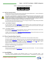
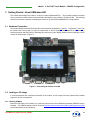
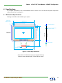
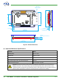
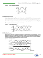
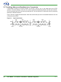
The TM4300 has been replaced by the TM4301 Features • Complete Touchscreen Module: • • • • – Projected Capacitive Multi Touch Controller – 4.3in TFT LCD – 4 Capacitive “Navigation” Keys – 200 bytes non-volatile serial EEPROM Touch: – Atmel maXTouch mXT224E Touch Controller – Supports up to 10 touches Display: – 480x272 resolution – 20 ms response time – White LED backlight Navigation Keys: – Atmel AT42QT1070 Cover Panel: – 1.2mm Soda Lime Glass – Optional 0.7mm Gorilla Glass™ PDA TM4300: 4.3in PCAP Touch Module – ARM EK Configuration 1404-5-6 Contents 1 2 Module Overview 1.1 PCB Connections 4 1.2 Host Connector J1 5 1.3 Debug Connector J2 5 1.4 Touch Sensor Flex Connector J3 6 1.5 Host Connector J4 7 1.6 Display Flex Connector J6 8 Overview of the 4.3in PCAP Touch Module – ARM EK Configuration Introduction 2.2 Understanding Unfamiliar Concepts 10 2.3 LCD Panel 10 2.4 maXTouch Capacitive Touchscreen Controller 10 2.5 2.5.1 2.6 4 5 9 maXTouch Controller Interface 11 QTouch Capacitive Button Controller 11 QTouch Controller Interface Serial EEPROM Getting Started - Atmel ARM-based EK 11 11 13 3.1 Hardware Connection 13 3.2 Loading an OS Image 13 3.2.1 Installing SAM-BA 13 3.2.2 Installing the OS Image 14 3.2.3 Using the Touch Module 14 3.2.4 Using the Touch Module 14 Specifications 15 4.1 Mechanical Specifications 15 4.2 Absolute Maximum Specifications 16 4.3 Recommended Operating Conditions 17 4.4 DC Specifications 17 4.5 I2C-compatible Bus Specifications 17 4.6 Power Consumption 17 4.7 Part Number 17 I2C Basics (I2C-compatible Operation) 5.1 2 9 2.1 2.4.1 3 4 Interface Bus PDA TM4300: 4.3in PCAP Touch Module – ARM EK Configuration 18 18 1404-5-6 TM4300: 4.3in PCAP Touch Module – ARM EK Configuration 5.2 Transferring Data Bits 18 5.3 START and STOP Conditions 18 5.4 Address Byte Format 19 5.5 Data Byte Format 19 5.6 Combining Address and Data Bytes into a Transmission 20 6 Revision History 21 7 Notes 22 The TM4300 is replaced by the TM4301 3 1 Module Overview 1.1 PCB Connections Pin 1 Touch Sensor Flex J3 D S24B 33 Pin 1 J2 Pin 1 Pin 1 Debug J4 Host Pin 1 Host AT M EL MXT224E Display J6 Flex J1 Figure 1 - PCB Connectors NOTE: Connector J6 is on the bottom side of the PCB. The following notations are used for pin descriptions: MXT QT QTouch Button Controller Serial EEPROM LCD LCD Panel I Input only OD Open drain output O Output only, push-pull P Ground or power EE 4 maXTouch touchscreen PDA TM4300: 4.3in PCAP Touch Module – ARM EK Configuration 1404-5-6 TM4300: 4.3in PCAP Touch Module – ARM EK Configuration 1.2 Host Connector J1 1 - N/C 2 P GND 3 - 4 16 I G4 17 P GND N/C 18 I B0 P GND 19 I B1 5 O ~MXT_CHG 20 I B2 6 O ~QT_CHG I B3 7 I I2C SCL 2 8 I/O 9 P I C SDA GND 10 I G7 11 P GND 12 I G5 13 P GND 14 I G6 15 P GND 21 22 I B4 23 I B5 24 I B6 25 I B7 26 I G0 27 I G1 28 I G2 29 I G3 30 P GND EE Description QT Type LCD Pin MXT EE Description QT Type LCD Pin MXT Connector J1 connects to the host and carries signals between the host and (1) the MaXTouch Touch Controller, (2) the QTouch Button Controller and (3) LCD Panel. 1.3 Debug Connector J2 1 P +5Vdc 2 O ~QT_CHG 3 O ~MXT_CHG 4 - N/C 5 I 2 I C SDA The TM4300 is replaced by the TM4301 Pin Type Description 2 QT Description MXT Type QT Pin MXT Connector J2 carries signals used to debug the MaXTouch Touch Controller and QTouch Button Controller. 6 I/O I C SCL 7 - N/C 8 P GND 9 O DBG DATA 10 O DBG CLK 5 1.4 Touch Sensor Flex Connector J3 Connector J3 connects to the touch sensor flex and carries signals used by the maXTouch controller to detect input on the touch sensor. 6 Pin Type 1 P 2 3 4 Description Pin Type Description GND 26 I/O X9 (Duplicate) P GND 27 I/O X10 I/O Y10 28 I/O X11 I/O Y9 29 I/O X12 5 I/O Y8 30 I/O X13 6 I/O Y7 31 I/O X14 7 I/O Y6 32 I/O X15 8 I/O Y5 33 I/O X16 9 I/O Y4 34 I/O X17 10 I/O Y3 35 I/O X18 11 I/O Y2 36 P GND 12 I/O Y1 37 P GND 13 I/O Y0 38 I/O Y0 14 P GND 39 I/O Y1 15 P GND 40 I/O Y2 16 I/O X0 41 I/O Y3 17 I/O X1 42 I/O Y4 18 I/O X2 43 I/O Y5 19 I/O X3 44 I/O Y6 20 I/O X4 45 I/O Y7 21 I/O X5 46 I/O Y8 22 I/O X6 47 I/O Y9 23 I/O X7 48 I/O Y10 24 I/O X8 49 P GND 25 I/O X9 50 P GND PDA TM4300: 4.3in PCAP Touch Module – ARM EK Configuration 1404-5-6 TM4300: 4.3in PCAP Touch Module – ARM EK Configuration 1.5 Host Connector J4 +5Vdc 21 P GND GND 22 P GND 3 P +5Vdc 23 - N/C 4 P GND 24 - N/C 5 I R0 25 - N/C 6 I R1 26 - N/C 7 I R2 27 - N/C 8 I R3 28 I/O 9 I R4 29 P GND 10 I R5 30 P GND 11 I R6 31 - N/C 12 I R7 32 - N/C 13 P GND 33 - N/C 14 P GND 34 - N/C 15 I DISP (Display Enable) 35 - N/C 16 I Backlight PWM 36 O Module Presence Detect 17 I VSYNC 37 - N/C 18 I HSYNC 38 - N/C 19 I DE 39 P GND 20 I PCLK 40 P GND The TM4300 is replaced by the TM4301 One-Wire Interface EE P Description QT Type LCD Pin MXT P 2 EE 1 Description QT Type LCD Pin MXT Connector J4 connects to the host and carries signals between the host and (1) the LCD Panel and (2) serial EEPROM. 7 1.6 Display Flex Connector J6 Connector J6 connects to the LCD panel flex and carries signals between the host and the LCD Panel. Note: J6 is located on the back side of the PCB. 8 Pin Type 1 P 2 3 Description Pin Type Description LED- 21 O B0 P LED+ 22 O B1 P GND 23 O B2 4 P +3.3Vdc 24 O B3 5 O R0 25 O B4 6 O R1 26 O B5 7 O R2 27 O B6 8 O R3 28 O B7 9 O R4 29 P GND 10 O R5 30 O PCLK 11 O R6 31 O DISP 12 O R7 32 O HSYNC 13 O G0 33 O VSYNC 14 O G1 34 O DE 15 O G2 35 - N/C 16 O G3 36 P GND 17 O G4 37 - N/C 18 O G5 38 - N/C 19 O G6 39 - N/C 20 O G7 40 - N/C PDA TM4300: 4.3in PCAP Touch Module – ARM EK Configuration 1404-5-6 TM4300: 4.3in PCAP Touch Module – ARM EK Configuration 2 Overview of the 4.3in PCAP Touch Module – ARM EK Configuration 2.1 Introduction The 4.3in PCAP Touch Module – ARM EK Configuration is a touchscreen module offering best-in-class projected capacitance multi-touch functionality combined with a 4.3in LCD panel. The module is configured for development and evaluation with several Atmel ARM-based EK solutions as well as development and integration with a custom host system. For convenience, this module features host interface connectors (J1 and J4) positioned for direct installation on Atmel ARM-based EK boards. As shown in Figure 2 below, the module provides host access to several sub-system components to maximize effective integration. PDA 4.3in PCAP Touch Module - ARM EK Configuration PCB Nav Keys J3 QT1070 J1 Capacitive Button Controller mXT224E Capacitive Touchscreen Controller J6 LCD Panel J4 Touch sensor HOST DS2433 Serial EEPROM Figure 2 - Functional Block Diagram The TM4300 is replaced by the TM4301 9 2.2 Understanding Unfamiliar Concepts Throughout this document, the functionality of the module sub-system will be outlined and summarized. However, the user is encouraged to refer to the resources and documents below in order to gain a more thorough understanding of each sub-system. • For a basic overview of I2C communication, refer to Section 5 of this document • Atmel maXTouch mXT224E Datasheet (www.atmel.com) • Atmel QTouch QT1070 Datasheet (www.atmel.com) • Maxim DS24B33 Datasheet (www.maximintegrated.com) In addition, when developing or evaluating with the Atmel ARM-based EK’s, it is recommended that the user visit www.at91.com which contains a broad range of resources for the EK’s and the ARM devices they feature. 2.3 LCD Panel The module provides the host with a direct connection from the host (Connector J1 and J4) to the LCD panel interface (Connector J6). Aside from generating supply voltages for the LED backlight and providing backlight control to the host, no display panel control is performed by the module. 2.4 maXTouch Capacitive Touchscreen Controller The module touch screen interface is based on the Atmel maXTouch mXT224E Touch Controller. The touch controller scans the touch sensor and will signal the host with an active low interrupt signal (Connector J1-5 ~CHG) when new touch data is available. Data communication with the maXTouch controller is performed over a shared I2C interface (Connector J1-7 SCL and J1-8 SDA). The I2C address of the touch controller can be configured by populating R5 or R8 (shown below in Figure 3) according to Table 2-1 below. The PCB ships with R5 populated – thus the I2C address is set to 0x4A by default. NOTE: Pull-up resistors for the I2C SCL and SDA lines are located at R3 and R2 respectively. A pull-up resistor for the maXTouch ~CHG interrupt signal is located at R4. AT M EL MXT 224E J3 J1 Figure 3 - Touch Controller I2C Address Selection 10 PDA TM4300: 4.3in PCAP Touch Module – ARM EK Configuration 1404-5-6 TM4300: 4.3in PCAP Touch Module – ARM EK Configuration Table 2-1 - Touch Controller I2C Address Selection R5 0Ω DNP R8 DNP 0Ω I2C Address 0x4A 0x4B Note: 0x4A is the default I2C address 2.4.1 maXTouch Controller Interface Details of the maXTouch communication protocol are beyond the scope of this document. provided below to facilitate evaluation and initial development. However information is The module is pre-loaded with a configuration already optimized for this touch sensor and panel, so the developer need only focus on interfacing with the device. When developing the maXTouch controller interface during evaluation and host development, care should be taken to avoid changing the maXTouch configuration or committing changes to NV storage on the maXTouch controller. To get started with host interface development, the user is strongly encouraged to leverage existing code available from the resources outlined in the following sections 2.4.1.1 Atmel Software Framework The Atmel Software Framework (asf.atmel.com) contains examples of code for interfacing with devices in the maXTouch family of touch controllers. The capabilities of various maXTouch devices may differ, but the basic communication protocol is common and can be applied to this module. 2.4.1.2 Linux Kernel / Android The Linux Kernel (www.kernel.org) has included basic support for maXTouch touch devices since version 2.6.36. The mainline driver has undergone considerable evolution since then. In addition, Atmel maintains patches (www.github.com/atmel-maxtouch/linux) which provide numerous out-of-cycle improvements to the mainline Linux Kernel driver. 2.5 QTouch Capacitive Button Controller The module “nav key” interface is based on the Atmel QT1070 7-Channel Capacitive Sensor Driver. The button controller scans the 4 capacitive nav keys (K1, K2, K3 and K4) and will signal the host with an active low interrupt signal (Connector J1-6 ~CHG) when a touch event has occurred. Data communication with the QT1070 controller is performed over a shared I2C interface (Connector J1-7 SCL and J1-8 SDA). The I2C address of the button controller is 0x1B and cannot be changed. NOTE: Pull-up resistors for the I2C SCL and SDA lines are located at R3 and R2 respectively. A pull-up resistor for the QTouch ~CHG interrupt signal is located at R27. 2.5.1 QTouch Controller Interface Details of the QTouch communication protocol are beyond the scope of this document. to review the QT1070 Datasheet (www.atmel.com). The user is encouraged 2.6 Serial EEPROM The module includes a DS24B33 Serial EEPROM providing 512 bytes of non-volatile storage. Data communication with the EEPROM is performed over a One-Wire Interface. The EEPROM is not used by another The TM4300 is replaced by the TM4301 11 subsystem on the touch module and can be freely used by the host system for any purpose. For example, Atmel ARM-based EK’s running Linux or Android operating systems use the pre-programmed contents of the EEPROM to identify this module type. NOTE: The user should take care when overwriting the pre-programmed EEPROM contents. As noted above, certain builds of Linux or Android targeted for the Atmel ARM-based EKs may no longer recognize the module. The user is advised to backup the EEPROM contents before overwriting. The serial EEPROM communicates via a one-wire interface (Connector J1-28). Refer to the DS24B33 Datasheet (www.maximintegrated.com) for details. 12 PDA TM4300: 4.3in PCAP Touch Module – ARM EK Configuration 1404-5-6 TM4300: 4.3in PCAP Touch Module – ARM EK Configuration 3 Getting Started - Atmel ARM-based EK This module was designed to install on a variety of Atmel ARM-based EK’s. This provides perhaps the fastest way to evaluate the performance of the touchscreen and display using a familiar, full-featured OS. The following sections will outline the process of installing the module on an Atmel AT91SAM9X35-EK running Android. 3.1 Hardware Connection The module interfaces with the EK board via the two large dual-row headers, J1 and J4. Connectors J1 and J4 on the module PCB connect with J21 and J22 respectively on the EK board (AT91SAM9X5-EK in this example). Disconnect power and USB from the EK board (and remove any other display module) before installing the touch module as shown below in Figure 4. Figure 4 – Connecting the module to the EK 3.2 Loading an OS Image In order demonstrate the complete functionality of the module, an OS image has been prepared that includes support for all of the subsystems. 3.2.1 Installing SAM-BA Before the OS image can be loaded, you must first ensure that the Atmel SAM Boot Assistant (SAM-BA) utility is installed. The SAM-BA software can be found at http://www.atmel.com/atmelsam-bain-systemprogrammer.aspx for both Windows and Linux platforms. The TM4300 is replaced by the TM4301 13 1. Remove power from the EK (J4) and remove any USB cables from the mini USB connector (J19) 2. Run the installation for the SAM-BA utility and following the installation steps until setup is complete. 3. On the Computer Module (CM) board, disable the NAND flash chip-select. (Refer to schematic for the particular CM used. For example, on the Embest 9X35 CM, SW1-1 should be switched OFF to disable NAND flash) 4. Connect power to the EK (J4) and connect a USB cable from the mini-USB connector (J19) to the computer. 5. After the USB device is recognized, a driver may be required. Point to the “drv” subfolder where SAM-BA was installed. For example, “C:\Program Files\Atmel Corporation\SAM-BA\drv” 3.2.2 Installing the OS Image Once the SAM-BA utility has been installed, the OS image can be loaded onto the EK. Download the Android OS image from http://www.pdaatl.com/modules/4.3in/sam9x35_android.zip and unzip to a working folder. Follow the procedure below to load the OS image onto the EK: 1. Remove power from the EK (J4) and remove any USB cables from the mini USB connector (J19) 2. On the Computer Module (CM) board, disable the NAND flash chip-select. (Refer to schematic for the particular CM used. For example, on the Embest 9X35 CM, SW1-1 should be switched OFF to disable NAND flash) 3. Connect power to the EK (J4) and connect a USB cable from the mini-USB connector (J19) to the computer. 4. On the CM board, enable the NAND flash chip-select. (Refer to schematic for the particular CM used. For example, on the Embest 9X35 CM, SW1-1 should be switched ON to enable NAND flash.) 5. Run the “at91SAM9x5.bat” file in the folder where the ZIP file was extracted. This will execute a script causing SAM-BA to download the various OS images to the EK. The process can take 1 or 2 minutes. 6. When the download process completes, check the “logfile.log” file. The last line of the log file should read: -I- === Successful !!! Now reboot the board === 3.2.3 Using the Touch Module Reboot the EK and wait for the OS to startup. The display should show several different progress screens – initially the Atmel logo, followed by the Android start screen, finally displaying the Android home screen. When running this Android OS image, the navigation keys function as follows: Table 3-1 - Navigation Key Function (Android) Key K1 K2 K3 K4 Navigation Function Back Menu Home Power / Sleep 3.2.4 Using the Touch Module For effective evaluation of the module – the touch sensor and the LCD panel in particular – the user is encouraged to try the following Android apps available from Google Play: TouchTest by Moonblink Dotty by Gerry Steele Multitouch Visible Test by Battery Powered Games Screen Test by Amberfog 14 PDA TM4300: 4.3in PCAP Touch Module – ARM EK Configuration 1404-5-6 TM4300: 4.3in PCAP Touch Module – ARM EK Configuration 4 Specifications For complete specifications, refer to the datasheets listed in section 2.2 for the various sub-system components outlined in sections 2.3 through 2.6. 4.1 Mechanical Specifications Drawings and CAD models available upon request. Glass Profile 124.46mm x 83.82mm R6mm in corners 108.9 mm (Sensor PET Outline) 6.53 mm (Viewable to Sensor PET Edge) 1.2 mm (Cover Panel) 95.84 mm (Viewable) LCD side User side 68.92 mm (Sensor PET Outline) 3.742 mm (Viewable to Sensor PET Edge) 54.66 mm (Viewable) Viewed from user side 0.635 mm or 0.510 (Sensor) two variants available 30.95 mm 0.076 mm (FPC) PIN 1 PIN 50 PCB contacts face down 25.5 mm (FPC Min Width) 99.2 mm (FPC Max Width) Figure 5 - Sensor Only Dimensions Sensor (P/N: 21-00002-A0) may be purchased individually. Minimum order quantities apply. Contact PDA for details. The TM4300 is replaced by the TM4301 15 Glass Profile 124.46mm x 83.82mm R6mm in corners 80.26 mm (Frame Width) 63.5 mm (PCB Width) D S24B33 10.16 mm 43.2 mm AT M EL MXT224E 17.08 mm (Cover Panel rear surface to Mounting Boss) 7.62 mm 134.62 mm (PCB Length) 5.08 mm (PCB Component Clearance) 119.5 mm (Frame Length) Figure 6 – Module Dimensions 4.2 Absolute Maximum Specifications Parameter Value Operating temp 0oC to + 70oC Storage temp -40oC to + 85oC Vdd -0.5 to +6V Max continuous pin current, any control or drive pin ±40 mA Voltage forced onto any pin -0.5V to (Vdd + 0.5) Volts CAUTION: Stresses beyond those listed under Absolute Maximum Specifications may cause permanent damage to the device. This is a stress rating only and functional operation of the device at these or other conditions beyond those indicated in the operational sections of this specification are not implied. Exposure to absolute maximum specification conditions for extended periods may affect device reliability. 16 PDA TM4300: 4.3in PCAP Touch Module – ARM EK Configuration 1404-5-6 TM4300: 4.3in PCAP Touch Module – ARM EK Configuration 4.3 Recommended Operating Conditions Parameter Value Vin 5.0V ±5 percent Supply ripple + noise ±20 mV 4.4 DC Specifications Vin = 5.0V, Vdd=3.3Vdc, Ta = recommended range, unless otherwise noted Parameter Description Min Typ Max Units Notes VIL Low input logic level - 0.5 – 0.3 Vdd V 1.8V <Vdd <3.3V VHL High input logic level 0.7 Vdd – Vdd + 0.5 V 1.8V <Vdd <3.3V VOL Low output voltage – – 0.2Vdd V VOH High output voltage 0.8Vdd – – V – – 1 µA IIL Input leakage current 4.5 I2C-compatible Bus Specifications Parameter Operation Address 0x4A or 0x4B Maximum bus speed (SCL) 400 kHz I2C Specification Version 2.1 4.6 Power Consumption Vdd (V) Mode Idd (mA) 3.3Vdc mXT224E in Free Run, LCD backlight on maximum intensity 200 4.7 Part Number Part Number 90-00002-A0 Description 4.3” Touchscreen Module For Atmel ARM EK The TM4300 is replaced by the TM4301 17 5 I2C Basics (I2C-compatible Operation) 5.1 Interface Bus The device communicates with the host over an I2C-compatible bus, in accordance with version 2.1 of the I2C specification. The following sections give an overview of the bus; more detailed information is available from www.i2C-bus.org. Devices are connected to the I2C-compatible bus as shown in Figure 7 both bus lines are connected to Vdd via pull-up resistors. The bus drivers of all I2C-compatible devices must be open-drain type. This implements a wired “AND” function that allows any and all devices to drive the bus, one at a time. A low level on the bus is generated when a device outputs a zero. Figure 7. I2C-compatible Interface Bus Vdd Device 1 Device 2 Device 3 Device n R1 R2 SDA SCL 5.2 Transferring Data Bits Each data bit transferred on the bus is accompanied by a pulse on the clock line. The level of the data line must be stable when the clock line is high; the only exception to this rule is for generating START and STOP conditions. Figure 8. Data Transfer SDA SCL Data Stable Data Stable Data Change 5.3 START and STOP Conditions The host initiates and terminates a data transmission. The transmission is initiated when the host issues a START condition on the bus, and is terminated when the host issues a STOP condition. Between the START and STOP conditions, the bus is considered busy. As shown in Figure 9 START and STOP conditions are signaled by changing the level of the SDA line when the SCL line is high. 18 PDA TM4300: 4.3in PCAP Touch Module – ARM EK Configuration 1404-5-6 TM4300: 4.3in PCAP Touch Module – ARM EK Configuration Figure 9. START and STOP Conditions SDA SCL START STOP 5.4 Address Byte Format All address bytes are 9 bits long. They consist of 7 address bits, one READ/WRITE control bit and an acknowledge bit. If the READ/WRITE bit is set, a read operation is performed. Otherwise a write operation is performed. An address byte consisting of a slave address and a READ or a WRITE bit is called SLA+R or SLA+W, respectively. When the device recognizes that it is being addressed, it acknowledges by pulling SDA low in the ninth SCL (ACK) cycle. The most significant bit of the address byte is transmitted first. Figure 10. Address Byte Format Addr MSB Addr LSB R/W ACK 7 8 9 SDA SCL 1 2 START 5.5 Data Byte Format All data bytes are 9 bits long, consisting of 8 data bits and an acknowledge bit. During a data transfer, the host generates the clock and the START and STOP conditions. The slave device is responsible for acknowledging the reception. An acknowledge (ACK) is signaled by the slave device pulling the SDA line low during the ninth SCL cycle. If the slave device leaves the SDA line high, a NACK is signaled. Figure 11. Data Byte Format Addr MSB Addr LSB R/W ACK 8 9 Aggregate SDA SDA from Transmitter SDA from Receiver SCL from Master 1 SLA+R/W The TM4300 is replaced by the TM4301 2 7 Data Byte STOP or Next Data Byte 19 5.6 Combining Address and Data Bytes into a Transmission A transmission consists of a START condition, an SLA+R or SLA+W, one or more data bytes and a STOP condition. The wired “ANDing” of the SCL line is used to implement handshaking between the host and the device. The device extends the SCL low period by pulling the SCL line low whenever it needs extra time for processing between the data transmissions. Figure 12 shows a typical data transmission. Note that several data bytes can be transmitted between the SLA+R or SLA+W and the STOP. Figure 12. Byte Transmission Addr MSB Addr LSB R/W ACK Data MSB Data LSB ACK SDA SCL 1 START 20 2 7 SLA+R/W 8 9 1 2 7 Data Byte PDA TM4300: 4.3in PCAP Touch Module – ARM EK Configuration 8 9 STOP 1404-5-6 TM4300: 4.3in PCAP Touch Module – ARM EK Configuration 6 Revision History Revision No. History Rev 1209-0-1 – Sept 2012 Initial Draft (unreleased) Rev 1209-1-2 – Sept 2012 Preliminary Draft (limited release) Rev 1210-2-3 – Oct 2012 Remove references to gesture support – not available on this module. Rev 1210-3-4 – Oct 19, 2012 Correct swapped I2C clock and data signals in Debug Connector J2 pinout table. Rev 1211-4-5 – Nov 21, 2012 Add notes to Figure 5 regarding sensor orientation and pin 1 location. Add notes to Figure 1 identifying connectors and pin 1 locations. Rev 1404-5-6 – Apr 4, 2014 Add note concerning TM4300 replaced by TM4301 TM4300 Datasheet - 20140404.docx : 4/4/2014 11:38:00 PM 4/4/2014 11:38 PM Greg Sullivan The TM4300 is replaced by the TM4301 21 7 Notes Precision Design Associates, Inc. 736 Johnson Ferry Rd, Suite C-270 Marietta, GA 30068 USA email: [email protected] tel: (770)-971-4490 ® url: http://www.pdaatl.com ® ® © 2014 Precision Design Associates. All rights reserved. Atmel , Atmel logo and combinations thereof, maXTouch , QTouch , and others are registered trademarks of Atmel Corporation or its subsidiaries. Other terms and product names may be registered trademarks or trademarks of others. 22 PDA TM4300: 4.3in PCAP Touch Module – ARM EK Configuration 1404-5-6