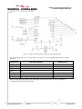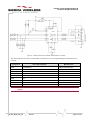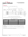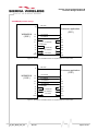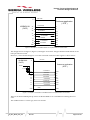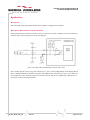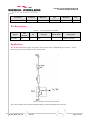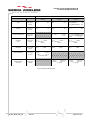
1
Product Technical Specification & Customer Design Guidelines WISMO218 WIreless Standard MOdem WA_DEV_W218_PTS_002 005 December 17, 2009 Product Technical Specification & Customer Design Guidelines Important Notice Due to the nature of wireless communications, transmission and reception of data can never be guaranteed. Data may be delayed, corrupted (i.e., have errors) or be totally lost. Although significant delays or losses of data are rare when wireless devices such as the Sierra Wireless modem are used in a normal manner with a well-constructed network, the Sierra Wireless modem should not be used in situations where failure to transmit or receive data could result in damage of any kind to the user or any other party, including but not limited to personal injury, death, or loss of property. Sierra Wireless accepts no responsibility for damages of any kind resulting from delays or errors in data transmitted or received using the Sierra Wireless modem, or for failure of the Sierra Wireless modem to transmit or receive such data. Safety and Hazards Do not operate the Sierra Wireless modem in areas where blasting is in progress, where explosive atmospheres may be present, near medical equipment, near life support equipment, or any equipment which may be susceptible to any form of radio interference. In such areas, the Sierra Wireless modem MUST BE POWERED OFF. The Sierra Wireless modem can transmit signals that could interfere with this equipment. Do not operate the Sierra Wireless modem in any aircraft, whether the aircraft is on the ground or in flight. In aircraft, the Sierra Wireless modem MUST BE POWERED OFF. When operating, the Sierra Wireless modem can transmit signals that could interfere with various onboard systems. Note: Some airlines may permit the use of cellular phones while the aircraft is on the ground and the door is open. Sierra Wireless modems may be used at this time. The driver or operator of any vehicle should not operate the Sierra Wireless modem while in control of a vehicle. Doing so will detract from the driver or operator’s control and operation of that vehicle. In some states and provinces, operating such communications devices while in control of a vehicle is an offence. WA_DEV_W218_PTS_002 Rev 005 Page 2 of 109 Product Technical Specification & Customer Design Guidelines Limitations of Liability This manual is provided “as is”. Sierra Wireless makes no warranties of any kind, either expressed or implied, including any implied warranties of merchantability, fitness for a particular purpose, or noninfringement. The recipient of the manual shall endorse all risks arising from its use. The information in this manual is subject to change without notice and does not represent a commitment on the part of Sierra Wireless. SIERRA WIRELESS AND ITS AFFILIATES SPECIFICALLY DISCLAIM LIABILITY FOR ANY AND ALL DIRECT, INDIRECT, SPECIAL, GENERAL, INCIDENTAL, CONSEQUENTIAL, PUNITIVE OR EXEMPLARY DAMAGES INCLUDING, BUT NOT LIMITED TO, LOSS OF PROFITS OR REVENUE OR ANTICIPATED PROFITS OR REVENUE ARISING OUT OF THE USE OR INABILITY TO USE ANY SIERRA WIRELESS PRODUCT, EVEN IF SIERRA WIRELESS AND/OR ITS AFFILIATES HAS BEEN ADVISED OF THE POSSIBILITY OF SUCH DAMAGES OR THEY ARE FORESEEABLE OR FOR CLAIMS BY ANY THIRD PARTY. Notwithstanding the foregoing, in no event shall Sierra Wireless and/or its affiliates aggregate liability arising under or in connection with the Sierra Wireless product, regardless of the number of events, occurrences, or claims giving rise to liability, be in excess of the price paid by the purchaser for the Sierra Wireless product. Copyright © 2009 Sierra Wireless. All rights reserved. Trademarks AirCard® and “Heart of the Wireless Machine®” are filed or registered trademarks of Sierra Wireless. Watcher® is a trademark of Sierra Wireless, registered in the European Community. Sierra Wireless, the Sierra Wireless logo, the red wave design, and the red-tipped antenna are trademarks of Sierra Wireless. , , ®, inSIM®, “YOU MAKE IT, WE MAKE IT WIRELESS®”, WAVECOM®, WISMO®, Wireless Microprocessor®, Wireless CPU®, Open AT® are filed or registered trademarks of Sierra Wireless S.A. in France and/or in other countries. Windows® is a registered trademark of Microsoft Corporation. QUALCOMM® is a registered trademark of QUALCOMM Incorporated. Used under license. Other trademarks are the property of the respective owners. WA_DEV_W218_PTS_002 Rev 005 Page 3 of 109 Product Technical Specification & Customer Design Guidelines Contact Information Sales Desk: Phone: 1-604-232-1488 Hours: 8:00 AM to 5:00 PM Pacific Time E-mail: [email protected] Post: Sierra Wireless 13811 Wireless Way Richmond, BC Canada V6V 3A4 Fax: 1-604-231-1109 Web: www.sierrawireless.com Consult our website for up-to-date product descriptions, documentation, application notes, firmware upgrades, troubleshooting tips, and press releases: www.sierrawireless.com Document Update History Rev Date List of Updates 001 April 22, 2009 Creation 002 April 28, 2009 Addition of Power Consumption table and software note in section 3.3.2 Document Cover/Footer: Updated the file name (from WA_DEV_W218_PTS_002-002 to WA_DEV_W218_PTS_002-003), the revision number and the revision date. Throughout the document: adjusted figure size to better display components and their corresponding values. § 1.1.1: Updated the 4th reference document name to Customer Process Guideline for WISMO Series. § 3.5: Changed the section title to “SPI Bus for Debug Trace ONLY”. 003 July 17, 2009 § 3.5.1: Changed the SPI-CLK Pin number from 16 to 15 Added an additional sentence at the end of the paragraph text § 3.5.1.1: Changed the value of X101 from 3.6884MHz to 3,6864MHz. § 3.11.2: Changed the PWM1 Pin number from 27 to 35. § 3.12.3: Updated the section description. § 5.2.2: Changed the Recommended connection when not used column for Pin 18, TX_CTRL from “2.8V TX Burst Indicator” to “not connected”. § 5.4: Updated the description for Class B condition. § 5.5.2: Updated the section description Deleted Figure 40: Recommended PCB landing pattern for WISMO218 WA_DEV_W218_PTS_002 Rev 005 Page 4 of 109 Product Technical Specification & Customer Design Guidelines Rev Date List of Updates § 5.5.3: Added this section. Made grammatical and other punctuation corrections throughout the document. Updated links and references. § 3.8: Changed the number of General Purpose I/Os from 11 to 3. § 3.9.2 Added a Caution box after the table. § 3.10.4.1.1 and 3.104.1.2: Removed the GND within the WISMO218 in the figures (figures 15, 16, 17 and 18) § 3.10.5.5: Added additional information in the Caution box regarding the ESD sensitivity of the audio interface. § 5.2.2: Changed the recommended connection when not in use value from “open” to “Ground” for pin #5, AUX-ADC0. § 3.10.5.5: Separated the audio track figure and the differential connection figure Labeled the differential connection figure as Figure 21 Added Figure 22: single-ended audio connection § 5.4: Updated the Class B temperature range from -30 to +75 to -40 to +85. § 5.5.3: Updated the figure to display it rotated 90 degrees counterclockwise. Updated text wording, checked for spelling and grammar, updated links and captions throughout the document. § 3.2.2: Updated the value of VBATT’s Ripple max. § 3.10.1.1: Updated table values. § 3.10.2.1.1: Updated table values. § 3.10.4.1.1: Deleted the description for Z2. § 3.13.3.1: Changed “de-assert” to “release” (re: recommendation for the ON/~OFF signal) § 3.14: Updated reference to section 3.13.3.1. § 4.1.4: Updated Caution text. § 3.10.1: Updated the DC equivalent circuit. § 3.10.1.1: Updated the table values and notes section. § 3.10.4.1.1 and 3.10.4.1.2: Updated figures from 2.85V to 2.4V § 3.13.3.1: Updated figure and included the Tready table just beneath the figure. § 3.17.3: Updated figure and updated descriptive text below the figure. § 3.13.3.1: Updated the figure to include ramp up time of VBAT. August 12, 2009 Updated the Pin Description table (Table 7) of the Main Serial Link (UART) subsection of section 3: Interfaces. Added List of Figures and List of Tables. Updated Figure 31. September 10, 2009 Added Trampup values in the Power on sequence table. Added Figure 46. Moved Recommended PCB Landing Pattern after Figure 47. WA_DEV_W218_PTS_002 Rev 005 Page 5 of 109 Product Technical Specification & Customer Design Guidelines Rev 004 Date List of Updates October 27, 2009 Updated Class A Operating Temperature Range Updated documentation reference ON/~OFF Signal: 005 November 23, 2009 Added an extra note about controlling the signal via an open collector switching transistor Updated Figure 30 to include a figure showing the signal connection via an open collector transistor Set the low level pulse length to 5.5sec Updated Figure 32 to include the 5.5s low level pulse length TX_CTRL Signal for TX Burst Indication: WA_DEV_W218_PTS_002 Rev 005 Added TX_CTRL frequency and duration Updated Figure 36 to include Tduration Updated Figure 37 (added the transistor, T601) Page 6 of 109 Product Technical Specification & Customer Design Guidelines Contents CONTENTS ....................................................................................................................... 7 LIST OF FIGURES ......................................................................................................... 12 LIST OF TABLES ........................................................................................................... 14 1. REFERENCES............................................................................................................ 16 Reference Documents ...................................................................................................................... 16 Sierra Wireless Reference Documentation................................................................................ 16 List of Abbreviations ......................................................................................................................... 16 2. GENERAL DESCRIPTION ...................................................................................... 20 General Information .......................................................................................................................... 20 Overall Dimensions ...................................................................................................................... 20 Environment and Mechanics....................................................................................................... 20 GSM/GPRS Features .................................................................................................................... 20 Interfaces....................................................................................................................................... 20 Firmware ....................................................................................................................................... 21 Connection Interfaces .................................................................................................................. 21 Functional Description ..................................................................................................................... 22 RF Functionalities......................................................................................................................... 22 Baseband Functionalities ............................................................................................................ 23 3. INTERFACES ............................................................................................................ 24 General Interfaces ............................................................................................................................. 24 Power Supply..................................................................................................................................... 25 Power Supply Description ........................................................................................................... 25 Electrical Characteristics ............................................................................................................. 26 Pin Description ............................................................................................................................. 26 Application .................................................................................................................................... 26 Recommended Components ............................................................................................................. 27 Power Consumption ......................................................................................................................... 28 Various Operating Modes ............................................................................................................ 28 Power Consumption..................................................................................................................... 29 Consumption Waveform Samples .............................................................................................. 30 Connected Mode Current Waveform................................................................................................. 31 Transfer Mode Class 10 Current Waveform ...................................................................................... 31 Idle Mode Page 2 Current Waveform ................................................................................................ 32 Idle Mode Page 9 Current Waveform ................................................................................................ 32 Recommendations for Less Consumption................................................................................. 33 Electrical Information for Digital I/O ............................................................................................. 34 WA_DEV_W218_PTS_002 Rev 005 Page 7 of 109 Product Technical Specification & Customer Design Guidelines SPI Bus for Debug Trace ONLY ..................................................................................................... 35 Pin Description ............................................................................................................................. 35 SPI Waveforms ................................................................................................................................... 35 Main Serial Link (UART) ................................................................................................................. 38 Features ......................................................................................................................................... 38 Pin Description ............................................................................................................................. 38 5-wire serial interface hardware design: ........................................................................................... 39 4-wire serial interface hardware design: ........................................................................................... 39 2-wire serial interface hardware design: ........................................................................................... 39 Application .................................................................................................................................... 40 V24/CMOS possible design ............................................................................................................... 41 SIM Interface...................................................................................................................................... 44 Features ......................................................................................................................................... 44 Pin Description ............................................................................................................................. 45 Application .................................................................................................................................... 46 SIM socket connection....................................................................................................................... 46 General Purpose Input/Output ....................................................................................................... 47 Pin Description ............................................................................................................................. 47 Analog to Digital Converter ............................................................................................................. 48 Features ......................................................................................................................................... 48 Pin Description ............................................................................................................................. 48 Analog Audio Interface .................................................................................................................... 49 Microphone Features ................................................................................................................... 49 Electrical Characteristics ................................................................................................................... 49 Speaker Features .......................................................................................................................... 50 Speakers Outputs Power ................................................................................................................... 50 Pin Description ............................................................................................................................. 51 Application .................................................................................................................................... 52 Microphone ......................................................................................................................................... 52 Recommended Components ............................................................................................................. 53 Recommended Components ............................................................................................................. 55 Speaker SPKP and SPKN .................................................................................................................. 56 Design Recommendation ............................................................................................................ 56 General ................................................................................................................................................ 56 Recommended Microphone Characteristics .................................................................................... 57 Recommended Speaker Characteristics .......................................................................................... 57 Recommended Filtering Components .............................................................................................. 57 Audio Track and PCB Layout Recommendation ............................................................................. 59 Pulse-Width Modulators (PWMs)................................................................................................... 62 Features ......................................................................................................................................... 62 Pin Description ............................................................................................................................. 62 Application .................................................................................................................................... 62 BUZZER Output ................................................................................................................................. 64 Features ......................................................................................................................................... 64 Pin Description ............................................................................................................................. 64 Application .................................................................................................................................... 65 Calculations of the Low Filter: ........................................................................................................... 66 WA_DEV_W218_PTS_002 Rev 005 Page 8 of 109 Product Technical Specification & Customer Design Guidelines Recommended characteristics for the buzzer .................................................................................. 66 ON/~OFF Signal ............................................................................................................................... 67 Features ......................................................................................................................................... 67 Pin Description ............................................................................................................................. 67 Application .................................................................................................................................... 68 Power ON ............................................................................................................................................ 68 Power OFF ........................................................................................................................................... 69 WISMO_READY Indication ............................................................................................................. 71 Features ......................................................................................................................................... 71 Pin Description ............................................................................................................................. 71 VCC_2V8 output................................................................................................................................. 72 Features ......................................................................................................................................... 72 Pin Description ............................................................................................................................. 72 Application .................................................................................................................................... 72 BAT-RTC (Backup Battery) ............................................................................................................ 73 Features ......................................................................................................................................... 73 Pin Description ............................................................................................................................. 73 Application .................................................................................................................................... 73 Super Capacitor .................................................................................................................................. 74 Non-Rechargeable Battery................................................................................................................. 74 Rechargeable Battery Cell ................................................................................................................. 75 TX_CTRL Signal for TX Burst Indication ..................................................................................... 76 Features ......................................................................................................................................... 76 Pin Description ............................................................................................................................. 77 Application .................................................................................................................................... 77 Reset .................................................................................................................................................... 78 Feature........................................................................................................................................... 78 Sequence after an external reset event (~RESET) .......................................................................... 78 Pin Description ............................................................................................................................. 78 Application .................................................................................................................................... 79 RF Interface ........................................................................................................................................ 80 RF Connection .............................................................................................................................. 80 RF Performances .......................................................................................................................... 80 Antenna Specifications................................................................................................................ 80 4. CONSUMPTION MEASUREMENT PROCEDURE ............................................ 83 Hardware Configuration .................................................................................................................. 83 Equipment ..................................................................................................................................... 83 WISMO218 Development Kit ....................................................................................................... 85 Socket-Up Board Used................................................................................................................. 86 SIM Cards Used ............................................................................................................................ 86 Software Configurations .................................................................................................................. 87 WISMO218 Configuration ............................................................................................................ 87 WA_DEV_W218_PTS_002 Rev 005 Page 9 of 109 Product Technical Specification & Customer Design Guidelines Equipment Configuration ............................................................................................................ 88 Template ............................................................................................................................................. 89 5. TECHNICAL SPECIFICATIONS........................................................................... 90 Castellation Connector Pin Configuration ................................................................................... 90 Castellation Pin ................................................................................................................................. 91 Pin-Out Description...................................................................................................................... 91 Recommended Connection When Not Used ............................................................................. 93 PCB Specification for Application Board ..................................................................................... 94 Environmental Specifications ......................................................................................................... 95 Function Status Classification .................................................................................................... 95 Class A................................................................................................................................................. 95 Class B................................................................................................................................................. 95 Mechanical Specifications............................................................................................................... 97 Physical Characteristics .............................................................................................................. 97 WISMO218 Dimensions ............................................................................................................... 98 Recommended PCB Landing Pattern ...................................................................................... 100 6. PERIPHERAL DEVICES REFERENCES ............................................................ 101 General Purpose Connector .......................................................................................................... 101 SIM Card Reader ............................................................................................................................. 101 Microphone ....................................................................................................................................... 101 Speaker ............................................................................................................................................. 101 Antenna Cable.................................................................................................................................. 101 GSM Antenna ................................................................................................................................... 102 7. NOISES AND DESIGN .......................................................................................... 103 EMC Recommendations ................................................................................................................. 103 Power Supply................................................................................................................................... 103 8. APPENDIX ............................................................................................................... 104 Standards and Recommendations ............................................................................................... 104 Safety Recommendations (for Information Only) .................................................................... 107 RF Safety ..................................................................................................................................... 107 General .............................................................................................................................................. 107 Exposure to RF Energy ..................................................................................................................... 107 Efficient Terminal Operation............................................................................................................ 107 Antenna Care and Replacement ..................................................................................................... 107 General Safety............................................................................................................................. 108 Driving ............................................................................................................................................... 108 Electronic Devices ............................................................................................................................ 108 Vehicle Electronic Equipment.......................................................................................................... 108 Medical Electronic Equipment......................................................................................................... 108 Aircraft ............................................................................................................................................... 108 Children ............................................................................................................................................. 109 WA_DEV_W218_PTS_002 Rev 005 Page 10 of 109 Product Technical Specification & Customer Design Guidelines Blasting Areas................................................................................................................................... 109 Potentially Explosive Atmospheres ................................................................................................. 109 WA_DEV_W218_PTS_002 Rev 005 Page 11 of 109 Product Technical Specification & Customer Design Guidelines List of Figures Figure 1. Functional Architecture ....................................................................................................... 22 Figure 2. Power Supply During Burst Emission ................................................................................ 25 Figure 3. Reject Filter Diagram ........................................................................................................... 26 Figure 4. SPI Timing Diagrams........................................................................................................... 35 Figure 5. Example of an SPI to UART2 Interface Conversion Implementation .............................. 36 Figure 6. Example of RS-232 Level Shifter Implementation for UART2 .......................................... 37 Figure 7. Example of RS-232 Level Shifter Implementation for UART ............................................ 40 Figure 8. Example of V24/CMOS Serial Link Implementation for 2-wire UART ............................. 41 Figure 9. Example of V24/CMOS Serial Link Implementation for 4-wire UART ............................. 41 Figure 10. Example of V24/CMOS Serial Link Implementation for 5-wire UART ............................. 42 Figure 11. Example of Full Modem V24/CMOS Serial Link Implementation for full-UART............. 42 Figure 12. Example of SIM Socket Implementation............................................................................ 46 Figure 13. DC and AC Equivalent Circuits of MIC ............................................................................... 49 Figure 14. Equivalent Circuit for SPK ................................................................................................... 51 Figure 15. Example of MIC Input Differential Connection with LC Filter .......................................... 52 Figure 16. Example of MIC Input Differential Connection without LC Filter .................................... 53 Figure 17. Example of MIC Input Single-Ended connection with LC Filter ....................................... 54 Figure 18. Example of MIC Input Single-Ended Connection without LC Filter................................. 55 Figure 19. Example of Speaker Differential Connection..................................................................... 56 Figure 20. Example of Speaker Single-Ended Connection ................................................................. 56 Figure 21. Microphone ........................................................................................................................... 57 Figure 22. Audio Track Design .............................................................................................................. 60 Figure 23. Differential Audio Connection............................................................................................. 60 Figure 24. Single-Ended Audio Connection ......................................................................................... 61 Figure 25. Relative Timing for the PWM Output ................................................................................. 62 Figure 26. Example of a LED Driven by the PWM0 or PWM1 Output ................................................ 63 Figure 27. BUZZER Output .................................................................................................................... 64 Figure 28. Example of Buzzer Implementation .................................................................................... 65 Figure 29. Example of LED Driven by the BUZZER Output ................................................................ 66 Figure 30. Transistor Example of the ON/~OFF Pin Connection Either By a Switch or Via an Open Collector 68 Figure 31. Power-ON Sequence (no PIN code activated)................................................................... 68 Figure 32. Power-OFF Sequence........................................................................................................... 70 WA_DEV_W218_PTS_002 Rev 005 Page 12 of 109 Product Technical Specification & Customer Design Guidelines Figure 33. RTC Supplied by a Gold Capacitor ..................................................................................... 74 Figure 34. RTC Supplied by a Non Rechargeable Battery.................................................................. 74 Figure 35. RTC Supplied by a Rechargeable Battery Cell .................................................................. 75 Figure 36. TX_CTRL State During TX Burst ......................................................................................... 76 Figure 37. Example of TX Status Implementation............................................................................... 77 Figure 38. Reset Timing......................................................................................................................... 78 Figure 39. Example of ~RESET Pin Connection with Push Button Configuration .......................... 79 Figure 40. Example of ~RESET Pin Connection with Transistor Configuration .............................. 79 Figure 41. Example of an RF 50 line................................................................................................... 81 Figure 42. Typical hardware configuration .......................................................................................... 84 Figure 43. WISMO218 Pin Configuration ............................................................................................. 90 Figure 44. PCB Structure Example for the Application Board ........................................................... 94 Figure 45. Environmental classes ......................................................................................................... 96 Figure 46. Castellation Pin Dimension and Location ......................................................................... 98 Figure 47. WISMO218 Dimensions ....................................................................................................... 99 WA_DEV_W218_PTS_002 Rev 005 Page 13 of 109 Product Technical Specification & Customer Design Guidelines List of Tables Table 1. Input Power Supply Voltage................................................................................................ 26 Table 2. Power Supply Pin Descriptions .......................................................................................... 26 Table 3. WISMO218 Operating Modes .............................................................................................. 28 Table 4. Consumption/Software Driver Recommendations ........................................................... 33 Table 5. Electrical Characteristics of Digital I/O .............................................................................. 34 Table 6. SPI Bus Pin Descriptions .................................................................................................... 35 Table 7. Main Serial Link Pin Descriptions ...................................................................................... 38 Table 8. Recommended Components............................................................................................... 40 Table 9. Electrical Characteristics of SIM Interface ........................................................................ 45 Table 10. SIM Interface Pin Description ............................................................................................. 45 Table 11. Recommended Components............................................................................................... 46 Table 12. Pin Description of the SIM Socket ..................................................................................... 46 Table 13. GPIO Pin Descriptions ......................................................................................................... 47 Table 14. Electrical Characteristics of ADC ....................................................................................... 48 Table 15. Analog to Digital Converter Pin Description ..................................................................... 48 Table 16. Electrical Characteristics of MIC ........................................................................................ 49 Table 17. Speaker Details .................................................................................................................... 50 Table 18. Electrical Characteristics of SPK ........................................................................................ 51 Table 19. Analog Audio Interface Pin Descriptions........................................................................... 51 Table 20. Murata Examples.................................................................................................................. 59 Table 21. PWM Electrical Characteristics .......................................................................................... 62 Table 22. PWM Pin Descriptions......................................................................................................... 62 Table 23. BUZZER Electrical Characteristics ..................................................................................... 64 Table 24. BUZZER Pin Descriptions ................................................................................................... 64 Table 25. Electrical Characteristics of the ON/~OFF Signal ............................................................ 67 Table 26. ON/~OFF Signal Pin Descriptions ..................................................................................... 67 Table 27. Electrical Characteristics of the Signal .............................................................................. 71 Table 28. WISMO_READY Indication Pin Descriptions .................................................................... 71 Table 29. Electrical Characteristics of the Signals ............................................................................ 72 Table 30. VCC_2V8 Pin Descriptions .................................................................................................. 72 Table 31. Electrical Characteristics of the Signal .............................................................................. 73 Table 32. BAT-RTC Pin Descriptions .................................................................................................. 73 Table 33. TX_CTRL Status.................................................................................................................... 76 WA_DEV_W218_PTS_002 Rev 005 Page 14 of 109 Product Technical Specification & Customer Design Guidelines Table 34. Electrical Characteristics of the Signal .............................................................................. 76 Table 35. TX_CTRL Signal Pin Descriptions ...................................................................................... 77 Table 36. Electrical Characteristics of the Signals ............................................................................ 78 Table 37. Reset Pin Descriptions ........................................................................................................ 78 Table 38. Reset Commands ................................................................................................................. 79 Table 39. Antenna Specifications........................................................................................................ 81 Table 40. Equipment Reference List ................................................................................................... 85 Table 41. Operating Mode Information ............................................................................................... 88 Table 42. WISMO218 Power Consumption ........................................................................................ 89 WA_DEV_W218_PTS_002 Rev 005 Page 15 of 109 Product Technical Specification & Customer Design Guidelines 1. References Reference Documents Several documents are referenced throughout this specification. For more details, please consult the listed reference documents. The Sierra Wireless documents referenced herein are provided in the Sierra Wireless documentation package; however, the general reference documents which are not Sierra Wireless owned are not provided in the documentation package. Sierra Wireless Reference Documentation [1] WISMO218 Hardware Presentation Reference: WA_DEV_W218_PTS_001 [2] WISMO218 AT Commands Manual Reference: WA_DEV_W218_UGD_003 [3] WISMO218 Development Kit User Guide Reference: WA_DEV_W218_UGD_004 [4] Customer Process Guideline for WISMO Series Reference: WA_DEV_WISMO_PTS_001 List of Abbreviations Abbreviation Definition AC Alternative Current ADC Analog to Digital Converter A/D Analog to Digital conversion AF Audio-Frequency AGC Automatic Gain Control AT ATtention (prefix for modem commands) AUX AUXiliary CAN Controller Area Network CB Cell Broadcast CBS Cell Broadcast Service CE - CEP Circular Error Probable CLK CLocK CMOS Complementary Metal Oxide Semiconductor WA_DEV_W218_PTS_002 Rev 005 Page 16 of 109 Product Technical Specification & Customer Design Guidelines Abbreviation Definition CODEC COder DECoder CPU Central Processing Unit CS Coding Scheme CSD Circuit Switched Data CTS Clear To Send DAC Digital to Analog Converter DAI Digital Audio Interface dB Decibel DC Direct Current DCD Data Carrier Detect DCE Data Communication Equipment DCS Digital Cellular System DR Dynamic Range DSR Data Set Ready DTE Data Terminal Equipment DTR Data Terminal Ready EFR Enhanced Full Rate E-GSM Extended GSM EMC ElectroMagnetic Compatibility EMI ElectroMagnetic Interference EMS Enhanced Message Service EN ENable ESD ElectroStatic Discharges ETSI European Telecommunications Standards Institute FIFO First In First Out FR Full Rate FTA Full Type Approval GND GrouND GPI General Purpose Input GPC General Purpose Connector GPIO General Purpose Input Output GPO General Purpose Output GPRS General Packet Radio Service GPS Global Positioning System GPSI General Purpose Serial Interface GSM Global System for Mobile communications HR Half Rate Hi Z High impedance (Z) IC Integrated Circuit IDE Integrated Development Environment WA_DEV_W218_PTS_002 Rev 005 Page 17 of 109 Product Technical Specification & Customer Design Guidelines Abbreviation Definition IF Intermediate Frequency IMEI International Mobile Equipment Identification I/O Input / Output LCD Liquid Crystal Display LED Light Emitting Diode LNA Low Noise Amplifier LSB Less Significant Bit MAX MAXimum MIC MICrophone MIN MINimum MMS Multimedia Message Service MO Mobile Originated MS Mobile Station MT Mobile Terminated na Not Applicable NF Noise Factor NMEA National Marine Electronics Association NOM NOMinal NTC Negative Temperature Coefficient PA Power Amplifier Pa Pascal (for speaker sound pressure measurements) PBCCH Packet Broadcast Control CHannel PC Personal Computer PCB Printed Circuit Board PCL Power Control Level PCM Pulse Code Modulation PDA Personal Digital Assistant PFM Power Frequency Modulation PLL Phase Lock Loop PSM Phase Shift Modulation PWM Pulse Width Modulation RAM Random Access Memory RF Radio Frequency RFI Radio Frequency Interference RHCP Right Hand Circular Polarization RI Ring Indicator RMS Root Mean Square RST ReSeT RTC Real Time Clock RTCM Radio Technical Commission for Maritime services WA_DEV_W218_PTS_002 Rev 005 Page 18 of 109 Product Technical Specification & Customer Design Guidelines Abbreviation Definition RTS Request To Send RX Receive SCL Serial CLock SDA Serial DAta SIM Subscriber Identification Module SMD Surface Mounted Device/Design SMS Short Message Service SPI Serial Peripheral Interface SPL Sound Pressure Level SPK SPeaKer SW SoftWare PSRAM Pseudo Static RAM TBC To Be Confirmed TDMA Time Division Multiple Access TP Test Point TU Typical Urban fading profile TUHigh Typical Urban, High speed fading profile TVS Transient Voltage Suppressor TX Transmit TYP TYPical UART Universal Asynchronous Receiver-Transmitter UBX µ-blox proprietary protocol (NE DOIT PAS APPARAITRE) USB Universal Serial Bus USSD Unstructured Supplementary Services Data VSWR Voltage Standing Wave Ratio WAP Wireless Application Protocol WA_DEV_W218_PTS_002 Rev 005 Page 19 of 109 Product Technical Specification & Customer Design Guidelines 2. General Description General Information The WISMO218 WIreless Standard MOdem is a self-contained EGSM/GPRS 900/1800 dual-band module that was specifically designed for M2M systems deployed in Europe and Asia. Overall Dimensions Length: 25.0 mm Width: 25.0 mm Thickness: 2.8 mm (excluding label thickness) Weight: 3.8 g Environment and Mechanics Green policy: Restriction of Hazardous Substances in Electrical and Electronic Equipment (RoHS) compliant Complete shielding The WISMO218 is compliant with RoHS Directive 2002/95/EC which sets limits for the use of certain restricted hazardous substances. This directive states that “from 1st July 2006, new electrical and electronic equipment put on the market does not contain lead, mercury, cadmium, hexavalent chromium, polybrominated biphenyls (PBB) or polybrominated diphenyl ethers (PBDE)”. GSM/GPRS Features 2 Watts EGSM 900 radio section running under 3.6 Volts 1 Watt GSM1800 radio section running under 3.6 Volts Hardware GPRS class 10 capable Interfaces VBAT power supply Digital section running under 2.8 Volts 3V/1V8 SIM interface Power supplies Serial link (UART) Analog audio ADC WA_DEV_W218_PTS_002 Rev 005 Page 20 of 109 Product Technical Specification & Customer Design Guidelines Serial bus SPI for debug trace PWM0,1 and PWM2 for buzzer output GPIOs ON/~OFF TX burst indicator Module ready indicator Reset Firmware Drives the WISMO218 via an AT command interface over a serial port Full GSM/GPRS Operating System stack Real Time Clock with calendar Connection Interfaces The WISMO218 has a 46-pin castellation form factor which provides: One ANT pin for RF in/out Other pins for baseband signals WA_DEV_W218_PTS_002 Rev 005 Page 21 of 109 Product Technical Specification & Customer Design Guidelines Functional Description The global architecture of the WISMO218 is shown below: WISMO218 Analog Interfaces Radio GSM / GPRS DSP core AUDIO ADCs Digital Interfaces UART Control & Power SPI / I2C GPIOs ARM power supplys SIM core BUZZER reset 32768 kHz PWMs RTC Memory Address Data Control Figure 1. Functional Architecture RF Functionalities The Radio Frequency (RF) range complies with the Phase II EGSM 900/DCS 1800 recommendation. The frequency range for the transmit band and receive band are listed in the table below. Transmit Band (Tx) Receive Band (Rx) E-GSM 900 880 to 915 MHz 925 to 960 MHz DCS 1800 1710 to 1785 MHz 1805 to 1880 MHz The RF part of the WISMO218 is based on a specific dual band chip which includes: a Digital low-IF receiver WA_DEV_W218_PTS_002 Rev 005 Page 22 of 109 Product Technical Specification & Customer Design Guidelines a dual-band LNAs (Low Noise Amplifier) an Offset PLL (Phase Locked Loop) transmitter a Frequency synthesizer a Digitally controlled crystal oscillator (DCXO) a Tx/Rx FEM (Front-End Module ) for dual-band GSM/GPRS Baseband Functionalities The Baseband is composed of an ARM9, a DSP and an analog element (with audio signals, I/Q signals and ADC). The core power supply is 1.2V and the digital power supply is 2.8V. WA_DEV_W218_PTS_002 Rev 005 Page 23 of 109 Product Technical Specification & Customer Design Guidelines 3. Interfaces General Interfaces The WIreless Standard MOdem, WISMO218, has a 46-pin castellation connection, which provides access to all available interfaces. The available interfaces are listed in the table below. Subsection Name Driven by AT Commands Serial Interface (SPI) No Main Serial Link Yes SIM Interface Yes General Purpose IO Yes Analog to Digital Converter No (*) Analog Audio Interface No (*) PWMs Yes PWM2 for Buzzer Output Yes ON/~OFF No Module Ready Indication No VBAT_RTC (Backup Battery) No TX Burst Indication Signal No Reset No (*) These interfaces will have AT command support in future versions. WA_DEV_W218_PTS_002 Rev 005 Page 24 of 109 Product Technical Specification & Customer Design Guidelines Power Supply Power Supply Description The power supply is one of the key elements in the design of a GSM terminal. Due to the burst emission in GSM/GPRS, the power supply must be able to deliver high current peaks in a short time. During the peaks, the ripple (Uripple) on the supply voltage must not exceed a certain limit (see Table 1 below). Listed below are the corresponding radio burst rates for the different GPRS classes in communication mode. A GSM/GPRS class 2 terminal emits 577µs radio bursts every 4.615ms. (See Figure 2 Power Supply During Burst Emission below.) VBATT Uripp Uripp t = 577 µs T = 4,615 ms Figure 2. Power Supply During Burst Emission A GPRS class 10 terminal emits 1154µs radio bursts every 4.615ms. VBATT provides for the following functions: Directly supplies the RF components with 3.6V. It is essential to keep a minimum voltage ripple at this connection in order to avoid any phase error. The peak current (1.4A peak in GSM /GPRS mode) flows with a ratio of: 1/8 of the time (around 577µs every 4.615ms for GSM /GPRS cl. 2) and 1/4 of the time (around 1154µs every 4.615ms for GSM /GPRS cl. 10) with the rising time at around 10µs. Internally used to provide, via several regulators, the supply required for the baseband signals. WA_DEV_W218_PTS_002 Rev 005 Page 25 of 109 Product Technical Specification & Customer Design Guidelines Electrical Characteristics Table 1. V MIN V NOM Input Power Supply Voltage V MAX I TYP. I MAX Ripple max (U ripp ) 10kHz to 100kHz: less than100mVpp VBATT 3.2(1) 3.6 4.8 1.35A 1.4A greater than 100kHz: less than 10mVpp (1): This value has to be guaranteed during the burst (with 1.4A Peak in GSM or GPRS mode) (2): Maximum operating Voltage Stationary Wave Ratio (VSWR) 1.5:1 When powering the WISMO218 with a battery, the total impedance (battery + protections + PCB) should be less than 150m. Pin Description Table 2. Power Supply Pin Descriptions Signal Pin Number(s) VBATT 29,30 GND 20,22,23,26,28,31 Application The reject filter can be connected between VBATT and the supply sources if the supply source is noisy. Caution: If the reject filter (C1+L1+C2) is an option, a capacitor (i.e. C2) is mandatory close to the VBATT. Filter WISMO218 L1 VBATT Supply source C1 C2 Figure 3. Reject Filter Diagram WA_DEV_W218_PTS_002 Rev 005 Page 26 of 109 Product Technical Specification & Customer Design Guidelines Recommended Components C1, C2: 10µF +/-20% Component Manufacturer GRM21BR60J106KE19L MURATA CM21X5R106M06AT KYOCERA JMK212BJ106MG-T TAYO YUDEN C2012X5R0J106MT TDK L1: 220nH +/-5% Component Manufacturer 0805CS-221XJLC COILCRAFT 0805G221J E STETCO WA_DEV_W218_PTS_002 Rev 005 Page 27 of 109 Product Technical Specification & Customer Design Guidelines Power Consumption Various Operating Modes There are various kinds of operating modes for the WISMO218 as defined in the table below. Table 3. Mode OFF Mode WISMO218 Operating Modes Description When VBATT power is supplied to the WISMO218 but has not yet been powered ON. When alarm clock is set for the WISMO218 with ALL of the following conditions: Alarm Mode before time is up with AT + CPOF having been entered from a computer that is connected to the WISMO218 with the ON/~OFF signal being left open (remains at HIGH level) Idle Mode When the WISMO218 has a location update with a live network but with no GSM/GPRS connection, while the UART interface is in sleep mode Note 1. Connected Mode The WISMO218 has GSM voice codec connection with a live network. Transfer Mode The WISMO218 has GPRS data transfer connection with a live network. Note 1 : There are two different methods to enter sleep mode through the AT command setting, AT + PSSLEEP, as described below: AT + PSSLEEP = 0 The entry of sleep mode is controlled by the level of DTR signal and the firmware. When DTR (viewed from module side) is of LOW voltage level, the WISMO218 will never enter sleep mode. When DTR (viewed from module side) is of HIGH voltage level, the WISMO218 will enter sleep mode. To wake the WISMO218 up, it is necessary to toggle the DTR (viewed from module side) from HIGH to LOW voltage level. This method should be applied if the application needs to forbid the entry of sleep mode. AT + PSSLEEP = 1 For this method, the entry of sleep mode is controlled just by the firmware. When the WISMO218 has had no activities for a certain period of time, it will enter sleep mode automatically, regardless of the DTR level. Any ASCII character on the UART can wake the WISMO218 up. For details of the AT + PSSLEEP command, please refer to document [2] WISMO218 AT Commands Manual. Note that the power consumption level will vary depending on the operating mode used. WA_DEV_W218_PTS_002 Rev 005 Page 28 of 109 Product Technical Specification & Customer Design Guidelines Power Consumption The power consumption level will vary depending on the operating mode, and it is for this reason that the following consumption values are given for each mode and RF band. The following consumption values were obtained by performing measurements on WISMO218 samples at a temperature of 25° C. Note: All of the following information given assumes a 50 RF output. Note: Power consumption performance is software related. The results listed below are based on the software version L02_00gg.WISMO218. WISMO218 Power consumption Operating mode Parameters IMIN INOM IMAX average average average VBATT=4.8V VBATT=3.6V VBATT=3.2V IMAX peak Unit -- µA Off Mode* 44 36 34 Alarm Mode 44 36 34 Paging 2 (Rx burst occurrence ~0.5s) 1.9 2.0 2.1 570 mA Paging 9 (Rx burst occurrence ~2s) 1.2 1.3 1.3 570 mA PCL5 (TX power 33dBm) 211 214 217 1400 TX mA PCL19 (TX power 5dBm) 79 82 84 220 TX mA PCL0 (TX power 30dBm) 160 163 164 950 TX mA PCL15 (TX power 0dBm) 77 80 81 200 TX mA Gam.3 (TX power 33dBm) 201 203 206 1400 TX mA Gam.17 (TX power 5dBm) 73 77 78 220 TX mA Gam.3 (TX power 30dBm) 151 154 155 950 TX mA Gam.18 (TX power 0dBm) 71 75 76 200 TX mA Gam.3 (TX power 33dBm) 366 369 373 1450 TX mA Gam.17 (TX power 5dBm) 107 111 113 240 TX mA Gam.3 (TX power 30dBm) 263 267 268 970 TX mA Gam.18 (TX power 0dBm) 103 106 108 220 TX mA Idle Mode** µA 900 MHz Connected Mode 1800MHz Transfer Mode class 8 (4Rx/1Tx) 900 MHz 1800 MHz GPRS Transfer Mode class 10 (3Rx/2Tx) * 900 MHz 1800 MHz Current consumption in OFF mode is measured with BAT-RTC being left open. ** Idle Mode consumption depends on the SIM card used. Some SIM cards respond faster than others, in which case the longer the response time is, the higher the consumption is. WA_DEV_W218_PTS_002 Rev 005 Page 29 of 109 Product Technical Specification & Customer Design Guidelines TX means that the current peak is the RF transmission burst (Tx burst). RX means that the current peak is the RF reception burst (Rx burst), in GSM mode only (worst case). Three VBATT values are used to measure the power consumption - VBATTmin (3.2V), VBATTmax (4.8V) and VBATTtyp (3.6V). The average current is given for the three VBATT values and the peak current given is the maximum current peak measured with the three VBATT voltages. For more information about the consumption measurement procedure, refer to Section 4 Consumption Measurement Procedure. Consumption Waveform Samples The consumption waveforms presented below are for an EGSM900 network configuration. The typical VBATT voltage is 3.6V. Four significant operating mode consumption waveforms are shown in the following subsections, namely: Connected Mode (PCL5: Tx power 33dBm) Transfer mode (GPRS class 10, gam.3: Tx power 33dBm ) Idle mode (Paging 2) Idle mode (Paging 9) Note that the following diagrams only show the waveform of the current, but not the exact values. WA_DEV_W218_PTS_002 Rev 005 Page 30 of 109 Product Technical Specification & Customer Design Guidelines Connected Mode Current Waveform TX PEAK Transfer Mode Class 10 Current Waveform TX PEAK WA_DEV_W218_PTS_002 Rev 005 Page 31 of 109 Product Technical Specification & Customer Design Guidelines Idle Mode Page 2 Current Waveform RX PEAK Idle Mode Page 9 Current Waveform RX PEAK WA_DEV_W218_PTS_002 Rev 005 Page 32 of 109 Product Technical Specification & Customer Design Guidelines Recommendations for Less Consumption For better power consumption, in particular for the quiescent current, it is recommended to drive the GPIOs as shown in the table below. Table 4. Signal Pin Number Consumption/Software Driver Recommendations I/O I/O Type Reset State SW Driver Recommended (Output State) GPIO1 24 I/O 2V8 Pull up 1 logic level GPIO3 16 I/O 2V8 Pull up 1 logic level GPIO5 19 I/O 2V8 Z** Input: 0 logic level Output: 1logic level GPIO2 is dedicated for WISMO_READY and is not open as GPIO purpose for customer use. GPIO4 is dedicated for TX burst indication and is not open as GPIO purpose for customer use. ** When GPIO5 is used as a general purpose output, it is necessary to have an external pull up resistor connecting to a 2.8V source. Resistance value depends on the current drain required by the application side. WA_DEV_W218_PTS_002 Rev 005 Page 33 of 109 Product Technical Specification & Customer Design Guidelines Electrical Information for Digital I/O The I/Os concerned are all interfaces such as GPIOs, SPIs, etc. Table 5. Electrical Characteristics of Digital I/O 2.8 Volts Type (2V8 ) Parameter I/O type Minim. Typ Maxim. Internal 2.8V power supply VCC_2V8 2.7V 2.8V 2.95V VIL CMOS -0.4V* - 0.4V VIH CMOS 2.4V - VCC_2V8 + 0.4V VOL CMOS - - 0.1V 2.7V - - VOH CMOS 2.4V - - Input / Output pin * Condition IOH = 4mA Absolute maximum ratings WA_DEV_W218_PTS_002 Rev 005 Page 34 of 109 Product Technical Specification & Customer Design Guidelines SPI Bus for Debug Trace ONLY The WISMO218 provides one SPI bus through the castellation pin. Pin Description Table 6. Pin Number Signal I/O SPI Bus Pin Descriptions I/O Type Reset State Description SPI-CLK 15 O 2V8 Pull down SPI Serial Clock SPI-IO 13 I/O 2V8 Pull down SPI Serial input/output SPI-O 14 O 2V8 Pull down SPI Serial input ~SPI-CS 17 O 2V8 Pull up SPI Enable SPI-IRQ 25 I 2V8 Pull down SPI Interrupt By default, the WISMO218 SPI interface is only used for monitoring trace for debug purposes. An SPI-to-UART2 conversion circuit is required to convert the SPI trace to UART2. Also, the SPI-IRQ (pin 25) is required for interrupt. Again, note that the SPI interface of the WISMO218 is not open for application use other than debug trace. SPI Waveforms Figure 4. SPI Timing Diagrams WA_DEV_W218_PTS_002 Rev 005 Page 35 of 109 Product Technical Specification & Customer Design Guidelines Figure 5. Example of an SPI to UART2 Interface Conversion Implementation The following table lists the recommended components to use in implementing the SPI to UART2 interface. Component Description/Details Manufacturer U103 SC16IS750IPW NXP Semiconductors X101 3, 6864MHz 86SMX surface mount crystal (971-3131) Farnell R104, R105 10K R106 1K C105 22pF C106 33pF C107 100nF After converting the SPI signal to a UART signal, a UART transceiver circuitry is needed to communicate this UART signal to DTE. WA_DEV_W218_PTS_002 Rev 005 Page 36 of 109 Product Technical Specification & Customer Design Guidelines Figure 6. Example of RS-232 Level Shifter Implementation for UART2 The following table lists the recommended components to use in implementing a UART transceiver circuitry. Component Description/Details Manufacturer U200 LTC2804IGN-1 LINEAR TECHNOLOGY L200 LQH2M CN100K02L MURATA J200 096615276119 SUBD9F HARTING R202 NC R204 100K C200 1µF C201 220nF C207 1µF C208 1µF Note: It is recommended to make SPI signals accessible for diagnostics by reserving some test points, for example. WA_DEV_W218_PTS_002 Rev 005 Page 37 of 109 Product Technical Specification & Customer Design Guidelines Main Serial Link (UART) A flexible 8-wire serial interface is available on the WISMO218 that complies with the V24 protocol signaling, but not with the V28 (electrical interface) due to its 2.8-Volt interface. Features The supported baud rates of the UART are 1200, 2400, 4800, 9600, 19200, 38400, 57600 and 115200 Kbits, with autobauding. The signals used by the UART are as follows: TX data (CT103/TXD) RX data (CT104/RXD) Request To Send (~CT105/RTS) Clear To Send (~CT106/CTS) Data Terminal Ready (~CT108/DTR) Data Set Ready (~CT107/DSR) Data Carrier Detect (~CT109/DCD) Ring Indicator (~CT125/RI) Pin Description Table 7. Signal Pin Number I/O Main Serial Link Pin Descriptions I/O Type Reset State Description CT103/TXD* 38 I 2V8 1 Transmit serial data CT104/RXD* 40 O 2V8 1 Receive serial data ~CT105/RTS* 39 I 2V8 0 Request To Send ~CT106/CTS* 41 O 2V8 0 Clear To Send ~CT107/DSR* 42 O 2V8 1 Data Set Ready ~CT108/DTR* 44 I 2V8 1 Data Terminal Ready ~CT109/DCD* 43 O 2V8 1 Data Carrier Detect ~CT125/RI * 45 O 2V8 1 Ring Indicator GND* * GND Ground According to PC (DTE) view The rising time and falling time of the reception signals (mainly CT103/TXD) have to be less than 300ns. Tip: The WISMO218 is designed to operate using all the serial interface signals. In particular, it is recommended to use ~CT105/RTS and ~CT106/CTS for hardware flow control in order to avoid data corruption during transmissions. WA_DEV_W218_PTS_002 Rev 005 Page 38 of 109 Product Technical Specification & Customer Design Guidelines 5-wire serial interface hardware design: Signal: CT103/TXD*, CT104/RXD*, ~CT105/RTS*, ~CT106/CTS* The signal ~CT108/DTR* must be managed following the V24 protocol signaling if we want to use idle mode. For detailed configuration, please refer to Figure 10 Example of V24/CMOS Serial Link Implementation for 5-wire UART. 4-wire serial interface hardware design: Signal: CT103/TXD*, CT104/RXD*, ~CT105/RTS*, ~CT106/CTS* The signal ~CT108/DTR* can be looped back to ~CT107/DSR from both the WISMO218 side and from the DTE side. For detailed configuration, please refer to Figure 9 Example of V24/CMOS Serial Link Implementation for 4-wire UART. 2-wire serial interface hardware design: This case is possible for a connected external chip, but it is not recommended. The flow control mechanism has to be managed from the customer side. Signal: CT103/TXD*, CT104/RXD* The signal ~CT108/DTR* can be looped back to ~CT107/DSR from both the WISMO218 side and from the DTE side. The signals ~CT105/RTS*, ~CT106/CTS* are not used, please configure using the AT command, AT + IFC = 0,0 (see document [2] WISMO218 AT Commands Manual). The signal ~CT105/RTS* can be looped back to ~CT106/CTS* from both the WISMO218 side and from the DTE side. For detailed configuration, please refer to Figure 8 Example of V24/CMOS Serial Link Implementation for 2-wire UART. Note: * The loop back connection of ~CT108/DTR* to ~CT107/DSR is not allowed when the case AT+PSSLEEP=0 is used, for which sleep mode entry is ~CT108/DTR* level dependent. (Refer to Note 1 of the Power Consumption section. In order to go to sleep mode properly under such configuration, AT+PSSLEEP=1 should be used instead. For details, please refer to document [2] WISMO218 AT Commands Manual. According to PC (DTE) view WA_DEV_W218_PTS_002 Rev 005 Page 39 of 109 Product Technical Specification & Customer Design Guidelines Application The level shifter must be a V28 electrical signal compliant with 2.8V. Figure 7. Example of RS-232 Level Shifter Implementation for UART Note that the U1 chip also protects the WISMO218 against ESD (Air Discharge) at 15KV. Table 8. Component Recommended Components Description/Details Manufacturer R1, R2 15K C1, C2, C3, C4, C5 1µF C6 100nF C7 6.8uF TANTAL 10V CP32136 AVX U1 ADM3307EACP ANALOG DEVICES J1 SUB-D9 female R1 and R2 are necessary only during Reset state to force the ~CT125/RI and ~CT109/DCD signals to HIGH level. The ADM3307EACP can be powered by the VCC_2V8 (pin 46) of the WISMO218 or by an external regulator at 2.8V. If the UART interface is connected directly to a host processor, it is not necessary to use level shifters. The interface can be connected as shown in the figure(s) below: WA_DEV_W218_PTS_002 Rev 005 Page 40 of 109 Product Technical Specification & Customer Design Guidelines V24/CMOS possible design 37 ON/~OFF Customer application ( DTE ) WISMO218 ( DCE ) 38 40 39 41 42 CT103/TXD CT104/RXD ~CT105/RTS ~CT106/CTS ~CT107/DSR Tx Rx RTS CTS DSR 44 ~CT108/DTR DTR 43 ~CT109/DCD DCD 45 ~CT125/RI GND RI GND Figure 8. Example of V24/CMOS Serial Link Implementation for 2-wire UART 37 ON/~OFF Customer application ( DTE ) WISMO218 ( DCE ) 38 40 39 41 42 CT103/TXD CT104/RXD ~CT105/RTS ~CT106/CTS ~CT107/DSR Tx Rx RTS CTS DSR 44 ~CT108/DTR DTR 43 ~CT109/DCD DCD 45 ~CT125/RI GND RI GND Figure 9. Example of V24/CMOS Serial Link Implementation for 4-wire UART WA_DEV_W218_PTS_002 Rev 005 Page 41 of 109 Product Technical Specification & Customer Design Guidelines 37 ON/~OFF Customer application ( DTE ) WISMO218 ( DCE ) 38 40 39 41 CT103/TXD CT104/RXD ~CT105/RTS ~CT106/CTS ~CT107/DSR 42 44 ~CT108/DTR 43 ~CT109/DCD 45 ~CT125/RI GND Tx Rx RTS CTS DSR DTR DCD RI GND Figure 10. Example of V24/CMOS Serial Link Implementation for 5-wire UART The designs shown in Figure 8, Figure 9, and Figure 10 are basic designs. Both the DCD and RI can be left open when not used. However, a more flexible design to access this serial link with all modem signals is shown below. WISMO218 ( DCE ) 37 ON/~OFF Customer application ( DTE ) 2.8Volt 2x 10K 43 ~CT109/DCD 45 ~CT125/RI CT103/TXD 38 CT104/RXD 40 ~CT105/RTS 39 ~CT106/CTS 41 ~CT107/DSR 42 ~CT108/DTR 44 GND GND DCD RI Tx Rx RTS CTS DSR DTR GND Figure 11. Example of Full Modem V24/CMOS Serial Link Implementation for full-UART There is an internal 10K pull-up resistor on RI and DCD to set it to HIGH level during the reset state. The UART interface is a 2.8V type, but is 3V tolerant. WA_DEV_W218_PTS_002 Rev 005 Page 42 of 109 Product Technical Specification & Customer Design Guidelines Tip: The WISMO218 UART is designed to operate using all the serial interface signals. In particular, it is recommended to use ~CT105/RTS and ~CT106/CTS for hardware flow control in order to avoid data corruption during transmission. WA_DEV_W218_PTS_002 Rev 005 Page 43 of 109 Product Technical Specification & Customer Design Guidelines SIM Interface The Subscriber Identification Module can be directly connected to the WISMO218 through this dedicated interface. Features The SIM interface controls both 1.8V and 3V SIM cards. It is recommended to add Transient Voltage Suppressor diodes (TVS) on the signal connected to the SIM socket in order to prevent any Electrostatic Discharge. TVS diodes with low capacitance (less than 10pF) have to be connected on SIM-CLK and SIM-IO signals to avoid any disturbance from the rising and falling edge. These types of diodes are mandatory for the Full Type Approval. They will be placed as close as possible to the SIM socket. The recommended low capacitance diode array to use is the DALC208SC6 from ST Microelectronics. The SIM uses four (4) signals, namely: SIM-VCC: SIM power supply ~SIM-RST: reset SIM-CLK: clock SIM-IO: I/O port The SIM interface controls a 3V/1V8 SIM. This interface is fully compliant with the GSM 11.11 recommendations concerning SIM functions. WA_DEV_W218_PTS_002 Rev 005 Page 44 of 109 Product Technical Specification & Customer Design Guidelines Table 9. Parameter Electrical Characteristics of SIM Interface Conditions Minim. Typ Maxim. Unit SIM-IO VIH IIH = ± 20µA 0.7xVSIM - - V SIM-IO VIL IIL = 1mA - - 0.4 V ~SIM-RST, SIM-CLK VOH Source current = 20µA 0.9xVSIM - - V SIM-IO VOH Source current = 20µA 0.8xVSIM - - V ~SIM-RST, SIM-IO, SIMCLK VOL Sink current = -200µA - - 0.4 V SIM-VCC = 2.9V 2.75 2.9 3.0 V SIM-VCC = 1.8V 1.65 1.8 1.95 V full-power mode - - 20 mA Sleep mode with 32kHz system clock enabled. - - 3 mA SIM-CLK Rise/Fall Time Loaded with 30pF and ESD protection diode - 25 50 ns ~SIM-RST, Rise/Fall Time Loaded with 30pF and ESD protection diode - 45 - ns SIM-VCC Output Voltage SIM-VCC current SIM-IO Rise/Fall Time Loaded with 30pF and ESD protection diode - 0.2 1 µs SIM-CLK Frequency Loaded with 30pF - - 3.25 MHz Pin Description Table 10. Signal Pin Number I/O SIM Interface Pin Description Reset State I/O Type Description Multiplexed with SIM-CLK 9 O 2V9 / 1V8 0 SIM Clock Not mux ~SIM-RST 11 O 2V9 / 1V8 0 SIM Reset Not mux SIM-IO 10 I/O 2V9 / 1V8 Pull up SIM Data Not mux SIM-VCC 8 O 2V9 / 1V8 SIM Power Supply Not mux WA_DEV_W218_PTS_002 Rev 005 Page 45 of 109 Product Technical Specification & Customer Design Guidelines Application Figure 12. Example of SIM Socket Implementation Table 11. Component Recommended Components Description/Details Manufacturer C400 100nF D400 ESDA6V1SC6 ST D401 DALC208SC6 SGS-THOMSON J400 ITT CANNON CCM03 series (See the SIM Card Reader sub-section for more information) CANNON SIM socket connection Table 12. Signal Pin Description of the SIM Socket Pin Number Description VCC 1 SIM-VCC RST 2 ~SIM-RST CLK 3 SIM-CLK CC4 4 Not connected GND 5 GROUND VPP 6 Not connected I/O 7 SIM-IO CC8 8 Not connected Note: CC4 and CC8 are not connected as the WISMO218 does not support SIM detect feature. WA_DEV_W218_PTS_002 Rev 005 Page 46 of 109 Product Technical Specification & Customer Design Guidelines General Purpose Input/Output The WISMO218 provides up to 3 General Purpose I/Os. They are used to control any external device such as an LCD or a Keyboard backlight. These GPIOs offer the possibility to read the pin state whatever their direction may be. Pin Description Table 13. Signal Pin Number GPIO Pin Descriptions I/O I/O Type Reset State GPIO1 24 I/O 2V8 Pull up GPIO3 16 I/O 2V8 Pull up GPIO5 19 I/O 2V8 Pull down GPIO2 is dedicated for WISMO_READY and is not open as GPIO purpose for customer use. GPIO4 is dedicated for TX burst indication and is not open as GPIO purpose for customer use. When GPIO5 is used as a general purpose output, it is necessary to have an external pull up resistor connecting to a 2.8V source. Resistance value depends on the current drain required by the application side. WA_DEV_W218_PTS_002 Rev 005 Page 47 of 109 Product Technical Specification & Customer Design Guidelines Analog to Digital Converter One Analog to Digital Converter input is provided by the WISMO218. It is a 10-bit resolution converter, ranging from either 0 to 1V or 0 to 3V, depending on the general purpose input mode. Features The AUX-ADC0 input can be used for customer applications. Table 14. Electrical Characteristics of ADC Parameter Min Typ Max Unit Resolution - 10 - bits Sampling frequency - - 200 kHz 1 general purpose input 0 - 1 V 1 general purpose input in div-by-3 mode 0 - 3 V Integral non-linearity (INL) -2.5 - +2.5 bit Differential non-linearity (DNL) -1 - +3 bit input resistance 120 - - K input capacitance - - 10 pF Input signal range Input impedance Pin Description Table 15. Signal AUX-ADC0 Analog to Digital Converter Pin Description Pin Number 5 I/O I I/O Type Analog Description A/D converter Caution: The AUX-ADC0 pin is ESD sensitive. It is a must to add ESD protection to this pin once it is externally accessible. Recommended ESD protection: AVL5M02200 from Amotech. WA_DEV_W218_PTS_002 Rev 005 Page 48 of 109 Product Technical Specification & Customer Design Guidelines Analog Audio Interface The WISMO218 supports one microphone input and one speaker output. It also includes an echo cancellation feature which allows hands free function. In some cases, ESD protection must be added on the audio interface lines. Microphone Features The microphone, MIC, can either have a single-ended or a differential connection. However, it is strongly recommended to use a differential connection in order to reject common mode noise and TDMA noise. When using a single-ended connection, be sure to have a very good ground plane, very good filtering as well as shielding in order to avoid any disturbance on the audio path. The gain of MIC inputs is internally adjusted and can be tuned using AT commands. The MIC already includes suitable biasing for an electret microphone. The electret microphone can then be connected directly on the inputs for easy connection. AC coupling is also already embedded in the WISMO218. DC Equivalent Circuit MICP R2 MICN R2 AC Equivalent Circuit Z2 MICP MIC2+ MICN Z2 GND Do cu me Min nt Typ 2.4 Titl 2.4 e 1.2 GND Figure 13. DC and AC Equivalent Circuits of MIC Electrical Characteristics Table 16. Electrical Characteristics of MIC Parameters Internal biasing DC Characteristics MICP - MICN without 2.2K to GND - MICN with 2.2K to GND - Output current R2 AC Characteristics WA_DEV_W218_PTS_002 Z2 MICP (MICN=Open) Rev 005 - Do2.2 cu2.2 me nt Titl Max Unit - V - V - V mA - K K Page 49 of 109 Product Technical Specification & Customer Design Guidelines Parameters 200 Hz<F<4 kHz Min Max Unit Z2 MICN (MICP=Open) Z2 MICP (MICN=GND) 2.2 Z2 MICN (MICP=GND) Maximum working voltage ( MICP-MICN) (THD 10%) Typ Impedance between MICP and MICN without 2.2K to GND 4.5 Impedance between MICP and MICN with 2.2K to GND 3.2 AT+VGT*=1 Maximum rating voltage (MICP or MICN) - - 210 -0.5 - 4.4 mVpp V * The input voltage depends on the input micro gain set by the AT command. Please refer to the document [2], WISMO218 AT Commands Manual. ** Because both MICP and MICN are internally biased, it is necessary to use a coupling capacitor to connect an audio signal provided by an active generator. Only a passive microphone can be directly connected to the MICP input. Speaker Features The speaker, SPK, can either have a single-ended or a differential connection. However, it is strongly recommended to use a differential connection in order to reject common mode noise and TDMA noise. Moreover, in single-ended mode, half (½) of the power is lost. When using a single-ended connection, be sure to have a very good ground plane, very good filtering as well as shielding in order to avoid any disturbance on the audio path. Table 17. Parameter Speaker Details Typ Unit Connection Z (SPKP, SPKN) 16 or 32 Differential mode Z (SPKP, SPKN) 8 Single-ended mode Speakers Outputs Power The maximal specifications given below are available with the maximum power output configuration values set by an AT command. The typical values are recommended. WA_DEV_W218_PTS_002 Rev 005 Page 50 of 109 Product Technical Specification & Customer Design Guidelines SPK Outputs The SPK interface allows for both differential and single ended speaker connections. WISMO218 SPKN SPKP Figure 14. Equivalent Circuit for SPK Table 18. _ Electrical Characteristics of SPK Parameters Biasing voltage Min Typ Max Unit SPKP and SPKN - 1.4 - V RL=8: AT+VGR=6*; single ended - - 1 Vpp RL=8: AT+VGR=6*; differential - - 2 Vpp RL=16 or 32: AT+VGR=6*; single ended - - 1.1 Vpp RL=16 or 32: AT+VGR=6*; differential - - 2.2 Vpp RL Load resistance 6 8 - IOUT Output current; peak value; RL=8 - - 90 mA POUT RL=8; AT+VGR=10*; - - 65 mW Output swing voltage * The output voltage depends on the output speaker gain set by the AT command. Please refer to document [2] WISMO218 AT Commands Manual. If a single-ended connection is used, only SPKP has to be connected. The result is a maximal output power divided by 2. Pin Description Table 19. Signal Pin Number I/O Analog Audio Interface Pin Descriptions I/O Type Description MICP 3 I Analog Microphone positive input MICN 4 I Analog Microphone negative input SPKP 1 O Analog Speaker positive output SPKN 2 O Analog Speaker negative output WA_DEV_W218_PTS_002 Rev 005 Page 51 of 109 Product Technical Specification & Customer Design Guidelines Application Microphone The following subsections define different microphone configuration examples. Microphone Differential Connection Example When a differential connection of MIC is used, it is necessary to add a 2.2K resistor from MICN to GND in order to have proper bias of the microphone. Figure 15. Example of MIC Input Differential Connection with LC Filter Note: Audio quality can be very good without L1, L2, C2, C3 and C4 depending on the design. But if there is EMI perturbation, this filter can reduce the TDMA noise. This filter (L1, L2, C2, C3 and C4) is not mandatory. If not used, the capacitor must be removed and the coil replaced by a 0 resistor as the shown in the following schematic. WA_DEV_W218_PTS_002 Rev 005 Page 52 of 109 Product Technical Specification & Customer Design Guidelines Figure 16. Example of MIC Input Differential Connection without LC Filter The capacitor C1 is highly recommended to eliminate TDMA noise. Note that C1 must be close to the microphone. Recommended Components Component Description/Details Notes C1 12pF to 33pF needs to be tuned depending on the design C2, C3, C4 47pF needs to be tuned depending on the design L1, L2 100nH needs to be tuned depending on the design Microphone Single-Ended Connection Example When single-ended connection is used for MIC, MICN is just left open. WA_DEV_W218_PTS_002 Rev 005 Page 53 of 109 Product Technical Specification & Customer Design Guidelines Figure 17. Example of MIC Input Single-Ended connection with LC Filter *Z2 is from 200Hz to 4kHz. For more characteristics refer to the Electrical Characteristics section. Note that: Internal input impedance value becomes 1100, due to the connection of the other end to ground. The single ended design is very sensitive to TDMA noise. It is recommended to add L1 and C2 footprint as an LC filter to try to eliminate TDMA noise. A very good grounding on the MIC is a must in order to ensure good audio performance against TDMA. Also, special care on the PCB layout must be taken. When not used, the filter can be removed by replacing L1 with a 0 resistor and by disconnecting C2, as shown in the following schematic. WA_DEV_W218_PTS_002 Rev 005 Page 54 of 109 Product Technical Specification & Customer Design Guidelines Figure 18. Example of MIC Input Single-Ended Connection without LC Filter *Z2 is from 200Hz to 4kHz. For more characteristics refer to the Electrical Characteristics section. The capacitor C1 is highly recommended to eliminate TDMA noise. Note that C1 must be close to the microphone. Recommended Components Component C1 Description/Details 12pF to 33pF Notes needs to be tuned depending on the design C2 needs to be tuned depending on the design L1 needs to be tuned depending on the design WA_DEV_W218_PTS_002 Rev 005 Page 55 of 109 Product Technical Specification & Customer Design Guidelines Speaker SPKP and SPKN SPK Differential Connection SPKP SPKN Figure 19. Example of Speaker Differential Connection SPK Single-Ended Connection Typical implementation: C1 + Speaker Z hp 33 pF to 100 pF SPKP C3 X SPKN Figure 20. Example of Speaker Single-Ended Connection 4.7µF < C1 < 47 µF (Depending on speaker characteristics and output power.) Using a single-ended connection includes losing output power (-6dB) as compared to a differential connection. The connection between the WISMO218 pins and the speaker must be designed to keep the serial impedance lower than 1.5 in a single-ended connection. SPKN can be left open in a single-ended connection. Design Recommendation General When both speaker and microphone are exposed to the external environment, it is recommended to add ESD protection as close as possible to the speaker or microphone, connected between the audio lines and a good ground. When using the single-ended connection of MICP, ensure to have a good ground plane, good filtering as well as shielding, in order to avoid any disturbance on the audio path. WA_DEV_W218_PTS_002 Rev 005 Page 56 of 109 Product Technical Specification & Customer Design Guidelines It is important to select an appropriate microphone, speaker and filtering components to avoid TDMA noise. Recommended Microphone Characteristics The impedance of the microphone has to be around 2K. Sensitivity is from -40dB to –50 dB. SNR > 50 dB. Frequency response is compatible with the GSM specifications. To suppress TDMA noise, it is highly recommended to use microphones with two internal decoupling capacitors: CM1=56pF (0402 package) for the TDMA noise coming from the demodulation of the GSM900 frequency signal CM2=15pF (0402 package) for the TDMA noise coming from the demodulation of the DCS frequency signal The capacitors have to be soldered in parallel to the microphone: CM Figure 21. Microphone Recommended Speaker Characteristics Type of speakers: Electro-magnetic /10mW Impedance: 8 for hands-free Impedance: 32 for heads kit Sensitivity: 110dB SPL min Receiver frequency response is compatible with the GSM specifications. Recommended Filtering Components When designing a GSM application, it is important to select the right audio filtering components. The strongest noise, called TDMA, is mainly due to the demodulation of the GSM900 and DCS1800 signal: A burst is produced every 4.615ms; where the frequency of the TDMA signal is equal to 216.7Hz plus harmonics. The TDMA noise can be suppressed by filtering the RF signal using the right decoupling components. WA_DEV_W218_PTS_002 Rev 005 Page 57 of 109 Product Technical Specification & Customer Design Guidelines The types of filtering components are: RF decoupling inductors RF decoupling capacitors A good “Chip S-Parameter” simulator is proposed by Murata. Refer to http://www.murata.com/products/design_support/mcsil/index.html for more details. Using different Murata components, we could see that the value, the package and the current rating can have different decoupling effects. WA_DEV_W218_PTS_002 Rev 005 Page 58 of 109 Product Technical Specification & Customer Design Guidelines The table below shows some examples with different Murata components: Table 20. Murata Examples Package Filtered band 0402 GSM900 GSM 850/900 DCS/PCS Value 100nH 56pF 15pF Types Inductor Capacitor Capacitor Position Serial Shunt Shunt Manufacturer Murata Murata Murata Rated 150mA 50V 50V LQG15HSR10J02 or LQG15HNR10J02 GRM1555C1H560JZ01 GRM1555C1H150JZ01 or GRM1555C1H150JB01 Reference Package Filtered band 0603 GSM900 GSM 850/900 DCS/PCS Value 100nH 47pF 10pF Types Inductor Capacitor Capacitor Position Serial Shunt Shunt Manufacturer Murata Murata Murata Rated 300mA 50V 50V LQG18HNR10J00 GRM1885C1H470JA01 or GRM1885C1H470JB01 GRM1885C1H150JA01 or GQM1885C1H150JB01 Reference Audio Track and PCB Layout Recommendation To avoid TDMA noise, it is recommended to surround the audio tracks with ground as shown in the following figure: WA_DEV_W218_PTS_002 Rev 005 Page 59 of 109 Product Technical Specification & Customer Design Guidelines Figure 22. Audio Track Design For differential connections, it is necessary to add a 2.2KΩ resistor from MICN to GND to have a proper bias of the microphone. Refer to the following figure. Differential Audio line is always in parallel Figure 23. Differential Audio Connection For single-ended connections, the negative pole of the microphone, MICN, should be connected to GND. Refer to the following figure. WA_DEV_W218_PTS_002 Rev 005 Page 60 of 109 Product Technical Specification & Customer Design Guidelines Figure 24. Single-Ended Audio Connection Caution: It is a must to avoid digital tracks crossing under and over the audio tracks. Even when MICP is singled-ended, it is highly recommended to have the MIC ground and the LC filter ground to act as an audio analog ground during the PCB layout. This audio ground, together with the MICP signal, should act as the differential line pair. And this audio ground should only be connected to the WISMO218 module ground as close as possible to the castellation GND pin of WISMO218. It is the same case for SPKP and SPKN. Also, the audio interface is ESD sensitive. It is a must to add ESD protection to the interface once it is externally accessible. Recommended ESD protection: ESDA6VIL from ST. WA_DEV_W218_PTS_002 Rev 005 Page 61 of 109 Product Technical Specification & Customer Design Guidelines Pulse-Width Modulators (PWMs) The WISMO218 contains two Pulse-Width Modulators (PWMs). They can be used in conjunction with an external transistor for driving a vibrator, or a backlight LED. Features Each PWM uses two 7-bit unsigned binary numbers: one for the output period and one for the pulse width or the duty cycle. The relative timing for the PWM output is shown in the figure below. Figure 25. Relative Timing for the PWM Output Table 21. Parameter PWM Electrical Characteristics Condition Minimum Typical Maximum Unit High impedance load 2.7 2.85 - V Load with IoH = 4mA - 2.4 - V V OL - - - 0.1 V I PEAK - - - 4 mA Frequency - 25.6 - 1083.3 kHz Duty cycle - 0* - 100* % V OH Pin Description Table 22. Signal Pin Number PWM Pin Descriptions I/O I/O Type Description PWM0 36 O 2V8 PWM output PWM1 35 O 2V8 PWM output Application Both the PWM0 and PWM1 signals can be used in conjunction with an external transistor for driving a vibrator, or a backlight LED. WA_DEV_W218_PTS_002 Rev 005 Page 62 of 109 Product Technical Specification & Customer Design Guidelines Figure 26. Example of a LED Driven by the PWM0 or PWM1 Output The value of R607 can be harmonized depending on the LED (D605) characteristics. The recommended digital transistor to use for T601 is the DTC144EE from ROHM. WA_DEV_W218_PTS_002 Rev 005 Page 63 of 109 Product Technical Specification & Customer Design Guidelines BUZZER Output The signal BUZZER outputs a square wave at the desired tone frequency. The tone frequencies are programmable and can be re-programmed on-the-fly to generate monophonic audio ringtones or alert tones. The tone level can also be adjusted in 4dB steps, or it can be muted. Features The signal BUZZER can be used in conjunction with an external transistor/MOSFET for driving a buzzer in order to give a maximum current of 100mA (PEAK) and an average of 40mA, depending on application requirement. Figure 27. BUZZER Output Table 23. Parameter BUZZER Electrical Characteristics Condition Minimum Typical Maximum Unit High impedance load 2.7 2.85 - V Load with IoH = 4mA - 2.4 - V IPEAK - - - 4 mA VOL - - - 0.1 V Frequency - 200 - 2500 Hz Duty cycle - 0* - 100* % Tone level 4 dB step -24 - 0 dB VOH * Be mindful of the maximum frequency and the minimum/maximum duty cycle. There is a limitation due to the RC environment. The amplitude modulation becomes less fine when the set limits are reached. Pin Description Table 24. Signal BUZZER Pin Number 34 WA_DEV_W218_PTS_002 I/O O Rev 005 BUZZER Pin Descriptions I/O Type 2.8V Description Buzzer output Page 64 of 109 Product Technical Specification & Customer Design Guidelines Application The maximum peak current of the transistor/MOSFET is 100mA and the maximum average current is 40mA, while the peak current of the BUZZER pin should be less than 4mA. A diode against transient peak voltage must be added as shown below. VBATT R1 C1 D1 T1 WISMO218 R2 BUZZER 34 R3 GND GND Figure 28. Example of Buzzer Implementation Where: R1 must be chosen in order to limit the current at IPEAK max of 100mA and must be adjusted in function of the frequency and the duty cycle used. D1 = BAV70T-7 or BAS16 (for example) T1 = FDN335N (for example) R2 = 0 R3 = 1M A low filter is recommended at low frequencies. WA_DEV_W218_PTS_002 Rev 005 Page 65 of 109 Product Technical Specification & Customer Design Guidelines Calculations of the Low Filter: Req is the total resistor in line. C is the capacitive charge on T1 and the ground. The cut-off frequency (Fc) must be higher than FBUZZ-OUT. Due to the conception of this signal, the frequency modulation of the BUZZER signal is 64* FBUZZOUT. Fc must be at least 64 * FBUZZ-OUT. Fc = 1/ (2. .Req.C) Recommended characteristics for the buzzer Electro-magnetic type Impedance: 7 to 30 Sensitivity: 90 dB SPL min @ 10 cm Current: 60 to 90mA The BUZZER output can also be used to drive a LED as shown in the figure below: Figure 29. Example of LED Driven by the BUZZER Output The value of R607 can be harmonized depending on the LED (D605) characteristics. The recommended digital transistor to use for T601 is the DTC144EE from ROHM. WA_DEV_W218_PTS_002 Rev 005 Page 66 of 109 Product Technical Specification & Customer Design Guidelines ON/~OFF Signal The ON/~OFF pin is used to switch ON or switch OFF the WISMO218. ON/~OFF signal is internally connected to the permanent 3.0V supply regulator inside the WISMO218 via a pull-up resistor. Once there is VBATT supply to the WISMO218, this 3.0V supply regulator will be enabled and so the ON/~OFF signal is by default at HIGH level. A LOW level signal has to be provided on the ON/~OFF pin to switch ON the WISMO218. Caution: All external signals must be inactive when the WISMO218 is OFF to avoid any damage when starting and to allow the WISMO218 to start and stop correctly. Avoid using application MCU GPIO to directly control the ON/~OFF signal of the WISMO218; instead, control this signal via an open collector switching transistor. Features Table 25. Parameter I/O Type Electrical Characteristics of the ON/~OFF Signal Minimum Typ. Maximum Unit VIH 2V8 2.4 - 3.0 V VIL 2V8 - - 0.4 V Pin Description Table 26. Signal ON/~OFF Pin Number 37 WA_DEV_W218_PTS_002 I/O I Rev 005 ON/~OFF Signal Pin Descriptions I/O Type 2V8 Description WISMO218 Power ON/OFF Page 67 of 109 Product Technical Specification & Customer Design Guidelines Application Switch 1 2 ON/~OFF 3 GND Figure 30. Example of the ON/~OFF Pin Connection Either By a Switch or Via an Open Collector Transistor Power ON Figure 31. Power-ON Sequence (no PIN code activated) WA_DEV_W218_PTS_002 Rev 005 Page 68 of 109 Product Technical Specification & Customer Design Guidelines Min Typ. Max Unit Tready 4 5 7 s Trampup - - 120 ms The ON/~OFF signal level is detected about 250ms after VBATT is available. Note that this timing might be temperature dependant. The voltage of this signal has to be pulled LOW for at least 685ms for powering ON. Within this 685ms, the WISMO_READY signal will initially reset to HIGH for about 135ms and then resume to LOW. During the power ON sequence, an internal reset is automatically performed for 38ms (typically). During this phase, any external reset should be avoided. Once the WISMO218 is properly powered ON, the WISMO_READY pin will set to HIGH level to acknowledge the successful powering ON of the WISMO218 before it is ready to operate. The ON/~OFF signal can be left at LOW level until power off. Please note that temperature conditions may affect the timing for powering up. The recommended way to release the ON/~OFF signal is to detect the WISMO_READY signal within 685ms of powering ON while the level pulse of the ON/~OFF signal is set to LOW, and wait until the WISMO_READY signal goes HIGH again. Power OFF The WISMO218 can be powered off by either software or hardware. Software power off AT command: AT+CPOF is used to power off the WISMO218. Note: If the ON/~OFF pin is maintained at LOW level when AT+CPOF is used, the module can’t be switched OFF. Hardware power off A LOW level pulse is applied on the ON/~OFF pin for 5.5sec. AT+CPOF will then be automatically sent to the WISMO218. Once the WISMO218 receives the AT+CPOF command, the WISMO218 will be deregistered from the network. The WISMO_READY pin will become LOW to indicate that AT commands are no longer available for the WISMO218. If the ON/~OFF signal is HIGH, then the WISMO218 will also be switched off. WA_DEV_W218_PTS_002 Rev 005 Page 69 of 109 Product Technical Specification & Customer Design Guidelines Figure 32. Power-OFF Sequence WA_DEV_W218_PTS_002 Rev 005 Page 70 of 109 Product Technical Specification & Customer Design Guidelines WISMO_READY Indication This signal indicates the ready status of the WISMO218 after powering on. Please note that there is an initial positive pulse of less than 200ms during power ON. For details, please refer to the power ON diagram in the Power ON sub-section. Once the WISMO218 is properly powered ON, the WISMO_READY pin will set to HIGH level to acknowledge the successful powering ON of the WISMO218 before it is ready to operate. On the other hand, the level will go LOW before powering off. Features Table 27. Parameter I/O Type Electrical Characteristics of the Signal Minimum Typ. Maximum Unit VOH 2V8 2.7 2.8 2.95 V VOL 2V8 - - 0.4 V Pin Description Table 28. Signal WISMO_READY WA_DEV_W218_PTS_002 Pin Number 7 WISMO_READY Indication Pin Descriptions I/O O Rev 005 I/O Type 2V8 Description WISMO218 ready indication Page 71 of 109 Product Technical Specification & Customer Design Guidelines VCC_2V8 output The VCC_2V8 output can only be used for pull-up resistor(s) and as a reference supply. This voltage supply is available when the WISMO218 is switched on. Features Table 29. Electrical Characteristics of the Signals Parameter Minimum Output voltage VCC_2V8 Output Current Typ Maximum Unit 2.70 2.80 2.95 V Full-power mode - - 50 mA Sleep mode - - 3 mA Pin Description Table 30. Signal VCC_2V8 Pin Number 46 VCC_2V8 Pin Descriptions I/O O I/O Type Supply Description Digital supply Application This digital power supplies are mainly used to: Pull-up signals such as I/O Supply the digital transistors driving LEDs Act as a voltage reference for ADC interface AUX-ADC0 WA_DEV_W218_PTS_002 Rev 005 Page 72 of 109 Product Technical Specification & Customer Design Guidelines BAT-RTC (Backup Battery) The WISMO218 provides an input/output to connect a Real Time Clock power supply. Features This pin is used as a back-up power supply for the internal Real Time Clock. The RTC is supported by the WISMO218 when VBATT is available but a back-up power supply is needed to save date and hour when VBATT is switched off. If the RTC is not used, this pin can be left open. If VBATT is available, the back-up battery can be charged by the internal 3.0V power supply regulator via a 2K resistor implemented inside the WISMO218. Table 31. Electrical Characteristics of the Signal Parameter Minimum Typ Maximum Unit Input voltage - 3.0 - V Input current consumption* - 2.5 - µA Output voltage 2.82 3.0 3.18 V Max charging current (@VBATT=3.6V) - 0.6 - mA * Provided by an RTC back-up battery when the WISMO218 is off and VBATT = 0V. Pin Description Table 32. Signal BAT-RTC Pin Number 6 I/O I/O BAT-RTC Pin Descriptions I/O Type Supply Description RTC Back-up supply Application The Back-up Power Supply can be provided by any of the following: A super capacitor A non rechargeable battery A rechargeable battery cell WA_DEV_W218_PTS_002 Rev 005 Page 73 of 109 Product Technical Specification & Customer Design Guidelines Super Capacitor Figure 33. RTC Supplied by a Gold Capacitor Estimated range with 0.47 Farad Gold Cap: 25 minutes minimum. Note: The Gold Capacitor maximum voltage is 3.9V. Non-Rechargeable Battery Figure 34. RTC Supplied by a Non Rechargeable Battery The diode D1 is mandatory to prevent the non rechargeable battery from being damaged. Estimated range with 85 mAh battery: 800 hours minimum. WA_DEV_W218_PTS_002 Rev 005 Page 74 of 109 Product Technical Specification & Customer Design Guidelines Rechargeable Battery Cell Figure 35. RTC Supplied by a Rechargeable Battery Cell Rechargeable battery cell: Sanyo ML614 Estimated range with fully charged 3.4mAh rechargeable battery: at least 7 days. Caution: Before battery cell assembly, ensure that cell voltage is lower than 3.0V to avoid damaging the WISMO218. WA_DEV_W218_PTS_002 Rev 005 Page 75 of 109 Product Technical Specification & Customer Design Guidelines TX_CTRL Signal for TX Burst Indication Features The TX_CTRL signal is a 2.8V indication signal for TX Burst with a 100K pull-up resistor implemented inside the WISMO218 module. Table 33. TX_CTRL Status WISMO218 State TX_CTRL Status During TX burst Low No TX High During TX burst, there will be higher current drain from the VBATT power supply which causes a voltage drop. This voltage drop from VBATT is a good indication of a high current drain situation during TX burst. The blinking frequency is about 216Hz. The output logic low duration, Tduration, depends on the number of TX slots and is computed as follows: Tduration = Tadvance + (0.577ms x number of TX slots) + Tdelay. Figure 36. TX_CTRL State During TX Burst Table 34. Parameter Condition VOH VOL Tadvance WA_DEV_W218_PTS_002 Electrical Characteristics of the Signal Minimum Typ. Maximum Unit 2.6 - 2.95 V - - 0.4 V @500mA - 18 - µs @1A - 27 - µs Rev 005 Page 76 of 109 Product Technical Specification & Customer Design Guidelines Parameter Condition Tdelay Minimum - Typ. 11 Maximum - Unit µs Pin Description Table 35. Signal TX_CTRL Pin Number 18 TX_CTRL Signal Pin Descriptions I/O O I/O Type 2V8 Reset State 1 Description TX Burst indication Application The TX burst indication signal, TX_CTRL, can be used to drive a LED through a transistor. It will then be a good visual indicator for any TX activities. Figure 37. Example of TX Status Implementation The value of R607 can be harmonized depending on the LED (D605) characteristics. WA_DEV_W218_PTS_002 Rev 005 Page 77 of 109 Product Technical Specification & Customer Design Guidelines Reset The WISMO218 has an input ~RESET pin. This is a hardware reset and should only be used for emergency reset. Feature The ~RESET signal has a 100K internal pull up resistor to VCC_2V8. Figure 38. Reset Timing Table 36. Electrical Characteristics of the Signals Parameter ~RESET Minimum Typ Maximum Unit Input Impedance ( R )* - 100K Input Impedance (C) - 10nF Cancellation time (Ta) at power up only - 38 - ms VH** 1.57 - - V VIL - 0 1.2 V VIH 1.96 2.8 -- V * Internal pull up resistance ** VH : Hysterisis Voltage - F Sequence after an external reset event (~RESET) To activate the « emergency » reset sequence, the ~RESET signal has to be set to LOW level manually, for example, by a push button. Pin Description Table 37. Signal ~RESET WA_DEV_W218_PTS_002 Pin Number 12 Reset Pin Descriptions I/O 100K Pull-up Rev 005 I/O Type 2V8 Description WISMO218 Reset Page 78 of 109 Product Technical Specification & Customer Design Guidelines Application If the « emergency » reset is used, it has to be driven by an open collector or an open drain output (due to the internal pull-up resistor embedded into the WISMO218) as shown in the figure below. Push button 1 2 ~RESET 3 GND Figure 39. Example of ~RESET Pin Connection with Push Button Configuration ~RESET Reset command T1 Rohm DTC144EE GND Figure 40. Example of ~RESET Pin Connection with Transistor Configuration An open collector or open drain transistor can be used to drive the ~RESET pin. If an open collector is chosen, the recommended digital transistor to use for T1 is the DTC144EE from ROHM. Table 38. Reset Command Reset Commands ~RESET Operating M ode 1 0 Reset activated 0 1 Reset inactive Note: It is recommended to add a varistor (AVL5M02200) on the ~RESET pin in order to enhance the ESD immunity. WA_DEV_W218_PTS_002 Rev 005 Page 79 of 109 Product Technical Specification & Customer Design Guidelines RF Interface The impedance is 50 nominal and the DC resistance is 0. RF Connection The RF input/output of the WISMO218 is through one of the castellation pins (Pin 21). A 50 stripline can be used to connect to standard RF connectors such as SMA, UFL, etc. for antenna connection. Note: The antenna cable and connector should be chosen in order to minimize loss in the frequency bands used for GSM900MHz and 1800MHz. Note: 0.5dB can be considered as a maximum value for loss between the WISMO218 and an external connector. RF Performances RF performances are compliant with the ETSI recommendation GSM 05.05. The main parameters for the Receiver are: E-GSM900 Reference Sensitivity = -109 dBm (typ.) DCS1800 Reference Sensitivity = -109 dBm (typ.) Selectivity @ 200 kHz : > +9 dBc Selectivity @ 400 kHz : > +41 dBc Linear dynamic range: 63 dB Co-channel rejection: >= 9 dBc The main parameters for the Transmitter are: Maximum output power (EGSM): 33 dBm +/- 2 dB at ambient temperature Maximum output power (GSM1800): 30 dBm +/- 2 dB at ambient temperature Minimum output power (EGSM): 5 dBm +/- 5 dB at ambient temperature Minimum output power (GSM1800): 0 dBm +/- 5 dB at ambient temperature Antenna Specifications The antenna must fulfill the requirements listed in the table below. The optimum operating frequency depends on the application. A dual Band antenna will work in these frequency bands and should have the following characteristics: WA_DEV_W218_PTS_002 Rev 005 Page 80 of 109 Product Technical Specification & Customer Design Guidelines Table 39. Antenna Specifications WISMO218 Characteristic E-GSM 900 DCS 1800 TX Frequency 880 to 915 MHz 1710 to 1785 MHz RX Frequency 925 to 960 MHz 1805 to 1880 MHz Impedance 50 VSWR Rx max 1.5 :1 Tx max 1.5 :1 Typical radiated gain 0dBi in one direction at least Caution: Sierra Wireless strongly recommends working with an antenna manufacturer either to develop an antenna adapted to the application or to adapt an existing solution to the application. Both the mechanical and electrical antenna adaptations are one of the key issues in the design of the GSM terminal. The RF antenna connection uses one of the castellation pins of the WISMO218, with grounded castellation pins at both sides. This castellation pin must be connected to an RF 50 line, in order to protect the antenna line from the noise coming from base-band signals. 50 RF line Castellation pin for ANT Figure 41. Example of an RF 50 line This 50 line is surrounded by two ground planes in order to protect this antenna line from noise. The length of the line shouldn’t be too long (more than a few centimeters) because of RF insertion loss. The width of the line must be calculated in order to ensure a 50 characteristic impedance. For this same reason, the RF embedded line should likewise be kept about 1cm away from any (noisy) baseband signal in order to ensure a good RX sensitivity level. The other end of the RF 50 line can be connected to an RF connector or a soldering pad in order to connect an antenna. WA_DEV_W218_PTS_002 Rev 005 Page 81 of 109 Product Technical Specification & Customer Design Guidelines It is also possible to use an antenna chip or to design a PCB antenna directly on the application board. The ANT pin of the WISMO218 is ESD protected, for both ±4KV contact and ±8KV air discharge. WA_DEV_W218_PTS_002 Rev 005 Page 82 of 109 Product Technical Specification & Customer Design Guidelines 4. Consumption Measurement Procedure This chapter describes the consumption measurement procedure used to obtain the WISMO218 consumption specification. The WISMO218 consumption specification values are measured for all operating modes available on the product. Consumption results are highly dependent on the hardware configuration used during measurement. This chapter also describes the hardware configuration settings that must be used to obtain optimum consumption measurements. Hardware Configuration The following hardware configuration includes both the measurement equipment and the WISMO218 with its socket-up board on the WISMO218 development kit. Equipment Four devices are used to perform consumption measurement: A communication tester A current measuring power supply A standalone power supply A computer, to control the WISMO218 and save measurement data WA_DEV_W218_PTS_002 Rev 005 Page 83 of 109 Product Technical Specification & Customer Design Guidelines Figure 42. Typical hardware configuration The communication tester is a CMU 200 from Rhode & Schwartz. This tester offers all GSM/GPRS network configurations required and allows a wide range of network configurations to be set. The AX502 standalone power supply is used to supply all motherboard components except the WISMO218. The goal is to separate the WISMO218 Development Kit board consumption from the WISMO218 consumption - which is measured by the other power supply, the 66321B “current measuring power supply”. The “current measuring power supply” is also connected and controlled by the computer (GPIB control not shown in the previous figure). A SIM must be inserted in the WISMO218 Development Kit during all consumption measurements. WA_DEV_W218_PTS_002 Rev 005 Page 84 of 109 Product Technical Specification & Customer Design Guidelines Table 40. Device Manufacturer Equipment Reference List Reference Notes Communication Tester Rhode & Schwartz CMU 200 Quad Band GSM/DCS/GPRS Current measuring power supply Agilent 66321B Used for VBATT (for WMP alone) Stand alone power supply Metrix AX502 Used for VBAT (for boards peripherals) WISMO218 Development Kit The WISMO218 Development Kit is used as a basis for the WISMO218 measurement via an adaptor board. The WISMO218 Development Kit can be used to perform consumption measurement using several settings. For the list and corresponding description of the settings, see document [3] WISMO218 Development Kit User Guide and document [1] WISMO218 Hardware Presentation. Note: The WISMO218 Development Kit can be replaced by Development Kit WMP100 once a suitable socket-up board is available. The WISMO218 is only powered by VBATT. The WISMO218 Development Kit board is powered by the standalone power supply at VBAT. It is for this reason that the link between VBATT and VBAT (J605) must be opened (by removing the solder at the top of the board in the SUPPLY area). Note the following information regarding both power supplies. VBATT is powered by the current measuring power supply (66321B) VBAT is powered by the standalone power supply (AX502) through TP602 Also take note of the following additional configuration/settings: The R600 resistor and the D603 and D604 diodes (around the BAT-TEMP connector) must be removed. The UART2 link is not used; therefore, J201, J202, J203, J204 must be opened (by removing the solder). The “FLASH-LED” must be not used, so J602 must be opened (by removing the solder). The USB link is not used, therefore J301, J302, J303, J304, J305 must be opened (by removing the solder). The audio is not used, therefore J702, J703, J704, J705, J605 must be opened (by removing the solder). There is no SIM detect feature on the WISMO218; therefore, J403 must be opened (by removing the soldered). Charging is not used; therefore, R602 must be removed. C600 and R607 must be removed to avoid unexpected current consumption. The switch, BOOT (around the “CONFIG” area), must be set to the OFF position. The goal of the settings listed above is to eliminate all bias current from VBATT and to supply the entire board (except theWISMO218) using VBAT only. WA_DEV_W218_PTS_002 Rev 005 Page 85 of 109 Product Technical Specification & Customer Design Guidelines Socket-Up Board Used There is an adaptor board which is used to adapt the WISMO218 to work on the WISMO218 Development Kit. It is called the socket-up board (WM0801706-020-20). On this socket up board, the soldering point of J203, J204, JP101, JP102, JP103, JP104, JP105, JP106 and JP107 must be opened. SIM Cards Used Consumption measurement may be performed with either 3-Volt or 1.8-Volt SIM cards. However, all specified consumption values are for a 3-Volt SIM card. Caution: The SIM card’s voltage is supplied by the WISMO218’s power supply. Consumption measurement results may vary depending on the SIM card used. WA_DEV_W218_PTS_002 Rev 005 Page 86 of 109 Product Technical Specification & Customer Design Guidelines Software Configurations This section discusses the software configuration for the equipment(s) used and the WISMO218 settings. WISMO218 Configuration The WISMO218 software configuration is simply performed by selecting the operating mode to be used to perform the measurement. A description of the operating modes and the procedure used to change the operating mode are given in the appendix of document [2] WISMO218 AT Commands Manual. An overview of the WISMO218 operating modes is given below: OFF Mode Alarm Mode Idle Mode Connected Mode Transfer Mode class 8 (4Rx/1Tx) (in GPRS mode) Transfer Mode class 10 (3Rx/2Tx) (in GPRS mode) WA_DEV_W218_PTS_002 Rev 005 Page 87 of 109 Product Technical Specification & Customer Design Guidelines Equipment Configuration The communication tester is set according to the WISMO218 operating mode. Paging during idle modes, TX burst power, RF band and GSM/DCS/GPRS may be selected on the communication tester. Listed in the table below is the network analyzer configuration according to operating mode: Table 41. Operating Mode Information Operating Mode Communication Tester Configuration OFF Mode N/A Alarm Mode N/A Paging 9 (Rx burst occurrence ~2s) Idle Mode Paging 2 (Rx burst occurrence ~0,5s) 900 MHz Connected Mode 1800MHz Transfer Mode class 8 (4Rx/1Tx) 900 MHz 1800MHz GPRS 900 MHz Transfer Mode class 10 (3Rx/2Tx) 1800MHz PCL5 (TX power 33dBm) PCL19 (TX power 5dBm) PCL0 (TX power 30dBm) PCL15 (TX power 0dBm) Gam.3 (TX power 33dBm) Gam.17 (TX power 5dBm) Gam.3 (TX power 30dBm) Gam.18 (TX power 0dBm) Gam.3 (TX power 33dBm) Gam.17 (TX power 5dBm) Gam.3 (TX power 30dBm) Gam.18 (TX power 0dBm) The standalone power supply may be set from 3.2V to 4.8V. The power supply (VBATT) used for measurement may be set from 3.2V to 4.8V according to the WISMO218 VBATT specifications. WA_DEV_W218_PTS_002 Rev 005 Page 88 of 109 Product Technical Specification & Customer Design Guidelines Template This template may be used for consumption measurement for all modes and configurations available. Three VBATT voltages are measured: 3.2V, 3.6V and 4.8V; and the minimum/maximum RF transmission power configurations are also set and measured. Table 42. WISMO218 Power Consumption WISMO218 Power Consumption Operating mode IMIN INOM IMAX average average average VBATT=4.8V VBATT=3.6V VBATT=3.2V Parameters IMAX peak Off Mode µA Alarm Mode Idle Mode Unit N/A µA Paging 2 (Rx burst occurrence ~0.5s) mA Paging 9 (Rx burst occurrence ~2s) mA PCL5 (TX power 33dBm) mA PCL19 (TX power 5dBm) mA PCL0 (TX power 30dBm) mA PCL15 (TX power 0dBm) mA Gam.3 (TX power 33dBm) mA Gam.17 (TX power 5dBm) mA Gam.3 (TX power 30dBm) mA Gam.18 (TX power 0dBm) mA Gam.3 (TX power 33dBm) mA Gam.17 (TX power 5dBm) mA Gam.3 (TX power 30dBm) mA Gam.18 (TX power 0dBm) mA 900 MHz Connected Mode 1800MHz Transfer Mode class 8 (4Rx/1Tx) 900 MHz 1800 MHz GPRS Transfer Mode class 10 (3Rx/2Tx) WA_DEV_W218_PTS_002 900 MHz 1800 MHz Rev 005 Page 89 of 109 Product Technical Specification & Customer Design Guidelines 5. Technical Specifications Castellation Connector Pin Configuration Figure 43. WISMO218 Pin Configuration WA_DEV_W218_PTS_002 Rev 005 Page 90 of 109 Product Technical Specification & Customer Design Guidelines Castellation Pin Pin-Out Description Pin # Signal Description I/O Pin # Signal Description I/O 1 SPKP Speaker output positive 32 ohms Analog 24 GPIO1 2.8V GPIO I/O 2 SPKN Speaker output negative 32 ohms Analog 25 SPI-IRQ 2.8V SPI interrupt request input I 3 MICP Microphone input positive Analog 26 GND Ground Ground 4 MICN Microphone input negative Analog 27 NC Not connected - 5 AUX_ADC0 Analog to digital converter I 28 GND Ground Ground 6 BAT-RTC Power supply for RTC backup I 29 VBATT Power supply I 7 WISMO_READY 2.8V WISMO Ready O 30 VBATT Power supply I 8 SIM-VCC SIM power supply O 31 GND Ground Ground 9 SIM-CLK SIM clock O 32 NC Not connected - 10 SIM-IO SIM data I/O 33 NC Not connected - 11 ~SIM-RST SIM reset O 34 BUZZER 2.8V Buzzer PWM2 O 12 ~RESET input reset signal I 35 PWM1 2.8V DC PWM 1 O 13 SPI-IO 2.8V SPI data input I/O 36 PWM0 2.8V DC PWM 0 O 14 SPI-O 2.8V SPI data output O 37 On/~OFF Power On control signal I 15 SPI-CLK 2.8V SPI clock output O 38 CT103/TXD* 2.8V UART1: Transmit data I 16 GPIO3 2.8V GPIO I/O 39 ~CT105/RTS* 2.8V UART1: Request to send I 17 ~SPI-CS 2.8V SPI chip select output O 40 CT104/RXD* 2.8V UART1: Receive data O 18 TX_CTRL 2.8V TX Burst Indicator O 41 ~CT106/CTS* 2.8V UART1: Clear to send O 19 GPIO5 2.8V GPIO I/O 42 ~CT107/DSR 2.8V UART1: Data set ready O 20 GND Ground Groun d 43 ~CT109/DCD 2.8V UART1: Data carrier detect O 21 ANT Radio antenna connection I/O 44 ~CT108/DTR 2.8V UART1: Data terminal ready I 22 GND Ground Groun d 45 ~CT125/RI 2.8V UART1: Ring indicator O 23 GND Ground Groun d 46 VCC_2V8 2.8V power supply from module O WA_DEV_W218_PTS_002 Rev 005 Page 91 of 109 Product Technical Specification & Customer Design Guidelines * UART signal names are according to PC view. * The I/O direction information only concerns the nominal signal. When the signal is configured in GPIO, it can either be an Input or an Output. WA_DEV_W218_PTS_002 Rev 005 Page 92 of 109 Product Technical Specification & Customer Design Guidelines Recommended Connection When Not Used The table below gives the recommended connection for any unused pins. Pin # Signal Recommended Connection when not Used Pin # Signal Recommended Connection when not Used 1 SPKP open 24 GPIO1 open 2 SPKN open 25 SPI-IRQ PCB test point 3 MICP open 26 GND Ground 4 MICN open 27 NC Not connected 5 AUX_ADC0 Ground 28 GND Ground 6 BAT-RTC open 29 VBATT Power supply 7 WISMO_READY open 30 VBATT Power supply 8 SIM-VCC SIM power supply 31 GND Ground 9 SIM-CLK SIM clock 32 NC Not connected 10 SIM-IO SIM data 33 NC Not connected 11 ~SIM-RST SIM reset 34 BUZZER open 12 ~RESET open 35 PWM1 open 13 SPI-IO PCB test point 36 PWM0 open 14 SPI-O PCB test point 37 On/~OFF Power On control signal 15 SPI-CLK PCB test point 38 CT103/TXD* 2.8V UART1: Transmit data 16 GPIO3 open 39 ~CT105/RTS* Connect to ~CT106/CTS 17 ~SPI-CS PCB test point 40 CT104/RXD* 2.8V UART1: Receive data 18 TX_CTRL not connected 41 ~CT106/CTS* Connect to ~CT105/RTS* 19 GPIO5 open 42 ~CT107/DSR Connect to ~CT108/DTRNote 1 20 GND Ground 43 ~CT109/DCD open 21 ANT Radio antenna connection 44 ~CT108/DTR Connect to ~CT107/DSR Note 1 22 GND Ground 45 ~CT125/RI open 23 GND Ground 46 VCC_2V8 open WA_DEV_W218_PTS_002 Rev 005 Page 93 of 109 Product Technical Specification & Customer Design Guidelines Note 1 : Please refer to the recommendations specified in the Pin Description sub-section regarding the connection between DSR and DTR. PCB Specification for Application Board In order to save costs for simple applications, a cheap PCB structure can be used for the application board of the WISMO218. A 4-layer through-hole type PCB structure can be used. Figure 44. PCB Structure Example for the Application Board Note: Due to the limited layers of 4-layer PCBs, sensitive signals like audio, SIM and clocks cannot be protected by 2 adjacent ground layers. As a result, during PCB layout, care must be taken for these sensitive signals, by avoiding coupling to noisy baseband through adjacent layers. WA_DEV_W218_PTS_002 Rev 005 Page 94 of 109 Product Technical Specification & Customer Design Guidelines Environmental Specifications The WISMO218 is compliant with the following operating classes. The table below lists the ideal temperature range of the environment. Conditions Temperature Range Operating / Class A -25 °C to +75°C Operating / Class B -40 °C to +85°C Storage -40 °C to +85°C Function Status Classification Class A The WISMO218 remains fully functional, meeting GSM performance criteria in accordance with ETSI requirements, across the specified temperature range. Class B The WISMO218 remains fully functional across the specified temperature range. Some GSM parameters may occasionally deviate from the ETSI specified requirements and this deviation does not affect the ability of the WISMO218 to connect to the cellular network and be fully functional, as it does within the Class A range. The detailed climatic and mechanics standard environmental constraints applicable to the WISMO218 are listed in the table below: WA_DEV_W218_PTS_002 Rev 005 Page 95 of 109 Product Technical Specification & Customer Design Guidelines WISMO218 ENVIRONNEMENTAL CLASSES TYPE OF TEST STANDARDS STORAGE Class 1.2 TRANSPORTATION Class 2.3 Cold IEC 68-2.1 Ab test -25° C 72 h -40° C 72 h -20° C (GSM900) -10° C (GSM1800/1900) 16 h 16h Dry heat IEC 68-2.2 Bb test +70° C 72 h +70° C 72 h +55° C 16 h Change of temperature IEC 68-2.14 Na/Nb test Damp heat cyclic IEC 68-2.30 Db test +30° C 2 cycles 90% - 100% RH variant 1 +40° C 2 cycles 90% - 100% RH variant 1 +40° C 2 cycles 90% - 100% RH variant 1 Damp heat IEC 68-2.56 Cb test +30° C +40° C +40° C Sinusoidal vibration IEC 68-2.6 Fc test 5 - 62 Hz : 5 mm / s 62 - 200Hz : 2 m / s2 3 x 5 sweep cycles Random vibration wide band IEC 68-3.36 Fdb test -40° / +30° C 4 days 5 cycles t1 = 3 h 4 days 5 - 20 Hz : 0.96 m2 / s3 20 - 500Hz : - 3 dB / oct 3 x 10 min OPERATING (PORT USE) Class 7.3 -20° / +30° C (GSM900) 3 cycles -10° / +30° C (GSM1800/1900): 3 cycles t1 = 3 h 4 days 10 -12 Hz : 0.96 m2 / s3 12 - 150Hz : - 3 dB / oct 3 x 30 min Figure 45. Environmental classes WA_DEV_W218_PTS_002 Rev 005 Page 96 of 109 Product Technical Specification & Customer Design Guidelines Mechanical Specifications Physical Characteristics The WISMO218 has a nearly-complete self-contained shield. Overall dimensions: 25.0 x 25.0 x 2.8 mm (excluding label thickness) Weight: 3.8g WA_DEV_W218_PTS_002 Rev 005 Page 97 of 109 Product Technical Specification & Customer Design Guidelines WISMO218 Dimensions Figure 46. Castellation Pin Dimension and Location WA_DEV_W218_PTS_002 Rev 005 Page 98 of 109 Product Technical Specification & Customer Design Guidelines Figure 47. WISMO218 Dimensions WA_DEV_W218_PTS_002 Rev 005 Page 99 of 109 Product Technical Specification & Customer Design Guidelines Recommended PCB Landing Pattern Refer to document [4] Customer Process Guideline for WISMO Series. WA_DEV_W218_PTS_002 Rev 005 Page 100 of 109 Product Technical Specification & Customer Design Guidelines 6. Peripheral Devices References General Purpose Connector The general purpose connector is a 46-pin castellation connector with a 1.5mm pitch. For recommendations of PCB decal on the application board, please refer to document [4] Customer Process Guideline for WISMO Series. SIM Card Reader Listed below are the recommended SIM Card Readers to use with the WISMO218. ITT CANNON CCM03 series (see http://www.ittcannon.com ) AMPHENOL C707 series (see http://www.amphenol.com ) JAE (see http://www.jae.co.jp/e-top/index.html ) Drawer type: Note: MOLEX 99228-0002 (connector) / MOLEX 91236-0002 (holder) (see http://www.molex.com ) As the WISMO218 has no SIM detect feature, the CC4 and CC8 pin should be left open. Microphone Microphones can be obtained from the following recommended suppliers: HOSIDEN PANASONIC PEIKER Speaker Speakers can be obtained from the following recommended suppliers: SANYO HOSIDEN PRIMO PHILIPS Antenna Cable Listed below are the recommended antenna cables to mount on the WISMO218: WA_DEV_W218_PTS_002 Rev 005 Page 101 of 109 Product Technical Specification & Customer Design Guidelines RG178 RG316 GSM Antenna GSM antennas and support for antenna adaptation can be obtained from manufacturers such as: ALLGON (http://www.allgon.com ) HIRSCHMANN (http://www.hirschmann.com/ ) WA_DEV_W218_PTS_002 Rev 005 Page 102 of 109 Product Technical Specification & Customer Design Guidelines 7. Noises and Design EMC Recommendations The EMC tests have to be performed as soon as possible on the application to detect any possible problems. When designing a GSM terminal, make sure to take note of the following items: Possible spurious emissions radiated by the application to the RF receiver in the receiver band. ESD protection is mandatory for all peripherals accessible from outside (SIM, serial link, audio, AUX_ADC0, etc.). EMC protection on audio input/output (filters against 900MHz emissions). Biasing of the microphone inputs. Length of the SIM interface lines (preferably <10cm). Ground plane: It is recommended to have a common ground plane for analog/digital/RF grounds. It is recommended to use a metallic case or plastic casing with conductive paint. Note: The WISMO218 does not include any protection against overvoltage. Power Supply The power supply is one of the key issues in the design of a GSM terminal. A weak power supply design could affect the following items in particular: EMC performances The emissions spectrum Phase error and frequency error Caution: Careful attention should be paid to the following: Quality of the power supply: low ripple, PFM or PSM systems should be avoided (a PWM converter is preferred). Capacity to deliver high current peaks in a short time (pulsed radio emission). WA_DEV_W218_PTS_002 Rev 005 Page 103 of 109 Product Technical Specification & Customer Design Guidelines 8. Appendix Standards and Recommendations GSM ETSI, 3GPP, and GCF recommendations for Phase II. Specification Reference Title 3GPP TS 45.005 v5.5.0 (2002-08) Release 5 Technical Specification Group GSM/EDGE. Radio Access Network; Radio transmission and reception GSM 02.07 V8.0.0 (1999-07) Digital cellular telecommunications system (Phase 2+); Mobile Stations (MS) features (GSM 02.07 version 8.0.0 Release 1999) GSM 02.60 V8.1.0 (1999-07) Digital cellular telecommunications system (Phase 2+); General Packet Radio Service (GPRS); Service description, Stage 1 (GSM 02.60 version 8.1.0 Release 1999) GSM 03.60 V7.9.0 (2002-09) Technical Specification Group Services and System Aspects; Digital cellular telecommunications system (Phase 2+); General Packet Radio Service (GPRS); Service description; Stage 2 (Release 1998) 3GPP TS 43.064 V5.0.0 (2002-04) Technical Specification Group GERAN; Digital cellular telecommunications system (Phase 2+); General Packet Radio Service (GPRS); Overall description of the GPRS radio interface; Stage 2 (Release 5) 3GPP TS 03.22 V8.7.0 (2002-08) Technical Specification Group GSM/EDGE. Radio Access Network; Functions related to Mobile Station (MS) in idle mode and group receive mode; (Release 1999) 3GPP TS 03.40 V7.5.0 (2001-12) Technical Specification Group Terminals; Technical realization of the Short Message Service (SMS) (Release 1998) 3GPP TS 03.41 V7.4.0 (2000-09) Technical Specification Group Terminals; Technical realization of Cell Broadcast Service (CBS) (Release 1998) ETSI EN 300 903 V8.1.1 (2000-11) Digital cellular telecommunications system (Phase 2+); Transmission planning aspects of the speech service in the GSM Public Land Mobile Network (PLMN) system (GSM 03.50 version 8.1.1 Release 1999) 3GPP TS 04.06 V8.2.1 (2002-05) Technical Specification Group GSM/EDGE Radio Access Network; Mobile Station - Base Station System (MS - BSS) interface; Data Link (DL) layer specification (Release 1999) 3GPP TS 04.08 V7.18.0 (2002-09) Technical Specification Group Core Network; Digital cellular telecommunications system (Phase 2+); Mobile radio interface layer 3 specification (Release 1998) 3GPP TS 04.10 V7.1.0 (2001-12) WA_DEV_W218_PTS_002 Rev 005 Technical Specification Group Core Networks; Mobile radio interface layer 3 Supplementary services specification; General aspects (Release 1998) Page 104 of 109 Product Technical Specification & Customer Design Guidelines Specification Reference Title 3GPP TS 04.11 V7.1.0 (2000-09) Technical Specification Group Core Network; Digital cellular telecommunications system (Phase 2+); Point-to-Point (PP) Short Message Service (SMS) support on mobile radio interface (Release 1998) 3GPP TS 45.005 v5.5.0 (2002-08) Technical Specification Group GSM/EDGE. Radio Access Network; Radio transmission and reception (Release 5) 3GPP TS 45.008 V5.8.0 (2002-08) Technical Specification Group GSM/EDGE Radio Access Network; Radio subsystem link control (Release 5) 3GPP TS 45.010 V5.1.0 (2002-08) Technical Specification Group GSM/EDGE Radio Access Network; Radio subsystem synchronization (Release 5) 3GPP TS 46.010 V5.0.0 (2002-06) Technical Specification Group Services and System Aspects; Full rate speech; Transcoding (Release 5) 3GPP TS 46.011 V5.0.0 (2002-06) Technical Specification Group Services and System Aspects; Full rate speech; Substitution and muting of lost frames for full rate speech channels (Release 5) 3GPP TS 46.012 V5.0.0 (2002-06) Technical Specification Group Services and System Aspects; Full rate speech; Comfort noise aspect for full rate speech traffic channels (Release 5) 3GPP TS 46.031 V5.0.0 (2002-06) Technical Specification Group Services and System Aspects; Full rate speech; Discontinuous Transmission (DTX) for full rate speech traffic channels (Release 5) 3GPP TS 46.032 V5.0.0 (2002-06) Technical Specification Group Services and System Aspects; Full rate speech; Voice Activity Detector (VAD) for full rate speech traffic channels (Release 5) TS 100 913V8.0.0 (1999-08) Digital cellular telecommunications system (Phase 2+); General on Terminal Adaptation Functions (TAF) for Mobile Stations (MS) (GSM 07.01 version 8.0.0 Release 1999) GSM 09.07 V8.0.0 (1999-08) Digital cellular telecommunications system (Phase 2+); General requirements on interworking between the Public Land Mobile Network (PLMN) and the Integrated Services Digital Network (ISDN) or Public Switched Telephone Network (PSTN) (GSM 09.07 version 8.0.0 Release 1999) 3GPP TS 51.010-1 v5.0.0 (2002-09) Technical Specification Group GSM/EDGE ; Radio Access Network ;Digital cellular telecommunications system (Phase 2+);Mobile Station (MS) conformance specification; Part 1: Conformance specification (Release 5) 3GPP TS 51.011 V5.0.0 (2001-12) Technical Specification Group Terminals; Specification of the Subscriber Identity Module - Mobile Equipment (SIM - ME) interface (Release 5) ETS 300 641 (1998-03) Digital cellular telecommunications system (Phase 2); Specification of the 3 Volt Subscriber Identity Module - Mobile Equipment (SIM-ME) interface (GSM 11.12 version 4.3.1) GCF-CC V3.7.1 (2002-08) Global Certification Forum – Certification criteria The WISMO218 can only be used for mobile and fixed applications. The antenna(s) used for the transmitter must be installed at a minimum distance of 20cm from all persons and must not be colocated or operated with any other antenna or transmitter. Users and installers must be provided with antenna installation instructions and transmitter operating conditions for satisfying RF exposure compliance. WA_DEV_W218_PTS_002 Rev 005 Page 105 of 109 Product Technical Specification & Customer Design Guidelines Note that when installed in portable devices, the RF exposure condition requires a separate mandatory equipment authorization for the final device. WA_DEV_W218_PTS_002 Rev 005 Page 106 of 109 Product Technical Specification & Customer Design Guidelines Safety Recommendations (for Information Only) For the efficient and safe operation of your GSM application based on the WISMO218, please read the following information carefully. RF Safety General Your GSM terminal is based on the GSM standard for cellular technology. The GSM standard is spread all over the world. It covers Europe, Asia and some parts of America and Africa. This is the most used telecommunication standard. Your GSM terminal is actually a low power radio transmitter and receiver. It sends out and receives radio frequency energy. When you use your GSM application, the cellular system which handles your calls controls both the radio frequency and the power level of your cellular modem. Exposure to RF Energy There has been some public concern about possible health effects from using GSM terminals. Although research on health effects from RF energy has focused on the current RF technology for many years, scientists have begun research regarding newer radio technologies, such as GSM. After existing research had been reviewed, and after compliance to all applicable safety standards had been tested, it has been concluded that the product was fit for use. If you are concerned about exposure to RF energy there are things you can do to minimize exposure. Obviously, limiting the duration of your calls will reduce your exposure to RF energy. In addition, you can reduce RF exposure by operating your cellular terminal efficiently by following the guidelines below. Efficient Terminal Operation For your GSM terminal to operate at the lowest power level, consistent with satisfactory call quality: If your terminal has an extendible antenna, extend it fully. Some models allow you to place a call with the antenna retracted. However, your GSM terminal operates more efficiently with the antenna fully extended. Do not hold the antenna when the terminal is « IN USE ». Holding the antenna affects call quality and may cause the modem to operate at a higher power level than needed. Antenna Care and Replacement Do not use the GSM terminal with a damaged antenna. If a damaged antenna comes into contact with the skin, a minor burn may result. Replace a damaged antenna immediately. Consult your manual to WA_DEV_W218_PTS_002 Rev 005 Page 107 of 109 Product Technical Specification & Customer Design Guidelines see if you may change the antenna yourself. If so, use only a manufacturer-approved antenna. Otherwise, have your antenna repaired by a qualified technician. Use only the supplied or approved antenna. Unauthorized antennas, modifications or attachments could damage the terminal and may contravene local RF emission regulations or invalidate type approval. General Safety Driving Check the laws and the regulations regarding the use of cellular devices in the area where you have to drive as you always have to comply with them. When using your GSM terminal while driving, please: give full attention to driving, pull off the road and park before making or answering a call if driving conditions so require. Electronic Devices Most electronic equipment, for example in hospitals and motor vehicles, is shielded from RF energy. However, RF energy may affect some improperly shielded electronic equipment. Vehicle Electronic Equipment Check your vehicle manufacturer representative to determine if any on-board electronic equipment is adequately shielded from RF energy. Medical Electronic Equipment Consult the manufacturer of any personal medical devices (such as pacemakers, hearing aids, etc...) to determine if they are adequately shielded from external RF energy. Turn your terminal OFF in health care facilities when any regulations posted in the area instruct you to do so. Hospitals or health care facilities may be using RF monitoring equipment. Aircraft Turn your terminal OFF before boarding any aircraft. Use it on the ground only with crew permission. Do not use it in the air. To prevent possible interference with aircraft systems, Federal Aviation Administration (FAA) regulations require you to have permission from a crew member to use your terminal while the aircraft is on the ground. To prevent interference with cellular systems, local RF regulations prohibit using your modem while airborne. WA_DEV_W218_PTS_002 Rev 005 Page 108 of 109 Product Technical Specification & Customer Design Guidelines Children Do not allow children to play with your GSM terminal. It is not a toy. Children could hurt themselves or others (by poking themselves or others in the eye with the antenna, for example). Children could damage the modem, or make calls that increase your modem bills. Blasting Areas To avoid interfering with blasting operations, turn your unit OFF when in a « blasting area » or in areas posted: « turn off two-way radio ». Construction crews often use remote control RF devices to set off explosives. Potentially Explosive Atmospheres Turn your terminal OFF when in any area with a potentially explosive atmosphere. It is rare, but your application or its accessories could generate sparks. Sparks in such areas could cause an explosion or fire resulting in bodily injuries or even death. Areas with a potentially explosive atmosphere are often, but not always, clearly marked. They include fuelling areas such as petrol stations; below decks on boats; fuel or chemical transfer or storage facilities; and areas where the air contains chemicals or particles, such as grain, dust, or metal powders. Do not transport or store flammable gas, liquid, or explosives in the compartment of your vehicle which contains your terminal or accessories. Before using your terminal in a vehicle powered by liquefied petroleum gas (such as propane or butane) ensure that the vehicle complies with the relevant fire and safety regulations of the country in which the vehicle is to be used. WA_DEV_W218_PTS_002 Rev 005 Page 109 of 109