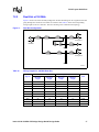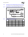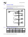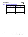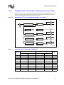
1
Intel® 31154 133 MHz PCI Bridge
Design Guide
Design Guide
April 2004
Order Number: 278944-001
INFORMATION IN THIS DOCUMENT IS PROVIDED IN CONNECTION WITH INTEL ® PRODUCTS. EXCEPT AS PROVIDED IN INTEL’S TERMS
AND CONDITIONS OF SALE FOR SUCH PRODUCTS, INTEL ASSUMES NO LIABILITY WHATSOEVER, AND INTEL DISCLAIMS ANY EXPRESS
OR IMPLIED WARRANTY RELATING TO SALE AND/OR USE OF INTEL PRODUCTS, INCLUDING LIABILITY OR WARRANTIES RELATING TO
FITNESS FOR A PARTICULAR PURPOSE, MERCHANTABILITY, OR INFRINGEMENT OF ANY PATENT, COPYRIGHT, OR OTHER
INTELLECTUAL PROPERTY RIGHT.
Intel Corporation may have patents or pending patent applications, trademarks, copyrights, or other intellectual property rights that relate to the
presented subject matter. The furnishing of documents and other materials and information does not provide any license, express or implied, by
estoppel or otherwise, to any such patents, trademarks, copyrights, or other intellectual property rights.
Intel products are not intended for use in medical, life saving, life sustaining, critical control or safety systems, or in nuclear facility applications.
Intel may make changes to specifications and product descriptions at any time, without notice.
Designers must not rely on the absence or characteristics of any features or instructions marked “reserved” or “undefined.” Intel reserves these for
future definition and shall have no responsibility whatsoever for conflicts or incompatibilities arising from future changes to them.
The Intel® 31154 133 MHz PCI Bridge may contain design defects or errors known as errata which may cause the product to deviate from published
specifications. Current characterized errata are available on request.
This Design Guide as well as the software described in it is furnished under license and may only be used or copied in accordance with the terms of
the license. The information in this manual is furnished for informational use only, is subject to change without notice, and should not be construed as
a commitment by Intel Corporation. Intel Corporation assumes no responsibility or liability for any errors or inaccuracies that may appear in this
document or any software that may be provided in association with this document.
Except as permitted by such license, no part of this document may be reproduced, stored in a retrieval system, or transmitted in any form or by any
means without the express written consent of Intel Corporation.
Contact your local Intel sales office or your distributor to obtain the latest specifications and before placing your product order.
Copies of documents which have an ordering number and are referenced in this document, or other Intel literature may be obtained by calling
1-800-548-4725 or by visiting Intel's website at http://www.intel.com.
AnyPoint, AppChoice, BoardWatch, BunnyPeople, CablePort, Celeron, Chips, CT Media, Dialogic, DM3, EtherExpress, ETOX, FlashFile, i386, i486,
i960, iCOMP, InstantIP, Intel, Intel Centrino, Intel logo, Intel386, Intel486, Intel740, IntelDX2, IntelDX4, IntelSX2, Intel Create & Share, Intel GigaBlade,
Intel InBusiness, Intel Inside, Intel Inside logo, Intel NetBurst, Intel NetMerge, Intel NetStructure, Intel Play, Intel Play logo, Intel SingleDriver, Intel
SpeedStep, Intel StrataFlash, Intel TeamStation, Intel Xeon, Intel XScale, IPLink, Itanium, MCS, MMX, MMX logo, Optimizer logo, OverDrive,
Paragon, PC Dads, PC Parents, PDCharm, Pentium, Pentium II Xeon, Pentium III Xeon, Performance at Your Command, RemoteExpress, SmartDie,
Solutions960, Sound Mark, StorageExpress, The Computer Inside, The Journey Inside, TokenExpress, VoiceBrick, VTune, and Xircom are
trademarks or registered trademarks of Intel Corporation or its subsidiaries in the United States and other countries.
*Other names and brands may be claimed as the property of others.
Copyright © 2004, Intel Corporation
2
Intel® 31154 133 MHz PCI Bridge Design Guide
Contents
Contents
1
About This Document ......................................................................................................................7
1.1
2
Introduction ...................................................................................................................................... 9
2.1
2.2
2.3
2.4
3
Terminology and Definitions ................................................................................................. 7
Product Overview .................................................................................................................9
Features List ....................................................................................................................... 10
Related External Specifications ..........................................................................................11
References ......................................................................................................................... 11
Package Information......................................................................................................................13
3.1
Total Signal Count .............................................................................................................. 17
4
Terminations ..................................................................................................................................19
5
PCI/PCI-X Interface ....................................................................................................................... 29
5.1
5.2
5.3
5.4
5.5
5.6
6
Routing Guidelines ........................................................................................................................ 35
6.1
6.2
6.3
6.4
7
PCI/PCI-X Voltage Levels................................................................................................... 29
Interrupt Routing ................................................................................................................. 29
IDSEL Lines ........................................................................................................................ 30
5.3.1 Primary IDSEL Line ............................................................................................... 30
5.3.2 Secondary IDSEL Lines......................................................................................... 30
5.3.3 Secondary IDSEL Masking .................................................................................... 31
5.3.4 Secondary Clock Control ....................................................................................... 31
CompactPCI* Hot Swap Mode Select ................................................................................ 31
Opaque Memory Region Enable ........................................................................................ 31
PCI-X Initialization Clocking Modes .................................................................................... 32
5.6.1 Primary PCI Clocking Mode................................................................................... 32
5.6.2 Secondary PCI Clocking Mode ..............................................................................32
5.6.3 Primary-to-Secondary Frequency Limits................................................................ 34
Crosstalk ............................................................................................................................. 36
EMI Considerations ............................................................................................................ 37
Power Distribution and Decoupling.....................................................................................38
6.3.1 Decoupling Recommendations ..............................................................................38
Trace Impedance ................................................................................................................ 39
PCI-X Layout Guidelines ...............................................................................................................41
7.1
7.2
PCI Clock Layout Guidelines .............................................................................................. 42
PCI-X Topology Layout Guidelines.....................................................................................44
7.2.1 Single Slot at 133 MHz ..........................................................................................45
7.2.1.1 Intel® 31154 133 MHz PCI Bridge Embedded Application at 133 MHz . 46
7.2.2 Dual-Slot at 100 MHz............................................................................................. 47
7.2.2.1 Embedded Intel® 31154 133 MHz PCI Bridge Application at 100 MHz . 48
7.2.3 Quad-Slots at 66 MHz ........................................................................................... 49
7.2.3.1 Embedded Intel® 31154 133 MHz PCI Bridge Application at 66 MHz ... 51
7.2.4 PCI-X at 33 MHz .................................................................................................... 52
7.2.4.1 Embedded PCI-X Specification PICMG 1.2 Overview ........................... 52
Intel® 31154 133 MHz PCI Bridge Design Guide
3
Contents
7.2.4.2
8
PICMG 1.2 System Overview ................................................................ 52
Power Considerations ................................................................................................................... 57
8.1
8.2
Analog Power Pins ............................................................................................................. 57
Power Sequencing.............................................................................................................. 58
9
Customer Reference Board........................................................................................................... 59
10
Debug Connectors and Logic Analyzer Connectivity .................................................................... 61
10.1
Probing PCI-X Signals ........................................................................................................ 61
11
Thermal Solutions.......................................................................................................................... 69
12
References .................................................................................................................................... 71
12.1
Related Documents ............................................................................................................ 71
Figures
1
2
3
4
5
6
7
8
9
10
11
12
13
14
15
16
17
18
19
20
21
Intel® 31154 133 MHz PCI Bridge Applications............................................................................ 9
Intel® 31154 133 MHz PCI Bridge Package ............................................................................... 14
Intel® 31154 133 MHz PCI Bridge Ball Map—Top View, Left Side ............................................ 15
Intel® 31154 133 MHz PCI Bridge Ball Map—Top View, Right Side .......................................... 16
IDSEL Mapping .......................................................................................................................... 30
Crosstalk Effects on Trace Distance and Height ........................................................................ 36
PCB Ground Layout Around Connectors ................................................................................... 37
PCI Clock Distribution and Matching Requirements................................................................... 43
Single-Slot Point-to-Point Topology............................................................................................ 45
Embedded Intel® 31154 133 MHz PCI Bridge Design 133 MHz PCI-X Layout.......................... 46
Dual-Slot Configuration .............................................................................................................. 47
Embedded Intel® 31154 133 MHz PCI Bridge Design 100 MHz PCI-X Layout.......................... 48
Quad-Slots 66 MHz Topology .................................................................................................... 49
Embedded Intel® 31154 133 MHz PCI Bridge Wiring for 66 MHz.............................................. 51
An Example of an ePCI-X System.............................................................................................. 53
PCI-X Data Bus PICMG 1.2 Style Backplane............................................................................. 54
PCI-X Clock PICMG 1.2 Style Backplane .................................................................................. 55
P_VCCA Filter ............................................................................................................................ 57
S_VCCA Filter ............................................................................................................................ 57
PVIO Voltage Protection Diode .................................................................................................. 58
Intel® IQ31154 Customer Reference Board Block Diagram....................................................... 59
Tables
1
2
3
4
5
6
7
8
4
Terminology and Definition ........................................................................................................... 7
PCI-to-PCI Bridge Configurations................................................................................................. 9
Features List ............................................................................................................................... 10
Total Signal Count ...................................................................................................................... 17
Pull-Up/Pull-Down Terminations................................................................................................. 19
PCI/PCI-X Voltage Levels .......................................................................................................... 29
HS_FREQ Encoding................................................................................................................... 31
PCI-X Clocking Modes ............................................................................................................... 33
Intel® 31154 133 MHz PCI Bridge Design Guide
Contents
9
10
11
12
13
14
15
16
17
18
19
20
21
22
23
24
25
26
27
28
29
30
31
Secondary Bus Frequency Initialization...................................................................................... 33
PCI-X Initialization Pattern.......................................................................................................... 34
Intel® 31154 133 MHz PCI Bridge Decoupling Recommendations ............................................ 38
Add-in Card Routing Parameters................................................................................................ 41
PCI-X Slot Guidelines ................................................................................................................. 44
Wiring Lengths for 133 MHz Slot ................................................................................................ 45
Wiring Lengths for Embedded 133 MHz Design.........................................................................46
Wiring Lengths for 100 MHz Dual-Slot ....................................................................................... 47
Wiring Lengths for Embedded 100 MHz Design.........................................................................48
Wiring Lengths for 66 MHz Quad-Slot ........................................................................................ 49
Wiring Lengths for Embedded 66 MHz Design........................................................................... 51
Wiring Lengths for PICMG 1.2 Backplane .................................................................................. 54
PCI-X Clock Wiring Lengths for PICMG Backplane ................................................................... 55
Customer Reference Board Stackup ..........................................................................................60
Logic Analyzer Pod 1 .................................................................................................................. 62
Logic Analyzer Pod 2 .................................................................................................................. 63
Logic Analyzer Pod 3 .................................................................................................................. 64
Logic Analyzer Pod 4 .................................................................................................................. 65
Logic Analyzer Pod 5 .................................................................................................................. 66
Logic Analyzer Pod 6 .................................................................................................................. 67
Operational Power ......................................................................................................................69
Design Reference Material ......................................................................................................... 71
Intel® Related Documentation .................................................................................................... 71
Intel® 31154 133 MHz PCI Bridge Design Guide
5
Contents
Revision History
6
Date
Revision
April 2004
001
Description
Initial release
Intel® 31154 133 MHz PCI Bridge Design Guide
About This Document
1
About This Document
This document provides layout information and guidelines for designing platform or add-in board
applications with the Intel® 31154 133 MHz PCI Bridge.
This document is intended to be used as a guideline only. Intel recommends that you employ bestknown design practices with board-level simulation, signal-integrity testing, and validation for a
robust design. Please note that this design guide focuses on specific design considerations for the
31154 Bridge and is not intended to be an all-inclusive list of all good design practices. Use this
guide as a starting point, and use empirical data to optimize your particular design.
1.1
Terminology and Definitions
Table 1.
Terminology and Definition (Sheet 1 of 2)
Term
31154
Definition
®
Intel 31154 133 MHz PCI Bridge
Stripline in a PCB is composed of the
conductor inserted in a dielectric with GND
planes to the top and bottom, as shown in the
cross-section diagram at left.
Stripline
NOTE: An easy way to distinguish stripline
from microstrip is that you need to
strip away layers of the board to view
the trace on stripline.
Microstrip in a PCB is composed of the
conductor on the top layer above the
dielectric with a ground plane below, as
shown in the cross-section diagram at left.
Microstrip
Prepreg
Core
Prepreg is material used for the lamination process of manufacturing PCBs. It consists of a
layer of epoxy material that is placed between two cores. This layer melts into epoxy when
heated and forms around adjacent traces.
Core material is used for the lamination process of manufacturing PCBs. This material is twosided laminate with copper on each side. The core is an internal layer that is etched.
Layer 1: copper
Prepreg
Layer 2: GND
Core
PCB
Layer 3: VCC
Prepreg
Layer 4: copper
Printed circuit board: An example PCB
manufacturing process consists of the
following steps:
• A PCB consists of alternating layers of
core and prepreg stacked.
• The finished PCB is heated and cured.
• The via holes are drilled.
• Plating covers holes and outer surfaces.
• Etching removes unwanted copper.
Example of a cross-section of
a four-layer stack
Intel® 31154 133 MHz PCI Bridge Design Guide Design Guide
• The PCB is tinned, coated with solder
mask, and silk-screened.
7
About This Document
Table 1.
Terminology and Definition (Sheet 2 of 2)
Term
Definition
An aggressor network is a network that transmits a coupled signal to another network.
Zo
Aggressor
Zo
Victim Network
Zo
Zo
Aggressor Network
B3337-01
Victim
A network that receives a coupled cross-talk signal from another network is a called the victim
network.
Network
A network is the trace of a PCB that completes an electrical connection between two or more
components.
Stub
ISI
A stub is a branch from a trunk terminating at the pad of an agent.
Inter-Symbol Interference (ISI) occurs when a transition that has not been completely
dissipated interferes with a signal being transmitted down a transmission line. ISI can impact
both timing and signal integrity. It is dependent on frequency, time delay of the line, and the
refection coefficient at the driver and receiver. Examples of ISI patterns that can be used in
testing at the maximum allowable frequencies are the sequences shown below:
0101 0101 0101 0101
0011 0011 0011 0011
000 1110 0011 1000 1111
Device
Downstream
Upstream
SHB
ePCI-X
CRB
A device is a component of a PCI system that connects to a PCI bus. As defined by PCI 2.3,
a device can be a single-function or a multi-function device.
A transaction that targets the secondary side of the bridge is a downstream transaction.
A transaction that targets the primary side of the bridge is an upstream transaction.
SHB is a system host board in a PICMIG 1.2 backplane. The removable CPU board provides
clocks and arbitration signals as well as an optional ATX power supply control.
Embedded PCI-X specification
Customer Reference Board
§§
8
Intel® 31154 133 MHz PCI Bridge Design Guide Design Guide
Introduction
2
Introduction
2.1
Product Overview
The Intel® 31154 133 MHz PCI Bridge (called hereafter the “31154”) is a PCI component that
functions as a highly concurrent, low-latency transparent bridge between two PCI buses. The
31154 can operate as a PCI-to-PCI bridge in the configurations shown in Table 2.
Table 2.
PCI-to-PCI Bridge Configurations
Primary Bus Interface
Secondary Bus Interface
PCI 2.3
PCI 2.3
PCI 2.3
PCI-X
PCI-X
PCI 2.3
PCI-X
PCI-X
The 31154 is used on motherboards to provide additional I/O expansion slots. It is also used on PCI
add-in cards to mitigate the restrictive electrical loading constraints imposed on an expansion slot,
enabling multiple conventional PCI or multiple PCI-X devices to reside on a single PCI I/O
adapter. The 31154 block diagram in Figure 1 indicates potential 31154 applications for a range of
PCI bus speeds.
Intel® 31154 133 MHz PCI Bridge Applications
Multi PCI-X
Devices
High-End
Application
PCI-X Bus 133 MHz Slot
Legacy
66 MHz
PCI-X Bus 100 MHz Slots
Legacy
33 MHz
PCI-X Bus 66 MHz Slots
PCI-X Bus
Figure 1.
CPU Host
Intel® 31154 133 MHz PCI Bridge Design Guide Design Guide
9
Introduction
The 31154 has additional hardware support for CompactPCI* Hot Swap and Redundant System
Slot via queue flush, arbiter lock, and clock output tristating.
The 31154 supports any combination of 32-bit and 64-bit data transfers on its primary and
secondary bus interfaces. The 31154 is 33/66 MHz capable in conventional PCI mode, and can run
at 66 MHz, 100 MHz, or 133 MHz when operating in PCI-X mode, depending upon its
surrounding environment.
2.2
Features List
Table 3.
Features List
• PCI bus interfaces (2):
• Secondary bus arbitration:
— PCI Local Bus Specification,
Revision 2.3 compliant
— Internal arbiter supports nine agents in
addition to the 31154.
— PCI-to-PCI Bridge Architecture
Specification, Revision 1.2 compliant
— Internal arbiter can be disabled.
— PCI Bus Power Management
Interface Specification, Revision 1.1
compliant
— PCI-X Addendum to the PCI Local
Bus Specification, Revision 1.0b
compliant
— External SROM support
— Vital Products Data (VPD) support
— 64-bit initiator/target capable
— 64-bit addressing
• Hardware support for dual-host cPCI
configurations
• Compact PCI Hot Swap Specification,
Revision 2.1 R2.0 support
• Secondary clock generation with 10 clock
outputs
— Optimized for PCI-X mode
— Bus parking on bridge or last master
• Improved buffer architecture:
— 8 KBytes data buffers in each
direction
— Improved level of concurrency:
Up to nine outstanding transactions on
each bus simultaneously
• Scalability and flexibility:
— Conventional PCI 32/64-bit
33/66 MHz, 3.3 V
— 5 V tolerant inputs
— PCI-X 32/64-bit 66/100/133 MHz,
3.3 V
• JTAG interface
• GPIO interface:
— Allows simple software-controlled
signaling protocols
10
Intel® 31154 133 MHz PCI Bridge Design Guide Design Guide
Introduction
2.3
Related External Specifications
•
•
•
•
•
•
2.4
PCI Local Bus Specification, Revision 2.3
PCI-to-PCI Bridge Architecture Specification, Revision 1.1
PCI Bus Power Management Interface Specification, Revision 1.1
Compact PCI Hot Swap Specification, Revision 2.1 R2.0
PCI-X Addendum to the PCI Local Bus Specification, Revision 1.1
Embedded PCI-X Specification PICMG 1.2 R1.0
References
This section lists references that can be useful with a 31154 application. These documents are
available on the Intel Developer website (http://developer.intel.com):
•
•
•
•
•
Intel® 31154 133 MHz PCI Bridge Datasheet (278821)
Intel® 31154 133 MHz PCI Bridge Developer’s Manual (278848)
Intel® 31154 133 MHz PCI Bridge Specification Update (300826)
Intel® 31154 133 MHz PCI Bridge Design Checklist (300959)
Intel® 31154 133 MHz PCI Bridge Evaluation Board Schematics (278839)
§§
Intel® 31154 133 MHz PCI Bridge Design Guide Design Guide
11
Introduction
THIS PAGE INTENTIONALLY LEFT BLANK
12
Intel® 31154 133 MHz PCI Bridge Design Guide Design Guide
Package Information
Package Information
3
The Intel® 31154 133 MHz PCI Bridge is offered in a 421-lead PBGA package. The mechanical
dimensions for this package are provided in Figure 2 on page 14.
Figure 3 on page 15 and Figure 4 on page 16 show the 421-lead PBGA, mapped by pin function.
These figures are helpful in placing components around the 31154 for the layout of a PCB. To
simplify routing and minimize the number of cross traces, keep this layout in mind when placing
components on your board. The signals, by design, are located on the PBGA package to simplify
signal routing and system implementation. Figure 3 shows the left side of the 31154 ball map, and
Figure 4 shows the right side of the ball map.
Intel® 31154 133 MHz PCI Bridge Design Guide Design Guide
13
Package Information
Figure 2.
Intel® 31154 133 MHz PCI Bridge Package
Notes:
1. All dimensions and tolerances conform to ANSI Y14.5M-1982.
2
3
Dimension is measured at the maximum solder ball
diameter, parallel to primary datum
Ø
2
Primary datum
and seating plane are defined by the
spherical crowns of the solder balls.
Ø 0.30 S C A S
0.90
0.60
22
23
20
21
18
19
17
16 14 12 10
8
6
15 13 11
9
7
5
B S
1.27
0.127 A
31.00 ± 0.10
26.00 ± 0.20
SEE DETAIL "A"
PIN #1
CORNER
2
3
1
A
B
C
D
E
F
G
H
J
K
L
M
N
P
R
T
U
V
W
Y
AA
AB
AC
4. All dimensions, unless otherwise specified, are in millimeters.
//
4
1.53 REF
1.53 REF
-B-
1.27
1.27
BOTTOM VIEW
31.00 ± 0.10
(22.10 REF)
26.00 ± 0.20
0.127 A
3 X Ø1.00 THRU
45˚ CHAMFER
4 PLACES
(22.10 REF)
PIN #1 CORNER
NO RADIUS
TOP VIEW
Au GATE
1.70
2.38 ± 0.21
1.17 ± 0.05
30˚
90.0˚
//
0.15 C
0.15
0.61 ± 0.06
PIN #1 I.D. (SHINY)
1.0 DIA. X 0.15 DEPTH
9.0 X 9.0 FROM CENTER LINE
-C-
0.60 ± 0.10
3
SIDE VIEW
SEATING PLANE
DETAIL "A"
NOT TO SCALE
B1290-01
14
Intel® 31154 133 MHz PCI Bridge Design Guide Design Guide
Package Information
Figure 3.
Intel® 31154 133 MHz PCI Bridge Ball Map—Top View, Left Side
1
2
3
P_
P_
ACK64# AD56
4
5
6
7
8
9
10
11
12
P_
AD60
P_
CBE4#
VSS
P_
CBE7#
VCCP
P_
PAR64
VSS
VSS
VCCP
P_
AD63
P_
CBE6#
A
VSS
B
P_
AD43
VSS
P_
AD54
P_
SERR#
P_
AD49
P_
AD50
P_
AD52
P_
AD55
P_
AD57
P_
AD59
C
SCAN_
EN
P_
AD48
VSS
P_
STOP#
VCCP
S_CLK
OEN3
P_
AD53
P_
PERR#
P_
AD58
P_
AD61
D
S_CLK
OEN2
P_
AD47
QE
VSS
VCCP
P_
AD51
VCCP
VSS
VCC
P_
AD62
E
P_
AD38
S_CLK
OEN1
P_
AD45
VCCP
R_REF
VSS
HS_
LED_
OUT
F
VSS
P_
AD42
P_
AD44
P_
AD46
VSS
VCC
VSS
G
P_
AD36
S_CLK
OEN0
P_
AD41
VCCP
HS_
SM
VSS
H
P_
AD35
P_
AD39
P_
AD40
VSS
P_
M66EN
VCC
J
P_
AD33
P_
AD34
P_
AD37
VCC
SR_
CLK
VSS
K
VSS
S_
AD34
S_
AD33
S_
AD32
VSS
VCC
L
P_
AD32
S_
AD36
S_
AD35
VCC
M
VCCP
S_
AD39
S_
AD38
N
VSS
S_
AD41
P
VSS
R
HS_
HS_
LSTAT ENUM#
VCC
VSS
VSS
P_
P_
CBE5# REQ64#
VCC
VSS
S_TRI
HS_
STATE FREQ0
VCC
VSS
VSS
VSS
SR_CS
VSS
VSS
VSS
VSS
SR_DO
VSS
VSS
VSS
S_
AD40
VCC
SR_DI
VSS
VSS
VSS
S_
AD47
S_
AD45
S_
AD43
VSS
VSS
VSS
VSS
VSS
S_
AD37
S_
AD49
S_
AD48
VCC
S_
GNT7#
VCC
T
S_VIO
S_
AD51
S_
AD50
VSS
S_
REQ7#
VSS
U
S_
AD42
S_
AD53
S_
AD52
VCCP
S_
GNT6#
VCC
V
VSS
S_
AD55
S_MAX
100
S_
AD54
VSS
VSS
VCC
VSS
VCC
VSS
W
S_
AD44
S_
S_CLK
VCCP
REQ2# STABLE
S_
REQ6#
VSS
VSS
VSS
VSS
VSS
VSS
VSS
Y
S_
AD46
S_
GNT2#
S_
AD56
VCCP
S_
AD57
VCCP
VSS
VCC
S_
CBE7#
VCC
VSS
AA
NC
S_
REQ1#
VSS
S_
TMODE
2
AD58
S_
AD59
S_
S_
S_
AD61 ACK64# AD00
S_
S_
PAR64 CBE5#
AB
S_
GNT1#
VSS
S_
S_
S_
REQ3# GNT4# REQ4#
S_
AD60
S_
AD62
S_
AD63
S_
AD01
S_
CBE6#
S_
AD04
S_
CBE0#
AC
VSS
VCCP
S_
S_
S_
REQ5# GNT5# GNT3#
VSS
CRS
TEN
S_
CBE4#
S_
AD02
VSS
S_
AD03
VCCP
6
7
8
9
10
11
12
1
2
3
VSS
4
5
S_
AD06
B2240-01
Intel® 31154 133 MHz PCI Bridge Design Guide Design Guide
15
Package Information
Figure 4.
Intel® 31154 133 MHz PCI Bridge Ball Map—Top View, Right Side
13
14
P_
CBE0#
VSS
P_
P_
P_
CBE3# IRDY# FRAME#
P_
AD00
P_
AD02
P_
TRDY#
P_
AD05
P_
AD01
MT0#
P_
AD03
VCC
P_
CBE2#
VCC
HS_
FREQ1
VSS
VSS
15
18
19
20
21
22
23
VSS
P_
AD04
P_
AD07
P_
VCCA
VCCP
VSS
A
P_
AD08
P_
CBE1#
P_
IDSEL
P_
AD15
P_
REQ#
VSS
TDO
B
P_
AD06
P_
AD09
P_
PAR
P_
AD10
P_
GNT#
VSS
TDI
TRST#
C
VSS
VCCP
P_
AD11
VCCP
VSS
P_DEV
SEL#
TMS
P_
AD22
D
NT_
GPIO0 GPIO1
MASK#
VSS
GPIO2
VCCP
P_
CLK
P_
RST#
P_
AD24
E
VSS
VSS
VSS
P_
AD13
TCK
P_
AD12
VSS
F
VCC
VSS
VCCP
P_
AD16
P_
AD14
P_
AD26
G
VSS
VCC
VSS
P_
AD18
P_
AD17
P_VIO
H
S_
S_
CLKO0 CLKO2
VCC
P_
AD20
P_
AD19
P_
AD31
J
VCC
16
17
VCC
VSS
VSS
S_
S_
CLKO1 CLKO4
P_
AD25
P_
AD23
P_
AD21
VSS
K
VSS
VSS
S_
CLKO3
VCC
P_
AD28
P_
AD27
VSS
L
VSS
VSS
S_
CLKO5
VSS
P_
AD30
P_
AD29
S_
AD27
M
VSS
VSS
S_
CLKO6
VCC
S_
AD30
S_
AD31
S_
AD25
N
VSS
VSS
S_BRG
S_
CLKO CLK07
S_
AD26
S_
AD28
S_
AD29
VSS
P
S_
S_
M66EN CLKO8
VCC
S_
AD22
S_
AD24
S_PCIX
CAP
R
S_
GNT8#
VCC
VCC
VSS
S_ARB
_DIS
ABLE
S_
AD20
S_
AD23
T
VSS
S_
GCLK
OEN
VCCP
S_
AD18
S_
AD19
S_
RST#
U
VCC
VSS
S_
AD14
S_
AD16
S_
AD17
VSS
V
VSS
VCCP
S_
S_
TMODE
0
AD15
AD21
W
VCCP
VSS
TMODE DEV_ TMODE
1
3
64BIT#
Y
S_
OPAQUE
_EN
GNT0#
S_
AD13
VCC
GPIO3 GPIO5
VCC
VSS
S_
GPIO4 GPIO6 GPIO7
REQ8#
VCC
S_
TRDY#
VCC
S_
S_
S_
AD07 FRAME# CBE3#
S_
S_
REQ64# CBE2#
VSS
VCCP
S_
AD10
S_
PAR
S_
AD09
S_
S_
CBE1# PERR#
S_
AD11
S_
AD12
S_
S_
SERR# STOP#
VSS
VSS
S_
AD05
VCCP
S_
AD08
VSS
S_
IRDY#
MT1#
13
14
15
16
17
18
19
20
VSS
S_
VCCA
RSRV0
S_
REQ0#
AA
VSS
S_
CLKI
AB
VSS
AC
S_
IDSEL_
DEVSEL# MASK
21
22
23
B2241-01
16
Intel® 31154 133 MHz PCI Bridge Design Guide Design Guide
Package Information
3.1
Total Signal Count
Table 4.
Total Signal Count
Interface
Signals
PCI bus interface
112
PCI 64-bit extensions
78
Clock and reset
20
JTAG
12
Serial ROM interface
4
CompactPCI* Hot Swap
6
Hardware strap
5
Miscellaneous
17
Total
254
§§
Intel® 31154 133 MHz PCI Bridge Design Guide Design Guide
17
Package Information
THIS PAGE INTENTIONALLY LEFT BLANK
18
Intel® 31154 133 MHz PCI Bridge Design Guide Design Guide
Terminations
4
Terminations
This chapter details all the recommended Intel® 31154 133 MHz PCI Bridge terminations required
for the different operating modes.
The chapter provides the recommended pull-up and pull-down terminations for a 31154 layout.
Table 5 lists these 31154 termination values. Note that for motherboards, the PCI Local Bus
Specification, Revision 2.3 requires that the PCI signals provide the termination resistors.
Table 5.
Pull-Up/Pull-Down Terminations (Sheet 1 of 9)
Signal
Pull-Up/Pull-Down or Termination (See Note 1)
Comments
PCI Reset
P_RST#
Connect to bus RST# signal on primary PCI bus.
S_RST#
Connect to bus RST# signal on secondary PCI
bus.
Primary PCI Signals
P_AD[31:0]
Connect to primary PCI bus AD[31:0].
For 64-bit primary PCI bus:
P_AD[63:32]
• Connect to the AD[63:32] bits of the primary
PCI bus.
For 32 bit Primary PCI Bus:
• Pull up through individual external resistors
(see Note 2 and Note 3).
P_CBE[3:0]
Connect to the CBE[3:0}# bits of the primary PCI
bus.
For 64-bit primary PCI bus:
P_CBE[7:4]#
• Connect to the CBE[7:4]# bits of the primary
PCI bus.
For 32-bit primary PCI Bus:
• Pull up through individual external resistors
(see Note 2 and Note 3).
P_FRAME#
Connect to FRAME# of the primary PCI bus.
P_DEVSEL#
Connect to DEVSEL# of the primary PCI bus.
P_IRDY#
Connect to IRDY# of the primary PCI bus.
P_TRDY#
Connect to TRDY# of the primary PCI bus.
P_STOP#
Connect to STOP# of the primary PCI bus.
NOTES:
1. The recommended value for pull-up resistors for PCI applications is 5.6 KΩ (note that the minimum value for PCI 3.3 V
signaling R MIN = 2.42 KΩ, RTYP = 8.2 KΩ, as per the PCI Local Bus Specification, Revision 2.3, section 4.3.3).
2. The recommended value for pull-up resistors for PCI-X applications is 8.2 KΩ. For PCI-X, the minimum pull-up resistor value
is 5 KΩ, as per the PCI-X Addendum to the PCI Local Bus Specification, Revision 1.0b, section 9.7.
3. For plug-in card implementations, the pull-up must be on the motherboard.
4. Connect PVIO and SVIO pull-up resistors to 5 V or 3.3 V power supply through an external resistor—25 Ω (5 V) or
0 Ω (3.3 V), depending on the signaling level of the primary/secondary PCI bus. Refer to the power-sequencing guidelines in
Section 8.2 on page 58.
Intel® 31154 133 MHz PCI Bridge Design Guide Design Guide
19
Terminations
Table 5.
Pull-Up/Pull-Down Terminations (Sheet 2 of 9)
Signal
Pull-Up/Pull-Down or Termination (See Note 1)
P_GNT#
Connect to GNT# of the primary PCI bus.
P_IDSEL#
Connect to one of the AD lines of the primary PCI
bus or to the IDSEL# signal of the PCI edge
connector (for add-in card applications).
P_M66EN
Connect to the M66EN signal of the primary PCI
bus of the PCI add-in card finger.
P_PAR
Connect to PAR of the primary PCI bus.
P_PAR64
Connect to PERR# of the primary PCI bus.
P_PERR#
Connect to PERR# of the primary PCI bus.
P_REQ#
Connect to one of the PCI bus request signals of
the primary PCI bus.
P_SERR#
Connect to SERR# of the primary PCI bus.
Comments
Refer to Section 5.3, “IDSEL Lines” on page 30 for
more details.
Secondary PCI Signals
S_AD[63:32]
Pull up to VCC33 through external 8.2 KΩ
resistors.
S_CBE[7:4]#
Pull up to VCC33 through external 8.2 KΩ
resistors.
S_REQ64#
Pull up to VCC33 through external 8.2 KΩ
resistors.
S_ACK64#
Pull up to VCC33 through external 8.2 KΩ
resistors.
S_FRAME#,
S_IRDY#,
S_TRDY#,
S_STOP#,
S_DEVSEL#,
S_PERR#,
S_SERR#
Pull up to VCC33 voltage through external 8.2 KΩ
resistors.
S_REQ[8:1]#,
S_REQ0#/BR_GNT#,
S_GNT0#/BR_REQ#
Pull up to VCC33 voltage through external 8.2 KΩ
resistors.
Pull-up for both internal and external arbiter mode.
Secondary GNT#
S_GNT1#,
S_GNT2#,
S_GNT3#,
S_GNT4#,
S_GNT5#,
S_GNT6#,
S_GNT7#,
S_GNT8#
Connect to GNT# input of the PCI devices on the
secondary PCI bus.
NC when not used.
NOTES:
1. The recommended value for pull-up resistors for PCI applications is 5.6 KΩ (note that the minimum value for PCI 3.3 V
signaling RMIN = 2.42 KΩ, RTYP = 8.2 KΩ, as per the PCI Local Bus Specification, Revision 2.3, section 4.3.3).
2. The recommended value for pull-up resistors for PCI-X applications is 8.2 KΩ. For PCI-X, the minimum pull-up resistor value
is 5 KΩ, as per the PCI-X Addendum to the PCI Local Bus Specification, Revision 1.0b, section 9.7.
3. For plug-in card implementations, the pull-up must be on the motherboard.
4. Connect PVIO and SVIO pull-up resistors to 5 V or 3.3 V power supply through an external resistor—25 Ω (5 V) or
0 Ω (3.3 V), depending on the signaling level of the primary/secondary PCI bus. Refer to the power-sequencing guidelines in
Section 8.2 on page 58.
20
Intel® 31154 133 MHz PCI Bridge Design Guide Design Guide
Terminations
Table 5.
Signal
S_AD[31:17]
Pull-Up/Pull-Down Terminations (Sheet 3 of 9)
Pull-Up/Pull-Down or Termination (See Note 1)
Comments
These signals can be used as IDSEL lines and are
connected to IDSEL of the secondary PCI bus
through an external series coupling resistor (a
resistor of 2 KΩ is used on the customer reference
board).
PCI Clocks
P_CLK
Connect to the PCI clock on the primary PCI bus.
S_BRGCLKO
When the internal clock of the 31154 is used,
connect to S_CLKI through a 33.2 Ω series
resistor.
NC when external clock is used.
• All S_CLKO[8:0] and S_BRGCLKO must
match in length.
• When there are PCI slots in the design,
S_BRGCLKO must be 3" longer to
compensate for the 2.5" trace length from the
connector to the PCI device on a PCI add-in
card.
• These clocks can be disabled by strapping the
S_CLKOEN[3:0] during reset.
S_CLKO[8:0]
When the internal clock of the 31154 is used,
connect to the PCI clock input of the secondary
PCI devices through a 33.2 Ω series resistor.
Each clock can be connected to only one PCI
device.
• All S_CLKO[8:0] and S_BRGCLKO must
match in length.
• For asynchronous mode, there is no maximum
skew between P_CLK and S_CLKI.
NOTE: These clocks can be disabled by
strapping the S_CLKOEN[3:0] during
reset.
• When using the internal clock, refer to
S_BRGCLKO (above) for additional
information.
S_CLKI
S_CLKSTABLE
When the internal clock of the 31154 is used,
connect to S_BRGCLKO.
• When using an external clock source, all
secondary clocks must have matching length.
When an external clock is used, connect to
external clock source.
• When using PCI slots in the design,
S_BRGCLKO must be 3" longer to
compensate for the 2.5" trace length from the
connector to the PCI device on a PCI add-in
card.
When the internal clock of the 31154 is used,
S_CLKSTABLE must be tied high to VCC33
through an external 8.2 KΩ resistor.
When an external clock source is used, connect to
logic that outputs high after the secondary clocks
are stable.
NOTES:
1. The recommended value for pull-up resistors for PCI applications is 5.6 KΩ (note that the minimum value for PCI 3.3 V
signaling R MIN = 2.42 KΩ, RTYP = 8.2 KΩ, as per the PCI Local Bus Specification, Revision 2.3, section 4.3.3).
2. The recommended value for pull-up resistors for PCI-X applications is 8.2 KΩ. For PCI-X, the minimum pull-up resistor value
is 5 KΩ, as per the PCI-X Addendum to the PCI Local Bus Specification, Revision 1.0b, section 9.7.
3. For plug-in card implementations, the pull-up must be on the motherboard.
4. Connect PVIO and SVIO pull-up resistors to 5 V or 3.3 V power supply through an external resistor—25 Ω (5 V) or
0 Ω (3.3 V), depending on the signaling level of the primary/secondary PCI bus. Refer to the power-sequencing guidelines in
Section 8.2 on page 58.
Intel® 31154 133 MHz PCI Bridge Design Guide Design Guide
21
Terminations
Table 5.
Signal
Pull-Up/Pull-Down Terminations (Sheet 4 of 9)
Pull-Up/Pull-Down or Termination (See Note 1)
Comments
When the internal clock of the 31154 is used, pull
high to VCC33 through an external 8.2 KΩ resistor.
S_GCLKOEN
When an external clock source is used, tie to GND
through a 330 Ω external resistor. All secondary
clock outputs (S_CLKO[8:0] and S_BRGCLKO)
asynchronously tristate.
When an external clock source is used, tie
S_CLKOEN[3:0] to a stable value. Refer to
S_CLKOEN[3:0], below.
These are strapping pins to enable or tristate
S_CLKO[8:0] after reset.
S_CLKOEN[3:0]
• To enable all S_CLKO[8:0], pull each
S_CLKOEN[3:0] pin to 3.3 V through an
external 8.2 KΩ resistor.
NOTE: This strapping is meaningful only when
S_GCLKOEN is pulled high.
When external clocks are used, tie S_GCLKOEN
low and tie S_CLKOEN[3:0] to some stable value
(0000b, for example).
• To selectively disable some of the
S_CLKO[8:0], refer to 31154 Control
Register 2, bits[8:0].
Hot Swap
For Hot Swap:
HS_ENUM#
• Connect the interrupt input pin to the host.
When not using Hot Swap:
• NC (there is a weak internal pull-up).
For Hot Swap:
HS_LSTAT
• Connect to cPCI ejector switch.
When not using Hot Swap:
• Tie low to GND.
For Hot Swap:
HS_LED_OUT
• Connect to cPCI blue LED.
When not using Hot Swap:
• NC
For Hot Swap:
HS_SM
0 = The 31154 retries any Type 0 configuration
cycles addressed to it until serial ROM
preload has completed (default)
1 = The 31154 ignores (causes master abort) any
Type 0 configuration cycles addressed to it
until its serial ROM preload has completed.
0 = Tie low to GND.
1 = Pull high to 3.3 V through an external 8.2 KΩ
resistor.
When not using Hot Swap:
• Tie low to GND.
NOTES:
1. The recommended value for pull-up resistors for PCI applications is 5.6 KΩ (note that the minimum value for PCI 3.3 V
signaling RMIN = 2.42 KΩ, RTYP = 8.2 KΩ, as per the PCI Local Bus Specification, Revision 2.3, section 4.3.3).
2. The recommended value for pull-up resistors for PCI-X applications is 8.2 KΩ. For PCI-X, the minimum pull-up resistor value
is 5 KΩ, as per the PCI-X Addendum to the PCI Local Bus Specification, Revision 1.0b, section 9.7.
3. For plug-in card implementations, the pull-up must be on the motherboard.
4. Connect PVIO and SVIO pull-up resistors to 5 V or 3.3 V power supply through an external resistor—25 Ω (5 V) or
0 Ω (3.3 V), depending on the signaling level of the primary/secondary PCI bus. Refer to the power-sequencing guidelines in
Section 8.2 on page 58.
22
Intel® 31154 133 MHz PCI Bridge Design Guide Design Guide
Terminations
Table 5.
Pull-Up/Pull-Down Terminations (Sheet 5 of 9)
Signal
Pull-Up/Pull-Down or Termination (See Note 1)
Comments
For Hot Swap:
• Depending on Primary PCI Bus frequency
HS_FREQ[1:0]
00 = PCI Mode, 33 or 66 MHz (default)
Only valid when HS_SM = 1.
01 = PCI-X 66 MHz
0 = Tie low to GND.
1 = Pull high to 3.3 V through external 8.2 KΩ
resistor.
10 = PCI-X 100 MHz
11 = PCI-X 133 MHz
When not using Hot Swap:
• Tie low to GND.
Hardware Straps (sampled at the edge of P_RST#)
To disable internal secondary arbiter:
• Pull up to 3.3 V through an external 8.2 KΩ
resistor.
NOTE: S_ARB_LOCK has an effect only when
the internal arbiter is enabled.
• S_GNT0# becomes the secondary PCI bus
request output of the 31154, and S_REQ0#
becomes the secondary PCI bus grant input of
the 31154.
To enable internal secondary arbiter:
S_ARB_DISABLE/
S_ARB_LOCK
• Pull down to GND through an external 220 Ω
resistor (default).
S_ARB_LOCK (after trailing edge of P_RST#):
• Sampled as 1b, the internal secondary bus
arbiter of the 31154 locks and provides the
grant only to itself.
• When internal arbiter is used and 1b is
sampled after the trailing edge of P_RST#, the
internal secondary bus arbiter of the 31154
locks and provide grant only to itself.
To limit secondary bus frequency to maximum of
100 MHz:
S_MAX100
• Pull high to 3.3 V through an external 8.2 KΩ
resistor.
Otherwise:
• Pull low to GND through an external 330 Ω
resistor (default).
S_TRISTATE
GND during normal operation
NOTES:
1. The recommended value for pull-up resistors for PCI applications is 5.6 KΩ (note that the minimum value for PCI 3.3 V
signaling R MIN = 2.42 KΩ, RTYP = 8.2 KΩ, as per the PCI Local Bus Specification, Revision 2.3, section 4.3.3).
2. The recommended value for pull-up resistors for PCI-X applications is 8.2 KΩ. For PCI-X, the minimum pull-up resistor value
is 5 KΩ, as per the PCI-X Addendum to the PCI Local Bus Specification, Revision 1.0b, section 9.7.
3. For plug-in card implementations, the pull-up must be on the motherboard.
4. Connect PVIO and SVIO pull-up resistors to 5 V or 3.3 V power supply through an external resistor—25 Ω (5 V) or
0 Ω (3.3 V), depending on the signaling level of the primary/secondary PCI bus. Refer to the power-sequencing guidelines in
Section 8.2 on page 58.
Intel® 31154 133 MHz PCI Bridge Design Guide Design Guide
23
Terminations
Table 5.
Signal
Pull-Up/Pull-Down Terminations (Sheet 6 of 9)
Pull-Up/Pull-Down or Termination (See Note 1)
Comments
To enable Opaque Memory Base/Limit Registers
to establish a private memory space for secondary
bus usage:
OPAQUE_EN
• Pull high to 3.3 V through an external 8.2 KΩ
resistor.
To disable Opaque Memory Base/Limit Registers:
• Pull low to GND through an external 220 Ω
resistor (default).
To enable device hiding after reset (in other words,
to hide device numbers 16–21 from the host):
• Pull high to 3.3 V through an external resistor.
To disable device hiding after reset:
IDSEL_MASK
• Pull low to GND through an external 220 Ω
resistor (default).
After reset, device hiding can be performed
through software through the Secondary IDSEL
Select Register (Offset 5Ch).
This bit is used by the system management
software to help the user identify the best slot for
an add-in card:
DEV_64BIT#
• When the 31154 is installed on an add-in card
and the add-in card implements a 64-bit PCI
connector, pull up to 3.3 V through an external
8.2 KΩ resistor.
• When the 31154 is not installed on an add-in
card or the add-in card implements only a
32-bit PCI connector, pull low to GND through
a 220 Ω external resistor (default).
Serial EEPROM
Serial ROM clock input:
SR_CLK
• Connect to the clock input of the EEPROM.
• NC when EEPROM is not required in design.
Serial ROM data input:
SR_DI
• Connect to the DI input of the EEPROM.
• NC when EEPROM is not required in design.
Serial ROM data output:
SR_DO
• Connect to the DO output of the EEPROM.
• Tie high or pull to GND when EEPROM is not
required in design.
NOTE: When EEPROM is present but register
preload is not desired, bits[7:6] of the first
byte can be any value except the preload
enable value (10b).
Serial ROM chip select:
SR_CS
• Connect to the chip select of the EEPROM.
• NC when EEPROM is not required in design.
NOTES:
1. The recommended value for pull-up resistors for PCI applications is 5.6 KΩ (note that the minimum value for PCI 3.3 V
signaling RMIN = 2.42 KΩ, RTYP = 8.2 KΩ, as per the PCI Local Bus Specification, Revision 2.3, section 4.3.3).
2. The recommended value for pull-up resistors for PCI-X applications is 8.2 KΩ. For PCI-X, the minimum pull-up resistor value
is 5 KΩ, as per the PCI-X Addendum to the PCI Local Bus Specification, Revision 1.0b, section 9.7.
3. For plug-in card implementations, the pull-up must be on the motherboard.
4. Connect PVIO and SVIO pull-up resistors to 5 V or 3.3 V power supply through an external resistor—25 Ω (5 V) or
0 Ω (3.3 V), depending on the signaling level of the primary/secondary PCI bus. Refer to the power-sequencing guidelines in
Section 8.2 on page 58.
24
Intel® 31154 133 MHz PCI Bridge Design Guide Design Guide
Terminations
Table 5.
Signal
Pull-Up/Pull-Down Terminations (Sheet 7 of 9)
Pull-Up/Pull-Down or Termination (See Note 1)
Comments
JTAG
TCK
Pull low when not used.
TDI
When not used, pull up to 3.3 V through an
external 8.2 KΩ resistor.
TDO
NC when not used
TRST#
When not used, pull low to GND through an
external 1 KΩ resistor.
TMS
When not used, pull up to 3.3 V through an
external 8.2 KΩ resistor.
SCAN_EN
For normal operation, tie low to GND.
For normal operation, tie to 0000 or 0111.
TMODE[3:0]
0 = Pull low to GND.
1 = Pull high to 3.3 V through an external 8.2 KΩ
resistor.
Voltages
S_VCCA
P_VCCA
Connect to 1.3 V supply through a low-pass filter to
reduce noise-induced jitter. The 4.7 µF capacitor
must be low ESR solid tantalum, the 0.01 µF
capacitor must be of type X7R, and the node
connecting VCCPLL must be as short as possible.
• Ensure that the voltage at the input pin is
within the min./max. range for S_VCCA
(1.235 V and 1.365 V).
Connect to 1.3 V supply through a low-pass filter to
reduce noise-induced jitter. The 4.7 µF capacitor
must be low ESR solid tantalum, the 0.01 µF
capacitor must be of type X7R, and the node
connecting VCCPLL must be as short as possible.
• Ensure that the voltage at the input pin is
within the min./max. range for P_VCCA
(1.235 V and 1.365 V).
VCC
Connect to 1.3 V supply.
VCCP
Connect to 3.3 V supply.
PVIO
Connect to 5 V or 3.3 V power supply through an
external resistor, depending on the signaling level
of primary PCI bus (see Note 4).
SVIO
Connect to 5 V or 3.3 V power supply through an
external resistor, depending on the signaling level
of secondary PCI bus (see Note 4).
• For power sequencing, see Section 8.2,
“Power Sequencing” on page 58.
• For power sequencing, see Section 8.2,
“Power Sequencing” on page 58.
Miscellaneous
R_REF
Pull down to GND through an external 30 Ω 1%
resistor.
MT0# and MT1#
Pull up to 3.3 V through an external 8.2 KΩ series
resistor.
NOTES:
1. The recommended value for pull-up resistors for PCI applications is 5.6 KΩ (note that the minimum value for PCI 3.3 V
signaling R MIN = 2.42 KΩ, RTYP = 8.2 KΩ, as per the PCI Local Bus Specification, Revision 2.3, section 4.3.3).
2. The recommended value for pull-up resistors for PCI-X applications is 8.2 KΩ. For PCI-X, the minimum pull-up resistor value
is 5 KΩ, as per the PCI-X Addendum to the PCI Local Bus Specification, Revision 1.0b, section 9.7.
3. For plug-in card implementations, the pull-up must be on the motherboard.
4. Connect PVIO and SVIO pull-up resistors to 5 V or 3.3 V power supply through an external resistor—25 Ω (5 V) or
0 Ω (3.3 V), depending on the signaling level of the primary/secondary PCI bus. Refer to the power-sequencing guidelines in
Section 8.2 on page 58.
Intel® 31154 133 MHz PCI Bridge Design Guide Design Guide
25
Terminations
Table 5.
Pull-Up/Pull-Down Terminations (Sheet 8 of 9)
Signal
Pull-Up/Pull-Down or Termination (See Note 1)
RSTV0
Tie to GND through a 0 Ω external resistor.
RSRV1/CRSTEN
Tie to GND through a 0 Ω external resistor.
Comments
S_M66EN is meaningful only when S_PCIXCAP is
connected to GND (that is, when the secondary
PCI bus is in legacy PCI mode).
For designs without secondary PCI slot:
• When the secondary PCI devices (and
loading) support 66 MHz PCI bus, pull up to
3.3 V through an 8.2 KΩ series resistor.
S_M66EN
• When the secondary PCI devices (and
loading) do not supports 66 MHz PCI bus,
GND this pin.
Refer to PCI-X Addendum to the PCI Local Bus
Specification, Revision 1.0b, Table 6-1.
For designs with secondary PCI slot:
• When the on-board PCI device does not
support 66 MHz PCI bus, GND this pin.
• When the on-board PCI device does support
66 MHz PCI bus, connect this pin to M66EN
(pin 49B) of the PCI connector.
For designs without secondary PCI slot:
• When there is at least one legacy PCI device
on the secondary PCI bus, tie this pin directly
to GND.
• When there is at least one PCI-X device that
supports maximum PCI-X of only 66 MHz on
the secondary PCI bus, pull down to GND
through a 10 KΩ series resistor.
S_PCIXCAP
• When all secondary PCI-X devices (and the
bus loading) support PCI-X 133 MHz, leave
this pin unconnected (except for decoupling
capacitor).
Refer to PCI-X Addendum to the PCI Local Bus
Specification, Revision 1.0b, Table 6-1.
For designs with secondary PCI slot:
• When there is at least one on-board legacy
PCI device on the secondary PCI bus, tie this
pin directly to GND.
• Otherwise, connect this pin to PCIXCAP
(pin B38) of the PCI connector (assuming that
the bus loading supports up to PCI-X
133 MHz)
NOTES:
1. The recommended value for pull-up resistors for PCI applications is 5.6 KΩ (note that the minimum value for PCI 3.3 V
signaling RMIN = 2.42 KΩ, RTYP = 8.2 KΩ, as per the PCI Local Bus Specification, Revision 2.3, section 4.3.3).
2. The recommended value for pull-up resistors for PCI-X applications is 8.2 KΩ. For PCI-X, the minimum pull-up resistor value
is 5 KΩ, as per the PCI-X Addendum to the PCI Local Bus Specification, Revision 1.0b, section 9.7.
3. For plug-in card implementations, the pull-up must be on the motherboard.
4. Connect PVIO and SVIO pull-up resistors to 5 V or 3.3 V power supply through an external resistor—25 Ω (5 V) or
0 Ω (3.3 V), depending on the signaling level of the primary/secondary PCI bus. Refer to the power-sequencing guidelines in
Section 8.2 on page 58.
26
Intel® 31154 133 MHz PCI Bridge Design Guide Design Guide
Terminations
Table 5.
Signal
Pull-Up/Pull-Down Terminations (Sheet 9 of 9)
Pull-Up/Pull-Down or Termination (See Note 1)
• When forced retirement of the 31154 internal
request queues and data buffer is not desired
in the application, this pin must be pulled up to
3.3 V through an 8.2 KΩ resistor.
Comments
• As soon as NT_MASK# is asserted, it must
not be de-asserted until the QE pin is
asserted.
• When forced retirement of the 31154 internal
request queues and data buffer is desired in
the application, this pin must be connected to
external logic (or using the GPIO of the 31154)
that drives this pin low when masking new
transactions is desired.
• NT_MASK# must not be reasserted until the
QE pin is cleared.
NOTE: The state of this output is valid only when
the NT_MASK# pin is asserted.
QE
Connection depends on application. This is an
output signal that indicates the state of the 31154
internal request and data queues. When high, this
signal indicates that the 31154 internal queues are
completely empty.
SCAN_EN
For normal operation, tie low to GND.
NT_MASK#
• Setting the New Transaction Mask bit to 1b in
VCR0 has the same effect as asserting
NT_MASK#.
For normal operation, tie to 0000 or 0111.
TMODE[3:0]
0 = Pull low to GND.
1 = Pull high to 3.3 V through an external 8.2 KΩ
resistor.
NOTES:
1. The recommended value for pull-up resistors for PCI applications is 5.6 KΩ (note that the minimum value for PCI 3.3 V
signaling R MIN = 2.42 KΩ, RTYP = 8.2 KΩ, as per the PCI Local Bus Specification, Revision 2.3, section 4.3.3).
2. The recommended value for pull-up resistors for PCI-X applications is 8.2 KΩ. For PCI-X, the minimum pull-up resistor value
is 5 KΩ, as per the PCI-X Addendum to the PCI Local Bus Specification, Revision 1.0b, section 9.7.
3. For plug-in card implementations, the pull-up must be on the motherboard.
4. Connect PVIO and SVIO pull-up resistors to 5 V or 3.3 V power supply through an external resistor—25 Ω (5 V) or
0 Ω (3.3 V), depending on the signaling level of the primary/secondary PCI bus. Refer to the power-sequencing guidelines in
Section 8.2 on page 58.
§§
Intel® 31154 133 MHz PCI Bridge Design Guide Design Guide
27
Terminations
THIS PAGE INTENTIONALLY LEFT BLANK
28
Intel® 31154 133 MHz PCI Bridge Design Guide Design Guide
PCI/PCI-X Interface
5
PCI/PCI-X Interface
This chapter provides guidelines for designing with the Intel® 31154 133 MHz PCI Bridge
PCI/PCI-X bus interface in your application.
5.1
PCI/PCI-X Voltage Levels
The Intel® 31154 133 MHz PCI Bridge supports the 5 V PCI signaling interface as well as 3.3 V.
Table 6 is provided as a reference for the PCI/PCI-X signaling levels. A complete PCI-X
Addendum to the PCI Local Bus Specification, Revision 1.0a can be found on the www.pcisig.com
website.
Table 6.
PCI/PCI-X Voltage Levels
Symbol
5.2
Parameter
VIL3
Input low voltage (PCI-X)
VIH3
Input high voltage (PCI-X/PCI)
VIL4
Input low voltage (PCI)
VOL3
Output low voltage (PCI-X)
VOH3
Output high voltage (PCI-X)
Minimum
Maximum
Units
-0.5
0.35 × VCC33
V
0.5 × VCC33
VCC33 + 0.5
V
-0.5
0.3 × VCC33
V
0.1 × VCC33
V
0.9 × VCC33
V
Interrupt Routing
The 31154 does not use PCI INT lines (INTA, INTB, INTC and INTD). These pins are usually
routed from the primary to secondary PCI buses, bypassing the bridge.
Intel® 31154 133 MHz PCI Bridge Design Guide Design Guide
29
PCI/PCI-X Interface
5.3
IDSEL Lines
The IDSEL lines act as chip selects during the configuration cycles. Configuration cycles allow
read and write access to one of the device configuration space registers. As in PCI, the IDSEL lines
can be mapped to upper address lines, which are unused during the configuration cycles.
5.3.1
Primary IDSEL Line
Figure 5 provides an example of the 31154 used as an embedded controller connected to four PCI
devices. Note that AD16 is typically reserved for a PCI/PCI-X bridge.
• When the 31154 is used as the primary interface to a plug-in card, the primary IDSEL line
must be routed from the PCI connector to the P_IDSEL pin.
• When the 31154 is used in an embedded application, PCI AD16 is used for source bridges.
This line (AD16) must be connected to the P_IDSEL line through a 2 KΩ resistor.
Figure 5.
IDSEL Mapping
Intel 31154
I/O Processor
Note: 5.3.2
! "#$% &$& ' ( Secondary IDSEL Lines
The PCI specification recommends a specific resistor value of 2 KΩ ±5%. A smaller value may be
used as long as system analysis ensures that timing and noise budgets for the AD bit are met.
30
Intel® 31154 133 MHz PCI Bridge Design Guide Design Guide
PCI/PCI-X Interface
5.3.3
Secondary IDSEL Masking
The 31154 supports private devices through the use of IDSEL masking. When the IDSEL_MASK
pin is sampled as 1b on the trailing edge of P_RST#, the default value for the Secondary IDSEL
Select Register (SISR) is 001Fh to mask devices 0–4 (refer to the Intel® 31154 133 MHz PCI
Bridge Developer’s Manual for more information).
5.3.4
Secondary Clock Control
The 31154 can disable its secondary clock outputs individually or globally. The straps
S_CLKOEN[3:0] determine the number of S_CLKO[8:0] outputs that are enabled. The
S_BRCLKO output is dedicated for the bridge feedback clock and cannot be individually disabled.
When the global clock output enable S_GCLKOEN is sampled as 0b, all secondary clock outputs
are disabled, and an external clock source is required. The 31154 Bridge still drives the PCI-X
initialization pattern, so any external clock source must be consistent with the clock generation
scheme of the bridge, as defined in Table 9, “Secondary Bus Frequency Initialization” on page 33.
5.4
CompactPCI* Hot Swap Mode Select
Hot Swap Mode Select (HS_SM) must be asserted (1b) to enable hot-swap functionality.
HS_FREQ[1:0] pins allow the bridge to determine the cPCI backplane operating frequency on its
primary interface without needing to see a PCI-X initialization pattern. These pins are valid only
when HS_SM is sampled as 1b during P_RST#.
Table 7.
5.5
HS_FREQ Encoding
HS_FREQ[1:0]
P_M66EN
Operating Mode
Bus Frequency
00
0
PCI
33 MHz
00
1
PCI
66 MHz
01
–
PCI-X
66 MHz
10
–
PCI-X
100 MHz
11
–
PCI-X
133 MHz
Opaque Memory Region Enable
The 31154 supports an opaque memory region to enable private memory space for secondary
devices. When OPAQUE_EN is sampled as 1b at the trailing edge of P_RST#, the Opaque
Memory Enable bit in the “VCR2 Bridge Control Register 2” is set. The default base and limit
reserve the upper half of memory (AD[63] = 1) for the private memory region.
Intel® 31154 133 MHz PCI Bridge Design Guide Design Guide
31
PCI/PCI-X Interface
5.6
PCI-X Initialization Clocking Modes
Both of the PCI bus interfaces can operate at a variety of frequencies, and in either conventional
PCI mode, or in PCI-X mode. Each interface establishes the bus mode and frequency when coming
out of its corresponding bus segment reset sequence. The resultant mode and frequency is
dependent upon the device capabilities reported, in addition to any system-specific loading
information.
5.6.1
Primary PCI Clocking Mode
The 31154 reports its primary bus operating capabilities to the originating device (typically the host
bridge) of the primary bus segments. The 31154 indicates to the originating device of the primary
bus segments that its primary interface is PCI-X–capable at frequencies of up to 133 MHz. It also
indicates that the 31154 is capable of running at 66 MHz when operating in conventional PCI
mode.
5.6.2
Secondary PCI Clocking Mode
The 31154 is the originating device for its secondary bus, and as such sets the bus mode and
frequency when exiting out of the secondary bus reset sequence. The two key components that
factor into the resultant secondary bus mode and frequency are the PCI-X standard sampling of
downstream device capabilities, and the system-specific physical bus loading characteristics for
which the PCI-X Addendum to the PCI Local Bus Specification, Revision 1.0b does not provide
any standard means of reporting.
Downstream device capabilities are indicated by the values of S_M66EN and S_PCIXCAP during
S_RST# assertion. Knowledge of the device capabilities alone is insufficient information to
robustly select the bus frequency. In order to know with certainty at what frequency to set the bus,
knowledge of the bus layout (for example, the number of slots) is also necessary. The 31154
provides the S_MAX100 strapping pin for reporting system-specific secondary bus loading
information that is used in determining the maximum operating frequency of the secondary bus.
The 31154 considers S_MAX100 along with S_PCIXCAP and S_M66EN# to determine the
secondary bus mode and frequency when emerging from S_RST#. For example, when a card is
plugged into a two-slot secondary bus, the S_MAX100 strapping of 1b ensures that the bus runs at
no greater than 100 MHz, regardless of the reported downstream device capabilities.
32
Intel® 31154 133 MHz PCI Bridge Design Guide Design Guide
PCI/PCI-X Interface
Table 8.
Table 9.
PCI-X Clocking Modes
PCI-X Mode
PCI Mode
PCIXCAP (pin on
PCI connector)
P_M66EN
Not capable
33 MHz
GND
GND
Not capable
66 MHz
GND
Not connected
PCI-X/66 MHz
33 MHz
Pull down
GND
PCI-X/66 MHz
66 MHz
Pull down
Not connected
PCI-X/133 MHz
33 MHz
Not connected
Ground
PCI-X/133 MHz
66 MHz
Not connected
Not connected
Secondary Bus Frequency Initialization
S_M66EN
S_PCIXCAP
S_MAX100
Conventional PCI
Frequency
PCI-X Frequency
Ground
Ground
–
33 MHz
Not capable
Not connected
Ground
–
66 MHz
Not capable
Ground
Pull-down
–
33 MHz
PCI-X 66 MHz
Not connected
Pull-down
–
66 MHz
PCI-X 66 MHz
Ground
Not connected
1
33 MHz
PCI-X 100 MHz
Not Connected
Not Connected
1
66 MHz
PCI-X 100 MHz
Ground
Not Connected
0
33 MHz
PCI-X 133 MHz
Not Connected
Not Connected
0
66 MHz
PCI-X 133 MHz
Typical Slot
Loading1
Typical setting for
four slots
Typical setting for
two slots
Typical setting for
one slot
NOTE:
1. Simulation is suggested for any deviation from typical slot loading recommendations.
Intel® 31154 133 MHz PCI Bridge Design Guide Design Guide
33
PCI/PCI-X Interface
Table 10 describes the bus mode and frequency initialization pattern that the 31154 signals on its
secondary bus when coming out of S_RST#, after having evaluated the above information.
Table 10.
PCI-X Initialization Pattern
DEVSEL#
STOP#
TRDY#
Clock Period
(Ns)
Mode
Max.
Deasserted
Deasserted
PCI 33
62.5
PCI 66
30
Clock Frequency
(MHz)
Min.
1
Min.
1
Max.
30
62.5
33
15
33
66
Deasserted
Deasserted
Deasserted
Asserted
PCI-X
20
15
50
66
Deasserted
Asserted
Deasserted
PCI-X
15
10
66
100
Deasserted
Asserted
Asserted
PCI-X
10
7.5
100
133
Asserted
Deasserted
Deasserted
PCI-X
Asserted
Deasserted
Asserted
PCI-X
Asserted
Asserted
Deasserted
PCI-X
Asserted
Asserted
Asserted
PCI-X
Reserved
NOTE:
1. When the internal PLLs are operational, the minimum input frequency is 16 MHz. See Section 5.6.3,
“Primary-to-Secondary Frequency Limits” on page 34 for more information.
5.6.3
Primary-to-Secondary Frequency Limits
When operating in PCI 33 MHz mode, the bridge bypasses the PLL to allow the full range of
0–33 MHz operations defined in the PCI specifications.
However, the PLL is used to generate the secondary clock outputs when the secondary side is
operating at a frequency greater than 33 MHz (PCI-66 MHz or PCI-X). The primary clock input
must operate above 25 MHz to ensure that the secondary frequencies are within the ranges defined
in the PCI specifications.
When both the primary and secondary sides are operating in PCI-33 MHz mode, then the
secondary clock equals the primary clock in frequency.
An external clock source can be used on the secondary interface to remove any dependencies on
the primary clock input.
§§
34
Intel® 31154 133 MHz PCI Bridge Design Guide Design Guide
Routing Guidelines
Routing Guidelines
6
This chapter provides some basic routing guidelines for layout and design of a printed circuit board
(PCB) using the Intel® 31154 133 MHz PCI Bridge. The high-speed clocking required when
designing with the 31154 requires special attention to signal integrity. In fact, it is highly
recommended that the board design be simulated to determine optimum layout for signal integrity.
The information in this chapter provides guidelines to aid the designer with board layout. Several
factors influence the signal integrity of a 31154 design, including the following:
•
•
•
•
Power distribution
Decoupling
Minimizing crosstalk
Layout considerations when routing the PCI-X bus interfaces
The order in which signals are routed varies from designer to designer. Some designers prefer to
route all clock signals first, while others prefer to route all high-speed bus signals first. Either order
can be used, provided the guidelines listed here are followed.
Intel® 31154 133 MHz PCI Bridge Design Guide Design Guide
35
Routing Guidelines
6.1
Crosstalk
Crosstalk is caused by capacitive and inductive coupling between signals. Crosstalk is composed of
both backward and forward crosstalk components. Backward crosstalk creates an induced signal on
a victim network that propagates in the opposite direction of the aggressor signal. Forward
crosstalk creates a signal that propagates in the same direction as the aggressor signal.
Circuit-board analysis software is used to analyze your board layout for crosstalk problems.
Examples of 2D analysis tools include Ansoft* Parasitic Parameters* and Quad Design* XFS*.
Crosstalk problems occur when circuit etch lines run in parallel. When board analysis software is
not available, the layout must be designed to maintain at least the minimum recommended spacing
for bus interfaces:
• As a general guideline, the distance between adjacent signals must be a least 3.3 times the
distance from signal trace to the nearest return plane. The coupled noise between adjacent
traces decreases by the square of the distance between the adjacent traces.
• It is also recommended that you specify the height of the above-referenced plane when laying
out traces and that you provide this parameter to the PCB manufacturer. By moving traces
closer to the nearest reference plane, the coupled noise decreases by the square of the distance
to the reference plane.
These design guidelines are illustrated in Figure 5:
Figure 6.
Crosstalk Effects on Trace Distance and Height
Reduce Crosstalk:
P
- Maximize P
H
aggressor
victim
Reference Plane
- Minimize H
A9259-01
Additional crosstalk guidelines include the following:
• Avoid slots in the ground plane. Slots increase mutual inductance and thus increase crosstalk.
• Ensure that the ground plane surrounding the connector-pin fields is not completely cleared
out. When the area around the connector pins is completely cleared out, all the return current
must flow together around the pin field, increasing crosstalk. The preferred method of laying
out a connector in the GND layer is shown in Figure 7.
36
Intel® 31154 133 MHz PCI Bridge Design Guide Design Guide
Routing Guidelines
Figure 7.
PCB Ground Layout Around Connectors
Connector
Connector Pins
GND PCB Layer
A. Incorrect method
B. Correct method
A9260-01
6.2
EMI Considerations
It is highly recommended that you follow good EMI design practices when designing with the
31154:
• To minimize EMI on your PCB, a useful technique is not to extend the power planes to the
edge of the board.
• Another technique is to surround the perimeter of your PCB layers with a GND trace. This
helps to shield the PCB with grounds, minimizing radiation.
The AP-711 EMI Design Techniques Application Note discusses how to identify and prevent many
common EMI problems at the design stage. Although the document addresses a range of solutions,
emphasis is on printed circuit board design methods. This document is available at the following
link:
http://developer.intel.com/design/auto/mcs96/applnots/272673.htm
Intel® 31154 133 MHz PCI Bridge Design Guide Design Guide
37
Routing Guidelines
6.3
Power Distribution and Decoupling
Ensure that there is ample decoupling to ground for the power planes, to minimize the effects of the
switching currents.
Inadequate high-frequency decoupling results in intermittent and unreliable behavior.
As a general guideline, it is recommended that you use the largest easily available capacitor in the
lowest-inductance package. The high-speed decoupling capacitor must be placed as close to the pin
as possible, with a short, wide trace.
Three types of decoupling are described below:
• Bulk capacitor: Bulk capacitors consist of electrolytic or tantalum capacitors. These
capacitors supply large reservoirs of charge, but they are useful only at lower frequencies due
to lead-inductance effects. Bulk capacitors can be located anywhere on the board.
• High-frequency ceramic capacitor: For fast switching currents, high-frequency lowinductance capacitors are most effective. Place these capacitors as close to the device being
decoupled as possible. This placement minimizes the parasitic resistance and inductance
associated with board traces and vias.
• Inter-plane capacitor: Use an inter-plane capacitor between power and ground planes to
reduce the effective plane impedance at high frequencies. The general guideline for placing
capacitors is to place high-frequency ceramic capacitors as close as possible to the module.
6.3.1
Decoupling Recommendations
This section describes the recommended high-frequency and bulk decoupling for each of the 31154
power supplies based on our simulations. The recommendations are listed in Table 11.
Table 11.
Intel® 31154 133 MHz PCI Bridge Decoupling Recommendations
Voltage
Capacitor Value
(µF)
Capacitor
Package
Number of
Capacitors
Notes
VCC33
3.3 V
22
1210
3
2, 3, 4
Pins
VCC33
3.3 V
0.1
603
12
2, 3, 4
VCC33
3.3 V
150
7343
1
2, 3, 4
VCC
1.3 V
22
1210
3
2, 3, 4
VCC
1.3 V
0.1
603
12
2, 3, 4
P_VIO, S_VIO
3.3 V/5.0 V
22
1210
1
2, 3, 4
P_VIO, S_VIO
3.3 V/5.0 V
0.1
603
4
2, 3, 4
1.3 V
Refer to
Section 8.1 on
page 57.
–
–
1, 2, 3, 4
P_VCCA,
S_VCCA
NOTES:
1. Separate capacitor required only when P_VIO and S_VIO are not connected to VCC33.
2. Polymerized organic capacitors are recommended for bulk.
3. X5R, X7R, or COG are recommended for ceramics.
4. Place all capacitors as close as possible to associated pins to minimize inductance.
38
Intel® 31154 133 MHz PCI Bridge Design Guide Design Guide
Routing Guidelines
6.4
Trace Impedance
The PCI-X Addendum to the PCI Local Bus Specification, Revision 1.0b, recommends that all
signal layers have a controlled impedance of 57 Ω ±10% for add-in card applications. The
characteristic impedance of a signal trace is 60–100 Ω for PCI add-in card applications.
Selecting the appropriate board stack-up to minimize impedance variations is very important.
When calculating flight times, it is important to consider the minimum and maximum trace
impedance based on the switching neighboring traces. The PCI Local Bus Specification,
Revision 2.3, recommends a trace velocity of 150 ps/in to 190 ps/in. Use wider spaces between
traces, since this can minimize trace-to-trace coupling, and reduce crosstalk.
When a different stack-up is used, the trace widths must be adjusted appropriately. When wider
traces are used, the trace spacing must be adjusted accordingly (linearly).
It is highly recommended that a 2D field solver be used to design the high-speed traces. An
impedance calculator, available at http://emclab.umr.edu/pcbtlc, provides approximations for the
trace impedance of various topologies. These approximations may be used to generate the starting
point for a full 2D field solver.
The following website provides a useful basic guideline for calculating trace parameters:
http://www.ultracad.com/calc.htm
Note:
Using stripline transmission lines may give better results than microstrip. This is due to the
difficulty of precisely controlling the dielectric constant of the solder mask, and the difficulty in
limiting the plated thickness of microstrip conductors, which can substantially increase crosstalk.
§§
Intel® 31154 133 MHz PCI Bridge Design Guide Design Guide
39
Routing Guidelines
THIS PAGE INTENTIONALLY LEFT BLANK
40
Intel® 31154 133 MHz PCI Bridge Design Guide Design Guide
PCI-X Layout Guidelines
PCI-X Layout Guidelines
7
For acceptable signal integrity with bus speeds up to 133 MHz, it is important for the PCB design
layout to have controlled impedance.
The list below provides general guidelines for routing your PCI bus signals:
• Avoid routing signal traces longer than 8".
• All clock nets must be on the top layer.
• All 32-bit interface signals from the PCI edge fingers must be no longer than 1.5" and no
shorter than 0.75".
• All 64-bit extension signals from the PCI edge fingers must be no longer than 2.75" and no
shorter than 1.75".
• P_CLK from the PCI edge finger must be 2.5" ± 0.1".
• P_RST# from the PCI edge finger must be no longer than 3.0" and no shorter than 0.75".
Table 12 provides information on maximum lengths for routing add-on card signals.
Table 12.
Add-in Card Routing Parameters
PCI-X
Parameter
P_CLK
Note:
Minimum
Length
(inches)
Maximum
Length
(inches)
2.40
2.60
P_AD[31:0]
0.75
1.50
P_AD[63:32]
1.75
2.75
P_RST#
0.75
3.00
Do not use more than one via for the primary PCI bus signals.
Intel® 31154 133 MHz PCI Bridge Design Guide Design Guide
41
PCI-X Layout Guidelines
7.1
PCI Clock Layout Guidelines
The PCI-X Addendum to the PCI Local Bus Specification, Revision 1.0a, allows a maximum of
0.5 ns clock skew timing for each of the PCI-X frequencies: 66 MHz, 100 MHz, and 133 MHz.
• Total length of P_CLK for an add-in card is 2.4"–2.6"
• Total length of P_CLK in non-add-in card design is less than 8".
A typical PCI-X application requires separate clock point-to-point connections distributed to each
PCI device. The 31154 clock buffer also provides secondary clock fanout of up to nine PCI-X
devices. Figure 8, “PCI Clock Distribution and Matching Requirements” on page 43 shows the use
of eight secondary clocks going to individual PCI-X devices with S_BRGCLKO fed back into
S_CLKIN. The recommended clock buffer layout is specified as follows (refer to Figure 8):
1. The distance between each series resistor and S_CLKO# output clock buffer must be less
than 0.5".
2. The segment length from secondary output clock buffer S_CLKO# to the end of the series
resistor must be matched less than 0.1".
3. You must match the end of series resistor to the device clock input to less than 0.1" to help
keep the timing within the 0.5 ns maximum budget.
4. You must match the length of S_BRGCLKO to the series resistor to less than 0.1" to all the
other resistor secondary clock segment lengths listed in item 2, above.
5. Match the length of the other end of the series resistor to S_CLKIN to all the other secondary
clock segments lengths labelled in Figure 8 on page 43 as segment length “b”.
6. Keep the distance between the clock lines and other signals (“d”) at least 25 mils from each
other.
7. When using a serpentine clock layout, keep the distance between different segments of the
same clock line a minimum of 25 mils apart.
8. When there are PCI devices and PCI slots in the design, an extra 2.5" trace length from
connector to PCI device must be considered in calculating clock lengths going to PCI slots.
9. When there are PCI slots in the design, S_BRGCLKO must be 3" longer to compensate for the
2.5" trace length from connector to PCI device (and 0.5" for the connector skew) on a PCI
add-in card.
42
Intel® 31154 133 MHz PCI Bridge Design Guide Design Guide
PCI-X Layout Guidelines
Figure 8.
PCI Clock Distribution and Matching Requirements
Intel 31154
133 MHz PCI Bridge
Device
7
Device
8
Device
6
Device
5
Device
4
Device
3
Device
2
Device
1
Notes:
!"# $$ # %#!& '( # "'!!#" '! ()'
#" '* +* "%'", +! ' # "%'# #! '( #
"'))#+'!!& #)# )# ') - !"# * %./ # %# ! !" -## .)#%#!& *
# "# ! * !' 0)/ ')# ! !"
-# !"# $$ # .##! .' 1"#! "%'", %!# * # 2 %
-# !"# # .##! !/ "%'", %!# #&
#! ! #%( * # 2 %
3%% "%'", %#!& ()'
# #)# )# ') ' # #0"# "%'", !+* * # "# ' . ! !"
-# "%'", %!# %#!& ()'
' # #)# )# ') * # "# ' # ' #) "%'", %!#
%#!& ' . ! !"
-# "%'", %!# %#!& ()'
# #)# )# ') ' * # "# ' # ' #) "%'", %!# %#!& ' . ! !"
Intel® 31154 133 MHz PCI Bridge Design Guide Design Guide
43
PCI-X Layout Guidelines
7.2
PCI-X Topology Layout Guidelines
The PCI-X Addendum to the PCI Local Bus Specification, Revision 1.0a, recommends the
following guidelines for the number of loads for your PCI-X designs (Table 13). Any deviation
from these maximum values requires close attention to layout with regard to loading and trace
lengths.
Table 13.
PCI-X Slot Guidelines
Frequency
Maximum Loads
Maximum
Number of Slots
66 MHz
8
4
100 MHz
4
2
133 MHz
2
1
The following PCI-X design layout considerations are compiled from the white paper Design,
Modeling and Simulation Methodology for High Frequency PCI-X Subsystems, available on the
http://www.pcisig.com website.
The following results are compiled from the simulation of system models that included system
board and add-in cards for different slot configurations and bus speeds (discussed in the white
paper mentioned above). This simulation addressed signal-integrity issues including reflective
noise, crosstalk noise, overshoot/undershoot voltage, ring-back voltage, settling time, inter-symbol
interference, input reference voltage offset, and ground-bounce effects. These results for the slot
configurations met the required PCI-X timing characteristics and were within appropriate noise
margins.
• 133 MHz Single-Slot—Included a single connection from the bridge to a single slot.
• 133 MHz Embedded—Included a single connection from the bridge to one additional device
on the system board. Note that this topology was interpolated from the above 133 MHz OneSlot (not based on actual simulation results).
• 100 MHz Two-Slot Non-Hot-Plug, Balance Star—Included a single connection from the
bridge to two slots without hot-plug devices. The connections to the bridge and to each slot
came together such that each of the three branches is approximately the same length.
• 100 MHz Embedded Non-Hot-Plug, Balance Star—Included a single connection from the
bridge to three devices. The connections to the bridge and to each device came together such
that each of the three branches was approximately the same length. Note that this topology was
interpolated from the above 100 MHz Two-Slot (not based on actual simulation results).
• 66 MHz Four-Slot Non-Hot-Plug—Included a single connection from the bridge to four hotplug slots.
• 66 MHz Embedded Non-Hot-Plug—Included a single connection from the bridge to four hotplug slots. Note that this topology was interpolated from the above 66 MHz Four-Slot (not
based on actual simulation results).
44
Intel® 31154 133 MHz PCI Bridge Design Guide Design Guide
PCI-X Layout Guidelines
7.2.1
Single Slot at 133 MHz
Figure 9 shows one of the chipset PCI AD lines connected through the W1 and W12 line segments
to a single-slot connector through the W13 line segment to the 31154. This AD line is also used as
an IDSEL line from line segment W14 to a resistor through W15 to the PCI connector. The other
end of the PCI connector IDSEL line connects through W16 to the 31154 IDSEL line input buffer.
Figure 9.
Single-Slot Point-to-Point Topology
W1
W12
I/O Buffer
PCI Connector
W14
W13
W15
PCI Agent 1
W16
Slot 1
B3057-01
Note:
Table 14.
Stub lengths are represented by W#s.
Wiring Lengths for 133 MHz Slot
Lower AD Bus
Segment
Upper AD Bus
Units
Minimum
Length
Maximum
Length
Minimum
Length
Maximum
Length
W1 + W12
5.5
10.5
4.5
9.5
inches
W13
0.75
1.5
1.75
2.75
inches
W14
0.1
0.1
–
–
inches
W15
0.6
0.6
–
–
inches
W16
1.125
1.125
–
–
inches
Intel® 31154 133 MHz PCI Bridge Design Guide Design Guide
45
PCI-X Layout Guidelines
7.2.1.1
Intel® 31154 133 MHz PCI Bridge Embedded Application at 133 MHz
Figure 10 shows the 31154 application in a stand-alone embedded application. In this application
the 31154 is shown driving a single PCI device. Table 15 shows the corresponding wiring lengths
to use as a reference.
Figure 10.
Embedded Intel® 31154 133 MHz PCI Bridge Design 133 MHz PCI-X Layout
W2
W1
PCI
Agent
IDSEL
I/O Buffer
W4
W3
B3058-01
Table 15.
Wiring Lengths for Embedded 133 MHz Design
Lower AD Bus
Segment
46
Upper AD Bus
Units
Minimum
Length
Maximum
Length
Minimum
Length
Maximum
Length
W1
5.5
10.5
4.5
9.5
inches
W2
0.75
1.5
1.75
2.75
inches
W3
0.1
0.1
–
–
inches
W4
1.725
1.725
–
–
inches
Intel® 31154 133 MHz PCI Bridge Design Guide Design Guide
PCI-X Layout Guidelines
7.2.2
Dual-Slot at 100 MHz
Figure 11 shows one of the secondary bridge PCI AD lines branching into two segments with each
going through slot connectors to a buffer on an add-in card. Table 16 shows the corresponding
wiring lengths to use as a reference. This two-slot design uses a balanced-star topology.
Figure 11.
Dual-Slot Configuration
W1
W11
W12
I/O Buffer
PCI Connector
W14
W13
W15
PCI Agent 1
W16
Slot 1
W21
W22
W23
PCI Connector
PCI Agent 2
Slot 2
B3059-01
Table 16.
Wiring Lengths for 100 MHz Dual-Slot
Lower AD Bus
Segment
Upper AD Bus
Units
Minimum
Length
Maximum
Length
Minimum
Length
Maximum
Length
W1
3.5
6
3.5
6
inches
W21
2.0
4.5
1.0
3.5
inches
W11+W12
0.5
0.5
0.5
0.5
inches
W13
0.75
1.5
1.75
2.75
inches
W14
0.1
0.1
N/A
N/A
inches
W15
0.6
0.6
N/A
N/A
inches
W16
1.125
1.125
N/A
N/A
inches
W21
2.0
4.5
1.0
3.5
inches
W22
0.5
0.5
0.5
0.5
inches
WW23
0.75
1.5
1.75
2.75
inches
Intel® 31154 133 MHz PCI Bridge Design Guide Design Guide
47
PCI-X Layout Guidelines
7.2.2.1
Embedded Intel® 31154 133 MHz PCI Bridge Application at 100 MHz
Figure 12 shows the PCI-X layout for a embedded 133 MHz design. In this application the 31154
is driving three loads. Table 17 shows the corresponding wiring lengths to use as a reference.
Figure 12.
Embedded Intel® 31154 133 MHz PCI Bridge Design 100 MHz PCI-X Layout
W1
W2
W3
PCI
Agent 1
I/O Buffer
IDSEL
W5
W4
W6
PCI Agent 2
W7
PCI Agent 3
B3062-02
Table 17.
Wiring Lengths for Embedded 100 MHz Design
Lower AD Bus
Upper AD Bus
Segment
Units
Minimum Length
48
Maximum Length
Minimum Length
Maximum Length
W1
3.5
6
3.5
6.0
inches
W2
2.5
5.0
1.5
4.0
inches
W3
0.75
1.5
1.75
2.75
inches
W4
0.1
0.1
–
–
inches
W5
1.725
1.725
–
–
inches
W6
3.25
6.5
3.25
6.75
inches
W7
3.25
6.5
3.25
6.75
inches
Intel® 31154 133 MHz PCI Bridge Design Guide Design Guide
PCI-X Layout Guidelines
7.2.3
Quad-Slots at 66 MHz
Figure 13 shows one of the bridge secondary AD lines branching to four segments with each
segment connecting to a slot connector to a buffer on an add-in card. The first segment representing
an upper address line branches to a series resistor to become the IDSEL line for slot 1. Table 18
shows the corresponding wiring lengths to use as a reference.
Figure 13.
Quad-Slots 66 MHz Topology
W1
W13
W14
PCI Connector
I/O Buffer
W15
PCI Agent 1
W16
Slot 1
PCI Connector
W22
W23
PCI Agent 2
Slot 2
PCI Connector
W32
W33
PCI Agent 3
Slot 3
PCI Connector
W42
W43
PCI Agent 4
Slot 4
B3060-01
Table 18.
Wiring Lengths for 66 MHz Quad-Slot (Sheet 1 of 2)
Lower AD Bus
Segment
Minimum
Length
Upper AD Bus
Maximum
Length
Minimum
Length
Maximum
Length
Units
W1
5
7
2.5
7
inches
W13
0.75
1.5
1.75
2.75
inches
W14
0.1
0.1
–
–
inches
Intel® 31154 133 MHz PCI Bridge Design Guide Design Guide
49
PCI-X Layout Guidelines
Table 18.
Wiring Lengths for 66 MHz Quad-Slot (Sheet 2 of 2)
Lower AD Bus
Segment
50
Minimum
Length
Upper AD Bus
Maximum
Length
Minimum
Length
Maximum
Length
Units
W15
0.6
0.6
–
–
inches
W16
1.125
1.125
–
–
inches
W21
0.8
1.2
0.8
1.2
inches
W22
0.1
0.5
0.1
0.5
inches
W23
0.75
1.5
1.75
2.75
inches
W32
0.1
0.5
0.1
0.5
inches
W33
0.75
1.5
1.75
2.75
inches
W42
0.1
0.5
0.1
0.5
inches
W43
0.75
1.5
1.75
2.75
inches
Intel® 31154 133 MHz PCI Bridge Design Guide Design Guide
PCI-X Layout Guidelines
7.2.3.1
Embedded Intel® 31154 133 MHz PCI Bridge Application at 66 MHz
Figure 14 shows an 31154 in a stand-alone embedded application. In this application the 31154 is
shown driving four loads. Additional loads might be possible with careful simulation. Table 19
shows the corresponding wiring lengths to use as a reference.
Figure 14.
Embedded Intel® 31154 133 MHz PCI Bridge Wiring for 66 MHz
W2
W1
PCI Agent 1
I/O Buffer
IDSEL
W4
W3
W5
W6
PCI Agent 2
W7
W8
PCI Agent 3
W9
W10
PCI Agent 4
B3247-01
Table 19.
Wiring Lengths for Embedded 66 MHz Design
Lower AD Bus
Upper AD Bus
Segment
Units
Minimum Length
Maximum Length
Minimum Length
Maximum Length
W1
5
7
5
7
inches
W2
0.75
1.5
1.75
2.75
inches
W3
0.1
0.1
–
–
inches
W4
1.725
1.725
–
–
inches
W5
1
1
1
1
inches
W6
0.75
1.5
1.75
2.75
inches
W7
1
1
1
1
inches
W8
0.75
1.5
1.75
2.75
inches
W9
1
1
1
1
inches
W10
0.75
1.5
1.75
2.75
inches
Intel® 31154 133 MHz PCI Bridge Design Guide Design Guide
51
PCI-X Layout Guidelines
7.2.4
PCI-X at 33 MHz
The 31154 supports running in an eight-slot PICMG 1.2 style passive backplane environment at
33 MHz. To verify this, simulations were run based on the trace impedance of 57 Ω ± 10%.
7.2.4.1
Embedded PCI-X Specification PICMG 1.2 Overview
The Embedded PCI-X (ePCI-X) Specification PICMG 1.2 is a specification supported by the PCI
Industrial Computer Manufacturers Group. ePCI-X system host boards (SHBs) are defined in two
form factors: full-size and half-size. The full-size SHB length is identical to the ISA long board
length. Half-size SHB form factor is based on the popular half-size ISA board.
7.2.4.2
PICMG 1.2 System Overview
An ePCI-X system is composed of one ePCI-X system host board (SHB) and an ePCI-X
backplane. The SHB provides arbitration, clock distribution, and reset functions for all expansion
boards. The SHB is responsible for performing system initialization by managing the IDSEL signal
of each local board. Physically, the SHB slot can be located at any slot in the backplane.
Electrically, it must be at the end of each of primary PCI/PCI-X bus.
52
Intel® 31154 133 MHz PCI Bridge Design Guide Design Guide
PCI-X Layout Guidelines
Figure 15 shows an example of this system with dual 64-bit buses with four expansion slots on
each bus. The backplane example shows the SHB in an ISA chassis. The SHB slot is in the center
of the board. Figure 16 shows the data bus segments for this eight-slot topology, and Table 20 lists
the segment lengths for the wiring segments. Figure 17 shows the clock segment lengths and
Table 21 lists the clock segments lengths.
Figure 15.
An Example of an ePCI-X System
Option Bracket Front Plate
#
!"
$
$
#
$
$
$
$
$
$
$
$
Intel® 31154 133 MHz PCI Bridge Design Guide Design Guide
53
PCI-X Layout Guidelines
Figure 16.
PCI-X Data Bus PICMG 1.2 Style Backplane
Intel® 31154 133 MHz
PCI Bridge
Slot1
Slot2
Slot3
Slot4
Slot5
Slot6
Slot7
Slot8
W1
W2
W3
W4
W5
W6
W7
W8
Device
Card Stub
Edge Connector
W9
W10
W11
W12
W13
W14
W15
Backplane
B3331-01
Table 20.
Wiring Lengths for PICMG 1.2 Backplane
AD Bus
Segment
54
Units
Minimum Length
Maximum Length
W1
0.75
2.75
inches
W2
0.75
2.75
inches
W3
0.75
2.75
inches
W4
0.75
2.75
inches
W5
0.75
2.75
inches
W6
0.75
2.75
inches
W7
0.75
2.75
inches
W8
0.75
2.75
inches
W9
1.2
1.2
inches
W10
0.8
0.8
inches
W11
0.8
0.8
inches
W12
0.8
0.8
inches
W13
0.8
0.8
inches
W14
0.8
0.8
inches
W15
0.8
0.8
inches
Intel® 31154 133 MHz PCI Bridge Design Guide Design Guide
PCI-X Layout Guidelines
Figure 17.
PCI-X Clock PICMG 1.2 Style Backplane
Intel® 31154 133 MHz
PCI Bridge Clock Buffer
Slot1
SlotN
Device
S1
WN
39 Ohms
Card Stub
S2
Edge Connector
BN
Backplane
B3332-01
Table 21.
PCI-X Clock Wiring Lengths for PICMG Backplane
Clock Point to Point
Segment
Units
Minimum Length
Maximum Length
S1
0
0.3
inches
S2
0.75
2.75
inches
WN
0.75
2.75
inches
BN
6.5
16.2
inches
§§
Intel® 31154 133 MHz PCI Bridge Design Guide Design Guide
55
PCI-X Layout Guidelines
THIS PAGE INTENTIONALLY LEFT BLANK
56
Intel® 31154 133 MHz PCI Bridge Design Guide Design Guide
Power Considerations
8
Power Considerations
8.1
Analog Power Pins
The analog voltage pins S_VCCA and P_VCCA require a low-pass filter. This is implemented by
connecting the P_VCCA and S_VCCA pins to a 10 Ω series resistor and 0.01 µF and 4.7 µF (lowESR) capacitors in parallel going to ground. The opposite end of the 10 Ω resistor is connected to
the 1.3 V supply. This arrangement is shown in Figure 18 and Figure 19.
When implementing these circuits, use the following filter circuit layout and component
recommendations:
1. Low-ESR, polymerized organic capacitors are recommended for 4.7 µF.
2. The 0.01 µF capacitor must be a X5R, X7R, or COG.
3. The capacitors must be placed as close as possible to associated pins to minimize inductance.
4. The connections from the P_VCCA and S_VCCA must be kept as short as possible.
Figure 18.
P_VCCA Filter
Figure 19.
S_VCCA Filter
Intel® 31154 133 MHz PCI Bridge Design Guide Design Guide
57
Power Considerations
8.2
Power Sequencing
When either P_VIO or S_VIO is connected to a power supply other than VCCP, you must perform
one of the following steps (listed in order from most favorably recommended to least favorably
recommended):
1. Ensure that the P_VIO or S_VIO power comes up before or simultaneously with VCCP, and
ensure that the P_VIO or S_VIO power goes down after or simultaneously with VCCP.
2. Alternatively, when the recommendation in item 1 is not followed, install a Schottky diode, as
shown in Figure 20, between VCCP and the VIO pin(s) (as appropriate). The diode must be
sized appropriately for the power environment of the system.
3. Alternatively, when the recommendations in item 1 and item 2 are not followed, connect a
25 Ω current-limiting resistor in series with the P_VIO and S_VIO supply. P_VIO and S_VIO
must never be at a voltage lower than VCCP except in the case of a 25 Ω current-limiting
resistor in series with the P_VIO and S_VIO supply.
Figure 20.
PVIO Voltage Protection Diode
VCP
VIO
Intel® 31154
133 MHz PCI Bridge
§§
58
Intel® 31154 133 MHz PCI Bridge Design Guide Design Guide
Customer Reference Board
9
Customer Reference Board
This chapter provides information on the customer reference board based on the Intel® 31154
133 MHz PCI Bridge—the Intel® IQ31154 Customer Reference Board (CRB). Figure 21 shows
the block diagram for this CRB. The schematics for this board are provided on the Intel
Developer’s website (document number 278839)1.
Figure 21.
Intel® IQ31154 Customer Reference Board Block Diagram
PCI Optional Bus
Quick
Switch
Enable
Logic Analyzer Mictors
Logic Analyzer Mictors
Quick Switches
Quick Switches
PCI Secondary Bus - 133 MHz
Serial
EEPROM
Strapping
Options
Intel® 31154
133 MHz PCI Bridge
Clock
Circuit
PCI Primary Bus
B3336-01
1.
The schematics are included in the download at http://downloadfinder.intel.com/scriptsdf/license_agr.asp?url=/6810/eng/31154_eval.zip&sType=&ProductID=&PrdMap=
Intel® 31154 133 MHz PCI Bridge Design Guide Design Guide
59
Customer Reference Board
The IQ31154 CRB is implemented on eight layers. These layers are detailed in Table 22. This
example is provided as a reference; each individual 31154 application may vary.
Table 22.
Customer Reference Board Stackup
Layers
Signal
Top layer
Signal layer—critical nets (clocks, S/P AD buses)
2nd layer
Ground plane
3rd layer
Signal layer
4th layer
Power plane—(split voltage plane 3.3 and 1.3 for I/O and core)
5th layer
Power plane—(also a split voltage plane 5 and 12 V)
6th layer
Signal—(some minor 25 mil wide power runs included)
7th layer
Ground plane
8th layer
Signal layer (critical nets)
FR-4, 0.062 in. ± 0.008, 1.0 oz. copper power/GND; ½ oz. copper signal.
§§
60
Intel® 31154 133 MHz PCI Bridge Design Guide Design Guide
Debug Connectors and Logic Analyzer Connectivity
Debug Connectors and Logic Analyzer
Connectivity
10
10.1
Probing PCI-X Signals
To ease the probing and debugging of the PCI-X signals, you are recommended to passively probe
the PCI-X bus signals with a logic analyzer. This can be done by placing six AMP* Mictor-38
connectors on the board or by probing the bus with an interposer card such as the
FuturePlus* Systems* FS2007 that works with an Agilent Technologies* logic analyzer.
For ease of debugging the pinout of the AMP* Mictor-38 connectors, the recommended pin-out
matches the FuturePlus* Systems* configuration setup, which allows ease of viewing the PCI
signals on an Agilent Technologies* logic analyzer. Refer to the following test equipment that is
used for this analysis:
• Two AMP* 2-767004-2 surface-mount connectors mounted on the target board and routed to
the PCI-X local bus
• Two Agilent Technologies* E5346A or E5351A high-density adapter cables from
FuturePlus* Systems or Agilent Technologies
• Four logic analyzer PODS
• FS1104 software from FuturePlus* Systems
Equivalent analyzers can be substituted. A FuturePlus* Systems* configuration file with the
FS1104 product that matches the pinout is listed in Table 23 through Table 28.
Intel® 31154 133 MHz PCI Bridge Design Guide Design Guide
61
Debug Connectors and Logic Analyzer Connectivity
Table 23.
62
Logic Analyzer Pod 1
Mictor-38 #1 Pin Number Odd Pod
Logic Analyzer Channel Number
PCI-X Name
6
CLKC/16
CLK
8
15
C/BE4
10
14
C/BE5
12
13
C/BE6
14
12
C/BE7
16
11
ACK64
18
10
REQ64
20
9
UNUSED
22
8
PME
24
7
C/BEO
26
6
M66EN
28
5
C/BE1
30
4
SERR
32
3
PAR
34
2
PERR
36
1
LOCK
38
0
STOP
Intel® 31154 133 MHz PCI Bridge Design Guide Design Guide
Debug Connectors and Logic Analyzer Connectivity
Table 24.
Logic Analyzer Pod 2
Mictor-38 #1 Pin Number Odd Pod
Logic Analyzer Channel Number
5
CLK/16
FRAME
7
15
DEVSEL
9
14
TRDY
11
13
C/BE2
13
12
C/BE3
15
11
IDSEL
17
10
REQ
19
9
GNT
21
8
INTD
23
7
INTC
25
6
INTB
27
5
INTA
29
4
UNUSED
31
3
UNUSED
33
2
UNUSED
35
1
UNUSED
37
0
UNUSED
Intel® 31154 133 MHz PCI Bridge Design Guide Design Guide
PCI-X Signal Name
63
Debug Connectors and Logic Analyzer Connectivity
Table 25.
64
Logic Analyzer Pod 3
Mictor-38 #2 Pin Number Odd Pod
Logic Analyzer Channel Number
PCI-X Signal Name
6
CLK/16
IRDY
8
15
AD15
10
14
AD14
12
13
AD13
14
12
AD12
16
11
AD11
18
10
AD10
20
9
AD09
22
8
AD08
24
7
AD07
26
6
AD06
28
5
AD05
30
4
AD04
32
3
AD03
34
2
AD02
36
1
AD01
38
0
AD00
Intel® 31154 133 MHz PCI Bridge Design Guide Design Guide
Debug Connectors and Logic Analyzer Connectivity
Table 26.
Logic Analyzer Pod 4
Mictor-38 #2 Pin Number Odd Pod
Logic Analyzer Channel Number
PCI-X Signal Name
5
CLK/16
UNUSED
7
15
AD31
9
14
AD30
11
13
AD29
13
12
AD28
15
11
AD27
17
10
AD26
19
9
AD25
21
8
AD24
23
7
AD23
25
6
AD22
27
5
AD21
29
4
AD20
31
3
AD19
33
2
AD18
35
1
AD17
37
0
AD16
Intel® 31154 133 MHz PCI Bridge Design Guide Design Guide
65
Debug Connectors and Logic Analyzer Connectivity
Table 27.
66
Logic Analyzer Pod 5
Mictor-38 #3 Pin Number Odd Pod
Logic Analyzer Channel Number
PCI-X Signal Name
6
CLK/16
PAR64
8
15
AD47
10
14
AD46
12
13
AD45
14
12
AD44
16
11
AD43
18
10
AD42
20
9
AD41
22
8
AD40
24
7
AD39
26
6
AD38
28
5
AD37
30
4
AD36
32
3
AD35
34
2
AD34
36
1
AD33
38
0
AD32
Intel® 31154 133 MHz PCI Bridge Design Guide Design Guide
Debug Connectors and Logic Analyzer Connectivity
Table 28.
Logic Analyzer Pod 6
Mictor-38 Pin Number Even Pod
Logic Analyzer Channel Number
PCI-X Signal Name
5
CLK/16
Unused
7
15
AD63
9
14
AD62
11
13
AD60
13
12
AD59
15
11
AD58
17
10
AD57
19
9
AD56
21
8
AD55
23
7
AD54
25
6
AD53
27
5
AD52
29
4
AD51
31
3
AD50
33
2
AD49
35
1
AD48
37
0
AD48
The recommended placement of the Mictor connectors is at either end of the bus segment. The
Mictors are placed at the end of a stub that must be as short as possible, and are then daisy-chained
off either end of the bus. When there is not enough room to place the Mictors at least 0.5" from the
target, an alternate method can be used. This alternate method is to place the logic analyzer
termination circuitry on the target and then extend the etch from the end of the termination circuitry
over to the Mictor connectors. The connection from the Mictors to the logic analyzer must then be
made with the E5351A. The E5346A contains the logic analyzer termination circuitry, and the
E5351A does not.
§§
Intel® 31154 133 MHz PCI Bridge Design Guide Design Guide
67
Debug Connectors and Logic Analyzer Connectivity
THIS PAGE INTENTIONALLY LEFT BLANK
68
Intel® 31154 133 MHz PCI Bridge Design Guide Design Guide
Thermal Solutions
11
Thermal Solutions
The Intel® 31154 133 MHz PCI Bridge is packaged in a 421-lead PBGA package. The mechanical
dimensions for this package are provided in Figure 2, “Intel® 31154 133 MHz PCI Bridge
Package” on page 14.
Table 29 gives the operational power specifications.
Table 29.
Operational Power
Voltage
Maximum Power
3.3 V
2.5 W
1.3 V
0.7 W
§§
Intel® 31154 133 MHz PCI Bridge Design Guide Design Guide
69
Thermal Solutions
THIS PAGE INTENTIONALLY LEFT BLANK
70
Intel® 31154 133 MHz PCI Bridge Design Guide Design Guide
References
12
References
12.1
Related Documents
Table 30 lists several books and specifications that are helpful for designing with the Intel® 31154
133 MHz PCI Bridge.
Table 30.
Design Reference Material
Design Reference Material
Brian C. Wadell, Transmission Line Design Handbook (Artech House, 1991)
K. C. Gupta, et al., Microstrip Lines and Slotlines (Artech House, 1996)
Moises Cases, Nam Pham, and Dan Neal, Design, Modeling and Simulation Methodology for High Frequency
PCI-X Subsystems, (http://www.pcisig.com)
PCI Local Bus Specification, Revision 2.3, ( PCI Special Interest Group, 800-433-5177)
Howard W. Johnson and Martin Graham, High-Speed Digital Design: A Handbook of Black Magic (Prentice
Hall Professional Technical Reference, 1993)
PCI Bus Power Management Interface Specification, Revision 1.1 (PCI Special Interest Group)
Steve Kaufer and Kelee Crisafulli, “Terminating Differential Signals on PCBs” (Printed Circuit Design
magazine, March 1999)
Table 30 lists Intel® documentation that is helpful for designing with the Intel® 31154 133 MHz
PCI Bridge. This documentation can be found at the Intel® website at
http://www.intel.com/design/bridge/docs/31154_documentation.htm.
Table 31.
Intel® Related Documentation
Document Title
Document
Number
Intel® Packaging Databook (http://www.intel.com/design/packtech/packbook.htm)
240800
Intel® 31154 133 MHz PCI Bridge Evaluation Board Schematics
278839
Intel® 31154 133 MHz PCI Bridge Product Brief
252974
Intel® 31154 133 MHz PCI Bridge Datasheet
278821
Intel® 31154 133 MHz PCI Bridge Developer’s Manual
278848
§§
Intel® 31154 133 MHz PCI Bridge Design Guide Design Guide
71
References
THIS PAGE INTENTIONALLY LEFT BLANK
72
Intel® 31154 133 MHz PCI Bridge Design Guide Design Guide