1
9. Technical Board Information
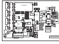
Description Standby power board
The standby power board repeats operation which turns on and off at pin 7 of IC2, and the pulse appears in secondary sides through
the converter transformer T1. At the time, the voltage of 5V at the secondary side is detected by IC3, the negative feedback to IC2 is
carried out at photo coupler ISO1, and the voltage is stabilized. Other outputs are determined by the turn ratio of secondary side of
T1, and the voltage rectified, smoothed through the series regulator (3.3V is stabilized at IC1). On the one hand the voltage rectified
and smoothed by D4 and C16 at primary winding of T1 is supplied as a power supply voltage of IC2 on primary side, and on the
other the voltage of 18V rectified and smoothed By D7 and C28 at primary winding of T1 and stabilized to 15V at IC20 is supplied
as a power supply voltage of IC321 on primary side.
The operation of IC2 is similar to that of IC7 described previously.
Over-Voltage Protection (OVP)
The output voltages of -5V, 3.3V, 5V and 15V are sensed by the pin 13, pin 12, pin 9, pin 10 of IC500 on DNA control board. When
these output voltages are more than 124% of their standard value, the over-voltage protection is created. For example, on the format
DC-DC converter the pin 1 of IC500 will be high and the pin 3 of IC500 will be low then the photo coupler ISO4 will turn off. So the
pin 3 of IC7 is open and IC7 stops to oscillate. The process of over-voltage protection on standby and OEM DC-DC converter is the
same with the OVP on format DC-DC converter. When the voltage of 2.5V exceeds 3.6V the four series diode D81, D82, D83 and
D84 will turn on, then the pin 12 of IC500 will sense the OVP, and IC7 stops to oscillate. When the voltage of 24V exceeds 42V the
zener diode D85 turns on, then the high voltage make the voltage of 3.3V create the over-voltage protection.
Short Circuit Protection
On -5V, 3.3V, 5V and 15V lines, the short circuit protection is carried out by detecting the voltage drop at pin 13, pin 12, pin 9 and pin
10 of IC500, then the under-voltage protection (UVP) is created when the output voltages are less than 80% of their standard value.
For example, on the OEM power board the pin 1 of IC500 will be high and the pin 3 of IC500 will be low, the photo coupler ISO6 will
turn off. The the pin 3 of IC12 is open and IC12 stops to oscillate. The process of under-voltage protection on standby and format
power boardis the same with the UVP on OEM power board. So that the process of short circuit protection is in the same way as
the over-voltage protection described previously, and the short circuit protection is carried out.
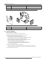
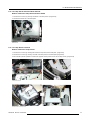
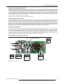
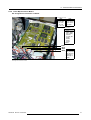
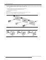
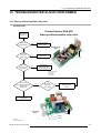
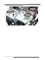
Pin assignment Connectors on Board
J19
D72 (Power Good)
J19
1 PG
2 NC
3 GND
J18
J15
J16
J18
1 ++5V
2 GND
J15
1 ++5V (9A)
2 GND
J16
1 ++24V (1A)
2/4/6 GND
3 ++3.3V (1A)
5 ++5V (1A)
J12
1 375V
2 NC
3 GND P*
* Primary ground
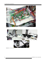
Image 9-9
Pin assignment connectors on board
R5976766 RLM G5 22/04/2004
53