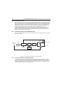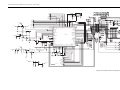
1
EP350 Portable Radios Detailed Service Manual Technical Information Updates As we continue to make engineering enhancements to our products, the information in our Service Manuals need to be updated accordingly. If you wish to be informed of these updates, kindly fill in and fax us your details. Fax to: 6-04-6124944 The Technical Publications Coordinator, Global Customer Documentation, R&D Department, Motorola Penang. Your Details Name/Contact Person: Company Name: Address: Telephone No.: Fax No.: Email Address: How would you like to receive the update notification? Through: mail email fax Manual No.: 6878422A01 Kindly complete the Service Manual Feedback Form on the next page to help us ensure that you receive the most accurate and complete information. Service Manual Feedback Form We believe that reports from users provide valuable information for producing quality manuals. Kindly take a few moments to provide feedback on this manual. Thank you for your cooperation. Fax to: 6-04-6124944 The Technical Publications Coordinator, Global Customer Documentation, R&D Department, Motorola Penang. Not Covered in this Manual Size Too Small Size Adequate Confusing Clear Incorrect Correct Incomplete Complete 1. Please check all the appropriate boxes: Disassembly Procedures Alignment Procedures Exploded Views Schematic Diagrams Circuit Board Details Electrical Parts List Exploded View Parts List 2. How do you rate this particular Service Manual? excellent very good good fair poor 3. Did this Service manual provide you with the information necessary to service and maintain the specific equipment? very much so generally yes to some extent no 4. We would appreciate any corrections or recommendations for improving this manual. Please include the specific page number(s) of the diagram or procedure in question. 5. General comments/suggestions: Manual No.: 6878422A01 i COPYRIGHT Copyrights © 2009 by Motorola, Inc. All rights reserved. No part of this manual may be reproduced, transmitted, stored in a retrieval system, or translated into any language or computer language, in any form or by any means, without the prior written permission of Motorola Inc. Computer Software Copyrights The Motorola products described in this manual may include copyrighted Motorola computer programs stored in semiconductor memories or other media. Laws in the United States and other countries preserve for Motorola certain exclusive rights for copyrighted computer programs including, but not limited to, the exclusive right to copy or reproduce in any form the copyrighted computer program. Accordingly, any copyrighted Motorola computer programs contained in the Motorola products described in this manual may not be copied, reproduced, modified, reverse-engineered, or distributed in any manner without the express written permission of Motorola. Furthermore, the purchase of Motorola products shall not be deemed to grant either directly or by implication, estoppel, or otherwise, any license under the copyrights, patents or patent applications of Motorola, except for the normal non-exclusive royalty-free license to use that arises by operation of law in the sale of a product. Trademarks MOTOROLA and the Stylized M Logo are registered in the U.S.Patent and Trademark Office. All other product or service names are the property of their respective owners. ii SAFETY INFORMATION Product Safety and RF Energy Exposure Compliance These servicing instructions are for use by qualified personnel only. To reduce the risk of electric shock, do not perform any servicing other than that contained in the Operating Instructions unless you are qualified to do so. Refer all servicing to qualified service personnel. Before using this product, read the operating instructions for safe usage contained in the Product Safety and RF Exposure booklet enclosed with your radio. ATTENTION! This is restricted to occupational use only to satisfy ICNIRP RF energy exposure requirements. Before using this product, read the RF energy awareness information and operating instructions in the Product Safety and RF Exposure booklet enclosed with your (Motorola Publication part number 68007024010) to ensure compliance with RF energy exposure limits. For a list of Motorola-approved antennas, and other accessories, visit the following web site which lists approved accessories: http://www.motorola.com/radiosolutions iii DOCUMENT HISTORY The following major changes have been implemented in this manual since the previous edition: Edition Description Date 6878422A01-A Initial edition Mar, 2009 6878422A01-B Added VHF and UHF1 band information (Chapter 8, 9, 10, 11, 12, 13) August, 2009 iv Notes Table of Contents v Table of Contents Copyright ........................................................................................................ i Safety Information......................................................................................... ii Document History ........................................................................................ iii Chapter 1 1.1 1.2 1.3 1.4 1.5 Preventive Maintenance ................................................................................................................ 1-1 Inspection ...................................................................................................................................... 1-1 Cleaning......................................................................................................................................... 1-1 Safe Handling of CMOS and LDMOS............................................................................................ 1-2 General Repair Procedures and Techniques ................................................................................ 1-2 Chapter 2 2.1 2.2 4.2 4.3 DC Power Distribution ........................................................ 3-1 DC Regulation and Distribution ..................................................................................................... 3-1 Chapter 4 4.1 Test Equipment, Service Aids, and Service Tools........... 2-1 Test Equipment.............................................................................................................................. 2-1 Service Aids................................................................................................................................... 2-2 Chapter 3 3.1 Maintenance ........................................................................ 1-1 Controller Theory of Operation.......................................... 4-1 RX Audio Circuit ............................................................................................................................ 4-1 4.1.1 Audio processor IC (U102) ............................................................................................... 4-1 4.1.1.1 RX Audio Processing......................................................................................... 4-1 4.1.1.2 RX Tone PL/Digital PL Decode Filtering............................................................ 4-2 4.1.2 Audio Amp ........................................................................................................................ 4-2 4.1.3 Internal and External Speaker .......................................................................................... 4-2 TX Audio Circuit............................................................................................................................. 4-3 4.2.1 MIC and External MIC ...................................................................................................... 4-3 4.2.2 4-order 4 kHz Low-Pass Filter (U501-C, D) ...................................................................... 4-3 4.2.3 Audio processor IC (U102) ............................................................................................... 4-3 4.2.3.1 TX Audio Processing ......................................................................................... 4-3 4.2.3.2 Tx Tone PL/Digital PL Encode Filtering............................................................. 4-4 4.2.4 TX audio amplifier and 6 order 3 kHz Low-Pass filter....................................................... 4-4 4.2.5 TX modulation Adjustment................................................................................................ 4-4 Microprocessor Circuitry ................................................................................................................ 4-4 4.3.1 Memory Usage ................................................................................................................. 4-5 4.3.2 Control and Indicator Interface ......................................................................................... 4-5 4.3.3 Interface to USB programming ......................................................................................... 4-5 4.3.4 Storage of Customer-Specific Information ........................................................................ 4-5 4.3.5 Sensing of VOX operating ................................................................................................ 4-5 4.3.6 Microprocessor Power-on reset Routine .......................................................................... 4-5 4.3.7 Microprocessor 7.3728 MHz Clock ................................................................................... 4-5 vi Table of Contents 4.3.8 Battery indicator ................................................................................................................ 4-5 Chapter 5 435 – 480 MHz UHF2 Theory Of Operation ....................... 5-1 5.1 5.2 5.3 5.4 5.5 Introduction .................................................................................................................................... 5-1 UHF2 Receiver .............................................................................................................................. 5-1 5.2.1 Receiver Front End ........................................................................................................... 5-2 5.2.2 Receiver Back End ........................................................................................................... 5-2 UHF2 Transmitter .......................................................................................................................... 5-3 5.3.1 Power Amplifier................................................................................................................. 5-3 5.3.2 Antenna Switch ................................................................................................................. 5-3 5.3.3 Harmonic Filter.................................................................................................................. 5-3 5.3.4 Auto Power Control........................................................................................................... 5-4 UHF2 Frequency Generation Circuitry........................................................................................... 5-4 5.4.1 Reference Oscillator (12.8 MHz VCTCXO)....................................................................... 5-4 5.4.2 PLL IC Prescaler and Comparator.................................................................................... 5-5 5.4.3 Voltage Doubler and Charge Pump .................................................................................. 5-5 5.4.4 Loop Filter ......................................................................................................................... 5-5 5.4.5 Dual VCO .......................................................................................................................... 5-5 Keypad........................................................................................................................................... 5-6 Chapter 6 6.1 6.2 6.3 6.4 Troubleshooting Table for Receiver (UHF2) ................................................................................. 6-1 Troubleshooting Table for Synthesizer (UHF2) ............................................................................ 6-2 Troubleshooting Table for Transmitter (UHF2) ............................................................................. 6-3 Troubleshooting Table for Board and IC Signals (UHF2) ............................................................. 6-4 Chapter 7 7.1 7.2 7.3 8.3 8.4 UHF2 Schematic Diagrams, Overlays, and Parts Lists ... 7-1 Introduction .................................................................................................................................... 7-1 7.1.1 Notes For All Schematics and Circuit Boards ................................................................... 7-1 7.1.2 Four Layer Circuit Board ................................................................................................... 7-3 Speaker and Microphone Schematic ............................................................................................. 7-3 7.2.1 Speaker and Microphone Parts List.................................................................................. 7-3 Circuit Board/Schematic Diagram and Parts List (UHF2: 435–480 MHz)...................................... 7-4 7.3.1 Parts List ......................................................................................................................... 7-16 Chapter 8 8.1 8.2 UHF2 Troubleshooting Tables ........................................... 6-1 136 – 174 MHz VHF Theory Of Operation.......................... 8-1 Introduction .................................................................................................................................... 8-1 VHF Receiver................................................................................................................................. 8-1 8.2.1 Receiver Front End ........................................................................................................... 8-2 8.2.2 Receiver Back End ........................................................................................................... 8-2 VHF Transmitter............................................................................................................................. 8-3 8.3.1 Power Amplifier................................................................................................................. 8-3 8.3.2 Antenna Switch ................................................................................................................. 8-3 8.3.3 Harmonic Filter.................................................................................................................. 8-3 8.3.4 Auto Power Control........................................................................................................... 8-4 VHF Frequency Generation Circuitry............................................................................................. 8-4 8.4.1 Reference Oscillator (12.8 MHz VCTCXO)....................................................................... 8-4 8.4.2 PLL IC Prescaler and Comparator.................................................................................... 8-5 Table of Contents 8.5 8.4.3 Voltage Doubler and Charge Pump .................................................................................. 8-5 8.4.4 Loop Filter ......................................................................................................................... 8-5 8.4.5 Dual VCO.......................................................................................................................... 8-5 Keypad........................................................................................................................................... 8-6 Chapter 9 9.1 9.2 9.3 9.4 vii VHF Troubleshooting Tables ............................................. 9-1 Troubleshooting Table for Receiver (VHF) ................................................................................... 9-1 Troubleshooting Table for Synthesizer (VHF) .............................................................................. 9-2 Troubleshooting Table for Transmitter (VHF) ............................................................................... 9-3 Troubleshooting Table for Board and IC Signals (VHF) ............................................................... 9-4 Chapter 10 VHF Schematic Diagrams, Overlays, and Parts Lists.... 10-1 10.1 Introduction .................................................................................................................................. 10-1 10.1.1 Notes For All Schematics and Circuit Boards ................................................................. 10-1 10.1.2 Four Layer Circuit Board................................................................................................. 10-3 10.2 Speaker and Microphone Schematic........................................................................................... 10-3 10.2.1 Speaker and Microphone Parts List................................................................................ 10-3 10.3 Circuit Board/Schematic Diagram and Parts List (VHF: 136–174 MHz)...................................... 10-1 10.3.1 Parts List....................................................................................................................... 10-14 Chapter 11 403 – 447 MHz UHF1 Theory Of Operation ..................... 11-1 11.1 Introduction .................................................................................................................................. 11-1 11.2 UHF1 Receiver ............................................................................................................................ 11-1 11.2.1 Receiver Front End ......................................................................................................... 11-2 11.2.2 Receiver Back End ......................................................................................................... 11-2 11.3 UHF1 Transmitter ........................................................................................................................ 11-3 11.3.1 Power Amplifier............................................................................................................... 11-3 11.3.2 Antenna Switch ............................................................................................................... 11-3 11.3.3 Harmonic Filter ............................................................................................................... 11-3 11.3.4 Auto Power Control......................................................................................................... 11-4 11.4 UHF1 Frequency Generation Circuitry ........................................................................................ 11-4 11.4.1 Reference Oscillator (12.8 MHz VCTCXO) .................................................................... 11-4 11.4.2 PLL IC Prescaler and Comparator.................................................................................. 11-5 11.4.3 Voltage Doubler and Charge Pump ................................................................................ 11-5 11.4.4 Loop Filter ....................................................................................................................... 11-5 11.4.5 Dual VCO........................................................................................................................ 11-5 11.5 Keypad......................................................................................................................................... 11-6 Chapter 12 12.1 12.2 12.3 12.4 UHF1 Troubleshooting Tables ......................................... 12-1 Troubleshooting Table for Receiver (UHF1) ............................................................................... 12-1 Troubleshooting Table for Synthesizer (UHF1) .......................................................................... 12-2 Troubleshooting Table for Transmitter (UHF1) ........................................................................... 12-3 Troubleshooting Table for Board and IC Signals (UHF1) ........................................................... 12-4 Chapter 13 UHF1 Schematic Diagrams, Overlays, and Parts Lists . 13-1 13.1 Introduction .................................................................................................................................. 13-1 viii Table of Contents 13.1.1 Notes For All Schematics and Circuit Boards ................................................................. 13-1 13.1.2 Four Layer Circuit Board ................................................................................................. 13-3 13.2 Speaker and Microphone Schematic ........................................................................................... 13-3 13.2.1 Speaker and Microphone Parts List................................................................................ 13-3 13.3 Circuit Board/Schematic Diagram and Parts List (UHF1: 403–447 MHz).................................... 13-1 13.3.1 Parts List ....................................................................................................................... 13-13 Appendix A Warranty, Service Support, and Replacement Parts .......A-1 A.1 A.2 Scope of Manual ............................................................................................................................A-1 Warranty ........................................................................................................................................A-1 A.2.1 Warranty Period and Return Instructions..........................................................................A-1 A.2.2 After Warranty Period .......................................................................................................A-1 A.2.3 Piece Parts........................................................................................................................A-2 List of Figures ix List of Figures Figure 2-1. Figure 2-2. Figure 2-3. Figure 3-1. Figure 4-1. Figure 4-2. Figure 5-1. Figure 5-2. Figure 5-3. Figure 5-4. Figure 7-1. Figure 7-2. Figure 7-3. Figure 7-4. Figure 7-5. Figure 7-6. Figure 7-7. Figure 7-8. Figure 7-9. Figure 7-10. Figure 7-11. Figure 7-12. Figure 7-13. Figure 7-14. Figure 8-1. Figure 8-2. Figure 8-3. Figure 8-4. Figure 10-1. Figure 10-2. Figure 10-3. Figure 10-4. Figure 10-5. Figure 10-6. Figure 10-7. Figure 10-8. Figure 10-9. Figure 10-10. Figure 10-11. Figure 10-12. Figure 10-13. Figure 10-14. Figure 10-15. Figure 11-1. Figure 11-2. Figure 11-3. Figure 11-4. Figure 13-1. Figure 13-2. Figure 13-3. Programming/Test Cable (PMDN4077_R)....................................................................... 2-3 Cloning Cable (PMDN4076_R) ........................................................................................ 2-3 Wiring of the Connectors.................................................................................................. 2-3 DC Power Distribution Block Diagram.............................................................................. 3-1 RX Audio Circuit ............................................................................................................... 4-1 TX Audio Circuit ............................................................................................................... 4-3 UHF2 Receiver Block Diagram ........................................................................................ 5-1 UHF2 Transmitter Block Diagram .................................................................................... 5-3 UHF2 Frequency Generation Unit Block Diagram ........................................................... 5-4 Keypad Block Diagram..................................................................................................... 5-6 Four–Layer Circuit Board: Copper Steps in Layer Sequence .......................................... 7-3 Speaker and Microphone Schematic ............................................................................... 7-3 UHF2 (435–480 MHz) Receiver Schematic Diagram....................................................... 7-4 VCO and PLL Schematic Diagram................................................................................... 7-5 Transmitter Schematic Diagram....................................................................................... 7-6 Microprocessor and Keypad Schematic Diagram ............................................................ 7-7 Audio Power Amplifier and External Audio Schematic Diagram ...................................... 7-8 Switches and Battery Schematic Diagram ....................................................................... 7-9 Transmitter Audio Filter and Sub-tone Schematic Diagram ........................................... 7-10 UHF2 (435–480 MHz) Mainboard Top Side: PCB No. 8431BEACON200..................... 7-11 UHF2 (435–480 MHz) Mainboard Bottom Side: PCB No. 8431BEACON200 ............... 7-12 UHF2 (435–480 MHz) Sub Circuit Board Top View: PCB No. 8421BEACON100......... 7-13 UHF2 (435–480 MHz) Sub Circuit Board Bottom View: PCB No. 8421BEACON100.... 7-14 UHF2 (435–480 MHz) Keypad Board: PCB No. 8422BEACON100 .............................. 7-15 VHF Receiver Block Diagram........................................................................................... 8-1 VHF Transmitter Block Diagram....................................................................................... 8-3 VHF Frequency Generation Unit Block Diagram.............................................................. 8-4 Keypad Block Diagram..................................................................................................... 8-6 Four–Layer Circuit Board: Copper Steps in Layer Sequence ........................................ 10-3 Speaker and Microphone Schematic ............................................................................. 10-3 VHF (136–174 MHz) Receiver Schematic Diagram....................................................... 10-1 VCO and PLL Schematic Diagram................................................................................. 10-2 Transmitter Schematic Diagram..................................................................................... 10-3 Microprocessor and Keypad Schematic Diagram .......................................................... 10-4 Audio Power Amplifier and External Audio Schematic Diagram .................................... 10-5 Switches and Battery Schematic Diagram ..................................................................... 10-6 Transmitter Audio Filter and Sub-tone Schematic Diagram ........................................... 10-7 Receiver Audio Filter and Sub-tone Schematic Diagram ............................................... 10-8 VHF (136–174 MHz) Mainboard Top Side: PCB No. 8431BEACON400....................... 10-9 VHF (136–174 MHz) Mainboard Bottom Side: PCB No. 8431BEACON400................ 10-10 VHF (136–174 MHz)Sub Circuit Board Top View: PCB No. 8421BEACON100 .......... 10-11 VHF (136–174 MHz)Sub Circuit Board Bottom View: PCB No. 8421BEACON100..... 10-12 VHF (136–174 MHz) Keypad Board: PCB No. 8422BEACON100 .............................. 10-13 UHF1 Receiver Block Diagram ...................................................................................... 11-1 UHF1 Transmitter Block Diagram .................................................................................. 11-3 UHF1 Frequency Generation Unit Block Diagram ......................................................... 11-4 Keypad Block Diagram................................................................................................... 11-6 Four–Layer Circuit Board: Copper Steps in Layer Sequence ........................................ 13-3 Speaker and Microphone Schematic ............................................................................. 13-3 UHF1 (403–447 MHz) Receiver Schematic Diagram..................................................... 13-1 x List of Figures Figure 13-4. Figure 13-5. Figure 13-6. Figure 13-7. Figure 13-8. Figure 13-9. Figure 13-10. Figure 13-11. Figure 13-12. Figure 13-13. Figure 13-14. VCO and PLL Schematic Diagram ................................................................................. 13-2 Transmitter Schematic Diagram ..................................................................................... 13-3 Microprocessor and Keypad Schematic Diagram .......................................................... 13-4 Audio Power Amplifier and External Audio Schematic Diagram .................................... 13-5 Switches and Battery Schematic Diagram ..................................................................... 13-6 Transmitter Audio Filter and Sub-tone Schematic Diagram ........................................... 13-7 UHF1 (403–447 MHz) Mainboard Top Side: PCB No. 8431BEAUHF300 ..................... 13-8 UHF1 (403–447 MHz) Mainboard Bottom Side: PCB No. 8431BEAUHF300 ................ 13-9 UHF1 (403–447 MHz) Sub Circuit Board Top View: PCB No. 8421BEACON100 ....... 13-10 UHF1 (403–447 MHz) Sub Circuit Board Bottom View: PCB No. 8421BEACON100.. 13-11 UHF1 (403–447 MHz) Keypad Board: PCB No. 8422BEACON100 ............................ 13-12 List of Tables xi List of Tables Table 1-1. Table 1-2. Table 2-1. Table 2-2. Table 3-1. Table 4-1. Table 6-1. Table 6-2. Table 6-3. Table 6-4. Table 9-1. Table 9-2. Table 9-3. Table 9-4. Table 12-1. Table 12-2. Table 12-3. Table 12-4. Lead Free Solder Wire Part Number List ......................................................................... 1-3 Lead Free Solder Paste Part Number List ....................................................................... 1-3 Recommended Test Equipment....................................................................................... 2-1 Service Aids ..................................................................................................................... 2-2 Voltage Regulators........................................................................................................... 3-2 Radio Memory Requirements........................................................................................... 4-4 Troubleshooting Table for Receiver (UHF2) .................................................................... 6-1 Troubleshooting Table for Synthesizer (UHF2)................................................................ 6-2 Troubleshooting Table for Transmitter (UHF2) ................................................................ 6-3 Troubleshooting Table for Board and IC Signals (UHF2)................................................. 6-4 Troubleshooting Table for Receiver (VHF)....................................................................... 9-1 Troubleshooting Table for Synthesizer (VHF) .................................................................. 9-2 Troubleshooting Table for Transmitter (VHF)................................................................... 9-3 Troubleshooting Table for Board and IC Signals (VHF)................................................... 9-4 Troubleshooting Table for Receiver (UHF1) .................................................................. 12-1 Troubleshooting Table for Synthesizer (UHF1).............................................................. 12-2 Troubleshooting Table for Transmitter (UHF1) .............................................................. 12-3 Troubleshooting Table for Board and IC Signals (UHF1)............................................... 12-4 xii Notations Used in This Manual Notations Used in This Manual Throughout the text in this publication, you will notice the use of the following notations. These notations are used to emphasize that safety hazards exist, and due care must be taken and observed. Note An operational procedure, practice, or condition that isessential to emphasize. CAUTION indicates a potentially hazardous situation which, if not avoided, might result in equipment damage. Summary of Printed Circuit Boards and Bands Available xiii Summary of Printed Circuit Boards and Bands Available Table below lists all the bands available in this manual. Frequency Band Bandwidth Power Level PC Board Part Number Board Revision Chapter UHF2 435 – 480 MHz 1W or 4W 8431BEACON200 2 7 UHF2 – – 8421BEACON100 1 7 UHF2 – – 8422BEACON100 1 7 VHF 136 – 162 MHz 1W or 5W 8431BEACON400 4 10 VHF – – 8421BEACON100 1 10 VHF – – 8422BEACON100 1 10 UHF1 403 – 447 MHz 1W or 4W 8431BEAUHF300 3 13 UHF1 – – 8421BEACON100 1 13 UHF1 – – 8422BEACON100 1 13 xiv Notes Chapter 1 Maintenance 1.0 Introduction This chapter of the manual describes: • Preventive maintenance • Safe handling of CMOS devices • Repair procedures and techniques NOTE 1.1 The Servicing of your Intrinsically Safe Radios. In order to maintain compliance, radios that are FM Approved to intrinsically safe standards MUST be repaired at FM audited service centers. See Further Assistance From Motorola on page 1-2 for more information. Preventive Maintenance Periodic visual inspection and cleaning is recommended. 1.2 Inspection Check that the external surfaces of the radio are clean, and that all external controls and switches are functional. It is not recommended to inspect the interior electronic circuitry. 1.3 Cleaning The following procedures describe the recommended cleaning agents and the methods to be used when cleaning the external and internal surfaces of the radio. External surfaces include the front cover, housing assembly, and battery case. These surfaces should be cleaned whenever a periodic visual inspection reveals the presence of smudges, grease, and/or grime. NOTE Internal surfaces should be cleaned only when the radio is disassembled for servicing or repair. The only recommended agent for cleaning the external radio surfaces is a 0.5% solution of a mild dishwashing detergent in water. The only factory recommended liquid for cleaning the printed circuit boards and their components is isopropyl alcohol (100% by volume). CAUTION: The effects of certain chemicals and their vapors can have harmful results on certain plastics. Aerosol sprays, tuner cleaners, and other chemicals should be avoided. 1. Cleaning External Plastic Surfaces The detergent-water solution should be applied sparingly with a stiff, non-metallic, shortbristled brush to work all loose dirt away from the radio. A soft, absorbent, lintless cloth or tissue should be used to remove the solution and dry the radio. Make sure that no water remains entrapped near the connectors, cracks, or crevices. 1-2 Introduction 2. NOTE 1.4 Cleaning Internal Circuit Boards and Components Isopropyl alcohol may be applied with a stiff, non-metallic, short-bristled brush to dislodge embedded or caked materials located in hard-to-reach areas. The brush stroke should direct the dislodged material out and away from the inside of the radio. Make sure that controls or tunable components are not soaked with alcohol. Do not use high-pressure air to hasten the drying process since this could cause the liquid to collect in unwanted places. Upon completion of the cleaning process, use a soft, absorbent, lintless cloth to dry the area. Do not brush or apply any isopropyl alcohol to the frame, front cover, or back cover. Always use a fresh supply of alcohol and a clean container to prevent contamination by dissolved material (from previous usage). Safe Handling of CMOS and LDMOS Complementary metal-oxide semiconductor (CMOS) devices are used in this family of radios. CMOS characteristics make them susceptible to damage by electrostatic or high voltage charges. Damage can be latent, resulting in failures occurring weeks or months later. Therefore, special precautions must be taken to prevent device damage during disassembly, troubleshooting, and repair. Handling precautions are mandatory for CMOS circuits and are especially important in low humidity conditions. DO NOT attempt to disassemble the radio without first referring to the CMOS CAUTION paragraph in the Disassembly and Reassembly section of the manual. 1.5 General Repair Procedures and Techniques NOTE Environmentally Preferred Products (EPP) (refer to the marking on the printed circuit boards - examples shown below) were developed and assembled using environmentally preferred components and solder assembly techniques that meet or exceed compliance to the European Union’s ROHS and WEEE directives (Waste Electrical and Electronic Equipment (WEEE) Directive 2002/96/EC and Restriction of Hazardous Subtances (ROHS) Directive 2002/95/EC). To maintain product compliance and reliability, use only the Motorola specified parts in this manual. For the identification of lead (Pb) free assemblies, all EPP products will carry the EPP Marking, shown below, on the printed circuit board (PCB). This marking provides information to those performing assembly, servicing and recycling operation on this product, adhering to the JEDEC standard #97. The EPP Marking takes the form of a label or marking on the PCB. Introduction 1-3 Any rework or repair on Environmentally Preferred Products must be done using the appropriate lead-free solder wire and solder paste as stated in the following tables: Table 1-1. Lead Free Solder Wire Part Number List Motorola Part Number Alloy Flux Type Flux Content by Weight Melting Point Supplier Part number Diamet er Weight 1088929Y01 95.5Sn/3.8Ag/0.7Cu RMA Version 2.7-3.2% 217C 52171 0.015” 1lb spool Table 1-2. Lead Free Solder Paste Part Number List Motorola Part Number Manufacturer Part Number 1085674C03 NC-SMQ230 Viscosity Type Composition & Percent Metal 900-1000KCPs Brookfield (5rpm) Type 3 (-325/+500) (95.5%Sn-3.8%Ag-0.7%Cu) 89.3% Liquid Temperatur e 217°C Parts Replacement and Substitution When damaged parts are replaced, identical parts should be used. If the identical replacement component is not locally available, check the parts list for the proper Motorola part number and order the component from the nearest Motorola Communications parts center listed in the “Piece Parts” section of this manual. Rigid Circuit Boards The family of radios uses bonded, multi-layer, printed circuit boards. Since the inner layers are not accessible, some special considerations are required when soldering and unsoldering components. The through-plated holes may interconnect multiple layers of the printed circuit. Therefore, care should be exercised to avoid pulling the plated circuit out of the hole. When soldering near the connector pins: • Avoid accidentally getting solder in the connector. • Be careful not to form solder bridges between the connector pins • Closely examine your work for shorts due to solder bridges. Chip Components Use the RLN4062 Hot-Air Repair Station for chip component replacement. Adjust the temperature control to 390 °C (735 °F), and adjust the airflow to a minimum setting. Airflow can vary due to component density. • To remove a chip component: 1. Use a hot-air hand piece and position the nozzle of the hand piece approximately 0.3 cm (1/8") above the component to be removed. 2. Begin applying the hot air. Once the solder reflows, remove the component using a pair of tweezers. 3. Using a solder wick and a soldering iron or a power desoldering station, remove the excess solder from the pads. 1-4 Introduction • • To replace a chip component using a soldering iron: 1. Select the appropriate micro-tipped soldering iron and apply fresh solder to one of the solder pads. 2. Using a pair of tweezers, position the new chip component in place while heating the fresh solder. 3. Once solder wicks onto the new component, remove the heat from the solder. 4. Heat the remaining pad with the soldering iron and apply solder until it wicks to the component. If necessary, touch up the first side. All solder joints should be smooth and shiny. To replace a chip component using hot air: 1. Use the hot-air hand piece and reflow the solder on the solder pads to smooth it. 2. Apply a drop of solder paste flux to each pad. 3. Using a pair of tweezers, position the new component in place. 4. Position the hot-air hand piece approximately 0.3 cm (1/8”) above the component and begin applying heat. 5. Once the solder wicks to the component, remove the heat and inspect the repair. All joints should be smooth and shiny. Shields Removing and replacing shields is recommended to be done with the Air Blower, BOSCH GHG 603 or equivalent. • • To remove the shield: 1. Place the circuit board in the circuit board holder. 2. Add solder paste flux around the base of the shield. 3. Position the heat-focus head onto the shield. 4. Turn on the heater and wait until the shield lifts off the circuit board. 5. Once the shield is off, turn off the heat, and grab the part with a pair of tweezers. 6. Remove the circuit board from the circuit board holder. To replace the shield: 1. Add solder to the shield if necessary, using a micro-tipped soldering iron. 2. Next, rub the soldering iron tip along the edge of the shield to smooth out any excess solder. Use solder wick and a soldering iron to remove excess solder from the solder pads on the circuit board. 3. Place the circuit board back in the circuit board holder. 4. Place the shield on the circuit board using a pair of tweezers. 5. Position the heat-focus head over the shield. 6. Turn on the heater and wait for the solder to reflow. 7. Once complete, turn off the heat, raise the heat-focus head and wait approximately one minute for the part to cool. 8. Remove the circuit board and inspect the repair. No cleaning should be necessary. Chapter 2 Test Equipment, Service Aids, and Service Tools 2.1 Test Equipment Table 2-1 lists test equipment required to service the radios. Table 2-1. Recommended Test Equipment Motorola Part No. Description Characteristics Application R2600 series or HP 8920A System analyzer This item will substitute for items with an asterisk (*) Frequency/Deviation meter and signal generator for wide-range troubleshooting and alignment *R1074A Fluke 87 digital multi-meter True RMS metering, 200 kHz frequency counter, 32-segment bar graph with backlit display Digital voltmeter is recommended for AC/DC voltage and current measurements Fluke 85 RF probe 500 MHz, 30 VAC max Use with Fluke 87 digital multi-meter for RF voltage measurements. *R1377A AC voltmeter 1 mV to 300 mV, 10 mega- Audio voltage measurements Ohm input impedance R1611A Dual channel 100 MHz oscilloscope (Agillent) Two-channel, 100 MHz bandwidth, 200 M sample rate/sec, 2 MB memory/ channel Waveform measurements S1339A RF millivolt meter 100 μV to 3V RF, 10 kHz to 1 GHz frequency range RF level measurements *R1013B or SINAD meter or Receiver sensitivity measurements *R1370A SINAD meter with RMS Without RMS audio voltmeter or With RMS audio voltmeter 2-2 2.2 Test Equipment, Service Aids, and Service Tools: Service Aids Service Aids Table 2-2 lists the service aids recommended for working on the EP350 Series Radios. While all of these items are available from Motorola, most are standard shop equipment items, and any equivalent item capable of the same performance may be substituted for the item listed. Table 2-2. Service Aids Motorola Part No. Description Application PMDN4026_R Flat Ceramic Tuning Tools (1.8mm) Used for tuning the VCO. PMDN4038_R Knob Remover/Chassis Opener Used to remove the front cover assembly. PMDN4039_R Crab Eye Nut Opener Used to remove the crab eye nut. PMDN4040_R1 Radio Test Box Enables communication between the radio, test equipment and the computer's USB port. PMDN4041_R RF Adapter Adapts radio’s antenna port to BNC cabling of test equipment. PMDN4044_R T-Head Ceramic Tuning Tool Used for tuning the VCO. PMDN4053_R Flat Ceramic Tuning Tools (0.9mm) Used for tuning the VCO. PMDN4076_R Radio to Radio Cloning Cable Allows a radio to be duplicated from a master radio by transferring programmed data from the master radio to the other. PMDN4077_R Programming Cable Used to program the radio through Customer Programming Software and Radio Tuner. PMDN4079_R GND Plate Interconnects radio’s chassis to RF Adaptor. PMDN4080_R Battery Eliminator Interconnects radio to power supply. PMVN4161_ Customer Programming Software on CD Rom Program customer option and channel data. PMVN4165_ Tuner on CD Rom Only Motorola Service Centers or Authorized Motorola Service Dealers can perform this function. Note: 1.Use PMDN4040BR or higher for tuning the EP350 Series radios as PMDN4040AR cannot be used to perform this function. Test Equipment, Service Aids, and Service Tools: Service Aids 2-3 Programming/Test Cable 2.5mm stereo USB connection t Figure 2-1. Programming/Test Cable (PMDN4077_R) 2.5mm stereo ~ 2.5mm stereo Figure 2-2. Cloning Cable (PMDN4076_R) D+ D- VBUS TX_D 1 RX_D 2.5mm stereo > 2 2 3 VBUS DD+ To Computor GND 4, 5, 6 GND IC : CP2102 1 RX / TX data 1 2 GND Figure 2-3. Wiring of the Connectors USB_CONNECTOR 2-4 Test Equipment, Service Aids, and Service Tools: Service Aids Notes Chapter 3 DC Power Distribution 3.1 DC Regulation and Distribution A block diagram of the DC power distribution throughout the radio is shown in Figure 3-1. VCTCXO Vdd Regulator 5V Audio filter ½ Vcc Voltage Doubler VCO 10V Charge Pump SWB+ 7.5V Battery RX B+ TXVB Mech SW1 PA Vdd Regulator APC Key PCB 3.3V MCU, EEPROM PLL IC Digital potentiometer Driver, Pre-driver Low Batt. detector DTMF IC LCD Driver Audio Amplifier Figure 3-1. DC Power Distribution Block Diagram Battery voltage enters at connector J602 and is routed through SW/VOL1 to become SWB+. This voltage is routed to: • SW/VOL1 • TX power amplifier Q403 (via R417) • APC circuit U401 • RX audio power amplifier U601 • 5V regulator (U505) • 3.3V regulator (U506) • Voltage divider R153/R154, a microprocessor A/D input which measures battery voltage • Key PCB 3-2 DC Power Distribution: DC Regulation and Distribution The following regulators are used: Table 3-1. Voltage Regulators Reference No. Description Type U505 5V regulator TK11250 U506 3.3V regulator TK11233 U507 Voltage Doubler (10V) TC12140 The 5 V source from U505 is applied to: • RX back end circuitry • RX/TX audio filters • 1/2 VCC generator • VCO power source (Q705, Q706) • RX B+ (Q304) • TXVB (Q407) • VCTCXO The 5 V source is also applied to transistor switches Q304 and Q407. Q304 is turned on by Q305 when RX_EN (from U101 Pin 71) is high, and supplies the source to mixer, IF IC and LNA. Q407 is turned on by Q408 when TX_EN2 (from U101 Pin 85) is high, and supplies the "TXVB" source to the first transmitter stage Q401 base, Q402 gate, APC power source (U401 Pin 8) and ANT switch (CR401). The 3.3 V regulated source from U506 is applied to: • MCU IC U101 • EEProm IC U104 • DTMF IC U103 • Audio processor IC U102 • Microphone bias circuitry • And applied to Key PCB (LCD driver power source) The 10 V source from U507 is applied to Charge Pump. Chapter 4 Controller Theory of Operation 4.1 RX Audio Circuit The RX audio circuit consists of Audio Processor IC, Audio Amplifier, Internal (INT)/External (EXT) speaker and Sub-Audio Tones System. Audio Processor IC (AK2347) RXA1 Audio IN (from IF IC) RX LPF TX/RX HPF Scrambler/ Descrambler VR3 pin24 Deemphasis Expander -4 to +3.5dB/ 0.5dB VR4 SMF -18, -4.5 to +4.5dB/ 0.25dB pin21 U102 Sub audio Programmable LPF -6 to +6dB/ 0.5dB Audio Amp. Vol1 INT SPK. VR5 J601 IN- OUT- IN+ pin18 Sub audio HPF OUT+ U105-A,B U601 SVR EXT SPK. Comparator To CPU (tone detect) U105-C Audio Mute control Figure 4-1. RX Audio Circuit 4.1.1 Audio processor IC (U102) The RX audio from Pin 9 of U201 enters to Pin 24 of Audio processor IC. • RX A: An operational amplifier used for gain adjustment of the receive demodulation signal from Pin 9 of U201. The gain is unity and it acts as a buffer amplifier. 4.1.1.1 RX Audio Processing • VR3: This circuit controls the volume for adjusting the input level of receive demodulation signal. Adjustment range: -4.0dB to +3.5dB in 0.5dB steps. • RX LPF: Low-pass filter to eliminate high-frequency components higher than 3 kHz which are included in the receive demodulation signal. • TX/RX HPF: High-pass filter to eliminate low-frequency components lower than 250 Hz which are included in receive audio signal. This circuit is turned on and off by control register of Audio processor IC. • Descrambler: This circuit inverts the spectrum distribution of receive audio signals with respect to the carrier frequency. The carrier frequency is 3.388 kHz or 3.290 kHz. 4-2 Controller Theory of Operation: RX Audio Circuit • De-emphasis: This circuit restores the original state of signal of which high-frequency component has been emphasized by the pre-emphasis. • Expander: This circuit expands the signal compressed twice by the Compressor in dB scale to restore the original signal state. • VR4: This circuit controls the volume for adjusting the RX output level. Adjustment range: -18.0dB, -4.5dB to +4.5dB in 0.25dB steps. • SMF: Smoothing filter to eliminate the high-frequency and clock components generated in the Audio processor IC. 4.1.1.2 RX Tone PL/Digital PL Decode Filtering • Sub-audio Programmable LPF: Low-pass filter to eliminate components of the RXA1 signal. This circuit is controlled by the internal registers and by the audio processor IC for cut-off frequency. • VR5: This circuit controls the volume for adjusting the output level from the sub-audio LPF signal. Adjustment range: -6.0dB, +6.0dB in 0.5dB steps The sub-audio tone of U102 Pin 18 output pass through switchable high-pass filter U105. This filter (U105-A, B) has 4 different high pass cut-off frequencies which can be selected accordingly to the sub-tone audio. This filter (U105-A, B) filters the unwanted sub-tone. The tone of U105-B output passed through U105-C comparator, which acts as a squaring circuit. This output signal is then sent to microprocessor Pin 3. The micro-processor then decodes CTCSS and CDCSS from this square signal. 4.1.2 Audio Amp The de-emphasized audio signal from Pin 21 of audio processor IC passes through volume control (SW/VOL1) and is amplified by U601BTL audio amplifier to a sufficient level to drive a loud speaker. U601 has mute/un-mute function controlled by audio-mute control (Pin 83) of CPU. When U601 Pin 1 is low, the audio amp goes to active (un-mute) mode. When U601 Pin 1 is high, the audio amp goes to mute mode. 4.1.3 Internal and External Speaker When no external speaker is plugged into J601, the RX audio is passed through to the internal speaker. When an external speaker is plugged into J601, the internal speaker is cut-off from the rest of the circuit and RX audio is passed through the external speaker. Controller Theory of Operation: TX Audio Circuit 4.2 4-3 TX Audio Circuit The TX audio circuit consists of MIC/External MIC, LPF, Audio processor IC, and TX Sub-tone system. For UHF1 and UHF2, refer to Figure 4-2. For VHF, refer to Figure 4-3. 4 Order LPF (Fc=4KHz) Mic (Audio IN) Audio Processor IC (AK2347) U501-C,D TX/RX HPF TXA1 VR1 (HPF) pin4 Compressor Scrambler/ Descrambler PreEmphasis -6 to +4.5dB/ 1.5dB Limiter VR2 Splatter SMF -9.6 to +3dB/ Fc=2.55KHz/ 0.2dB 3KHz Fc=300Hz pin8 U102 DTA1 Tone IN (from CPU) Sub audio Programmable -6 to +6dB/ LPF 0.5dB 2 Order LPF (Fc=300Hz) 6 Order LPF (Fc=3KHz) TX AF Amp. pin19 VR5 Mod.Adj, pin17 U502-C U508 U501-A,B U502-A To VCO & VCTCXO Figure 4-2. TX Audio Circuit (UHF1 and UHF2) 4 Order LPF (Fc=4KHz) Mic (Audio IN) Audio Processor IC (AK2347) U501-C,D TX/RX HPF TXA1 pin4 VR1 (HPF) Compressor Scrambler/ Descrambler PreEmphasis -6 to +4.5dB/ 1.5dB Limiter VR2 Splatter -9.6 to +3dB/ Fc=2.55KHz/ 0.2dB 3KHz Fc=300Hz pin8 U102 DTA1 Tone IN (from CPU) SMF Sub audio Programmable -6 to +6dB/ LPF 0.5dB 2 Order LPF (Fc=300Hz) 6 Order LPF (Fc=3KHz) TX AF Amp. pin19 Mod.Adj, VR5 pin17 U501-A,B U502-A To VCO & VCTCXO Figure 4-3. TX Audio Circuit (VHF) U502-C U508 4-4 4.2.1 Controller Theory of Operation: TX Audio Circuit MIC and External MIC The TX audio enters the radio via the internal MIC or the external MIC jack. When using the internal MIC, the audio passes through the external jack then rest of the circuits. When using the external jack, the audio from the internal MIC is cut-off from the rest of the circuits and the external MIC audio is passed to the rest of the circuits. 4.2.2 4-order 4 kHz Low-Pass Filter (U501-C, D) 4-order 4 kHz Low-pass filter to prevent aliasing noise of the ASIC switching cut-off frequency. 4.2.3 Audio processor IC (U102) 4.2.3.1 TX Audio Processing Tx Audio from Pin 14 of U501-D enters the ASIC at Pin 3, 4 (Internal TX AMP). • TX A1: Operational amplifier for gain adjustment of TX audio signal. R102, R103, C102, C103 are used to set the gain. • VR1 (HPF): This circuit controls the volume for adjusting the input level of TX audio signal. Adjustment range: -6.0dB, +4.5dB in 1.5dB steps • Compressor: This circuit compresses the amplitude of transmit audio signal by 1/2 in dB scale. • Pre-emphasis: This circuit emphasizes the high-pass frequency component of TX audio signal to improve the S/N ratio of the modulation signal. • TX/RX HPF: High-pass filter to eliminate low-frequency components lower than 250 Hz which are included in transmitter audio signal. This circuit is turned on and off by control register of Audio Processor IC. • Scrambler: This circuit inverts the spectrum distribution of transmitter audio signals with respect to the carrier frequency. The carrier frequency is 3.388 kHz or 3.290 kHz. • Limiter: Amplitude limiting circuit to suppress frequency deviation in the modulation signal. The limit level can be adjusted by applying a DC voltage the LIMLV Pin 7. When the pin is left open, the level predetermined within the device is output. • VR2: This circuit controls the volume for adjusting the output level on the MOD Pin 8. Adjustment range: -9.6dB to +3.0dB in 0.2dB steps. • Splatter: Low-pass filter to eliminate high-frequency components higher than 3 kHz which are included in the limiter output signal. The cut-off frequency is 3 kHz. • SMF: Smoothing filter to eliminate the high-frequency and clock components generated in the ASIC. 4.2.3.2 Tx Tone PL/Digital PL Encode Filtering The encode circuit of CTCSS and CDCSS mixes signals from 4 ports of microprocessor. This mixed signal passes through ASIC Pin 19, 20 (U102). • DTA1: Amplifier for gain adjustment of sub-audio signal which generated from CPU. Use external resistor and capacitor to set the gain. • Sub-audio Programmable LPF: Low-pass Filter to eliminate components of DAT1 signal in the transmitter. This circuit is controlled cut-off frequency by the internal ASIC registers. • VR5: This circuit controls the volume for adjusting the output level from the Sub-Audio LPF signal. Adjustment range: -6.0dB to +6.0dB in 0.5 steps. Controller Theory of Operation: Microprocessor Circuitry 4.2.4 4-5 TX audio amplifier and 6 order 3 kHz Low-Pass filter The TX audio signal from ASIC Pin 8 (UHF1, UHF2) or U508 Pin 4 (VHF) is linked by TX audio amp (U502-C) to increase limiting range. The limited audio signal is adjusted to a proper level by U508 and passes through 6 order 3 kHz low pass filter (U501-A,B) before being modulated. 4.2.5 TX modulation Adjustment TX audio signal from Pin 8 of U502-C (UHF1, UHF2) or Pin 8 of ASIC (VHF) is linked TX modulation adjustment IC (U508). The TX modulation is tuned in the factory. If any of the TX part is replaced, the TX modulation must be tuned using Tuner. 4.3 Microprocessor Circuitry The microprocessor circuitry includes microprocessor (U101) and associated EEPROM. Table 4-1. Radio Memory Requirements Reference No. U101 U104 4.3.1 Description Microprocessor Serial EEPROM Size Flash ROM 128 Kbyte * 8 RAM 5 Kbyte * 8 8 Kbit * 8 Memory Usage Radio operation is controlled by software that is stored in internal Flash ROM memory. Radio parameters and customer specific information is stored in External EEPROM (U104). The operating status of the radio is maintained in RAM located within the microprocessor. When the radio is turned off, the operating status of the radio is written to EEPROM before operating voltage is removed from the microprocessor. 4.3.2 Control and Indicator Interface Ports Pin 35 and 36 are outputs which control the Sub-PCB mounted LED indicator. When Pin 35 is high, the indicator is green. When Pin 36 is high, the indicator is red. When both are high, the indicator is amber. When both are low, the indicator id is off. Pressing the side-mounted PTT button (PB501) provides a low to port Pin 44, which indicates PTT is asserted. Side-mounted function buttons 1 & 2 (PB502 and PB503) are connected to port Pin 21 and Pin 32, respectively. 4.3.3 Interface to USB programming The radio can be programmed, or the programmed information can be read, using a computer with CPS (Customer Programming Software) connected to the radio via a USB Programming cable (PMDN4077A). Connection to the radio is made via the microphone connector (part of accessory connector J601). The line connects the programming connect (J601 Pin 6) to port PRG/CLONE_RX (data into uP, Pin 34) and PRG/CLONE_TX(data out of uP, Pin 33). 4.3.4 Storage of Customer-Specific Information Information that has been programmed using CPS, such as channel frequencies or selective signaling codes, etc, are stored in the external EEPROM, where it is retained permanently (unless reprogrammed) without needing DC power applied to the microprocessor. 4-6 4.3.5 Controller Theory of Operation: Microprocessor Circuitry Sensing of VOX operating Port PTT2 (Pin 68) is used to detect the presence of VOX operating when externally connected accessories with VOX enabled. When port PTT2 is low, the VOX will start to operate. 4.3.6 Microprocessor Power-on reset Routine On power-up, the microprocessor is held in reset until the digital 3.3V regulator (U506 Pin 4) provides a stable supply voltage. Once the digital supply reaches steady state and releases the reset line (U107 Pin 2), the microprocessor begins to start up. After reset release by all circuit, the software within the microprocessor begins executing port assignment, RAM checking, and initialization. 4.3.7 Microprocessor 7.3728 MHz Clock The 7.3728 MHz clock signal (Pin 13, X-in) is provided from the FL101. 4.3.8 Battery indicator Various battery types are available having different capacities. The radio can select different battery type by FPP (Front Panel Programming) or CPS. A voltage divided by R153 and R154. And EEPROM have a data for each battery types. Chapter 5 435 – 480 MHz UHF2 Theory Of Operation 5.1 Introduction This chapter provides a detailed theory of operation for the radio components. Schematic diagrams for the circuits described in the following paragraphs are located in Chapter 7 of this manual. 5.2 UHF2 Receiver The UHF2 receiver design covers the frequency range of 435 – 480 MHz and it is a double conversion super heterodyne with 1st IF 45.1 MHz and 2nd IF 455 kHz. The receiver is divided into two major blocks, Front End and Back End as shown in Figure 5-1. Preselector Filter RF Amp Postselector Crystal IF 1st Mixer Filter Amp Filter RX from Antenna Switch Inj Filter First LO from Synthesizer N/S_SW Descriminator 455C24 LPF Recovered Audio Quadrature Detector Ceramic Filter 455FW 455HW IF Amp RSSI Crystal 44.645MHz Figure 5-1. UHF2 Receiver Block Diagram 5-2 5.2.1 435 – 480 MHz UHF2 Theory Of Operation: UHF2 Receiver Receiver Front End Incoming RF signals from antenna are first routed through the harmonic filter (L409, L410, L411, C426, C427, C428, C429, C445, C446) and antenna switch (CR301), part of the transmitter circuitry, before being applied to the receiver front end. The receiver front end consists of preselector filter, RF amplifier, post-selector filter and a single-balanced mixer. The preselector filter is a varactor-tuned 2-pole design using discrete elements (L320, L324, C351, C352, C353, C354, C355, C356, C357, C358, C359, C360, C361) in a series/shunt resonator configuration. It is a band-shift filter and the frequency shift is controlled by varactor diodes CR314 and CR307, which are connected to the microprocessor. It is configured to provide steeper attenuation above the passband for improved spurious rejection when low-side local injection is used. The frequency is separated into 8 steps and controlled by CPU (435 – 480 MHz). The output of this filter is matched to the base of RF amplifier Q301 which provides 13dB of gain. The output of the RF amplifier is applied to the post-selector filter. The post-selector filter designed using discrete elements (L322, L323, L328, C379, C354, C355) in a series/shunt resonator configuration. It is a band-shift filter and the frequency shift is controlled by varactor diodes CR313, CR304 and CR305, which are connected to the microprocessor. It is configured to provide steeper attenuation above the passband for improved spurious rejection when low-side local injection is used. The frequency is separated into 8 steps and controlled by CPU (435 – 480 MHz). The output of the post selector is connected to the single-balanced mixer consisting of components L329, L333, Q306 and Q307. 1st local signal generated from VCO is filtered by injection filter (L310, L331, C325, C326, C327) to remove second harmonics. The converted 1st IF frequency at mixer passes through L331 and matches the 45.1 MHz IF signal to pair crystal filter (FL301). 5.2.2 Receiver Back End The 1st IF signal is amplified about 15 dB by IF amp Q303. The output of the IF amp is connected to IF IC (U201). 1st IF frequency (45.1 MHz) and 2nd LO frequency (44.645 MHz) are mixed in U201. The second mixer converts the 45.1 MHz high IF frequency to 2nd IF frequency (455 kHz). Additional IF selectivity is provided by two ceramic filters (CF1, CF2). The wider filter 455 FW is used for 25 kHz channel spacing, and the narrower filter 455 HW is used for 12.5 kHz channel spacing. These two ceramic filters may eliminate undesired signal and demodulated by demodulator in U201. N/S_SW which connected to microprocessor is used to select the wide and narrow band. The mute (squelch) circuit switches off the audio amplifier when no audio is present. The squelch circuit consists of U201 and U202 and their associated components. The noise signal from Pin 9 of U201 is used to control the squelch circuit sensitivity of U202. The noise passes through filter, and is amplified by internal amp of U201. The amplified noise act as a DC voltage to control the mute system. So if the noise level is under the threshold voltage, the microprocessor (U101) un-mutes the radio. If the noise level is over the threshold voltage, the microprocessor mutes the radio. The squelch level is tuned in the factory. When a component or a part in the RX system is replaced, the squelch must be re-tuned using the Tuner. 435 – 480 MHz UHF2 Theory Of Operation: UHF2 Transmitter 5.3 5-3 UHF2 Transmitter The UHF2 transmitter covers the range of 435 – 480 MHz. Depending on model, the output power of the transmitter is switchable on a per-channel basis between high power (4 Watts) and low power (1 Watt). The transmitter is divided into four major blocks as shown in Figure 5-2. • • • • Power Amplifier Harmonic Filter Antenna Matching Network Power Control. SWB+ BAT+ Power Control Current Detect CR401 From VCO Attenuator Circuit Antenna Strip Line Pre Driver Amp Driver Amp Final Amp Harmonic Filter To Receiver Antenna Switch Figure 5-2. UHF2 Transmitter Block Diagram 5.3.1 Power Amplifier The transmitter power amplifier has three stages of amplification – Pre Driver (Q401), Driver Amp (Q402) and Final Amp (Q403). Signal from TX VCO is applied to the pre driver via an attenuator circuit. The attenuator is pie style resistor attenuator, and is used as isolation between VCO and the power amps. The -4dBm TX RF signal from attenuator is then amplified by pre driver and driver amp to around +25dBm and is applied to the final amp. The final amp (Q403) is an enhancement-mode N-channel MOSFET device providing a gain of 12dB. The device drain current is drawn directly from the DC battery supply voltage input via L413. A matching network consisting of C416 to C420 and a strip line, transforms the impedance to approximately 50 Ohm. 5.3.2 Antenna Switch An antenna switch works mainly as a switching device between transmit and receive paths. In transmit mode (PTT), Q407 is turned on and both PIN diodes (CR401, CR301) are forward biased into conduction. This enables the RF signal to pass to the harmonic filter and then to the antenna. In the receiver mode, both diodes are off. Signals applied to the antenna jack are routed via the LPF (harmonic filter), through network L409 to L411, to the receiver input. 5.3.3 Harmonic Filter The harmonic filter consists of components L409, L410, L411, C426, C427, C428, C429, C430, C445 and C446. The harmonic filter is a seven-pole Chebychev filter. 5-4 5.3.4 435 – 480 MHz UHF2 Theory Of Operation: UHF2 Frequency Generation Circuitry Auto Power Control The APC keeps the current supply constant to the final amp (Q403). The drain current of Q403 (final amp) is sensed across resistor R417. The voltage difference across R417 is amplified through U401 by the ratio of R423 to R417. The differential signal at the output of U401 (Pin 7) is passed to Q404 and Q405 that produces a constant power output to the antenna. If the current is changed due to change of battery voltage or load, APC controls gate voltage of Q403 and collector voltage of Q401 and drain voltage of Q402 to keep TX power stable. This circuit stabilizes TX power at a pre-determined level adjusted by U402. This bias voltage is tuned in the factory. If the transistor (Q403) is replaced, the RF Output Power must be tuned. By tuning the RF output power, the bias voltage will be tuned through U402. Extra care has to be taken during the tuning process. Do not exceed the maximum allowed bias voltage. 5.4 UHF2 Frequency Generation Circuitry The PLL synthesizer subsystem consists of the reference oscillator (VCTCXO), VCO, PLL IC, Charge Pump and Loop Filter. TX VCO Circuit FL701 Modulating Signal TX Out Synthesizer U701 Charge Pump Loop Filter 12.8MHz Ref.OSC. PLL Data from μP To PA Driver Voltage Doubler RX Out RX VCO Circuit To Mixer Figure 5-3. UHF2 Frequency Generation Unit Block Diagram 5.4.1 Reference Oscillator (12.8 MHz VCTCXO) The reference oscillator is powered by regulated 5V provided by U505. The reference frequency 12.8 MHz VCTCXO (Voltage Controlled Temperature Compensated Crystal Oscillator) is applied to the PLL IC (U701) via Pin 1. Main frequency can be adjusted by chip trimmer of VCTCXO. This frequency provides reference to the PLL IC and has a frequency stability of +/-2.5PPM (max) at the temperature ranging from -30 to +60 Degree Celsius. 435 – 480 MHz UHF2 Theory Of Operation: UHF2 Frequency Generation Circuitry 5.4.2 5-5 PLL IC Prescaler and Comparator The reference frequency from VCTCXO is divided to 6.25 kHz or 5 kHz by reference counter, R. The RF signal input from the VCO is divided to by prescaler (1/64), divided by N and A counters in PLL IC to determine frequency steps and then supplied to the comparator. The comparison frequency is 6.25/5 kHz. The internal phase comparator compares the phase difference between the reference and VCO signal. When the phase of the reference frequency is leading, Pin15 (R) is the output. When VCO frequency is leading, Pin 16 (P) is the output. When P=R, small pulses are the output of the phase detector. 5.4.3 Voltage Doubler and Charge Pump The voltage doubler (U507) converts 5V to 10V and is applied to the charge pump circuitry. The charge pump is used for charging output signals P, R supplied by PLL IC from 0-3.3V to 0-10V. This voltage is used to drive the VCO. 5.4.4 Loop Filter The loop filter contains C751, C752, C753, C754, R726, R727, R728. It reduces the residual sideband noise to get the best signal-to-noise ratio. The output signal from loop filter is applied to VCO. 5.4.5 Dual VCO The dual VCO module contains a RX VCO and a TX VCO. They are configured as colpitts oscillators and connected to power up through transistor switches. Only one VCO is selected at a time. A steering line voltage between 0.35V and 9.7V at varactor CR701 tunes the full RX frequency range from 389.9MHz to 434.9MHz, and varactor CR702 tunes the full TX frequency range from 435MHz to 480MHz. In Receiver mode, high signal of RX_EN from Pin 71, U101 activates Q305. When Q305 is activated, current flows through the base of Q304 and thus activates the Q705. The varactor CR701 sets the resonance frequency. When there is a change in voltage supplied by loop filter, there is a change in the resonance frequency. L703 is the resonating coil, which forms the tank circuit together with variable cap C710. In Transmit mode, high signal of TX_EN1 from Pin 84, U101 enables current flows through collector of Q503 and thus activates Q706. The varactor CR702 sets the resonance frequency. When there is a change in voltage supplied by loop filter, there is a change in the resonance frequency. L706 is the resonating tuning coil, which forms the tank circuit together with variable cap C722. 5-6 Keypad Left, Right and P1 to P3 keys are directly connected to microprocessor via 22 pin connector. When any of these keys is pressed, the voltage goes "low" and microprocessor detects it. KEYPAD Left Right P1 P2 P3 Key detect Key row NUMBERS Key column 22pin connector Main board For full keypad models, the number keys are in matrix type which consisted of 3 rows and 4 columns. When any of these keys is pressed, the voltage goes "low" and microprocessor interprets the voltage for each key press. 22pin connector Keypad board 5.5 435 – 480 MHz UHF2 Theory Of Operation: Keypad Figure 5-4. Keypad Block Diagram MCP Chapter 6 UHF2 Troubleshooting Tables 6.1 Troubleshooting Table for Receiver (UHF2) Table 6-1. Troubleshooting Table for Receiver (UHF2) Symptom Radio Dead (no turn–on beep, no LED indication) Possible Causes Corrective Action 1. Battery dead or defective Substitute good battery or battery eliminator Change or replace battery. 2. Defective battery contacts Inspect battery contacts for corrosion or bent terminals Clean/Repair/Replace J602 3. Microprocessor not starting up Verify clock input to U101 Pin 13 is 7.3728 MHz using high impedance probe. Troubleshoot/Replace FL101. Verify U101 Pin10(reset) is high. If reset is Low, troubleshoot regulator U506 or U107. Verify U506 Pin 4 is 3.3V Check for shorts on outputs Verify U505 Pin 4 is 5.0V Troubleshoot/Repair as needed, replace faulty regulator 5. Flexible Cable fault Check connection of the 12 pin flexible cable between J104 & J105 Re–assemble or replace flexible cable 1. Speaker dead or defective Substitute a good housing (with speaker) Change the housing (with accessory) Verify J603 connection Change the housing (with accessory) 2. Audio Processor IC not starting up Verify clock input U102 Pin 14 is 3.5795 MHz using high impedance probe. Troubleshoot/Replace FL102 3. Audio Amp IC not starting up Verify U601 Pin 6 is battery voltage. Troubleshoot/Replace U601 4. Regulator fault No RX Audio (with LED indication) Procedure If battery voltage is being supplied to Pin 6, then verify audio output at Pin 5 & 8. No Receive (with no LED indication) 1. IF IC dead or fault Verify clock input to U201 Pin 1 & 2 is 44.645Mhz using high impedance probe. Troubleshoot/Replace FL201 No RX 1. RX–B+ Verify Q304’s collector voltage is 4.8V when RX–EN is high. Check/Replace Q304 6-2 UHF2 Troubleshooting Tables: Troubleshooting Table for Synthesizer (UHF2) 6.2 Troubleshooting Table for Synthesizer (UHF2) Table 6-2. Troubleshooting Table for Synthesizer (UHF2) Symptom Synthesizer Out of Lock (No RX Mode) Possible Causes Procedure Corrective Action 1. Defective 12.8 MHz VCTCXO Verify clock output FL701 Pin 3 is 12.8 MHz using high impedance probe. Repair/Replace FL701 2. 1/2VCC defective Verify FL701 Pin 1, U502–B Pin 5 & U502–D Pin 14 voltage is 1.9V. Troubleshoot: 1/2VCC circuitry 3. No RX–Enable Verify U101 Pin 71 (RX–EN1) is high. Check U101 operating Verify Q304 collector voltage is approximately 4.7V in RX mode Troubleshoot: Q304 & Q305 circuitry Verify U101 Pin 27 is Low (Normal Mode) Troubleshoot: PLL circuitry. Verify U101 Pin 27 is swept from low to high (Power Save Mode) Repair/Replace U701 Verify clock output FL701 Pin 3 is 12.8 MHz using high impedance probe. Repair/Replace FL701 2. 1/2VCC defective Verify FL701 Pin 1, U502–B Pin 5 & U502–D Pin 14 voltage is 1.9V. Troubleshoot: 1/2VCC circuitry 3. No TX–Enable Verify U101 Pin 84(TX–EN1) is high when PTT is pressed. Check U101 operating Verify Q407 collector voltage is approximately 4.7V when PTT is pressed (TX–EN2). Check U101–Pin 85 is high/ Replace Q407/check LK2 is short Verify U101 Pin 27 is Low (Normal Mode) Troubleshoot: PLL circuitry Verify U101 Pin 27 is swept from low to high (Power Save Mode) Repair/Replace U701 4. Check PLL–LD port Synthesizer Out of 1. Defective 12.8 MHz Lock (No TX Mode) VCTCXO 4. Check PLL–LD port UHF2 Troubleshooting Tables: Troubleshooting Table for Transmitter (UHF2) 6.3 6-3 Troubleshooting Table for Transmitter (UHF2) Table 6-3. Troubleshooting Table for Transmitter (UHF2) Symptom No internal Mic audio Possible Causes 1. Mic dead or defective Procedure Verify audio present (~10mV rms) when speaking into Mic. Corrective Action Replace Mic. Check bias of R194 (3.3V). 2. Mic bias fault Verify U101 Pin 78 is 1.1V when PTT button is pressed. Check/Replace U101 3. Audio Processor IC not starting up Verify clock input U102 Pin 14 is 3.5795 MHz using high impedance probe. Troubleshoot/Replace FL102 1. J601 defective Check connection with EXT mic Check/Replace J601 2. Audio Processor IC not starting up Verify clock input U102 Pin 14 is 3.579545 MHz using high impedance probe. Troubleshoot/Replace FL102 No transmit (No TX LED indication) 1.PTT switch defective Verify U101 Pin 44 is low when PTT is pressed. Replace PTT switch PB501 No transmit (TX LED indication OK) 1. Synthesizer out of lock Refer to Table 6-2. Check U101 operating 2. No TX–Enable Verify U101 Pin 84 (TX–EN1) is high when PTT is pressed. Check U101 Pin 85 is high/ Verify Q407 collector voltage is approximately 4.7V when PTT is pressed (TX–EN2). Replace Q407/Check LK2 is short 1. Low TX injection Check the RF level at Q409 & C449 per schematic. Troubleshoot Q409 circuitry & VCO bias 2. R417 defective Verify resistance is 0.1 Ohm Replace R417. 3. Incorrect control voltage Verify Q404 collector voltage is approximately 5.5V in low frequency & high power. Troubleshoot APC circuitry 4. Q403 defective (High current) Verify U401 Pin 7 is near 0V Replace Q403 5. Antenna switch defect Verify CR401 anode voltage is approximately 1.4V Check/replace CR401 & CR301 6. Harmonic filter defective Visually inspect components C426 – C429, C445, C446, C430 Repair/Replace if necessary 7. Incorrect power tuning (this has to be performed only after item 1-6 has been checked) Check conducted power Re-tune power using tuner. 1. Defective or wrong Antenna. Verify correct antenna is installed. Replace antenna No EXT. Mic audio Low Power Poor TX range (Conducted power OK) Try using another antenna. Replace Q404 6-4 UHF2 Troubleshooting Tables: Troubleshooting Table for Board and IC Signals (UHF2) 6.4 Troubleshooting Table for Board and IC Signals (UHF2) Table 6-4. Troubleshooting Table for Board and IC Signals (UHF2) IC Designator U201(IF IC) Pin Pin Function DC Voltage (V) Comments (Condition) 1 Osc1 3.9 2 Osc2 3.3 4 VCC 4.7 9 Audio frequency 1.2 12 RSSI out Approximately 1 At –47dBm(with conducted) 13 N–DET(BUSY) Low At busy 15 GND 0 16 RF input 1 45.1 MHz input 1 Reference OSC input 1.4 12.8 MHz input 4 VCC 3.3 6 GND 0 7 XF IN 2.2 8 F IN 2.2 12 Power save High 13 GND 0 14 LD_out High 15 @P 2.4 16 @R Low U601 1 Mode (Mute con) 0 (Audio Amp.) 2 SVR 3.8 3 IN+ 3.8 4 IN- 3.8 5 OUT- 3.8 6 VCC 7.5 7 GND 0 8 OUT+ 3.8 1 IN+ 1.6 U701(PLL IC) U103 44.645 MHz input If pll unlock is low This voltage depends on Battery UHF2 Troubleshooting Tables: Troubleshooting Table for Board and IC Signals (UHF2) 6-5 Table 6-4. Troubleshooting Table for Board and IC Signals (UHF2) (Continued) IC Designator (DTMF decoder) FL701(VCTCXO) Q206(N/S SW) Q304 Q305 Q503 Q407 Q408 Pin Pin Function DC Voltage (V) 2 IN- 1.6 3 GS 1.6 4 Vref 1.6 8 OSC1 1.6 10 VSS 0 11 TOE 3.3 17 STD High 18 EST 3.3 19 ST/GT 3.3 20 VDD 3.3 1 VCON 1.9 2 GND 0 3 OSC out osc 4 VCC 5 E GND 0 B N/S SW 12.5 kHz: Low C Collector 12.5 kHz: High 25 kHz: Low E +5V 5 B To Q305 collector Low C RX_B+ 4.7 E GND 0 B RX_EN High C To Q304 base Low E GND 0 B TX_EN1 High C To Q706 base Low E +5V 5 B To Q408 collector Low C TXVB 4.7 E GND 0 B TX_EN2 High C To Q407 Low Comments (Condition) 3.579545 MHz input At DTMF detecting Generate the 12.8 MHz At RX Mode At RX Mode At TX Mode At TX Mode At TX Mode 6-6 UHF2 Troubleshooting Tables: Troubleshooting Table for Board and IC Signals (UHF2) Table 6-4. Troubleshooting Table for Board and IC Signals (UHF2) (Continued) IC Designator Q601 Pin Pin Function DC Voltage (V) E GND 0 B Audio_MUTE_CON Mute: Low Comments (Condition) None Mute: High C Mode Mute: High None Mute: Low 1. All voltages are measured with a high-impedance digital voltmeter and expressed in volts DC relative to ground (0V). 2. Voltages are measured with a DC input voltage of 7.50 + .02 volts DC applied to the battery connector (J602). 3. All voltages are measured in the squelched receive mode, unless otherwise indicated. 4. Voltages are identical for VHF and UHF models unless otherwise indicated. Chapter 7 UHF2 Schematic Diagrams, Overlays, and Parts Lists 7.1 Introduction This section provides schematic diagrams, overlays, and parts lists for the radio circuit boards and interface connections. 7.1.1 Notes For All Schematics and Circuit Boards * Component is frequency sensitive. Refer to the Electrical Parts List for value and usage. 1. Unless otherwise stated, resistance values are in Ohms (K = 1000), capacitance values are in nanofarads (nF), picofarads (pF) or microfarads (µF), and inductance values are in nanohenries (nH) or microhenries (µH). 2. DC voltages are measured from point indicated to chassis ground using a Motorola DC multimeter or equivalent. If the board has been removed from the chassis, the transmitter module mounting screws may be used for ground connection. (Note: The antenna nut bracket is connected to ground.) Operating mode dependent voltages are followed by (RX) for receive mode, (TX) for transmit mode, (UNSQ) for unsquelched mode, etc. 3. RF voltages on VHF models are measured with a Fluke model 85 RF probe. The indicated voltages expressed in mV (RF) are DC level readings which correspond approximately 1:1 to the RF voltage level in mV rms. RF voltages in the Receiver Front End and Receiver Back End circuits are measured with an on-channel 1mV (-47dBm) RF signal applied to the antenna jack ANT1/ANT. 4. RF voltages on UHF models are measured both with a high–impedance RF voltmeter having a bandwidth in excess of 500 MHz (levels are expressed in dBm) and with a Fluke model 85 RF probe [levels are expressed in mV (RF)]. These indicated voltages are DC level readings which correspond approximately 1:1 to the RF voltage level in mV rms, and are only approximate for UHF frequency measurements. RF voltages in the Receiver Front End and Receiver Back End circuits are measured with an on-channel 1mV (-47dBm) RF signal applied to the antenna jack ANT1/ANT. 5. Audio voltages are measured with a high-impedance AC rms voltmeter. The indicated voltages are expressed in mV rms. Receive mode voltages are followed by (RX) and are measured with an on-channel signal with 1 kHz modulation at 60% deviation (3 kHz for 25 kHz channels, or 1.5 kHz for 12.5 kHz channels). Transmit mode voltages are followed by (TX) and are measured with a 1 kHz, 10 mV rms signal present at the external microphone input (accessory connector J601). 7-2 UHF2 Schematic Diagrams, Overlays, and Parts Lists: Introduction 6. Reference Designators are assigned in the following manner: Ref. No. Series 101 – 199 Circuit Block Microprocessor & audio control circuits 1001 – 1099 Microprocessor & audio control circuits 201 – 299 IF IC circuit 301 – 399 Front-end and 1st Mixer 401– 499 Transmit RF stage & Auto power control 501 – 599 Base band & generating circuit 601– 699 Audio amplifier 701– 799 VCO & PLL Synthesizer 7. Circuit Block Interconnection Legend: Name Description +5V 5 Volts (Regulated) +3.3V 3.3 Volts (Regulated) SWB+ Switched Battery Voltage BAT+ Unswitched Battery voltage +10V Digital 10V(Regulated) RESET Low-line reset signal fromU107 to U101 Pin 10 TX_EN1 Transmit enable signal from U101 Pin 84 TX_EN2 Transmit enable signal from U101 Pin 85 TXVB TX operating voltage TX_AF3 TX audio signal from audio processor IC to TX Audio filter TX_SUB_TONE TX sub tone signal from audio processor IC to TX modulation. RX_B+ RX operating voltage RSSI RX signal strength indication from IF IC to U101 Busy RX detect signal from IF IC to U101 FTV RX frequency shift voltage RX_AF1 RX audio signal from IF IC to Audio processor IC PLL_LD PLL lock detect signal from PLL IC to U101 N/S SW Channel space selectable Switch (12.5 kHz/25 kHz) 1/2VCC 1.9 volts (divided by U502-D) UHF2 Schematic Diagrams, Overlays, and Parts Lists: Speaker and Microphone Schematic 7.1.2 7-3 Four Layer Circuit Board Plating (Au) PSR ink Copper Plate Copper PrePreg. Copper CCL (core) Copper PrePreg. Copper Copper Plate PSR ink Figure 7-1. Four–Layer Circuit Board: Copper Steps in Layer Sequence 7.2 Speaker and Microphone Schematic MIC1 1 MATES WITH J103 ON RADIO BOARD 2 SPK1 1 MATES WITH J603 ON RADIO BOARD 2 Figure 7-2. Speaker and Microphone Schematic 7.2.1 Speaker and Microphone Parts List Reference Designator Motorola Part No. Description MIC1 PMDN4139_R Microphone SPK1 PMDN4067BR Speaker & Cable 7-4 Circuit Board/Schematic Diagram and Parts List (UHF2: 435–480 MHz) 7.3 Circuit Board/Schematic Diagram and Parts List (UHF2: 435–480 MHz) RX_B + R320 100R C310 0.1uF L304 39nH RX_B + +5V C320 KRA305 Q304 + 10uF / 16V(A) FROM_HARMONIC_FILTER C360 4pF L328 18nH EJPS C356 NA C363 NA Q301 2SC4226 L320 22nH EJPS C361 22pF L325 220nH(1608) L321 N/A C307 18pF L324 22nH EJPS C303 3pF CR314 KDV154E R323 100K L322 22nH C373 20pF C318 15pF C374 10pF C319 10nF C382 0.1uF C C358 15pF L323 18nH EJPS EJPS C380 47pF C375 NA C354 10pF C379 20pF R334 100K CR313 KDV154E C357 56pF C304 OR Q305 E KRC404 C343 0.1uF C355 15pF RX_EN C344 470pF BUSY CR310 KDS114E C351 CR309 10pF KDS114E C372 33pF B C309 3pF C301 5pF C362 10pF C312 15pF R302 56K CR304 KDV154E R332 100K R314 100R CR305 KDV154E R333 100K + C378 10uF / 16V(A) R330 100K R316 100K CR306 KDS160E C338 47nF C334 1nF RX_AF1 DEC1 455 C24(LCP) R317 180K C339 0.1uF(K) CR307 KDV154E RSSI R318 3.3K FTV C340 0.1uF(K) R315 100R L340 820nH(1608) 3 6 L333 B4F(1664) 1 L329 B4F(1667) C365 27pF L330 33nH 4 2 R336 1K R337 100R Q307 2SK711 R338 100R L332 820nH (1608) R311 330R C331 9pF 1 L310 18nH EJPS 4 5 C381 NA AF_OUT FIL_IN FIL_O DECO 7 C206 C207 0.1uF(K) 0.1uF(K) 6 C211 0.1uF(K) FL201 44.645MHz C203 120pF R258 1.5K C332 10pF Q202 NA C209 330pF R210 120K R203 22K C367 C368 220pF 10nF RT201 10K(TH) +3.3V C210 330pF C327 12pF CR201 KDS181 R204 22K CR202 KDS181 Q207 KRC404 C208 0.1uF CF2 C326 3pF 455HW Q206 KRC404 R206 10K Figure 7-3. UHF2 (435–480 MHz) Receiver Schematic Diagram R207 22K 3 4 VDD U/D VSS NC A B W CS/ MCP4011(502) FROM_RX_VCD C325 33pF R220 5.6K R250 10K R217 10K U202 1 2 R211 15K CF1 R213 3.3K R212 33K 455FW C370 NA 20KHZ_SEL R208 12K 8 C213 0.1uF(K) Q303 2SC4226 N/S_SW 9 QUAD 10 IF_OUT RSSI VCC 3 11 IF_IN N_DET N_REC MXOUT 2 C201 47pF R312 150K C204 0.1uF L331 OR GND RF_IN L327 820nH (1608) FL301 45.1MHz(SMF - 1) 8.5K 1 4 12 10k 2 R335 2.2K CR315 KDS160E U201 TA31136 13 R216 C369 NA CR312 KDS160E C377 NA 14 OSC2 C330 39pF 1 4 C376 0.1uF Q306 2SK711 3 6 C329 10nF R342 NA C341 56pF 2 3 L334 8.2nH C328 2pF 5 L306 820nH EJPS OSC1 R310 4.7K 15 16 C347 0.1uF RX_B + R319 3.3K Q201 KRC404 C337 10nF R309 100R C364 33pF C342 0.1uF(K) C214 0.1uF 8 SQ_U/D 7 6 5 SQ_CS Circuit Board/Schematic Diagram and Parts List (UHF2: 435–480 MHz) 7-5 +5V + C538 10nF R701 56R Q705 KRA305 C539 10uF / 16V(A) L701 27nH + R702 1.5K C702 1nF C701 22uF / 10V(A) Q701 2SC4226 C728 4pF VCO_OUT(RX) Q706 KRA305 E R706 100R R703 4.7K (1%) C705 2pF Q702 2SC4226 TZY02 C704 1nF C C706 R704 3pF 4.7K (1%) B TX_EN1 + C715 22uF / 10V(A) C714 1nF L704 220nH(1608) C710 6pF C709 4pF L703 30113TL C711 13pF SH101 L702 2.2uH(1608) RX_EN CR701 KDV154E C707 9pF R705 220R C712 470pF L708 27nH VCO_OUT(TX) C729 6pF R715 56R C731 2pF R711 100K R707 1.5K Q703 2SC4226 TZY02 C723 0.5pF C721 3pF C717 3pF R714 56R Q704 2SC4226 L705 2.2uH(1608) C722 6pF C724 11pF R708 4.7K (1%) L706 30103TL C716 470pF C730 2pF C718 4pF L707 220nH(1608) C725 470pF CR703 KDV154E R709 6.8K (1%) R713 30K C719 7pF R712 100K R710 220R C726 1pF C727 2pF CR702 KDV154E Q711 KRA304 PLL_LD +3.3V L709 22nH PLL_STB PLL_DATA PLL_CLK C747 10pF R735 1K R729 100K C746 10pF C755 0.1uF(K) R730 33K R737 1K R736 1K +10V C748 0.1uF PLL_PS R717 10R R716 300R 14 15 @P @R VCC VP OSCOUT OSCIN 6 5 4 3 2 1 ZC PS DO 7 LE 8 DATA GND 16 XFIN CLK 13 FIN 12 LD_FOUT 11 10 9 U701 MB15E03L R732 10K R719 1K Q707 KTC4075 +3.3V R720 R721 150R Q709 KTA2014 R722 R731 10R Q708 KTA2014 R740 1.5K R727 2.7K R728 2.7K 150R C738 7pF C756 1nF C749 1uF(1608) R718 7.5K Q710 KTC4075 R726 3K 10K + C752 0.1uF(K) C753 47nF(3216) C754 47nF(3216) +3.3V R733 0R C741 0.1uF R723 1K C750 0.1uF R725 100R R724 390R C751 1uF / 35V SH102 R734 10R 12.8MHZ VCXO 4 VCC OUT 3 +5V 1 C740 0.1uF C739 1nF VCON GND FL701 2 U502-B NJM324 7 5 1 / 2VCC 6 C515 0.1uF R506 10K C575 47pF R504 47K R503 56K + R505 12K C516 10uF / 16(A) Figure 7-4. VCO and PLL Schematic Diagram 7-6 Circuit Board/Schematic Diagram and Parts List (UHF2: 435–480 MHz) TO_RX C464 47pF R412 1K Q405 KTC4075 R413 8.2K Q404 STB1188 Zo = 50 0.8t * 1.4(W) SWB+ C462 33F C422 12pF(1608) C430 NA C429 5pF(1608) C428 6pF(1608) C427 4pF(1608) C426 6pF(1608) C423 NA(1608) C445 3pF(1608) C446 4pF(1608) R415 C466 220R(2012) 470pF C416 7pF(1608) R416 47K(1608) C452 33pF(1608) C417 12pF(1608) MA4P7001F-1072 2 C418 15pF(1608) C451 3pF(1608) CR401 NA(1608) L411 45143TL C419 L409 451443TL 10pF(1608) L410 45143TL C420 C431 1nF(1608) L412 220nH(1068) ANT1 ANT 1 SH103 C413 27pF(1608) C434 470pF + BAT+ C433 NA R419 220K(0.5%) J602 R420 4.7M C440 470pF Q401 PBR951 R407 4.7K R408 2.2K 2 C409 NA(1608) C401 3pF R402 39R L402 22nH(1608) R405 1.5K L406 220nH(1608) R403 180R R404 8.2K C444 NA R428 100R L407 33nH R429 3.6K C435 R427 6 5 + R421 68K(0.5%) 2 3 R423 3.9M + U401-A KIA358 R422 68K(0.5%) 1 C 47nF U401-C KIA358 R434 33K Q409 2SC4226 R401 180R C467 470pF 220K C437 0.1uF R432 27K C438 NA C471 0.1uF C472 470pF 7 C439 1nF U401-B KIA358 R424 12K C448 10nF E B + 8 + 4 Q408 KRC404 TX_EN2 R425 3.9K R426 4.7K C436 0.1uF R431 10K U402 U/D VDD +3.3V 1 7 Q406 KRC404 R433 0R 2 NC VSS 6 B A 3 5 CS/ W 4 MCP4011(502) C465 470pF FROM_VCO +5V 8 C469 0.1uF C470 47pF C473 47pF R441 0R TX_PWR_CS TX_PWR_U/D TX_PWR_LOW Figure 7-5. Transmitter Schematic Diagram C449 3pF R436 100R C447 3pF Q407 KRA305 R418 220K(0.5%) C432 1nF TX_VCO_B+ 1 C454 22uF/16V(B) C460 C461 47pF 220pF C404 56pF C402 10nF TXVB C453 470pF GND 060031MA005G500PL C405 56pF Q402 3 2SK3078 Q403 2SK3476 R430 100R BAT+ C408 10nF C403 470pF L413 35167L C468 0.5pF SH105 R417 RLC63 0R1 L403 33nH(1608) C410 27pF(1608) L405 6.8nH(1608) R406 22R R409 10R R410 10R C411 NA C463 470pF L401 27nH(1608) CR311 NA LK2 CR301 KDS114 L301 45145TL C406 0.1uF R440 15K R411 560R R414 1K R435 150R Circuit Board/Schematic Diagram and Parts List (UHF2: 435–480 MHz) 7-7 47K 47K 47K 47K R198 R199 R147 47K R196 R197 47K 47K R161 47pF 47pF 47pF C1006 C1008 220pF C164 C1007 220pF C1018 220pF C165 C173 220pF 220pF 220pF 220pF 220pF 6 7 3 4 5 2 220pF 0.1uF C174 C187 47pF C1004 47pF 4.7K 2 R163 100K 47pF C1013 NA 200K E C KTA2014 Q111 51K 100K R169 1.2K B R190 15K B 4 5 6 7 8 9 * 0 # 4.7K TONE_IN R119 R183 KIA7027AT 3 R184 15K R164 100K C145 15pF R185 0R FL101 7.372MHZ C146 15pF R148 1M R114 10k 4.7K POP_CON +3.3V B_S2 B_S1 A_S2 A_S3 FUN_KEY1 +3.3V MOD_CON_CS MOD_CON_U/D SWB+ TP3 FUN_KEY2 R153 68K(1%) PROGRAM_DATA LOW_BATT RX_TONE_EN R154 47K(1%) TP10 TP5 LED(GREEN) TP2 LED(RED) TP4 PTT1 47pF TP8 C1036 CR101 NA 47pF C194 10uF / 16V C1034 + TP6 47pF C195 220pF TP9 PLL_LD C1035 C198 NA C144 0.1uF(K) U107 1 DTMF_OUT E DTMF_CON R1006 NA R168 100K C KTA 2014 Q112 R182 BEEP R179 R165 3K R180 R167 100K 3 R1004 10K BEEP_CON R1005 10nF 2 4.7K C1012 C1014 R109 R112 R178 100K 1 47pF 47pF C1015 47pF 220pF 28 VOX_EN VOX_EN 27 PLL_LD 26 DTMF_OUT DTMF_OUT +3.3V C1016 0.1uF P3 C1005 47pF C1003 R108 C169 TONE_INT2 23 POP_CON 22 FUN_KEY1 20 A_S3 21 A_S2 19 B_S2 B_S2 TONE_INT1 16 17 18 15 VCC1 14 X_IN 13 12 GND X_OUT RESET 11 BEEP LCD_DATA 9 10 CNVSS 8 TONE1 TONE2 VSS 7 6 5 3 +3.3V TONE3 TONE4 1 C124 1uF 2 C123 0.1uF TONE_INT3 LCD_CS RX_TONE_EN 100 MIC1 0B27P40(2.8mm) 29 220pF AK_CSN C168 A_VCC LCD_CLK R113 47K 680R P2 1 30 AK_CLK 4 99 RT501 10K(TH) R152 R_ARROW 31 V_REF 98 RSSI 33 32 C162 AK_DATA 100R C163 RSSI_IN R195 220pF 97 34 C167 +3.3V FUN_KEY2 35 C172 PRG / CLONE_TX A_GND MOD_CON_CS 96 N/S_SW TEMP_IN MOD_CON_U/D 95 TX_EN2 R507 10K PRG / CLONE_RX 24 94 TX_EN1 C571 15nF LOW_BATT_IN 93 AUDIO_MUTE_CON Q122 KRC404 +3.3V LED(GREEN) R158 1K 25 92 LOW_BATT VOX_IN 36 C171 91 VOX Q121 KRC404 2 37 LED(RED) ANL_SUBTONE_IN 220pF 90 Q120 KRC404 220pF 38 RIGHT_BUTTON 89 47pF M30302FCPGP RX_TONE_CON2 RX_TONE_CON2 R177 C143 20K 0.1uF RX_TONE_CON1 88 CR115 P1 47pF N/S_SW 87 RX_TONE_CON1 C170 R175 51K R176 24K FTV CR114 L_ARROW C1001 U101 R157 1K SH201 C1002 TX_EN2 86 220pF R174 100K CR113 47pF PGM_BUTTON1 43 42 PGM_BUTTON2 41 PGM_BUTTON3 40 LEFT_BUTTON 39 AUDIO_MUTE_CON TX_EN1 85 C166 84 CR112 KRC104 C1009 83 44 47pF PTT1 47pF FREQ_CON1 46 45 C1010 SW_SCAN4 R156 1K +3.3V C1011 FREQ_CON2 47 CR111 CR110~CR115 : BL-HG036 J103 04-6292-022-000-800+ SW_SCAN3 J102 05004HR_22A01S 51 SW_IN2 54 55 53 PLL_CLK PLL_STB BUSY 56 PLL_DATA 58 LIGHT_CON 57 EPP_CLK 59 EPP_DATA 62 VCC2 60 VSS SQ_CS 61 DTMF_Q4 63 DTMF_Q3 64 DTMF_Q2 65 DTMF_Q1 66 PTT2 DCS_SEL 67 70 68 RX_EN 71 FREQ_CON3 82 R173 10K R172 10K 49 48 SW_SCAN2 81 C1017 470pF R171 10K 50 SW_SCAN1 DTMF_DEC_EN 80 +5V SW_IN3 DTMF_CON MIC1 79 20KHZ_SEL 69 MIC_MUTE2 78 PWDN SQ_U / D 73 BEEP_CON 77 DTMF_STEER 72 TX_PWR_CS 75 TX_PWR_U/D 76 TX_PWR_U/D C142 470pF TX_PWR_LOW 74 TX_PWR_CS MIC1 TX_AF1 C141 NA 52 SW_IN1 SQ_U/D TX_PWR_LOW 1 2 3 4 5 6 7 8 9 10 11 12 13 14 15 16 17 18 19 20 21 22 1 2 3 4 5 6 7 8 9 10 11 12 13 14 15 16 17 18 19 20 21 22 CR110 Q110 47K RX_EN SQ_CS J101 05004HR_07C01S(G) R155 470R C176 0.1uF U102_SCLK U102_CSN +3.3V C175 B to B Flex. PCB 220pF 220pF C188 C177 U102_SDATA C179 C161 PLL_STB PLL_DATA C178 PLL_CLK C189 220pF BUSY 220pF 220pF 220pF PLL_PS 1 SWB+ 20KHZ_SEL C140 47nF 6 LCD Flex.PCB +3.3V PTT2 R194 10K 7 LCD101 LCD_BEACON 4 4 R159 U106_SW SDA VSS U104 24LC64 2 3 R160 R139 10K C147 0.1uF(K) A2 1 3 5 Q1 STD SCL A1 5 6 Q2 A0 1 VCC 7 OC 2 8 +3.3V Q4 Q3 TP1 TP7 R115 10K R193 10K Figure 7-6. Microprocessor and Keypad Schematic Diagram R131 10R C602 0.22uF(K) C100 1uF(1608) C623 47pF C1026 47pF C615 0.22uF (K)(1608) R1001 10K C114 220pF C112 10uF/16V J104 XF2M-1215-1A J105 BEEP SW/VOL1 RY8418 1 2 3 4 5 6 7 8 9 10 11 12 1 2 3 4 5 6 7 8 9 10 11 12 +3.3V C1038 47pF 05504HR-12B01S(G) U102 AK2347 5 20 DIN0 EXTIN 4 21 RXOUT TXIN 3 22 FILO TXINO 23 2 RXINO AGND 24 1 RXIN AGNDIN 6 EXTINO 19 DIN 7 RSAOUT LIMLV 18 8 MOD 16 VDD 17 TSAOUT VSS 9 10 SDATA XOUT 15 SCLK XIN 14 CSN TEST 13 11 Circuit Board/Schematic Diagram and Parts List (UHF2: 435–480 MHz) 12 7-8 C620 330pF R1003 10K RX_AF1 + C619 33pF R1002 9.1K C113 560pF R614 R613 15K(1608) R619 10K U601 4 3 R623 560R R609 1K AUDIO_MUTE_CON Q601 KRC404 C605 4.7uF (2012) R608 NA R622 0R + IN- OUT- IN+ VCC 5 C616 0.1uF(K) Q602 KRC404 R616 0R TDA8541 C618 4.7uF / 16V(A) R610 2R2 Figure 7-7. Audio Power Amplifier and External Audio Schematic Diagram C621 C622 330pF 47pF C609 0.1uF(K) C606 0.1uF L601 2.2uH(1608) L602 2.2uH(1608) R620 33K R621 39K - 6 2 SVR GND 7 1 MODE OUT+ 8 SPK1 SM3624X1 + C617 0.1uF(K) SWB+ POP_CON J603 53047-0210 R615 2R2 390K(1608) C601 0.1uF J601 0980683Z01 1 3 2 4 5 6 7 Circuit Board/Schematic Diagram and Parts List (UHF2: 435–480 MHz) 7-9 1 / 2VCC R524 47K(1%) -` 13 14 SWB+ + SW/VOL1 RY8418 R523 30K(1%) +5V 3 R734 C503 0.1uF +5V U501_pin4 8 3 6 9 Q705,706 1 C506 470pF + 6 VIN C+ VOUT 5 GND 3 SHDN 4 C- +10V 2 C572 0.1uF C507 22uF / 16V(B) + CR501 BL-HEIG033B 4 2 1 3 47pF 47pF 47pF C560 C561 C562 47pF +5V Q407 +5V R171~173 +5V R502 220R +5V C464 47pF R412 1K U502_pin4 C406 0.1uF C529 0.1uF R413 8.2K Q404 STB1188 APC(U401_PIN7) B R716,717 U105_pin4 Q405 KTC4075 C C512 470pF Q304 SWB+ C563 47pF R501 220R +5V +10V C511 22uF / 16V(B) 5 47pF 2 U507 TC1240 C566 B 7 47pF C 4 C510 4.7uF(2012) Q501 KRC404 C533 0.1uF +5V SW1 RY8487 C564 10K 10K A 1 C565 J104 J105 220pF 1 2 3 4 5 6 7 8 9 10 11 12 1 2 3 4 5 6 7 8 9 10 11 12 C540 47pF C582 47pF C581 47pF C580 C579 LED(GREEN) LED(RED) 47pF B_S2 B_S1 A_S2 A_S3 SWB+ BAT+ 4 VOUT +` 12 +5V 10K R535 R534 R533 R532 10K +3.3V C502 22uF / 16V(B) C531 0.1uF C545 22uF / 10V(A) U505 TK11250AMTL 1 6 VIN C 5 2 + C501 470pF NJM324 U502-D C530 10nF R414 1K E DRIVE_CON Q502 KRC404 R440 15K R411 560K +3.3V U107_pin1 C462 33pF C463 470pF +3.3V U106_pin4 J602 BAT+ SWB+ +3.3V R131 GND 060031MA005G500PL C619 C460 C461 47pF 220pF 33pF +3.3V C615 0.22uF(K)(1608) R613 15K(1608) R619 10K R609 1K L413 BAT+ R417 RLC63 0R1 C432 1nF R420 4.7M R608 NA R423 3.9M 2 3 + U401-A KIA358 R421 68K(0.5%) R422 68K(0.5%) 1 +3.3V U601 4 INOUT3 VCC IN+ 2 SVR GND 1 MODE OUT+ U103_pin11,20 5 AF_OUT1 6 +3.3V U104_pin8 7 8 AF_OUT2 +3.3V J102_pin16 TDA8541 +3.3V U101_pin14,96,97 +3.3V R620 33K R621 39K R424 390K(1608) C618 4.7uF / 16V(A) C605 4.7uF(2012) Q601 KRC404 C433 NA R419 220K(0.5%) R614 + MUTE_CON R418 220K(0.5%) R622 OR R150 U104_pin1 C606 0.1uF SWB+ C601 0.1uF +3.3V Q711 +3.3V U506 TK11233AMTL 6 1 VIN C 5 2 4 VOUT R719,722 +3.3V R507 3 +3.3V C541 0.1uF + C509 470pF C508 10uF / 16V(A) +3.3V U508_pin1 +3.3V R537 Figure 7-8. Switches and Battery Schematic Diagram 7-10 Circuit Board/Schematic Diagram and Parts List (UHF2: 435–480 MHz) +3.3V J601 0980683Z01 R194 10K 1 3 2 C140 47nF 4 5 6 7 2 L603 2.2uH(1608) 1 C142 470pF MIC1 0B27P40(2.8mm) C518 5.6nF C520 6.8nF PROGRAM_DATA C546 R513 0.1uF(K) 10K L604 2.2uH(1608) R512 20K 9 10 C141 NA 13 R510 15K R511 8.2K 8 12 + C549 560pF 1 / 2VCC C111 1uF(K) - R101 10K C103 33pF R102 47K NJM324 U501-D R107 3.9K R162 820R C102 2.2nF C519 1.2nF C550 560pF C521 1.2nF C101 1uF(K) 14 + NJM324 U501-C R539 330K C624 47pF C625 47pF(1608) - R103 150K C576 47pF(1608) MOD_CON_U /D C1023 47pF MOD_CON_CS +3.3V R150 10K(1%) +3.3V C1039 47pF U102 AK2347 C153 C154 1uF(K) 1uF(K) R151 12K(1%) +3.3V 24 C3 47pF 23 C1038 47pF 22 C191 220pF R536 330K R105 R106 47K 47K 21 R104 47K R521 330K 20 MCP4011(503) C547 2.2nF C105 15nF +3.3V 10 7 RSAOUT LIMLV EXTINO 6 DIN 5 DIN0 EXTIN 4 RXOUT TXIN 3 FILO TXINO 2 RXINO AGND 1 RXIN AGNDIN + 19 8 NJM324 U502-C VSS 9 4 MOD 8 3 TSAOUT C542 10nF C548 NA A W 18 C525 2.2nF B CS/ C107 0.1uF(K) SDATA 10 3 C527 18nF R538 10K U101_PIN26(DTMF_IN) C528 18nF VDD C523 470pF + R517 15K C119 10nF 1 R141 100K C536 15nF R526 47K - 1 + 2 C1028 47pF C1027 47pF R146 0R U101_PIN79 10 C551 10uF / 10V(A) R145 1M C115 27pF C116 27pF C1024 47pF C579 47pF C537 2.2nF 47K 47K R531 Q3 C1020 47pF 1 2 C570 47pF PB503 FUN2 EVQPUD02K 1 2 PB502 FUN1 EVQPUD02K 2 1 FUN_KEY2 C573 47pF C1037 47pF U101_PIN63 14 U101_PIN64 13 Q2 Q1 VSS TOE U101_PIN65 12 U101_PIN66 11 R180 TONE4 100K R179 TONE3 51K R182 R143 100K C1021 47pF C118 10uF / 16V TONE2 200K R183 PTT2 C574 47pF 15 OSC2 C1026 47pF +3.3V FUN_KEY1 U101_PIN72 16 OSC1 PTT1 47K PB501 PTT EVQPUD02K Q4 NC R142 330K RX_AF2 U101_PIN30(CLK) R530 PWDN C117 1.2nF U101_PIN29(CSN) R529 NC 17 U103 MT88L70 U101_PIN31(SDATA) +3.3V 8 9 + INH 7 C120 15pF R528 82K NJM324 U502-A EST STD C121 33nF 20 19 18 GS VREF 5 6 FL102 3.5795MHz R527 82K 3 C100 1uF(1608) 4 ST/GT IN- 3 R140 68K VDD IN+ 2 1 / 2_VCC R541 330K R116 1.2K R110 270K 9 XOUT NJM324 U501-A R516 2.2K R520 1M - 13 C517 15nF -2 1 R518 4.7K 17 NJM324 U501-B R509 2.2K 5 R515 20K 2 CSN R514 15K 5 1 TEST 6 7 VSS 16 6 R508 3.6K TO_VCTCXO & VCO U/D VDD NC C106 47nF R118 47K C104 150pF 15 7 12 C524 47nF R117 8.2K C1022 47pF C1019 47pF(1608) SCLK 11 8 C522 15nF C577 47pF R519 4.7M U508 XIN C583 47pF 14 C544 NA 10R R131 C543 2.2nF + R144 100K TONE1 NA U106 TC7S66FU 1 2 R540 47K 4 R537 1K RX_TONE_CON2 C1025 47pF Q505 KRA305 +5V C1031 47pF Q101 KRC413 Q504 KRC404 Q102 KRC413 C156 0.22uF C126 33nF TX_AF2 C125 47nF CR502 NA R126 15K R137 4.7M C1029 47pF C139 10K 13 12 1 / 2VCC R136 100K C1032 47pF R111 NA CR117 14 NJM324 U105-D C137 0.1uF(K) +3.3V C136 0.1uF R120 47K Q114 KRC404 Figure 7-9. Transmitter Audio Filter and Sub-tone Schematic Diagram + VOX_EN KDS160E CR116 KDS160E C110 22nF C1030 47pF 2 - 3 + 1 NJM324 U105-A C128 47nF R134 3.9M C130 33nF R128 3.9K R122 330K C109 22nF Q103 KRC413 R132 1K C158 0.22uF 6 - 5 + R121 330K 7 9 - 10 + R133 680K NJM324 U105-B 1 / 2 VCC R149 470K 8 NJM324 U105-C C134 0.22uF(K) C1033 47pF Q113 KRC404 Q104 KRC413 R138 220K 4 11 NJM324 R129 150K VOX C138 0.22uF1608) R135 0.1uF(K) - 33K U101_PIN79(DTMF_DEC_EN) C135 47pF + U105-E C129 47nF R127 C127 47nF C157 0.22uF RX_TONE_CON1 U101_PIN100(RX_TONE_EN) U101_PIN3_16_23 Circuit Board/Schematic Diagram and Parts List (UHF2: 435–480 MHz) 7-11 C622 C616 R615 J603 C621 R616 C617 L602 L601 J105 L604 L603 R619 C624 Q601 PB501 R419 R421 C625 C601 R609 R623 Q602 J601 C602 R608 C623 C460 C461 R420 C433 R423 C432 R424 U401 Q407 C454 L413 R427 C435 R425 C438 R426 C473 C469 C470 SH103 C468 C453 Q406 C437 R432 C436 R431 R441 U402 R417 R418 R433 LK2 C471 C472 R422 C439 Q408 C573 Q403 R507 C571 RT501 C411 R414 Q405 R411 R440 C570 R413 R412 C464 DEC1 PB502 C380 C1017 Q101 R213 R210 C211 R208 RT201 C209 R212 C210 R211 R732 Q708 R717 R726 R740 R728 R727 C753 C1039 C1028 Q710 R716 R737 C751 C752 R736 C750 R724 R725 C741 R731 R719 C119 C120 R141 R140 C749 R735 Q711 R729 C755 C738 R733 C748 R718 Q114 CR117 C1019 C746 C538 U701 CR116 R138 L709 C747 C756 R730 R720 R721 R722 R723 Q709 Q707 C1031 C1021 TP10 Q503 R137 C137 C138 TP4 C539 R126 C125 C1029 C136 R136 C135 R164 TP3 C1030 R127 R132 C1037 R118 C105 C107 C106 R116 R134 R169 R110 C1023 C1022 C104 R145 R146 R117 Q111 C126 C127 R111 C139 R135 R133 R165 C1016 R167 R1004 R1005 R1006 C116 C134 R163 R250 C208 C214 Q112 R168 C1027 C1026 C1025 C128 U105 SH102 C156 C110 R204 R217 C198 FL102 R129 CR201 R206 R207 Q206 C109 R149 C130 R122 R121 CR202 C206 R203 C204 C574 C213 R216 C465 Q113 Q103 C157 C129 C158 R128 Q207 Q104 Q102 R220 PB503 C463 C462 Q404 U202 C382 CR306 C339 R316 R314 C406 R317 R342 C381 Q202 C320 C334 C378 R318 C754 TP11 U507 C1024 C1038 C512 C511 C510 R115 R505 C739 C740 R185 C145 R148 C146 C516 C121 R142 C576 R523 C533 R524 U502 TP6 C545 TP1 J102 C528 C577 TP7 R526 C536 R527 C537 C530 C515 R506 TP2 TP5 R504 R503 R528 FL101 U103 TP8 C572 R734 C115 U101 TP9 R519 R521 R541 R520 C551 C531 C583 C578 Figure 7-10. UHF2 (435–480 MHz) Mainboard Top Side: PCB No. 8431BEACON200 7-12 Circuit Board/Schematic Diagram and Parts List (UHF2: 435–480 MHz) ANT1 ANT4 ANT2 ANT3 C431 C430 L410 R416 ANT5 C112 U102 C1020 CR101 C501 C527 U501 C161 C178 C179 C177 C168 C167 C166 C508 TP14 TP13 U107 R534 R535 R530 C141 R531 R529 R120 R193 R152 C1034 C172 R195 C169 C173 R194 C162 C170 C163 C140 C171 C164 C189 C188 R515 C543 C522 R514 C165 R178 TP15 R114 R532 C509 TP16 R533 C142 C523 R509 R508 C517 R179 R182 R183 R190 C144 C507 C1035 C1036 R539 C520 R511 R510 C518 R536 Figure 7-11. UHF2 (435–480 MHz) Mainboard Bottom Side: PCB No. 8431BEACON200 C529 C548 C525 C516 C524 C544 R113 C124 C123 C194 C541 R139 C503 C506 U505 C546 R513 R512 C521 C549 R153 C195 C502 U506 U104 C147 R540 R537 U508 R154 CR502 Q504 Q505 R131 C100 R184 R180 C118 C191 R104 R105 R106 U106 C547 C542 R107 R538 R517 C519 C550 R518 R319 C342 C111 C702 C153 R162 C154 C101 R101 R103 C102 R102 R151 R150 C103 C711 R713 L705 CR701 C712 C575 C332 R1002 C710 FL701 Q201 CF2 R1003 C113 R1001 C117 R144 R143 C114 R705 C722 CR702 C207 L704 L703 C725 CF1 C1032 C704 C701 Q705 C707 C706 FL301 Q702 C331 C702 R701 L701 C704 L706 C724 C726 CR703 C705 R703 C709 L707 C719 R711 C727 R712 C718 R709 C721 C723 Q701 C715 R710 R708 Q704 R702 C714 C716 R258 C201 C203 R706 L708 R707 Q703 C341 U201 FL201 C1033 C731 R715 C728 C330 R175 R172 CR312 Q122 Q120 R311 C338 C340 Q303 L327 CR315 R176 R171 R174 SH101 R312 C337 C347 C377 C376 Q304 C319 R315 Q305 R173 L332 L340 C329 L306 C370 C328 R310 Q307 C326 L310 C344 R309 Q121 C717 C618 R338 C369 R335 Q306 L333 R337 C368 C367 C343 Q706 R622 R614 C619 CR305 C318 L329 C143 R177 C729 R714 C730 C606 C620 C615 C581 C582 C580 C579 C310 R320 C354 C355 J602 CR304 R332 R333 C327 R403 R401 R434 R436 C447 L323 C444 R405 C448 R435 C609 R610 C364 L334 R336 C365 L331 C325 C440 R408 C405 C404 R407 C467 Q401 C449 R402 R404 C401 Q409 L322 C374 C358 R409 C408 R410 C403 R406 C402 L401 L402 Q402 CR310 CR309 L304 L330 L403 U601 R613 CR313 C304 C418 L405 C413 C410 C312 C362 C356 C451 C419 C416 C452 C434 R429 R430 R428 C409 C605 C363 C379 R334 L328 C372 C373 C375 C417 L406 R323 Q301 C309 L321 C420 L407 C307 R302 C423 R415 C422 R621 R620 C540 R330 CR307 C466 L412 C361 C351 L320 C357 C446 L301 C360 C303 L325 C426 L411 CR401 C301 L324 CR314 CR301 L409 C445 CR311 C427 SH105 C428 C429 Circuit Board/Schematic Diagram and Parts List (UHF2: 435–480 MHz) C566 C565 C562 Q502 CR501 C564 Q501 R502 C563 R501 7-13 C560 C561 Figure 7-12. UHF2 (435–480 MHz) Sub Circuit Board Top View: PCB No. 8421BEACON100 7-14 Circuit Board/Schematic Diagram and Parts List (UHF2: 435–480 MHz) SW1 SW / VOL1 J104 Figure 7-13. UHF2 (435–480 MHz) Sub Circuit Board Bottom View: PCB No. 8421BEACON100 Circuit Board/Schematic Diagram and Parts List (UHF2: 435–480 MHz) 7-15 C1018 MIC1 J101 C176 C175 R155 Q110 C174 C187 R199 R147 C1005 C1004 CR111 SH201 C1011 C1010 C1009 CR110 R198 R161 R160 R159 C1001 J103 R196 R197 R156 C1007 C1008 CR114 CR115 C1006 R158 C1002 C1003 R108 C1012 R109 C1013 C1014 R112 CR112 CR113 R157 C1015 R119 Figure 7-14. UHF2 (435–480 MHz) Keypad Board: PCB No. 8422BEACON100 7-16 7.3.1 Circuit Board/Schematic Diagram and Parts List (UHF2: 435–480 MHz) Parts List Circuit Ref. Supplier Circuit Ref. Supplier Part No. Description Supplier Supplier Part No. Description Circuit Ref. Supplier Supplier Part No. Description C130 TDK – Chip Cap,1005 K 333PF C172 TDK – Chip Cap, 1005 J 220PF C100 TDK – Chip Cap, 1608 Z 1μF C134 TDK – Chip Cap, 1005 K 0.22μF C173 TDK – Chip Cap, 1005 J 220PF C101 TDK – Chip Cap, 1005 K 1μF C135 TDK – Chip Cap, 1005 J 47PF C174 TDK – Chip Cap, 1005 J 220PF C102 TDK – Chip Cap, 1005 K 2200PF C136 TDK – Chip Cap, 1005 Z 0.1μF C175 TDK – Chip Cap, 1005 Z 0.1μF C103 TDK – Chip Cap, 1005 J 33PF C137 TDK – Chip Cap, 1005 K 0.1μF C176 TDK – Chip Cap, 1005 J 220PF C104 TDK – Chip Cap, 1005 J 150PF C138 TDK – Chip Cap, 1608 K 0.22μF C177 TDK – Chip Cap, 1005 J 220PF C105 TDK – Chip Cap, 1005 K 153PF C139 KAMAYA – Chip Res, 1005 J 10KΩ C178 TDK – Chip Cap, 1005 J 220PF C106 TDK – Chip Cap, 1005 K 473PF C140 TDK – Chip Cap, 1005 K 473PF C179 TDK – Chip Cap, 1005 J 220PF C107 TDK – Chip Cap, 1005 K 0.1μF C142 TDK – Chip Cap, 1005 K 470PF C187 TDK – Chip Cap, 1005 Z 0.1μF C109 TDK – Chip Cap, 1005 K 223PF C143 TDK – Chip Cap, 1005 Z 0.1μF C188 TDK – Chip Cap, 1005 J 220PF C110 TDK – Chip Cap, 1005 K 223PF C144 TDK – Chip Cap, 1005 K 0.1μF C189 TDK – Chip Cap, 1005 J 220PF C111 TDK – Chip Cap, 1005 K 1μF C145 TDK – Chip Cap, 1005 J 15PF C191 TDK – Chip Cap, 1005 J 220PF C112 HITACH – Chip Tantal, 10uF–M/ 16V(A) C146 TDK – Chip Cap, 1005 J 15PF C194 HITACH – C147 TDK – Chip Cap, 1005 K 0.1μF Chip Tantal, 10uF–M/ 16V(A) C195 TDK – Chip Cap, 1005 J 220PF C201 TDK – Chip Cap, 1005 J 47PF C203 TDK – Chip Cap, 1005 J 120PF C204 TDK – Chip Cap, 1005 Z 0.1μF C206 TDK – Chip Cap, 1005 K 0.1μF C207 TDK – Chip Cap, 1005 K 0.1μF C208 TDK – Chip Cap, 1005 Z 0.1μF C209 TDK – Chip Cap, 1005 J 330PF C210 TDK – Chip Cap, 1005 J 330PF C211 TDK – Chip Cap, 1005 K 0.1μF C213 TDK – Chip Cap, 1005 K 0.1μF C214 TDK – Chip Cap, 1005 Z 0.1μF C301 TDK – Chip Cap, 1005 C 5PF C303 TDK – Chip Cap, 1005 C 3PF C304 KAMAYA – Chip Res, 1005 J 0Ω C307 TDK – Chip Cap, 1005 J 18PF C309 TDK – Chip Cap, 1005 C 3PF C113 TDK – Chip Cap, 1005 K 560PF C153 TDK – Chip Cap, 1005 K 1μF C114 TDK – Chip Cap, 1005 J 220PF C154 TDK – Chip Cap, 1005 K 1μF C115 TDK – Chip Cap, 1005 J 27PF C156 TDK – Chip Cap, 1005 K 0.22μF C116 TDK – Chip Cap, 1005 J 27PF C157 TDK – Chip Cap, 1005 K 0.22μF C117 TDK – Chip Cap, 1005 K 122PF C158 TDK – Chip Cap, 1005 K 0.22μF C118 HITACH – Chip Tantal, 10uF–M/ 16V(A) C161 TDK – Chip Cap, 1005 J 220PF C162 TDK – Chip Cap, 1005 J 220PF C163 TDK – Chip Cap, 1005 J 220PF C164 TDK – Chip Cap, 1005 J 220PF C165 TDK – Chip Cap, 1005 J 220PF C166 TDK – Chip Cap, 1005 J 220PF C167 TDK – Chip Cap, 1005 J 220PF C168 TDK – Chip Cap, 1005 J 220PF C169 TDK – Chip Cap, 1005 J 220PF C170 TDK – Chip Cap, 1005 J 220PF C171 TDK – Chip Cap, 1005 J 220PF C119 C120 C121 C123 C124 C125 C126 C127 C128 C129 TDK TDK TDK TDK TDK TDK TDK TDK TDK TDK – – – – – – – – – – Chip Cap, 1005 K 10nF Chip Cap, 1005 J 15PF Chip Cap, 1005 K 333PF Chip Cap, 1005 Z 0.1μF Chip Cap, 1005 K 1000PF Chip Cap, 1005 K 473PF Chip Cap, 1005 K 333PF Chip Cap, 1005 K 473PF Chip Cap, 1005 K 473PF Chip Cap, 1005 K 473PF Circuit Board/Schematic Diagram and Parts List (UHF2: 435–480 MHz) Circuit Ref. Supplier Supplier Part No. Description 7-17 Circuit Ref. Supplier Supplier Part No. Description Circuit Ref. Supplier Supplier Part No. Description C310 TDK – Chip Cap, 1005 Z 0.1μF C362 TDK – Chip Cap, 1005 D 10PF C429 TDK – Chip Cap, 1608 C 5PF C312 TDK – Chip Cap, 1005 J 15PF C364 TDK – Chip Cap, 1005 J 33PF C431 TDK – Chip Cap, 1608 K 1000PF C318 TDK – Chip Cap, 1005 J 15PF C365 TDK – Chip Cap, 1005 J 27PF C432 TDK – Chip Cap, 1005 K 1000PF C319 TDK – Chip Cap, 1005 K 10nF C367 TDK – Chip Cap, 1005 J 220PF C434 TDK – Chip Cap, 1005 K 470PF C320 HITACH – Chip Tantal, 10uF–M/ 16V(A) C368 TDK – Chip Cap, 1005 K 10nF C435 TDK – Chip Cap, 1005 K 473PF C372 TDK – Chip Cap, 1005 J 33PF C436 TDK – Chip Cap, 1005 Z 0.1μF C325 TDK – Chip Cap, 1005 J 33PF C373 TDK – Chip Cap, 1005 J 20PF C437 TDK – Chip Cap, 1005 Z 0.1μF C326 TDK – Chip Cap, 1005 C 3PF C374 TDK – Chip Cap, 1005 D 10PF C439 TDK – Chip Cap, 1005 K 1000PF C327 TDK – Chip Cap, 1005 J 12PF C376 TDK – Chip Cap, 1005 Z 0.1μF C440 TDK – Chip Cap, 1005 K 470PF C328 TDK – Chip Cap, 1005 C 2PF C378 HITACH – TDK – Chip Cap, 1608 C 3PF TDK – Chip Cap, 1005 K 10nF Chip Tantal, 10uF–M/ 16V(A) C445 C329 C446 TDK – Chip Cap, 1608 C 4PF C330 TDK – Chip Cap, 1005 J 39PF C379 TDK – Chip Cap, 1005 J 20PF C447 TDK – Chip Cap, 1005 C 3PF C331 TDK – Chip Cap, 1005 D 9PF C380 TDK – Chip Cap, 1005 J 47PF C448 TDK – Chip Cap, 1005 K 10nF C332 TDK – Chip Cap, 1005 D 10PF C382 TDK – Chip Cap, 1005 Z 0.1μF C449 TDK – Chip Cap, 1005 C 3PF C334 TDK – Chip Cap, 1005 K 1000PF C401 TDK – Chip Cap, 1005 C 3PF C451 TDK – Chip Cap, 1608 C 3PF C337 TDK – Chip Cap, 1005 K 10nF C402 TDK – Chip Cap, 1005 K 10nF C452 TDK – Chip Cap, 1608 J 33PF C338 TDK – Chip Cap, 1005 K 473PF C403 TDK – Chip Cap, 1005 K 470PF C453 TDK – Chip Cap, 1005 K 470PF C339 TDK – Chip Cap, 1005 K 0.1μF C404 TDK – Chip Cap, 1005 J 56PF C454 HITACH – C340 TDK – Chip Cap, 1005 K 0.1μF C405 TDK – Chip Cap, 1005 J 56PF Chip Tantal, 22uF–M/ 16V(B) C341 TDK – Chip Cap, 1005 J 56PF C406 TDK – Chip Cap, 1005 Z 0.1μF C460 TDK – Chip Cap, 1005 J 47PF C342 TDK – Chip Cap, 1005 K 0.1μF C408 TDK – Chip Cap, 1005 K 10nF C461 TDK – Chip Cap, 1005 J 220PF C343 TDK – Chip Cap, 1005 Z 0.1μF C410 TDK – Chip Cap, 1608 J 27PF C462 TDK – Chip Cap, 1005 J 33PF C344 TDK – Chip Cap, 1005 K 470PF C413 TDK – Chip Cap, 1608 J 27PF C463 TDK – Chip Cap, 1005 K 470PF C347 TDK – Chip Cap, 1005 Z 0.1μF C416 TDK – Chip Cap, 1608 D 7PF C464 TDK – Chip Cap, 1005 J 47PF C351 TDK – Chip Cap, 1005 D 10PF C417 TDK – Chip Cap, 1608 J 12PF C465 TDK – Chip Cap, 1005 K 470PF C354 TDK – Chip Cap, 1005 D 10PF C418 TDK – Chip Cap, 1608 J 15PF C466 TDK – Chip Cap, 1005 K 470PF C355 TDK – Chip Cap, 1005 J 15PF C420 TDK – Chip Cap, 1608 D 10PF C467 TDK – Chip Cap, 1005 K 470PF C357 TDK – Chip Cap, 1005 J 56PF C422 TDK – Chip Cap, 1608 J 12PF C468 TDK – Chip Cap, 1005 C 0.5PF C358 TDK – Chip Cap, 1005 J 15PF C426 TDK – Chip Cap, 1608 C 6PF C469 TDK – Chip Cap, 1005 Z 0.1μF C360 TDK – Chip Cap, 1005 C 4PF C427 TDK – Chip Cap, 1608 C 4PF C470 TDK – Chip Cap, 1005 J 47PF C361 TDK – Chip Cap, 1005 J 22PF C428 TDK – Chip Cap, 1608 C 6PF C471 TDK – Chip Cap, 1005 Z 0.1μF 7-18 Circuit Ref. Circuit Board/Schematic Diagram and Parts List (UHF2: 435–480 MHz) Supplier Supplier Part No. Description Circuit Ref. Supplier Supplier Part No. Description Circuit Ref. Supplier Supplier Part No. Description C472 TDK – Chip Cap, 1005 K 470PF C531 TDK – Chip Cap, 1005 Z 0.1μF C575 TDK – Chip Cap, 1005 J 47PF C473 TDK – Chip Cap, 1005 J 47PF C533 TDK – Chip Cap, 1005 Z 0.1μF C576 TDK – Chip Cap, 1608 J 47PF C501 TDK – Chip Cap, 1005 K 470PF C536 TDK – Chip Cap, 1005 K 153PF C577 TDK – Chip Cap, 1005 J 47PF C502 HITACH – Chip Tantal, 22uF–M/ 16V(B) C537 TDK – Chip Cap, 1005 K 2200PF C578 TDK – Chip Cap, 1005 J 47PF C538 TDK – Chip Cap, 1005 K 10nF C579 TDK – Chip Cap, 1005 J 47PF C503 TDK – Chip Cap, 1005 Z 0.1μF C539 HITACH – TDK – Chip Cap, 1005 J 47PF TDK – Chip Cap, 1005 K 470PF Chip Tantal, 10uF–M/ 16V(A) C580 C506 C581 TDK – Chip Cap, 1005 J 47PF C507 HITACH – Chip Tantal, 22uF–M/ 16V(B) C540 TDK – Chip Cap, 1608 J 220PF C582 TDK – Chip Cap, 1005 J 47PF C541 TDK – Chip Cap, 1005 Z 0.1μF Chip Tantal, 10uF–M/ 16V(A) C583 TDK – Chip Cap, 1005 J 47PF C542 TDK – Chip Cap, 1005 K 10nF C601 TDK – Chip Cap, 1005 Z 0.1μF Chip Cap, 1005 K 470PF C543 TDK – Chip Cap, 1005 K 2200PF C602 TDK – Chip Cap, 1005 K 0.22μF HITACH – Chip Tantal, 22uF–M/ 10V(A) C605 TDK – Chip Cap, 2012 Z 475PF C508 C509 HITACH TDK – – C510 TDK – Chip Cap, 2012 Z 475PF C545 C511 HITACH – Chip Tantal, 22uF–M/ 16V(B) C546 TDK – Chip Cap, 1005 K 0.1μF C606 TDK – Chip Cap, 1005 Z 0.1μF C512 TDK – Chip Cap, 1005 K 470PF C547 TDK – Chip Cap, 1005 K 2200PF C609 TDK – Chip Cap, 1005 K 0.1μF C515 TDK – Chip Cap, 1005 Z 0.1μF C549 TDK – Chip Cap, 1005 K 560PF C615 TDK – Chip Cap, 1608 K 0.22μF C516 HITACH – Chip Tantal, 10uF–M/ 16V(A) C550 TDK – Chip Cap, 1005 K 560PF C616 TDK – Chip Cap, 1005 K 0.1μF C551 HITACH – Chip Tantal, 10uF–M/ 10V(A) C617 TDK – Chip Cap, 1005 K 0.1μF C618 HITACH – Chip Tantal, 4.7uF–M/ 16V(A) C619 TDK – Chip Cap, 1005 J 33PF C517 TDK – Chip Cap, 1005 K 153PF C518 TDK – Chip Cap, 1005 K 562PF C519 TDK – Chip Cap, 1005 K 122PF C520 TDK – Chip Cap, 1005 K 682PF C521 TDK – Chip Cap, 1005 K 122PF C522 TDK – Chip Cap, 1005 K 153PF C523 TDK – Chip Cap, 1005 K 470PF C524 TDK – Chip Cap, 1005 K 473PF C525 TDK – Chip Cap, 1005 K 2200PF C527 TDK – Chip Cap, 1005 K 183PF C528 TDK – Chip Cap, 1005 K 183PF C529 TDK – Chip Cap, 1005 Z 0.1μF C530 TDK – Chip Cap, 1005 K 10nF C560 TDK – Chip Cap, 1005 J 47PF C561 TDK – Chip Cap, 1005 J 47PF C620 TDK – Chip Cap, 1005 J 330PF C562 TDK – Chip Cap, 1005 J 47PF C621 TDK – Chip Cap, 1005 J 330PF C563 TDK – Chip Cap, 1005 J 47PF C622 TDK – Chip Cap, 1005 J 47PF C564 TDK – Chip Cap, 1005 J 47PF C623 TDK – Chip Cap, 1005 J 47PF C565 TDK – Chip Cap, 1005 J 47PF C624 TDK – Chip Cap, 1005 J 47PF C566 TDK – Chip Cap, 1005 J 47PF C625 TDK – Chip Cap, 1608 J 47PF C570 TDK – Chip Cap, 1005 J 47PF C701 HITACH – C571 TDK – Chip Cap, 1005 K 153PF Chip Tantal, 22uF–M/ 10V(A) C572 TDK – Chip Cap, 1005 Z 0.1μF C702 TDK – Chip Cap, 1005 K 1000PF C573 TDK – Chip Cap, 1005 J 47PF C704 TDK – Chip Cap, 1005 K 1000PF C574 TDK – Chip Cap, 1005 J 47PF C705 TDK – Chip Cap, 1005 C 2PF Circuit Board/Schematic Diagram and Parts List (UHF2: 435–480 MHz) Circuit Ref. Supplier Supplier Part No. Description 7-19 Circuit Ref. Supplier Supplier Part No. Description Circuit Ref. Supplier Supplier Part No. Description C706 TDK – Chip Cap, 1005 C 3PF C746 TDK – Chip Cap, 1005 D 10PF C1018 TDK – Chip Cap, 1005 J 220PF C707 TDK – Chip Cap, 1005 D 9PF C747 TDK – Chip Cap, 1005 D 10PF C1019 TDK – Chip Cap, 1005 J 47PF C709 TDK – Chip Cap, 1005 C 4PF C748 TDK – Chip Cap, 1005 Z 0.1μF C1020 TDK – Chip Cap, 1005 J 47PF C710 MURATA – Chip Trimmer Cap, 2PIE 6PF C749 TDK – Chip Cap, 1608 Z 1μF C1021 TDK – Chip Cap, 1005 J 47PF C750 TDK – Chip Cap, 1005 Z 0.1μF C1022 TDK – Chip Cap, 1005 J 47PF C711 MURATA – Chip Cap, 1005 J 13PF 10V C751 HITACH – Chip Tantal, 1uF–M/ 35V(A) C1023 TDK – Chip Cap, 1005 J 47PF C712 TDK – Chip Cap, 1005 K 470PF C1024 TDK – Chip Cap, 1005 J 47PF C752 TDK – Chip Cap, 1005 K 0.1μF C714 TDK – Chip Cap, 1005 K 1000PF C1025 TDK – Chip Cap, 1005 J 47PF C753 PANASINIC – C715 HITACH – Chip Tantal, 22uF–M/ 10V(A) Film Chip Cap, 3216 J 473PF C1026 TDK – Chip Cap, 1005 J 47PF C754 PANASINIC – Film Chip Cap, 3216 J 473PF C1027 TDK – Chip Cap, 1005 J 47PF C1028 TDK – Chip Cap, 1005 J 47PF C716 TDK – Chip Cap, 1005 K 470PF C717 TDK – Chip Cap, 1005 C 3PF C755 TDK – Chip Cap, 1005 K 0.1μF C1029 TDK – Chip Cap, 1005 J 47PF C718 TDK – Chip Cap, 1005 C 4PF C756 TDK – Chip Cap, 1005 K 1000PF C1030 TDK – Chip Cap, 1005 J 47PF C719 TDK – Chip Cap, 1005 D 7PF C1001 TDK – Chip Cap, 1005 J 47PF C1031 TDK – Chip Cap, 1005 J 47PF C721 TDK – Chip Cap, 1005 C 3PF C1002 TDK – Chip Cap, 1005 J 47PF C1032 TDK – Chip Cap, 1005 J 47PF C722 MURATA – Chip Trimmer Cap, 2PIE 6PF C1003 TDK – Chip Cap, 1005 J 47PF C1033 TDK – Chip Cap, 1005 J 47PF C1004 TDK – Chip Cap, 1005 J 47PF C723 TDK – Chip Cap, 1005 C 0.5PF C1034 TDK – Chip Cap, 1005 J 47PF C1005 TDK – Chip Cap, 1005 J 47PF C724 MURATA – Chip Cap, 1005 J 11PF 10V C1035 TDK – Chip Cap, 1005 J 47PF C1006 TDK – Chip Cap, 1005 J 47PF C1036 TDK – Chip Cap, 1005 J 47PF C725 TDK – Chip Cap, 1005 K 470PF C1007 TDK – Chip Cap, 1005 J 47PF C1037 TDK – Chip Cap, 1005 J 47PF C726 TDK – Chip Cap, 1005 C 0.5PF C1008 TDK – Chip Cap, 1005 J 47PF C1038 TDK – Chip Cap, 1005 J 47PF C727 TDK – Chip Cap, 1005 C 2PF C1009 TDK – Chip Cap, 1005 J 47PF C1039 TDK – Chip Cap, 1005 J 47PF C728 TDK – Chip Cap, 1005 C 4PF C1010 TDK – Chip Cap, 1005 J 47PF CF1 BGTech 8286045500120 C729 TDK – Chip Cap, 1005 D 6PF C1011 TDK – Chip Cap, 1005 J 47PF TOKO, Ceramic Filter, ELFY455F C730 TDK – Chip Cap, 1005 C 2PF C1012 TDK – Chip Cap, 1005 J 47PF CF2 BGTech 8286045500220 TOKO, Ceramic Filter, ELFY455H C731 TDK – Chip Cap, 1005 C 2PF C1013 TDK – Chip Cap, 1005 J 47PF CR110 BRIGHT LED – TDK – Chip Cap, 1005 J 47PF LED DIODE, BL-HG036DTR CR111 BRIGHT LED – LED DIODE, BL-HG036DTR CR1122 BRIGHT LED – LED DIODE, BL-HG036DTR C738 TDK – Chip Cap, 1005 D 7PF C1014 C739 TDK – Chip Cap, 1005 K 1000PF C1015 TDK – Chip Cap, 1005 J 47PF C740 TDK – Chip Cap, 1005 Z 0.1μF C1016 TDK – Chip Cap, 1005 Z 0.1μF Chip Cap, 1005 Z 0.1μF C1017 TDK – Chip Cap, 1005 K 470PF C741 TDK – 7-20 Circuit Board/Schematic Diagram and Parts List (UHF2: 435–480 MHz) Circuit Ref. Supplier Supplier Part No. Description CR1132 BRIGHT LED – LED DIODE, BL-HG036DTR CR1142 BRIGHT LED – CR1152 BRIGHT LED – Circuit Ref. Supplier Supplier Part No. CR501 BRIGHT LED – LED DIODE, BLHEIG033B-TR LED DIODE, BL-HG036DTR CR701 KEC – LED DIODE, BL-HG036DTR CR702 KEC – Description Supplier Supplier Part No. Description J105 BGTech 851612A01S110 VARIABLE DIODE, KDV– 154E (ESM) YUNHO, FPC CONNECTOR, 05004HR– 12B01S(G) J601 BGTech 8500031009800 VARIABLE DIODE, KDV– 154E (ESM) CHI CHENG, SPK MIC JACK, 0980683Z01–D J602 BGTech 85100G500PL00 SUYIN, BATTERY CONNECTOR, 060031MA005G500PL J603 BGTech 8510530470210 MOLEX, CONNECTOR, 53047–0210 L301 DEARIM – Coil Air, 0.45–1.4–5TL L304 TAIYOYUDEN – Chip Ind, 1005 J 39N CR116 KEC – SWITCH DIODE, KDS– 160E (ESM) CR703 KEC CR117 KEC – SWITCH DIODE, KDS– 160E (ESM) DEC1 BGTech 8287455C24010 CQ, Descriminator, JTBC455C24 (LCP) CR201 KEC – SWITCH DIODE, KDS 181 FL101 BGTech 82827R3728M00 SHINSUNG, Crystal, 7.3728MHz (H: 2.8mm) – Circuit Ref. VARIABLE DIODE, KDV– 154E (ESM) CR202 KEC – SWITCH DIODE, KDS 181 FL102 BGTech 82823R5795M00 SHINSUNG, Crystal, 3.5795MHz (H: 2.8mm) L306 DELTA – Chip Ind, 2012 820NH (Tolerance: 5%) CR301 KEC – SWITCH DIODE, KDS– 114 FL201 BGTech 828244R645M00 SHINSUNG, Crystal, 44.645MHz (SMD) L310 DELTA – Chip Ind, 2012 18NH L320 DELTA – Chip Ind, 2012 22nH CR304 KEC – VARIABLE DIODE, KDV– 154E (ESM) FL301 BGTech 828645R100220 L322 DELTA – Chip Ind, 2012 18NH CR305 KEC – VARIABLE DIODE, KDV– 154E (ESM) SHINSUNG, Crystal Filter, MCF 45.15S12.B (8.5 kHz) L323 DELTA – Chip Ind, 2012 18NH L324 DELTA – Chip Ind, 2012 22nH L325 TAIYOYUDEN – Chip Ind, 1608 220nH J L327 TAIYOYUDEN – Chip Ind, 1608 K 820NH L328 DELTA – Chip Ind, 2012 18NH L329 BGTech 8920PT1667020 TOKO, #617PT–1667 L330 TAIYOYUDEN – Chip Ind, 1005 J 33nH L331 KAMAYA – Chip Res, 1005 J 0Ω L332 TAIYOYUDEN – Chip Ind, 1608 K 820NH L333 BGTech L334 CR306 CR307 KEC KEC – – SWITCH DIODE, KDS– 160E (ESM) VARIABLE DIODE, KDV– 154E (ESM) FL701 BGTech 8289012R80010 SHINSUNG, VCTCXO, 12.8 MHZ F– CABLE 1 BGTech 8560228005000 SNAGGWA, BEACON FLAT CABLE, FF12– 22N080XXA BGTech BGTech CR309 KEC – SWITCH DIODE, KDS– 114E (ESM) F– CABLE 2 CR310 KEC – SWITCH DIODE, KDS– 114E (ESM) J101 CR312 KEC – SWITCH DIODE, KDS– 160E (ESM) CR313 KEC – VARIABLE DIODE, KDV– 154E (ESM) CR314 KEC – VARIABLE DIODE, KDV– 154E (ESM) CR315 KEC – SWITCH DIODE, KDS– 160E (ESM) CR401 M/A COM – PIN DIODE, MA4P7001F– 1072T J102 J103 J104 BGTech BGTech BGTech 8560124005000 851607C01S110 851622A01S110 8516220005020 851612151A110 SNAGGWA, , BEACON FLAT CABLE, FF12– 12N040XXA YUNHO, FPC CONNECTOR, 05004HR07C01S(G) YUNHO, FPC CONNECTOR, 05004HR– 22A01S KYOCERA, FPC CONNECTOR, 04-6292022-000-800+ OMIRON, FPC CONNECTOR, XF2M1215-1A 8920PT1664020 TOKO, #617PT–1664 TAIYOYUDEN – Chip Ind, 1005 J 8.2nH L340 TAIYOYUDEN – Chip Ind, 1608 K 820NH L401 TAIYOYUDEN – Chip Ind, 1608 J 27nH L402 TAIYOYUDEN – Chip Ind, 1608 J 22nH L403 TAIYOYUDEN – Chip Ind, 1608 33NJ L405 TAIYOYUDEN – Chip Ind, 1608 J 6.8nH Circuit Board/Schematic Diagram and Parts List (UHF2: 435–480 MHz) Circuit Ref. Supplier Supplier Part No. L406 TAIYOYUDEN – Chip Ind, 1608 220nH J L407 TAIYOYUDEN – Chip Ind, 1005 J 33nH L409 DEARIM – Coil Air, 0.45–1.4–3TL L410 DEARIM – Coil Air, 0.45–1.4–3TL L411 DEARIM – Coil Air, 0.45–1.4–3TL L412 TAIYOYUDEN – Chip Ind, 1608 220nH J L413 DEARIM – Coil Air, 0.35–1.6–7TL L601 TAIYOYUDEN – Chip Ind, 1608 K 2.2uH L602 TAIYOYUDEN – Chip Ind, 1608 K 2.2uH L603 TAIYOYUDEN – Chip Ind, 1608 K 2.2uH L604 TAIYOYUDEN – Chip Ind, 1608 K 2.2uH L701 TAIYOYUDEN – Chip Ind, 1005 J 27N L702 TAIYOYUDEN – Chip Ind, 1608 K 2.2uH L703 DAERIM – Coil Air, 0.3–1.1–3TL L704 TAIYOYUDEN – Chip Ind, 1608 220nH J L705 TAIYOYUDEN – Chip Ind, 1608 K 2.2uH L706 DAERIM – Coil Air, 0.3–1.0–3TL L707 TAIYOYUDEN – Chip Ind, 1608 220nH J L708 TAIYOYUDEN – Chip Ind, 1005 J 27N L709 TAIYOYUDEN – LCD101 BGTech MIC1 BGTech 86343208A2020 8420063215000 Description 7-21 Circuit Ref. Supplier Supplier Part No. Description Circuit Ref. Supplier Supplier Part No. Description Q102 KEC – KRC 413 BJT NPN Transistor Q307 BGTech 81492SK711020 2SK711 TOSHIBA FET N– Channel Transistor Q103 KEC – KRC 413 BJT NPN Transistor Q401 BGTech 8142000951120 PBR 951LT1 PHILIPS BJT NPN Transistor Q104 KEC – KRC 413 BJT NPN Transistor Q402 BGTech 8149003078021 2SK3078 TOSHIBA FET N–Channel Transistor Q110 NEC – 2SC4226 BJT NPN Transistor Q403 BGTech 8149003476021 2SK3476 TOSHIBA FET N–Channel Transistor Q111 KEC – KTA 2014 BJT PNP Transistor Q404 BGTech 8145001188021 STB 1188 AUK BJT NPN Transistor Q112 KEC – KTA 2014 BJT PNP Transistor Q405 KEC – KTC 4075 BJT NPN Transistor Q113 KEC – KRC 404 BJT NPN Transistor Q406 KEC – KRC 404 BJT NPN Transistor Q114 KEC – KRC 404 BJT NPN Transistor Q407 KEC – KRA 305 BJT PNP Transistor Q120 KEC – KRC 404 BJT NPN Transistor Q408 KEC – KRC 404 BJT NPN Transistor Q121 KEC – KRC 404 BJT NPN Transistor Q409 NEC – 2SC4226 BJT NPN Transistor Q122 KEC – KRC 404 BJT NPN Transistor Q501 KEC – KRC 404 BJT NPN Transistor Q201 KEC – KRC 404 BJT NPN Transistor Q502 KEC – KRC 404 BJT NPN Transistor Chip Ind, 1005 J 22N Q206 KEC – Q503 KEC – EVERRVIEW,VBS3208A2 –7FWLYA,REV4.0 KRC 404 BJT NPN Transistor KRC 404 BJT NPN Transistor Q207 KEC – Q504 KEC – BSE, C-MIC, 6.0*2.7/ 2.2KΩ,2V,-44±3dB, Pin type KRC 404 BJT NPN Transistor KRC 404 BJT NPN Transistor Q301 KEC – 2SC4226 BJT NPN Transistor Q505 KEC – KRA 305 BJT PNP Transistor PB501 BGTech 8466PUD02K020 PANASONIC, Tack Switch, EVQPUD02K Q303 NEC – 2SC4226 BJT NPN Transistor Q601 KEC – KRC 404 BJT NPN Transistor PB502 BGTech 8466PUD02K020 PANASONIC, Tack Switch, EVQPUD02K Q304 KEC – KRA 305 BJT PNP Transistor Q602 KEC – KRC 404 BJT NPN Transistor PB503 BGTech 8466PUD02K020 PANASONIC, Tack Switch, EVQPUD02K Q305 KEC – KRC 404 BJT NPN Transistor Q701 NEC – 2SC4226 BJT NPN Transistor Q101 KEC KRC 413 BJT NPN Transistor Q306 BGTech 2SK711 TOSHIBA FET N– Channel Transistor Q702 NEC – 2SC4226 BJT NPN Transistor – 81492SK711020 7-22 Circuit Ref. Q703 Circuit Board/Schematic Diagram and Parts List (UHF2: 435–480 MHz) Supplier NEC Supplier Part No. – Description 2SC4226 BJT NPN Transistor Q704 NEC – 2SC4226 BJT NPN Transistor Q705 KEC – KRA 305 BJT PNP Transistor Q706 KEC – KRA 305 BJT PNP Transistor Q707 KEC – KTC 4075 BJT NPN Transistor Circuit Ref. Supplier Supplier Part No. Description Circuit Ref. Supplier Supplier Part No. Description R118 KAMAYA – Chip Res, 1005 J 47KΩ R152 KAMAYA – Chip Res, 1005 J 680Ω R1192 KAMAYA – Chip Res, 1005 J 4.7KΩ R153 KAMAYA – Chip Res, 1005 F 68KΩ R120 KAMAYA – Chip Res, 1005 J 47KΩ R154 KAMAYA – Chip Res, 1005 F 47KΩ R121 KAMAYA – Chip Res, 1005 J 330KΩ R155 KAMAYA – Chip Res, 1005 J 470Ω R122 KAMAYA – Chip Res, 1005 J 330KΩ R156 KAMAYA – Chip Res, 1005 J 1KΩ R126 KAMAYA – Chip Res, 1005 J 15KΩ R1572 KAMAYA – Chip Res, 1005 J 1KW R127 KAMAYA – Chip Res, 1005 J 33KΩ R1582 KAMAYA – Chip Res, 1005 J 1KΩ R128 KAMAYA – Chip Res, 1005 J 3.9KΩ R159 KAMAYA – Chip Res, 1005 J 47KΩ R129 KAMAYA – Chip Res, 1005 J 150KΩ R160 KAMAYA – Chip Res, 1005 J 47KΩ R131 KAMAYA – Chip Res, 1005 J 10Ω R161 KAMAYA – Chip Res, 1005 J 47KΩ R132 KAMAYA – Chip Res, 1005 J 1KΩ R162 KAMAYA – Chip Res, 1005 J 820Ω Q708 KEC – KTA 2014 BJT PNP Transistor Q709 KEC – KTA 2014 BJT PNP Transistor Q710 KEC – KTC 4075 BJT NPN Transistor R133 KAMAYA – Chip Res, 1005 J 680KΩ R163 KAMAYA – Chip Res, 1005 J 100KΩ R134 KAMAYA – Chip Res, 1005 J 3.9MΩ R164 KAMAYA – Chip Res, 1005 J 100KΩ R135 TDK – Chip Cap,1005 K 0.1μF R165 KAMAYA – Chip Res, 1005 J 3KΩ R136 KAMAYA – Chip Res, 1005 J 100KΩ R167 KAMAYA – Chip Res, 1005 J 100KΩ R137 KAMAYA – Chip Res, 1005 J 4.7MΩ R168 KAMAYA – Chip Res, 1005 J 100KΩ R138 KAMAYA – Chip Res, 1005 J 220KΩ R169 KAMAYA – Chip Res, 1005 J 1.2KΩ R139 KAMAYA – Chip Res, 1005 J 10KΩ R171 KAMAYA – Chip Res, 1005 J 10KΩ R140 KAMAYA – Chip Res, 1005 J 68KΩ R172 KAMAYA – Chip Res, 1005 J 10KΩ R141 KAMAYA – Chip Res, 1005 J 100KΩ R173 KAMAYA – Chip Res, 1005 J 10KΩ R142 KAMAYA – Chip Res, 1005 J 330KΩ R174 KAMAYA – Chip Res, 1005 J 100KΩ R143 KAMAYA – Chip Res, 1005 J 100KΩ R175 KAMAYA – Chip Res, 1005 J 51KΩ R144 KAMAYA – Chip Res, 1005 J 100KΩ R176 KAMAYA – Chip Res, 1005 J 24KΩ R145 KAMAYA – Chip Res, 1005 J 1MΩ R177 KAMAYA – Chip Res, 1005 J 20KΩ R146 KAMAYA – Chip Res, 1005 J 0Ω R178 KAMAYA – Chip Res, 1005 J 100KΩ R147 KAMAYA – Chip Res, 1005 J 47KΩ R179 KAMAYA – Chip Res, 1005 J 51KΩ R148 KAMAYA – Chip Res, 1005 J 1MΩ R180 KAMAYA – Chip Res, 1005 J 100KΩ R149 KAMAYA – Chip Res, 1005 J 470KΩ R182 KAMAYA – Chip Res, 1005 J 200KΩ R150 KAMAYA – Chip Res, 1005 F 10KΩ R184 KAMAYA – Chip Res, 1005 J 15KΩ R151 KAMAYA – Chip Res, 1005 F 12KΩ R185 KAMAYA – Chip Res, 1005 J 0Ω Q711 KEC – KRA 304 BJT PNP Transistor R101 KAMAYA – Chip Res, 1005 J 10KΩ R102 KAMAYA – Chip Res, 1005 J 47KΩ R103 KAMAYA – Chip Res, 1005 J 150KΩ R104 KAMAYA – Chip Res, 1005 J 47KΩ R105 KAMAYA – Chip Res, 1005 J 47KΩ R106 KAMAYA – Chip Res, 1005 J 47KΩ R107 KAMAYA – Chip Res, 1005 J 3.9KΩ R1082 KAMAYA – Chip Res, 1005 J 4.7KΩ R1092 KAMAYA – Chip Res, 1005 J 4.7KΩ R110 KAMAYA – Chip Res, 1005 J 270KΩ R1122 KAMAYA – Chip Res, 1005 J 4.7KΩ R113 KAMAYA – Chip Res, 1005 J 47KΩ R114 KAMAYA – Chip Res, 1005 J 10KΩ R115 KAMAYA – Chip Res, 1005 J 10KΩ R116 KAMAYA – Chip Res, 1005 J 1.2KΩ R117 KAMAYA – Chip Res, 1005 J 8.2KΩ Circuit Board/Schematic Diagram and Parts List (UHF2: 435–480 MHz) Circuit Ref. Supplier Supplier Part No. Description 7-23 Circuit Ref. Supplier Supplier Part No. Description Circuit Ref. Supplier Supplier Part No. Description R190 KAMAYA – Chip Res, 1005 J 15KΩ R317 KAMAYA – Chip Res, 1005 J 180KΩ R418 KAMAYA – Chip Res, 1608 D 220KΩ R193 KAMAYA – Chip Res, 1005 J 10KΩ R318 KAMAYA – Chip Res, 1005 J 3.3KΩ R419 KAMAYA – Chip Res, 1608 D 220KΩ R194 KAMAYA – Chip Res, 1005 J 10KΩ R319 KAMAYA – Chip Res, 1005 J 3.3KΩ R420 KAMAYA – Chip Res, 1005 J 4.7MΩ R195 KAMAYA – Chip Res, 1005 J 100Ω R320 KAMAYA – Chip Res, 1005 J 100Ω R421 KAMAYA – Chip Res, 1608 D 68KΩ R196 KAMAYA – Chip Res, 1005 J 47KΩ R323 KAMAYA – Chip Res, 1005 J 100KΩ R422 KAMAYA – Chip Res, 1608 D 68KΩ R197 KAMAYA – Chip Res, 1005 J 47KΩ R330 KAMAYA – Chip Res, 1005 J 100KΩ R423 KAMAYA – Chip Res, 1005 J 3.9MΩ R198 KAMAYA – Chip Res, 1005 J 47KΩ R332 KAMAYA – Chip Res, 1005 J 100KΩ R424 KAMAYA – Chip Res, 1005 J 12KΩ R199 KAMAYA – Chip Res, 1005 J 47KΩ R333 KAMAYA – Chip Res, 1005 J 100KΩ R425 KAMAYA – Chip Res, 1005 J 3.9KΩ R203 KAMAYA – Chip Res, 1005 J 22KΩ R334 KAMAYA – Chip Res, 1005 J 100KΩ R426 KAMAYA – Chip Res, 1005 J 4.7KΩ R204 KAMAYA – Chip Res, 1005 J 22KΩ R335 KAMAYA – Chip Res, 1005 J 2.2KΩ R427 KAMAYA – Chip Res, 1005 J 220KΩ R206 KAMAYA – Chip Res, 1005 J 10KΩ R336 KAMAYA – Chip Res, 1005 J 1KΩ R428 KAMAYA – Chip Res, 1005 J 100Ω R207 KAMAYA – Chip Res, 1005 J 22KΩ R337 KAMAYA – Chip Res, 1005 J 100Ω R429 KAMAYA – Chip Res, 1005 J 3.6KΩ R208 KAMAYA – Chip Res, 1005 J 12KΩ R338 KAMAYA – Chip Res, 1005 J 100Ω R430 KAMAYA – Chip Res, 1005 J 100Ω R210 KAMAYA – Chip Res, 1005 J 120KΩ R401 KAMAYA – Chip Res, 1005 J 180Ω R431 KAMAYA – Chip Res, 1005 J 10KΩ R211 KAMAYA – Chip Res, 1005 J 15KΩ R402 KAMAYA – Chip Res, 1005 J 39Ω R432 KAMAYA – Chip Res, 1005 J 27KΩ R212 KAMAYA – Chip Res, 1005 J 33KΩ R403 KAMAYA – Chip Res, 1005 J 180Ω R433 KAMAYA – Chip Res, 1005 J 0Ω R213 KAMAYA – Chip Res, 1005 J 3.3KΩ R404 KAMAYA – Chip Res, 1005 J 8.2KΩ R434 KAMAYA – Chip Res, 1005 J 33KΩ R216 KAMAYA – Chip Res, 1005 J 10KΩ R405 KAMAYA – Chip Res, 1005 J 1.5KΩ R435 KAMAYA – Chip Res, 1005 J 150Ω R217 KAMAYA – Chip Res, 1005 J 10KΩ R406 KAMAYA – Chip Res, 1005 J 22Ω R436 KAMAYA – Chip Res, 1005 J 100Ω R220 KAMAYA – Chip Res, 1005 J 5.6KΩ R407 KAMAYA – Chip Res, 1005 J 4.7KΩ R440 KAMAYA – Chip Res, 1005 J 15KΩ R250 KAMAYA – Chip Res, 1005 J 10KΩ R408 KAMAYA – Chip Res, 1005 J 2.2KΩ R441 KAMAYA – Chip Res, 1005 J 0Ω R258 KAMAYA – Chip Res, 1005 J 1.5KΩ R409 KAMAYA – Chip Res, 1005 J 10Ω R501 KAMAYA – Chip Res, 1005 J 220Ω R302 KAMAYA – Chip Res, 1005 J 56KΩ R410 KAMAYA – Chip Res, 1005 J 10Ω R502 KAMAYA – Chip Res, 1005 J 220Ω R309 KAMAYA – Chip Res, 1005 J 100Ω R411 KAMAYA – Chip Res, 1005 J 560Ω R503 KAMAYA – Chip Res, 1005 J 56KΩ R310 KAMAYA – Chip Res, 1005 J 4.7KΩ R412 KAMAYA – Chip Res, 1005 J 1KΩ R504 NOBLE – R311 KAMAYA – Chip Res, 1005 J 330Ω R413 KAMAYA – Chip Res, 1005 J 8.2KΩ Chip Semi V.R, 3PIE 47 KΩ R312 KAMAYA – Chip Res, 1005 J 150KΩ R414 KAMAYA – Chip Res, 1005 J 1KΩ R505 KAMAYA – Chip Res, 1005 J 12KΩ R314 KAMAYA – Chip Res, 1005 J 100Ω R415 KAMAYA – Chip Res, 2012 J 220Ω R506 KAMAYA – Chip Res, 1005 J 10KΩ R315 KAMAYA – Chip Res, 1005 J 100Ω R416 KAMAYA – Chip Res, 1608 J 47KΩ R507 KAMAYA – Chip Res, 1005 J 10KΩ R316 KAMAYA – Chip Res, 1005 J 100KΩ R417 ROHM – Chip Res, 1W J 2512 0.1Ω R508 KAMAYA – Chip Res, 1005 J 3.6KΩ R509 KAMAYA – Chip Res, 1005 J 2.2KΩ 7-24 Circuit Ref. Circuit Board/Schematic Diagram and Parts List (UHF2: 435–480 MHz) Supplier Supplier Part No. Description Circuit Ref. Supplier Supplier Part No. Description Circuit Ref. Supplier Supplier Part No. Description R510 KAMAYA – Chip Res, 1005 J 15KΩ R609 KAMAYA – Chip Res, 1005 J 1KΩ R720 KAMAYA – Chip Res, 1005 J 150Ω R511 KAMAYA – Chip Res, 1005 J 8.2KΩ R610 KAMAYA – Chip Res, 1005 J 2.2Ω R721 KAMAYA – Chip Res, 1005 J 150Ω R512 KAMAYA – Chip Res, 1005 J 20KΩ R613 KAMAYA – Chip Res, 1005 J 15KΩ R722 KAMAYA – Chip Res, 1005 J 10KΩ R513 KAMAYA – Chip Res, 1005 J 10KΩ R614 KAMAYA – Chip Res, 1005 J 390KΩ R723 KAMAYA – Chip Res, 1005 J 1KΩ R514 KAMAYA – Chip Res, 1005 J 15KΩ R615 KAMAYA – Chip Res, 1005 J 2.2Ω R724 KAMAYA – Chip Res, 1005 J 390Ω R515 KAMAYA – Chip Res, 1005 J 20KΩ R616 KAMAYA – Chip Res, 1005 J 0Ω R725 KAMAYA – Chip Res, 1005 J 100Ω R516 KAMAYA – Chip Res, 1005 J 2.2KΩ R619 KAMAYA – Chip Res, 1005 J 10KΩ R726 KAMAYA – Chip Res, 1005 J 3KΩ R517 KAMAYA – Chip Res, 1005 J 15KΩ R620 KAMAYA – Chip Res, 1005 J 33KΩ R727 KAMAYA – Chip Res, 1005 J 2.7KΩ R518 KAMAYA – Chip Res, 1005 J 4.7KΩ R621 KAMAYA – Chip Res, 1005 J 39KΩ R728 KAMAYA – Chip Res, 1005 J 2.7KΩ R519 KAMAYA – Chip Res, 1005 J 4.7MΩ R622 KAMAYA – Chip Res, 1005 J 0Ω R729 KAMAYA – Chip Res, 1005 J 100KΩ R520 KAMAYA – Chip Res, 1005 J 1MΩ R623 KAMAYA – Chip Res, 1005 J 560Ω R730 KAMAYA – Chip Res, 1005 J 33KΩ R521 KAMAYA – Chip Res, 1005 J 330KΩ R701 KAMAYA – Chip Res, 1005 J 56Ω R731 KAMAYA – Chip Res, 1005 J 10Ω R523 KAMAYA – Chip Res, 1005 F 30KΩ R702 KAMAYA – Chip Res, 1005 J 1.5KΩ R732 KAMAYA – Chip Res, 1005 J 10KΩ R524 KAMAYA – Chip Res, 1005 F 47KΩ R703 KAMAYA – Chip Res, 1005 F 4.7KΩ R733 KAMAYA – Chip Res, 1005 J 0Ω R526 NOBLE – Chip Semi V.R, 2PIE 47 KΩ R704 KAMAYA – Chip Res, 1005 F 4.7KΩ R734 KAMAYA – Chip Res, 1005 J 10Ω R705 KAMAYA – Chip Res, 1005 J 220Ω R735 KAMAYA – Chip Res, 1005 J 1KΩ R527 KAMAYA – Chip Res, 1005 J 82KΩ R706 KAMAYA – Chip Res, 1005 J 100Ω R736 KAMAYA – Chip Res, 1005 J 1KΩ R528 KAMAYA – Chip Res, 1005 J 82KΩ R707 KAMAYA – Chip Res, 1005 J 1.5KΩ R737 KAMAYA – Chip Res, 1005 J 1KΩ R529 KAMAYA – Chip Res, 1005 J 47KΩ R708 KAMAYA – Chip Res, 1005 F 4.7KΩ R740 KAMAYA – Chip Res, 1005 J 1.5KΩ R530 KAMAYA – Chip Res, 1005 J 47KΩ R709 KAMAYA – Chip Res, 1005 F 6.8KΩ R1001 KAMAYA – Chip Res, 1005 J 10KΩ R531 KAMAYA – Chip Res, 1005 J 47KΩ R710 KAMAYA – Chip Res, 1005 J 220Ω R1002 KAMAYA – Chip Res, 1005 J 9.1KΩ R532 KAMAYA – Chip Res, 1005 J 10KΩ R711 KAMAYA – Chip Res, 1005 J 100KΩ R1003 KAMAYA – Chip Res, 1005 J 10KΩ R533 KAMAYA – Chip Res, 1005 J 10KΩ R712 KAMAYA – Chip Res, 1005 J 100KΩ R1004 KAMAYA – Chip Res, 1005 J 10KΩ R534 KAMAYA – Chip Res, 1005 J 10KΩ R713 KAMAYA – Chip Res, 1005 J 30KΩ R1005 TDK – Chip Cap, 1005 K 10nF R535 KAMAYA – Chip Res, 1005 J 10KΩ R714 KAMAYA – Chip Res, 1005 J 56Ω RT201 TAIYOYUDEN – Thermistor, 103K R536 KAMAYA – Chip Res, 1005 J 330KΩ R715 KAMAYA – Chip Res, 1005 J 56Ω RT501 TAIYOYUDEN – Thermistor, 103K R537 KAMAYA – Chip Res, 1005 J 1KΩ R716 KAMAYA – Chip Res, 1005 J 300Ω SH101 BGTech 8860BEACA1010 Shield CAN, VCO R538 KAMAYA – Chip Res, 1005 J 10KΩ R717 KAMAYA – Chip Res, 1005 J 10Ω SH102 BGTech 8860BEAC93010 Shield CAN, PLL R539 KAMAYA – Chip Res, 1005 J 330KΩ R718 KAMAYA – Chip Res, 1005 J 7.5KΩ SH103 BGTech 8660BEACA4010 Shield CAN, PA R540 KAMAYA – Chip Res, 1005 J 47KΩ R719 KAMAYA – Chip Res, 1005 J 1KΩ SH105 MOTOROLA PMDN4149AR Finger Strip TX R541 KAMAYA – Chip Res, 1005 J 330KΩ Circuit Board/Schematic Diagram and Parts List (UHF2: 435–480 MHz) Circuit Ref. Supplier SH201 MOTOROLA SPK1 BGTech Supplier Part No. PMDN4151AR 8400362424100 84766N992N151 Description Supplier Supplier Part No. Description U508 BGTech 8191401150320 SHINMYUNG, Speaker, 24Ω 1.0W 36θ(Connector type) MIRCO CHIP,DIGITAL POTENTIOMETER, MCP4011(503) U601 BGTech 811608541T020 TOKOS, Switch Volume, RY-8418 Rev1 PHILIPS, AUDIO AMP,TDA8541 U701 BGTech 810415E03S020 FUJISU, PLL IC, MB15E03SLPFV1–G– BND–EF–6 PCB1 BGTech 8431BEACON200 CAFSYSTEM, Main PCB, FR4 4 Layer PCB Rev.#P4 KEY PCB1 BGTech 8422BEACON100 CAFSYSTEM, Key PCB, 1.2T 2Layer BGTech U101 BGTech 81100303RF020 RENESAS, CPU IC, M3030RFCPGP U102 BGTech 8116AK2347020 ASAHI KASEL, AUDIO LSI, AK2347 U103 BGTech 8192088L70020 ZERLINK, DTMF RECEIVER, MT88L70 U104 BGTech 811324LC64020 MIRCO CHIP, EEPROM IC, 24LC64 U105 JRC U106 BGTech 8135TC7S66020 TOSHIBA, Analog SW IC, TC7S66FU U107 BGTech 81287027AT020 VOLTAGE DETECTOR, KIA7027AT U201 BGTech 8125311360020 TOSHIBA, FM IC, TA31136 U202 BGTech 8191401150220 MIRCOCHIP, DIGITAL POTENTIOMETER, MCP4011(502) U401 KEC U402 BGTech U501 – Circuit Ref. Finger Strip–Pair SW/ VOL1 – 7-25 OP AMP, NJM324 OP AMP (DUAL), KIA358 8191401150220 MIRCOCHIP, DIGITAL POTENTIOMETER, MCP4011(502) JRC – JRC, OP AMP, NJM324 U502 JRC – JRC, OP AMP, NJM324 U505 BGTech 8123011250021 TOKO, REGULATOR IC, TK11250AMTL U506 BGTech 8123112330020 TOKO, REGULATOR IC, TK11233AMTL U507 BGTech 8128TC1240020 MICRO CHIP, VOLTAGE DOUBLER, TC1240 Note: 2: Not for PMUE3144AAL 7-26 Notes Chapter 8 136 – 174 MHz VHF Theory Of Operation 8.1 Introduction This chapter provides a detailed theory of operation for the radio components. Schematic diagrams for the circuits described in the following paragraphs are located in Chapter 10 of this manual. 8.2 VHF Receiver The VHF receiver design covers the frequency range of 136 – 174 MHz and it is a double conversion super heterodyne with 1st IF 45.1 MHz and 2nd IF 455 kHz. The receiver is divided into two major blocks, Front End and Back End as shown in Figure 8-1. Preselector Filter RF Amp Postselector Crystal IF 1st Mixer Filter Amp Filter RX from Antenna Switch Inj Filter First LO from Synthesizer N/S_SW Descriminator 455C24 LPF Recovered Audio Quadrature Detector Ceramic Filter 455FW 455HW IF Amp RSSI Crystal 44.645MHz Figure 8-1. VHF Receiver Block Diagram 8-2 8.2.1 136 – 174 MHz VHF Theory Of Operation: VHF Receiver Receiver Front End Incoming RF signals from antenna are first routed through the harmonic filter (L409, L410, L411, C426, C427, C428, C429, C445, C446) and antenna switch (CR301), part of the transmitter circuitry, before being applied to the receiver front end. The receiver front end consists of preselector filter, RF amplifier, post-selector filter and a single-balanced mixer. The preselector filter is a varactor-tuned 2-pole design using discrete elements (L301, L302, L303, L304, C301, C304, C305, C307) in a shunt or series resonator configuration. It is a band-shift filter and the frequency shift is controlled by varactor diodes CR302 and CR303, which are connected to the microprocessor. It is configured to provide steeper attenuation above the passband for improved spurious rejection when high-side local injection is used. The frequency is separated into 6 steps and controlled by CPU (136 – 174 MHz). The output of this filter is matched to the base of RF amplifier Q301 which provides 15dB of gain. The output of the RF amplifier is applied to the post-selector filter. The post-selector filter designed using discrete elements (L307, L308, L309, L311, C315 and C354) in a series/shunt resonator configuration. It is a band-shift filter and the frequency shift is controlled by varactor diodes CR305 and CR307, which are connected to the microprocessor. It is configured to provide steeper attenuation above the passband for improved spurious rejection when low-side local injection is used. The frequency is separated into 6 steps and controlled by CPU (136 – 174 MHz). The output of the post selector is connected to the single-balanced mixer consisting of components L329, L333, Q306 and Q307. 1st local signal generated from VCO is filtered by injection filter (L310, L331, C325, C326, C327, C333 and C365) to remove second harmonics. The converted 1st IF frequency at mixer passes through L331 and matches the 45.1 MHz IF signal to pair crystal filter (FL301). 8.2.2 Receiver Back End The 1st IF signal is amplified about 15 dB by IF amp Q303. The output of the IF amp is connected to IF IC (U201). 1st IF frequency (45.1 MHz) and 2nd LO frequency (44.645 MHz) are mixed in U201. The second mixer converts the 45.1 MHz high IF frequency to 2nd IF frequency (455 kHz). Additional IF selectivity is provided by two ceramic filters (CF1, CF2). The wider filter 455 FW is used for 25 kHz channel spacing, and the narrower filter 455 HW is used for 12.5 kHz channel spacing. These two ceramic filters may eliminate undesired signal and demodulated by demodulator in U201. N/S_SW which connected to microprocessor is used to select the wide and narrow band. The mute (squelch) circuit switches off the audio amplifier when no audio is present. The squelch circuit consists of U201 and U202 and their associated components. The noise signal from pin 9 of U201 is used to control the squelch circuit sensitivity of U202. The noise passes through filter, and is amplified by internal amp of U201. The amplified noise act as a DC voltage to control the mute system. So if the noise level is under the threshold voltage, the microprocessor (U101) un-mutes the radio. If the noise level is over the threshold voltage, the microprocessor mutes the radio. The squelch level is tuned in the factory. When a component or a part in the RX system is replaced, the squelch must be re-tuned using the Tuner. 136 – 174 MHz VHF Theory Of Operation: VHF Transmitter 8.3 8-3 VHF Transmitter The VHF transmitter covers the range of 136 – 174 MHz. Depending on model, the output power of the transmitter is switchable on a per-channel basis between high power (5 Watts) and low power (1 Watt). The transmitter is divided into four major blocks as shown in Figure 8-2. • Power Amplifier • Harmonic Filter • Power Control SWB+ BAT+ Power Control Current Detect CR401 From VCO Attenuator Circuit Antenna Strip Line Pre Driver Amp Driver Amp Final Amp Harmonic Filter To Receiver Antenna Switch Figure 8-2. VHF Transmitter Block Diagram 8.3.1 Power Amplifier The transmitter power amplifier has three stages of amplification – Pre Driver (Q401), Driver Amp (Q402) and Final Amp (Q403). Signal from TX VCO is applied to the pre driver via an attenuator circuit. The attenuator is pie style resistor attenuator, and is used as isolation between VCO and the power amps. The -3dBm TX RF signal from attenuator is then amplified by pre driver and driver amp to around +28dBm and is applied to the final amp. The final amp (Q403) is an enhancement-mode N-channel MOSFET device providing a gain of 12dB. The device drain current is drawn directly from the DC battery supply voltage input via L413. A matching network consisting of C417, C418, C419, C420, C455 and a strip line, transforms the impedance to approximately 50 Ohm. 8.3.2 Antenna Switch An antenna switch works mainly as a switching device between transmit and receive paths. In transmit mode (PTT), Q407 is turned on and both PIN diodes (CR401, CR301) are forward biased into conduction. This enables the RF signal to pass to the harmonic filter and then to the antenna. In the receiver mode, both diodes are off. Signals applied to the antenna jack are routed via the LPF (harmonic filter), through a TX Low Pass Filter (L409, L410, L411, C426, C427, C428, C429, C430, C445 and C446), to the receiver input. 8.3.3 Harmonic Filter The harmonic filter consists of components L409, L410, L411, C426, C427, C428, C429, C430, C445 and C446. The harmonic filter is a seven-pole Chebychev filter. 8-4 8.3.4 136 – 174 MHz VHF Theory Of Operation: VHF Frequency Generation Circuitry Auto Power Control The APC keeps the current supply constant to the final amp (Q403). The drain current of Q403 (final amp) is sensed across resistor R417. The voltage difference across R417. The differential signal at the output of U401 (pin 7) is passed to Q404 and Q405 that produces a constant power output to the antenna. If the current is changed due to change of battery voltage or load, APC controls gate voltage of Q403 and collector voltage of Q401 and drain voltage of Q402 to keep TX power stable. This circuit stabilizes TX power at a pre-determined level adjusted by U402. This bias voltage is tuned in the factory. If the transistor (Q403) is replaced, the RF Output Power must be tuned. By tuning the RF output power, the bias voltage will be tuned through U402. Extra care has to be taken during the tuning process. Do not exceed the maximum allowed bias voltage. 8.4 VHF Frequency Generation Circuitry The PLL synthesizer subsystem consists of the reference oscillator (VCTCXO), VCO, PLL IC, Charge Pump and Loop Filter. TX VCO Circuit FL701 Modulating Signal TX Out Synthesizer U701 Charge Pump Loop Filter 12.8MHz Ref.OSC. PLL Data from μP To PA Driver Voltage Doubler RX Out RX VCO Circuit To Mixer Figure 8-3. VHF Frequency Generation Unit Block Diagram 8.4.1 Reference Oscillator (12.8 MHz VCTCXO) The reference oscillator is powered by regulated 5V provided by U505. The reference frequency 12.8 MHz VCTCXO (Voltage Controlled Temperature Compensated Crystal Oscillator) is applied to the PLL IC (U701) via pin 1. Main frequency can be adjusted by chip trimmer of VCTCXO. This frequency provides reference to the PLL IC and has a frequency stability of +/-2.5PPM (max) at the temperature ranging from -30 to +60 Degree Celsius. 136 – 174 MHz VHF Theory Of Operation: VHF Frequency Generation Circuitry 8.4.2 8-5 PLL IC Prescaler and Comparator The reference frequency from VCTCXO is divided to 6.25 kHz or 5 kHz by reference counter, R. The RF signal input from the VCO is divided to by prescaler (1/64), divided by N and A counters in PLL IC to determine frequency steps and then supplied to the comparator. The comparison frequency is 6.25/5 kHz. The internal phase comparator compares the phase difference between the reference and VCO signal. When the phase of the reference frequency is leading, Pin15 (R) is the output. When VCO frequency is leading, Pin16 (P) is the output. When P=R, small pulses are the output of the phase detector. 8.4.3 Voltage Doubler and Charge Pump The voltage doubler (U507) converts 5V to 10V and is applied to the charge pump circuitry. The charge pump is used for charging output signals P, R supplied by PLL IC from 0-3.3V to 0-10V. This voltage is used to drive the VCO. 8.4.4 Loop Filter The loop filter contains C751, C752, C753, C754, R726, R727, R728. It reduces the residual sideband noise to get the best signal-to-noise ratio. The output signal from loop filter is applied to VCO. 8.4.5 Dual VCO The dual VCO module contains a RX VCO and a TX VCO. They are configured as colpitts oscillators and connected to power up through transistor switches. Only one VCO is selected at a time. A steering line voltage between 0.35V and 9.7V at varactor CR701 tunes the full RX frequency range from 181.1 MHz to 219.1 MHz, and varactor CR703 tunes the full TX frequency range from 136 MHz to 174 MHz. In Receiver mode, high signal of RX_EN from pin 71, U101 activates Q305. When Q305 is activated, current flows through the base of Q304 and thus activates the Q705. The varactor CR701 sets the resonance frequency. When there is a change in voltage supplied by loop filter, there is a change in the resonance frequency. L703 is the resonating coil, which forms the tank circuit together with variable cap C710. In Transmit mode, high signal of TX_EN1 from pin 84, U101 enables current flows through collector of Q503 and thus activates Q706. The varactor CR703 sets the resonance frequency. When there is a change in voltage supplied by loop filter, there is a change in the resonance frequency. L706 is the resonating tuning coil, which forms the tank circuit together with variable cap C722. 8-6 Keypad Left, Right and P1 to P3 keys are directly connected to microprocessor via 22 pin connector. When any of these keys is pressed, the voltage goes "low" and microprocessor detects it. KEYPAD Left Right P1 P2 P3 Key detect Key row NUMBERS Key column 22pin connector Main board For full keypad models, the number keys are in matrix type which consisted of 3 rows and 4 columns. When any of these keys is pressed, the voltage goes "low" and microprocessor interprets the voltage for each key press. 22pin connector Keypad board 8.5 136 – 174 MHz VHF Theory Of Operation: Keypad Figure 8-4. Keypad Block Diagram MCP Chapter 9 VHF Troubleshooting Tables 9.1 Troubleshooting Table for Receiver (VHF) Table 9-1. Troubleshooting Table for Receiver (VHF) Symptom Radio Dead (no turn–on beep, no LED indication) Possible Causes Corrective Action 1. Battery dead or defective Substitute good battery or battery eliminator Change or replace battery. 2. Defective battery contacts Inspect battery contacts for corrosion or bent terminals Clean/Repair/Replace J602 3. Microprocessor not starting up Verify clock input to U101 pin 13 is 7.3728 MHz using high impedance probe. Troubleshoot/Replace FL101. Verify U101 pin10(reset) is high. If reset is Low, troubleshoot regulator U506 or U107. Verify U506 pin 4 is 3.3V Check for shorts on outputs Verify U505 pin 4 is 5.0V Troubleshoot/Repair as needed, replace faulty regulator 5. Flexible Cable fault Check connection of the 12 pin flexible cable between J104 & J105 Re–assemble or replace flexible cable 1. Speaker dead or defective Substitute a good housing (with speaker) Change the housing (with accessory) Verify J603 connection Change the housing (with accessory) 2. Audio Processor IC not starting up Verify clock input U102 pin 14 is 3.5795 MHz using high impedance probe. Troubleshoot/Replace FL102 3. Audio Amp IC not starting up right Verify U601 pin 6 is battery voltage. Troubleshoot/Replace U601 4. Regulator fault No RX Audio (with LED indication) Procedure If battery voltage is being supplied to pin 6, then verify audio output at pin5&8. No Receive (with no LED indication) 1. IF IC dead or fault Verify clock input to U201 pin 1&2 is 44.645 Mhz using high impedance probe. Troubleshoot/Replace FL201 No RX 1. RX–B+ Verify Q304’s collector voltage is 4.8V when RX–EN is high. Check/Replace Q304 9-2 VHF Troubleshooting Tables: Troubleshooting Table for Synthesizer (VHF) 9.2 Troubleshooting Table for Synthesizer (VHF) Table 9-2. Troubleshooting Table for Synthesizer (VHF) Symptom Synthesizer Out of Lock (No RX Mode) Possible Causes Procedure Corrective Action 1. Defective 12.8 MHz VCTCXO Verify clock output FL701 pin 3 is 12.8 MHz using high impedance probe. Repair/Replace FL701 2. 1/2VCC defective Verify FL701 pin 1, U502–B pin 5& U502–D pin 14 voltage is 1.9V. Troubleshoot: 1/2VCC circuitry 3. No RX–Enable Verify U101 pin 71 (RX–EN1) is high. Check U101 operating Verify Q304 collector voltage is approximately 4.7V in RX mode 4. Check PLL–LD port Troubleshoot: Q304 & Q305 circuitry Verify U101 pin 27 is Low (Normal Mode) Troubleshoot: PLL circuitry. Verify U101 pin 27 is swept from low to high (Power Save Mode) Repair/Replace U701 Verify clock output FL701 pin 3 is 12.8 MHz using high impedance probe. Repair/replace FL701 2. 1/2VCC defective Verify FL701 pin 1, U502–B pin 5 & U502–D pin 14 voltage is 1.9V. Troubleshoot: 1/2VCC circuitry 3. No TX–Enable Verify U101 pin 84(TX–EN1) is high when PTT is pressed. Check U101 operating Verify Q407 collector voltage is approximately 4.7V when PTT is pressed (TX–EN2). Check U101–pin 85 is high/ Replace Q407/check LK2 is short Verify U101 pin 27 is Low (Normal Mode) Troubleshoot: PLL circuitry Verify U101 pin 27 is swept from low to high (Power Save Mode) Repair/Replace U701 Synthesizer Out of 1. Defective 12.8 MHz Lock (No TX Mode) VCTCXO 4. Check PLL–LD port VHF Troubleshooting Tables: Troubleshooting Table for Transmitter (VHF) 9.3 9-3 Troubleshooting Table for Transmitter (VHF) Table 9-3. Troubleshooting Table for Transmitter (VHF) Symptom No internal Mic audio Possible Causes 1. Mic dead or defective Procedure Verify audio present (~10mV rms) when speaking into Mic. Corrective Action Replace Mic. Check bias of R194 (3.3V). 2. Mic bias fault Verify U101 pin 78 is 1.1V when PTT button is pressed. Check/Replace U101 3. Audio Processor IC not starting up right Verify clock input U102 pin 14 is 3.5795 MHz using high impedance probe. Troubleshoot/Replace FL102 1. J601 defective Check connection with EXT mic Check/Replace J601 2. Audio Processor IC not starting up right Verify clock input U102 pin 14 is 3.579545 MHz using high impedance probe. Troubleshoot/Replace FL102 No transmit (No TX LED indication) 1.PTT switch defective Verify U101 pin 44 is low when PTT is pressed. Replace PTT switch PB501 No transmit (TX LED indication OK) 1. Synthesizer out of lock Refer to Table 9-2 Check U101 operating 2. No TX–Enable Verify U101 pin 84 (TX–EN1) is high when PTT is pressed. Check U101 pin 85 is high/ Verify Q407 collector voltage is approximately 4.7V when PTT is pressed (TX–EN2). Replace Q407/Check LK2 is short 1. Low TX injection Check the RF level at Q7 & C449 per schematic. Troubleshoot Q409 circuitry & VCO bias 2. R417 defective Verify resistance is 0.1 Ohm Replace R417. 3. Incorrect control voltage Verify Q404 collector voltage is approximately 5.5V in low frequency & high power. Troubleshoot APC circuitry 4. Q403 defective (High current) Verify U401 pin 7 is near 0V Replace Q403 5. Antenna switch defect Verify CR401 anode voltage is approximately 1.4V Check/replace CR401 & CR301 6. Harmonic filter defective Visually inspect components C426 – C429, C445, C446, C430 Repair/Replace if necessary 7. Incorrect power tuning (this has to be performed only after item 1-6 has been checked) Check conducted power Re–tune power using tuner. 1. Defective or wrong Antenna. Verify correct antenna is installed. Replace antenna No EXT. Mic audio Low Power Poor TX range (Conducted power OK) Try using another antenna. Replace Q404 9-4 VHF Troubleshooting Tables: Troubleshooting Table for Board and IC Signals (VHF) 9.4 Troubleshooting Table for Board and IC Signals (VHF) Table 9-4. Troubleshooting Table for Board and IC Signals (VHF) IC Designator U201(IF IC) Pin Pin Function DC Voltage (V) Comments (Condition) 1 Osc1 3.9 2 Osc2 3.3 4 VCC 4.7 9 Audio frequency 1.2 12 RSSI out Approximately 1 At –47dBm(with conducted) 13 N–DET(BUSY) Low At busy 15 GND 0 16 RF input 1 45.1 MHz input 1 Reference OSC input 1.4 12.8 MHz input 4 VCC 3.3 6 GND 0 7 XF IN 2.2 8 F IN 2.2 12 Power save High 13 GND 0 14 LD_out High 15 @P 2.4 16 @R Low U601 1 Mode (Mute con) 0 (Audio Amp.) 2 SVR 3.8 3 IN+ 3.8 4 IN- 3.8 5 OUT- 3.8 6 VCC 7.5 7 GND 0 8 OUT+ 3.8 1 IN+ 1.6 U701(PLL IC) U103 44.645 MHz input If pll unlock is low This voltage depends on Battery VHF Troubleshooting Tables: Troubleshooting Table for Board and IC Signals (VHF) 9-5 Table 9-4. Troubleshooting Table for Board and IC Signals (VHF) (Continued) IC Designator (DTMF decoder) FL701(VCTCXO) Q206(N/S SW) Q304 Q305 Q503 Q407 Q408 Pin Pin Function DC Voltage (V) 2 IN- 1.6 3 GS 1.6 4 Vref 1.6 8 OSC1 1.6 10 VSS 0 11 TOE 3.3 17 STD High 18 EST 3.3 19 ST/GT 3.3 20 VDD 3.3 1 VCON 1.9 2 GND 0 3 OSC out osc 4 VCC 5 E GND 0 B N/S SW 12.5 kHz: Low C Collector 12.5 kHz: High 25 kHz: Low E +5V 5 B To Q305 collector Low C RX_B+ 4.7 E GND 0 B RX_EN High C To Q304 base Low E GND 0 B TX_EN1 High C To Q706 base Low E +5V 5 B To Q408 collector Low C TXVB 4.7 E GND 0 B TX_EN2 High C To Q407 Low Comments (Condition) 3.579545 MHz input At DTMF detecting Generate the 12.8 MHz At RX Mode At RX Mode At TX Mode At TX Mode At TX Mode 9-6 VHF Troubleshooting Tables: Troubleshooting Table for Board and IC Signals (VHF) Table 9-4. Troubleshooting Table for Board and IC Signals (VHF) (Continued) IC Designator Q601 Pin Pin Function DC Voltage (V) E GND 0 B Audio_MUTE_CON Mute: Low Comments (Condition) None Mute: High C Mode Mute: High None Mute: Low 1. All voltages are measured with a high-impedance digital voltmeter and expressed in volts DC relative to ground (0V). 2. Voltages are measured with a DC input voltage of 7.50 + .02 volts DC applied to the battery connector (J602). 3. All voltages are measured in the squelched receive mode, unless otherwise indicated. 4. Voltages are identical for VHF and UHF models unless otherwise indicated. Chapter 10 VHF Schematic Diagrams, Overlays, and Parts Lists 10.1 Introduction This section provides schematic diagrams, overlays, and parts lists for the radio circuit boards and interface connections. 10.1.1 Notes For All Schematics and Circuit Boards * Component is frequency sensitive. Refer to the Electrical Parts List for value and usage. 1. Unless otherwise stated, resistance values are in Ohms (K = 1000), capacitance values are in nanofarads (nF), picofarads (pF) or microfarads (µF), and inductance values are in nanohenries (nH) or microhenries (µH). 2. DC voltages are measured from point indicated to chassis ground using a Motorola DC multimeter or equivalent. If the board has been removed from the chassis, the transmitter module mounting screws may be used for ground connection. (Note: The antenna nut bracket is connected to ground.) Operating mode dependent voltages are followed by (RX) for receive mode, (TX) for transmit mode, (UNSQ) for unsquelched mode, etc. 3. RF voltages on VHF models are measured with a Fluke model 85 RF probe. The indicated voltages expressed in mV (RF) are DC level readings which correspond approximately 1:1 to the RF voltage level in mV rms. RF voltages in the Receiver Front End and Receiver Back End circuits are measured with an on-channel 1mV (-47dBm) RF signal applied to the antenna jack ANT1/ANT. 4. RF voltages on UHF models are measured both with a high–impedance RF voltmeter having a bandwidth in excess of 500 MHz (levels are expressed in dBm) and with a Fluke model 85 RF probe [levels are expressed in mV (RF)]. These indicated voltages are DC level readings which correspond approximately 1:1 to the RF voltage level in mV rms, and are only approximate for UHF frequency measurements. RF voltages in the Receiver Front End and Receiver Back End circuits are measured with an on-channel 1mV (-47dBm) RF signal applied to the antenna jack ANT1/ANT. 5. Audio voltages are measured with a high-impedance AC rms voltmeter. The indicated voltages are expressed in mV rms. Receive mode voltages are followed by (RX) and are measured with an on-channel signal with 1 kHz modulation at 60% deviation (3 kHz for 25 kHz channels, or 1.5 kHz for 12.5 kHz channels). Transmit mode voltages are followed by (TX) and are measured with a 1 kHz, 10 mV rms signal present at the external microphone input (accessory connector J601). 10-2 VHF Schematic Diagrams, Overlays, and Parts Lists: Introduction 6. Reference Designators are assigned in the following manner: Ref. No. Series 101 – 199 Circuit Block Microprocessor & audio control circuits 1001 – 1099 Microprocessor & audio control circuits 201 – 299 IF IC circuit 301 – 399 Front-end and 1st Mixer 401– 499 Transmit RF stage & Auto power control 501 – 599 Base band & generating circuit 601– 699 Audio amplifier 701– 799 VCO & PLL Synthesizer 7. Circuit Block Interconnection Legend: Name Description +5V 5 Volts (Regulated) +3.3V 3.3 Volts (Regulated) SWB+ Switched Battery Voltage BAT+ Unswitched Battery voltage +10V Digital 10V(Regulated) RESET Low-line reset signal fromU107 to U101 Pin 10 TX_EN1 Transmit enable signal from U101 Pin 84 TX_EN2 Transmit enable signal from U101 Pin 85 TXVB TX operating voltage TX_AF3 TX audio signal from audio processor IC to TX Audio filter TX_SUB_TONE TX sub tone signal from audio processor IC to TX modulation. RX_B+ RX operating voltage RSSI RX signal strength indication from IF IC to U101 Busy RX detect signal from IF IC to U101 FTV RX frequency shift voltage RX_AF1 RX audio signal from IF IC to Audio processor IC PLL_LD PLL lock detect signal from PLL IC to U101 N/S SW Channel space selectable Switch (12.5 kHz/25 kHz) 1/2VCC 1.9 volts (divided by U502-D) VHF Schematic Diagrams, Overlays, and Parts Lists: Speaker and Microphone Schematic 10-3 10.1.2 Four Layer Circuit Board Plating (Au) PSR ink Copper Plate Copper PrePreg. Copper CCL (core) Copper PrePreg. Copper Copper Plate PSR ink Figure 10-1. Four–Layer Circuit Board: Copper Steps in Layer Sequence 10.2 Speaker and Microphone Schematic MIC1 1 MATES WITH J103 ON RADIO BOARD 2 SPK1 1 MATES WITH J603 ON RADIO BOARD 2 Figure 10-2. Speaker and Microphone Schematic 10.2.1 Speaker and Microphone Parts List Reference Designator Motorola Part No. Description MIC1 PMDN4139_R Microphone SPK1 PMDN4067BR Speaker & Cable 10-1 Circuit Board/Schematic Diagram and Parts List (VHF: 136–174 MHz) 10.3 Circuit Board/Schematic Diagram and Parts List (VHF: 136–174 MHz) C337 10nF C318 10nF 1 2 C201 47pF FTV 13 14 15 3 4 C203 120pF R216 4.7K R258 1.5K 10 11 5 6 C206 0.1uF(K) C213 0.1uF(K) FL201 44.645MHZ R309 10R 12 9 7 C207 0.1uF(K) C211 0.1uF(K) AF-OUT 16 Q201 KRC404 QUAD KDS160E CR315 CR312 KDS160E U201 TA31136 C308 10nF N/S_SW C341 47pF RX_B+ FTV C381 0.1uF(K) R342 6.8K C340 0.1uF(K) C347 0.1uF C342 0.1uF(K) R319 3.9K 20KHZ_SEL FIL-IN Q303 2SC4226 R306 100K R358 1R CR303 KDV269E R312 220K IF-OUT C317 1nF R311 560R FIL-O GND C313 1nF R301 100K 20pF RSSI C335 DECO C356 10nF CR307 KDV269E C311 1nF N-DET L303 12nH C310 0.1U IF-IN R302 100K C322 NA L307 12nH R308 150R DEC1 455 C24 N-REC R357 1R RX_AF1 R317 120k C339 0.1uF(K) VCC L304 68nH RSSI R318 2.2K L327 820nH(1608) L309 22nH Q301 2SC4226 C305 10P R307 100K C315 15P C378 10UF/16V C377 NA GND C307 15P C376 0.1uF CR306 KDS160E C338 47nF C334 1nF OSC2 KDV269E CR302 C321 NA + RF-IN C359 10P L302 27nH BUSY RX_B+ L308 68nH KDV269E CR305 R316 100K R314 100R L336 27nH MXOUT L305 L311 220nH 220nH C354 9P L326 220nH C316 15P OSC1 C304 20P C301 47P L335 27nH R315 100R C309 N/F FROM_HARMONIC_FILTER C314 15P C312 10P R305 39k Q202 KRC404 R208 2K 8 C209 560pF R212 100K R210 120K R203 22K R213 20K RT201 10K(TH) RX_B+ R310 1K Q306 2SK711 C369 NA 3 R335 NA 2 4 L330 82nH L329 B4F(1667) 2 R250 10K CF1 CR201 KDS181 R204 22K R217 10K 3 CR202 KDS181 Q207 KRC404 L331 47nH L310 47nH C208 0.1uF CF2 C325 39P Figure 10-3. VHF (136–174 MHz) Receiver Schematic Diagram VCO_OUT (RX) C367 C368 220pF 10nF C326 12P C370 NA Q206 KRC404 R206 10K C327 10nH R337 10R VDD U/D VSS A W R207 22K C214 0.1uF NC B CS/ MCP4011(503) TIGHT_SQ C332 10pF L337 22nH R399 68R U202 1 455FW C204 0.1uF 455HW C333 27P +3.3V 4 C331 5P L332 820nH R336 1K C365 47nH 4 1 R338 1P L333 B4F(1664) Q307 2SK711 1 6 FL301 45.1MHZ(SMF-1) C330 7p 4 2 3 R211 15K R222 1.2K L340 820nH 1 6 C210 560pF C329 10nF 2 3 C328 6P 5 L306 EJPS 820nH 8 SQ_U/D 7 6 5 SQ_CS Circuit Board/Schematic Diagram and Parts List (VHF: 136–174 MHz) 10-2 RX_B+ +5V KRA305 Q304 C320 10uF/16V(A) + C319 10nF C Q305 KRC404 B RX_EN E C343 0.1uF C380 470pF C344 470pF SH101 R701 +5V 100R C539 10uF/16V(A) + Q705 KRA305 C701 22uF / 10V(A) R702 3K(1%) Q701 2SC4226 C728 10pF VCO_OUT(RX) L701 100nH C702 1nF C705 6pF C704 470pF Q706 KRA305 + Q503 KRC404 C715 22uF / 10V(A) TX_EN1 C706 10pF Q702 2SC4226 R706 47R L704 1uH(1608) C714 1nF R705 180R R703 10K(1%) C710 TZY02 10pF C709 10pF R704 10K(1%) C711 33pF L702 2.2uH(1608) + C538 10nF CR701 KDV300E L703 28116TL C707 27pF C712 470pF L708 220nH Q703 2SC4226 C447 5pF VCO_OUT(TX) C729 3pF C731 4pF C717 12pF Q704 2SC4226 C730 4pF R715 100R R714 100R C716 470pF R707 4.7K(1%) R708 12K(1%) C722 TZY02 10pF C721 12pF L706 30146TL R711 100K C723 3pF L705 2.7uH(1608) C724 56pF C725 470pF CR703 KDV300E R709 12K(1%) C718 12pF C726 6pF L707 1uH(1608) R713 R712 10K 100K C719 27pF R710 180R C727 3pF CR702 KDV300E TX_AUDIO_AND_SUB_TONE SH102 L709 47nH C747 33pF Q711 KRA304 C746 20pF +3.3V PLL_LD R729 100K PLL_STB PLL_DATA PLL_CLK C755 0.1uF(K) R753 1K R730 33K R751 1K R752 1K +10V C748 0.1uF PLL_PS @P @R OSCIN LD_FOUT ZC 5 16 OSCOUT GND 6 15 VP LE 14 VCC CLK DATA FIN 7 8 13 U701 MB15E03L XFIN R732 10K 12 PS 11 10 DO 9 3 2 4 R718 20K R717 56R R716 680R R719 1K Q707 KTC4075 +3.3V C749 1uF(1608) Q708 KTA2014 R740 1.8K R720 270R 1 C756 1nF C738 7pF R731 10R R721 270R Q709 KTA2014 R722 22K Q710 KTC4075 R733 0R C741 0.1uF R734 10R 12.8MHz 4 +5V 1 C740 0.1uF 5 1/2VCC 6 C515 0.1uF C739 1nF VCON R723 1.2K R724 820R R725 220R C752 0.1uF(K) C753 47nF(3216) C754 47nF(3216) C751 1uF / 35V VCXO OUT VCC C750 0.1uF R728 2.7K R726 2.4K + +3.3V R727 2.7K GND 3 2 FL701 U502-B NJM324 + 7 RT502 47K(TH) R506 10K R503 100K R522 R504 30K 47K + R505 10K C516 10uF / 16V(A) Figure 10-4. VCO and PLL Schematic Diagram 10-3 Circuit Board/Schematic Diagram and Parts List (VHF: 136–174 MHz) TO_RX R412 3.9K R413 8.2K Q405 KTC4075 CR3002 NA Q404 STB1188 SWB+ C415 20K C406 0.1uF R411 3.3K R414 4.7K Zo = 50 0.8t * 1.4(W) C411 NA CR311 NA L413 L301 68nH(2520) 2 L410 35166TL L409 35166TL L411 35166TL R416 47K(1608) C430 12pF(1608) L416 45143TL CR401 MA4P7001F - 1072 C431 1nF(1608) C429 10pF(1608) C428 22pF(1608) C427 12pF(1608) C426 27pF(1608) C445 9pF(1608) 35167TL B401 MPZ1608D101B B402 MPZ1608D101B L412 1UH(1608) ANT 1 ANT 1 C423 NA C446 22pF(1608) C422 270P C419 18P L408 28116TL C417 15P L405 22nH L415 45143TL C421 47pF C402 NA C403 NA C408 NA C405 20pF C440 470pF C404 15pF Q401 PBR951 R407 8.2K R408 2.2K 2 R402 39R L402 NA R405 2.7K C413 30pF L406 220nH(1608) C401 5pF 1 C409 8P R436 47R L401 220nH C444 NA R404 10K R403 180R C449 C425 1nF(1608) C416 0.1uF R430 100R C453 470pF C454 22uF / 16V(B) 470pF R429 3.6K C435 C447 R423 3.9M C448 10nF +5V 10nF C438 NA 47K 4 C437 0.1uF R432 47K B 6 7 5 R417 RLC63 OR1 BAT+ C433 NA 2 1 C439 1nF U401-B KIA358 R424 12K C461 470P C432 0.1uF R420 4.7M U401-A KIA358 R421 68K(0.5%) Q408 KRC404 TX_EN2 3 C464 0.1uF J602 GND 060031MA005G500PL C460 0.1uF R419 220K(0.5%) R425 2.4K R426 3.9K R422 68K(0.5%) C436 0.1uF Q406 KRC404 R433 0R R431 47K U402 8 U/D VDD 7 NC VSS 6 A B 5 W CS/ 1 +3.3V 2 3 4 MCP4011(502) R499 1.5K TX_PWR_CS TX_PWR_U/D TX_PWR_LOW Figure 10-5. Transmitter Schematic Diagram R434 33K Q7 2SC4226 R401 180R C KIA358 U401-C 8 R427 R418 220K(0.5%) Q407 KRA305 GND R428 100R C434 BAT+ 5pF L407 220nH TXVB R415 220R(2012) Land C462 C463 0.1uF 470P L403 220nH(1608) L404 22nH SH103 SH104 SH105 C410 56pF TX_VCO_B+ R406 10R Q402 3 2SK3078 Q403 2SK3476 C418 56P C455 12P C420 5P R409 10R R410 10R LK2 CR301 MA2S077 R435 180R 5pF FROM_VCO Circuit Board/Schematic Diagram and Parts List (VHF: 136–174 MHz) 10-4 1 7 6 4 5 3 2 1 0.1uF 220pF C174 47K 47K 47K 47K 47K 47K 47K 47K R159 R160 R161 R196 R197 R198 R199 R147 47pF 47pF 47pF 47pF C1004 C1005 C1001 47pF C1009 C1003 47pF C1010 47pF C1011 P3 47pF 47pF 0B27P40 47pF 220pF C164 220pF 220pF C163 MIC1 C1018 220pF C162 1 47pF 47pF 47pF 47pF C1015 C1014 C1013 C1012 220pF 220pF C169 DTMF_OUT 220pF 27 C168 TONE_INT2 VOX_EN R_ARROW P2 P1 C1002 47pF 0.1uF 220pF C175 C176 220pF B to B Flex. PCB 220pF 220pF C165 220pF C173 220pF 220pF C172 C171 R158 1K R108 26 24 23 PLL_LD MOD_CON_CS 10K R115 R182 200K 2 R179 U107 R180 100K KIA 7027AT 680R CR115 SH201 4.7K R109 1 2 3 4 5 6 7 8 9 * 0 # 4.7K R112 4.7K R119 4.7K TONE_IN R169 1.2K R163 100K C145 15pF E C KTA2014 Q111 R190 15K B R164 100K R184 15K FL101 7.3728MHZ C146 15pF R185 0R R148 1M R114 10K POP_CON B +3.3V B_S2 DTMF_CON R1006 NA C198 NA R168 100K 1 DTMF_OUT E C KTA2014 Q112 C144 0.1uF(K) 3 BEEP R165 3K B_S1 BEEP_CON R1004 10K R178 100K 51K +3.3V R167 100K VOX_EN 28 MOD_CON_U/D 25 POP_CON 22 A_S2 FUN_KEY1 21 20 A_S2 19 B_S2 TONE_INT1 VCC1 X_IN B_S2 18 17 16 15 14 X_OUT GND 13 12 11 LCD_DATA RESET BEEP 9 10 8 1 +3.3V CNVSS LCD_CLK RX_TONE_EN 100 7 R113 47K R152 CR114 AK_CLK 30 VSS C124 1nF 100R R157 1K AK_CSN 29 TONE1 C123 0.1uF TONE2 +3.3V 6 RSSI RT501 10K (TH) PRG/CLONE_RX 34 33 PRG/CLONE_TX 32 FUN_KEY2 AK_DATA 31 R195 CR113 L_ARROW 2 LED(GREEN) 35 5 R507 10K TONE_INT3 Q122 KRC404 4 +3.3V TONE3 LOW_BATT N/S_SW TONE4 TX_EN2 Q121 KRC404 CR112 +3.3V 37 LED(RED) 36 90 TIGHT_SQ 91 VOX_IN 92 LOW_BATT_IN 93 TEMP_IN 94 A_GND 95 RSSI_IN 96 V_REF 97 A_VCC 98 LCD_CS 99 3 TIGHT_SQ VOX 2 TX_EN1 10K R156 1K CR110~CR115 : BL - HG036 C1006 89 Q120 KRC404 R193 CR111 KRC104 C1007 39 RIGHT_BUTTON 38 RX_TONE_CON2 1 2 3 4 5 6 7 8 9 10 11 12 13 14 15 16 17 18 19 20 21 22 CR110 Q110 C1008 M30302FCPGP MIC1 N/S_SW RX_TONE_CON1 C167 RX_TONE_CON2 AUDIO_MUTE_CON PGM_BUTTON3 41 LEFT_BUTTON 40 U101 220pF R177 C143 56K 0.1uF TX_EN2 C170 87 88 PGM_BUTTON1 43 PGM_BUTTON2 42 220pF 86 C177 PTT1 44 Flex.PCB J101 05004HR - 0701S(G) R155 470R J103 04-6292-022-000-800+ SW_SCAN3 46 SW_SCAN4 45 J102 05004HR-22A01S SW_SCAN2 47 85 RX_TONE_CON1 51 SW_IN2 PLL_DATA 55 PLL_STB 54 58 LIGHT_CON 57 BUSY 56 59 EPP_CLK EPP_DATA VSS 62 SQ_CS 61 VCC2 60 DTMF_Q3 64 DTMF_Q4 63 DTMF_Q2 65 DCS_SEL 67 DTMF_Q1 66 70 71 79 DTMF_DEC_EN 80 FREQ_CON3 82 FREQ_CON1 83 AUDIO_MUTE_CON 84 TX_EN1 R173 10K R172 10K R174 120K R175 47K R176 30K R1005 10nF SW_IN3 50 C166 R171 10K 1 2 3 4 5 6 7 8 9 10 11 12 13 14 15 16 17 18 19 20 21 22 DTMF_CON 49 SW_SCAN1 48 81 FREQ_CON2 +5V FTV 20KHZ_SEL 69 PTT2 68 MIC_MUTE2 78 PWDN RX_EN BEEP_CON 77 74 75 TX_PWR_CS TX_PWR_U/D 76 TX_PWR_U/D C142 470pF TX_PWR_LOW C141 NA SQ_U/D 73 DTMF_STEER 72 TX_PWR_CS MIC1 52 SW_IN1 C140 47nF 53 PLL_CLK RX_EN SQ_CS SQ_U/D TX_PWR_LOW C179 U102_SDATA U102_SCLK U102_CSN +3.3V C178 PLL_STB PLL_DATA C161 PLL_CLK C189 220pF 220pF 220pF BUSY 220pF PLL_PS C188 20KHZ_SEL TX_AF1 7 LCD SWB+ PTT2 R194 6.8K 6 LCD101 LCD_BEACON +3.3V C187 R139 10K 4 2 5 A1 1 Q1 C147 0.1uF(K) OC 6 SCL A2 3 5 SDA VSS 4 U104 24LC64 Q2 STD U106_SW VCC A0 2 7 Q3 3 8 +3.3V Q4 A_S2 A_S3 FUN_KEY1 MOD_CON_CS MOD_CON_U/D SWB+ FUN_KEY2 R153 68K(1%) C195 220pF PLL_LD C194 0.1U PROGRAM_DATA LOW_BATT RX_TONE_EN R154 47K(1%) LED(GREEN) LED(RED) PTT1 CR101 NA Figure 10-6. Microprocessor and Keypad Schematic Diagram 10-5 Circuit Board/Schematic Diagram and Parts List (VHF: 136–174 MHz) AUDIO_IN C615 0.22uF (K) (1608) R636 560R R613 15K R619 10K Q601 KRC404 R614 560K 4 R635 0R + 1 IN- OUT- IN+ VCC SVR GND MODE OUT+ 6 C616 0.1uF(K) 7 TDA 8541 C618 4.7uF / 16V(A) L601 2.2uH(1608) R616 0R L602 2.2uH(1608) R610 2R2 + R621 39K C606 0.1uF Figure 10-7. Audio Power Amplifier and External Audio Schematic Diagram - 8 SWB+ Q610 KRC404 + C617 0.1uF(K) 5 R620 33K POP_CON SPK1 SM3624X1 J603 53047-0210 R615 2R2 U601 2 C605 4.7uF (2012) AUDIO_MUTE_CON 33pF 3 R609 1K R608 NA C619 C601 10uF / 16V(A) C621 470pF C609 0.1uF(K) C622 47pF J601 0980683Z01 1 3 2 4 5 6 7 Circuit Board/Schematic Diagram and Parts List (VHF: 136–174 MHz) 10-6 1/2 VCC R524 47K(1%) - 13 14 SWB+ + C502 22uF/16V(B) + 12 R523 30K(1%) C545 22uF/10V(A) U505 TK11250AMTL 6 1 VIN C 5 2 + C501 470pF NJM324 U502-D C531 0.1uF C533 0.1uF +5V +5V R734 3 4 VOUT +5V C503 0.1uF 5 8 3 6 9 47pF 2 1 + C506 470pF CR501 BL-HEIG033B 4 2 1 220R C+ 6 VOUT 5 GND 3 SHDN 4 C- +10V VIN C507 22uF/16V(B) C512 470pF + SWB+ +5V +10V Q304 R716,717 +5V Q407 C511 22uF/16V(B) C510 4.7uF(2012) +5V R171-173 +5V U105_pin4 +5V R502 220R R412 3.9K R501 C560 3 47pF 47pF 47pF C562 C561 47pF 47pF C563 C564 Q705,706 2 U502_pin4 R413 8.2K C406 0.1uF Q405 KTC4075 Q404 STB1188 R414 4.7K C APC(U401_PIN7) E +5V U507 TC1240 B Q501 KRC404 U501_pin4 47pF B 7 C565 J104 0.22uF(k) C602 0.1uF C620 A C 1 4 SW1 RY8487 1 2 3 4 5 6 7 8 9 10 11 12 1 2 3 4 5 6 7 8 9 10 11 12 C540 470P SW / VOL1 RY8418 J105 10K 10K R535 10K B_S2 B_S1 A_S2 A_S3 SWB+ BAT+ RX_AUDIO BEEP LED(GREEN) LED(RED) R534 R532 R533 10K +3.3V C566 RX_AF2 DRIVE_CON Q502 KRC404 C415 20K R411 3.3K C411 NA +3.3V U107_pin1 +3.3V J602 BAT+ U106_pin4 SWB + +3.3V R131 RX_AUDIO C460 C461 0.1uF 470pF C619 C615 0.22uF(K)(1608) L413 R418 220K(0.5%) BAT + R417 RLC63 0R1 Q610 KRC404 C433 R419 NA 220K(0.5%) 2 3 C464 0.1uF C432 0.1uF R421 68K(0.5%) R422 68K(0.5%) +3.3V U601 4 2 R609 1K + C605 4.7uF(2012) IN- OUT- IN+ VCC U103_pin11,20 5 AF_OUT1 6 +3.3V U104_pin8 GND 7 1 8 MODE OUT+ R635 0R R608 NA +3.3V R614 560K 3 SVR AF_OUT2 +3.3V J102_pin16 TDA8541 C618 4.7uF/16V(A) +3.3V U101_pin14,96,97 Q601 KRC404 R423 3.9M 1 + U401-A KIA358 R420 4.7M R636 560R 33pF R150 R613 15K R619 10K MUTE_CON POP_CON GND 060031MA005G500PL R620 33K R621 39K R424 C606 0.1uF SWB + +3.3V U104_pin1 + +3.3V C601 10uF/16V(A) Q711 +3.3V U506 TK11233AMTL 1 VIN C 2 5 R719,722 6 4 VOUT +3.3V R507 3 +3.3V C541 0.1uF + C509 470pF C508 10uF/16V(A) +3.3V U508_pin1 +3.3V R537 Figure 10-8. Switches and Battery Schematic Diagram 10-7 Circuit Board/Schematic Diagram and Parts List (VHF: 136–174 MHz) R137 4.7M C135 47pF C139 10K R135 0.1uF(K) VOX 1/2VCC R136 100K C140 47nF 4 5 6 7 MIC1 0B27P40(2.8mm) L603 C142 470pF 2.2uH(1608) 1 + C138 0.22U(K)(1608) VOX_EN C518 5.6nF R103 150K PROGRAM_DATA C546 0.1uF CR601 KDZ5.1V R512 20K R513 10K 9 10 C141 NA R539 330K R138 220K CR116 KDS160E +3.3V C520 4.7nF L604 2.2uH(1608) KDS160E C137 0.1uF(K) NJM324 105-D Q114 KRC404 1 3 2 2 12 CR117 14 R120 47K J601 0980683Z01 R194 6.8K - C136 0.1uF R111 NA +3.3V 13 C549 560pF - R511 8.2K 8 R510 15K 13 - 12 + + C521 1.2nF C111 1uF(K) 14 NJM324 U501-D NJM324 U501-C C550 560pF R107 3.9K C101 1uF(K) C103 47pF R102 47K R101 10K R162 820R C102 2.2nF C519 1.2nF 1/2VCC R117 8.2K R118 47K C106 47nF R116 1.2K U101-PIN26(DTMF_IN) C104 150pF +5V 4 C529 0.1uF C544 NA C568 10nF C517 22nF R597 4.7K C523 1nF C525 330P C548 NA C542 10nF C547 NA NJM324 U502-C 1 U102 AK2347 2 AGND RXIN AGNDIN RXIN0 4 5 TXIN0 3 FIL0 TXIN RXOUT R181 150R C119 10nF MCP4011(503) GND 1/2VCC R526 100R R545 4.7k 2 1 NJM324 U502-A + 3 R527 100K R541 330K U101_PIN79 C120 15pF R528 82K 10 + R145 1M C115 C116 27pF 27pF C567 10uF / 10V(A) 1 2 47K R537 1K Q505 KRA305 Q504 KRC404 TX_AF2 Figure 10-9. Transmitter Audio Filter and Sub-tone Schematic Diagram IN- ST/GT GS EST VREF STD INH NC PWDN NC OSC1 OSC2 VSS 19 18 17 R142 330K U101_PIN72 16 Q4 15 14 Q3 13 Q2 12 Q1 11 TOE 100K R179 51K R182 C118 10uF / 16V + PTT2 C121 33nF 20 R180 C117 1.2nF R144 100K PB503 FUN2 DHT1114S 1 2 PB502 FUN1 DHT1114S 2 PB501 PTT DHT1114S R540 C570 47pF VDD U101_PIN63 U101_PIN64 U101_PIN65 U101_PIN66 U103 MT88L70 +3.3V FUN_KEY2 IN+ RX_AF2 R143 91K PTT1 FUN_KEY1 1 47K 7 9 U101_PIN30(CLK) 47K 6 8 U101_PIN29(CSN) 47K 2 3 4 5 FL102 3.5795MHz U101_PIN31(SDATA) R529 1 68K R146 0R C537 2.2nF R531 R141 100K C100 1uF(1608) C536 10nF +3.3V R140 1/2VCC R530 R151 12K(1%) C154 1uF(K) R599 NA R536 330K R521 330K +3.3V C153 1uF(K) R150 10K(1%) 24 23 22 21 EXTIN DIN0 7 8 9 10 6 EXTINO DIN CSN SCLK 11 12 4 RSAOUT LIMLV A W TSAOUT MOD B CS/ R105 R106 47K 47K 20 5 R104 47K 19 R598 20K 3 C190 10uF / 16V 18 - 9 + 10 8 C191 220pF 2 VSS 6 + 1 SDATA R518 5.6K NC VSS VDD R538 8.2K U/D VDO 7 XOUT 3 NJM324 U501-A R517 15K C528 18nF 17 R516 12K 8 R520 560K 16 1 + NJM324 U501-B R509 2.2K - 2 U508 R519 2M 15 R515 12K C199 470pF XIN 5 +3.3V TEST + NJM324 C524 33nF R514 24K C105 15nF +3.3V 13 7 - 6 C107 0.1uF(K) MOD_CON_U/D MOD_CON_CS 10R R131 R508 1K NJM324 U501-E U502-E + - 11 +3.3V C522 5.6nF TO_VCTCXO&VCO C530 10nF 14 C543 1.2nF R110 270K 200K R183 NA TONE 4 TONE 3 TONE 2 TONE 1 Circuit Board/Schematic Diagram and Parts List (VHF: 136–174 MHz) 10-8 AUDIO_IN C620 470P 1 2 3 4 5 6 7 8 9 10 11 12 B to B flex. PCB SW/VOL1 RY8418 J104 XF2M-1215-1A J105 52745-1297 C602 0.22uF(K) RX_AF1 C112 10uF/16V R1003 10K + C113 560pF 1 2 3 4 5 6 7 8 9 10 11 12 R150 10K(1%) R181 150R C153 1uF U102 AK2347 23 RXINO AGND 2 24 RXIN AGNDIN 1 4 TXINO 3 TXIN RXOUT 6 7 8 9 5 EXTIN DINO 22 FILO 13 C100 1uF(1608) 21 R105 R106 47K 47K 20 R104 47K 16 VDD VSS 17 TSAOUT MOD 18 RSAOUT LIMLV 19 EXTINO DIN C199 470P C190 10uF/16V TEST 14 XIN 15 XOUT + C191 220pF R131 10R 12 CSN SCLK 11 10 SDATA +3.3V +3.3V R151 12K(1%) C154 1uF R1001 10K C114 220pF R1002 9.1K U106 TC7S66FU 1 2 R146 0R FL102 3.5795MHz 4 RX_TONE_CON2 DCS_SEL SDATA SCLK R145 C115 1M 27pF +5V C116 27pF Q101 KRC413 CSN Q102 KRC413 C156 0.22uF(K) C157 0.22uF(K) U105-E C125 47nF C126 33nF C129 47nF R127 33K C127 47nF 2 3 R126 15K - R129 1 NJM324 U105-A R134 150K C130 33nF + C110 22nF Q103 KRC413 C128 47nF R191 15K R128 3.9K C109 22nF R122 330K 4 + NJM324 11 C158 0.22uF(K) 6 - 5 + R121 330K R132 10K 7 9 - 8 10 + R133 NJM324 U105-B 4.7M R192 15K 470K TONE_INT NJM324 U105-C C134 0.22uF(K) R149 100K 1/2VCC Q113 KRC404 Q104 KRC413 RX_TONE_EN RX_TONE_CON1 Figure 10-10. Receiver Audio Filter and Sub-tone Schematic Diagram 10-9 Circuit Board/Schematic Diagram and Parts List (VHF: 136–174 MHz) C622 C621 R616 C617 C616 R615 J603 J105 L602 L601 J601 L604 R609 R636 Q610 Q601 L603 R421 R419 R420 C433 R423 C432 C461 C460 C601 PB501 C602 R608 R619 C439 R424 LK2 B401 L413 C453 R427 C435 R425 C438 R426 Q406 U402 C437 R432 C436 R431 R499 R433 R417 R418 U401 Q407 R422 Q408 C454 B402 Q403 R507 RT501 R414 C411 Q405 R411 C415 C570 R412 DEC1 R317 CR306 Q202 R342 C381 U202 C339 R316 C380 Q102 R210 Q503 Q114 R751 C751 Q708 R717 R726 R740 R118 C105 R728 R727 C753 TP4 C741 R731 R719 Q707 C752 R752 R722 Q709 R723 Q711 C750 R724 R729 C755 R725 Q710 C749 R716 R753 CR116 U701 R730 R721 R720 R111 CR117 C138 R138 L709 C747 C756 C738 R733 C748 R718 C136 R136 C135 R137 C137 R732 C126 C127 R126 C125 R169 C104 R110 R145 R146 C115 R117 R132 R164 TP3 C139 R135 R133 R163 R165 R167 R1004 C198 R1006 Q111 C116 R134 C538 R127 R250 C208 C214 Q112 C156 C110 R122 R121 C129 C158 CR202 C206 R203 C204 C134 SH102 C539 U105 R204 R217 R206 R207 R1005 R168 FL102 Q113 Q103 C213 R216 CR201 Q206 Q104 C157 C109 R149 C130 R128 R192 R129 C128 C746 R222 Q207 Q404 Q101 R213 C211 R208 RT201 C209 R212 C210 R211 PB503 C320 R314 C406 C334 C378 R318 R413 PB502 SH103 C754 TP11 TP10 C119 C120 R141 R140 C512 U507 C106 R116 C107 C511 U101 R115 R505 TP8 R142 R503 RT502 R522 C121 C739 C740 C516 R526 R504 R545 C515 R506 R523 C533 R524 U502 TP2 TP5 C536 R527 C537 C530 R528 R185 C145 R148 C146 FL101 U103 R734 C510 TP9 TP6 C545 R519 R521 R541 C531 TP1 C567 TP7 Figure 10-11. VHF (136–174 MHz) Mainboard Top Side: PCB No. 8431BEACON400 J102 Circuit Board/Schematic Diagram and Parts List (VHF: 136–174 MHz) 10-10 ANT1 ANT4 ANT2 ANT3 C428 L410 R416 C431 C430 L409 CR311 ANT5 C605 C618 C312 L335 C314 L311 C315 C416 U601 R338 C311 C310 L305 R635 L304 C540 L332 R610 C609 C463 C462 R305 Q301 C354 C464 SH104 C420 L408 C307 R358 C356 R415 C422 C419 R357 C423 L412 L303 C321 R621 R620 R614 R613 C619 C304 C425 C446 CR401 C305 C620 C615 CR303 C308 C317 R301 R302 C301 C606 C359 CR3002 L301 L411 CR302 C426 L326 C445 L302 CR301 C427 SH105 C429 R308 L309 CR305 C455 L307 L415 C322 CR307 C316 L336 C332 FL301 C329 CF1 CF2 C112 C707 L704 R1003 C113 R1001 C117 C114 R143 R705 C706 R704 R1002 C153 R162 R181 C101 R101 R103 R102 R151 R150 U102 C103 C102 C111 CR701 C712 C154 C710 L702 L705 R713 CR702 C725 C207 Q201 Q705 Q702 C711 C722 R191 C701 R144 C100 R131 R104 R105 R106 U106 C191 R184 C190 R154 Q504 Q505 CR101 C501 U506 C503 R139 C541 U505 C168 C167 C166 R194 R530 C162 C163 C140 C141 C142 C170 C165 C171 U107 R534 R535 R531 R120 R529 R152 R195 R193 C172 C169 C173 C164 C189 C188 R515 R597 C543 C522 R514 C523 R509 R508 C517 C568 C507 R178 R114 R532 R533 CR601 U501 C161 C178 C179 C177 R113 C124 C123 TP14 R512 C521 C549 C509 C508 TP15 C528 R520 U508 C529 C548 C525 R516 C524 C544 C506 R536 C547 R538 C542 R107 R518 R517 C519 C550 R599 R539 C520 R511 R510 C518 C546 R513 C199 R180 C118 R179 R182 R183 R190 C144 C502 R153 C195 C194 TP12 TP13 C147 R540 FL701 R537 U104 R598 R319 C342 FL201 Q122 C341 U201 R258 C201 C203 Q121 CR312 C338 C340 C337 R312 C347 C377 C376 C319 R315 Q304 R175 R172 Q701 L703 C724 C726 CR703 L706 C705 R703 C709 C719 R711 C727 R712 R710 L707 R708 C718 R709 C721 C723 C715 C702 R701 L701 C704 C716 Q704 R702 C717 CR315 R715 C731 C728 Q706 C714 R707 Q703 R311 C335 Q303 SH101 R714 C703 R706 C729 L708 L306 L327 C143 R177 Q120 L340 C330 C331 R309 R173 R176 R171 R174 C447 C344 C343 C444 R405 C448 R435 C370 Q7 R399 L337 Q305 R434 R436 R403 R401 L407 L333 C328 R310 R404 C440 C369 R335 Q307 L401 R406 L402 R408 C405 C404 R407 Q401 C449 R402 C401 L329 R337 C367 C368 L403 C408 R410 C403 R409 C402 Q306 R429 C434 R430 R428 C409 Q402 R336 L330 C365 L331 L310 C333 C325 C326 C327 C410 C421 L404 C413 L405 L406 C313 C318 R306 R307 L416 C417 C418 L308 Figure 10-12. VHF (136–174 MHz) Mainboard Bottom Side: PCB No. 8431BEACON400 10-11 Circuit Board/Schematic Diagram and Parts List (VHF: 136–174 MHz) Q502 C562 C560 C561 Figure 10-13. VHF (136–174 MHz) Sub Circuit Board Top View: PCB No. 8421BEACON100 C566 C565 CR501 C564 Q501 R502 C563 R501 Circuit Board/Schematic Diagram and Parts List (VHF: 136–174 MHz) 10-12 SW1 SW / VOL1 J104 Figure 10-14. VHF (136–174 MHz) Sub Circuit Board Bottom View: PCB No. 8421BEACON100 10-13 Circuit Board/Schematic Diagram and Parts List (VHF: 136–174 MHz) C1018 MIC1 J101 C176 C175 R155 Q110 C174 C187 R199 R147 C1005 C1004 CR111 SH201 C1011 C1010 C1009 CR110 R198 R161 R160 R159 C1001 J103 R196 R197 R156 C1007 C1008 CR114 CR115 C1006 R158 R108 C1012 R109 C1013 C1014 R112 CR112 CR113 R157 C1015 R119 Figure 10-15. VHF (136–174 MHz) Keypad Board: PCB No. 8422BEACON100 C1002 C1003 Circuit Board/Schematic Diagram and Parts List (VHF: 136–174 MHz) 10.3.1 Parts List Circuit Ref. Supplier 10-14 Circuit Ref. Supplier Part No. Description Supplier Supplier Part No. Description Circuit Ref. Supplier Supplier Part No. Description C127 TDK – Chip Cap, 1006 K 47nF C169 TDK – Chip Cap,1005 J 220PF B401 TDK – Chip beads 1608 D 100Ω C128 TDK – Chip Cap, 1006 K 47nF C170 TDK – Chip Cap,1005 J 220PF B402 TDK – Chip beads 1608 D 100Ω C129 TDK – Chip Cap, 1006 K 47nF C171 TDK – Chip Cap,1005 J 220PF C100 TDK – Chip Cap, 1608 Z 1μF C130 TDK – Chip Cap,1005 K 33nF C172 TDK – Chip Cap,1005 J 220PF C101 TDK – Chip Cap, 1005 K 1μF C134 TDK – Chip Cap,1005 K 0.2210nFμF C173 TDK – Chip Cap,1005 J 220PF C102 TDK – Chip Cap, 1005 K 2200PF C174 TDK – Chip Cap,1005 J 220PF C135 TDK – Chip Cap, 1005 J 47PF C103 TDK – Chip Cap, 1005 J 47PF C175 TDK – Chip Cap,1005 Z 0.1μF C136 TDK – Chip Cap,1005 Z 0.1μF C104 TDK – Chip Cap, 1005 J 150 PF C176 TDK – Chip Cap,1005 J 220PF C137 TDK – Chip Cap,1005 K 0.1μF C105 TDK – Chip Cap, 1005 K 15nF C177 TDK – Chip Cap,1005 J 220PF C138 TDK – Chip Cap, 1608 K 0.22μF C106 TDK – Chip Cap, 1005 K 47nF C178 TDK – Chip Cap,1005 J 220PF C139 KAMAYA – Chip Res, 1005 J 10KΩ C107 TDK – Chip Cap,1005 K 0.1μF C179 TDK – Chip Cap,1005 J 220PF C140 TDK – Chip Cap, 1006 K 473PF C109 TDK – Chip Cap,1005 K 22nF C187 TDK – Chip Cap,1005 Z 0.1μF C142 TDK – Chip Cap,1005 K 470PF C110 TDK – Chip Cap,1005 K 22nF C188 TDK – Chip Cap,1005 J 220PF C143 TDK – Chip Cap,1005 Z 0.1μF C111 TDK – Chip Cap, 1005 K 1μF C189 TDK – Chip Cap,1005 J 220PF C144 TDK – Chip Cap,1005 K 0.1μF C112 HITACH – Chip Tantal, 10uF-M/ 16V(A) C190 HITACH – C145 TDK – Chip Cap, 1005 J 15PF Chip Tantal, 10uF-M/ 16V(A) C113 TDK – Chip Cap,1005 K 560PF C146 TDK – Chip Cap, 1005 J 15PF C191 TDK – Chip Cap,1005 J 220PF C114 TDK – Chip Cap,1005 J 220PF C147 TDK – Chip Cap,1005 K 0.1μF C194 TDK – Chip Cap,1005 Z 0.1μF C115 TDK – Chip Cap, 1005 J 27PF C153 TDK – Chip Cap, 1005 K 1μF C195 TDK – Chip Cap,1005 J 220PF C116 TDK – Chip Cap, 1005 J 27PF C154 TDK – Chip Cap, 1005 K 1μF C199 TDK – Chip Cap,1005 K 470PF C117 TDK – Chip Cap, 1005 K 1.2nF C156 TDK – Chip Cap,1005 K 0.22μF C201 TDK – Chip Cap, 1005 J 47PF C118 HITACH – Chip Tantal, 10uF-M/ 16V(A) C157 TDK – Chip Cap,1005 K 0.22μF C203 TDK – Chip Cap,1005 J 120PF C158 TDK – Chip Cap,1005 K 0.22μF C204 TDK – Chip Cap,1005 Z 0.1μF C119 TDK – Chip Cap,1005 K 10nF C161 TDK – Chip Cap,1005 J 220PF C206 TDK – Chip Cap,1005 K 0.1μF C120 TDK – Chip Cap, 1005 J 15PF C162 TDK – Chip Cap,1005 J 220PF C207 TDK – Chip Cap,1005 K 0.1μF C121 TDK – Chip Cap,1005 K 33nF C163 TDK – Chip Cap,1005 J 220PF C208 TDK – Chip Cap,1005 Z 0.1μF C123 TDK – Chip Cap,1005 Z 0.1μF C164 TDK – Chip Cap,1005 J 220PF C209 TDK – Chip Cap,1005 K 560PF C124 TDK – Chip Cap,1005 K 1000PF C165 TDK – Chip Cap,1005 J 220PF C210 TDK – Chip Cap,1005 K 560PF C125 TDK – Chip Cap, 1006 K 47nF C166 TDK – Chip Cap,1005 J 220PF C211 TDK – Chip Cap,1005 K 0.1μF C126 TDK – Chip Cap,1005 K 33nF C167 TDK – Chip Cap,1005 J 220PF C213 TDK – Chip Cap,1005 K 0.1μF C168 TDK – Chip Cap,1005 J 220PF C214 TDK – Chip Cap,1005 Z 0.1μF 10-15 Circuit Ref. Circuit Board/Schematic Diagram and Parts List (VHF: 136–174 MHz) Supplier Supplier Part No. Description Circuit Ref. Supplier Supplier Part No. Description Circuit Ref. Supplier Supplier Part No. Description C301 TDK – Chip Cap, 1005 J 47pF C340 TDK – Chip Cap,1005 K 0.1μF C422 TDK – Chip Cap,1608 J 270PF C304 TDK – Chip Cap,1005 J 20PF C341 TDK – Chip Cap, 1005 J 47PF C425 TDK – Chip Cap,1608 K 1000PF C305 TDK – Chip Cap, 1005 D 10PF C342 TDK – Chip Cap,1005 K 0.1μF C426 TDK – Chip Cap,1608 J 27PF C307 TDK – Chip Cap, 1005 J 15PF C343 TDK – Chip Cap,1005 Z 0.1μF C427 TDK – Chip Cap,1608 J 12PF C308 TDK – Chip Cap,1005 K 10nF C344 TDK – Chip Cap,1005 K 470PF C428 TDK – Chip Cap,1608 J 22PF C310 TDK – Chip Cap,1005 Z 0.1μF C347 TDK – Chip Cap,1005 Z 0.1μF C429 TDK – Chip Cap,1608 D 10PF C311 TDK – Chip Cap,1005 K 1000PF C354 TDK – Chip Cap,1005 D 9PF C430 TDK – Chip Cap,1608 J 12PF C312 TDK – Chip Cap, 1005 D 10PF C356 TDK – Chip Cap,1005 K 10nF C431 TDK – Chip Cap,1608 J 1nF C313 TDK – Chip Cap,1005 K 1000PF C359 TDK – Chip Cap, 1005 D 10PF C432 TDK – Chip Cap,1005 Z 0.1μF C314 TDK – Chip Cap, 1005 J 15PF C365 TAIYOYUDEN – Chip Ind, 1005 J 47N C434 TDK – Chip Cap,1005 K 470PF C315 TDK – Chip Cap, 1005 J 15PF C367 TDK – Chip Cap,1005 J 220PF C435 TDK – Chip Cap,1005 K 10nF C316 TDK – Chip Cap, 1005 J 15PF C368 TDK – Chip Cap,1005 K 10nF C436 TDK – Chip Cap,1005 Z 0.1μF C317 TDK – Chip Cap,1005 K 1000PF C376 TDK – Chip Cap,1005 Z 0.1μF C437 TDK – Chip Cap,1005 Z 0.1μF C318 TDK – Chip Cap,1005 K 10nF C378 HITACH – C439 TDK – Chip Cap,1005 K 1000PF C319 TDK – Chip Cap,1005 K 10nF Chip Tantal, 10uF-M/ 16V(A) C440 TDK – Chip Cap,1005 K 470PF Chip Tantal, 10uF-M/ 16V(A) C380 TDK – Chip Cap,1005 K 470PF C445 TDK – Chip Cap,1608 D 9PF C381 TDK – Chip Cap,1005 K 0.1μF C446 TDK – Chip Cap,1608 J 22PF C447 TDK – Chip Cap,1005 C 5PF C448 TDK – Chip Cap,1005 K 10nF C449 TDK – Chip Cap,1005 C 5PF C453 TDK – Chip Cap,1005 K 470PF C454 HITACH – Chip Tantal, 22uF-M/ 16V(B) C320 HITACH – C325 TDK – Chip Cap,1005 J 39PF C401 TDK – Chip Cap,1005 C 5PF C326 TDK – Chip Cap, 1005 J 12PF C404 TDK – Chip Cap, 1005 J 15PF C327 TAIYOYUDEN – Chip Ind, 1005 J 10N C405 TDK – Chip Cap,1005 J 20PF C328 TDK – Chip Cap,1005 D 6PF C406 TDK – Chip Cap,1005 Z 0.1μF C329 TDK – Chip Cap,1005 K 10nF C409 TDK – Chip Cap,1005 D 8PF C330 TDK – Chip Cap, 1005 D 7PF C410 TDK – Chip Cap, 1005 J 56PF C331 TDK – Chip Cap, 1005 C 5PF C413 TDK – Chip Cap,1608 J 30PF C455 TDK – Chip Cap,1608 J 12PF C332 TDK – Chip Cap, 1005 D 10PF C415 KAMAYA – Chip Res, 1005 J 20KΩ C460 TDK – Chip Cap,1005 Z 0.1μF C333 TDK – Chip Cap, 1005 J 27PF C416 TDK – Chip Cap,1005 Z 0.1μF C461 TDK – Chip Cap,1005 K 470PF C334 TDK – Chip Cap,1005 K 1000PF C417 TDK – Chip Cap, 1608 J 15PF C462 TDK – Chip Cap,1005 Z 0.1μF C335 TDK – Chip Cap,1005 J 20PF C418 TDK – Chip Cap,1608 J 56PF C463 TDK – Chip Cap,1005 K 470PF C337 TDK – Chip Cap,1005 K 10nF C419 TDK – Chip Cap,1608 J 18PF C464 TDK – Chip Cap,1005 Z 0.1μF C338 TDK – Chip Cap, 1005 K 47nF C420 TDK – Chip Cap,1608 C 5PF C501 TDK – Chip Cap,1005 K 470PF C339 TDK – Chip Cap,1005 K 0.1μF C421 TDK – Chip Cap, 1005 J 47PF Circuit Board/Schematic Diagram and Parts List (VHF: 136–174 MHz) Circuit Ref. Supplier Supplier Part No. Description 10-16 Circuit Ref. Supplier C502 HITACH – Chip Tantal, 22uF-M/ 16V(B) C503 TDK – Chip Cap,1005 Z 0.1μF C506 TDK – Chip Cap,1005 K 470PF C540 TDK C507 HITACH – Chip Tantal, 22uF-M/ 16V(B) C541 C508 HITACH – Chip Tantal, 10uF-M/ 16V(A) C509 TDK – Chip Cap,1005 K 470PF C510 TDK – Chip Cap, 2012 Z 4.7μF C546 TDK C511 HITACH – Chip Tantal, 22uF-M/ 16V(B) C549 C512 TDK – Chip Cap,1005 K 470PF C515 TDK – C516 HITACH – Supplier Part No. Description Circuit Ref. Supplier Supplier Part No. Description C538 TDK – Chip Cap,1005 K 10nF C618 HITACH – C539 HITACH – Chip Tantal, 10uF-M/ 16V(A) Chip Tantal, 4.7uF-M/ 16V(A) C619 TDK – Chip Cap, 1005 J 33PF – Chip Cap, 1608 Z 0.1μF C620 TDK – Chip Cap,1005 K 470PF TDK – Chip Cap,1005 Z 0.1μF C621 TDK – Chip Cap,1005 K 470PF C542 TDK – Chip Cap,1005 K 10nF C622 TDK – Chip Cap, 1005 J 47PF C543 TDK – Chip Cap, 1005 K 1.2nF C701 HITACH – C545 HITACH – Chip Tantal, 22uF-M/ 10V(A) Chip Tantal, 22uF-M/ 10V(A) C702 TDK – Chip Cap,1005 K 1000PF – Chip Cap,1005 K 0.1μF C704 TDK – Chip Cap,1005 K 470PF TDK – Chip Cap,1005 K 560PF C705 TDK – Chip Cap,1005 D 6PF C550 TDK – Chip Cap,1005 K 560PF C706 TDK – Chip Cap, 1005 D 10PF Chip Cap,1005 Z 0.1μF C560 TDK – Chip Cap,1005 J 47PF C707 TDK – Chip Cap, 1005 J 27PF Chip Tantal, 10uF-M/ 16V(A) C561 TDK – Chip Cap,1005 J 47PF C709 TDK – Chip Cap, 1005 D 10PF C562 TDK – Chip Cap,1005 J 47PF C710 MURATA – Chip Trimmer Cap, 2PIE 10PF C711 TDK – Chip Cap, 1005 J 33PF C712 TDK – Chip Cap,1005 K 470PF C714 TDK – Chip Cap,1005 K 1000PF C715 HITACH – Chip Tantal, 22uF-M/ 10V(A) C716 TDK – Chip Cap,1005 K 470PF C717 TDK – Chip Cap, 1005 J 12PF C718 TDK – Chip Cap, 1005 J 12PF C719 TDK – Chip Cap, 1005 J 27PF C517 TDK – Chip Cap,1005 K 22nF C563 TDK – Chip Cap,1005 J 47PF C518 TDK – Chip Cap, 1005 K 5.6nF C564 TDK – Chip Cap,1005 J 47PF C519 TDK – Chip Cap, 1005 K 1.2nF C565 TDK – Chip Cap,1005 J 47PF C520 TDK – Chip Cap, 1005 K 4.7nF C566 TDK – Chip Cap,1005 J 47PF C521 TDK – Chip Cap, 1005 K 1.2nF C567 HITACH – C522 TDK – Chip Cap, 1005 K 5.6nF Chip Tantal, 10uF-M/ 16V(A) C523 TDK – Chip Cap,1005 K 1000PF C568 TDK – Chip Cap,1005 K 10nF C524 TDK – Chip Cap,1005 K 33nF C570 TDK – Chip Cap, 1005 J 47PF C525 TDK – Chip Cap, 1005 K 330PF C601 HITACH – Chip Tantal, 10uF-M/ 16V(A) C528 TDK – Chip Cap, 1005 K 18nF C529 TDK – Chip Cap,1005 Z 0.1μF C530 TDK – Chip Cap,1005 K 10nF C531 TDK – Chip Cap,1005 Z 0.1μF C533 TDK – Chip Cap,1005 Z 0.1μF C536 TDK – Chip Cap,1005 K 10nF C537 TDK – Chip Cap, 1005 K 2200PF C602 TDK – Chip Cap,1005 K 0.22μF C721 TDK – Chip Cap, 1005 J 12PF C605 TDK – Chip Cap, 2012 Z 4.7uF C722 MURATA – C606 TDK – Chip Cap,1005 Z 0.1μF Chip Trimmer Cap, 2PIE 10PF C609 TDK – Chip Cap,1005 K 0.1μF C723 TDK – Chip Cap, 1005 C 3PF C615 TDK – Chip Cap, 1608 K 0.22μF C724 TDK – Chip Cap, 1005 J 56PF C616 TDK – Chip Cap,1005 K 0.1μF C725 TDK – Chip Cap,1005 K 470PF C617 TDK – Chip Cap,1005 K 0.1μF C726 TDK – Chip Cap, 1005 D 6PF 10-17 Circuit Ref. Circuit Board/Schematic Diagram and Parts List (VHF: 136–174 MHz) Supplier Supplier Part No. Description Circuit Ref. Supplier Supplier Part No. Description C727 TDK – Chip Cap, 1005 C 3PF C1010 TDK – Chip Cap, 1005 J 47PF C728 TDK – Chip Cap, 1005 D 10PF C1011 TDK – Chip Cap, 1005 J 47PF C729 TDK – Chip Cap, 1005 C 3PF C1012 TDK – Chip Cap, 1005 J 47PF C730 TDK – Chip Cap, 1005 C 4PF C1013 TDK – Chip Cap, 1005 J 47PF C731 TDK – Chip Cap, 1005 C 4PF C1014 TDK – Chip Cap, 1005 J 47PF C738. TDK – Chip Cap, 1005 D 7PF C1015 TDK – Chip Cap, 1005 J 47PF C739 TDK – Chip Cap,1005 K 1000PF C1018 TDK – Chip Cap, 1005 J 220PF C740 TDK – Chip Cap,1005 Z 0.1μF CF1 BGTech 8286045500120 C741 TDK – Chip Cap,1005 Z 0.1μF TOKO, Ceramic Filter, ELFY455F CF2 BGTech 8286045500220 TOKO, Ceramic Filter, ELFY455H CR110 Bright LED – LED DIODE, BL-HG036DTR CR111 Bright LED – LED DIODE, BL-HG036DTR CR1121 Bright LED – C746 TDK – Chip Cap, 1005 J 20PF C747 TDK – Chip Cap, 1005 J 33PF C748 TDK – Chip Cap,1005 Z 0.1μF Circuit Ref. Supplier Supplier Part No. Description CR305 KEC – VARIABLE DIODE, KDV269E CR306 KEC – SWITCH DIODE, KDS160E (ESM) CR307 KEC – VARIABLE DIODE, KDV269E CR312 KEC – SWITCH DIODE, KDS160E (ESM) CR315 KEC – SWITCH DIODE, KDS160E (ESM) CR401 M/A COM – PIN DIODE, MA4P7001F1072T CR501 BRIGHT LED – LED DIODE, BLHEIG033B-TR CR601 KEC – ZENOR DIODE, KDZ5.1V CR701 KEC – VARIABLE DIODE, KDV300E LED DIODE, BL-HG036DTR CR702 KEC – VARIABLE DIODE, KDV300E – VARIABLE DIODE, KDV300E C749 TDK – Chip Cap, 1608 Z 1μF C750 TDK – Chip Cap,1005 Z 0.1μF C751 HITACH – Chip Tantal, 1uF-M/35V(A) C752 TDK – Chip Cap,1005 K 0.1μF CR1131 Bright LED – CR703 KEC C753 PANASONIC – Film Chip Cap, 3216 J 47nF LED DIODE, BL-HG036DTR CR1141 Bright LED – DEC1 BGTech 8287455c24010 Film Chip Cap, 3216 J 47nF LED DIODE, BL-HG036DTR CP, Desciminator, JTBC455C24 CR1151 Bright LED – LED DIODE, BL-HG036DTR BGTech 8560228005000 CR116 KEC – SWITCH DIODE, KDS160E (ESM) FCABLE 1 SNAGGWA, BEACON FLAT CABLE, FF1222N080XXA 8560124005000 KEC – SWITCH DIODE, KDS160E (ESM) FCABLE 2 BGTech CR117 SNAGGWA, BEACON FLAT CABLE, FF1212N040XXA FL101 BGTech 82827R3728M00 SHINSUNG, Crystal, 7.3728MHz (H: 2.8mm) FL102 BGTech 82827R5795M00 SHINSUNG, Crystal, 3.5795MHz (H: 2.8mm) FL201 BGTech 828244R645M00 SHINSUNG, Crystal, 44.645MHz (SMD) FL301 BGTech 828645R100220 SHINSUNG, Crystal, MCF 45.15S12.B (8.5KHz) C754 PANASONIC – C755 TDK – Chip Cap,1005 K 0.1μF C756 TDK – Chip Cap,1005 K 1000PF C1001 TDK – Chip Cap, 1005 J 47PF C1002 TDK – Chip Cap, 1005 J 47PF C1003 TDK – Chip Cap, 1005 J 47PF CR201 KEC – Switch DIODE, KDS 181 C1004 TDK – Chip Cap, 1005 J 47PF CR202 KEC – Switch DIODE, KDS 181 C1005 TDK – Chip Cap, 1005 J 47PF CR301 PANASONIC – Switch DIODE, MA2S07700L C1006 TDK – Chip Cap, 1005 J 47PF CR302 KEC – C1007 TDK – Chip Cap, 1005 J 47PF VARIABLE DIODE, KDV269E C1008 TDK – Chip Cap, 1005 J 47PF CR303 KEC – C1009 TDK – Chip Cap, 1005 J 47PF VARIABLE DIODE, KDV269E Circuit Board/Schematic Diagram and Parts List (VHF: 136–174 MHz) Circuit Ref. Supplier Supplier Part No. Description FL701 BGTech 8289012R80010 SHINSUNG, VCTCXO, 12.8 MHZ J101 BGTech 851607C01S110 YUNHO, FPC CONNECTOR, 05004HR07C01S(G) J102 J103 J104 J105 BGTech BGTech BGTech BGTech 851622A01S110 8516220005020 851612151A110 851612A01S110 Circuit Ref. Supplier Supplier Part No. L327 TAIYOYUDEN – L329 BGTech L330 Description Circuit Ref. Supplier Supplier Part No. Description Chip Ind,1608 K 820NH L604 TAIYOYUDEN – Chip Ind, 1608 K 2.2uH 8920PT1667020 TOKO, #617PT-1667 L701 TAIYOYUDEN – Chip Ind, HK1005 R10J TAIYOYUDEN – Chip Ind, 1005 J 82N L702 TAIYOYUDEN – Chip Ind, 1608 K 2.2uH L331 TAIYOYUDEN – Chip Ind, 1005 J 47N L703 DAERIM – YUNHO, FPC CONNECTOR, 05004HR22A01S L332 TAIYOYUDEN – Chip Ind,1608 K 820NH COIL AIR, 0.28-1.16TL(SMD) L333 BGTech L704 TAIYOYUDEN – Chip Ind, LK1608-1R0K-T KYOCERA, FPC CONNECTOR, 04-6292022-000-800+ L335 L705 TAIYOYUDEN – Chip Ind, 1608 K 2.2uH L706 DAERIM – COIL AIR, 0.3-1.4-6TL L707 TAIYOYUDEN – Chip Ind, LK1608-1R0K-T OMIRON, FPC CONNECTOR, XF2M1215-1A L708 TAIYOYUDEN – Chip Ind, 1608 220nH J L709 TAIYOYUDEN – Chip Ind, 1005 J 47N LCD1 BGTech 86343208A2020 EVERRVIEW,VBS3208A27FWLYA,REV4.0 MIC1 BGTech 8420063215000 BSE, C-MIC, 6.0*2.7/ 2.2KΩ,2V,-44±3dB, Pin type PB501 BGTech 8466PUD02K020 PANASONIC, Tack Switch, EVQPUD02K YUNHO, FPC CONNECTOR, 05004HR12B01S(G) J601 BGTech 8500031009800 CHI CHENG, SPK MIC JACK, 0980683Z01-D J602 BGTech 85100G500PL00 SUYIN, BATTERY CONNECTOR, 060031MA005G500PL 8510530470210 10-18 J603 BGTech MOLEX, CONNECTOR, 53047-0210 L301 TAIYOYUDEN – ChipInd, LEM2520T-68NK L302 DELTA – Chip Ind, 2012 27nH L303 DELTA – Chip Ind, 2012 12nH L304 DELTA – Chip Ind, 2012 68nH L305 TAIYOYUDEN – Chip Ind, 1608 220nH J L306 DELTA – Chip Ind, 2012 820NH (Tolerance: 5%) L307 DELTA – Chip Ind, 2012 12nH L308 DELTA – Chip Ind, 2012 68nH L309 DELTA – Chip Ind, 2012 22nH L310 TAIYOYUDEN – Chip Ind, 1005 J 47N L311 TAIYOYUDEN – Chip Ind, 1608 220nH J L326 DELTA – Chip Ind, 2012 220nH 8920PT1664020 TOKO, #617PT-1664 TAIYOYUDEN – Chip Ind, 1005 J 27N L336 TAIYOYUDEN – Chip Ind, 1005 J 27N L337 TAIYOYUDEN – Chip Ind, 1005 J 22N L340 TAIYOYUDEN – Chip Ind,1608 K 820NH L401 TAIYOYUDEN – Chip Ind, 1608 220nH J L403 TAIYOYUDEN – Chip Ind, 1608 220nH J L404 TAIYOYUDEN – Chip Ind, 1005 J 22N L405 TAIYOYUDEN – Chip Ind, 1005 J 22N L406 TAIYOYUDEN – Chip Ind, 1608 220nH J L407 TAIYOYUDEN – Chip Ind, 1608 220nH J L408 DAERIM – COIL AIR, 0.28-1.16TL(SMD) PB502 BGTech 8466PUD02K020 PANASONIC, Tack Switch, EVQPUD02K L409 DAERIM – COIL AIR, 0.35-1.66TL(SMD) PB503 BGTech 8466PUD02K020 PANASONIC, Tack Switch, EVQPUD02K L410 DAERIM – COIL AIR, 0.35-1.66TL(SMD) Q101 KEC – KRC413 Q102 KEC – KRC413 L411 DAERIM – COIL AIR, 0.35-1.66TL(SMD) Q103 KEC – KRC413 L412 TAIYOYUDEN – Chip Ind, LK1608-1R0K-T Q104 KEC – KRC413 L413 DAERIM – COIL AIR, 0.35-1.67TL(SMD) Q110 KEC – SWITCHING TR Q111 KEC – KTA 2014 L415 DAERIM – COIL AIR, 0.45-1.4-3TL Q112 KEC – KTA 2014 L416 DAERIM – COIL AIR, 0.45-1.4-3TL Q113 KEC – KRC 404 L601 TAIYOYUDEN – Chip Ind, 1608 K 2.2uH Q114 KEC – KRC 404 L602 TAIYOYUDEN – Chip Ind, 1608 K 2.2uH Q120 KEC – KRC 404 L603 TAIYOYUDEN – Chip Ind, 1608 K 2.2uH Q121 KEC – KRC 404 10-19 Circuit Ref. Circuit Board/Schematic Diagram and Parts List (VHF: 136–174 MHz) Supplier Supplier Part No. Description Q122 KEC – KRC 404 Q201 KEC – KRC 404 Q202 KEC – KRC 404 Q206 KEC – KRC 404 Q207 KEC – KRC 404 Q301 NEC – SWITCHING TR Q303 NEC – SWITCHING TR Q304 KEC – KRA 305 Q305 KEC – KRC 404 Q306 BGTech 81492SK711020 Q307 BGTech 81492SK711020 Circuit Ref. Supplier Supplier Part No. Description Q504 KEC – KRC 404 BJT NPN Transistor Q505 KEC – KRA 305 Q601 KEC – KRC 404 BJT NPN Transistor Q610 KEC – KRC 404 BJT NPN Transistor Q7 NEC – 2SC4226 BJT NPN Transistor Q701 NEC – 2SC4226 BJT NPN Transistor 2SK711 TOSHIBA FET NChannel Transistor Q702 NEC – 2SC4226 BJT NPN Transistor 2SK711 TOSHIBA FET NChannel Transistor Q703 NEC – 2SC4226 BJT NPN Transistor Q401 BGTech 8142000951120 PBR 951LT1 PHILIPS BJT NPN Transistor Q704 NEC – 2SC4226 BJT NPN Transistor Q402 BGTech 8149003078021 2SK3078A TOSHIBA FET N-channel Transistor Q705 KEC – KRA 305 BJT PNP Transistor Circuit Ref. Supplier Supplier Part No. Description R106 KAMAYA – Chip Res, 1005 J 47KΩ R107 KAMAYA – Chip Res, 1005 J 3.9KΩ R1081 KAMAYA – Chip Res, 1005 J 4.7KΩ R1091 KAMAYA – Chip Res, 1005 J 4.7KΩ R110 KAMAYA – Chip Res, 1005 J 270KΩ R1121 KAMAYA – Chip Res, 1005 J 4.7KΩ R113 KAMAYA – Chip Res, 1005 J 47KΩ R114 KAMAYA – Chip Res, 1005 J 10KΩ R115 KAMAYA – Chip Res, 1005 J 10KΩ R116 KAMAYA – Chip Res, 1005 J 1.2KΩ R117 KAMAYA – Chip Res, 1005 J 8.2KΩ R118 KAMAYA – Chip Res, 1005 J 47KΩ R1191 KAMAYA – Chip Res, 1005 J 4.7KΩ R120 KAMAYA – Chip Res, 1005 J 47KΩ R121 KAMAYA – Chip Res, 1005 J 330KΩ Q403 BGTech 8149003476021 2SK3476 TOSHIBA FET N-channel Transistor Q706 KEC – KRA 305 BJT PNP Transistor R122 KAMAYA – Chip Res, 1005 J 330KΩ Q404 BGTech 8145001188021 STB 1188 AUK BJT NPN Transistor Q707 KEC – KTC 4075 BJT NPN Transistor R126 KAMAYA – Chip Res, 1005 J 15KΩ R127 KAMAYA – Chip Res, 1005 J 33KΩ Q405 KEC – KTC 4075 BJT NPN Transistor Q708 KEC – KTA 2014 BJT PNP Transistor R128 KAMAYA – Chip Res, 1005 J 3.9KΩ R129 KAMAYA – Chip Res, 1005 J 150KΩ Q406 KEC – KRC 404 BJT NPN Transistor Q709 KEC – KTA 2014 BJT PNP Transistor R131 KAMAYA – Chip Res, 1005 J 10Ω Q407 KEC – KRA 305 Q710 KEC – R132 KAMAYA – Chip Res, 1005 J 10KΩ Q408 KEC – KRC 404 BJT NPN Transistor KTC 4075 BJT NPN Transistor R133 KAMAYA – Chip Res, 1005 J 470KΩ Q711 KEC – R134 KAMAYA – Chip Res, 1005 J 4.7MΩ KRC 404 BJT NPN Transistor KRA304 BJT PNP Transistor R101 KAMAYA – Chip Res, 1005 J 10KΩ R135 TDK – Chip Cap,1005 K 0.1μF R102 KAMAYA – Chip Res, 1005 J 47KΩ R136 KAMAYA – Chip Res, 1005 J 100KΩ R103 KAMAYA – Chip Res, 1005 J 150KΩ R137 KAMAYA – Chip Res, 1005 J 4.7MΩ R104 KAMAYA – Chip Res, 1005 J 47KΩ R138 KAMAYA – Chip Res, 1005 J 220KΩ R105 KAMAYA – Chip Res, 1005 J 47KΩ R139 KAMAYA – Chip Res, 1005 J 10KΩ R140 KAMAYA – Chip Res, 1005 J 68KΩ Q501 Q502 Q503 KEC KEC KEC – – – KRC 404 BJT NPN Transistor KRC 404 BJT NPN Transistor Circuit Board/Schematic Diagram and Parts List (VHF: 136–174 MHz) Circuit Ref. Supplier Supplier Part No. Description 10-20 Circuit Ref. Supplier Supplier Part No. Description Circuit Ref. Supplier Supplier Part No. Description R141 KAMAYA – Chip Res, 1005 J 100KΩ R173 KAMAYA – Chip Res, 1005 J 10KΩ R213 KAMAYA – Chip Res, 1005 J 20KΩ R142 KAMAYA – Chip Res, 1005 J 330KΩ R174 KAMAYA – Chip Res, 1005 J 120KΩ R216 KAMAYA – Chip Res, 1005 J 4.7KΩ R143 KAMAYA – Chip Res, 1005 J 91KΩ R175 KAMAYA – Chip Res, 1005 J 47KΩ R217 KAMAYA – Chip Res, 1005 J 10KΩ R144 KAMAYA – Chip Res, 1005 J 100KΩ R176 KAMAYA – Chip Res, 1005 J 30KΩ R222 KAMAYA – Chip Res, 1005 J 1.2KΩ R145 KAMAYA – Chip Res, 1005 J 1MΩ R177 KAMAYA – Chip Res, 1005 J 56KΩ R250 KAMAYA – Chip Res, 1005 J 10KΩ R146 KAMAYA – Chip Res, 1005 J 0Ω R178 KAMAYA – Chip Res, 1005 J 100KΩ R258 KAMAYA – Chip Res, 1005 J 1.5KΩ R147 KAMAYA – Chip Res, 1005 J 47KΩ R179 KAMAYA – Chip Res, 1005 J 51KΩ R301 KAMAYA – Chip Res, 1005 J 100KΩ R148 KAMAYA – Chip Res, 1005 J 1MΩ R180 KAMAYA – Chip Res, 1005 J 100KΩ R302 KAMAYA – Chip Res, 1005 J 100KΩ R149 KAMAYA – Chip Res, 1005 J 100KΩ R181 KAMAYA – Chip Res, 1005 J 150Ω R305 KAMAYA – Chip Res, 1005 J 39KΩ R150 KAMAYA – Chip Res, 1005 F 10KΩ R182 KAMAYA – Chip Res, 1005 J 200KΩ R306 KAMAYA – Chip Res, 1005 J 100KΩ R151 KAMAYA – Chip Res, 1005 F 12KΩ R184 KAMAYA – Chip Res, 1005 J 15KΩ R307 KAMAYA – Chip Res, 1005 J 100KΩ R152 KAMAYA – Chip Res, 1005 J 680Ω R185 KAMAYA – Chip Res, 1005 J 0Ω R308 KAMAYA – Chip Res, 1005 J 150Ω R153 KAMAYA – Chip Res, 1005 F 68KΩ R190 KAMAYA – Chip Res, 1005 J 15KΩ R309 KAMAYA – Chip Res, 1005 J 10Ω R154 KAMAYA – Chip Res, 1005 F 47KΩ R191 KAMAYA – Chip Res, 1005 J 15KΩ R310 KAMAYA – 1005 J 1KΩ R155 KAMAYA – Chip Res, 1005 J 470Ω R192 KAMAYA – Chip Res, 1005 J 15KΩ R311 KAMAYA – Chip Res, 1005 J 560Ω R156 KAMAYA – Chip Res, 1005 J 1KΩ R193 KAMAYA – Chip Res, 1005 J 10KΩ R312 KAMAYA – Chip Res, 1005 J 220Ω R1571 KAMAYA – Chip Res, 1005 J 1KΩ R194 KAMAYA – Chip Res, 1005 J 6.8KΩ R314 KAMAYA – Chip Res, 1005 J 100Ω R1581 KAMAYA – Chip Res, 1005 J 1KΩ R195 KAMAYA – Chip Res, 1005 J 100Ω R315 KAMAYA – Chip Res, 1005 J 100Ω R159 KAMAYA – Chip Res, 1005 J 47KΩ R196 KAMAYA – Chip Res, 1005 J 47KΩ R316 KAMAYA – Chip Res, 1005 J 100KΩ R160 KAMAYA – Chip Res, 1005 J 47KΩ R197 KAMAYA – Chip Res, 1005 J 47KΩ R317 KAMAYA – Chip Res, 1005 J 120KΩ R161 KAMAYA – Chip Res, 1005 J 47KΩ R198 KAMAYA – Chip Res, 1005 J 47KΩ R318 KAMAYA – Chip Res, 1005 J 2.2KΩ R162 KAMAYA – Chip Res, 1005 J 820Ω R199 KAMAYA – Chip Res, 1005 J 47KΩ R319 KAMAYA – Chip Res, 1005 J 3.9KΩ R163 KAMAYA – Chip Res, 1005 J 100KΩ R203 KAMAYA – Chip Res, 1005 J 22KΩ R336 KAMAYA – 1005 J 1KΩ R164 KAMAYA – Chip Res, 1005 J 100KΩ R204 KAMAYA – Chip Res, 1005 J 22KΩ R337 KAMAYA – Chip Res, 1005 J 10Ω R165 KAMAYA – Chip Res, 1005 F 3KΩ R206 KAMAYA – Chip Res, 1005 J 10KΩ R338 KAMAYA – Chip Res, 1005 C 1PF R167 KAMAYA – Chip Res, 1005 J 100KΩ R207 KAMAYA – Chip Res, 1005 J 22KΩ R342 KAMAYA – Chip Res, 1005 J 6.8KΩ R168 KAMAYA – Chip Res, 1005 J 100KΩ R208 KAMAYA – Chip Res, 1005 J 2KΩ R357 KAMAYA – Chip Res, 1005 J 1Ω R169 KAMAYA – Chip Res, 1005 J 1.2KΩ R210 KAMAYA – Chip Res, 1005 J 120KΩ R358 KAMAYA – Chip Res, 1005 J 1Ω R171 KAMAYA – Chip Res, 1005 J 10KΩ R211 KAMAYA – Chip Res, 1005 J 15KΩ R399 KAMAYA – Chip Res, 1005 J 68Ω R172 KAMAYA – Chip Res, 1005 J 10KΩ R212 KAMAYA – Chip Res, 1005 J 100KΩ R401 KAMAYA – Chip Res, 1005 J 180Ω 10-21 Circuit Ref. Circuit Board/Schematic Diagram and Parts List (VHF: 136–174 MHz) Supplier Supplier Part No. Description Circuit Ref. Supplier Supplier Part No. Description Circuit Ref. Supplier Supplier Part No. Description R402 KAMAYA – Chip Res, 1005 J 39Ω R432 KAMAYA – Chip Res, 1005 J 47KΩ R526 KAMAYA – Chip Res, 1005 J 100Ω R403 KAMAYA – Chip Res, 1005 J 180Ω R433 KAMAYA – Chip Res, 1005 J 0Ω R527 KAMAYA – Chip Res, 1005 J 100KΩ R404 KAMAYA – Chip Res, 1005 J 10KΩ R434 KAMAYA – Chip Res, 1005 J 33KΩ R528 KAMAYA – Chip Res, 1005 J 82KΩ R405 KAMAYA – Chip Res, 1005 J 2.7KΩ R435 KAMAYA – Chip Res, 1005 J 180Ω R529 KAMAYA – Chip Res, 1005 J 47KΩ R406 KAMAYA – Chip Res, 1005 J 10Ω R436 KAMAYA – Chip Res, 1005 J 47Ω R530 KAMAYA – Chip Res, 1005 J 47KΩ R407 KAMAYA – Chip Res, 1005 J 8.2KΩ R499 KAMAYA – Chip Res, 1005 J 1.5KΩ R531 KAMAYA – Chip Res, 1005 J 47KΩ R408 KAMAYA – Chip Res, 1005 J 2.2KΩ R501 KAMAYA – Chip Res, 1005 J 220Ω R532 KAMAYA – Chip Res, 1005 J 10KΩ R409 KAMAYA – Chip Res, 1005 J 10Ω R502 KAMAYA – Chip Res, 1005 J 220Ω R533 KAMAYA – Chip Res, 1005 J 10KΩ R410 KAMAYA – Chip Res, 1005 J 10Ω R503 KAMAYA – Chip Res, 1005 J 100KΩ R534 KAMAYA – Chip Res, 1005 J 10KΩ R411 KAMAYA – Chip Res, 1005 J 3.3KΩ R504 NOBLE – R535 KAMAYA – Chip Res, 1005 J 10KΩ R412 KAMAYA – Chip Res, 1005 J 3.9KΩ CHIP SEMI V.R, 3PIE 47 KΩ R536 KAMAYA – Chip Res, 1005 J 330KΩ R505 KAMAYA – Chip Res, 1005 J 10KΩ R537 KAMAYA – 1005 J 1KΩ R506 KAMAYA – Chip Res, 1005 J 10KΩ R538 KAMAYA – Chip Res, 1005 J 8.2KΩ R507 KAMAYA – Chip Res, 1005 J 10KΩ R539 KAMAYA – Chip Res, 1005 J 330KΩ R508 KAMAYA – 1005 J 1KΩ R540 KAMAYA – Chip Res, 1005 J 47KΩ R509 KAMAYA – Chip Res, 1005 J 2.2KΩ R541 KAMAYA – Chip Res, 1005 J 330KΩ R510 KAMAYA – Chip Res, 1005 J 15KΩ R545 NOBLE – R511 KAMAYA – Chip Res, 1005 J 8.2KΩ CHIP SEMI V.R, 2PIE 4.7 KΩ R512 KAMAYA – Chip Res, 1005 J 20KΩ R597 KAMAYA – Chip Res, 1005 J 4.7KΩ R513 KAMAYA – Chip Res, 1005 J 10KΩ R598 KAMAYA – Chip Res, 1005 J 20KΩ R514 KAMAYA – Chip Res, 1005 J 24KΩ R609 KAMAYA – Chip Res, 1005 J 1KΩ R515 KAMAYA – Chip Res, 1005 J 12KΩ R610 KAMAYA – Chip Res, 1005 J 2.2Ω R516 KAMAYA – Chip Res, 1005 J 12KΩ R613 KAMAYA – Chip Res, 1005 J 15KΩ R517 KAMAYA – Chip Res, 1005 J 15KΩ R614 KAMAYA – Chip Res, 1005 J 560KΩ R518 KAMAYA – Chip Res, 1005 J 5.6KΩ R615 KAMAYA – Chip Res, 1005 J 2.2Ω R519 KAMAYA – Chip Res, 1005 J 2MΩ R616 KAMAYA – Chip Res, 1005 J 0Ω R520 KAMAYA – Chip Res, 1005 J 560KΩ R619 KAMAYA – Chip Res, 1005 J 10KΩ R521 KAMAYA – Chip Res, 1005 J 330KΩ R620 KAMAYA – Chip Res, 1005 J 33KΩ R522 KAMAYA – Chip Res, 1005 J 30KΩ R621 KAMAYA – Chip Res, 1005 J 39KΩ R523 KAMAYA – Chip Res, 1005 F 30KΩ R635 KAMAYA – Chip Res, 1005 J 0Ω R524 KAMAYA – Chip Res, 1005 F 47KΩ R636 KAMAYA – Chip Res, 1005 J 560Ω R413 R414 R415 R416 R417 R418 KAMAYA KAMAYA KAMAYA KAMAYA ROHM KAMAYA – – – – – – Chip Res, 1005 J 8.2KΩ Chip Res, 1005 J 4.7KΩ Chip Res, 2012 J 220Ω Chip Res, 1608 J 47KΩ Chip Res, 1W J 2512 0.1Ω Chip Res, 1608 D 220KΩ R419 KAMAYA – Chip Res, 1608 D 220KΩ R420 KAMAYA – Chip Res, 1005 J 4.7MΩ R421 KAMAYA – Chip Res, 1608 D 68KΩ R422 KAMAYA – Chip Res, 1608 D 68KΩ R423 KAMAYA – Chip Res, 1005 J 3.9MΩ R424 KAMAYA – Chip Res, 1005 J 12KΩ R425 KAMAYA – Chip Res, 1005 J 2.4KΩ R426 KAMAYA – Chip Res, 1005 J 3.9KΩ R427 KAMAYA – Chip Res, 1005 J 47KΩ R428 KAMAYA – Chip Res, 1005 J 100Ω R429 KAMAYA – Chip Res, 1005 J 3.6KΩ R430 KAMAYA – Chip Res, 1005 J 100Ω R431 KAMAYA – Chip Res, 1005 J 47KΩ Circuit Board/Schematic Diagram and Parts List (VHF: 136–174 MHz) Circuit Ref. Supplier Supplier Part No. Description 10-22 Circuit Ref. Supplier Supplier Part No. Description R701 KAMAYA – Chip Res, 1005 J 100Ω R731 KAMAYA – Chip Res, 1005 J 10Ω R702 KAMAYA – Chip Res, 1005 F 3KΩ R732 KAMAYA – Chip Res, 1005 J 10KΩ R703 KAMAYA – Chip Res, 1005 F 10KΩ R733 KAMAYA – R704 KAMAYA – Chip Res, 1005 F 10KΩ R734 KAMAYA R705 KAMAYA – Chip Res, 1005 J 180Ω R740 R706 KAMAYA – Chip Res, 1005 J 47Ω R707 KAMAYA – R708 KAMAYA R709 Circuit Ref. Supplier Supplier Part No. Description U401 BG Tech 8191401150220 DIGITAL POTENTIOMETER, MCP4011-502E/MS Chip Res, 1005 J 0Ω U402 BG Tech 8124000358011 OP AMP (DUAL), KIA358 – Chip Res, 1005 J 10Ω U501 BG Tech 8191401150220 KAMAYA – Chip Res, 1005 J 1.8KΩ DIGITAL POTENTIOMETER, MCP4011(5002) R751 KAMAYA – Chip Res, 1005 J 1KΩ U502 BG Tech 8124000324011 OP AMP, NJM324 Chip Res, 1005 F 4.7KΩ R752 KAMAYA – 1005 J 1KΩ U505 BG Tech 8124000324011 – Chip Res, 1005 F 12KΩ R753 KAMAYA – 1005 J 1KΩ REGULAR IC, TK11250CMCL - G (AMTL) KAMAYA – Chip Res, 1005 F 12KΩ R1001 KAMAYA – Chip Res, 1005 J 10KΩ U506 BG Tech 8123011250021 R710 KAMAYA – Chip Res, 1005 J 180Ω R1002 KAMAYA – Chip Res, 1005 J 9.1KΩ REGULATOR IC, TK11250AMTL R711 KAMAYA – Chip Res, 1005 J 100KΩ R1003 KAMAYA – Chip Res, 1005 J 10KΩ U507 BG Tech 8123011233020 VOLTAGE DOUBLER, TC1240AECH R712 KAMAYA – Chip Res, 1005 J 100KΩ R1004 KAMAYA – Chip Res, 1005 J 10KΩ U508 BG Tech 8128TC1240020 R713 KAMAYA – Chip Res, 1005 J 10KΩ R1005 TDK – Chip Cap,1005 K 10nF DIGITAL POTENTIOMETER, MCP4011-503E/MS R714 KAMAYA – Chip Res, 1005 J 100Ω RT201 TAIYOYUDEN – Thermistor, 10K (TH) U601 BG Tech 811608541T020 R715 KAMAYA – Chip Res, 1005 J 100Ω RT501 TAIYOYUDEN – Thermistor, 10K (TH) AUDIO AMP (SOT 8PIN TYPE) IC, TDA8541T R716 KAMAYA – Chip Res, 1005 J 680Ω RT502 TAIYOYUDEN – Thermistor, 47K (TH) U701 BG Tech 810415E03S020 R717 KAMAYA – Chip Res, 1005 J 56Ω SPK1 BG Tech R718 KAMAYA – Chip Res, 1005 J 20KΩ Speaker, 24Ω 1.0W 36θ (Connector type) PLL IC, MB15E03SLPFV1G-BND-EF-6 PCB1 BG Tech 8431BEAVHF400 R719 KAMAYA – 1005 J 1KΩ SW/ VOL1 BG Tech TOKOS, Switch Volume RY-8418 CAFSYSTEM, Main PCB, FR4 4 Layer PCB SH101 BG Tech 8860BEACA1010 SHIELD CAN - VCO R720 KAMAYA – Chip Res, 1005 J 270Ω U101 BG Tech 81100303RF020 CPU IC SH102 BG Tech 8860BEAC93010 SHIELD CAN PLL R721 KAMAYA – Chip Res, 1005 J 270Ω U102 BG Tech 8116AK2347020 AUDIO LSI, AK2347 SH103 BG Tech 8660BEACA4010 PA SHIELD CAN R722 KAMAYA – Chip Res, 1005 J 22KΩ U103 BG Tech 8192088L70020 SH104 MOTOROLA PMDN4137AR Finger Strip PCB R723 KAMAYA – Chip Res, 1005 J 1.2KΩ DTMF RECEIVER, MT88L70 SH105 MOTOROLA PMDN4137AR Finger Strip PCB Chip Res, 1005 J 820Ω U104 BG Tech 811324LC64020 EEPROM IC, 24LC64 SH201 MOTOROLA PMDN4151AR Finger Strip–Pair Chip Res, 1005 J 220Ω U105 BG Tech 8124000324011 OP AMP, NJM324 8421BEACON100 8135TC7S66020 Analog SW IC, TC7S66FU SUB PCB1 BGTech BG Tech CAFSYSTEM, Sub PCB, 1.2T 2 Layer KEY PCB1 BGTech 8422BEACON100 CAFSYSTTEM, Key PCB, 1.2T 2Layer R724 R725 KAMAYA KAMAYA – – 8400362424100 84766N992N151 R726 KAMAYA – Chip Res, 1005 J 2.4KΩ U106 R727 KAMAYA – Chip Res, 1005 J 2.7KΩ U107 BG Tech 81287027AT020 VOLTAGE DETECTOR, KIA7027AT R728 KAMAYA – Chip Res, 1005 J 2.7KΩ U201 BG Tech 8125311360020 FM IC, TA31136 R729 KAMAYA – Chip Res, 1005 J 100KΩ U202 BG Tech 8191401150320 R730 KAMAYA – Chip Res, 1005 J 33KΩ DIGITAL POTENTIOMETER, MCP4011-503E/MS Note: 1: Not for PMUD2441AAL 10-23 Notes Chapter 11 403 – 447 MHz UHF1 Theory Of Operation 11.1 Introduction This chapter provides a detailed theory of operation for the radio components. Schematic diagrams for the circuits described in the following paragraphs are located in Chapter 14 of this manual. 11.2 UHF1 Receiver The UHF1 receiver design covers the frequency range of 403 – 447MHz and it is a double conversion super heterodyne with 1st IF 45.1MHz and 2nd IF 455kHz. The receiver is divided into two major blocks, Front End and Back End as shown in Figure 11-1. Preselector Filter RF Amp Postselector Crystal IF 1st Mixer Filter Amp Filter RX from Antenna Switch Inj Filter First LO from Synthesizer N/S_SW Descriminator 455C24 LPF Recovered Audio Quadrature Detector Ceramic Filter 455FW 455HW IF Amp RSSI Crystal 44.645MHz Figure 11-1. UHF1 Receiver Block Diagram 11-2 403 – 447 MHz UHF1 Theory Of Operation: UHF1 Receiver 11.2.1 Receiver Front End Incoming RF signals from antenna are first routed through the harmonic filter (L409 – L411, C426 – C429, C445, C446) and antenna switch (CR301), part of the transmitter circuitry, before being applied to the receiver front end. The receiver front end consists of preselector filter, RF amplifier, postselector filter and a double-balanced mixer. The preselector filter is a varactor-tuned 2-pole design using discrete elements (L320, L324, C351, C361, CR307 and CR314) in series/shunt resonator configuration. It is a band-shift filter and the frequency shift is controlled by varactor diodes CR307 and CR314, which are connected to the microprocessor. It is configured to provide steeper attenuation above the pass band for improved spurious rejection when high-side local injection is used. The frequency is separated into 8 steps and controlled by CPU (403 – 447MHz). The output of this filter is matched to the base of RF amplifier Q301 which provides 13dB of gain. The output of the RF amplifier is applied to the post-selector filter. The post-selector filter designed using discrete elements (L323, L328, C379, C363 and C355) in a series/shunt resonator configuration. It is a band-shift filter and the frequency shift is controlled by varactor diodes CR305 and CR313, which are connected to the microprocessor. It is configured to provide steeper attenuation above the passband for improved spurious rejection when high-side local injection is used. The frequency is separated into 8 steps and controlled by CPU (403 – 447MHz). The output of the post selector is connected to the double-balanced mixer consisting of components L329, L333, CR316. 1st local signal generated from VCO is filtered by injection filter (L310, L331, C325, C326, C388, C386, C365 and C387) to remove harmonics. The converted 1st IF frequency at mixer passes through L333 and matches the 45.1MHz IF signal to crystal filter (FL301). 11.2.2 Receiver Back End The 1st IF signal is amplified about 15dB by IF amp Q303. The output of the IF amp is connected to IF IC (U201). 1st IF frequency (45.1MHz) and 2nd LO frequency (44.645MHz) are mixed in U201. The second mixer converts the 45.1MHz high IF frequency to 2nd IF frequency (455kHz). Additional IF selectivity is provided by two ceramic filters (CF1, CF2). The wider filter 455FW is used for 25kHz channel spacing, and the narrower filter 455HW is used for 12.5kHz channel spacing. These two ceramic filters may eliminate undesired signal and demodulated by demodulator in U201. N/S_SW which connected to microprocessor is used to select the side and narrow band. The mute (squelch) circuit switches off the audio amplifier when no audio is present. The squelch circuit consists of U201 and U202 and their associated components. The noise signal from Pin 9 of U201 is used to control the squelch circuit sensitivity of U202. The noise passes through filter, and is amplified by internal amp of U201. The amplified noise acts as a DC voltage to control the mute system. So if the noise level is under the threshold voltage, the microprocessor (U101) un-mutes the radio. If the noise level is over the threshold voltage, the microprocessor mutes the radio. The squelch level is tuned in the factory. When a component or a part in the RX system is replaced, the squelch must be re-tuned using the Tuner. 403 – 447 MHz UHF1 Theory Of Operation: UHF1 Transmitter 11-3 11.3 UHF1 Transmitter The UHF1 transmitter covers the range of 403 – 447MHz. Depending on model, the output power of the transmitter is switchable on a per-channel basis between high power (4 Watt) and low power (1 Watt). The transmitter is divided into four major blocks as shown in Figure 11-2. • • • • Power Amplifier Harmonic Filter Antenna Matching Network Power Control. SWB+ BAT+ Power Control Current Detect CR401 From VCO Attenuator Circuit Antenna Strip Line Pre Driver Amp Driver Amp Final Amp Harmonic Filter To Receiver Antenna Switch Figure 11-2. UHF1 Transmitter Block Diagram 11.3.1 Power Amplifier The transmitter power amplifier has three stages of amplification – Pre Driver (Q401), Driver Amp (Q402) and Final Amp (Q403). Signal from TX VCO is applied to the pre driver via an attenuator circuit. The attenuator is pie style resistor attenuator, and is used as isolation between VCO and the power amps. The -4dBm TX RF signal from attenuator is then amplified by pre driver and driver amp to around +25dBm and is applied to the final amp. The final amp (Q403) is an enhancement-mode N-channel MOSFET device providing a gain of 12dB. The device drain current is drawn directly from the DC battery supply voltage input via L413. A matching network consisting of C416, C417, C418, C419, C420, C451, C422, C452 and a strip line, transforms the impedance to approximately 50Ohm. 11.3.2 Antenna Switch An antenna switch works mainly as a switching device between transmit and receive paths. In transmit mode (PTT), Q407 is turned on and both PIN diodes (CR401, CR301) are forward biased into conduction. This enables the RF signal to pass to the harmonic filter and then to the antenna. In the receiver mode, both diodes are off. Signals applied to the antenna jack are routed via the LPF (harmonic filter), through network L409, L410, L411, C426, C427, C428, C429, C430, C445, C446 to the receiver input. 11.3.3 Harmonic Filter The harmonic filter consists of components L409, L410, L411, C426, C427, C428, C429, C430, C445 and C446. The harmonic filter is a seven-pole Chebychev filter. 11-4 403 – 447 MHz UHF1 Theory Of Operation: UHF1 Frequency Generation Circuitry 11.3.4 Auto Power Control The APC keeps the current supply constant to the final amp (Q403). The drain current of Q403 (final amp) is sensed across resistor R417. The differential signal at the output of U401 (Pin 7) is passed to Q404 and Q405 that produces a constant power output to the antenna. If the current is changed due to change of battery voltage or load, APC controls gate voltage of Q403 and collector voltage of Q401 and drain voltage of Q402 to keep TX power stable. This circuit stabilizes TX power at a predetermined level adjusted by U402. This bias voltage is tuned in the factory. If the transistor (Q403) is replaced, the RF Output Power must be tuned. By tuning the RF output power, the bias voltage will be tuned through U402. Extra care has to be taken during the tuning process. Do not exceed the maximum allowed bias voltage. 11.4 UHF1 Frequency Generation Circuitry The PLL synthesizer subsystem consists of the reference oscillator (VCTCXO), VCO, PLLIC, Charge pump and Loop Filter. TX VCO Circuit FL701 Modulating Signal TX Out Synthesizer U701 Charge Pump Loop Filter 12.8MHz Ref.OSC. PLL Data from μP To PA Driver Voltage Doubler RX Out RX VCO Circuit To Mixer Figure 11-3. UHF1 Frequency Generation Unit Block Diagram 11.4.1 Reference Oscillator (12.8 MHz VCTCXO) The reference oscillator is powered by regulated 5V provided by U505. The reference frequency 12.8MHz VCTCXO (Voltage Controlled Temperature Compensated Crystal Oscillator) is applied to the PLL IC (U701) via Pin 1. Min frequency can be adjusted by chip trimmer of VCTCXO. This frequency provides reference to the PLL IC and has a frequency stability of +/-2.5PPM (max) at the temperature ranging from -30 to +60 Degree Celsius. 403 – 447 MHz UHF1 Theory Of Operation: UHF1 Frequency Generation Circuitry 11-5 11.4.2 PLL IC Prescaler and Comparator The reference frequency from VCTCXO is divided to 6.25kHz or 5kHz by reference counter, R. The RF signal input from the VCO is divided to by prescaler (1/64), divided by N and A counters in PLL IC to determine frequency steps and then supplied to the comparator. The comparison frequency is 6.25/5kHz. The internal phase comparator compares the phase difference between the reference and VCO signal. When the phase of the reference frequency is leading, Pin 15(R) is the output. When VCO frequency is leading, Pin 16 (P) is the output. When P=R, small pulses are the output of the phase detector. 11.4.3 Voltage Doubler and Charge Pump The voltage doubler (U507) converts 5V to 10V and is applied to the charge pump circuitry. The charge pump is used for charging output signals P, R supplied by PLL IC from 0-3.3v to 0-10v. This voltage is used to drive the VCO. 11.4.4 Loop Filter The loop filter contains C751 – C754, R726 – R728. It reduces the residual side-band noise to get the best signal-to noise ratio. The output signal from loop filter is applied to VCO. 11.4.5 Dual VCO The dual VCO module contains a RX VCO and a TX VCO. They are configured as colpitts oscillators and connected to power up through transistor switches. Only one VCO is selected at a time. A steering line voltage between 0.35V and 9.7V at varactor CR701 tunes the fill RX frequency range from 357.9MHz to 401.9MHz and varactor CR703 tunes the full TX frequency range from 403MHz to 447MHz. In Receiver mode, high signal of RX_EN from Pin 71, U101 activates Q305. When Q305 is activated, current flows through the base of Q304 and thus activates the Q705. The varactor CR701 sets the resonance frequency. When there is a change in voltage supplied by loop filter, there is a change in the resonance frequency. L703 is the resonating coil, which forms the tank circuit together with variable cap C710. In Transmit mode, high signal of TX_EN1 from Pin 84, U101 enables current flows through collector of Q503 and thus activates Q706. The varactor CR703 sets the resonance frequency. When there is a change in voltage supplied by loop filter, there is a change in the resonance frequency. L706 is the resonating tuning coil, which forms the tank circuit together with variable cap C722. 11-6 403 – 447 MHz UHF1 Theory Of Operation: Keypad 11.5 Keypad Left, Right and P1 to P3 keys are directly connected to microprocessor via 22 Pin connector. When any of these keys is pressed, the voltage goes “low” and microprocessor detects it. Left Right P1 P2 P3 Key detect Key row NUMBERS Key column 22pin connector Main board KEYPAD 22pin connector Keypad board For full keypad models, the number keys are in matrix type which consisted of 3 rows and 4 columns. When any of these keys is pressed, the voltage goes “low” and microprocessor interprets the voltage for each key press. Figure 11-4. Keypad Block Diagram MCP Chapter 12 UHF1 Troubleshooting Tables 12.1 Troubleshooting Table for Receiver (UHF1) Table 12-1. Troubleshooting Table for Receiver (UHF1) Symptom Radio Dead (no turn–on beep, no LED indication) Possible Causes Corrective Action 1. Battery dead or defective Substitute good battery or battery eliminator Change or replace battery. 2. Defective battery contacts Inspect battery contacts for corrosion or bent terminals Clean/Repair/Replace J602 3. Microprocessor not starting up Verify clock input to U101 Pin 13 is 7.3728 MHz using high impedance probe. Troubleshoot/Replace FL101. Verify U101 Pin10(reset) is high. If reset is Low, troubleshoot regulator U506 or U107. Verify U506 Pin 4 is 3.3V Check for shorts on outputs Verify U505 Pin 4 is 5.0V Troubleshoot/Repair as needed, replace faulty regulator 5. Flexible Cable fault Check connection of the 12 pin flexible cable between J104 & J105 Re–assemble or replace flexible cable 1. Speaker dead or defective Substitute a good housing (with speaker) Change the housing (with accessory) Verify J603 connection Change the housing (with accessory) 2. Audio Processor IC not starting up Verify clock input U102 Pin 14 is 3.5795 MHz using high impedance probe. Troubleshoot/Replace FL102 3. Audio Amp IC not starting up Verify U601 Pin 6 is battery voltage. Troubleshoot/Replace U601 4. Regulator fault No RX Audio (with LED indication) Procedure If battery voltage is being supplied to Pin 6, then verify audio output at Pin 5 & 8. No Receive (with no LED indication) 1. IF IC dead or fault Verify clock input to U201 Pin 1 & 2 is 44.645Mhz using high impedance probe. Troubleshoot/Replace FL201 No RX 1. RX–B+ Verify Q304’s collector voltage is 4.8V when RX–EN is high. Check/Replace Q304 12-2 UHF1 Troubleshooting Tables: Troubleshooting Table for Synthesizer (UHF1) 12.2 Troubleshooting Table for Synthesizer (UHF1) Table 12-2. Troubleshooting Table for Synthesizer (UHF1) Symptom Synthesizer Out of Lock (No RX Mode) Possible Causes Procedure Corrective Action 1. Defective 12.8 MHz VCTCXO Verify clock output FL701 Pin 3 is 12.8 MHz using high impedance probe. Repair/Replace FL701 2. 1/2VCC defective Verify FL701 Pin 1, U502–B Pin 5 & U502–D Pin 14 voltage is 1.9V. Troubleshoot: 1/2VCC circuitry 3. No RX–Enable Verify U101 Pin 71 (RX–EN1) is high. Check U101 operating Verify Q304 collector voltage is approximately 4.7V in RX mode Troubleshoot: Q304 & Q305 circuitry Verify U101 Pin 27 is Low (Normal Mode) Troubleshoot: PLL circuitry. Verify U101 Pin 27 is swept from low to high (Power Save Mode) Repair/Replace U701 Verify clock output FL701 Pin 3 is 12.8 MHz using high impedance probe. Repair/Replace FL701 2. 1/2VCC defective Verify FL701 Pin 1, U502–B Pin 5 & U502–D Pin 14 voltage is 1.9V. Troubleshoot: 1/2VCC circuitry 3. No TX–Enable Verify U101 Pin 84(TX–EN1) is high when PTT is pressed. Check U101 operating Verify Q407 collector voltage is approximately 4.7V when PTT is pressed (TX–EN2). Check U101–Pin 85 is high/ Replace Q407/check LK2 is short Verify U101 Pin 27 is Low (Normal Mode) Troubleshoot: PLL circuitry Verify U101 Pin 27 is swept from low to high (Power Save Mode) Repair/Replace U701 4. Check PLL–LD port Synthesizer Out of 1. Defective 12.8 MHz Lock (No TX Mode) VCTCXO 4. Check PLL–LD port UHF1 Troubleshooting Tables: Troubleshooting Table for Transmitter (UHF1) 12-3 12.3 Troubleshooting Table for Transmitter (UHF1) Table 12-3. Troubleshooting Table for Transmitter (UHF1) Symptom No internal Mic audio Possible Causes 1. Mic dead or defective Procedure Verify audio present (~10mV rms) when speaking into Mic. Corrective Action Replace Mic. Check bias of R194 (3.3V). 2. Mic bias fault Verify U101 Pin 78 is 1.1V when PTT button is pressed. Check/Replace U101 3. Audio Processor IC not starting up Verify clock input U102 Pin 14 is 3.5795 MHz using high impedance probe. Troubleshoot/Replace FL102 1. J601 defective Check connection with EXT mic Check/Replace J601 2. Audio Processor IC not starting up Verify clock input U102 Pin 14 is 3.579545 MHz using high impedance probe. Troubleshoot/Replace FL102 No transmit (No TX LED indication) 1.PTT switch defective Verify U101 Pin 44 is low when PTT is pressed. Replace PTT switch PB501 No transmit (TX LED indication OK) 1. Synthesizer out of lock Refer to Table 12-2. Check U101 operating 2. No TX–Enable Verify U101 Pin 84 (TX–EN1) is high when PTT is pressed. Check U101 Pin 85 is high/ Verify Q407 collector voltage is approximately 4.7V when PTT is pressed (TX–EN2). Replace Q407/Check LK2 is short 1. Low TX injection Check the RF level at Q409 & C449 per schematic. Troubleshoot Q409 circuitry & VCO bias 2. R417 defective Verify resistance is 0.1 Ohm Replace R417. 3. Incorrect control voltage Verify Q404 collector voltage is approximately 5.5V in low frequency & high power. Troubleshoot APC circuitry 4. Q403 defective (High current) Verify U401 Pin 7 is near 0V Replace Q403 5. Antenna switch defect Verify CR401 anode voltage is approximately 1.4V Check/replace CR401 & CR301 6. Harmonic filter defective Visually inspect components C426 – C429, C445, C446, C430 Repair/Replace if necessary 7. Incorrect power tuning (this has to be performed only after item 1-6 has been checked) Check conducted power Re-tune power using tuner. 1. Defective or wrong Antenna. Verify correct antenna is installed. Replace antenna No EXT. Mic audio Low Power Poor TX range (Conducted power OK) Try using another antenna. Replace Q404 12-4 UHF1 Troubleshooting Tables: Troubleshooting Table for Board and IC Signals (UHF1) 12.4 Troubleshooting Table for Board and IC Signals (UHF1) Table 12-4. Troubleshooting Table for Board and IC Signals (UHF1) IC Designator U201(IF IC) Pin Pin Function DC Voltage (V) Comments (Condition) 1 Osc1 3.9 2 Osc2 3.3 4 VCC 4.7 9 Audio frequency 1.2 12 RSSI out Approximately 1 At –47dBm(with conducted) 13 N–DET(BUSY) Low At busy 15 GND 0 16 RF input 1 45.1 MHz input 1 Reference OSC input 1.4 12.8 MHz input 4 VCC 3.3 6 GND 0 7 XF IN 2.2 8 F IN 2.2 12 Power save High 13 GND 0 14 LD_out High 15 @P 2.4 16 @R Low U601 1 Mode (Mute con) 0 (Audio Amp.) 2 SVR 3.8 3 IN+ 3.8 4 IN- 3.8 5 OUT- 3.8 6 VCC 7.5 7 GND 0 8 OUT+ 3.8 1 IN+ 1.6 U701(PLL IC) U103 44.645 MHz input If pll unlock is low This voltage depends on Battery UHF1 Troubleshooting Tables: Troubleshooting Table for Board and IC Signals (UHF1) 12-5 Table 12-4. Troubleshooting Table for Board and IC Signals (UHF1) (Continued) IC Designator (DTMF decoder) FL701(VCTCXO) Q206(N/S SW) Q304 Q305 Q503 Q407 Q408 Pin Pin Function DC Voltage (V) 2 IN- 1.6 3 GS 1.6 4 Vref 1.6 8 OSC1 1.6 10 VSS 0 11 TOE 3.3 17 STD High 18 EST 3.3 19 ST/GT 3.3 20 VDD 3.3 1 VCON 1.9 2 GND 0 3 OSC out osc 4 VCC 5 E GND 0 B N/S SW 12.5 kHz: Low C Collector 12.5 kHz: High 25 kHz: Low E +5V 5 B To Q305 collector Low C RX_B+ 4.7 E GND 0 B RX_EN High C To Q304 base Low E GND 0 B TX_EN1 High C To Q706 base Low E +5V 5 B To Q408 collector Low C TXVB 4.7 E GND 0 B TX_EN2 High C To Q407 Low Comments (Condition) 3.579545 MHz input At DTMF detecting Generate the 12.8 MHz At RX Mode At RX Mode At TX Mode At TX Mode At TX Mode 12-6 UHF1 Troubleshooting Tables: Troubleshooting Table for Board and IC Signals (UHF1) Table 12-4. Troubleshooting Table for Board and IC Signals (UHF1) (Continued) IC Designator Q601 Pin Pin Function DC Voltage (V) E GND 0 B Audio_MUTE_CON Mute: Low Comments (Condition) None Mute: High C Mode Mute: High None Mute: Low 1. All voltages are measured with a high-impedance digital voltmeter and expressed in volts DC relative to ground (0V). 2. Voltages are measured with a DC input voltage of 7.50 + .02 volts DC applied to the battery connector (J602). 3. All voltages are measured in the squelched receive mode, unless otherwise indicated. 4. Voltages are identical for VHF and UHF models unless otherwise indicated. Chapter 13 UHF1 Schematic Diagrams, Overlays, and Parts Lists 13.1 Introduction This section provides schematic diagrams, overlays, and parts lists for the radio circuit boards and interface connections. 13.1.1 Notes For All Schematics and Circuit Boards * Component is frequency sensitive. Refer to the Electrical Parts List for value and usage. 1. Unless otherwise stated, resistance values are in Ohms (K = 1000), capacitance values are in nanofarads (nF), picofarads (pF) or microfarads (µF), and inductance values are in nanohenries (nH) or microhenries (µH). 2. DC voltages are measured from point indicated to chassis ground using a Motorola DC multimeter or equivalent. If the board has been removed from the chassis, the transmitter module mounting screws may be used for ground connection. (Note: The antenna nut bracket is connected to ground.) Operating mode dependent voltages are followed by (RX) for receive mode, (TX) for transmit mode, (UNSQ) for unsquelched mode, etc. 3. RF voltages on VHF models are measured with a Fluke model 85 RF probe. The indicated voltages expressed in mV (RF) are DC level readings which correspond approximately 1:1 to the RF voltage level in mV rms. RF voltages in the Receiver Front End and Receiver Back End circuits are measured with an on-channel 1mV (-47dBm) RF signal applied to the antenna jack ANT1/ANT. 4. RF voltages on UHF models are measured both with a high–impedance RF voltmeter having a bandwidth in excess of 500 MHz (levels are expressed in dBm) and with a Fluke model 85 RF probe [levels are expressed in mV (RF)]. These indicated voltages are DC level readings which correspond approximately 1:1 to the RF voltage level in mV rms, and are only approximate for UHF frequency measurements. RF voltages in the Receiver Front End and Receiver Back End circuits are measured with an on-channel 1mV (-47dBm) RF signal applied to the antenna jack ANT1/ANT. 5. Audio voltages are measured with a high-impedance AC rms voltmeter. The indicated voltages are expressed in mV rms. Receive mode voltages are followed by (RX) and are measured with an on-channel signal with 1 kHz modulation at 60% deviation (3 kHz for 25 kHz channels, or 1.5 kHz for 12.5 kHz channels). Transmit mode voltages are followed by (TX) and are measured with a 1 kHz, 10 mV rms signal present at the external microphone input (accessory connector J601). 13-2 UHF1 Schematic Diagrams, Overlays, and Parts Lists: Introduction 6. Reference Designators are assigned in the following manner: Ref. No. Series 101 – 199 Circuit Block Microprocessor & audio control circuits 1001 – 1099 Microprocessor & audio control circuits 201 – 299 IF IC circuit 301 – 399 Front-end and 1st Mixer 401– 499 Transmit RF stage & Auto power control 501 – 599 Base band & generating circuit 601– 699 Audio amplifier 701– 799 VCO & PLL Synthesizer 7. Circuit Block Interconnection Legend: Name Description +5V 5 Volts (Regulated) +3.3V 3.3 Volts (Regulated) SWB+ Switched Battery Voltage BAT+ Unswitched Battery voltage +10V Digital 10V(Regulated) RESET Low-line reset signal fromU107 to U101 Pin 10 TX_EN1 Transmit enable signal from U101 Pin 84 TX_EN2 Transmit enable signal from U101 Pin 85 TXVB TX operating voltage TX_AF3 TX audio signal from audio processor IC to TX Audio filter TX_SUB_TONE TX sub tone signal from audio processor IC to TX modulation. RX_B+ RX operating voltage RSSI RX signal strength indication from IF IC to U101 Busy RX detect signal from IF IC to U101 FTV RX frequency shift voltage RX_AF1 RX audio signal from IF IC to Audio processor IC PLL_LD PLL lock detect signal from PLL IC to U101 N/S SW Channel space selectable Switch (12.5 kHz/25 kHz) 1/2VCC 1.9 volts (divided by U502-D) UHF1 Schematic Diagrams, Overlays, and Parts Lists: Speaker and Microphone Schematic 13-3 13.1.2 Four Layer Circuit Board Plating (Au) PSR ink Copper Plate Copper PrePreg. Copper CCL (core) Copper PrePreg. Copper Copper Plate PSR ink Figure 13-1. Four–Layer Circuit Board: Copper Steps in Layer Sequence 13.2 Speaker and Microphone Schematic MIC1 1 MATES WITH J103 ON RADIO BOARD 2 SPK1 1 MATES WITH J603 ON RADIO BOARD 2 Figure 13-2. Speaker and Microphone Schematic 13.2.1 Speaker and Microphone Parts List Reference Designator Motorola Part No. Description MIC1 PMDN4139_R Microphone SPK1 PMDN4067BR Speaker & Cable 13-1 13.3 Circuit Board/Schematic Diagram and Parts List (UHF1: 403–447 MHz) Figure 13-3. UHF1 (403–447 MHz) Receiver Schematic Diagram Circuit Board/Schematic Diagram and Parts List (UHF1: 403–447 MHz) Circuit Board/Schematic Diagram and Parts List (UHF1: 403–447 MHz) 13-2 Figure 13-4. VCO and PLL Schematic Diagram 13-3 Figure 13-5. Transmitter Schematic Diagram Circuit Board/Schematic Diagram and Parts List (UHF1: 403–447 MHz) Circuit Board/Schematic Diagram and Parts List (UHF1: 403–447 MHz) 13-4 Figure 13-6. Microprocessor and Keypad Schematic Diagram 13-5 Figure 13-7. Audio Power Amplifier and External Audio Schematic Diagram Circuit Board/Schematic Diagram and Parts List (UHF1: 403–447 MHz) Circuit Board/Schematic Diagram and Parts List (UHF1: 403–447 MHz) 13-6 Figure 13-8. Switches and Battery Schematic Diagram 13-7 Figure 13-9. Transmitter Audio Filter and Sub-tone Schematic Diagram Circuit Board/Schematic Diagram and Parts List (UHF1: 403–447 MHz) C622 R615 C616 R427 C435 R425 R426 C633 C635 C634 SH103 C468 C454 Q403 C571 R507 8431BEAUHF300 UHF R&TTE Rev#MP01 C411 R414 C125 R126 C746 R732 R127 U701 C752 C1028 R717 C119 C120 R141 R140 TP11 R726 R740 C753 C754 C512 U101 C510 U103 R505 C739 C740 R504 R503 R526 C536 R527 C537 C530 TP2 C576 C515 R506 U502 TP5 R524 C533 R523 R528 R142 C516 TP6 C545 TP1 C577 C528 FL101 TP8 C121 R115 TP9 C146 R148 C145 R185 C115 C511 R734 C572 C751 R716 R718 C749 C748 R733 C738 R730 C741 R721R720 R731 R722 R719 R723 Q709 Q707 C750 Q711 R724 R725 R729 C755 Q710 Q708 R727 R728 R736 R735 R136 C136 Q114 CR117 C138 R138 C1021 TP4 C1019 C1039 TP10 R111 CR116 R164 TP3 C538 C110 C156 C1030 R121 R122 C135 R137 C137 Q503 L709 C747 C756 U507 C106 R116 R132 SH102 C1029 C1031 R117 R133 R135 C139 C1038 R146R145 C1024 C107 C105 R110 C1022 R118 C104 C1023 Q111 R134 C1037 R1006 R1005 R1004 R167 C1016 R165 C116 U105 R204R217 Q112 C539 C126 C127 R737 R220 R128 C158 C129 C214 C208 C204 R203 C206 R250 CR202 C213 R216 CR201 C1027 C1026 C1025 C465 Q113 Q103 C198 R168 FL102 Q101 C157 C109 R149 C130 R129 C128 R206 R207 Q206 C382 Q102 Q104 R210 Q207 C463 C462 Q404 C380 C1017 R213 C211 R208 RT201 C209 R212 C210 R211 PB503 C574 U202 R169 R163 C134 C381 R342 CR306 R317 C339 R316 C320 R314 C406 C378 R318 C334 DEC1 PB502 Q202 C464 R413 R412 Q405 C570 RT501 R440 R411 Q406 C469 C470 R417 L413 R431 C436 R432 U401 R418 LK2 C471 C472 Q407 C437 C439 R441 U402 R421 R419 R420C433R423 R422 R424 C432 C460 C461 C453 C625 L603 R433 C473 J601 L604 Q408 C573 C636 C602 R608 C623 R619 C601 R609 L601 Q601 Q602 PB501 L605 L602 J105 C624 R616 R617 R623 C621 J603 C631 13-8 C632 Circuit Board/Schematic Diagram and Parts List (UHF1: 403–447 MHz) TP7 J102 R519 R521 R541 R520 C551 C531 C583 C578 Figure 13-10. UHF1 (403–447 MHz) Mainboard Top Side: PCB No. 8431BEAUHF300 13-9 Circuit Board/Schematic Diagram and Parts List (UHF1: 403–447 MHz) ANT4 ANT1 ANT3 ANT2 C430 C428 C431 R416 C474 C618 C609 R610 R320 C310 CR309 U601 L304 C312 L328 R622 C606 C579 C580 C582 C581 C615 C620 R613 CR310 J602 CR313 R334 R333 CR305 L323 C358 C318 C418 C416 R330 C363 C379 C355 C356 C362 C451 C419 SH104 L321 C417 C452 R302 C307 Q301 C309 C605 C540 CR307 R339 C383 R415 L412 R621 R620 C619 R614 C357 C466 C422 C420 C351 C361 R323 CR314 C303 C360 C301 L320 L301 CR401 C423 C446 L411 L324 L325 L409 C445 CR311 CR301 C427 C429 C426 SH105 L410 R340 C143 R177 CR312 FL201 Q122 Q120 C1033 C207 C153 R181 R162 C101 R101 R103 C102 R102 R151 R150 TP13 TP14 TP16 TP15 U506 C1036 C1035 C509 C508 R178 R114 R532 U107 R533 R534 R535 R530 R531 R529 R193 C1034 R120 R152 C172 R195 C169 C173 R194 C162 C170 C163 C140 C171 C523 R509 R508 C517 C165 C141 C168 C167 C166 C144 R113 C124 C123 R153 C195 C188 C189 C164 C161 C178 C179 C177 R131 C100 R184 R180 C118 R179 R182 R183 R190 C194 C541 R139 R515 Figure 13-11. UHF1 (403–447 MHz) Mainboard Bottom Side: PCB No. 8431BEAUHF300 U505 C507 R512 C521 C549 R514 C522 C543 R536 C527 U508 C518 R510 R511 C520 R539 C546R513 C529 U501 C548 C525 R516 C524 C544 C501 C502 C506 C503 R540 C147 CR502 U104 C575 C547 C542 R107 R538 R517 C519 C550 R518 R154 CR101 C191 C103 R104 R105 R106 Q504 R537 U102 C1020 CR701 C712 Q505 R143 C114 C112 R144 C117 R1001 C113 R1003 C1032 R1002 C710 U106 FL701 Q201 CF2 C154 C707 L704 L703 C711 CR702 C725 SH101 CF1 Q705 C111 R713 L705 C727 R712 C706 R704 C722 C704 L701 R701 C702 R702 C709 R703 C705 C718 R709 C721 C723 L706 Q702 C701 R705 R706 C719 Q704 Q701 L702 R708 R711 Q706 C714 C716 C715 C726 C724 CR703 C731 R715 C728 L707 R710 R707 L708 Q703 C717 C341 U201 Q121 C729 R714 C730 C332 FL301 CR315 R311 C142 C448 C447 R435 Q303 L327 R173 R176 C342R319 C444 R405 C340 C338 C344 Q305 Q409 C343 C401 R174 R171 R436 R434 L407 R401 R403 C440 R408 C405C404 R407 Q401 C467 C449 R402 R404 CR316 C365 C386 C347 C337 R312 C325 L329 C203 C201 R258 C327 R241 C385 L402 Q308 R409 C408 R410 C403 R406 C402 R315 C319 C376 C377 L403 R338 L332 C390 L340 C330 C331 L333 R172 R175 C410 Q402 C384 C329 R309 L306 R343 C387 C388 Q304 C409 L331 L310 C326 R310 C434 R429 R430 R428 L401 L406 L405 C413 C364 L334 C389 Circuit Board/Schematic Diagram and Parts List (UHF1: 403–447 MHz) C566 C565 C562 Q502 CR501 C564 Q501 R502 C563 R501 13-10 C560 C561 Figure 13-12. UHF1 (403–447 MHz) Sub Circuit Board Top View: PCB No. 8421BEACON100 13-11 Circuit Board/Schematic Diagram and Parts List (UHF1: 403–447 MHz) SW1 SW / VOL1 J104 Figure 13-13. UHF1 (403–447 MHz) Sub Circuit Board Bottom View: PCB No. 8421BEACON100 Circuit Board/Schematic Diagram and Parts List (UHF1: 403–447 MHz) 13-12 MIC1 C1018 SH202 J101 C176 C175 Q110 R155 C174 C187 R199 R147 C1005 C1004 C1009 C1010 C1011 CR110 SH201 CR111 R198 R161 R160 R159 C1001 C1008 R156 C1007 C1002 C1003 C1006 R158 CR114 J103 R196 R197 CR115 R108 C1012 R109 C1013 C1014 R112 R157 CR112 CR113 C1015 R119 Figure 13-14. UHF1 (403–447 MHz) Keypad Board: PCB No. 8422BEACON100 13-13 Circuit Board/Schematic Diagram and Parts List (UHF1: 403–447 MHz) 13.3.1 Parts List Circuit Ref. Supplier Circuit Ref. Supplier Part No. Description Supplier Supplier Part No. Description Circuit Ref. Supplier Supplier Part No. Description C135 TDK N/A Chip Cap,1005 J 47PF C176 TDK N/A Chip Cap,1005 J 220PF C136 TDK N/A Chip Cap,1005 Z 0.1μF C177 TDK N/A Chip Cap,1005 J 220PF C137 TDK N/A Chip Cap,1005 K 0.1μF C178 TDK N/A Chip Cap,1005 J 220PF C138 TDK N/A Chip Cap, 1608 K 0.22μF C179 TDK N/A Chip Cap,1005 J 220PF C139 KAMAYA N/A Chip Res, 1005 J 10KW C187 TDK N/A Chip Cap,1005 Z 0.1μF C140 TDK N/A Chip Cap, 1006 K 47nF C188 TDK N/A Chip Cap,1005 J 220PF C142 TDK N/A Chip Cap,1005 K 470PF C189 TDK N/A Chip Cap,1005 J 220PF C143 TDK N/A Chip Cap,1005 Z 0.1μF C191 TDK N/A Chip Cap,1005 J 220PF C144 TDK N/A Chip Cap,1005 K 0.1μF C194 HITACH N/A Chip Tantal, 10μF-M/16V(A) C145 TDK N/A Chip Cap, 1005 J 15PF C195 TDK N/A Chip Cap,1005 J 220PF C146 TDK N/A Chip Cap, 1005 J 15PF C201 TDK N/A Chip Cap,1005 J 47PF C147 TDK N/A Chip Cap,1005 K 0.1μF C203 TDK N/A Chip Cap,1005 J 82PF C153 TDK N/A Chip Cap, 1005 K 0.1μF C204 TDK N/A Chip Cap,1005 Z 0.1μF C154 TDK N/A Chip Cap, 1005 K 0.1μF C206 TDK N/A Chip Cap,1005 K 0.1μF C156 TDK N/A Chip Cap,1005 K 0.22μF C207 TDK N/A Chip Cap,1005 K 0.1μF C157 TDK N/A Chip Cap,1005 K 0.22μF C208 TDK N/A Chip Cap,1005 Z 0.1μF C100 TDK N/A Chip Cap, 1608 Z 1μF C101 TDK N/A Chip Cap, 1005 K 1μF C102 TDK N/A Chip Cap, 1005 K 2.2nF C103 TDK N/A Chip Cap, 1005 J 33PF C104 TDK N/A Chip Cap, 1005 J 150 PF C105 TDK N/A Chip Cap, 1005 K 15nF C106 TDK N/A Chip Cap, 1005 K 47nF C107 TDK N/A Chip Cap,1005 K 0.1μF C109 TDK N/A Chip Cap,1005 K 22nF C110 TDK N/A Chip Cap,1005 K 22nF C111 TDK N/A Chip Cap, 1005 K 1μF C1121 HITACH N/A Chip Tantal, 10μF-M/16V(A) C1131 TDK N/A Chip Cap,1005 K 560PF C1141 TDK N/A Chip Cap,1005 J 220PF C1151 TDK N/A Chip Cap, 1005 J 27PF C158 TDK N/A Chip Cap,1005 K 0.22μF C209 TDK N/A Chip Cap,1005 K 470PF C116 TDK N/A Chip Cap, 1005 J 27PF C161 TDK N/A Chip Cap,1005 J 220PF C210 TDK N/A Chip Cap,1005 K 470PF C117 TDK N/A Chip Cap, 1005 K 1.2nF C162 TDK N/A Chip Cap,1005 J 220PF C211 TDK N/A Chip Cap,1005 K 0.1μF C118 HITACH N/A Chip Tantal, 10μF-M/16V(A) C163 TDK N/A Chip Cap,1005 J 220PF C213 TDK N/A Chip Cap,1005 K 0.1μF C119 TDK N/A Chip Cap,1005 K 10nF C164 TDK N/A Chip Cap,1005 J 220PF C214 TDK N/A Chip Cap,1005 Z 0.1μF C120 TDK N/A Chip Cap, 1005 J 15PF C165 TDK N/A Chip Cap,1005 J 220PF C301 TDK N/A Chip Cap,1005 D 8PF C121 TDK N/A Chip Cap,1005 K 33nF C166 TDK N/A Chip Cap,1005 J 220PF C303 TDK N/A Chip Cap,1005 C 5PF C123 TDK N/A Chip Cap,1005 Z 0.1μF C167 TDK N/A Chip Cap,1005 J 220PF C307 TDK N/A Chip Cap, 1005 J 12PF C124 TDK N/A Chip Cap,1005 K 1nF C168 TDK N/A Chip Cap,1005 J 220PF C310 TDK N/A Chip Cap,1005 Z 0.1μF C125 TDK N/A Chip Cap, 1006 K 47nF C169 TDK N/A Chip Cap,1005 J 220PF C312 TDK N/A Chip Cap,1005 C 3PF C126 TDK N/A Chip Cap,1005 K 33nF C170 TDK N/A Chip Cap,1005 J 220PF C318 TDK N/A Chip Cap,1005 J 15PF C127 TDK N/A Chip Cap, 1006 K 47nF C171 TDK N/A Chip Cap,1005 J 220PF C319 TDK N/A Chip Cap,1005 K 10nF C128 TDK N/A Chip Cap, 1006 K 47nF C172 TDK N/A Chip Cap,1005 J 220PF C320 HITACH N/A Chip Tantal, 10μF-M/16V(A) C129 TDK N/A Chip Cap, 1006 K 47nF C173 TDK N/A Chip Cap,1005 J 220PF C326 TDK N/A Chip Cap,1005 D 8PF C130 TDK N/A Chip Cap,1005 K 33nF C174 TDK N/A Chip Cap,1005 J 220PF C327 TDK N/A Chip Cap,1005 D 7PF C134 TDK N/A Chip Cap,1005 K 0.22μF C175 TDK N/A Chip Cap,1005 Z 0.1μF C329 TDK N/A Chip Cap,1005 K 10nF Circuit Board/Schematic Diagram and Parts List (UHF1: 403–447 MHz) Circuit Ref. Supplier Supplier Part No. Description 13-14 Circuit Ref. Supplier Supplier Part No. Description Circuit Ref. Supplier Supplier Part No. Description C330 TDK N/A Chip Cap,1005 J 47PF C386 TDK N/A Chip Cap,1005 J 12PF C445 TDK N/A Chip Cap,1608 C 6PF C331 TDK N/A Chip Cap,1005 J 20PF C387 TDK N/A Chip Cap,1005 D 8PF C446 TDK N/A Chip Cap,1608 C 3PF C332 MURATA N/A Chip Cap, 1005 J 11PF C388 TDK N/A Chip Cap,1005 D 10PF C447 TDK N/A Chip Cap,1005 C 3PF C334 TDK N/A Chip Cap,1005 K 1nF C390 TDK N/A Chip Cap,1005 J 56PF C448 TDK N/A Chip Cap,1005 K 10nF C337 TDK N/A Chip Cap,1005 K 10nF C401 TDK N/A Chip Cap,1005 C 3PF C449 TDK N/A Chip Cap,1005 C 3PF C338 TDK N/A Chip Cap, 1006 K 47nF C402 TDK N/A Chip Cap,1005 K 10nF C451 TDK N/A Chip Cap,1608 C 6PF C339 TDK N/A Chip Cap,1005 K 0.1μF C403 TDK N/A Chip Cap,1005 K 470PF C452 TDK N/A Chip Cap,1608 J 47PF C340 TDK N/A Chip Cap,1005 K 0.1μF C404 TDK N/A Chip Cap, 1005 J 56PF C453 TDK N/A Chip Cap,1005 K 470PF C341 TDK N/A Chip Cap,1005 J 56PF C405 TDK N/A Chip Cap, 1005 J 56PF C454 HITACH N/A Chip Tantal, 22μF-M/16V(B) C342 TDK N/A Chip Cap,1005 K 0.1μF C406 TDK N/A Chip Cap,1005 Z 0.1μF C460 TDK N/A Chip Cap,1005 J 47PF C343 TDK N/A Chip Cap,1005 Z 0.1μF C408 TDK N/A Chip Cap,1005 K 10nF C461 TDK N/A Chip Cap,1005 Z 0.1μF C344 TDK N/A Chip Cap,1005 K 470PF C409 TDK N/A Chip Cap,1608 J 18PF C462 TDK N/A Chip Cap,1005 J 33PF C347 TDK N/A Chip Cap,1005 Z 0.1μF C410 TDK N/A Chip Cap, 1608 J 39PF C463 TDK N/A Chip Cap,1005 K 470PF C351 TDK N/A Chip Cap,1005 J 12PF C413 TDK N/A Chip Cap,1608 J 27PF C464 TDK N/A Chip Cap,1005 J 47PF C355 TDK N/A Chip Cap,1005 D 10PF C416 TDK N/A Chip Cap,1608 C 8PF C465 TDK N/A Chip Cap,1005 K 470PF C356 TDK N/A Chip Cap,1005 C 3PF C417 TDK N/A Chip Cap,1608 C 8PF C466 TDK N/A Chip Cap,1005 K 470PF C357 TDK N/A Chip Cap,1005 J 56PF C418 TDK N/A Chip Cap,1608 J 15PF C467 TDK N/A Chip Cap,1005 K 470PF C358 TDK N/A Chip Cap,1005 J 15PF C419 TDK N/A Chip Cap,1608 C 6PF C469 TDK N/A Chip Cap,1005 Z 0.1μF C360 TDK N/A Chip Cap,1005 C 4PF C420 TDK N/A Chip Cap,1608 J 12PF C470 TDK N/A Chip Cap,1005 J 47PF C361 TDK N/A Chip Cap,1005 J 15PF C422 TDK N/A Chip Cap,1608 C 8PF C471 TDK N/A Chip Cap,1005 Z 0.1μF C362 TDK N/A Chip Cap,1005 C 3PF C426 TDK N/A Chip Cap,1608 D 7PF C472 TDK N/A Chip Cap,1005 K 470PF C363 TDK N/A Chip Cap,1005 C 1PF C427 TDK N/A Chip Cap,1608 C 4PF C473 TDK N/A Chip Cap,1005 J 47PF C364 TDK N/A Chip Cap,1005 J 33PF C428 TDK N/A Chip Cap,1608 D 7PF C474 TDK N/A Chip Cap,1005 Z 0.1μF C365 KAMAYA N/A Chip Res, 1005 J 0? C429 TDK N/A Chip Cap,1608 C 3PF C501 TDK N/A Chip Cap,1005 K 470PF C376 TDK N/A Chip Cap,1005 Z 0.1μF C431 TDK N/A Chip Cap,1608 J 1nF C502 HITACH N/A Chip Tantal, 22μF-M/16V(B) C378 HITACH N/A Chip Tantal, 10μF-M/16V(A) C432 TDK N/A Chip Cap,1005 K 1nF C503 TDK N/A Chip Cap,1005 Z 0.1μF C379 TDK N/A Chip Cap,1005 D 10PF C434 TDK N/A Chip Cap,1005 K 470PF C506 TDK N/A Chip Cap,1005 K 470PF C380 TDK N/A Chip Cap,1005 J 47PF C435 TDK N/A Chip Cap, 1006 K 47nF C507 HITACH N/A Chip Tantal, 22μF-M/16V(B) C381 TDK N/A Chip Cap,1005 K 0.1μF C436 TDK N/A Chip Cap,1005 Z 0.1μF C508 HITACH N/A Chip Tantal, 10μF-M/16V(A) C382 TDK N/A Chip Cap,1005 Z 0.1μF C437 TDK N/A Chip Cap,1005 Z 0.1μF C509 TDK N/A Chip Cap,1005 K 470PF C383 TDK N/A Chip Cap,1005 K 1nF C439 TDK N/A Chip Cap,1005 K 1nF C510 TDK N/A Chip Cap, 2012 Z 4.7μF C385 TDK N/A Chip Cap,1005 K 470PF C440 TDK N/A Chip Cap,1005 K 470PF C511 HITACH N/A Chip Tantal, 22μF-M/16V(B) 13-15 Circuit Ref. Circuit Board/Schematic Diagram and Parts List (UHF1: 403–447 MHz) Supplier Supplier Part No. Description Circuit Ref. Supplier Supplier Part No. Description Circuit Ref. Supplier Supplier Part No. Description C512 TDK N/A Chip Cap,1005 K 470PF C560 TDK N/A Chip Cap,1005 J 47PF C621 TDK N/A Chip Cap,1005 K 330PF C515 TDK N/A Chip Cap,1005 Z 0.1μF C561 TDK N/A Chip Cap,1005 J 47PF C622 TDK N/A Chip Cap, 1005 J 47PF C516 HITACH N/A Chip Tantal, 10μF-M/16V(A) C562 TDK N/A Chip Cap,1005 J 47PF C623 TDK N/A Chip Cap, 1005 J 47PF C517 TDK N/A Chip Cap,1005 K 15nF C563 TDK N/A Chip Cap,1005 J 47PF C624 TDK N/A Chip Cap, 1005 J 47PF C518 TDK N/A Chip Cap, 1005 K 5.6nF C564 TDK N/A Chip Cap,1005 J 47PF C625 TDK N/A Chip Cap, 1608 J 47PF C519 TDK N/A Chip Cap, 1005 K 1.2nF C565 TDK N/A Chip Cap,1005 J 47PF C701 HITACH N/A Chip Tantal, 22μF-M/10V(A) C520 TDK N/A Chip Cap, 1005 K 6.8nF C566 TDK N/A Chip Cap,1005 J 47PF C702 TDK N/A Chip Cap,1005 K 1nF C521 TDK N/A Chip Cap, 1005 K 1.2nF C570 TDK N/A Chip Cap,1005 J 47PF C704 TDK N/A Chip Cap,1005 K 1nF C522 TDK N/A Chip Cap, 1005 K 8.2nF C571 TDK N/A Chip Cap,1005 K 15nF C705 TDK N/A Chip Cap,1005 C 3PF C523 TDK N/A Chip Cap,1005 K 470PF C572 TDK N/A Chip Cap,1005 Z 0.1μF C706 TDK N/A Chip Cap, 1005 D 9PF C524 TDK N/A Chip Cap,1005 K 47nF C573 TDK N/A Chip Cap,1005 J 47PF C707 TDK N/A Chip Cap, 1005 J 18PF C525 TDK N/A Chip Cap, 1005 K 3.3nF C574 TDK N/A Chip Cap,1005 J 47PF C709 TDK N/A Chip Cap, 1005 D 7PF C527 TDK N/A Chip Cap, 1005 K 18nF C575 TDK N/A Chip Cap,1005 J 47PF C710 MURATA N/A Chip Trimmer Cap, 2PIE 6PF C528 TDK N/A Chip Cap, 1005 K 18nF C576 TDK N/A Chip Cap,1608 J 47PF C711 MURATA N/A Chip Cap, 1005 J 16PF C529 TDK N/A Chip Cap,1005 Z 0.1μF C577 TDK N/A Chip Cap,1005 J 47PF C712 TDK N/A Chip Cap,1005 K 470PF C530 TDK N/A Chip Cap,1005 K 10nF C578 TDK N/A Chip Cap,1005 J 47PF C714 TDK N/A Chip Cap,1005 K 1nF C531 TDK N/A Chip Cap,1005 Z 0.1μF C579 TDK N/A Chip Cap,1005 J 47PF C715 HITACH N/A Chip Tantal, 22μF-M/10V(A) C533 TDK N/A Chip Cap,1005 Z 0.1μF C580 TDK N/A Chip Cap,1005 J 47PF C716 TDK N/A Chip Cap,1005 K 470PF C536 TDK N/A Chip Cap,1005 K 15nF C581 TDK N/A Chip Cap,1005 J 47PF C717 TDK N/A Chip Cap, 1005 C 3PF C537 TDK N/A Chip Cap, 1005 K 2.2μF C582 TDK N/A Chip Cap,1005 J 47PF C718 TDK N/A Chip Cap, 1005 C 4PF C538 TDK N/A Chip Cap,1005 K 10nF C583 TDK N/A Chip Cap,1005 J 47PF C719 TDK N/A Chip Cap, 1005 D 7PF C539 HITACH N/A Chip Tantal, 10μF-M/16V(A) C601 TDK N/A Chip Cap,1005 Z 0.1μF C721 TDK N/A Chip Cap, 1005 C 3PF C540 TDK N/A Chip Cap, 1608 Z 0.1μF C602 TDK N/A Chip Cap,1005 K 0.22μF C722 MURATA N/A Chip Trimmer Cap, 2PIE 6PF C541 TDK N/A Chip Cap,1005 Z 0.1μF C605 TDK N/A Chip Cap, 2012 Z 4.7μF C723 TDK N/A Chip Cap, 1005 C 0.5PF C542 TDK N/A Chip Cap,1005 K 10nF C606 TDK N/A Chip Cap,1005 Z 0.1μF C724 TDK N/A Chip Cap, 1005 J 12PF C543 TDK N/A Chip Cap, 1005 K 8.2nF C609 TDK N/A Chip Cap,1005 K 0.1μF C725 TDK N/A Chip Cap,1005 K 470PF C545 HITACH N/A Chip Tantal, 22μF-M/10V(A) C615 TDK N/A Chip Cap, 1608 K 0.22μF C726 TDK N/A Chip Cap,1005 C 1PF C546 TDK N/A Chip Cap,1005 K 0.1μF C616 TDK N/A Chip Cap,1005 K 0.1μF C727 TDK N/A Chip Cap,1005 C 3PF C547 TDK N/A Chip Cap, 1005 K 2.2μF C617 TDK N/A Chip Cap,1005 K 0.1μF C728 TDK N/A Chip Cap,1005 C 5PF C549 TDK N/A Chip Cap,1005 K 560PF C618 HITACH N/A Chip Tantal, 4.7μF-M/16V(A) C729 TDK N/A Chip Cap, 1005 D 6PF C550 TDK N/A Chip Cap,1005 K 560PF C619 TDK N/A Chip Cap, 1005 J 33PF C730 TDK N/A Chip Cap, 1005 C 2PF C551 HITACH N/A Chip Tantal, 10μF-M/10V(A) C620 TDK N/A Chip Cap,1005 K 330PF C731 TDK N/A Chip Cap, 1005 C 2PF Circuit Board/Schematic Diagram and Parts List (UHF1: 403–447 MHz) Circuit Ref. Supplier Supplier Part No. Description 13-16 Circuit Ref. Supplier Supplier Part No. Description C738. TDK N/A Chip Cap, 1005 D 7PF C1018 TDK N/A Chip Cap, 1005 J 220PF C739 TDK N/A Chip Cap,1005 K 1nF C1019 TDK N/A Chip Cap, 1005 J 47PF C740 TDK N/A Chip Cap,1005 Z 0.1μF C1020 TDK N/A Chip Cap, 1005 J 47PF C741 TDK N/A Chip Cap,1005 Z 0.1μF C1021 TDK N/A C746 TDK N/A Chip Cap, 1005 D 10PF C1022 TDK C747 TDK N/A Chip Cap, 1005 D 10PF C1023 C748 TDK N/A Chip Cap,1005 Z 0.1μF C749 TDK N/A C750 TDK C751 Circuit Ref. Supplier Supplier Part No. Description CR116 KEC N/A SWITCH DIODE, KDS-160E (ESM) CR117 KEC N/A SWITCH DIODE, KDS-160E (ESM) Chip Cap, 1005 J 47PF CR201 KEC N/A Switch DIODE, KDS 181 N/A Chip Cap, 1005 J 47PF CR202 KEC N/A Switch DIODE, KDS 181 TDK N/A Chip Cap, 1005 J 47PF CR301 KEC N/A Switch DIODE, KDS 114 C1024 TDK N/A Chip Cap, 1005 J 47PF CR305 KEC N/A Chip Cap, 1608 Z 0.1μF C1025 TDK N/A Chip Cap, 1005 J 47PF VARIABLE DIODE, KDV154E (ESM) N/A Chip Cap,1005 Z 0.1μF C1026 TDK N/A Chip Cap, 1005 J 47PF CR306 KEC N/A SWITCH DIODE, KDS-160E (ESM) HITACH N/A Chip Tantal, 1μF-M/35V(A) C1027 TDK N/A Chip Cap, 1005 J 47PF CR307 KEC N/A C752 TDK N/A Chip Cap,1005 K 0.1μF C1028 TDK N/A Chip Cap, 1005 J 47PF VARIABLE DIODE, KDV154E (ESM) C753 PANASONIC N/A Film Chip Cap, 3216 J 47nF C1029 TDK N/A Chip Cap, 1005 J 47PF CR309 KEC N/A C754 PANASONIC N/A Film Chip Cap, 3216 J 47nF C1030 TDK N/A Chip Cap, 1005 J 47PF Switch DIODE, KDS 114E (ESD) C755 TDK N/A Chip Cap,1005 K 0.1μF C1031 TDK N/A Chip Cap, 1005 J 47PF CR310 KEC N/A Switch DIODE, KDS 114E (ESD) C756 TDK N/A Chip Cap,1005 K 1nF C1032 TDK N/A Chip Cap, 1005 J 47PF CR312 KEC N/A C1001 TDK N/A Chip Cap, 1005 J 47PF C1033 TDK N/A Chip Cap, 1005 J 47PF SWITCH DIODE, KDS-160E (ESM) C1002 TDK N/A Chip Cap, 1005 J 47PF C1034 TDK N/A Chip Cap, 1005 J 47PF CR313 KEC N/A VARIABLE DIODE, KDV154E (ESM) C1003 TDK N/A Chip Cap, 1005 J 47PF C1035 TDK N/A Chip Cap, 1005 J 47PF CR314 KEC N/A C1004 TDK N/A Chip Cap, 1005 J 47PF C1036 TDK N/A Chip Cap, 1005 J 47PF VARIABLE DIODE, KDV154E (ESM) C1005 TDK N/A Chip Cap, 1005 J 47PF C1037 TDK N/A Chip Cap, 1005 J 47PF CR315 KEC N/A SWITCH DIODE, KDS-160E (ESM) C1006 TDK N/A Chip Cap, 1005 J 47PF C1038 TDK N/A Chip Cap, 1005 J 47PF CR316 BGTech 8157MS2829020 Schotty DIODE, HSMS-2829 C1007 TDK N/A Chip Cap, 1005 J 47PF C1039 TDK N/A Chip Cap, 1005 J 47PF CR401 M/A COM N/A C1008 TDK N/A Chip Cap, 1005 J 47PF CF1 BGTech 8286045500120 PIN DIODE, MA4P7001F1072T C1009 TDK N/A Chip Cap, 1005 J 47PF TOKO, Ceramic Filter, ELFY455F CR501 BRIGHT LED N/A CF2 BGTech 8286045500220 TOKO, Ceramic Filter, ELFY455H LED DIODE, BL-HEIG033BTR CR701 KEC N/A VARIABLE DIODE, KDV154E (ESM) CR702 KEC N/A VARIABLE DIODE, KDV154E (ESM) CR703 KEC N/A VARIABLE DIODE, KDV154E (ESM) DEC1 BGTech 8287455C24010 CP, Desciminator, JTBC455C24 C1010 TDK N/A Chip Cap, 1005 J 47PF C1011 TDK N/A Chip Cap, 1005 J 47PF CR110 Bright LED N/A LED DIODE, BL-HG036D-TR C1012 TDK N/A Chip Cap, 1005 J 47PF CR111 Bright LED N/A LED DIODE, BL-HG036D-TR C1013 TDK N/A Chip Cap, 1005 J 47PF CR1121 Bright LED N/A LED DIODE, BL-HG036D-TR C1014 TDK N/A Chip Cap, 1005 J 47PF 1 N/A LED DIODE, BL-HG036D-TR C1015 TDK N/A Chip Cap, 1005 J 47PF CR113 Bright LED C1016 TDK N/A Chip Cap,1005 Z 0.1μF CR1141 Bright LED N/A LED DIODE, BL-HG036D-TR C1017 TDK N/A Chip Cap,1005 K 470PF CR1151 Bright LED N/A LED DIODE, BL-HG036D-TR 13-17 Circuit Ref. Circuit Board/Schematic Diagram and Parts List (UHF1: 403–447 MHz) Supplier Supplier Part No. Description FCABLE1 BGTech 8560228005000 SNAGGWA, BEACON FLAT CABLE, FF12-22N080XXA FCABLE2 BGTech 8560124005001 SNAGGWA, BEACON FLAT CABLE, FF12-12N040XXA FL101 BGTech 82827R3728M00 SHINSUNG, Crystal, 7.3728MHz (H: 2.8mm) FL102 BGTech 82827R5795M00 SHINSUNG, Crystal, 3.5795MHz (H: 2.8mm) FL201 BGTech 828244R645M00 SHINSUNG, Crystal, 44.645MHz (SMD) Circuit Ref. Supplier Supplier Part No. Description L327 TAIYOYUDEN N/A Chip Ind,1608 K 820NH L328 DELTA N/A Chip Ind, 2012 27nH L329 BGTech 8920PT1667020 TOKO, #617PT-1667 L331 TAIYOYUDEN N/A Chip Ind, 1005 J 22N L332 TAIYOYUDEN N/A Chip Ind,1608 K 220NH L333 BGTech 8920PT1667020 TOKO, #617PT-1667 L334 KAMAYA N/A Chip Res, 1005 J 0? L340 DELTA N/A Chip Ind, 2012 820nH L401 TAIYOYUDEN N/A Chip Ind, 1608 27nH J L402 TAIYOYUDEN N/A Chip Ind, 1608 22nH J L403 TAIYOYUDEN N/A Chip Ind, 1608 33nH J L405 TAIYOYUDEN N/A Chip Ind, 1608 6.8nH J L406 TAIYOYUDEN N/A Chip Ind, 1608 220nH J L407 TAIYOYUDEN N/A Chip Ind, 1005 J 33nH FL301 BGTech 828645R100220 SHINSUNG, Crystal, MCF 45.15S12.B (8.5KHz) FL701 BGTech 8289012R80010 SHINSUNG, VCTCXO, 12.8 MHZ J101 BGTech 851607C01S110 YUNHO, FPC CONNECTOR, 05004HR-07C01S(G) J102 BGTech 851622A01S110 YUNHO, FPC CONNECTOR, 05004HR-22A01S J103 BGTech 8516220005020 KYOCERA, FPC CONNECTOR, 04-6292-022-000-800+ L409 DAERIM N/A COIL AIR, 0.45-1.43TL(SMD) J104 BGTech 851612151A110 OMIRON, FPC CONNECTOR, XF2M-1215-1A L410 DAERIM N/A COIL AIR, 0.45-1.43TL(SMD) DAERIM N/A COIL AIR, 0.45-1.43TL(SMD) J105 BGTech 8516220R50100 MOLEX, FPC CONNECTOR, 52745-1297 L411 J601 BGTech 8500031009800 CHI CHENG, SPK MIC JACK, 0980683Z01-D L412 TAIYOYUDEN N/A Chip Ind, 1608 220nH J L413 DAERIM N/A J602 BGTech 85100G500PL00 SUYIN, BATTERY CONNECTOR, 060031MA005G500PL COIL AIR, 0.35-1.67TL(SMD) L601 TAIYOYUDEN N/A Chip Ind, 1608 K 2.2uH L602 TAIYOYUDEN N/A Chip Ind, 1608 K 2.2uH J603 BGTech 8510530470210 MOLEX, CONNECTOR, 53047-0210 L301 DAERIM N/A COIL AIR, 0.45-1.45TL(SMD) L603 TAIYOYUDEN N/A Chip Ind, 1608 K 2.2uH L604 TAIYOYUDEN N/A Chip Ind, 1608 K 2.2uH L304 TAIYOYUDEN N/A Chip Ind, 1005 J 39N L605 TAIYOYUDEN N/A Chip Ind, 1608 K 2.2uH L306 TAIYOYUDEN N/A Chip Ind, 1005 J 33N L701 TAIYOYUDEN N/A Chip Ind, 1005 J 27nH L310 TAIYOYUDEN N/A Chip Ind, 1005 J 22N L702 TAIYOYUDEN N/A Chip Ind, 1608 K 2.2uH L320 DELTA N/A Chip Ind, 2012 27nH L703 DAERIM N/A L323 DELTA N/A Chip Ind, 2012 27nH COIL AIR, 0.30-1.13TL(SMD) L324 DELTA N/A Chip Ind, 2012 27nH L704 TAIYOYUDEN N/A Chip Ind, 1608 220nH J L325 DELTA N/A Chip Ind, 2012 220nH L705 TAIYOYUDEN N/A Chip Ind, 1608 K 2.2uH Circuit Ref. Supplier Supplier Part No. Description L706 DAERIM N/A COIL AIR, 0.30-1.13TL(SMD) L707 TAIYOYUDEN N/A Chip Ind, 1608 220nH J L708 TAIYOYUDEN N/A Chip Ind, 1005 J 27nH L709 TAIYOYUDEN N/A Chip Ind, 1005 J 22nH LCD1 BGTech 86343208A2020 EVERRVIEW,VBS3208A27FWLYA,REV4.0 MIC1 BGTech 8420063215000 BSE, C-MIC, 6.0*2.7/2.2KW ,2V,-44±3dB, Pin type PB501 BGTech 8466PUD02K020 PANASONIC, Tack Switch, EVQPUD02K PB502 BGTech 8466PUD02K020 PANASONIC, Tack Switch, EVQPUD02K PB503 BGTech 8466PUD02K020 PANASONIC, Tack Switch, EVQPUD02K Q101 KEC N/A KRC 413 BJT NPN Transistor Q102 KEC N/A KRC 413 BJT NPN Transistor Q103 KEC N/A KRC 413 BJT NPN Transistor Q104 KEC N/A KRC 413 BJT NPN Transistor Q110 KEC N/A KRC 101 BJT NPN Transistor Q111 KEC N/A KTA 2014 BJT PNP Transistor Q112 KEC N/A KTA 2014 BJT PNP Transistor Q113 KEC N/A KRC 404 BJT NPN Transistor Q114 KEC N/A KRC 404 BJT NPN Transistor Q120 KEC N/A KRC 404 BJT NPN Transistor Q121 KEC N/A KRC 404 BJT NPN Transistor Q122 KEC N/A KRC 404 BJT NPN Transistor Q201 KEC N/A KRC 404 BJT NPN Transistor Q202 KEC N/A KRC 404 BJT NPN Transistor Q206 KEC N/A KRC 404 BJT NPN Transistor Q207 KEC N/A KRC 404 BJT NPN Transistor Q301 HITACH N/A 2SC4901 BJT NPN Transistor Circuit Board/Schematic Diagram and Parts List (UHF1: 403–447 MHz) Circuit Ref. Supplier Supplier Part No. Description Q303 NEC N/A 2SC4226 BJT NPN Transistor Q304 KEC N/A KRA 305 BJT PNP Transistor Q305 KEC N/A Q308 NEC N/A Q401 Q402 Q403 BGTech BGTech BGTech 8142000951120 8149003078021 8149003476021 13-18 Circuit Ref. Supplier Supplier Part No. Description Circuit Ref. Supplier Supplier Part No. Description Q706 KEC N/A KRA 305 BJT PNP Transistor R128 KAMAYA N/A Chip Res, 1005 J 3.9KW Q707 KEC N/A KTC 4075 BJT NPN Transistor R129 KAMAYA N/A Chip Res, 1005 J 150KW R131 KAMAYA N/A Chip Res, 1005 J 10W KRC 404 BJT NPN Transistor Q708 KEC N/A R132 KAMAYA N/A Chip Res, 1005 J 1KW 2SC4226 BJT NPN Transistor KTA 2014 BJT PNP Transistor Q709 KEC N/A R132 KAMAYA N/A Chip Res, 1005 J 220KW PBR 951LT1 PHILIPS BJT NPN Transistor KTA 2014 BJT PNP Transistor R133 KAMAYA N/A Chip Res, 1005 J 680KW Q710 KEC N/A R134 KAMAYA N/A Chip Res, 1005 J 3.9MW 2SK3078A TOSHIBA FET Nchannel Transistor KTC 4075 BJT NPN Transistor Q711 KEC N/A KRA304 BJT PNP Transistor R135 TDK N/A Chip Cap,1005 K 0.1μF R101 KAMAYA N/A Chip Res, 1005 J 10KW R136 KAMAYA N/A Chip Res, 1005 J 100KW R102 KAMAYA N/A Chip Res, 1005 J 47KW R137 KAMAYA N/A Chip Res, 1005 J 4.7MW R103 KAMAYA N/A Chip Res, 1005 J 150KW R138 KAMAYA N/A Chip Res, 1005 J 220KW R104 KAMAYA N/A Chip Res, 1005 J 47KW R139 KAMAYA N/A Chip Res, 1005 J 10KW R105 KAMAYA N/A Chip Res, 1005 J 47KW R140 KAMAYA N/A Chip Res, 1005 J 68KW R106 KAMAYA N/A Chip Res, 1005 J 47KW R141 KAMAYA N/A Chip Res, 1005 J 100KW R107 KAMAYA N/A Chip Res, 1005 J 3.9KW R142 KAMAYA N/A Chip Res, 1005 J 330KW R1081 KAMAYA N/A Chip Res, 1005 J 4.7KW R143 KAMAYA N/A Chip Res, 1005 J 100KW R144 KAMAYA N/A Chip Res, 1005 J 100KW R145 KAMAYA N/A Chip Res, 1005 J 1MW R146 KAMAYA N/A Chip Res, 1005 J 0W R147 KAMAYA N/A Chip Res, 1005 J 47KW R148 KAMAYA N/A Chip Res, 1005 J 1MW R149 KAMAYA N/A Chip Res, 1005 J 470KW R150 KAMAYA N/A Chip Res, 1005 F 10KW R151 KAMAYA N/A Chip Res, 1005 F 12KW R152 KAMAYA N/A Chip Res, 1005 J 680W R153 KAMAYA N/A Chip Res, 1005 F 68KW R154 KAMAYA N/A Chip Res, 1005 F 47KW 2SK3476 TOSHIBA FET Nchannel Transistor Q404 BGTech 8145001188021 STB 1188 AUK BJT NPN Transistor Q405 KEC N/A KTC 4075 BJT NPN Transistor Q406 KEC N/A KRC 404 BJT NPN Transistor Q407 KEC N/A KRA 305 BJT PNP Transistor Q408 KEC N/A KRC 404 BJT NPN Transistor Q409 NEC N/A 2SC4226 BJT NPN Transistor R1091 KAMAYA N/A Chip Res, 1005 J 4.7KW Q501 KEC N/A KRC 404 BJT NPN Transistor R110 KAMAYA N/A Chip Res, 1005 J 270KW Q502 KEC N/A KRC 404 BJT NPN Transistor R1121 KAMAYA N/A Chip Res, 1005 J 4.7KW Q503 KEC N/A KRC 404 BJT NPN Transistor R113 KAMAYA N/A Chip Res, 1005 J 47KW Q504 KEC N/A KRC 404 BJT NPN Transistor R114 KAMAYA N/A Chip Res, 1005 J 10KW Q505 KEC N/A KRA 305 BJT PNP Transistor R115 KAMAYA N/A Chip Res, 1005 J 10KW Q601 KEC N/A KRC 404 BJT NPN Transistor R116 KAMAYA N/A Chip Res, 1005 J 1.2KW Q602 KEC N/A KRC 404 BJT NPN Transistor R117 KAMAYA N/A Chip Res, 1005 J 8.2KW Q701 NEC N/A 2SC4226 BJT NPN Transistor R118 KAMAYA N/A Chip Res, 1005 J 47KW R1191 KAMAYA N/A Chip Res, 1005 J 4.7KW R120 KAMAYA N/A Chip Res, 1005 J 47KW R155 KAMAYA N/A Chip Res, 1005 J 470W R121 KAMAYA N/A Chip Res, 1005 J 330KW R156 KAMAYA N/A Chip Res, 1005 J 1KW R1571 KAMAYA N/A Chip Res, 1005 J 1KW R1581 KAMAYA N/A Chip Res, 1005 J 1KW R159 KAMAYA N/A Chip Res, 1005 J 47KW Q702 NEC N/A 2SC4226 BJT NPN Transistor Q703 NEC N/A 2SC4226 BJT NPN Transistor R122 KAMAYA N/A Chip Res, 1005 J 330KW Q704 NEC N/A 2SC4226 BJT NPN Transistor R126 KAMAYA N/A Chip Res, 1005 J 15KW KRA 305 BJT PNP Transistor R127 KAMAYA N/A Chip Res, 1005 J 33KW Q705 KEC N/A 13-19 Circuit Ref. Circuit Board/Schematic Diagram and Parts List (UHF1: 403–447 MHz) Supplier Supplier Part No. Description Circuit Ref. Supplier Supplier Part No. Description Circuit Ref. Supplier Supplier Part No. Description R160 KAMAYA N/A Chip Res, 1005 J 47KW R204 KAMAYA N/A Chip Res, 1005 J 22KW R342 KAMAYA N/A Chip Res, 1005 J 4.7KW R161 KAMAYA N/A Chip Res, 1005 J 47KW R206 KAMAYA N/A Chip Res, 1005 J 10KW R343 TAIYOYUDEN N/A Chip Ind, 1005 J 2.2uH R162 KAMAYA N/A Chip Res, 1005 J 820W R207 KAMAYA N/A Chip Res, 1005 J 22KW R401 KAMAYA N/A Chip Res, 1005 J 180W R163 KAMAYA N/A Chip Res, 1005 J 100KW R208 KAMAYA N/A Chip Res, 1005 J 12KW R402 KAMAYA N/A Chip Res, 1005 J 39W R164 KAMAYA N/A Chip Res, 1005 J 100KW R210 KAMAYA N/A Chip Res, 1005 J 120KW R403 KAMAYA N/A Chip Res, 1005 J 180W R165 KAMAYA N/A Chip Res, 1005 J 3KW R211 KAMAYA N/A Chip Res, 1005 J 15KW R404 KAMAYA N/A Chip Res, 1005 J 8.2KW R167 KAMAYA N/A Chip Res, 1005 J 100KW R212 KAMAYA N/A Chip Res, 1005 J 47KW R405 KAMAYA N/A Chip Res, 1005 J 1.5KW R168 KAMAYA N/A Chip Res, 1005 J 100KW R213 KAMAYA N/A Chip Res, 1005 J 3.3KW R406 KAMAYA N/A Chip Res, 1005 J 22W R169 KAMAYA N/A Chip Res, 1005 J 1.2KW R216 KAMAYA N/A Chip Res, 1005 J 10KW R407 KAMAYA N/A Chip Res, 1005 J 4.7KW R171 KAMAYA N/A Chip Res, 1005 J 10KW R217 KAMAYA N/A Chip Res, 1005 J 10KW R408 KAMAYA N/A Chip Res, 1005 J 2.2KW R172 KAMAYA N/A Chip Res, 1005 J 10KW R220 KAMAYA N/A Chip Res, 1005 J 3.9KW R409 KAMAYA N/A Chip Res, 1005 J 10W R173 KAMAYA N/A Chip Res, 1005 J 10KW R250 KAMAYA N/A Chip Res, 1005 J 10KW R410 KAMAYA N/A Chip Res, 1005 J 10W R174 KAMAYA N/A Chip Res, 1005 J 100KW R258 KAMAYA N/A Chip Res, 1005 J 1.5KW R411 KAMAYA N/A Chip Res, 1005 J 560W R175 KAMAYA N/A Chip Res, 1005 J 51KW R302 KAMAYA N/A Chip Res, 1005 J 56KW R412 KAMAYA N/A Chip Res, 1005 J 1KW R176 KAMAYA N/A Chip Res, 1005 J 24KW R309 KAMAYA N/A Chip Res, 1005 J 8.2KW R413 KAMAYA N/A Chip Res, 1005 J 8.2KW R177 KAMAYA N/A Chip Res, 1005 J 24KW R310 KAMAYA N/A Chip Res, 1005 J 5.6KW R414 KAMAYA N/A Chip Res, 1005 J 1KW R178 KAMAYA N/A Chip Res, 1005 J 100KW R311 KAMAYA N/A Chip Res, 1005 J 330W R415 KAMAYA N/A Chip Res, 2012 J 220W R179 KAMAYA N/A Chip Res, 1005 J 51KW R312 KAMAYA N/A Chip Res, 1005 J 150KW R416 KAMAYA N/A Chip Res, 1608 J 47KW R180 KAMAYA N/A Chip Res, 1005 J 100KW R314 KAMAYA N/A Chip Res, 1005 J 100W R417 ROHM N/A Chip Res, 1W J 2512 0.1W R181 KAMAYA N/A Chip Res, 1005 J 10W R315 KAMAYA N/A Chip Res, 1005 J 100W R418 KAMAYA N/A Chip Res, 1608 D 220KW R182 KAMAYA N/A Chip Res, 1005 J 200KW R316 KAMAYA N/A Chip Res, 1005 J 100KW R419 KAMAYA N/A Chip Res, 1608 D 220KW R184 KAMAYA N/A Chip Res, 1005 J 15KW R317 KAMAYA N/A Chip Res, 1005 J 180KW R420 KAMAYA N/A Chip Res, 1005 J 4.7MW R185 KAMAYA N/A Chip Res, 1005 J 0W R318 KAMAYA N/A Chip Res, 1005 J 2.7KW R421 KAMAYA N/A Chip Res, 1608 D 68KW R190 KAMAYA N/A Chip Res, 1005 J 15KW R319 KAMAYA N/A Chip Res, 1005 J 2.7KW R422 KAMAYA N/A Chip Res, 1608 D 68KW R193 KAMAYA N/A Chip Res, 1005 J 10KW R320 KAMAYA N/A Chip Res, 1005 J 180W R423 KAMAYA N/A Chip Res, 1005 J 4.7MW R194 KAMAYA N/A Chip Res, 1005 J 10KW R323 KAMAYA N/A Chip Res, 1005 J 100KW R424 KAMAYA N/A Chip Res, 1005 J 12KW R195 KAMAYA N/A Chip Res, 1005 J 100W R330 KAMAYA N/A Chip Res, 1005 J 100KW R425 KAMAYA N/A Chip Res, 1005 J 3.9KW R196 KAMAYA N/A Chip Res, 1005 J 47KW R333 KAMAYA N/A Chip Res, 1005 J 100KW R426 KAMAYA N/A Chip Res, 1005 J 4.7KW R197 KAMAYA N/A Chip Res, 1005 J 47KW R334 KAMAYA N/A Chip Res, 1005 J 100KW R427 KAMAYA N/A Chip Res, 1005 J 220KW R198 KAMAYA N/A Chip Res, 1005 J 47KW R338 KAMAYA N/A Chip Res, 1005 J 100W R428 KAMAYA N/A Chip Res, 1005 J 100W R199 KAMAYA N/A Chip Res, 1005 J 47KW R339 KAMAYA N/A Chip Res, 1005 J 10W R429 KAMAYA N/A Chip Res, 1005 J 3.6KW R203 KAMAYA N/A Chip Res, 1005 J 22KW R341 KAMAYA N/A Chip Res, 1005 J 100W R430 KAMAYA N/A Chip Res, 1005 J 100W Circuit Board/Schematic Diagram and Parts List (UHF1: 403–447 MHz) Circuit Ref. Supplier Supplier Part No. Description 13-20 Circuit Ref. Supplier Supplier Part No. Description Circuit Ref. Supplier Supplier Part No. Description R431 KAMAYA N/A Chip Res, 1005 J 10KW R527 KAMAYA N/A Chip Res, 1005 J 82KW R707 KAMAYA N/A Chip Res, 1005 J 1.5KW R432 KAMAYA N/A Chip Res, 1005 J 27KW R528 KAMAYA N/A Chip Res, 1005 J 82KW R708 KAMAYA N/A Chip Res, 1005 F 4.7KW R433 KAMAYA N/A Chip Res, 1005 J 0W R529 KAMAYA N/A Chip Res, 1005 J 47KW R709 KAMAYA N/A Chip Res, 1005 F 6.8KW R434 KAMAYA N/A Chip Res, 1005 J 33KW R530 KAMAYA N/A Chip Res, 1005 J 47KW R710 KAMAYA N/A Chip Res, 1005 J 220W R435 KAMAYA N/A Chip Res, 1005 J 150W R531 KAMAYA N/A Chip Res, 1005 J 47KW R711 KAMAYA N/A Chip Res, 1005 J 100KW R436 KAMAYA N/A Chip Res, 1005 J 100W R532 KAMAYA N/A Chip Res, 1005 J 10KW R712 KAMAYA N/A Chip Res, 1005 J 100KW R440 KAMAYA N/A Chip Res, 1005 J 15KW R533 KAMAYA N/A Chip Res, 1005 J 10KW R713 KAMAYA N/A Chip Res, 1005 J 30KW R441 KAMAYA N/A Chip Res, 1005 J 0W R534 KAMAYA N/A Chip Res, 1005 J 10KW R714 KAMAYA N/A Chip Res, 1005 J 56W R501 KAMAYA N/A Chip Res, 1005 J 220W R535 KAMAYA N/A Chip Res, 1005 J 10KW R715 KAMAYA N/A Chip Res, 1005 J 56W R502 KAMAYA N/A Chip Res, 1005 J 220W R536 KAMAYA N/A Chip Res, 1005 J 330KW R716 KAMAYA N/A Chip Res, 1005 J 330W R503 KAMAYA N/A Chip Res, 1005 J 56KW R537 KAMAYA N/A Chip Res, 1005 J 1KW R717 KAMAYA N/A Chip Res, 1005 J 10W R504 NOBLE N/A CHIP SEMI V.R, 3PIE 47 KW R538 KAMAYA N/A Chip Res, 1005 J 6.8KW R718 KAMAYA N/A Chip Res, 1005 J 7.5KW R505 KAMAYA N/A Chip Res, 1005 J 12KW R539 KAMAYA N/A Chip Res, 1005 J 330KW R719 KAMAYA N/A Chip Res, 1005 J 1KW R506 KAMAYA N/A Chip Res, 1005 J 10KW R540 KAMAYA N/A Chip Res, 1005 J 47KW R720 KAMAYA N/A Chip Res, 1005 J 150W R507 KAMAYA N/A Chip Res, 1005 J 10KW R541 KAMAYA N/A Chip Res, 1005 J 330KW R721 KAMAYA N/A Chip Res, 1005 J 150W R508 KAMAYA N/A Chip Res, 1005 J 3.6KW R609 KAMAYA N/A Chip Res, 1005 J 1KW R722 KAMAYA N/A Chip Res, 1005 J 10KW R509 KAMAYA N/A Chip Res, 1005 J 2.2KW R610 KAMAYA N/A Chip Res, 1005 J 2.2W R723 KAMAYA N/A Chip Res, 1005 J 1KW R510 KAMAYA N/A Chip Res, 1005 J 15KW R613 KAMAYA N/A Chip Res, 1005 J 15KW R724 KAMAYA N/A Chip Res, 1005 J 390W R511 KAMAYA N/A Chip Res, 1005 J 8.2KW R614 KAMAYA N/A Chip Res, 1005 J 390KW R725 KAMAYA N/A Chip Res, 1005 J 100W R512 KAMAYA N/A Chip Res, 1005 J 20KW R615 KAMAYA N/A Chip Res, 1005 J 2.2W R726 KAMAYA N/A Chip Res, 1005 J 3KW R513 KAMAYA N/A Chip Res, 1005 J 10KW R616 KAMAYA N/A Chip Res, 1005 J 0W R727 KAMAYA N/A Chip Res, 1005 J 2.7KW R514 KAMAYA N/A Chip Res, 1005 J 15KW R619 KAMAYA N/A Chip Res, 1005 J 10KW R728 KAMAYA N/A Chip Res, 1005 J 2.7KW R515 KAMAYA N/A Chip Res, 1005 J 20KW R620 KAMAYA N/A Chip Res, 1005 J 33KW R729 KAMAYA N/A Chip Res, 1005 J 100KW R516 KAMAYA N/A Chip Res, 1005 J 2.7KW R621 KAMAYA N/A Chip Res, 1005 J 39KW R730 KAMAYA N/A Chip Res, 1005 J 33KW R517 KAMAYA N/A Chip Res, 1005 J 5.6KW R622 KAMAYA N/A Chip Res, 1005 J 0W R731 KAMAYA N/A Chip Res, 1005 J 10W R518 KAMAYA N/A Chip Res, 1005 J 4.7KW R623 KAMAYA N/A Chip Res, 1005 J 560W R732 KAMAYA N/A Chip Res, 1005 J 10KW R519 KAMAYA N/A Chip Res, 1005 J 4.7MW R701 KAMAYA N/A Chip Res, 1005 J 56W R733 KAMAYA N/A Chip Res, 1005 J 0W R520 KAMAYA N/A Chip Res, 1005 J 1MW R702 KAMAYA N/A Chip Res, 1005 J 1.5KW R734 KAMAYA N/A Chip Res, 1005 J 10W R521 KAMAYA N/A Chip Res, 1005 J 330KW R703 KAMAYA N/A Chip Res, 1005 F 4.7KW R735 KAMAYA N/A Chip Res, 1005 J 1KW R523 KAMAYA N/A Chip Res, 1005 F 30KW R704 KAMAYA N/A Chip Res, 1005 F 4.7KW R736 KAMAYA N/A Chip Res, 1005 J 1KW R524 KAMAYA N/A Chip Res, 1005 F 47KW R705 KAMAYA N/A Chip Res, 1005 J 220W R737 KAMAYA N/A Chip Res, 1005 J 1KW R526 NOBLE N/A CHIP SEMI V.R, 2PIE 47 KW R706 KAMAYA N/A Chip Res, 1005 J 100W R740 KAMAYA N/A Chip Res, 1005 J 1.5KW 13-21 Circuit Ref. Circuit Board/Schematic Diagram and Parts List (UHF1: 403–447 MHz) Supplier Supplier Part No. Description R1001 KAMAYA N/A Chip Res, 1005 J 10KW R1002 KAMAYA N/A Chip Res, 1005 J 9.1KW R1003 KAMAYA N/A Chip Res, 1005 J 8.2KW R1004 KAMAYA N/A Chip Res, 1005 J 10KW R1005 TDK N/A Chip Cap,1005 K 10nF RT201 TAIYOYUDEN N/A Thermistor, 103K RT501 TAIYOYUDEN N/A Thermistor, 103K SH101 BGTech 8860BEACA1010 Shield CAN, VCO SH102 BGTech 8860BEAC93010 Shield CAN, PLL SH103 BGTech 8660BEACA4010 Shield CAN, PA SH104 MOTOROLA PMDN4150AR Finger Strip, T PCB SH105 MOTOROLA PMDN4149AR Finger Strip TX SH201 MOTOROLA PMDN4151AR Finger Strip – Pair SH202 MOTOROLA PMDN4152AR Finger Strip - Single SMD SPK1 BGTech 8400362424100 Speaker, 24W 1.0W 36q(Connector type) SW/ VOL1 BGTech 84766N992N151 TOKOS, Switch Volume RY8418 U101 BGTech 81100303RF020 CPU IC U102 BGTech 8116AK2347020 AUDIO LSI, AK2347 U103 BGTech 8192088L70020 DTMF RECEIVER, MT88L70 U104 BGTech 811324LC64020 EEPROM IC, 24LC64 U105 BGTech 8124000324011 OP AMP, NJM324 U106 BGTech 8135TC7S66020 Analog SW IC, TC7S66FU U107 BGTech 81287027AT020 VOLTAGE DETECTOR, KIA7027AT U201 BGTech 8125311360020 FM IC, TA31136 U202 BGTech 8191401150220 DIGITAL POTENTIOMETER, MCP4011(502) U401 BGTech 8124000358011 OP AMP (DUAL), KIA358 U402 BGTech 8191401150220 DIGITAL POTENTIOMETER, MCP4011(502) U501 BGTech 8124000324011 OP AMP, NJM324 U502 BGTech 8124000324011 OP AMP, NJM324 Circuit Ref. Supplier Supplier Part No. Description U505 BGTech 8123011250021 REGULATOR IC, TK11250AMTL U506 BGTech 8123011233020 REGULATOR IC, TK11233AMTL U507 BGTech 8128TC1240020 VOLTAGE DOUBLER, TC1240 U508 BGTech 8191401150320 DIGITAL POTENTIOMETER, MCP4011(503) U601 BGTech 811608541T020 AUDIO AMP, TDA8541 U701 BGTech 810415E03S020 PLL IC, MB15E03SLPFV1-GBND-EF-6 PCB1 BGTech 8431BEAUHF300 CAFSYSTEM, Main PCB, FR4 4 Layer PCB SUB PCB1 BGTech 8421BEACON100 CAFSYSTEM, Sub PCB, 1.2T 2 Layer KEY PCB1 BGTech 8422BEACON100 CAFSYSTTEM, Key PCB, 1.2T 2Layer Note: 1: Not for PMUE3323AAL Appendix A A.1 Warranty, Service Support, and Replacement Parts Scope of Manual This manual is intended for use by service technicians familiar with similar types of equipment. It contains service information required for the equipment described and is current as of the printing date. Changes which occur after the printing date may be incorporated by a complete Manual revision or alternatively as additions. Note: Before operating or testing these units, please read the Product Safety and RF Exposure Compliance section in the front of this manual. A.2 Warranty A.2.1 What This Warranty Covers And For How Long MOTOROLA INC. (“MOTOROLA”) warrants the MOTOROLA manufactured Communication Products listed below (“Product”) against defects in material and workmanship under normal use and service for a period of time from the date of purchase as scheduled below: Table A-1. Portable Radios and Product Accessories Warranty EP350 Portable Radios Two (2) Years Product Accessories (including Batteries and Chargers) One (1) Year Motorola, at its option, will at no charge either repair the Product (with new or reconditioned parts), replace it (with a new or reconditioned Product), or refund the purchase price of the Product during the warranty period provided it is returned in accordance with the terms of this warranty. Replaced parts or boards are warranted for the balance of the original applicable warranty period. All replaced parts of Product shall become the property of MOTOROLA. This express limited warranty is extended by MOTOROLA to the original end user purchaser only and is not assignable or transferable to any other party. This is the complete warranty for the Product manufactured by MOTOROLA. MOTOROLA assumes no obligations or liability for additions or modifications to this warranty unless made in writing and signed by an officer of MOTOROLA. Unless made in a separate agreement between MOTOROLA and the original end user purchaser, MOTOROLA does not warrant the installation, maintenance or service of the Product. MOTOROLA cannot be responsible in any way for any ancillary equipment not furnished by MOTOROLA which is attached to or used in connection with the Product, or for operation of the Product with any ancillary equipment, and all such equipment is expressly excluded from this warranty. Because each system which may use the Product is unique, MOTOROLA disclaims liability for range, coverage, or operation of the system as a whole under this warranty. A.2.2 General Provisions This warranty sets forth the full extent of MOTOROLA'S responsibilities regarding the Product. Repair, replacement or refund of the purchase price, at MOTOROLA's option, is the exclusive A-2 Warranty, Service Support, and Replacement Parts: Warranty remedy. THIS WARRANTY IS GIVEN IN LIEU OF ALL OTHER EXPRESS WARRANTIES. IMPLIED WARRANTIES, INCLUDING WITHOUT LIMITATION, IMPLIED WARRANTIES OF MERCHANTABILITY AND FITNESS FOR A PARTICULAR PURPOSE, ARE LIMITED TO THE DURATION OF THIS LIMITED WARRANTY. IN NO EVENT SHALL MOTOROLA BE LIABLE FOR DAMAGES IN EXCESS OF THE PURCHASE PRICE OF THE PRODUCT, FOR ANY LOSS OF USE, LOSS OF TIME, INCONVENIENCE, COMMERCIAL LOSS, LOST PROFITS OR SAVINGS OR OTHER INCIDENTAL, SPECIAL OR CONSEQUENTIAL DAMAGES ARISING OUT OF THE USE OR INABILITY TO USE SUCH PRODUCT, TO THE FULL EXTENT SUCH MAY BE DISCLAIMED BY LAW. A.2.3 How To Get Warranty Service You must provide proof of purchase (bearing the date of purchase and Product item serial number in order to receive warranty service and, also, deliver or send the Product item, transportation and insurance prepaid, to an authorized warranty service location. Warranty service will be provided by Motorola through one of its authorized warranty service locations. If you first contact the company which sold you the Product, it can facilitate your obtaining warranty service. You can also open a Contact Us case on Motorola Online (www.motorola.com/businessonline). A.2.4 What This Warranty Does Not Cover • Defects or damage resulting from use of the Product in other than its normal and customary • manner. • Defects or damage from misuse, accident, water, or neglect. • Defects or damage from improper testing, operation, maintenance, installation, alteration, • modification, or adjustment. • Breakage or damage to antennas unless caused directly by defects in material workmanship. • A Product subjected to unauthorized Product modifications, disassemblies or repairs (including, • without limitation, the addition to the Product of non-Motorola supplied equipment) which • adversely affect performance of the Product or interfere with Motorola's normal warranty • inspection and testing of the Product to verify any warranty claim. • Product which has had the serial number removed or made illegible. • Rechargeable batteries if: - any of the seals on the battery enclosure of cells are broken or show evidence of tampering. - the damage or defect is caused by charging or using the battery in equipment or service other than the Product for which it is specified. • Freight costs to the repair depot. • A Product which, due to illegal or unauthorized alteration of the software/firmware in the Product, • does not function in accordance with MOTOROLA’s published specifications or the FCC • type acceptance labeling in effect for the Product at the time the Product was initially distributed • from MOTOROLA. • Scratches or other cosmetic damage to Product surfaces that does not affect the operation of • the Product. • Normal and customary wear and tear. Warranty, Service Support, and Replacement Parts: Warranty A-3 A.2.5 Patent And Software Provisions MOTOROLA will defend, at its own expense, any suit brought against the end user purchaser to the extent that it is based on a claim that the Product or parts infringe a United States patent, and MOTOROLA will pay those costs and damages finally awarded against the end user purchaser in any such suit which are attributable to any such claim, but such defense and payments are conditioned on the following: • that MOTOROLA will be notified promptly in writing by such purchaser of any notice of such claim • that MOTOROLA will have sole control of the defense of such suit and all negotiations for its settlement or compromise • should the Product or parts become, or in MOTOROLA's opinion be likely to become, the subject of a claim of infringement of a United States patent, that such purchaser will permit MOTOROLA, at its option and expense, either to procure for such purchaser the right to continue using the Product or parts or to replace or modify the same so that it becomes noninfringing or to grant such purchaser a credit for the Product or parts as depreciated and accept its return. The depreciation will be an equal amount per year over the lifetime of the Product or parts as established by MOTOROLA. MOTOROLA will have no liability with respect to any claim of patent infringement which is based upon the combination of the Product or parts furnished hereunder with software, apparatus or devices not furnished by MOTOROLA, nor will MOTOROLA have any liability for the use of ancillary equipment or software not furnished by MOTOROLA which is attached to or used in connection with the Product. The foregoing states the entire liability of MOTOROLA with respect to infringement of patents by the Product or any parts thereof. Laws in the United States and other countries preserve for MOTOROLA certain exclusive rights for copyrighted MOTOROLA software such as the exclusive rights to reproduce in copies and distribute copies of such Motorola software. MOTOROLA software may be used in only the Product in which the software was originally embodied and such software in such Product may not be replaced, copied, distributed, modified in any way, or used to produce any derivative thereof. No other use including, without limitation, alteration, modification, reproduction, distribution, or reverse engineering of such MOTOROLA software or exercise of rights in such MOTOROLA software is permitted. No license is granted by implication, estoppel or otherwise under MOTOROLA patent rights or copyrights. A-4 Warranty, Service Support, and Replacement Parts: Warranty A.2.6 Piece Parts Some replacement parts, spare parts, and/or product information can be ordered directly. If a complete Motorola part number is assigned to the part, it is available from Motorola’s Managed Technical Services (MTS). If no part number is assigned, the part is not normally available from Motorola. If the part number is appended with an asterisk, the part is serviceable by Motorola Depot only. If a parts list is not included, this generally means that no user-serviceable parts are available for that kit or assembly. All orders for parts/information should include the complete Motorola identification number. Request for help in identification of non-referenced spare parts should be directed to the Motorola’s local area representation. When damaged parts are replaced, identical parts should be used. If the identical replacement part is not locally available, check the parts list for the proper Motorola part number. Orders for replacement parts which are listed in the “Parts List” section of this manual, should be placed directly on Motorola’s local distribution organization or via Motorola Online (Extranet). Glossary of Terms Term Definition ALC Automatic Level Control: a circuit in the transmit RF path that controls RF power amplifier output, provides leveling over frequency and voltage, and protects against high VSWR (Voltage Standing Wave Ratio). ASFIC Audio Signalling Filter Integrated Circuit BKC Bad Key Chirp CD Compact Disk CMP Compression CPS Customer Programming Software CSQ Carrier Squelch DTMF Dual-Tone Multifrequency DPL Digital Private-Line™ EEPROM Electronically Erasable/Programmable Read-Only Memory: used by the radio to store its personality EPP Environmental Preferred Product Firmware Software, or a software/hardware combination of computer programs and data, with a fixed logic configuration stores in a read-only memory. Information cannot be altered or reprogrammed. FGU Frequency Generation Unit GaAs Gallium Arsenide: a type of crystalline material used in some semiconductors. GKC Good Key Chirp ISW Inbound Signalling Word: data transmitted on the control channel from a subscriber unit to the central control unit. LH DATA Longhorn Data: a bidirectional 0-5V, RS-232 line protocol that uses the microcontroller’s integrated RS-232 asynchronous serial communications interface (SCI) peripheral. LLE Low Level Expander: slight amount of volume expansion; used to improve the signal to noise ratio. MCU Micro Controller Unit MRTI Motorola Radio-Telephone Interconnect: a system that provides a repeater connection to the Public Switched Telephone Network (PSTN). The MRTI allows the radio to access the telephone network when the proper access code is received. OMPAC Over-Molded Pad-Array Carrier: a Motorola custom package, distinguished by the presence of solder balls on the bottom pads. PC Board Printed Circuit Board G-2 Term Definition PL Private-Line® tone squelch: a continuous sub-audible tone that is transmitted along with the carrier. PLL Phase-Locked Loop: a circuit in which an oscillator is kept in phase with a reference, usually after passing through a frequency divider. PTT Push-To-Talk: the switch located on the left side of the radio; when pressed, causes the radio to transmit. RAM Random Access Memory: the radio’s RAM is loaded with a copy of the EEPROM data. Registers Short-term data-storage circuits within the microcontroller. RESET Reset line: an input to the microcontroller that restarts execution. RF PA Radio Frequency Power Amplifier ROM Read Only Memory RSSI Received Signal-Strength Indicator: a dc voltage proportional to the received RF signal strength. RPT/TA Repeater/Talk-Around Softpot A computer-adjustable electronic attenuator Software Computer programs, procedures, rules, documentation, and data pertaining to the operation of a system. SPI (clock and data lines) Serial Peripheral Interface: how the microcontroller communicates to modules and ICs through the CLOCK and DATA lines. Squelch Muting of audio circuits when received signal levels fall below a pre-determined value. Standby Mode An operating mode whereby the radio is muted but still continues to receive data TOT Time-Out Timer: a timer that limits the length of a transmission. TPL Tone Private-line µC Microcontroller µP Microprocessor UHF Ultra High Frequency VCO Voltage-Controlled Oscillator: an oscillator whereby the frequency of oscillation can be varied by changing a control voltage. VCOBIC Voltage-Controlled Oscillator Buffer Integrated Circuit VHF Very High Frequency VSWR Voltage Standing Wave Ratio © 2009 Motorola Inc. All rights reserved. Motorola Technology Sdn Bhd (Co. No. 455657-H) Plot 2 Bayan Lepas Technoplex Industrial Park Mukim 12 S.W.D 11900 Penang, Malaysia Printed in Malaysia August 2009 *6878422A01* 6878422A01-B